comp c pgdb r powergood vout c tsd 35 to 60 boost...
TRANSCRIPT

〇Product structure : Silicon monolithic integrated circuit 〇This product has no designed protection against radioactive rays
1/30 © 2018 ROHM Co., Ltd. All rights reserved. TSZ02201-0252AAJ00130-1-2
21.Jun.2018 Rev.002
www.rohm.com
TSZ22111 • 14 • 001
VCC
VOUT
Power GoodMON
COMP
SS
FB
PGDB
OCP_P
OCP_M
SYNC
VREG
UVP
ERROR AMP
OSC
TSD
0.8V
VCCEN
RT GND
OUT
VREG
VREG+
+
+
+
-
-
-
-
OCP
UVP
OVP
VCCUVLO
TSD
PWM
TSDVREF
LOGIC
SS_ RST
CMP_GND
SS_RSTCMP_GND
+
PowerGood
SoftStart
OCP
VREF
OVP-+
ENUVLOOVP
0.65V
0.9V
1.8V
10μA
+-
ENUVLO
OCP
UVP
DRV_CTL
DRV_IN
MAXDUTY
MDT
+
CVIN
CVOUT
D1
RFB1
RFB2 RMON2
RMON1
L1
CVREF CVREG
RRT
Q1
C1
R1
R2C3
C2
CSS
RSCOP
ROCPM
ROCPP
COCPSSDET
+-1.2V
SSDET
VCCUVLO+-3.1V
SSDET
CVCC
3.5V to 60V Input
1ch Boost DC/DC Controller BD9615MUV-LB
General Description This is the product guarantees long time support in Industrial market. BD9615MUV-LB is a low side MOSFET controller with high withstand voltage (60V). It is suitable for circuits requiring low side FET such as boost and flyback, and it can be used in various applications. An external resistor can adjust the switching frequency from 100kHz to 2500kHz. It reduces the total mounting area because It can operate at extremely high switching frequency. In addition, it has an external clock synchronization function to perform noise management. BD9615MUV-LB has Thermal Shutdown (TSD), Over Voltage Protection (OVP), and Over Current Protection (OCP) to prevent damage caused by various abnormal modes.
Features Long Time Support Product for Industrial
Applications Wide Input Voltage Range: 3.5V to 60V Frequency Setting Function: 100kHz to 2500kHz External Clock Synchronization Function Soft Start Time Control Function ON/OFF Control by the EN Pin (Standby Current
0μA) Over Voltage Protection Function by an Independent
Pin Normal/Abnormal Signal Output by the PGDB Pin UVLO Control Function by External Resistors MAX DUTY Change Function: (50%/90%) High Power Small Package (VQFN16KV3030)
Applications
Industrial Instruments
Key Specifications Input Voltage Range: 3.5V to 60V Reference Voltage Precision: (Ta=25°C) 0.8V±1.5% (Ta=-40°C to +105°C) ±2.0% Frequency Range: 100kHz to 2500kHz Operating Temperature Range: -40°C to +105°C
Package W (Typ) x D (Typ) x H (Max) VQFN16KV3030 3.00mm x 3.00mm x 1.00mm
Typical Application Circuit
Figure 1. Typical Application Circuit
VQFN16KV3030 3.00mm x 3.00mm x 1.00mm
Datasheet

2/30
BD9615MUV-LB
© 2018 ROHM Co., Ltd. All rights reserved. TSZ02201-0252AAJ00130-1-2
21.Jun.2018 Rev.002
www.rohm.com
TSZ22111 • 15 • 001
Pin Configuration
Pin Description
Pin No. Pin Name Function
1 SYNC External clock input pin
2 MDT MAX DUTY setting input pin
3 RT Resistor pin for setting frequency
4 SS Pin for setting soft start time
5 MON Output voltage monitor input Pin
6 COMP ERROR AMP output pin
7 FB ERROR AMP input pin
8 OCP_P Over current detect pin plus input pin
9 OCP_M Over current detect pin minus input pin. Connect to GND
10 GND GND pin
11 OUT Output pin for external FET driver
12 VREG Power voltage output pin for driver
13 VCC Power input pin
14 EN ON/OFF control pin
15 VREF Internal power voltage output pin
16 PGDB Power Good output pin
- EXP-PAD Thermal pad for heat dissipation. Connect to GND for increased heat dissipation.
Figure 2. Pin Configuration
MDT
SYNC
RT
SS
VREG
OUT
OCP_M
GND
PG
DB
VR
EF
EN
VC
C
MO
N
CO
MP
FB
OC
P_P
EXP-PAD
(TOP VIEW)

3/30
BD9615MUV-LB
© 2018 ROHM Co., Ltd. All rights reserved. TSZ02201-0252AAJ00130-1-2
21.Jun.2018 Rev.002
www.rohm.com
TSZ22111 • 15 • 001
OCP
TSD
ENUVLO
OVP
PowerGoodSS_RSTCMP_GND
LOGIC
VCCUVLO
OCP
20ms
S
R
Q
DRV_CTL
UVPSSDETOCP latch
VREG
UVP
ERROR AMP
OSC
TSD
0.8V
VCCEN
MON
COMP
SS
FB
RT GND
OUT
PGDB
VREG
OCP_P
OCP_M
VREG+
+
+
+
-
-
-
OCP
UVP
OVP
VCCUVLO
TSD
PWM
TSDVREF
LOGIC
SS_ RST
CMP_GND
SS_RSTCMP_GND
+
Power Good
SoftStart
OCP
VREF
SYNC
OVP-+
ENUVLOOVP
0.65V
0.9V
1.8V
10μA
+-
ENUVLO VCCUVLO
OCP
UVP
DRV_CTL
DRV_IN
MAXDUTY
MDT
-+
SSDET+-1.2V
SSDET
+-3.1V
SSDET
Block Diagram
Figure 3. Block Diagram

4/30
BD9615MUV-LB
© 2018 ROHM Co., Ltd. All rights reserved. TSZ02201-0252AAJ00130-1-2
21.Jun.2018 Rev.002
www.rohm.com
TSZ22111 • 15 • 001
Description of Blocks
1. ERROR AMP The ERROR AMP block is an error amplifier that detects the output signal and outputs the PWM control signal. The internal reference voltage is set to 0.8V (Typ). Connect a phase compensation element at the COMP pin.
2. OSC OSC block is an oscillation circuit with frequency setting function and external synchronization function. The oscillation frequency can be set by the RT pin. It can do external clock synchronous operation by inputting an external clock at the SYNC pin that is within ±20% of the set frequency. When not using the external synchronization function, connect the SYNC pin to GND.
3. MAX DUTY It is a MAX DUTY switching function. It can switch MAX DUTY 50% and 90% by setting H/L voltage. (H: 50%, L: 90%)
4. PWM
PWM is a voltage – pulse width converter for controlling output voltage depending on the input voltage. It compares the internal sawtooth waveform with the ERROR AMP output voltage, controls the pulse and outputs it to the driver.
5. VREF
The VREF block is an internal circuit power supply regulator. This voltage is 3.0V (Typ).
6. VREG VREG block is regulator for FET drive voltage. This voltage is 5.0V (Typ). Voltage can be applied from an output voltage to the VREG pin.
7. VCCUVLO The VCCUVLO block prevents internal circuit error during decrease of power supply voltage. It monitors the VCC pin voltage. When the VCC voltage becomes 3.1V (Typ) or less, it turns off output FET and DC/DC converter output, and resets Soft Start circuit.
8. ENUVLO
It can set low input voltage protection setting by configuring the EN pin with a resistor divider from VCC. If the voltage from this pin is 0.3V or less, IC operation is off. If it is between 1.4V and 1.7V, internal REG circuit turns on. If it is 1.8V (Typ) or more, the IC operates and a hysteresis generation current of 10μA (Typ) is sourced from the internal circuit. To turn off the IC, source current should be removed.
9. TSD The TSD block is for thermal protection. When it detects the temperature exceeding Maximum Junction Temperature (Tj=150°C), it turns off the output FET, and resets Soft Start circuit. When the temperature is decreased, the IC automatically returns to normal operation with hysteresis.
10. OCP This IC has over current protection to protect the FET from over current. If over current flows in FET, OCP function turns off the output and protects FET.
11. OVP The OVP block is an over voltage output detect function. If the MON pin voltage is 0.9V (Typ) or more, IC operation is OFF. OVP detect threshold has a hysteresis of 50mV (Typ).
12. UVP The UVP block is an under voltage output detect function. If the FB pin voltage is 0.65V (Typ) or less, the comparator output is low. The output signal is added with other protection feature detection signals, and is output from the PGDB pin.
13. Soft Start The Soft Start circuit raises slowly the output voltage of the DC/DC converter to prevent in-rush current during start-up. Soft Start time can be adjusted by an external capacitor CSS.
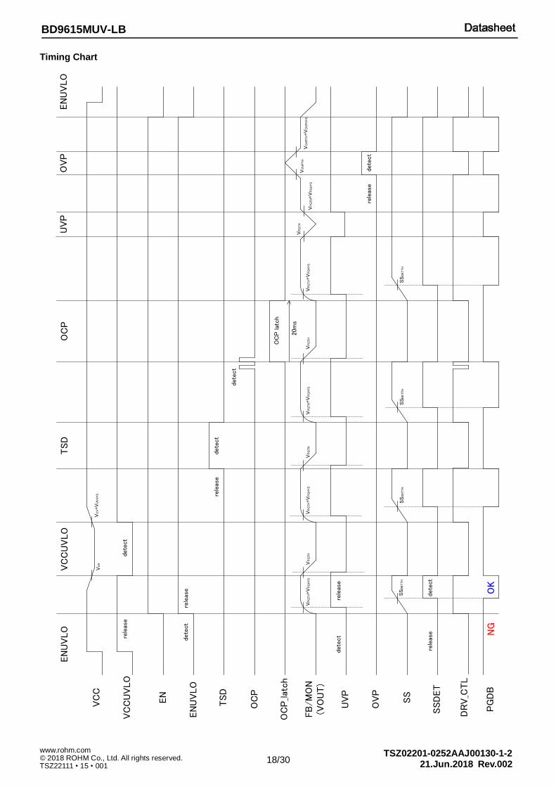
14. SSDET This is a Soft Start finish detect block. If the SS pin voltage is SSDETTH (1.2V (Typ)) or more, SSDET output is high. Output signal is added with other protection feature detection signals, and is output from the PGDB pin.
15. Power Good This block generates an output signal that is the output voltage state of Normal or Error.

5/30
BD9615MUV-LB
© 2018 ROHM Co., Ltd. All rights reserved. TSZ02201-0252AAJ00130-1-2
21.Jun.2018 Rev.002
www.rohm.com
TSZ22111 • 15 • 001
Absolute Maximum Ratings (Ta=25°C)
Parameter Symbol Rating Unit
Supply Voltage VCC to GND EN to GND PGDB to GND
VCC VEN
VPGDB 62 V
Supply Voltage VREG to GND OUT to GND
VREG 12 V
Supply Voltage VREF, SS, FB, COMP, MDT, RT, SYNC, OCP_P, OCP_M, MON to GND
VREF, VSS, VFB, VCOMP, VMDT, VRT, VSYNC, VOCP_P,
VOCP_M, VMON 7 V
Storage Temperature Range Tstg -55 to +150 °C
Maximum Junction Temperature Tjmax 150 °C
Caution 1: Operating the IC over the absolute maximum ratings may damage the IC. The damage can either be a short circuit between pins or an open circuit
between pins and the internal circuitry. Therefore, it is important to consider circuit protection measures, such as adding a fuse, in case the IC is operated over the absolute maximum ratings.
Caution 2: Should by any chance the maximum junction temperature rating be exceeded the rise in temperature of the chip may result in deterioration of the properties of the chip. Increase the board size and copper area to prevent exceeding the maximum junction temperature rating.
Thermal Resistance(Note 1)
Parameter Symbol Thermal Resistance (Typ)
Unit 1s(Note 3) 2s2p(Note 4)
VQFN16KV3030
Junction to Ambient θJA 189.0 57.5 °C/W
Junction to Top Characterization Parameter(Note 2) ΨJT 23 10 °C/W
(Note 1) Based on JESD51-2A(Still-Air). (Note 2) The thermal characterization parameter to report the difference between junction temperature and the temperature at the top center of the outside surface of the component package. (Note 3) Using a PCB board based on JESD51-3.
Layer Number of Measurement Board
Material Board Size
Single FR-4 114.3mm x 76.2mm x 1.57mmt
Top
Copper Pattern Thickness
Footprints and Traces 70μm
(Note 4) Using a PCB board based on JESD51-5, 7.
Layer Number of Measurement Board
Material Board Size Thermal Via(Note 5)
Pitch Diameter
4 Layers FR-4 114.3mm x 76.2mm x 1.6mmt 1.20mm Φ0.30mm
Top 2 Internal Layers Bottom
Copper Pattern Thickness Copper Pattern Thickness Copper Pattern Thickness
Footprints and Traces 70μm 74.2mm x 74.2mm 35μm 74.2mm x 74.2mm 70μm
(Note 5) This thermal via connects with the copper pattern of all layers.
Recommended Operating Conditions
Parameter Symbol Min Typ Max Unit
Power Supply Voltage VCC 3.5 12 60 V
Switching Frequency fOSC 100 500 2500 kHz
Switching Frequency Setting Resistor RRT 19 100 500 kΩ
External Synchronize Frequency fEXT 100 - 2500 kHz
External Synchronize Frequency for RT Setting Frequency
- -20 - +20 %
Operating Temperature Topr -40 +25 +105 °C
6/30
BD9615MUV-LB
© 2018 ROHM Co., Ltd. All rights reserved. TSZ02201-0252AAJ00130-1-2
21.Jun.2018 Rev.002
www.rohm.com
TSZ22111 • 15 • 001
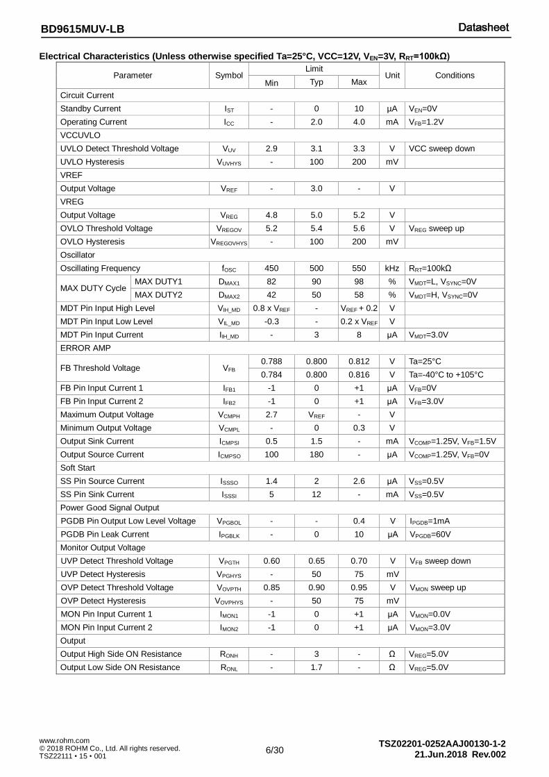
Electrical Characteristics (Unless otherwise specified Ta=25°C, VCC=12V, VEN=3V, RRT=100kΩ)
Parameter Symbol Limit
Unit Conditions Min Typ Max
Circuit Current
Standby Current IST - 0 10 µA VEN=0V
Operating Current ICC - 2.0 4.0 mA VFB=1.2V
VCCUVLO
UVLO Detect Threshold Voltage VUV 2.9 3.1 3.3 V VCC sweep down
UVLO Hysteresis VUVHYS - 100 200 mV
VREF
Output Voltage VREF - 3.0 - V
VREG
Output Voltage VREG 4.8 5.0 5.2 V
OVLO Threshold Voltage VREGOV 5.2 5.4 5.6 V VREG sweep up
OVLO Hysteresis VREGOVHYS - 100 200 mV
Oscillator
Oscillating Frequency fOSC 450 500 550 kHz RRT=100kΩ
MAX DUTY Cycle MAX DUTY1 DMAX1 82 90 98 % VMDT=L, VSYNC=0V
MAX DUTY2 DMAX2 42 50 58 % VMDT=H, VSYNC=0V
MDT Pin Input High Level VIH_MD 0.8 x VREF - VREF + 0.2 V
MDT Pin Input Low Level VIL_MD -0.3 - 0.2 x VREF V
MDT Pin Input Current IIH_MD - 3 8 μA VMDT=3.0V
ERROR AMP
FB Threshold Voltage VFB 0.788 0.800 0.812 V Ta=25°C
0.784 0.800 0.816 V Ta=-40°C to +105°C
FB Pin Input Current 1 IFB1 -1 0 +1 μA VFB=0V
FB Pin Input Current 2 IFB2 -1 0 +1 μA VFB=3.0V
Maximum Output Voltage VCMPH 2.7 VREF - V
Minimum Output Voltage VCMPL - 0 0.3 V
Output Sink Current ICMPSI 0.5 1.5 - mA VCOMP=1.25V, VFB=1.5V
Output Source Current ICMPSO 100 180 - μA VCOMP=1.25V, VFB=0V
Soft Start
SS Pin Source Current ISSSO 1.4 2 2.6 μA VSS=0.5V
SS Pin Sink Current ISSSI 5 12 - mA VSS=0.5V
Power Good Signal Output
PGDB Pin Output Low Level Voltage VPGBOL - - 0.4 V IPGDB=1mA
PGDB Pin Leak Current IPGBLK - 0 10 μA VPGDB=60V
Monitor Output Voltage
UVP Detect Threshold Voltage VPGTH 0.60 0.65 0.70 V VFB sweep down
UVP Detect Hysteresis VPGHYS - 50 75 mV
OVP Detect Threshold Voltage VOVPTH 0.85 0.90 0.95 V VMON sweep up
OVP Detect Hysteresis VOVPHYS - 50 75 mV
MON Pin Input Current 1 IMON1 -1 0 +1 μA VMON=0.0V
MON Pin Input Current 2 IMON2 -1 0 +1 μA VMON=3.0V
Output
Output High Side ON Resistance RONH - 3 - Ω VREG=5.0V
Output Low Side ON Resistance RONL - 1.7 - Ω VREG=5.0V

7/30
BD9615MUV-LB
© 2018 ROHM Co., Ltd. All rights reserved. TSZ02201-0252AAJ00130-1-2
21.Jun.2018 Rev.002
www.rohm.com
TSZ22111 • 15 • 001
Electrical Characteristics (Unless otherwise specified Ta=25°C, VCC=12V, VEN=3V, RRT=100kΩ) - continued
Parameter Symbol Limit
Unit Conditions Min Typ Max
OCP
Over Current Detect Threshold VOCPTH 80 100 120 mV
OCP_P Pin Input Bias Current IOCP_P - 20 100 μA VOCP_P=0.1V
OCP_M Pin Input Bias Current IOCP_M - 50 100 μA VOCP_M=GND
Over Current Detect Latch Stop Time tOCP 10 20 30 ms
CTL
EN Pin Internal REG ON-Threshold VENON 0.3 - 1.4 V
EN Pin UVLO Threshold VENUV 1.7 1.8 1.9 V IC Output ON condition
EN Pin Source Current IEN 9.0 10.0 11.0 μA VEN=3V
SYNC
SYNC Pin Threshold Voltage High VSYNCH 2.0 - 5.5 V
SYNC Pin Threshold Voltage Low VSYNCL -0.3 - +0.8 V
SYNC Pin Input Current ISYNC 6 12 24 µA VSYNC=3V

8/30
BD9615MUV-LB
© 2018 ROHM Co., Ltd. All rights reserved. TSZ02201-0252AAJ00130-1-2
21.Jun.2018 Rev.002
www.rohm.com
TSZ22111 • 15 • 001
0
500
1,000
1,500
2,000
2,500
3,000
0 100 200 300 400 500
Fre
qu
en
cy :
fO
SC[k
Hz]
RRT [kΩ]
Detailed Description
Frequency Setting Function It can determine frequency input to PWM by using the RT pin. It establishes constant current in the IC by connecting a timing resistor, RRT. Oscillation frequency can be set from 100kHz to 2500kHz and calculated as follows.
𝑓𝑂𝑆𝐶 =1
20×10−9+𝑅𝑅𝑇 (50×109)⁄ [Hz]
External CLK for SYNC Function This IC can operate synchronization function by inputting an external CLK signal to the SYNC pin. Input CLK signal is limited within ±20% of the frequency set by the RT pin. LOW level is 0.8V or less, and HIGH level is 2.0V or more. Required width of H section and L section is 100ns or more. After the 3rd input pulse at the SYNC pin, falling edge of internal sawtooth wave synchronizes with the falling edge of the SYNC pin. If external CLK stops, the device transitions to self-running mode after 1.5 times of oscillation period.
SYNC
SYNC_LATCH
IC INTERNAL WAVE
Figure 5. Frequency Synchronization Function Timing Chart
Figure 4. Frequency vs RRT

9/30
BD9615MUV-LB
© 2018 ROHM Co., Ltd. All rights reserved. TSZ02201-0252AAJ00130-1-2
21.Jun.2018 Rev.002
www.rohm.com
TSZ22111 • 15 • 001
VCC
EN
VCCUVLO
+
-
Detailed Description - continued
In the Case of Not Using the Synchronization Function Although the SYNC pin is internally pulled down by a resistor, it is recommended to connect the SYNC pin to GND if the synchronization function is not in use.
Figure 6. Circuit Diagram of SYNC Pin Not in Use
MDT Pin Function
It can change MAX DUTY by processing the MDT pin If the MDT pin is connected to the GND pin, MAX DUTY is prescribed in DMAX1 and is limited to 90% (Typ). If the MDT pin is connected to the VREF pin, MAX DUTY is prescribed in DMAX2 and is limited to 50% (Typ). To prevent malfunction caused by noise, connect the MDT pin to the GND pin or the VREF pin. When External Synchronize Frequency is input from SYNC (fEXT), MAX DUTY is determined by the frequency (fOSC) set by the RT pin and MAX DUTY set by the MDT pin and is prescribed in DMAX_SYNC by following formula.
𝐷𝑀𝐴𝑋_𝑆𝑌𝑁𝐶 = (1 −
1
𝑓𝑂𝑆𝐶×(1−𝐷𝑀𝐴𝑋)
1
𝑓𝐸𝑋𝑇
) × 100 [%]
Where: MDT=GND: DMAX = DMAX1: 90% (Typ) MDT=VREF: DMAX = DMAX2: 50% (Typ)
UVLO Control Function by External Resistors
The EN pin has built-in precise reset function. The EN pin connected with a resistor divider from VCC, as shown in Figure 7, can set low voltage malfunction prevention more than internal UVLO. When it is used, establish REN1 and REN2, as shown in Figure 7, for any VCC start-up voltage VSTART [V] and VCC shutdown voltage VSTOP [V].
𝑅𝐸𝑁1 =𝑉𝑆𝑇𝐴𝑅𝑇−𝑉𝑆𝑇𝑂𝑃
𝐼𝐸𝑁 [Ω]
𝑅𝐸𝑁2 =𝑉𝐸𝑁𝑈𝑉×𝑅𝐸𝑁1
𝑉𝑆𝑇𝐴𝑅𝑇−𝑉𝐸𝑁𝑈𝑉 [Ω]
Figure 7. Circuit Diagram of UVLO External Setting Method
SYNC
GND
IEN=10μA (Typ)
VENUV=1.8V (Typ)
REN1
REN2

10/30
BD9615MUV-LB
© 2018 ROHM Co., Ltd. All rights reserved. TSZ02201-0252AAJ00130-1-2
21.Jun.2018 Rev.002
www.rohm.com
TSZ22111 • 15 • 001
ERROR AMP
VOUT
RFB1
RFB2++
-
R2 C3
CSS
COMPFB
SSISSSO
VFB
COMP
SS
VOUT
EN ON
tCOMP
Ideal line
1.0V
1.5V
Swiching start
OUT
ΔVSSFB
Boost application
COMP
SS
VOUT
EN ON
tCOMP
Ideal line
1.0V
1.5V
Swiching start
OUT
ΔVSS
Flyback application
Detailed Description - continued
Soft Start Time
Soft Start Time tSS is determined by Soft Start Time Setting Capacitor CSS, SS Source Current ISSSO, and the FB pin Threshold Voltage VFB. Set CSS capacitance that can be fully discharged during the “Hiccup” time when OCP is detected.
𝑡𝑠𝑠 = 𝐶𝑆𝑆 ×𝑉𝐹𝐵
𝐼𝑆𝑆𝑆𝑂 [s]
In addition, when COMP terminal capacitor C3 is big and CSS is small, rise voltage ΔVSS of the SS pin voltage becomes big at time tCOMP before COMP pin voltage arriving at lower voltage of the internal saw-tooth wave (1.0V) from EN ON, and rush current occurs at the time of switching start. tCOMP, ΔVSS is calculated in the following formula. Set CSS and COUT in consideration of rush current to be proportional to ΔVSS and COUT.
Figure 8. Error amplifier circuit diagram
Figure 9. Output voltage starting diagram
Boost application
𝑡𝐶𝑂𝑀𝑃 = 𝐶3 (√(𝑅𝐹𝐵2 + 𝑅2)2 +2×𝐶𝑆𝑆×𝑅𝐹𝐵2
𝐶3×𝐼𝑆𝑆(
𝑅2×𝑉𝐶𝐶
𝑅𝐹𝐵1+𝑅𝐹𝐵2+ 1) − (𝑅𝐹𝐵2 + 𝑅2)) +
𝐶𝑆𝑆×𝑉𝐶𝐶×𝑅𝐹𝐵2
𝐼𝑆𝑆×(𝑅𝐹𝐵1+𝑅𝐹𝐵2) [s]
Flyback application
𝑡𝐶𝑂𝑀𝑃 = 𝐶3 (√(𝑅𝐹𝐵1//𝑅𝐹𝐵1 + 𝑅2)2 +2×𝐶𝑆𝑆×𝑅𝐹𝐵1//𝑅𝐹𝐵1
𝐶3×𝐼𝑆𝑆− (𝑅𝐹𝐵1//𝑅𝐹𝐵1 + 𝑅2)) [s]
∆𝑉𝑆𝑆 =𝐼𝑆𝑆
𝐶𝑆𝑆× 𝑡𝐶𝑂𝑀𝑃 [V]
11/30
BD9615MUV-LB
© 2018 ROHM Co., Ltd. All rights reserved. TSZ02201-0252AAJ00130-1-2
21.Jun.2018 Rev.002
www.rohm.com
TSZ22111 • 15 • 001
VOVPTH = 0.9V (Typ)
VOUT
OVPRMON1
RMON2
MON
Detailed Description - continued
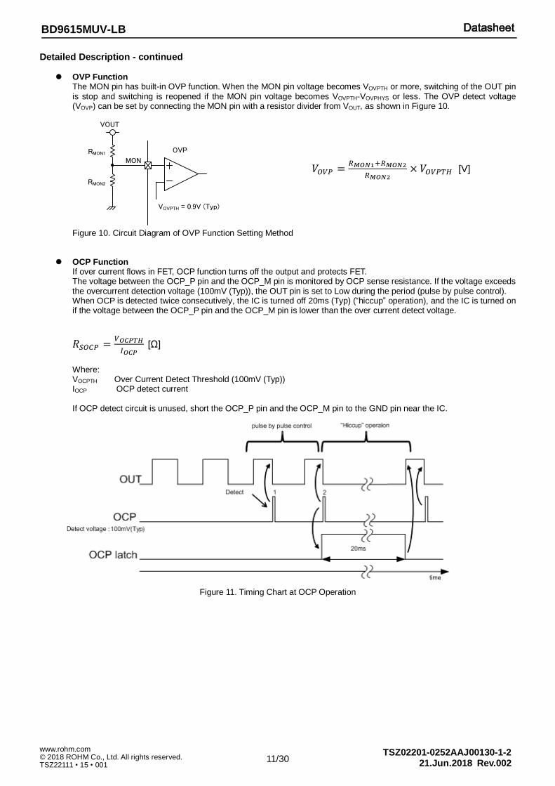
OVP Function
The MON pin has built-in OVP function. When the MON pin voltage becomes VOVPTH or more, switching of the OUT pin is stop and switching is reopened if the MON pin voltage becomes VOVPTH-VOVPHYS or less. The OVP detect voltage (VOVP) can be set by connecting the MON pin with a resistor divider from VOUT, as shown in Figure 10.
𝑉𝑂𝑉𝑃 =𝑅𝑀𝑂𝑁1+𝑅𝑀𝑂𝑁2
𝑅𝑀𝑂𝑁2× 𝑉𝑂𝑉𝑃𝑇𝐻 [V]
Figure 10. Circuit Diagram of OVP Function Setting Method
OCP Function If over current flows in FET, OCP function turns off the output and protects FET. The voltage between the OCP_P pin and the OCP_M pin is monitored by OCP sense resistance. If the voltage exceeds the overcurrent detection voltage (100mV (Typ)), the OUT pin is set to Low during the period (pulse by pulse control). When OCP is detected twice consecutively, the IC is turned off 20ms (Typ) (“hiccup” operation), and the IC is turned on if the voltage between the OCP_P pin and the OCP_M pin is lower than the over current detect voltage.
𝑅𝑆𝑂𝐶𝑃 =𝑉𝑂𝐶𝑃𝑇𝐻
𝐼𝑂𝐶𝑃 [Ω]
Where: VOCPTH Over Current Detect Threshold (100mV (Typ)) IOCP OCP detect current If OCP detect circuit is unused, short the OCP_P pin and the OCP_M pin to the GND pin near the IC.
Figure 11. Timing Chart at OCP Operation
12/30
BD9615MUV-LB
© 2018 ROHM Co., Ltd. All rights reserved. TSZ02201-0252AAJ00130-1-2
21.Jun.2018 Rev.002
www.rohm.com
TSZ22111 • 15 • 001
OCP_P Voltage
OCP_M
Voltage
OCP_P Voltage-OCP_M Voltage
OCPthOCP Detect
by Noise
OCP_P Voltage
OCP_M Voltage
OCP_P Voltage-OCP_M Voltage
OCPth
Before Measures After Measures
OCP_P
OCP_M
+
-
OCPOCP OCP Detect Resistance
Detailed Description – continued
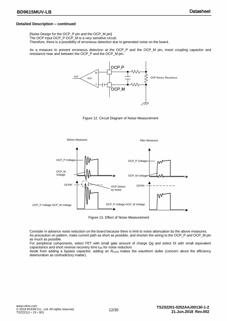
[Noise Design for the OCP_P pin and the OCP_M pin] The OCP input OCP_P OCP_M is a very sensitive circuit. Therefore, there is a possibility of erroneous detection due to generated noise on the board. As a measure to prevent erroneous detection at the OCP_P and the OCP_M pin, insert coupling capacitor and resistance near and between the OCP_P and the OCP_M pin.
Figure 12. Circuit Diagram of Noise Measurement
Figure 13. Effect of Noise Measurement
Consider in advance noise reduction on the board because there is limit to noise attenuation by the above measures. As precaution on pattern, make current path as short as possible, and shorten the wiring to the OCP_P and OCP_M pin as much as possible. For peripheral components, select FET with small gate amount of charge Qg and select Di with small equivalent capacitance and short reverse recovery time tRR for noise reduction. Aside from adding a bypass capacitor, adding an RGATE makes the waveform duller (concern about the efficiency deterioration as contradictory matter).

13/30
BD9615MUV-LB
© 2018 ROHM Co., Ltd. All rights reserved. TSZ02201-0252AAJ00130-1-2
21.Jun.2018 Rev.002
www.rohm.com
TSZ22111 • 15 • 001
VCC
OUT
PGDB
VOUT
VCC
VOUT
OUT
VREGBD9615MUV-LB
Detailed Description – continued
VREG Pin Function The VREG pin is output pin of internal regulator and it supplies 5.0V (Typ). It drives Nch MOSFET via the OUT pin of driver output. [Output Voltage Regenerative Function] For the power consumption improvement of the VREG, it can regenerate to the VREG pin via diode when voltage is upper than VREGOV. Voltage range that can regeneration is VREGOV (5.4V (Typ)) to 10V.
Figure 14. Example of Regeneration Application
[VCC Reduced Voltage] Due to decrease of VCC supply voltage, drive voltage output from the VREG pin also decrease and driver RON of the OUT pin is increased. Optimal drive voltage of FET is changed by oscillation frequency and the gate capacitance. Selects FET and oscillation frequency that consider characteristic data when use at VCC is less than or equal to 5V.
Power Good Output Function
The PGDB pin is the open drain output of the internal Nch FET. Using external resistance, pull up the PGDB pin to external power supply by external resister, to use Power Good Output function. When an internal detection function is the non-detection, and output voltage is within the range from UVP (the FB pin) to OVP (the MON pin), the PGDB pin is Low. When other operation mode or shutdown (EN=L), Nch MOSFET turns off and the PGDB pin turns HIGH (pull-up voltage). In addition, a connection between power supply (VCC) and output (VOUT) can be cut by connecting the PGDB pin like Figure 15. Pull-up voltage of the PGDB pin has to be below its absolute maximum rating of 62V.
Figure 15. Circuit Diagram of Power Line Cutting Method

14/30
BD9615MUV-LB
© 2018 ROHM Co., Ltd. All rights reserved. TSZ02201-0252AAJ00130-1-2
21.Jun.2018 Rev.002
www.rohm.com
TSZ22111 • 15 • 001
0.0
0.1
0.2
0.3
0.4
0.5
0.6
0.7
0.8
0.9
1.0
0 10 20 30 40 50 60
Sta
nd
by C
urr
en
t :
I ST
[µ
A]
Power Supply Voltage : VCC [V]
0.0
0.5
1.0
1.5
2.0
2.5
3.0
0 10 20 30 40 50 60
Op
era
tin
g C
urr
en
t :
I CC
[mA
]Power Supply Voltage : VCC [V]
3.0
3.1
3.2
3.3
3.4
3.5
-40 -20 0 20 40 60 80 100 120
UV
LO
Th
resh
old
[V
]
Temperature [˚C]
0.0
1.0
2.0
3.0
4.0
5.0
6.0
7.0
8.0
9.0
10.0
0 10 20 30 40 50 60
VR
EG
Ou
tpu
t V
olt
ag
e :
VR
EG
[V]
Power Supply Voltage : VCC [V]
Performance Curves (Reference Data) (Unless Otherwise Specified, Ta=25°C, VCC=12V)
Figure 16. Standby Current vs Power Supply Voltage Figure 17. Operating Current vs Power Supply Voltage
(VFB=1.2V)
release
detect
Figure 18. UVLO Threshold vs Temperature Figure 19. VREG Output Voltage vs Power Supply Voltage
15/30
BD9615MUV-LB
© 2018 ROHM Co., Ltd. All rights reserved. TSZ02201-0252AAJ00130-1-2
21.Jun.2018 Rev.002
www.rohm.com
TSZ22111 • 15 • 001
4.80
4.85
4.90
4.95
5.00
5.05
5.10
5.15
5.20
-40 -20 0 20 40 60 80 100 120
VR
EG
Ou
tpu
t V
olt
ag
e :
VR
EG
[V
]
Temperature [˚C]
0
10
20
30
40
50
60
70
80
90
100
-40 -20 0 20 40 60 80 100 120
MA
X D
UT
Y C
ycle
: D
MA
X [%
]
Temperature [˚C]
4.80
4.85
4.90
4.95
5.00
5.05
5.10
5.15
5.20
0 5 10 15 20
VR
EG
Ou
tpu
t V
olt
ag
e :
VR
EG
[V
]
VREG Output Current : IVREG [mA]
Performance Curves (Reference Data) - continued
450
460
470
480
490
500
510
520
530
540
550
-40 -20 0 20 40 60 80 100 120
Oscil
lati
ng
Fre
qu
en
cy :
fO
SC
[kH
z]
Temperature [˚C]
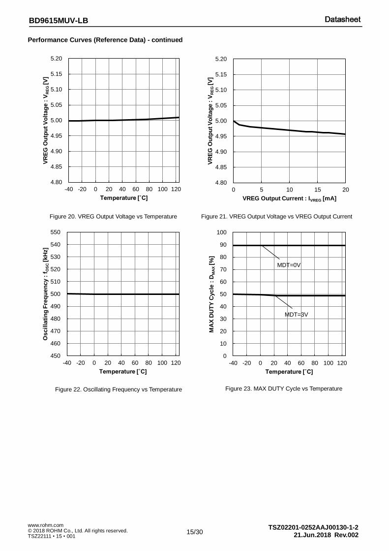
Figure 20. VREG Output Voltage vs Temperature Figure 21. VREG Output Voltage vs VREG Output Current
Figure 22. Oscillating Frequency vs Temperature Figure 23. MAX DUTY Cycle vs Temperature
MDT=0V
MDT=3V

16/30
BD9615MUV-LB
© 2018 ROHM Co., Ltd. All rights reserved. TSZ02201-0252AAJ00130-1-2
21.Jun.2018 Rev.002
www.rohm.com
TSZ22111 • 15 • 001
0.780
0.784
0.788
0.792
0.796
0.800
0.804
0.808
0.812
0.816
0.820
0 10 20 30 40 50 60
FB
Th
resh
old
Vo
ltag
e :
VF
B [V
]
Power Supply Voltage : VCC [V]
0.780
0.784
0.788
0.792
0.796
0.800
0.804
0.808
0.812
0.816
0.820
-40 -20 0 20 40 60 80 100 120
FB
Th
resh
old
Vo
ltag
e :
VF
B [V
]
Temperature [˚C]
0
1
2
3
4
5
6
7
8
-40 -20 0 20 40 60 80 100 120
Ou
tpu
t H
igh
Sid
e O
N R
esis
tan
ce :
RO
NH
[Ω]
Temperature [˚C]
0
1
2
3
4
5
6
7
8
-40 -20 0 20 40 60 80 100 120
Ou
tpu
t L
ow
Sid
e O
N R
esis
tan
ce :
RO
NL
[Ω]
Temperature [˚C]
Performance Curves (Reference Data) - continued
Figure 24. FB Threshold Voltage vs Power Supply Voltage
Figure 25. FB Threshold Voltage vs Temperature
VCC=3.5V
VCC=12V
VCC=12V
VCC=3.5V
Figure 26. Output High Side ON Resistance vs Temperature
Figure 27. Output Low Side ON Resistance vs Temperature

17/30
BD9615MUV-LB
© 2018 ROHM Co., Ltd. All rights reserved. TSZ02201-0252AAJ00130-1-2
21.Jun.2018 Rev.002
www.rohm.com
TSZ22111 • 15 • 001
9.0
9.2
9.4
9.6
9.8
10.0
10.2
10.4
10.6
10.8
11.0
-40 -20 0 20 40 60 80 100 120
EN
pin
So
urc
e C
urr
en
t :
I EN
[µ
A]
Temperature [˚C]
80
85
90
95
100
105
110
115
120
-40 -20 0 20 40 60 80 100 120
Over
Cu
rren
t D
ete
ct
Th
resh
old
: V
OC
PT
H[m
V]
Temperature [˚C]
Performance Curves (Reference Data) - continued
Figure 28. EN pin Source Current vs Temperature Figure 29. Over Current Detect Threshold vs Temperature
18/30
BD9615MUV-LB
© 2018 ROHM Co., Ltd. All rights reserved. TSZ02201-0252AAJ00130-1-2
21.Jun.2018 Rev.002
www.rohm.com
TSZ22111 • 15 • 001
EN
EN
UV
LO
TSD
OC
P_lat
ch
FB
/MO
N(V
OU
T)
UV
P
OV
P
SSD
ET
PG
DB
20m
s
OC
P lat
ch
OK
NG
VC
C
VC
CU
VLO
dete
ct
OC
P
SS
DR
V_C
TL
VC
CU
VLO
TSD
OC
PU
VP
OV
PEN
UV
LO
EN
UV
LO
VU
VV
UV+V
UV
HYS
VP
GTH+V
PG
HYS
VP
GTH
VP
GTH+V
PG
HYS
VP
GTH
VP
GTH+V
PG
HYS
VP
GTH
VP
GTH+V
PG
HYS
VP
GTH
VP
GTH+V
PG
HYS
VO
VP
TH+V
OV
PH
YS
VO
VP
TH
SS
DETTH
SS
DETTH
SS
DETTH
SS
DETTH
rele
ase
rele
ase
dete
ct
dete
ct
dete
ct
dete
ctre
leas
e
rele
ase
dete
ct
rele
ase
rele
ase
dete
ct
Timing Chart
19/30
BD9615MUV-LB
© 2018 ROHM Co., Ltd. All rights reserved. TSZ02201-0252AAJ00130-1-2
21.Jun.2018 Rev.002
www.rohm.com
TSZ22111 • 15 • 001
0
10
20
30
40
50
60
70
80
90
100
1 10 100 1000
Eff
icie
ncy [
%]
Output Current [mA]
BD9615MUV-LB
1
4
3
2
12
9
10
11
16 15 14 13
5 6 7 8
MDT
SYNC
RT
SS
VREG
OUT
GND
OCP_M
PG
DB
VR
EF
EN
VC
C
MO
N
CO
MP
FB
OC
P_P
100kΩ
0.01μF
100pF
10kΩ 3300pF
39mΩ
1μF/25V
1μ
F/1
0V
1μF/50V
VIN
RB050LAM-60TFTR(ROHM)
RTR030N05FRATL(ROHM)
160k
Ω30
kΩ
4.3k
Ω22
0pF
160k
Ω30
kΩ
10μF/50V VOUT
47μF/16V
SW
6.8μH
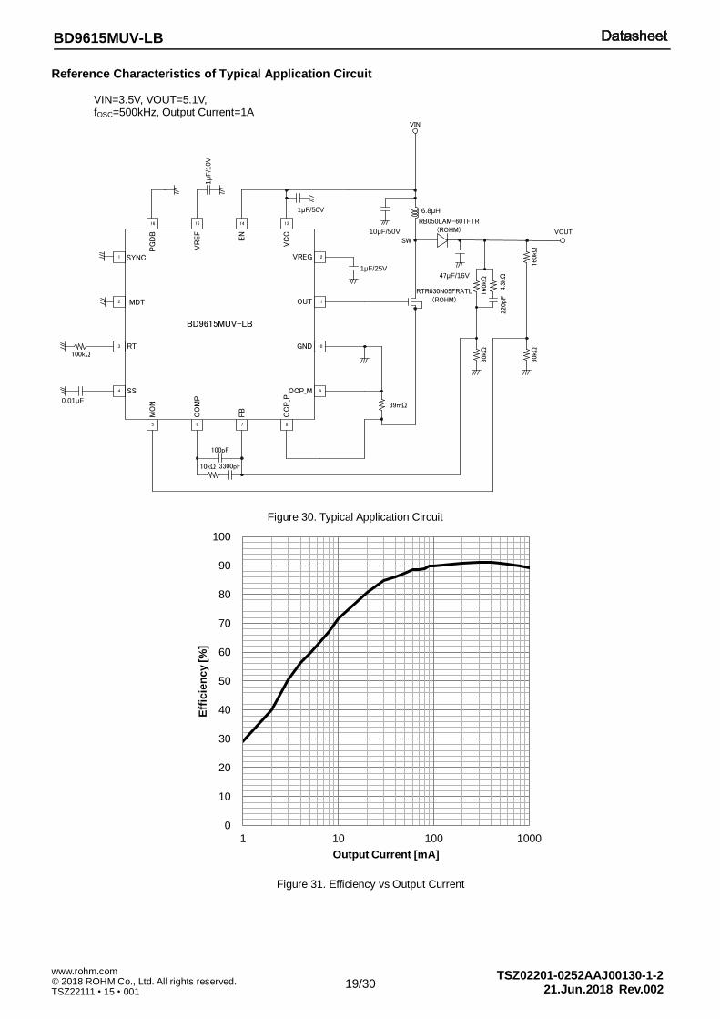
Reference Characteristics of Typical Application Circuit
VIN=3.5V, VOUT=5.1V, fOSC=500kHz, Output Current=1A
Figure 30. Typical Application Circuit
Figure 31. Efficiency vs Output Current

20/30
BD9615MUV-LB
© 2018 ROHM Co., Ltd. All rights reserved. TSZ02201-0252AAJ00130-1-2
21.Jun.2018 Rev.002
www.rohm.com
TSZ22111 • 15 • 001
Reference Characteristics of Typical Application Circuits - continued
Phase
Gain
Phase
Gain
Figure 32. Frequency Characteristics Output Current=0.1A
Figure 33. Frequency Characteristics Output Current=1.0A
EN 2.0V/div.
VOUT 5.0V/div.
SW 3.0V/div.
IL 1.0A/div.
EN 2.0V/div.
VOUT 5.0V/div.
SW 3.0V/div.
IL 1.0A/div.
Figure 34. Startup Waveform
Figure 35. Shutdown Waveform
2ms/div.
2ms/div.

21/30
BD9615MUV-LB
© 2018 ROHM Co., Ltd. All rights reserved. TSZ02201-0252AAJ00130-1-2
21.Jun.2018 Rev.002
www.rohm.com
TSZ22111 • 15 • 001
VFB
VOUT
RFB1
RFB2
FB
Application Part Setting Method
(1) Inductor It is recommended to use shielded type inductor that satisfies the current rating (IPEAK) and has low DCR (direct current resistance). Inductor value affects inductor ripple current and causes the output ripple. This ripple current can become small when inductor is large and switching frequency is high.
𝐼𝑃𝐸𝐴𝐾 = 𝐼𝑂𝑈𝑇𝑉𝑂𝑈𝑇
𝜂×𝑉𝐼𝑁+ 𝛥 𝐼𝐿 2⁄ [A] (1)
∆𝐼𝐿 =𝑉𝐼𝑁(𝑉𝑂𝑈𝑇−𝑉𝐼𝑁)
𝑉𝑂𝑈𝑇×𝑓𝑂𝑆𝐶×𝐿 [A] (2)
where: η is the efficiency ΔIL is the output ripple current fOSC is the switching frequency Normally, ΔIL is set 30% or less of Max Output Current (IOUTMAX).
When a current flowing into the inductor exceeds the inductor current rating, it causes a magnetic saturation which causes a decrease in efficiency and oscillation at the output. Choose an inductor with a sufficient margin so that peak current does not exceed current rating of the inductor.
(2) About Switching Components FET and Di
Set switching components with sufficient margin of current tolerance obtained by the formula (1). For noise and efficiency improvement, select FET with small input capacitance (CISS, Qg) and ON resistance. Select Di with small equivalent capacitance, short reverse recovery time tRR, and small forward voltage VF.
(3) Output Capacitor
Choose output capacitor with the lower Equivalent Series Resistance (ESR). Output Ripple Voltage VPP is determined in the formula (3).
𝑉𝑃𝑃 = 𝐼𝑂𝑈𝑇 ×𝑉𝑂𝑈𝑇−𝑉𝐼𝑁
𝐹𝑂𝑆𝐶×𝐶𝑂𝑈𝑇×𝑉𝑂𝑈𝑇+ 𝐼𝑃𝐸𝐴𝐾 × 𝐸𝑆𝑅 [V] (3)
Set within the range of allowable ripple voltage.
The VREF pin, the VREG pin connection capacitor
Between the VREF pin, the VREG pin and the GND pin is need to connect 1μF ceramic capacitor.
It is needed to select capacitor from 0.5μF to 1.5μF that considers DC bias effect and temperature characteristics.
In case capacitor short Grand fault is supposed, there is a possibility of destruction by generation of heat.
Therefore, it is needed to measure set the capacitor in two series.
(4) Input Capacitor
Input capacitor needs to use electrolytic capacitor and ceramic capacitor. Output switching current is supplied by Input Capacitor (CIN), so set ceramic bypass capacitor near FET and Di. When using electrolytic capacitor, consider the allowable ripple current.
(5) Output Voltage Setting
Output Voltage is determined in the formula (4)
𝑉𝑂𝑈𝑇 =𝑅𝐹𝐵1+𝑅𝐹𝐵2
𝑅𝐹𝐵2× 𝑉𝐹𝐵 [V] (4)
Figure 36. Inductor Current
Figure 37. Circuit Diagram of Voltage Feedback Resistor Setting Method
Δ IL∆IL

22/30
BD9615MUV-LB
© 2018 ROHM Co., Ltd. All rights reserved. TSZ02201-0252AAJ00130-1-2
21.Jun.2018 Rev.002
www.rohm.com
TSZ22111 • 15 • 001
A: ERROR Amp Gain=104 (=80dB) B: Oscillator amplitude=0.5V
Application Part Setting Method - continued
(6) Selection of External Phase Compensation Stable condition of application Negative feedback is applied is as follows. When Gain is 1(0dB), phase delay is 135 degrees or less (phase margin is 45 degrees or more). DC/DC converter application is sampled by switching frequency, so as a whole fBW (frequency at which gain is 0dB) is set 1/10 or less of the switching frequency. Also set fBW in less than 1/5 of boost converter peculiar right half plane zero (fRHPZ) so that right half plane zero frequency does not influence a control loop.
In conclusion, Application target specifications are as follows. (A) Gain is 1 (0dB), phase delay is 135 degrees or less (phase margin is 45 degrees or more).
(B) fBW is 1/10 or less of switching frequency
(C) fBW is 1/5 or less of fRHPZ
It set C1, C3, R1, and R2 of Figure 38 that meet the above. fBW that determines DC/DC converter responsiveness is able to calculate by evaluate 1st pole frequency and DC gain.
1st pole frequency 𝑓𝑝1 =1
(2𝜋×𝐴×𝑅𝐹𝐵1×𝑅𝐹𝐵2𝑅𝐹𝐵1+𝑅𝐹𝐵2
×𝐶3) [Hz]
DC Gain 𝐷𝐶𝑔𝑎𝑖𝑛 =𝐴
𝐵× 𝑉𝐹𝐵 ×
𝑉𝑂𝑈𝑇
𝑉𝐼𝑁
Where
𝑓𝐵𝑊 = 𝐷𝐶𝑔𝑎𝑖𝑛 × 𝑓𝑝1 [Hz]
𝑓𝑅𝐻𝑃𝑍 =1
2×𝜋×𝐿×𝐼𝑂𝑈𝑇×
𝑉𝐼𝑁2
𝑉𝑂𝑈𝑇 [Hz]
Insert second order phase lead in order to cancel the second order phase delay by LC. Insert phase lead near LC
resonance frequency.
Phase Lead 𝑓𝑧1 =1
2𝜋×𝑅𝐹𝐵1×𝐶1 [Hz]
Phase Lead 𝑓𝑧2 =1
2×𝜋×𝑅2×𝐶3 [Hz]
LC Resonance Frequency =1−𝐷
2×𝜋√𝐿×𝐶𝑂𝑈𝑇 [Hz]
Where COUT: Output Capacitor D: ON Duty=(VOUT-VIN)/VOUT
If fBW goes excessive high frequency by second order phase lead, it may be stabilized by inserting first order phase delay to frequency above LC resonance frequency to further compensate it.
Phase Delay 𝑓𝑝2 = 12×𝜋×𝑅1×𝐶1
[Hz]
Figure 38. Example of Phase Compensation Setting
COMP
VOUT
C3 RFB1
RFB2
R1
R2 C1

23/30
BD9615MUV-LB
© 2018 ROHM Co., Ltd. All rights reserved. TSZ02201-0252AAJ00130-1-2
21.Jun.2018 Rev.002
www.rohm.com
TSZ22111 • 15 • 001
PCB Layout Consider the following general points to bring out the IC performance.
1. Each input of the OCP_P pin and the OCP_M pin are very sensitive. Consider the above-mentioned contents. 2. For noise caused by parasitic capacitance coupling, consider routing by keep distance to providing a buffer zone.
Especially wiring those are sensitive to noise such as the OCP_P pin, the OCP_M pin and the COMP pin. 3. Near the OCP_P pin, the OCP_M pin and phase compensation circuit need to set pre-pattern about capacitor as
insurance. 4. Place the bypass capacitor near the input of the IC, FET, and Di and wire it as short as possible. 5. Be careful not to have common impedance to high current system with analog system VCC (GND).

24/30
BD9615MUV-LB
© 2018 ROHM Co., Ltd. All rights reserved. TSZ02201-0252AAJ00130-1-2
21.Jun.2018 Rev.002
www.rohm.com
TSZ22111 • 15 • 001
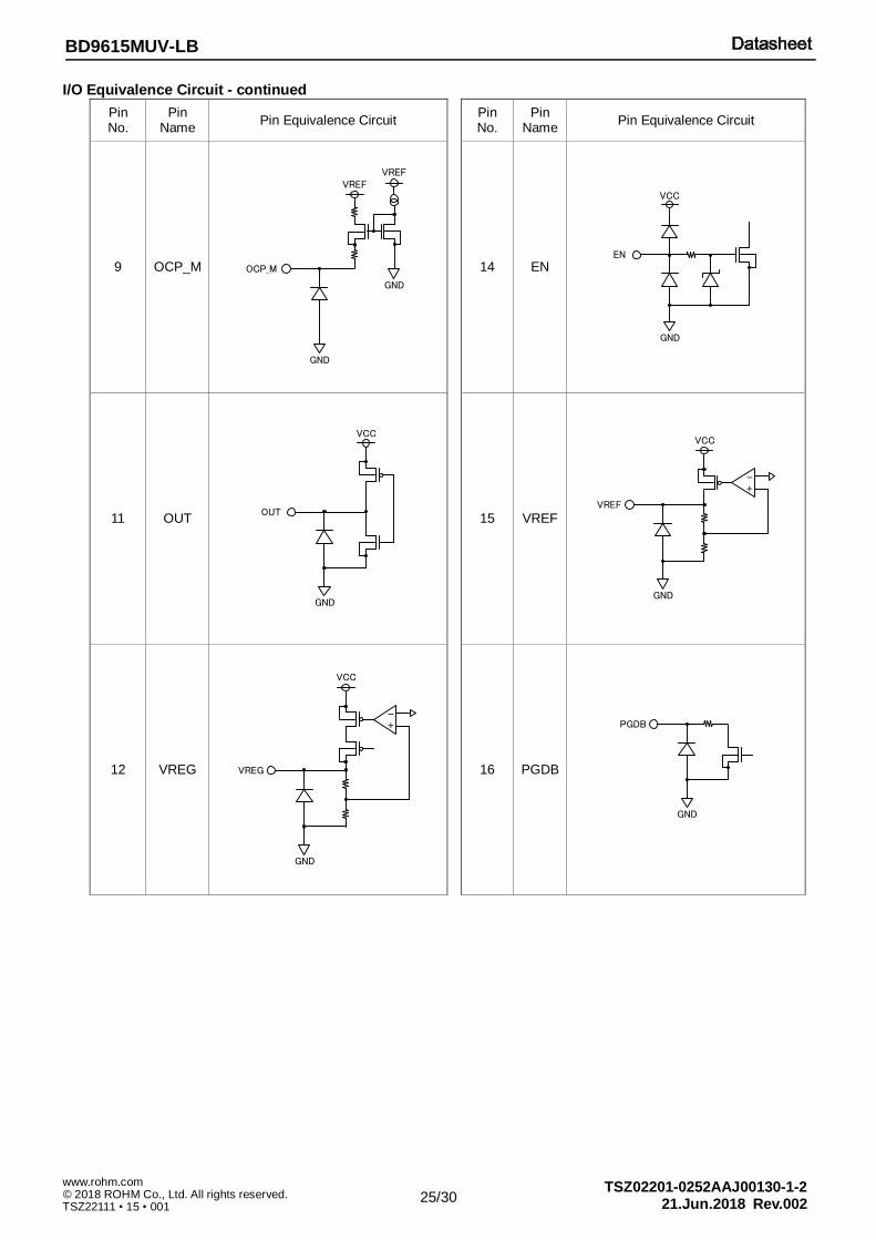
I/O Equivalence Circuit
Pin No.
Pin Name
Pin Equivalence Circuit Pin No.
Pin Name
Pin Equivalence Circuit
1 SYNC
5 MON
2 MDT
6 COMP
3 RT
7 FB
4 SS
8 OCP_P OCP_P
GND
VREF
GND
SYNC
GND
MON
GND
VREF
VREF
MDT
GND
COMP
GND
VREFVREF
-+
GND
RT
VREF
FB
GND
VREF
SS
GND
VREFVREF
25/30
BD9615MUV-LB
© 2018 ROHM Co., Ltd. All rights reserved. TSZ02201-0252AAJ00130-1-2
21.Jun.2018 Rev.002
www.rohm.com
TSZ22111 • 15 • 001
I/O Equivalence Circuit - continued
Pin No.
Pin Name
Pin Equivalence Circuit Pin No.
Pin Name
Pin Equivalence Circuit
9 OCP_M OCP_M
GND
VREFVREF
GND
14 EN
11 OUT
15 VREF
12 VREG
16 PGDB
VCC
EN
GND
OUT
GND
VCC
VREF
GND
+-
VCC
VREG
GND
+-
VCC
PGDB
GND

26/30
BD9615MUV-LB
© 2018 ROHM Co., Ltd. All rights reserved. TSZ02201-0252AAJ00130-1-2
21.Jun.2018 Rev.002
www.rohm.com
TSZ22111 • 15 • 001
Operational Notes
1. Reverse Connection of Power Supply Connecting the power supply in reverse polarity can damage the IC. Take precautions against reverse polarity when connecting the power supply, such as mounting an external diode between the power supply and the IC’s power supply pins.
2. Power Supply Lines Design the PCB layout pattern to provide low impedance supply lines. Furthermore, connect a capacitor to ground at all power supply pins. Consider the effect of temperature and aging on the capacitance value when using electrolytic capacitors.
3. Ground Voltage
Ensure that no pins are at a voltage below that of the ground pin at any time, even during transient condition.
4. Ground Wiring Pattern When using both small-signal and large-current ground traces, the two ground traces should be routed separately but connected to a single ground at the reference point of the application board to avoid fluctuations in the small-signal ground caused by large currents. Also ensure that the ground traces of external components do not cause variations on the ground voltage. The ground lines must be as short and thick as possible to reduce line impedance.
5. Recommended Operating Conditions
The function and operation of the IC are guaranteed within the range specified by the recommended operating conditions. The characteristic values are guaranteed only under the conditions of each item specified by the electrical characteristics.
6. Inrush Current When power is first supplied to the IC, it is possible that the internal logic may be unstable and inrush current may flow instantaneously due to the internal powering sequence and delays, especially if the IC has more than one power supply. Therefore, give special consideration to power coupling capacitance, power wiring, width of ground wiring, and routing of connections.
7. Operation Under Strong Electromagnetic Field
Operating the IC in the presence of a strong electromagnetic field may cause the IC to malfunction.
8. Testing on Application Boards When testing the IC on an application board, connecting a capacitor directly to a low-impedance output pin may subject the IC to stress. Always discharge capacitors completely after each process or step. The IC’s power supply should always be turned off completely before connecting or removing it from the test setup during the inspection process. To prevent damage from static discharge, ground the IC during assembly and use similar precautions during transport and storage.
9. Inter-pin Short and Mounting Errors Ensure that the direction and position are correct when mounting the IC on the PCB. Incorrect mounting may result in damaging the IC. Avoid nearby pins being shorted to each other especially to ground, power supply and output pin. Inter-pin shorts could be due to many reasons such as metal particles, water droplets (in very humid environment) and unintentional solder bridge deposited in between pins during assembly to name a few.
10. Unused Input Pins
Input pins of an IC are often connected to the gate of a MOS transistor. The gate has extremely high impedance and extremely low capacitance. If left unconnected, the electric field from the outside can easily charge it. The small charge acquired in this way is enough to produce a significant effect on the conduction through the transistor and cause unexpected operation of the IC. So unless otherwise specified, unused input pins should be connected to the power supply or ground line.

27/30
BD9615MUV-LB
© 2018 ROHM Co., Ltd. All rights reserved. TSZ02201-0252AAJ00130-1-2
21.Jun.2018 Rev.002
www.rohm.com
TSZ22111 • 15 • 001
Operational Notes – continued
11. Regarding the Input Pin of the IC This monolithic IC contains P+ isolation and P substrate layers between adjacent elements in order to keep them isolated. P-N junctions are formed at the intersection of the P layers with the N layers of other elements, creating a parasitic diode or transistor. For example (refer to figure below):
When GND > Pin A and GND > Pin B, the P-N junction operates as a parasitic diode. When GND > Pin B, the P-N junction operates as a parasitic transistor.
Parasitic diodes inevitably occur in the structure of the IC. The operation of parasitic diodes can result in mutual interference among circuits, operational faults, or physical damage. Therefore, conditions that cause these diodes to operate, such as applying a voltage lower than the GND voltage to an input pin (and thus to the P substrate) should be avoided.
Figure 39. Example of monolithic IC structure
12. Ceramic Capacitor When using a ceramic capacitor, determine a capacitance value considering the change of capacitance with temperature and the decrease in nominal capacitance due to DC bias and others.
13. Thermal Shutdown Circuit(TSD) This IC has a built-in thermal shutdown circuit that prevents heat damage to the IC. Normal operation should always be within the IC’s maximum junction temperature rating. If however the rating is exceeded for a continued period, the junction temperature (Tj) will rise which will activate the TSD circuit that will turn OFF power output pins. When the Tj falls below the TSD threshold, the circuits are automatically restored to normal operation. Note that the TSD circuit operates in a situation that exceeds the absolute maximum ratings and therefore, under no circumstances, should the TSD circuit be used in a set design or for any purpose other than protecting the IC from heat damage.
14. Over Current Protection Circuit (OCP) This IC incorporates an integrated overcurrent protection circuit that is activated when the load is shorted. This protection circuit is effective in preventing damage due to sudden and unexpected incidents. However, the IC should not be used in applications characterized by continuous operation or transitioning of the protection circuit.
N NP
+ P
N NP
+
P Substrate
GND
NP
+
N NP
+N P
P Substrate
GND GND
Parasitic
Elements
Pin A
Pin A
Pin B Pin B
B C
E
Parasitic
Elements
GNDParasitic
Elements
CB
E
Transistor (NPN)Resistor
N Region
close-by
Parasitic
Elements

28/30
BD9615MUV-LB
© 2018 ROHM Co., Ltd. All rights reserved. TSZ02201-0252AAJ00130-1-2
21.Jun.2018 Rev.002
www.rohm.com
TSZ22111 • 15 • 001
Ordering Information
B D 9 6 1 5 M U V - L B E 2
Part Number Package
MUV: VQFN16KV3030 Product Rank
LB: for Industrial applications Packaging specification E2: Embossed tape and reel
Marking Diagram
VQFN16KV3030 (TOP VIEW)
6 1 5
Part Number Marking
LOT Number
Pin 1 Mark
B D 9

DatasheetDatasheet
29/30
BD9615MUV-LB
© 2018 ROHM Co., Ltd. All rights reserved. TSZ02201-0252AAJ00130-1-2
21.Jun.2018 Rev.002
www.rohm.com
TSZ22111 • 15 • 001
Physical Dimension and Packing Information
Package Name VQFN16KV3030
<Tape and Reel information>
Embossed carrier tapeTape
Quantity
Direction of feed The direction is the 1pin of product is at the upper left when you hold
reel on the left hand and you pull out the tape on the right hand
3000pcs
E2
( )
30/30
BD9615MUV-LB
© 2018 ROHM Co., Ltd. All rights reserved. TSZ02201-0252AAJ00130-1-2
21.Jun.2018 Rev.002
www.rohm.com
TSZ22111 • 15 • 001
Revision History
Date Revision Changes
24.Apr.2018 001 New release
21.jun.2018 002 The Package Name was changed. VQFN16SV3030 → VQFN16KV3030

Notice-PAA-E Rev.003
© 2015 ROHM Co., Ltd. All rights reserved.
Notice
Precaution on using ROHM Products 1. If you intend to use our Products in devices requiring extremely high reliability (such as medical equipment
(Note 1),
aircraft/spacecraft, nuclear power controllers, etc.) and whose malfunction or failure may cause loss of human life, bodily injury or serious damage to property (“Specific Applications”), please consult with the ROHM sales representative in advance. Unless otherwise agreed in writing by ROHM in advance, ROHM shall not be in any way responsible or liable for any damages, expenses or losses incurred by you or third parties arising from the use of any ROHM’s Products for Specific Applications.
(Note1) Medical Equipment Classification of the Specific Applications
JAPAN USA EU CHINA
CLASSⅢ CLASSⅢ
CLASSⅡb CLASSⅢ
CLASSⅣ CLASSⅢ
2. ROHM designs and manufactures its Products subject to strict quality control system. However, semiconductor
products can fail or malfunction at a certain rate. Please be sure to implement, at your own responsibilities, adequate safety measures including but not limited to fail-safe design against the physical injury, damage to any property, which a failure or malfunction of our Products may cause. The following are examples of safety measures:
[a] Installation of protection circuits or other protective devices to improve system safety [b] Installation of redundant circuits to reduce the impact of single or multiple circuit failure
3. Our Products are not designed under any special or extraordinary environments or conditions, as exemplified below. Accordingly, ROHM shall not be in any way responsible or liable for any damages, expenses or losses arising from the use of any ROHM’s Products under any special or extraordinary environments or conditions. If you intend to use our Products under any special or extraordinary environments or conditions (as exemplified below), your independent verification and confirmation of product performance, reliability, etc, prior to use, must be necessary:
[a] Use of our Products in any types of liquid, including water, oils, chemicals, and organic solvents [b] Use of our Products outdoors or in places where the Products are exposed to direct sunlight or dust [c] Use of our Products in places where the Products are exposed to sea wind or corrosive gases, including Cl2,
H2S, NH3, SO2, and NO2
[d] Use of our Products in places where the Products are exposed to static electricity or electromagnetic waves [e] Use of our Products in proximity to heat-producing components, plastic cords, or other flammable items [f] Sealing or coating our Products with resin or other coating materials [g] Use of our Products without cleaning residue of flux (even if you use no-clean type fluxes, cleaning residue of
flux is recommended); or Washing our Products by using water or water-soluble cleaning agents for cleaning residue after soldering
[h] Use of the Products in places subject to dew condensation
4. The Products are not subject to radiation-proof design. 5. Please verify and confirm characteristics of the final or mounted products in using the Products. 6. In particular, if a transient load (a large amount of load applied in a short period of time, such as pulse. is applied,
confirmation of performance characteristics after on-board mounting is strongly recommended. Avoid applying power exceeding normal rated power; exceeding the power rating under steady-state loading condition may negatively affect product performance and reliability.
7. De-rate Power Dissipation depending on ambient temperature. When used in sealed area, confirm that it is the use in
the range that does not exceed the maximum junction temperature. 8. Confirm that operation temperature is within the specified range described in the product specification. 9. ROHM shall not be in any way responsible or liable for failure induced under deviant condition from what is defined in
this document.
Precaution for Mounting / Circuit board design 1. When a highly active halogenous (chlorine, bromine, etc.) flux is used, the residue of flux may negatively affect product
performance and reliability. 2. In principle, the reflow soldering method must be used on a surface-mount products, the flow soldering method must
be used on a through hole mount products. If the flow soldering method is preferred on a surface-mount products, please consult with the ROHM representative in advance.
For details, please refer to ROHM Mounting specification

Notice-PAA-E Rev.003
© 2015 ROHM Co., Ltd. All rights reserved.
Precautions Regarding Application Examples and External Circuits 1. If change is made to the constant of an external circuit, please allow a sufficient margin considering variations of the
characteristics of the Products and external components, including transient characteristics, as well as static characteristics.
2. You agree that application notes, reference designs, and associated data and information contained in this document
are presented only as guidance for Products use. Therefore, in case you use such information, you are solely responsible for it and you must exercise your own independent verification and judgment in the use of such information contained in this document. ROHM shall not be in any way responsible or liable for any damages, expenses or losses incurred by you or third parties arising from the use of such information.
Precaution for Electrostatic This Product is electrostatic sensitive product, which may be damaged due to electrostatic discharge. Please take proper caution in your manufacturing process and storage so that voltage exceeding the Products maximum rating will not be applied to Products. Please take special care under dry condition (e.g. Grounding of human body / equipment / solder iron, isolation from charged objects, setting of Ionizer, friction prevention and temperature / humidity control).
Precaution for Storage / Transportation 1. Product performance and soldered connections may deteriorate if the Products are stored in the places where:
[a] the Products are exposed to sea winds or corrosive gases, including Cl2, H2S, NH3, SO2, and NO2 [b] the temperature or humidity exceeds those recommended by ROHM [c] the Products are exposed to direct sunshine or condensation [d] the Products are exposed to high Electrostatic
2. Even under ROHM recommended storage condition, solderability of products out of recommended storage time period may be degraded. It is strongly recommended to confirm solderability before using Products of which storage time is exceeding the recommended storage time period.
3. Store / transport cartons in the correct direction, which is indicated on a carton with a symbol. Otherwise bent leads
may occur due to excessive stress applied when dropping of a carton. 4. Use Products within the specified time after opening a humidity barrier bag. Baking is required before using Products of
which storage time is exceeding the recommended storage time period.
Precaution for Product Label A two-dimensional barcode printed on ROHM Products label is for ROHM’s internal use only.
Precaution for Disposition When disposing Products please dispose them properly using an authorized industry waste company.
Precaution for Foreign Exchange and Foreign Trade act Since concerned goods might be fallen under listed items of export control prescribed by Foreign exchange and Foreign trade act, please consult with ROHM in case of export.
Precaution Regarding Intellectual Property Rights 1. All information and data including but not limited to application example contained in this document is for reference
only. ROHM does not warrant that foregoing information or data will not infringe any intellectual property rights or any other rights of any third party regarding such information or data.
2. ROHM shall not have any obligations where the claims, actions or demands arising from the combination of the Products with other articles such as components, circuits, systems or external equipment (including software).
3. No license, expressly or implied, is granted hereby under any intellectual property rights or other rights of ROHM or any third parties with respect to the Products or the information contained in this document. Provided, however, that ROHM will not assert its intellectual property rights or other rights against you or your customers to the extent necessary to manufacture or sell products containing the Products, subject to the terms and conditions herein.
Other Precaution 1. This document may not be reprinted or reproduced, in whole or in part, without prior written consent of ROHM.
2. The Products may not be disassembled, converted, modified, reproduced or otherwise changed without prior written consent of ROHM.
3. In no event shall you use in any way whatsoever the Products and the related technical information contained in the Products or this document for any military purposes, including but not limited to, the development of mass-destruction weapons.
4. The proper names of companies or products described in this document are trademarks or registered trademarks of ROHM, its affiliated companies or third parties.

DatasheetDatasheet
Notice – WE Rev.001© 2015 ROHM Co., Ltd. All rights reserved.
General Precaution 1. Before you use our Products, you are requested to carefully read this document and fully understand its contents.
ROHM shall not be in any way responsible or liable for failure, malfunction or accident arising from the use of any ROHM’s Products against warning, caution or note contained in this document.
2. All information contained in this document is current as of the issuing date and subject to change without any prior
notice. Before purchasing or using ROHM’s Products, please confirm the latest information with a ROHM sales representative.
3. The information contained in this document is provided on an “as is” basis and ROHM does not warrant that all
information contained in this document is accurate and/or error-free. ROHM shall not be in any way responsible or liable for any damages, expenses or losses incurred by you or third parties resulting from inaccuracy or errors of or concerning such information.