communicating via hdlc over a tdm interface with a quicc ...demonstration of hdlc mode via a tdm...
TRANSCRIPT

Freescale SemiconductorApplication Note
© Freescale Semiconductor, Inc., 2009. All rights reserved.
Freescale Semiconductor offers many devices with the QUICC Engine™ technology, a high-performance, multiprotocol processing block. A common use of the QUICC Engine block is to establish an HDLC communication path over a TDM interface, such as a T1 or E1 link. This application note describes the various sub-blocks used in the QUICC Engine communications engine for this application, discusses how the sub-blocks interoperate with each other, describes how to initialize them for the HDLC communication path, and provides a software demonstration of HDLC mode via a TDM interface using on-chip loopback.
The examples and demonstration software in this application note were developed and verified using the MPC8360E device in a MPC8360E-RDK system. This note applies to any MPC83xx or MPC85xx device with a QUICC Engine block, although small differences in device and system configuration will require minor changes to the software.
To locate any published errata or documentation updates issued after this note was released, please refer to the Freescale website listed on the back cover of this document.
Contents1. Introduction . . . . . . . . . . . . . . . . . . . . . . . . . . . . . . . . 22. QUICC Engine Sub-blocks Needed for a Single Channel
of HDLC over TDM . . . . . . . . . . . . . . . . . . . . . . . . . 53. QUICC Engine Control . . . . . . . . . . . . . . . . . . . . . . 74. QUICC Engine Baud Rate Generates and Clock
Routing . . . . . . . . . . . . . . . . . . . . . . . . . . . . . . . . . . . 75. Timeslot Assigner Description/Configuration . . . . 106. UCC Description/Configuration . . . . . . . . . . . . . . . 148. Conclusion . . . . . . . . . . . . . . . . . . . . . . . . . . . . . . . 179. Revision History . . . . . . . . . . . . . . . . . . . . . . . . . . . 17A. Code Listing . . . . . . . . . . . . . . . . . . . . . . . . . . . . . . 18
Communicating via HDLC over a TDM Interface with a QUICC Engine™ UCCby: Freescale Semiconductor, Inc
Document Number: AN4026Rev. 0, 12/2009

Communicating via HDLC over a TDM Interface with a QUICC Engine™ UCC, Rev. 0
2 Freescale Semiconductor
Introduction
1 IntroductionThe Freescale QUICC Engine block is a high-performance multiprotocol processing block available in many microprocessor devices. Because of the many different protocols and interfaces that the QUICC Engine block supports, it has a high degree of programmability. Depending on the protocol and interface required for an application, the number of sub-blocks used and the amount of initialization required can be significant. However, once initialized, the QUICC Engine block handles most of the protocol work, freeing the CPU to handle higher level tasks.
QUICC Engine communication channels are commonly used as an HDLC controller using a time slot on a TDM interface such as a T1 or E1 line. The following subsections provide the basic information required to configure a QUICC Engine block-enabled device for this application.
To demonstrate how an HDLC channel can be used over TDM on an MPC8360, a software demonstration example accompanies this applications note. As later sections introduce the sub-blocks of the QUICC Engine block, descriptions of how the example code configures and uses the sub-blocks are also provided. The software itself is both included in Appendix A of this document and available as a Freescale CodeWarrior project in an accompanying download.
1.1 Introduction to the MPC8360E Figure 1 provides a block diagram of the MPC8360E. The MPC8360E consists of three main functional blocks: an e300c1 Power Architecture™ core, a system interface unit (SIU), and the QUICC Engine block. The e300 core is the main CPU of the system and is responsible for running all user code. The demonstration code provided in this application note runs on the e300 core. The system interface unit provides the memory interfaces and system glue logic required to create a complete system on a chip.

Communicating via HDLC over a TDM Interface with a QUICC Engine™ UCC, Rev. 0
Freescale Semiconductor 3
Introduction
Although a detailed understanding of both the e300 core and system interface unit are required for use of the MPC8360, the focus of this applications note is on the QUICC Engine block.
Figure 1. MPC8360E Block Diagram
Note that other QUICC Engine block-based devices from Freescale have a similar architecture, with different CPU cores and/or speed options, different system interface options, and different QUICC Engine block performance and I/O options.
1.2 Review of TDM and HDLCA time division multiplexed (TDM) bus is commonly used in telecommunication systems. A T1 line is a type of TDM interface developed for digital transmission of voice between telephone switching offices in
Memory ControllersGPCM/UPM/SDRAM
32/64 DDR2 Interface Unit
PCI Bridge
Local Bus
Bus Arbitration
DUART
Dual I2C
4 Channel DMA
Interrupt Controller
Protection & Configuration
System Reset
Clock Synthesizer
System Interface Unit(SIU)
Local Bus
Baud RateGenerators
48 KB Multiuser RAM
Interrupt Controller
UC
C8
Timers
Accelerators
Dual 32-bit RISC CP
Serial DMA
2 GMII/RGMII/TBI/RTBI
8 MII/RMII/NMSI8 TDM Ports 2 UTOPIA/POS-PHY
(MPHY 124 Ports)
Parallel I/O
QUICC Engine™ Block
JTAG/COP
PowerManagement
Timers
FPU
Classic G2 MMUs
32 KBD-Cache
32 KBI-Cache
Security Enginee300c1 Core
PCI
DDRC1
UC
C7
UC
C6
UC
C5
UC
C4
UC
C3
UC
C2
UC
C1
MC
C
US
B
SP
I2
Time Slot Assigner
DDRC2
SP
I1
32 DDR2 Interface Unit
48 KB Instruction RAM
Parallel I/O

Communicating via HDLC over a TDM Interface with a QUICC Engine™ UCC, Rev. 0
4 Freescale Semiconductor
Introduction
North America; E1 lines are similar links used primarily outside of North America. The example code in this note is based on a T1 line.
Figure 2. Simple TDM Example
The physical interface to a T1 or E1 line is handled by a device called a framer, which handles data and clock recovery from the physical line. This device presents a TDM bus to the MPC8360E. This TDM bus consists of a fixed rate clock, two data lines (receive and transmit), and a fixed rate frame sync. With T1 and E1 lines, the frame sync is exactly 8 kHz. The period between frame syncs is called a frame. A T1 line is designed to carry 24 voice channels and one control channel. Each voice channel requires eight bits of data every frame. The control channel uses a single bit per frame, and is often call a framing bit. Thus, a T1 line has 193 bits of data per frame (eight bits per channel × 24 channels + one control bit). Each consecutive eight bits of the data line is considered one channel and is called a timeslot. The frame sync indicates the start of the frame.
The data clock of a T1 line is 1.544 Mhz (193 bits per frame × 8 kHz).
Unlike Ethernet, clocks and data are always running on a TDM bus. There is no hardware signaling to indicate when data is valid or not. This is desirable for a voice connection, as the digitized voice is flowing at a constant rate. However, if a TDM channel is to be used for a data connection, a higher level control mechanism must be used. The high level data link control, or HDLC, is a protocol commonly used on TDM buses for data transmission (see Figure 3).
HDLC is an OSI layer 2 protocol first designed to run over timeslots (or even sub-timeslots) of a TDM link. While it can be and is used without a TDM link, this note discusses how to use it with a TDM link. HDLC is designed for use with physical channels that continuously transmit data. It sends a specific idle pattern when no data is ready for transmission. When data is ready, it first sends a specific flag pattern to signal valid data. This is followed by an address byte, a control byte, the data bytes, a CRC, and a closing flag. This sequence allows receivers to detect when a line is no longer idle, determine whether the data is addressed to them, verify the data has not been damaged, and determine when the line has returned to an idle state. The QUICC Engine block’s UCC handles all HDLC processing.
Opening Flag Address Control Information (Optional) CRC Closing Flag
8 Bits 16 Bits 8 Bits 8n Bits 16 Bits 8 Bits
Figure 3. HDLC Framing Structure
TSA TDM
Slot
Slot
3
3 Slot
Slot
N
N
UCC2 UCC1
UCC2 UCC1
TDM Tx
TDM Rx
1 TDM Sync
1 TDM ClockQUICC Engine Block
Communicating via HDLC over a TDM Interface with a QUICC Engine™ UCC, Rev. 0
Freescale Semiconductor 5
QUICC Engine Sub-blocks Needed for a Single Channel of HDLC over TDM
In a T1 line, the control channel is sometimes managed directly by the framer device. When using such a device, the TDM interface in the MPC8360E should be programmed to skip the framing bit. If the application requires that the MPC8360E terminate the control channel, the TDM interface can be programmed to route the framing bit to the appropriate resource inside the QUICC Engine block.
1.3 Required DocumentationAt the time of this writing, the following documents were the most current MPC8360 documentation. Please consult these for further details. For your convenience, the document order numbers are included in parentheses. Please consult the Freescale website for updated documents or errata.
Note that the information about the QUICC Engine block in the separate QEIWRM manual supersedes the information in the MPC8360RM.
• MPC8360 PowerQUICC II Pro Integrated Communications Processor Family Reference Manual, revision 2 (MPC8360ERM)
• QUICC Engine™ Block Reference Manual with Protocol Interworking, revision 2 (QEIWRM)
• MPC8360E/MPC8358E PowerQUICC II Pro Processor Revision 2.x TBGA Silicon Hardware Specifications, revision 2 (MPC8360EEC)
2 QUICC Engine Sub-blocks Needed for a Single Channel of HDLC over TDM
Part of the complexity of using the QUICC Engine block stems from the many different sub-blocks involved in a particular application. However, this complexity is primarily limited to the initialization steps needed to setup a protocol. Once running, the QUICC Engine block handles much of the protocol processing leaving the CPU to handle higher-level tasks.
The QUICC Engine block bundles together a microcoded communications processing block with the necessary hardware to implement a variety of communication protocols. Within the QUICC Engine block, the sub-blocks relevant to this note are the communications processing block, baud rate generators, time slot assigner, and unified communication controllers (UCCs).
Note that this applications note is focused on terminating a single channel of HDLC traffic on a single UCC. If more channels are needed, multiple UCCs can be used. However, if the number of HDLC channels is large, the QUICC Engine has a multichannel controller (MCC) designed to handle up to 256 channels of HDLC traffic. Refer to the QEIWRM for more details on the MCC. The sections of this note describing the time slot assigner will be helpful to the MCC user.
The communications processing sub-block is the core of the QUICC Engine block. In the MPC8360E, it consists of two RISC communication processors (CP). Other QUICC Engine devices use different numbers of RISC cores to provide different levels of protocol processing performance. The RISC CPs run in real time using code from an on-chip ROM. e300 core software interacts with the CPs via shared memory that appears in the core’s memory map. The CP sub-block is documented in the “Configuration” chapter of the QEIWRM. The complete MPC8360 memory map is documented in the “Memory Map” chapter of the MPC8360RM.
Communicating via HDLC over a TDM Interface with a QUICC Engine™ UCC, Rev. 0
6 Freescale Semiconductor
QUICC Engine Sub-blocks Needed for a Single Channel of HDLC over TDM
The QUICC Engine block on the MPC8360E has eight UCCs. A UCC is a hardware block that is controlled by the RISC CPs to implement one of many available protocols. In this note, a UCC is configured to terminate a single HDLC channel. Each UCC has control structures in the shared memory. The e300 software must set up and manage some of these structures and registers in order to configure the UCC for the desired protocol. Each UCC has an independent hardware interface that can be internally connected to the time slot assigner or directly to external pins. UCCs are documented in a variety of chapters in the QEIWRM reference manual. The “Unified Communication Controllers (UCCs)” chapter provides common information for all UCC modes. The “UCC for Fast Protocols” chapter documents the common features when a UCC is used with a fast protocol (such as HDLC). Each protocol has its own chapter.
The time slot assigner (TSA) on the MPC8360E provides eight TDM interfaces. Each interface has independent set of pins. The hardware interface supports a broad range of TDM buses, including T1, E1, T3, E3, PCM highways, and ISDN buses as well as user-defined buses. The TSA includes programmable memory that is used to establish connections between timeslots on the TDM interfaces and the UCCs. The time slot assigner and clock multiplexing are documented in the “Serial Interface with Time-Slot Assigner” chapter of the QEIWRM.
The baud rate generators (BRG) are sub-blocks within the QUICC Engine block that are used to generate clocks for a variety of uses. Each BRG uses either an internal clock or one of several clock input pins as a reference clock. The BRGs have a highly programmable divider that can produce a wide range of output clocks from the input reference. The output of the BRGs can be used by many of the QUICC Engine blocks including the UCCs and TSA.
In this example, two BRGs are used to generate clocks that are similar in frequency to a T1 line’s clock and frame sync. In a real system, these clocks would be provided by the framer or other external hardware. The BRGs are used in this note to allow a self-contained example to be demonstrated. The BRGs are documented in the “QUICC Engine Multiplexing and Timers” chapter of the QEIWRM.
2.1 Summary of QUICC Engine Sub-Blocks and DocumentationThe following list provides a summary of the chapters in the MPC8360E Reference Manual, Rev 2 and the QEIWRM, Rev 2 that are relevant to this application note:
• MPC8360RM Chapter 2: Memory Map—provides a complete listing of internal resources and their associated locations in memory.
• QEIWRM Chapter 4: QUICC Engine Block Control—discusses how to initialize the communication processors in the QUICC Engine.
• QEIWRM Chapter 5: QUICC Engine Multiplexing and Timers—discusses the baud rate generators, selection of UCC connections (through the TDM bus or direct) and connects clocks to TDM interfaces.
• QEIWRM Chapter 6: Unified Communication Controllers (UCCs)—discusses common features of the UCCs for all modes and protocols.
• QEIWRM Chapter 7: UCC for Fast Protocols—discusses features of the UCC when used for fast protocols, such as HDLC.
• QEIWRM Chapter 14: HDLC Controller—discusses features of the UCC when used for HDLC.
Communicating via HDLC over a TDM Interface with a QUICC Engine™ UCC, Rev. 0
Freescale Semiconductor 7
QUICC Engine Control
• QEIWRM Chapter 21: Serial Interface with Time-Slot Assigner—discusses the operation of the TSA and TDM hardware interface options.
3 QUICC Engine ControlThe QUICC Engine RISC processors can be monitored and controlled by the e300 CPU. This is accomplished through the QUICC Engine command register (CECR). This register allows the CPU to issue commands to the RISC processors and monitor for completion of commands. Some of the common commands allow the CPU to initialize, start, or stop an individual UCC’s receivers and transmitters. A reset bit allows the CPU to reset the entire QUICC Engine block.
In the example code, the CECR is used after all QUICC Engine and UCC data structures are set up. Then, an “initialize RX & TX parameters” command is issued to the UCC. This command causes the QUICC Engine to set up all of its internal data structures based on the values set up by the user. After this command completes, the UCC is ready for work.
The CECR has many uses besides initialization as shown in this example. The available commands differ depending on the protocol used. Some common commands are “graceful stop transmit,” which is used when a transmitter is to shut down at the end of the current frame; “stop transmit,” which aborts transmission as soon as the FIFOs are empty; and “restart transmission,” which resumes data transmission at the point previously stopped. These commands allow individual UCCs to be stopped and started without affecting other UCCs or going through a complete re-initialization sequence.
Other commands provide support for handling error conditions and additional protocol controls. The “Configuration” chapter of the QEIWRM provides the full list of commands.
The QUICC Engine block contains a block of memory called the multiuser RAM, or MURAM. The MURAM is visible to both the QUICC Engine RISC processors and the e300 core. Each UCC has a block in the MURAM called the parameter RAM. This block is used for a variety of general and protocol specific settings. In certain modes (including HDLC), the UCC uses another block of MURAM for a virtual FIFO. Buffer descriptors, which are used to control receive and transmit data, can be located in MURAM or in main memory.
Each UCC has a set of registers within the QUICC Engine block’s memory map. These registers provide control of mode selections, interrupts, status, and more. These registers are not part of the MURAM space.
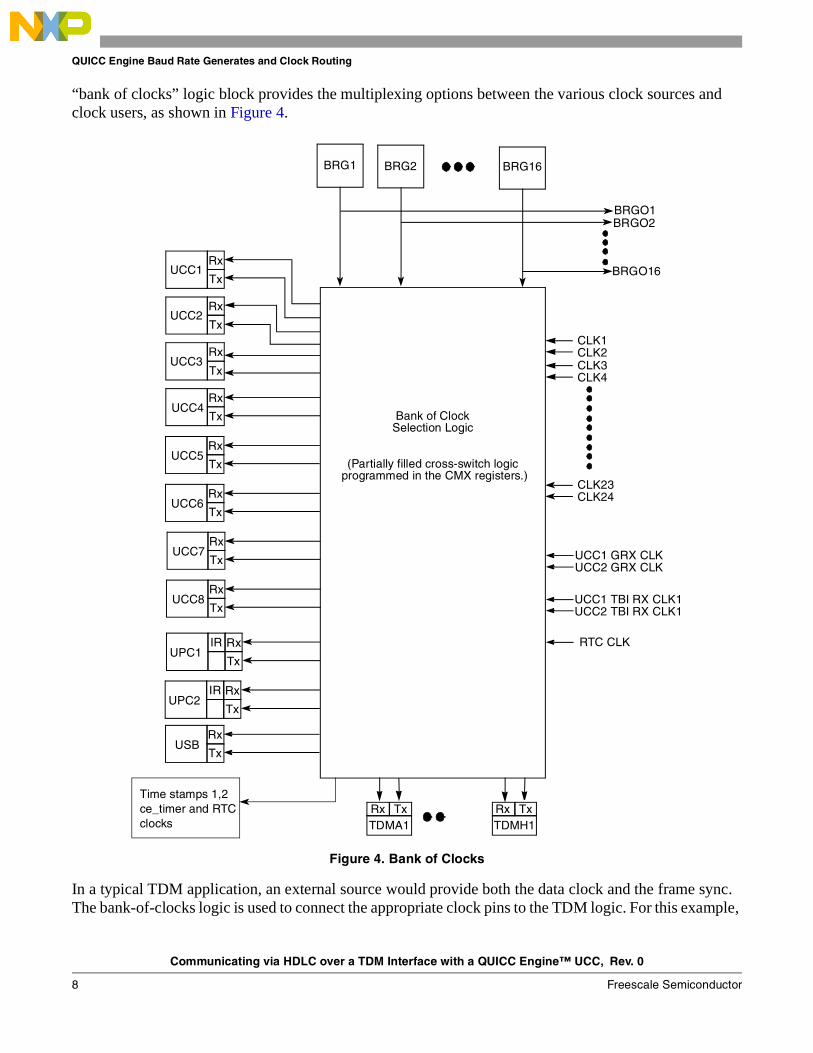
4 QUICC Engine Baud Rate Generates and Clock RoutingThe QUICC Engine block provides a great deal of flexibility in clock sources and clock users. Clocks used by the UCCs and TSA can be provided externally on a variety of clock pins or produced internally by the baud rate generators. In the MPC8360, there are 16 baud rate generators and 24 external clock inputs. A
Communicating via HDLC over a TDM Interface with a QUICC Engine™ UCC, Rev. 0
8 Freescale Semiconductor
QUICC Engine Baud Rate Generates and Clock Routing
“bank of clocks” logic block provides the multiplexing options between the various clock sources and clock users, as shown in Figure 4.
Figure 4. Bank of Clocks
In a typical TDM application, an external source would provide both the data clock and the frame sync. The bank-of-clocks logic is used to connect the appropriate clock pins to the TDM logic. For this example,
TDMA1TxRx
BRG1 BRG2 BRG16
BRGO1BRGO2
BRGO16
Bank of ClockSelection Logic
CLK1CLK2CLK3CLK4
CLK23CLK24
UCC1Tx
(Partially filled cross-switch logic programmed in the CMX registers.)
Rx
UCC2Tx
Rx
UCC3Tx
Rx
UCC4Tx
Rx
UCC5Tx
Rx
UCC6Tx
Rx
UCC7Tx
Rx
UCC8Tx
Rx
TDMH1TxRx
UPC1Tx
Rx
Time stamps 1,2ce_timer and RTCclocks
IR
UPC2Tx
RxIR
USBTx
Rx
UCC1 GRX CLKUCC2 GRX CLK
UCC1 TBI RX CLK1UCC2 TBI RX CLK1
RTC CLK

Communicating via HDLC over a TDM Interface with a QUICC Engine™ UCC, Rev. 0
Freescale Semiconductor 9
QUICC Engine Baud Rate Generates and Clock Routing
two baud rate generators are used to produce a data clock and a frame sync in order to avoid requiring an external clock source. The bank-of-clocks logic makes this easy by routing the two baud rate generators used to the TDM interface.
The baud rate generators work by dividing a source clock to a user programmable frequency. The source clock can be one of the external clock pins or the internal QUICC Engine clock. This choice of clock sources for the 16 BRGs provides significant flexibility in clock generation.
In this example, the QUICC Engine clock is used as the input for the two of the BRGs. This clock is referred to as the CE_CLK in MPC8360 Reference manual and the BRGCLK in the QEIWRM. CE_CLK/BRGCLK is generated by the QUICC Engine PLL, which is clocked by the PCI bus clock or CLKIN depending on system configuration. On the MPC8360-RDK, CE_CLK/BRGCLK is 250 MHz.
Figure 5 shows a baud-rate generator block diagram.
Figure 5. Baud-Rate Generator (BRG) Block Diagram
The baud rate generators consist of a pre-divider followed by a 12 bit divider. The predivider can divide the clock by one (i.e. no change) or 16. The divider’s range is from one to 4,096. (Note that programming the divider register to zero results in divide by one in the hardware.) Using both gives a division range of one to 65,536 (16 × 4,096).
In this example, the two BRGs are setup as follows:
• BRG3
— Divide by 16 turned off ( BRGC3[DIV6] bit = 0)
— Counter = 161 (BRGC[CD] = 0xA0).
— BRG3 output = 250 MHz ÷ (1 × 161) = 1.552 MHz.
• BRG11
— Divide by 16 turned on ( BRGC3[DIV6] bit = 1)
CLK Pin x ClockSourceMUX
Divide by1 or 16
Prescaler12-Bit Counter
1–4,096
DIV 16 CD[0–11]
BRGOn Clock
BRGCLK
EXTC
ATB
AutobaudControlRXDn
To Pin and/orBank of Clocks
BRGn
CLK Pin y
Communicating via HDLC over a TDM Interface with a QUICC Engine™ UCC, Rev. 0
10 Freescale Semiconductor
Timeslot Assigner Description/Configuration
— Counter = 1,953 (BRGC[CD] = 0x7A0).
— BRG11 output = 250 MHz ÷ (16 × 1,953) = 8.0005 kHz.
These clock frequencies are close to, but not exactly equal to, the rates used by a T1 line, which are 1.544 MHz for the data clock and 8.000 kHz for the frame sync. The ratio of data clock to frame sync is exactly 193 on a T1 line. In this example, the data clock is slightly faster with a ratio of 194.09. This allows for a close simulation of a T1 clock.
The QUICC Engine routing logic allows each UCC to be connected to its own set of independent pins or to an internal TDM bus. The independent mode is used for interfaces such as a UART or a Ethernet PHY port and is called non-multiplexed mode. The connection to the TDM internal bus is called multiplexed mode. The CMXUCRx registers documented in the “Multiplexing and Timers” chapter of the QEIWRM are used to make the selection between multiplexed and non-multiplexed mode. In this example, multiplexed mode is used.
A complete discussion of the UCC multiplexing, bank-of-clocks logic, and baud rate generators can be found in the “Multiplexing and Timers” chapter of the QEIWRM.
5 Timeslot Assigner Description/ConfigurationThe time slot assigner (TSA) is an interesting block that is often misunderstood. The source of this misunderstanding is the assumption that the TSA is an intelligent block with processing capability. It is not. The sole purpose of the TSA is to route clocks and data between the MPC8360’s eight TDM interfaces and the eight UCCs and two MCCs (multichannel controllers). It does this on a clock-by-clock basis based on the values programmed into the TSA’s RAM.
The TSA does have a large degree of flexibility and a number of options, which can seem like intelligence. However, the TSA is more accurately thought of as a simple state machine clocked by the TDM frame sync and TDM clock. State transitions occur at fixed times as programmed by the user in the TSA RAM. These fixed time periods define the time slots used by the system. Other options allow for selections of clock edges, delays between frame syncs and clocks, and more.
5.1 TSA RAMThe TSA RAM is the heart of the block. Each entry in the TSA RAM represents a time slice of the TDM bus. The entry itself defines how many clock periods it represents; this can vary from one to sixty-four. A frame sync causes the TSA to reset to the first entry in the RAM. The TSA steps through the entries in sequence until another frame sync occurs or an entry is programmed as “last.” There are no looping or repeat capabilities in the TSA.
Each entry in the TSA RAM contains a channel selection field. This field tells the TSA which UCC should be connected to the TDM bus during the time slice defined by the RAM entry. A “null” selection can also be used, which allows unused time slots to skipped.
The RAM entry can define from one to eight bits with single clock resolution, or one to eight bytes with 8-clock resolution. Consecutive RAM words can route the same UCC to allow for a wide variety of timeslot sizes. For example, a 15 bit timeslot could be created by a one byte RAM word followed by a seven bit RAM word.

Communicating via HDLC over a TDM Interface with a QUICC Engine™ UCC, Rev. 0
Freescale Semiconductor 11
Timeslot Assigner Description/Configuration
The TSA RAM has separate banks for receive and transmit. This allows different routing between receive and transmit. It also means that in system with identical receive and transmit routing, both banks must be programmed the same.
The TSA RAM can also be further divided into active and shadow banks, which allows dynamic changes to TSA RAM programming. When used, the TSA hardware switches the active and shadow banks on a frame sync for a seamless switchover. This mode is not used in this example.
The TSA block is responsible for the TDM hardware interfaces. As mentioned above, this includes edge and level selections and frame sync delays. Another important function supported by the TSA is diagnostic loopback. Loopback allows the TDM transmit pin to be connected to the receive pin. This is programmed in SDMx bits of the “SI MODE register” of the appropriate TDM interface. This mode is independent of the loopback mode in the UCC, and is the mode closest to the pins.
This example uses TDM loopback to demonstrate a communication path from a UCC transmitter, through the TDM transmit timeslot assignment, back through the TDM receive timeslot assignment, and then finally back to the UCC receiver.
The TSA RAM has a line size of 32 bits. TSA entries are 16 bits wide, thus the RAM holds two entries per line. In the QEIWRM, TSA memory maps are shown as 32-bits wide with two 16 bit entries per line. The reader is advised to pay attention to this nomenclature to avoid confusion.
A TSA RAM entry has the following fields, as shown in Figure 6:
The fields are as follows:
MCC: 1-bit that defines if an MCC is used. Set to 0 (no MCC) for this example.
SWTR: 1-bit to switch Tx and Rx lines for special hardware. Set to 0 (normal) for this example.
SSEL[1–4]: Four bits to control external strobes. Often used with custom hardware. All are 0 (no strobes) for this example.
SGS: 1 bit to select which strobe group (1–4 or 7–8) SSELx refer to. Set to 0. Not used for this example.
CSEL: 4 bits that select the UCC connected to this timeslot. Set to either 0000b (NULL) or 0100b (UCC8) in this example.
CNT[2–0]: 3 bits that specify the length of this timeslot in bits or bytes. Set to 1 byte in the example.
BYT: 1 bit that specifies if CNT is in bits or BYTEs. Set to 1 (BYTE) in this example.
LST: 1 bit that identifies the last entry in the RAM table. In this example, all but the last entry are set to 0. The last entry is set to 1.
Access: Read/Write
0 1 2 3 4 5 6 7 10 11 13 14 15
RMCC SWTR
SSEL1
SSEL2
SSEL3
SSEL4
SGS CSEL CNT BYT LSTW
Reset All zeros
Figure 6. SI RAM Entry for UCC
Communicating via HDLC over a TDM Interface with a QUICC Engine™ UCC, Rev. 0
12 Freescale Semiconductor
Timeslot Assigner Description/Configuration
The TSA entries for both Rx and Tx RAM are identical in this example. They are programmed to create 24 one-byte entries. This is similar to a T1 line. The entries used in this example are as shown in Table 1:
As no time slots after the second slot are used in this example, it could work with the second entry having its LST bit set. However, if another time slot were to be used, additional entries would need to be added. This, too, could be done differently, by modifying the CNT field in the first entry to skip unused timeslots. However, this example allows easy changes on a timeslot-by-timeslot basis without having to change the overall TSA RAM setup. If an application requires the ability of allowing configurable timeslot programming, the above approach simplifies software management of the TSA RAM.
Table 1. Example Entries
Entry Number CSEL CNT BYT LST
0 0 1 1 0
1 0100b (UCC8) 1 1 0
2 0 1 1 0
3 0 1 1 0
4 0 1 1 0
5 0 1 1 0
6 0 1 1 0
7 0 1 1 0
8 0 1 1 0
9 0 1 1 0
10 0 1 1 0
11 0 1 1 0
12 0 1 1 0
13 0 1 1 0
14 0 1 1 0
15 0 1 1 0
16 0 1 1 0
17 0 1 1 0
18 0 1 1 0
19 0 1 1 0
20 0 1 1 0
21 0 1 1 0
22 0 1 1 0
23 0 1 1 1

Communicating via HDLC over a TDM Interface with a QUICC Engine™ UCC, Rev. 0
Freescale Semiconductor 13
Timeslot Assigner Description/Configuration
5.2 TSA Mode Register SettingsThe TSA has several registers that must be understood and programmed for proper operation. Of particular importance is the mode register. Each of the eight TDM interfaces has an independent mode register, as shown in Figure 7.
The SIxMR registers are used to assign a portion of the TSA RAM to each TDM interface, control diagnostic modes, set clock edges and levels and frame sync delays. This example uses the TDM C interface. The settings used for SICMR are as follows:
SAD 0 = Use entries 0–31 of the TSA RAM. If other TDM interfaces are used, this must be different than the other interfaces.
SDM 11b = Loopback enabled. TDMC’s Tx signal is internally connected to its Rx signal. The external Tx pin is inactive. This is used to provide a stand alone example. In a real application, these bits would be set to 00b.
RFSD 00b = No delay from frame sync to first Rx bit. Some external hardware may require a delay between frame sync and the first bit of the frame, this field allows for delays of up to three clocks.
CRT 1 = common sync and clock for Rx and Tx. If an application has separate clocks and frame syncs for receive and transmit, this bit must be cleared.
SL 0 = active high sync. This bit selects the signal level for the frame sync. Set to match external hardware.
CE 1 = Tx on failing edge, Rx on rising edge. This bit selects the clock edges used to transmit and receive. Most external hardware requires this setting. If an IDL link is used, a setting of zero should be used.
FE 1 = frame sync on rising edge. This bit selects the clock edges used for the frame sync. Most external hardware requires this setting. If an IDL link is used, a setting of zero should be used.
GM 0 = no grant mode used. This bit is set for IDL mode. Grant mode is not used in most TDM applications.
TFSD 00b = No delay from frame sync to first Tx bit. Some external hardware may require a delay between frame sync and the first bit of the frame, this field allows for delays of up to three clocks.
Access: Read/Write
0 3 4 5 6 7 8 9 10 11 12 13 14 15
RSAD SDM RFSD — CRT SL CE FE GM TFSD
W
Reset All zeros
Figure 7. SI Mode Register (SIxMR)

Communicating via HDLC over a TDM Interface with a QUICC Engine™ UCC, Rev. 0
14 Freescale Semiconductor
UCC Description/Configuration
6 UCC Description/ConfigurationWith the TSA and its clock sources setup, the last step is to configure the UCC for HDLC mode. UCCs have many registers and data structures that must be configured. Because of the flexibility of the UCCs, these settings are documented across many chapters in the reference manual. The appropriate chapters depend on the protocol used.
UCCs require several data structures for operation. They are as follows:
• UCC registers located within the QUICC Engine memory map.
• UCC Parameter RAM located within MURAM.
• Virtual FIFOs (fast mode only) located within MURAM
• Rx and Tx buffer descriptors located within MURAM or main memory.
• Rx and Tx buffers located in main memory.
6.1 Common UCC SettingsThe “Unified Communications Controllers (UCCs)” chapter in the QEIWRM is common to all protocols. It provides an overview of UCC operation, documents registers common to all modes, provides memory offsets for each UCC’s memory block, and describes interrupt operation. This chapter is required reading for any use of the UCC.
Of particular note in this chapter is the “General UCC extended mode register,” section or GUEMR. UCC protocols are divided into two groups: fast and slow. A UART is a slow protocol while Ethernet and HDLC are fast protocols. The overview section of this chapter provides the complete list of slow and fast protocols. Each UCC’s GUEMR is used to select between fast and slow protocols. Furthermore, this selection is made separately for Rx and Tx directions, although in most cases the same protocol is run on both directions.
In this example, GUEMR of UCC8 has both the URMODE and UTMODE bits set, which selects a fast protocol. Note that this does not select the actual protocol.
6.2 Fast Mode UCC SettingsOnce the selection of a fast mode protocol is made, the “UCC for Fast Protocols” chapter should be reviewed. This chapter documents UCC registers when a fast protocol is used. While all registers should be reviewed, this note will discuss one register in particular and the virtual FIFOs.
In fast mode, UCCs implement virtual FIFOs in MURAM. The user must select an available block of MURAM for the FIFOs and set various size and threshold parameters. This example shows how the VFIFOs should be set for HDLC. For other protocols, section 7.5 of the “UCC for Fast Protocols” chapter in the QEIWRM provides the proper settings.

Communicating via HDLC over a TDM Interface with a QUICC Engine™ UCC, Rev. 0
Freescale Semiconductor 15
UCC Description/Configuration
The General UCC mode register (GUMR, not to be confused with GUEMR), shown in Figure 8, provides detailed control over the UCC’s hardware interface. This interface is either the external pins (non-multiplexed mode) or the TSA (multiplexed mode). In this example, the internal TDM bus is used.
Fast mode GUMR (documented in section 27.4.2.1) is set in this example as follows:
DIAG 00b = Normal mode. UCC loopback could be used here for diagnostic purposes.
TCI: 0 = normal. This bit must be cleared when the TSA is used.
TRX 0 = normal. When set, the receiver runs in transparent mode while the transmitter runs in the programmed protocol. This bit is set for unique applications or testing.
TTX 0 = normal. When set, the transmitter runs in transparent mode while the receiver runs in the programmed protocol. This bit is set for unique applications or testing.
CDP 0 = normal. This bit must be cleared when the UCC is used with the TSA and HDLC.
CTSP 1 = pulse mode. This bit must be set when the TSA is used.
CDS 1 = CD synchronous with data. This bit must be set when the TSA is used.
CTSS 1 = CTS synchronous with data. This bit must be set when the TSA is used.
TXSY: 0 = no synchronization between Rx and Tx.
RSYN 0 = normal mode. This field applies only in totally transparent mode.
SYNL 00b = external sync. This field applies only in totally transparent mode.
RTSM 1 = send flags/syncs between frames.
RENC 00b = Receiver uses NRZ decoding. Typical setting for HDLC.
REVD 0 = normal. This field applies only in totally transparent mode.
TENC 00b = Transmitter decoding. Typical setting for HDLC.
TCRC 00b = 16 bit CRC. This field applies only in totally transparent mode.
ENR 0 = Rx disabled/1 = Rx enabled. During initialization, this bit is cleared. It is set when initialization is complete.
ENT 0 = Tx disabled/1 = Tx enabled. During initialization, this bit is cleared. It is set when initialization is complete.
Access: Read/Write
0 1 2 3 4 5 6 7 8 9 13 14 15
RDIAG TCI TRX TTX CDP CTSP CDS CTSS — TXSY RSYN
W
Reset All zeros
16 17 18 19 20 21 22 23 24 25 26 27 28 31
RSYNL RTSM RENC REVD TENC TCRC ENR ENT MODE
W
Reset All zeros
Figure 8. General UCC Mode Register (Fast Protocols)

Communicating via HDLC over a TDM Interface with a QUICC Engine™ UCC, Rev. 0
16 Freescale Semiconductor
Description of Example Code
MODE 0000b = HDLC. HDLC mode is selected for this UCC.
There are many other UCC registers and parameter RAM entries that must be set up for proper operation. The example code provides details on how they are set.
6.3 UCC Buffers and Buffer DescriptorsAll UCCs, regardless of protocol, use buffer descriptors (BDs) to manage data buffers. An overview of buffer descriptors is provided in chapter 24, “UCC as Slow Communications Controllers.” Although HDLC is a fast protocol, the overview in this chapter is helpful for understanding how BDs work. The key difference for a fast protocol is that BDs do not have to reside in MURAM. Section 14.2.2 of the “HDLC Controller” chapter in the QEIWRM provides the details about buffer descriptors as used by an UCC in HDLC mode.
UCCs operate with a chain of receive and transmit BDs. A chain can be as small as one entry. For HDLC, the maximum size is limited only by available memory. Each BD contains a pointer to the buffer used to hold transmit or receive data. A status bit in the BD determines whether the UCC can use the BD to read or write data or if the e300 core controls the data. When reception or transmission is complete, the UCC changes this bit to indicate e300 core control.
The last entry in the chain of BDs is indicated by a “last” bit in the status field. This tells the UCC to return to the first BD in the chain. A field in the parameter RAM specifies the starting address of the buffer descriptor chain.
A transmit BD has a status bit that indicates the associated buffer should be transmitted continuously. In this case, the UCC does not clear the “ready” status bit in the BD after transmission is complete. Instead, it restarts transmission using the same BD. This causes the data in the associated buffer to be continuously transmitted. If the UCC is set up to create a frame on every buffer, each transmission will appear as one frame. This example utilizes this setup to create a continuous stream of transmit frames.
To simplify this example, a single receive BD and receive buffer are used. A single transmit BD and single transmit buffer are used as well. Both BDs are allocated in MURAM, while the buffers reside in main memory.
7 Description of Example CodeThe accompanying software example shows how to configure an MCP8360 for HDLC communication over a TDM link. The demonstration uses the TSA’s diagnostic loopback feature to operate without any external hardware. The software provides the details needed for initialization and operation of an HDLC channel on the MPC8360.
This demonstration does not implement functions that would most likely be used in real application. In particular, the following functions would need to be added:
• Interrupt generation and handling
• Multiple buffer descriptors
• Data buffer management
• Error management and recovery

Communicating via HDLC over a TDM Interface with a QUICC Engine™ UCC, Rev. 0
Freescale Semiconductor 17
Conclusion
The demonstration runs on the MPC8360E-RDK, which is a development board available from Freescale. The only connections needed to the board are a JTAG debugger (the Freescale USBTAP was used for this example), an RS-232 serial port, and power. The MPC8360E-RDK has two serial ports; this example uses the upper port. If connecting to a PC, a null-modem cable must be used. The serial port is configured to run at 57600 bps, eight bits, no parity, one stop bit (57600-8N1).
When run, the software sets up UCC8 to continuously transmit an HDLC frame with a text message through a timeslot on TDMC. It then monitors UCC8 for receive data and displays this data on the serial port. If left to run with no breakpoints, the text message will repeat forever on the serial port. Using a debugger, a breakpoint set at the printf function call allows the user to observe each receive event.
The software is built using Freescale’s CodeWarrior for Power Architecture, version 8.8. CodeWarrior includes a template for use on the MPC8360E-RDK. The template is accessed by creating a new project in CodeWarrior and using the “New Project Wizard.” The template includes the debugger scripts that initialize the system memory and simple startup software. The code used in this example replaces the “main.c” file used in the template created by the new project wizard.
8 ConclusionThe MPC8360 and other QUICC Engine block-based devices from Freescale offer a wide variety of protocol processing and connectivity options. The QUICC Engine block includes many different functional sub-blocks to provide this flexibility. Understanding how these sub-blocks interact and how to use each of these sub-blocks to meet applications’ requirements will speed development. Although this note focused on the use of the MPC8360 for the specific task of HDLC over a TDM line, the concepts covered here are applicable to many other applications and protocols.
9 Revision HistoryTable 2 provides a revision history for this application note.
Table 2. Document Revision History
Rev.Number
Date Substantive Change(s)
0 12/2009 Initial Public Release
Communicating via HDLC over a TDM Interface with a QUICC Engine™ UCC, Rev. 0
18 Freescale Semiconductor
Code Listing
Appendix A Code Listing/****************************************************************************/
// Applications Note AN4026 Example Code
//
// This file contains an example of how to setup an UCC in the MPC8360 to
// operate in HDLC mode using the Time Slot Assigner (TSA). This
// code has been written to run on the MPC8360E-RDK board. This code was
// developed starting with the MPC8360E-RDK project wizard available in
// CodeWarrior for Power Architecture. This code assumes the board has
// been configured using the initialization file associated with the default
// CodeWarrior project.
//
// This demo programs the UCC for HDLC mode through the TSA, and sets up the
// TSA to operate similar to a T1 line. The TSA is configured in loopback
// mode. The code then shows how a transmit buffer is setup and sent. As
// the TSA is in loopback, the receive process is demonstrated as well.
//
// To avoid dependence on an external clock for the simulated T1 interface,
// the MPC8360's baud rate generators are used to produce a pseudo frame
// sync and a clock. On the MPC8360-RDK, the QUICC Engine (QE) is clocked
// at 250 MHz. One baud rate generator (BRG) is set to divide by 161,
// yielding a 1.552 MHz clock which is used as the data clock. Another BRG
// uses a divider of 31,248 resulting in a 8.0005 kHz clock for use as a frame
// sync. Even though these clocks are not exactly T1 rates, they are close
// enough that they demonstrate the behavior of the system. If available,
// external clocks could be used.
//
// Note that references to specific sections of the "QUICC Engine Block
// Reference Manual with Protocol Interworking" (QEIWRM) revision 2, are
// included in the comments. They appear as "RM section X.Y.Z".
//
/****************************************************************************/
#include <stdio.h>
Communicating via HDLC over a TDM Interface with a QUICC Engine™ UCC, Rev. 0
Freescale Semiconductor 19
Code Listing
#include <string.h>
// The following defines establish the memory location of several key
// blocks inside the MPC8360.
// The IMMR setting is the base address of all internal chip memory.
// IMMR is set by hardware at reset, and can be changed by software.
// This define must be set to the same value as the hardware or initialization
// sets. In the case of the MPC8360E-RDK, CodeWarrior and the board set
// IMMR to 0xE0000000.
// If the hardware settings or the init file are changed, this define must
// be updated manually.
#define IMMR (0xE0000000)
// The following defines are offsets from IMMR. The do not change. They
// can be verified by reviewing the chapter 3 of the MPC8360E
// reference manual.
#define QEBASE (IMMR + 0x00100000)
#define MURAMBASE (QEBASE + 0x00010000)
#define UCC8_PRAM (MURAMBASE + 0x8300)
#define UCC8_BASE (QEBASE + 0x3600)
// This defines the size of a single buffer, in bytes. For this demo,
// 256 bytes is sufficient.
#define BUF_SIZE 256
// The following typedefs to create simple definitions for 8 bit, 16 bit,
// and 32 bit unsigned quantities.
typedef unsigned char UBYTE;
typedef unsigned short UWORD;
typedef unsigned int ULONG;
// This typedef defines the memory structure used by a buffer descriptor. This
Communicating via HDLC over a TDM Interface with a QUICC Engine™ UCC, Rev. 0
20 Freescale Semiconductor
Code Listing
// definition matches the format used by the QUICC Engine.
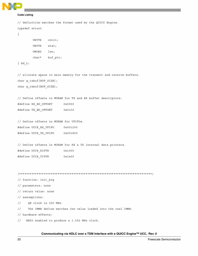
typedef struct
{
UBYTE cntrl;
UBYTE stat;
UWORD len;
char* buf_ptr;
} bd_t;
// allocate space in main memory for the transmit and receive buffers.
char g_txbuf[BUF_SIZE];
char g_rxbuf[BUF_SIZE];
// Define offsets in MURAM for TX and RX buffer descriptors.
#define RX_BD_OFFSET 0x0000
#define TX_BD_OFFSET 0x0100
// Define offsets in MURAM for VFIFOs.
#define UCC8_RX_VFIFO 0x001200
#define UCC8_TX_VFIFO 0x001800
// Define offsets in MURAM for RX & TX internal data pointers.
#define UCC8_RIPTR 0x1000
#define UCC8_TIPTR 0x1a00
/****************************************************************************/
// function: init_brg
// parameters: none
// return value: none
// assumptions:
// QE clock is 250 MHz.
// The IMMR define matches the value loaded into the real IMMR.
// hardware effects:
// BRG3 enabled to produce a 1.552 MHz clock.
Communicating via HDLC over a TDM Interface with a QUICC Engine™ UCC, Rev. 0
Freescale Semiconductor 21
Code Listing
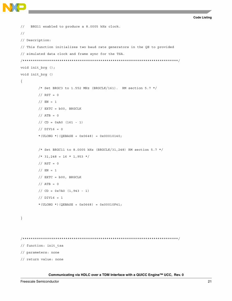
// BRG11 enabled to produce a 8.0005 kHz clock.
//
// Description:
// This function initializes two baud rate generators in the QE to provided
// simulated data clock and frame sync for the TSA.
/****************************************************************************/
void init_brg ();
void init_brg ()
{
/* Set BRGC3 to 1.552 MHz (BRGCLK/161). RM section 5.7 */
// RST = 0
// EN = 1
// EXTC = b00, BRGCLK
// ATB = 0
// CD = 0xA0 (161 - 1)
// DIV16 = 0
*(ULONG *)(QEBASE + 0x0648) = 0x00010140;
/* Set BRGC11 to 8.0005 kHz (BRGCLK/31,248) RM section 5.7 */
/* 31,248 = 16 * 1,953 */
// RST = 0
// EN = 1
// EXTC = b00, BRGCLK
// ATB = 0
// CD = 0x7A0 (1,943 - 1)
// DIV16 = 1
*(ULONG *)(QEBASE + 0x0668) = 0x00010F41;
}
/****************************************************************************/
// function: init_tsa
// parameters: none
// return value: none
Communicating via HDLC over a TDM Interface with a QUICC Engine™ UCC, Rev. 0
22 Freescale Semiconductor
Code Listing
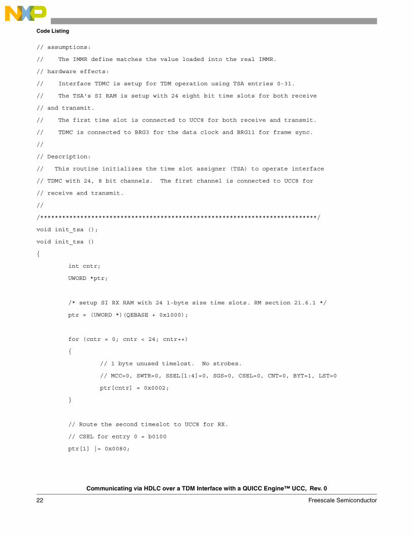
// assumptions:
// The IMMR define matches the value loaded into the real IMMR.
// hardware effects:
// Interface TDMC is setup for TDM operation using TSA entries 0-31.
// The TSA's SI RAM is setup with 24 eight bit time slots for both receive
// and transmit.
// The first time slot is connected to UCC8 for both receive and transmit.
// TDMC is connected to BRG3 for the data clock and BRG11 for frame sync.
//
// Description:
// This routine initializes the time slot assigner (TSA) to operate interface
// TDMC with 24, 8 bit channels. The first channel is connected to UCC8 for
// receive and transmit.
//
/****************************************************************************/
void init_tsa ();
void init_tsa ()
{
int cntr;
UWORD *ptr;
/* setup SI RX RAM with 24 1-byte size time slots. RM section 21.6.1 */
ptr = (UWORD *)(QEBASE + 0x1000);
for (cntr = 0; cntr < 24; cntr++)
{
// 1 byte unused timelost. No strobes.
// MCC=0, SWTR=0, SSEL[1:4]=0, SGS=0, CSEL=0, CNT=0, BYT=1, LST=0
ptr[cntr] = 0x0002;
}
// Route the second timeslot to UCC8 for RX.
// CSEL for entry 0 = b0100
ptr[1] |= 0x0080;

Communicating via HDLC over a TDM Interface with a QUICC Engine™ UCC, Rev. 0
Freescale Semiconductor 23
Code Listing
// Set the last bit on timeslot 24
ptr[23] |= 0x0001;
/* setup SI TX RAM with 24 byte size time slots*/
ptr = (UWORD *)(QEBASE + 0x1400);
for (cntr = 0; cntr < 24; cntr++)
{
// 1 byte unused timelost. No strobes.
// MCC=0, SWTR=0, SSEL[1:4]=0, SGS=0, CSEL=0, CNT=0, BYT=1, LST=0
ptr[cntr] = 0x0002;
}
// Route the second timeslot to UCC8 for TX.
// CSEL for entry 0 = b0100
ptr[1] |= 0x0082;
/* Set the last bit on timeslot 24 */
ptr[23] |= 0x0001;
/* setup SI mode register for TDM C. RM section 21.6.4 */
// SAD = 0, use entries 0-31.
// SDM = b11, internal loopback.
// RFSD = b00, No delay between sync and data.
// CRT = 1, common RX/TX clock & sync
// SL = 0, sync is active high.
// CE = 1, TX on falling edge, RX on rising edge.
// FE = 1, sample sync on rising edge.
// GM = 0, no grant mode.
// TFSD = b00, No delay between sync and data.
*(UWORD *)(QEBASE + 0x0704) = 0x0C58;
/* setup clocks in QE mux, CMXSI1CRL. RM Section 5.5.2 */
// RTC1CS = b001, TDMC RX clock is BRG3
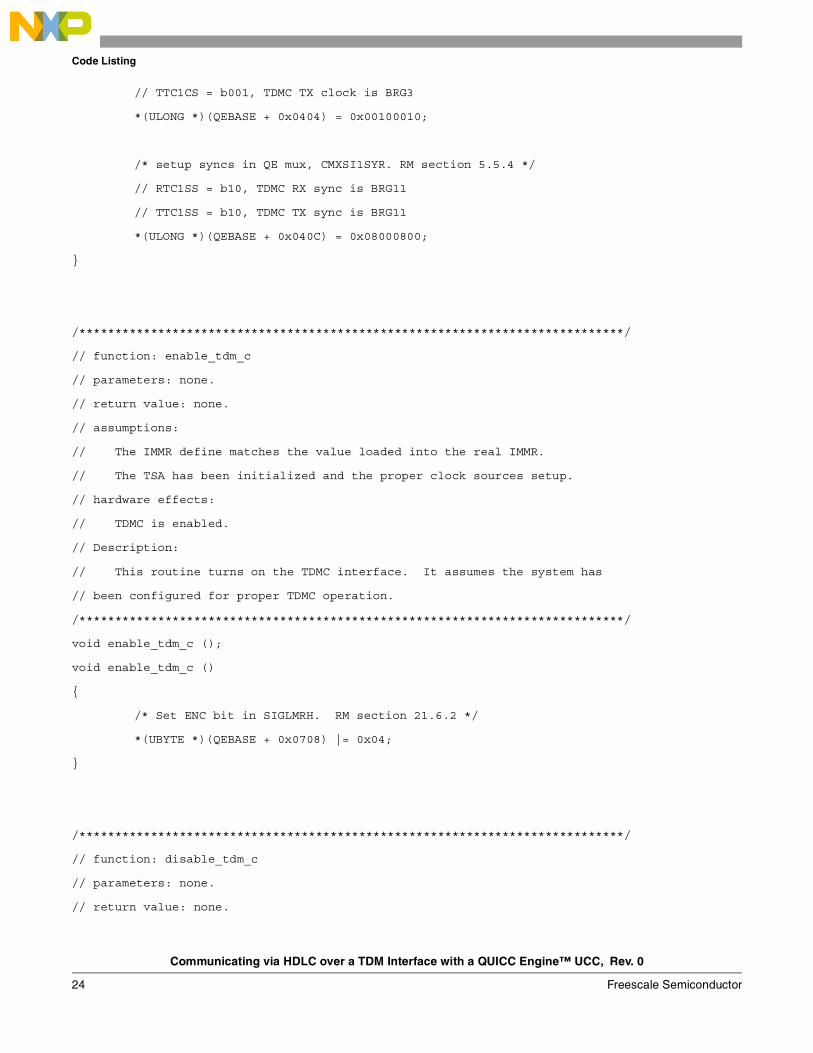
Communicating via HDLC over a TDM Interface with a QUICC Engine™ UCC, Rev. 0
24 Freescale Semiconductor
Code Listing
// TTC1CS = b001, TDMC TX clock is BRG3
*(ULONG *)(QEBASE + 0x0404) = 0x00100010;
/* setup syncs in QE mux, CMXSI1SYR. RM section 5.5.4 */
// RTC1SS = b10, TDMC RX sync is BRG11
// TTC1SS = b10, TDMC TX sync is BRG11
*(ULONG *)(QEBASE + 0x040C) = 0x08000800;
}
/****************************************************************************/
// function: enable_tdm_c
// parameters: none.
// return value: none.
// assumptions:
// The IMMR define matches the value loaded into the real IMMR.
// The TSA has been initialized and the proper clock sources setup.
// hardware effects:
// TDMC is enabled.
// Description:
// This routine turns on the TDMC interface. It assumes the system has
// been configured for proper TDMC operation.
/****************************************************************************/
void enable_tdm_c ();
void enable_tdm_c ()
{
/* Set ENC bit in SIGLMRH. RM section 21.6.2 */
*(UBYTE *)(QEBASE + 0x0708) |= 0x04;
}
/****************************************************************************/
// function: disable_tdm_c
// parameters: none.
// return value: none.

Communicating via HDLC over a TDM Interface with a QUICC Engine™ UCC, Rev. 0
Freescale Semiconductor 25
Code Listing
// assumptions:
// The IMMR define matches the value loaded into the real IMMR.
// hardware effects:
// TDMC is disabled.
// Description:
// This routine turns off the TDMC interface.
/****************************************************************************/
void disable_tdm_c ();
void disable_tdm_c ()
{
/* Clear ENC bit in SIGLMRH. RM section 21.6.2 */
*(UBYTE *)(QEBASE + 0x0708) &= ~(0x04);
}
/****************************************************************************/
// function: init_ucc8_hdlc_pram
// parameters: none.
// return value: none.
// assumptions:
// The IMMR define matches the value loaded into the real IMMR.
// hardware effects:
// UCC8's PRAM is loaded with values appropriate for HDLC operation.
// Description:
// This routine initializes the parameter RAM (PRAM) for UCC8. It is
// configured with the values for HDLC mode.
/****************************************************************************/
void init_ucc8_hdlc_pram ();
void init_ucc8_hdlc_pram ()
{
int i; // Loop counter
// first, clear 256 bytes of UCC8 PRAM. RM section 14.2.2.1
for (i = 0; i < 0x100; i++)
{
((UBYTE *)(UCC8_PRAM))[i] = 0;

Communicating via HDLC over a TDM Interface with a QUICC Engine™ UCC, Rev. 0
26 Freescale Semiconductor
Code Listing
}
// Set RIPTR & TIPTR to point to MURAM as defined by the programmer.
*(UWORD *)(UCC8_PRAM + 0x00) = UCC8_RIPTR;
*(UWORD *)(UCC8_PRAM + 0x02) = UCC8_TIPTR;
// Set MRBLR to the size of the RX and TX buffers.
*(UWORD *)(UCC8_PRAM + 0x06) = BUF_SIZE;
// Set RBASE and TBASE to point to RX and TX BDs in MURAM
*(ULONG *)(UCC8_PRAM + 0x0C) = MURAMBASE + RX_BD_OFFSET;
*(ULONG *)(UCC8_PRAM + 0x1C) = MURAMBASE + TX_BD_OFFSET;
// Set RSTATE & TSTATE. The high 8 bits of these registers are RBMR
// and TBMR. All other bits must be cleared
// RBMR and TBMR are set as follows:
// GBL = 0, snooping disabled (should be set when cache is enabled).
// BO = b10, big endian byte ordering
// CETM = 0, not used
// DTB = BDB = 0; buffers and buffer descriptors on CSB
*(ULONG *)(UCC8_PRAM + 0x08) = 0x10000000;
*(ULONG *)(UCC8_PRAM + 0x18) = 0x10000000;
// Set C_MASK & C_PRES for 16 bit CRC. Defined in RM section 14.2.2.1
*(ULONG *)(UCC8_PRAM + 0x44) = 0x0000F0B8;
*(ULONG *)(UCC8_PRAM + 0x48) = 0x0000FFFF;
// Clear DISFC, CRCEC, ABTSC & NMARC
// Note that these steps are shown for completeness. They could be
// skipped due to the clear at the start of this routine.
*(ULONG*)(UCC8_PRAM + 0x4C) = 0x0000;
*(ULONG*)(UCC8_PRAM + 0x4E) = 0x0000;
*(ULONG*)(UCC8_PRAM + 0x50) = 0x0000;
*(ULONG*)(UCC8_PRAM + 0x52) = 0x0000;
Communicating via HDLC over a TDM Interface with a QUICC Engine™ UCC, Rev. 0
Freescale Semiconductor 27
Code Listing
// Set RFTHR & RFCNT
*(UWORD *)(UCC8_PRAM + 0x5A) = 0x0001;
*(UWORD *)(UCC8_PRAM + 0x5C) = 0x0001;
// Set MFLR
*(UWORD *)(UCC8_PRAM + 0x58) = BUF_SIZE;
}
/****************************************************************************/
// function: init_ucc8_hdlc
// parameters: none.
// return value: none.
// assumptions:
// The IMMR define matches the value loaded into the real IMMR.
// hardware effects:
//
// Description:
//
/****************************************************************************/
void init_ucc8_hdlc ();
void init_ucc8_hdlc ()
{
bd_t *bd_ptr; // buffer descriptor pointer.
ULONG *cecr_ptr; // pointer to the QE command register.
int i; // loop counter.
// Connect UCC8 to TDM C by setting UC8 in CMXUCR4. RM section 5.5.8
*(ULONG *)(QEBASE + 0x041C) = 0x00004000;
// Setup GUEMR to configure UCC8 for FAST mode on both TX and RX
// note that bit 3 is reserved and must be set. RM section 6.3.2.
*(UBYTE *)(UCC8_BASE + 0x90) = 0x13;
// Setup virtual FIFOs. RM section 7.5

Communicating via HDLC over a TDM Interface with a QUICC Engine™ UCC, Rev. 0
28 Freescale Semiconductor
Code Listing
*(ULONG *)(UCC8_BASE + 0x20) = UCC8_RX_VFIFO; // RX VFIFO base
*(UWORD *)(UCC8_BASE + 0x24) = 0x080; // RX VFIFO size
*(UWORD *)(UCC8_BASE + 0x28) = 0x40; // URFET = 1/2 size
*(UWORD *)(UCC8_BASE + 0x2A) = 0x20; // URFET = 1/4 size
*(ULONG *)(UCC8_BASE + 0x2C) = UCC8_TX_VFIFO; // TX VFIFO base
*(UWORD *)(UCC8_BASE + 0x30) = 0x080; // TX VFIFO size
*(UWORD *)(UCC8_BASE + 0x34) = 0x40; // UTFET = 1/2 size
*(UWORD *)(UCC8_BASE + 0x38) = 0x20; // UTFTT = 1/4 size
// Set UCC8's GUMR. RM section 7.4.2.1
// DIAG = b00, normal mode.
// TCI = 0, normal, non-inverted clock.
// TRX = 0, normal, no transparent receiver.
// TTX = 0, normal, no transparent transmitter.
// CDP = 0, normal/envelope; must be used with HDLC in TSA mode.
// CTSP = 1, pulse mode must be used with the TSA.
// CDS = 1, synchronous mode must be used with the TSA.
// CTSS = 1, synchronous mode must be used with the TSA.
// TXSY = 0, no synchronization between RX & TX.
// RSYN = 0, normal; RX sync timing adjust only used with transparent RX
// SYNL = b00, use external sync.
// RTSM = 1, Send flags/syncs between frames
// RENC = b00, NRZ decode for RX.
// REVD = 0, normal bit order.
// TENC = b00, NRZ decode for TX.
// TCRC = b00, CRC selection for transparent TX mode only.
// ENR = 0, disabled for now.
// ENT = 0, disabled for now.
// MODE = b0000, HDLC mode
*(ULONG *)(UCC8_BASE + 0x00) = 0x03802000;
// Setup HDLC Mode Register (UPSMR). RM section 14.2.2.2
// NOF = b0000, no flags.
// FSE = 0, normal operation.

Communicating via HDLC over a TDM Interface with a QUICC Engine™ UCC, Rev. 0
Freescale Semiconductor 29
Code Listing
// MFF = 1, multiple frames allowed in transmit FIFO.
// RTE = 0, no retransmission.
// TS = 0, normal, no timestamp in RX buffer.
// BUS = 0, normal (not HDLC bus mode).
// BRM = 0, ignored in non bus mode.
// DRT = 0, normal RX operation.
// NBO = b00, normal operation (1 bit of data per clock).
// CW = b000, ignored in non bus mode.
// CRC = b00, 16 bit HDCL CRC.
*(ULONG *)(UCC8_BASE + 0x04) = 0x04000000;
// Set UDSR (data sync) to 0x7E7E. RM section 7.4.5
*(UWORD *)(UCC8_BASE + 0x0C) = 0x7E7E; // two HDLC flags
// Init PRAM for an HDLC channel.
init_ucc8_hdlc_pram ();
// Setup a single RX BD in MURAM. RM section 14.2.2.3
// First, set local pointer to RX BD in MURAM
bd_ptr = (bd_t *) (MURAMBASE + RX_BD_OFFSET);
bd_ptr->cntrl = 0xB0; // Set Empty & Int & Wrap bits.
bd_ptr->stat = 0x00; // Clear the status bits.
bd_ptr->len = 0x0000; // Clear the length.
bd_ptr->buf_ptr = g_rxbuf; // Set the data pointer to the RX buffer.
// Setup a single TX BD in MURAM. RM section 14.2.2.4
// First, set local pointer to TX BD in MURAM
bd_ptr = (bd_t *) (MURAMBASE + TX_BD_OFFSET);
bd_ptr->cntrl = 0x2C; // Set Last, Wrap, Transmit CRC */
bd_ptr->stat = 0x00; // Clear status
bd_ptr->len = 0x0000; // Clear length.

Communicating via HDLC over a TDM Interface with a QUICC Engine™ UCC, Rev. 0
30 Freescale Semiconductor
Code Listing
bd_ptr->buf_ptr = g_txbuf; // Set the data pointer to the TX buffer.
// Send an INIT RX & TX Command to the QUICC Engine. This causes
// the QE to initialize all internal data structures as per the
// programmed registers and PRAM.
i = 0; // clear the local loop counter.
cecr_ptr = (ULONG *)(QEBASE + 0x0100); // point to the QE command reg.
*cecr_ptr = 0x02E10000; // UCC8 HDLC Init RX&TX. RM Section 4.3.1
// Wait for the QE to indicate it is ready for a new command.
while ((*cecr_ptr & 0x00010000) == 0x00010000)
{
// Increment the loop counter. Production code should abort if
// the QE doesn't clear FLG after an appropriate amount of time.
i++;
}
}
/****************************************************************************/
// function: enable_ucc8
// parameters: none.
// return value: none.
// assumptions:
// The IMMR define matches the value loaded into the real IMMR.
// UCC8 registers, data structures and related hardware are
// initialized and ready to be enabled.
// hardware effects:
// UCC8's receiver and transmitter are enabled.
// Description:
// Enable RX (ENR) and Enable TX (ENT) are set in the GUMR for UCC8,
// thus allowing UCC8 to receive and transmit.
//
/****************************************************************************/
Communicating via HDLC over a TDM Interface with a QUICC Engine™ UCC, Rev. 0
Freescale Semiconductor 31
Code Listing
void enable_ucc8 ();
void enable_ucc8 ()
{
// Set ENR and ENT in UCC8's GUMR. RM section 7.4.2.1
*(ULONG *)(UCC8_BASE + 0x00) |= 0x00000030;
}
/****************************************************************************/
// function: disble_ucc8
// parameters: none.
// return value: none.
// assumptions:
// The IMMR define matches the value loaded into the real IMMR.
// hardware effects:
// UCC8's receiver and transmitter are disabled.
// Description:
// Enable RX (ENR) and Enable TX (ENT) are cleared in the GUMR for UCC8,
// thus stopping UCC8 reception and transmission.
//
/****************************************************************************/
void disable_ucc8 ();
void disable_ucc8 ()
{
// Clear ENR and ENT in UCC8's GUMR. RM section 7.4.2.1
*(ULONG *)(UCC8_BASE + 0x00) &= ~(0x00000030);
}
/****************************************************************************/
// function: main.
// parameters: none.
// return value: none (does not return).
// assumptions:
Communicating via HDLC over a TDM Interface with a QUICC Engine™ UCC, Rev. 0
32 Freescale Semiconductor
Code Listing
// The IMMR define matches the value loaded into the real IMMR.
// hardware effects:
// Configures and enables the BRGs, TSA and UCC8 using TDMC in loopback
// mode. Transmission and reception are started using the first
// timeslot.
// Description:
// This drives the entire demonstration. It first sets up the BRGs to
// provide clocks to the TDM interface that simulate T1 clocks, then
// configures TDMC on the time slot assigner to connect the first timeslot
// to UCC8, initializes UCC8 for HDLC mode, configures a transmit buffer
// to transmit continuously, enables the hardware, and then waits for
// received data to display.
//
/****************************************************************************/
void main()
{
int i=0; // Local counter.
ULONG *ucce_p = (ULONG *)(UCC8_BASE + 0x10); // pointer to UCC8 UCCE
bd_t *tx_bd_p; // pointer to TX bd
bd_t *rx_bd_p; // pointer to RX bd
// First, initialize and enable the baud rate generators used for this
// demo. In a production application, parallel port pin assignments need
// to be done at this time.
init_brg ();
// Setup the time slot assigner hardware. This routine creates
// 24 one byte time slots (similar to a T1 line). The first timeslot
// is routed to UCC8. The TSA is not enabled yet.
init_tsa ();
// Setup UCC8 and its parameter RAM for HDLC operation. UCC8 is not
// enabled yet.
init_ucc8_hdlc ();

Communicating via HDLC over a TDM Interface with a QUICC Engine™ UCC, Rev. 0
Freescale Semiconductor 33
Code Listing
// Set the RX BD pointer to the area of MURAM used to hold RX BDs. Note
// that this matches the values loaded into UCC8's PRAM RX BD pointer.
rx_bd_p = (bd_t *) (MURAMBASE + RX_BD_OFFSET);
// Set the TX BD pointer to the are of MURAM used to hold TX BDs. Note
// that this matches the values loaded into UCC8's PRAM TX BD pointer.
tx_bd_p = (bd_t *) (MURAMBASE + TX_BD_OFFSET);
// Load the TX buffer in main memory with test data.
strcpy (g_txbuf,
"Now is the time for all good men to come to the aid of the party.");
// Set the length field in the TX BD to the size of the test data.
tx_bd_p->len = (unsigned short) (strlen(g_txbuf) + 1);
// Make sure the UCC8 Event Register is clear.
*ucce_p = 0xFFFFFFFF;
// The TX BD and data are ready to transmit, so set R bit in TX BD.
tx_bd_p->cntrl |= 0x80;
// Set continuous bit in TX BD so the test data is continuously sent.
// To test a single transmission, don't set this bit.
tx_bd_p->cntrl |= 0x02;
// Clear out the RX buffer
for (i=0; i< BUF_SIZE; i++)
g_rxbuf[i]=0;
// Now that the TX and RX buffers and BDs are ready and all hardware is
// configured, enable the TDM and UCC.
enable_tdm_c ();
enable_ucc8 ();

Communicating via HDLC over a TDM Interface with a QUICC Engine™ UCC, Rev. 0
34 Freescale Semiconductor
Code Listing
// Enter an endless loop to wait for an receive frame by polling the
// RXF bit in the UCC8 Event register.
// A production application would most likely enable an interrupt for
// this event to allow the system to do other work.
while (1) {
while ((*ucce_p & 0x00080000) == 0)
{
// do nothing...
}
// Display the received data.
printf ("RX Frame: %s\n\r", g_rxbuf);
// Clear RXF Flag to allow a new event to be detected.
*ucce_p = 0x00080000;
// Clear out the RX buffer.
for (i=0; i< BUF_SIZE; i++)
g_rxbuf[i]=0;
// Set the empty bit in the RX BD to allow another frame to
// be received.
rx_bd_p->cntrl |= 0x80;
}
}
Communicating via HDLC over a TDM Interface with a QUICC Engine™ UCC, Rev. 0
Freescale Semiconductor 35
Code Listing
THIS PAGE INTENTIONALLY LEFT BLANK

Document Number: AN4026Rev. 012/2009
Information in this document is provided solely to enable system and software
implementers to use Freescale Semiconductor products. There are no express or
implied copyright licenses granted hereunder to design or fabricate any integrated
circuits or integrated circuits based on the information in this document.
Freescale Semiconductor reserves the right to make changes without further notice to
any products herein. Freescale Semiconductor makes no warranty, representation or
guarantee regarding the suitability of its products for any particular purpose, nor does
Freescale Semiconductor assume any liability arising out of the application or use of
any product or circuit, and specifically disclaims any and all liability, including without
limitation consequential or incidental damages. “Typical” parameters which may be
provided in Freescale Semiconductor data sheets and/or specifications can and do
vary in different applications and actual performance may vary over time. All operating
parameters, including “Typicals” must be validated for each customer application by
customer’s technical experts. Freescale Semiconductor does not convey any license
under its patent rights nor the rights of others. Freescale Semiconductor products are
not designed, intended, or authorized for use as components in systems intended for
surgical implant into the body, or other applications intended to support or sustain life,
or for any other application in which the failure of the Freescale Semiconductor product
could create a situation where personal injury or death may occur. Should Buyer
purchase or use Freescale Semiconductor products for any such unintended or
unauthorized application, Buyer shall indemnify and hold Freescale Semiconductor
and its officers, employees, subsidiaries, affiliates, and distributors harmless against all
claims, costs, damages, and expenses, and reasonable attorney fees arising out of,
directly or indirectly, any claim of personal injury or death associated with such
unintended or unauthorized use, even if such claim alleges that Freescale
Semiconductor was negligent regarding the design or manufacture of the part.
How to Reach Us:
Home Page: www.freescale.com
Web Support: http://www.freescale.com/support
USA/Europe or Locations Not Listed: Freescale Semiconductor, Inc.Technical Information Center, EL5162100 East Elliot Road Tempe, Arizona 85284 1-800-521-6274 or+1-480-768-2130www.freescale.com/support
Europe, Middle East, and Africa:Freescale Halbleiter Deutschland GmbHTechnical Information CenterSchatzbogen 781829 Muenchen, Germany+44 1296 380 456 (English) +46 8 52200080 (English)+49 89 92103 559 (German)+33 1 69 35 48 48 (French) www.freescale.com/support
Japan: Freescale Semiconductor Japan Ltd. HeadquartersARCO Tower 15F1-8-1, Shimo-Meguro, Meguro-ku Tokyo 153-0064Japan 0120 191014 or+81 3 5437 [email protected]
Asia/Pacific: Freescale Semiconductor China Ltd. Exchange Building 23FNo. 118 Jianguo RoadChaoyang DistrictBeijing 100022China+86 10 5879 [email protected]
For Literature Requests Only:Freescale Semiconductor
Literature Distribution Center 1-800 441-2447 or+1-303-675-2140Fax: +1-303-675-2150LDCForFreescaleSemiconductor
@hibbertgroup.com
Freescale and the Freescale logo are trademarks or registered trademarks of Freescale Semiconductor, Inc. in the U.S. and other countries. All other product or service names are the property of their respective owners. The Power Architecture and Power.org word marks and the Power and Power.org logos and related marks are trademarks and service marks licensed by Power.org.
© Freescale Semiconductor, Inc., 2009. All rights reserved.