colour television training manualcncms.com.au/.../crt-television/c25pp86n/c25pp86n_tm.pdfpin 37 of...
TRANSCRIPT

.
COLOUR TELEVISIONTRAINING MANUAL
FILE NO.
Chassis Series AAI-A
CIRCUIT DESCRIPTIONBLOCK DIAGRAM OF IcsTROUBLE SHOOTING
REFERENCE NO. TI 520004

Table of ContentslJ
Part 1 Chassis Description
1. Circuit Function Description ....................................................................................................3-52. CPU ..........................................................................................................................................6.l9
2-1 A-D Key Identification ........................................................................................ ..................... ............82-2 Option Switches .......................................................... ............................... ......... .......... ............ ....9.lO2-3 System Switch Output ............................. ........................................................................ ............l 1-122-4 Chroma lD .................................................. ................... .. .......... .............. .........................................l32-5 ldent .............. ........................ .................................. ............ ................................. .............................l32-6 Sync. lD ........ ....................................................................................................................................l4
2-7 IPC BUS .., . . . . . . . . . . . . . . . . . . . . . . . . . . . . . . . . . . . . . . . . . . . . . . . . . . . . . . . . . .. . . . . . . . . . . . . . . . . . . . . . . . . . . . . . . . . . . . . . . . . . . . . . . . . . . . . . . . . . . . . . . . . . . . . . . . .... .... 14
2-8 Band Switching ................................................................ .......................... ............ .......... .................l52-9 Tuning & Digital AFT .................................... ...................... ............ .............................................l6.l72-1o Power & Protect ........................................................ .................................... ............ ......................l82-11 Horiz./Vert. Pulse .... ....................................................................................................... .................l9
3. System Switches ...................................................................................................................20-243-1 Sound Carrier Trap ..................................... ............................ ............ ............................. .................223-2 SIF Filtering ......... ............................................................................... ............................... ...............233-3 Chroma Crystal Selection ....................................... ......... ........................ .......................... ...............24
4. External/Internal Source Selection ...........................................................................................255. lF/Video/Chroma/Def. ................................................................................................................26
6. Audio Circuit .........................................................................................................................27-296-1 Monaural Circuit .......................................................................... ...................... ...............................276-2 A2 Stereo Circuit .................. ................... ... ......................................................... ............ .................286-3 A2 Stereo & Nicam Circuit .. ................. .... ... ................... ......... ........................ ................... ...............29
7. Double/Full-wave Rectifier Circuit ............................................................................................30
Part 2 Block Diagram of ICS
1. TDA8361 /8362 .dF/Video/Chroma/Def Iect ion> ........................................................................32
2. TDA4661/V2 <1 H Delay> ............................................................................................................33
3. TDA8395 cSECAM Decoder> ..m..mm.............................................................................................344. LA7833 <Vertical Output> ..m......................................................................................................345. TDA2546A/V4 <SIF Decoder> ...................................................................................................356, MC44131 PB <Audio Multiple Decoder> ...................................................................................357, TDA8204 cNICAM Decoder> .....................................................................................................368. TDA8205 <NICAM QSPK Demodulator> ..................................................................................37
9, TDA7263M <Audio Output> ......................................................................................................38
10. STR81 145A <Double/Full-wave Rectifier Switch> ................................................................38
Part 3 Trouble Shooting Chart
1. Dead .......................................................................................................................................4l-442. No picture/No sound .................................................................................................................453. No picture-sound OK .................................................................................................................464. No sound-picture OK (Stereo model) .................................................................................47.485. No sound-picture OK (Monaural model) ..................................................................................496. No colour ....................................................................................................................................50
7. Incorrect colour phase ..............................................................................................................51
8. No vertical deflection ................................................................................................................52
-2-AA1-A

Part 1 Chassis Description
1. Circuit Function DescriptionThe following figure shows a block diagram of the AA1-A chassis.
1
%
REAR FRONT
-3-AA1-A

1. POWER SUPPLYThe power supply circuit of the AAl -A chassiscomprises a primary rectifier smoothing circuit,an oscillation circuit, a control circuit and anoutput rectifier circuit.The AC input voltage is rectified at the double orfull-wave rectifier smoothing circuit, and anunstable DC voltage is generated at bothterminals of the smoothing capacitor C307. Thedouble or full-wave rectifier circuit is build byswitching the triac on or off in IC501<STR81145A>. This voltage is supplied to theoscillation circuit, which is composed of ablocking oscillator circuit that switches theswitching transistor Q313 ON and OFF.A square-wave oscillation is generated in theinput winding according to operation of thecontrol circuit. A square-wave with amplitudedependent on the turns ratio of the input andoutput windings is obtained in the output winding.This is rectified in the output rectifier circuit, andthe desired DC voltage is produced.
2. IF& DEFLECTION (TDA8361/8362)The IF output signal from the tuner passesthrough the SAW filter, and it is inputted into pins45 and 46 of IC101.Within the IC, the IF signal passes through the IFamplifier, video detection and video amplifiercircuits, and is outputted from pin 7 as acomposite video signal.In the monaural model, this composite videosignal passes through the 5.5 MHz(B/G)/6. 0MHz(l)/6.5MHz( D/K)/ 4.5 MHz(M) soundbandpass filtering circuit, and it is inputted intopin5 of IC101. In the stereo model, the SIF signalis supplied from pin 14 of IC181 <TDA2546A> topin 5 of IC101 through the sound bandpasscircuit for modulation of the main carrier. In theIC101, this sound IF signal passes through theSIF amplifier, FM detector, external audio switchand audio output circuit, and it is then outputtedfrom pin 50 as audio drive signal (Monauralmodel). In the stereo model, the main audiosignal is fed from pinl to the stereo controller IC(MC44131PB).The video signals applied to pins 13 or 15 areseparated into vertical- and horizontal-sync.signals respectively by the sync. separator in theIc.The horizontal oscillator requires no externalcomponents and is fully integrated. This
oscillator is always running when the start-pin 36 –is supplied with 8V, and the horizontal drivesignal is outputted from pin 37. VR401 is usedfor horizontal centring adjustment.The separated vertical sync. signal from thesync. separation circuit passes through thevertical-separation circuit, and is applied totrigger divider circuit.The horizontal oscillation pulse and vertical sync.pulse are monitored by the trigger divider circuitto select either the 50Hz or 60Hz system, andautomatically adjust the vertical amplitude.The output signal from the trigger divider triggersthe vertical oscillator circuit whose externaltiming components consist of R402, C401 to pin42, and the vertical ramp signal is outputted frompin 43. VR451 is for controlling the amount of ACfeedback applied to pin 41 for adjustment of the _vertical amplitude.
3. VIDEO CHROMA (TDA8361/8362)The composite video signal output from the pin 7of IC101, passes through Q122, and the soundtraps X124, X125, X126, X127 to reject thesound carrier components, is then supplied to pin13 through the equalizing circuit consisting ofQ1 35, Q132 and Q134. The external video signalfrom SCART or other AV terminals is supplied topin 15.The video signal input to pin 13 or pin 15 isseparated into luminance (Y) signal and chromasignal in IC1 01. These pins are also common tothe H/V-sync. separation circuit input alreadydescribed.The peaking of Y signal is adjusted by DC _
voltage on pin 14.( ’’SHARPNESS” control)The chroma signal is divided into R-Y and B-Ychroma signals, which are demodulated andoutput from pin 30 (R-Y) and pin 31 (B-Y). Thesechroma signals pass through the 1H delay linecircuit (IC270), and are re-inputted at pin 29 (R-Y) and pin 28 (B-Y). These R-Y/B-Y signals passthrough the RGB matrix circuit and the RGBselector circuit of IC101. The internal RGBsignals are generated in the RGB matrix circuitand the RGB selector, consisting of linearamplifiers, clamps and selects either the internalRGB signals or the external RGB signals inputfrom pin 22 (R) , pin 23 (G), pin 24 (B). Selectionis controlled by the voltage at the RGB switchcontrol (pin 21) and mixed RGB modes arepossible since the RGB switching is fast.
—
-4-AA1-A

The RGB switch also functions as a fast blankingpin by blanking the RGB output stages; hereinternal and external RGB signals are overruled.The RGB signals for the on-screen display aresuperimposed onto the selected RGB signals atthe base of transistors Q21O, Q211 and Q212respectively.The saturation of colour gain is controlled by theDC voltage of pin 26. (“COLOUR” control)The contrast control voltage present at pin 25,controls the RGB signal gain, and the brightnesscontrol voltage present at pin 17, controls DClevel of RGB signals.The RGB signals are finally buffered beforebeing presented to the RGB output pins [pin 20(R), pin 19 (G), pin 18 (B)].
4. AUDIO OUTPUT4-1 (AN5265)-Monaural modelThe audio signal output from pin 50 of IC101 isinputted to pin 2 of ICI 71 and passes throughthe pre-amplifier circuit and the drive circuit intothe audio amplifier. The audio amplifier is theSEPP (Single-Ended Push Pull) type and theoutput from pin 8 drives the speaker directly.
4-2 (TDA7263M)-Stereo modelThe audio signals output from pins 17 and 18 ofIC1l 01 (MC44131 PB) are inputted to pins 1(Left)and 5( Right) of IC1 102 and passes through thepre-amplifier circuit and drive circuit, after whichit is input to the audio amplifier. The audioamplifier is the SEPP (single-ended, push-pull)OTL type and the outputs from pins 8( Right) and10(Left) drive the speakers directly.
5. VERTICAL OUTPUTAn LA7833 is used for the vertical output circuitin this chassis. The vertical ramp signal from pin43 of IC101 is inputted to pin 4 of IC451. Thisramp drives IC451, and vertical scanning isperformed. In the first half of scanning adeflecting current is outputted from pin 2 andpasses through the following path:VCC(B4)+D451+ pin 3+ pin 2+ DY+ C461+
vR451/R459.An electric charge is then stored in C461. [n thelast half of scanning the current path is:C461+ DY+ pin 2+ pin 1+ VR451/R459 +
C461In this way, an increasingcurrent flows directly to
sawtooth waveformthe DY to perform
electron beam deflection. During the first half ofthe blanking period the vertical ramp signalsuddenly turns OFF. Since there is no longer anycurrent flowing into the DY, the magnetic fieldcollapses causing an induced current to flow asfollows:DY+ pin 2+ pin 1+ VR451/R459+ C461 + DY
Once the magnetic field in DY has dissipated,the current path becomes:Vcc+ pin 6+ pin 7+ C452+ pin 3+ pin 2 +DY+ C461 + VR451/R459
and when the prescribed current value isreached, the vertical drive ramp signal turns ON.This completes one cycle.
6. HORIZONTAL OUTPUTThe horizontal oscillation signal is outputted frompin 37 of IC101 and used to switch the drivetransistor Q431. This switching signal is currentamplified by the drive transformer T431 anddrives the output transistor Q432. When Q432turns ON, an increasing current flows directly tothe DY throughC441/C442+ L441/R441 + DY+ Q432-C +
Q432-Eand the deflection occurs during the last half ofthe scanning period. When Q432 turns OFF, themagnetic field stored in the DY up to that pointcauses a resonant current to flow into thecapacitors C420 and C423 and charges them.The current stored in C420 and C423 then flowsback to the DY causing an opposite magneticfield to be stored in the DY. This field thencollapses increasing a current which switchesthe dumper diode in Q432 ON. The resonancestate is completed, and an increasing currentthen flows again directly to the DY through thedumper diode.By this means, the deflection in the first half ofthe scanning period is performed. When Q432turns ON at the end of the first half of thescanning period, the deflection during the lasthalf is begun, thus completing one cycle.
In the PCC circuit consisting of Q461 and Q462,the parabola signal supplied from the verticalcircuit is added at the horizontal output stage andpincushion compensation is performed byvarying the DC bias. Further, the ABL voltage isfedback to the base of Q462 to compensate forwidth variations due to variations in the beamcurrent.
-5-AAI -A

2. CPU
The following figure shows a block diagram of the CPU peripheral circuit.
!7-—. —-— -’
il !I
I
0 acu.
—.—. —
—-—. — .
acu
-6-AA1-A

The following table shows pin descriptions of the CPU.
Pin Description Pin Description
1 Horizontal sync. signal input 27 +5V power supply2 Vertical sync. signal input 28 Oscillator 2 for OSD3 Volume control output 29 Oscillator 1 for OSD4 Colour control output 30 Reset input5 Brightness control output 31 Detection power failure (Error: Lo)6 Contrast control output 32 AV2 option switch (Hi: AV2)7 Sharpness control output 33 Option switch (System selection)8 Tnt control output 34 Key scan input (DV)9 AV1/AV2 switch output (AV1 :Low) 35 Key scan input (DC)
10 TV/AV switch output (TV: Hi) 36 Option input & SIF output D/K11 AFT S-signal input 37 Option input & SIF output I12 ipc bus SCL line 38 Option input & SIF output B/G13 12C bus S(JA line 39 Option input & SIF output M/M14 Tuning voltage output 40 System switch output SECAM15 Ident signal input 41 System switch output 3.5816 RC signal input 42 System switch output 4.4317 --- 43 Band switch output I (Low: VH)18 Chroma ID input 44 Band switch output II (Low: VL)
19 Ignore signal input 45 AC switch off detection input
20 Sync. ID input 46 Option switch (RC status)21 --- 47 Sound mute output (Mute on:Low)22 GND 48 Power on/off output (P-On: Hi)23 GND 49 Blanking signal output for OSD24 Oscillator input for CPU 50 OSD blue signal output25 Oscillator output for CPU 51 OSD green signal output26 GND 52 OSD red signal output
-7-AAI-A

2-1 A-D Key Identification Circuit
The key identification circuit used in this chassis uses a switched resistive ladder network in
an A-D conversion circuit to generate and send a voltage to the CPU when a key is pressed.The CPU uses this voltage to determine which key was pressed. This resistive circuit
eliminates the need for encoder/decoder devices, simplifying design and adding to the
reliability of the TV.
The table shows the voltages input to CPU pin 34 and 35, when a given key is pressed.
QK1 5“ SW
CPU
35 4
34 +
47kzizEa47k
[:115’ K3 &o 15’
6.8k K’ Kll6.8’
— —
4.7’ K5 ~24.7’
—
2.7’ K6 K13 2.7’— —
1.8’ ~7 K14 1.8’— —
1.5’ K8 K15 1.5’— —
$150
Inputvoltageto pin 35
I Kev I ● flangeofvolta9es I Function
OFFK1K2K3K4K5K6K7KR
lessthan0.6V0.6V- 1.2V1.2V- 1.8V1.8V- 2.4V2.4V- 3.OV3.OV- 3.7V3.7V- 4.3V4.3V- 4.9V
morethan4.9V
NoKeyPos.+Pos.-vol.+(TuSlow)Vol.-(Tu Slow)FunctionPreseUMemoryColourSystemSIFSvstem
i10k
Input voltage to pin 34-,
Key ● RangeofVoltages Function
OFF lessthan0.6V 60prog.positionsSw 0.6V- 1.2V 30prog.positionsK9 1.2V- 1.8V TVIAVK1O 1.8V-J2.4V n/aKll 2.4V--3.OV nlaK12 3.OV- 3.7V nlaK13 3.7V- 4.3V nlaK14 4.3V- 4.9V nlaK15 morethan4.9V nla
● When the supply voltage is 5.oV.
AA1-A
-8-AA1-A
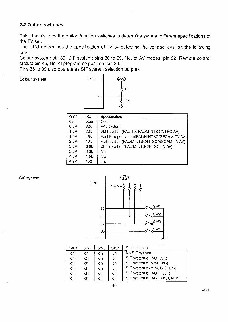
2-2 Option switches
This chassis uses the option function switches to determine several different specifications of
the TV set.The CPU determines the specification of TV by detecting the voltage level on the followingpins.Colour system: pin 33, SIF system: pins 36 to 39, No. of AV modes: pin 32, Remote controlstatus: pin 46, No. of programme position: pin 34.Pins 36 to 39 also operate as SIF system selection outputs.
Colour system
rPinll
Ov0.5V1.2V1.8V2.5V3.OV3.8V4.3V4.9V
SIF system
rSwlononoffoffonoff
--13CPU 5
Rx
33
10k
Rxopen82k33k18k10k
6.8k
3.3k
1.5k
150
SpecificationTestPAL systemVMT system(PAL-TV, PAL/M-NTST/NTSC-AV)East Europe system(PAL/N-NTSC/S ECAM-TV,AV)Multi system(PAUM-NTSC/NTSC/SECAM-TV,AV)China system(PAUM-NTSC/NTSC-TV,AV)nlanlanla
CPU10kx4
39
38
37
36
ILSW2 SW3 SW4on on onoff on offoff on onoff on offoff off offoff off off
-9-
SpecificationNo SIF systemSIF system e (B/G, D/K)SIF system d (M/M, B/G)SIF system c (M/M, B/G, D/K)SIF system b (B/G, 1,D/K)SIF system a (B/G, D/K, 1,M/M)
AAl -A

AV modes
CPU10k
32 -“9
Remote control status
CPU
46P-5
10k
9
No. of programme position
7’5
CPU
d
HSw
Rx=47k+15k+6.8k+4.7k+2.7k+l .8k+l .5k+150
34
10k
SW5 Specificationoff 2 AV system (AV1/AV2)
I on 11 AV system (AV)I
SW6 Specificationoff w/o remote control functionon w/ remote control function
Sw Specificationoff 60 programme positionson 30 programme positions
AAl A
-10-AA1-A

2-3 System switch output
The outputs from pins 40 to 42 of the CPU select the colour system and the outputs from pins36 to 39 the SIF system. These outputs drive the colour and SIF system switching circuits.The operation of each switching circuit is shown in the tables below.
Colour system sw.
v
I SECAM
I NTSC
thing output
Output pins
42 41 40
HHL
HLL
HLH
LHL
Display
Auto
PAL/NTsc4.43
SECAM
NTSC
SIF system switching output
1. Multi system(SIF system a option)
SIF system
Auto
B/G-5 .5MHz
I-6.OMHZ
D/K-6 .5MHz
M/M-4 .5MHz
Output pins
39 38 37 36● HHH
LHLL
LLHL
LLLH
HLLL
Display
S1
S2
S3
S4
S5
● It depends on receiving TV system
2.3 system (SIF system b option)
~
B/G-5 .5MHz I input H LL
I-6.OMHZ input L HL
D/K-6 .5MHz input L LH
Display
S1
S2
S3
S4
3. China, PX (SIF system c option)
SIF system Output pins Display
39 38 37 36
Auto● H input H S1
BIH-5.5MHZ LH input L S2
DIK-6.5MHz LL input H S3
MIM-4.5MHZ HL input L S4
● Itdepends on receiving TV system
-11-AA1-A

4. Indonesia (SIF system d option)
SIF system Output pins Display
39 38 37 36
Auto ● H input input S1
BIG-5 .5MHZ LH input input S2
MIM-4.5MHZ HL input input S3
5. East Europe (SIF system e option)
SIF system I Output pins I Display
I 39 38 37 36 IAuto input H input H S1
B/G-5 .5MHz input H input L S2
D/K-6 .5MHz input L input H S3
6. No SIF system
SIF system Output pins Display
39 38 37 36---- input input input input
AA1-A
AAl A
—
-12-

2-4 Chroma ID
The identification of a colour or black/white broadcast is achieved by sensing the voltage
level input at pin 18. This voltage is supplied from pin 26 of ICI 01 through the inverter circuit,
Q771. When there is a black/white broadcast the voltage on pin 26 goes low.
Normally, pin 26 operates as colour control function, and the control voltage is from pin 4 ofthe CPU.To identify the colour system during a black/white broadcast, the CPU judges that the system
is NTSC when the following conditions are detected at same time.(1) The colour system is “AUTO” or “NTSC” system.(2) The field frequency is 60 Hz.(3) TV/AV mode is “TV” mode.
CPU
18CHROMA ID
btE!zzd4
COLOUR
R77310k
R774220k
4 R77512k
1 “T
U....................................i Colour control~ D/A circuit ~....................................
ICI 01Chroma/Def.
26COLOUR
2-5 Ident (Identification)
The identification of the receiving signal status is done by the CPU sensing the voltage levelat the input pin 15, as shown below. The ident signal is presented at pin 4 of IC101 and fed topin 15 of the CPU through the converter circuit consisting of Q700, R706 and R722.When the CPU judges that the system is 4.43MHz, it outputs a “Low” signal from pin 39 toselect the PAUSECAM system.
CPU
IDENT 15
4.5 MHZ 39
012V IICI 01Chroma/Def.
,
Pin39 Pin15 Judgement Signal status
L O-1.8V 4.43 MHZ No sync.
H 1.8V - 4.3V 3.58 MHz Signal present
L 4.3 v - 5.OV 4.43 MHZ Signal present AA1-A
AAl -A
-13-

—
2-6 Sync. ID
When no signal is received the voltage on pin 14 of IC101 changes to “Low”. As aconsequence, D783 and Q718 are turned on, and a “High” is supplied to pin 20 of the CPU.As a result, the CPU judges that no signal is being received. In the AV mode, the CPUoutputs a “High” signal from pin 51 to drive the blue back function.
CPU
SYNC. ID 20
E!zE5E9SHARPNESS 7
Q718
a
R7855.6k
IclolChroma/Def.
14 SHARPNESS
:4.......................................
—; Sharpness control~ D/A circuit. ...................................... L
2-7 Bus control
This chassis uses the IPC bus as the interface for operation control between ICS, and theCPU is used as the master for operation control of the Teletext decoder, A2 Stereo decoder,Nicam decoder and Memory IC.The IPC bus is composed of the SCL(Serial Clock Line) and SDA(Serial Data Line) lines.Data is transmitted over the SDA line in 8-bit units in synchronisation with the SCL line.These lines are also used for the option function. When the TV set turns on, the CPU oncesends the slave address of the Teletext IC, Nicam IC and Stereo IC via the SDA line andwaits the ACK(Acknowledge) signal from each IC.The CPU judges which decoder is available by receiving the ACK signal.
CPU
SCL 12
SDA 13
R7463.9k
d
IC790Memory IC
6 SCL
5 SDA
AAl -A .
AA1-A

2-8 Band switching circuit
The band switching control signals are outputted from pins 43and440f the CPUand fed tothe base of Q781, Q782 and Q784, band switching transistors.The one of these transistors then outputs the drive voltage(+l 2V) to the tuner according tooutput signal as shown below table.When the UHF band is selected, “High” signal are sent from both pins 43 and 44. The D781and D782 are cut off, then Q784 and Q783 are turned on and +12V is supplied to UHFterminal on the tuner.
Antenna
L
Tuner
VI-
VH
u
s-Q781
44.7k
0782
4,7k
Q7834
Q784
* ---
Band Switching Logic
output1
Pin43 Pin44 I Q781 Q782 Q783 I Selected Band
H L on off off VHF-Low
L H off on off VHF-High
H H off off on UHF
44 Band II
43 Band I
CPU
AAl -A
-15-AA1-A

2-9 Tuning and Digital AFT
The tuning system of this chassis also utilises a digital AFT system.
In this operation, the tuner is automatically adjusted to the required tuning point of the
broadcast signal by increasing and decreasing the tuning voltage within the synchronisation
range, whilst checking the 2 signals from the lF/Video decoder IC, ICI 01 <TDA8361/8362>.The signals which are outputted from pins 4 and 44 of IC101 are fed to pins 15 and 11 of theCPU via the impedance and voltage converler circuit.The CPU checks the voltage level of the Ident signal at pin 15 and the AFT-S signal at pin
11, and controls the tuning voltage which is supplied to the tuner.
The CPU determines that the correct tuning point is achieved when the Ident signal is Hi(5V)and the AFT-S signal is between 2.OV to 3.OV.When the Ident signal is Hi(5V) and AFT-S signal is greater than 3.OV, the CPU judges thatthe tuning point is incorrect and increases the tuning voltage output from pin 14 of CPU tocorrect the tuning point.When the Ident signal is Hi(5V) and AFT-S signal is less than 2.OV, the CPU again judges –
that the tuning point is incorrect and decreases the tuning voltage output from pin 14 of CPUto correct the tuning point.The CPU always maintains the correct tuning point by monitoring these two signals.
-16-AA1-A

/ CPU Iclol
Tuner (k lF&VIDEO
Q700 R767100
Q711 w , 4 IDENT(T.B.)IDENT IN
TU 14 15; ;;:’ ; :.;324
TUNING OUTI
z
R7065.6k
C746 R7220.01 10k
\ R121R123
68k“Ok
I w 44 AFT
z :.;:$
AFTIN 11 4R780150k \
Input Signal
Pin 11 AFT S-Curveof IC701 Input
Pin 14of IC701
Pin 15of IC701
Tuning Voltage
IdentSignal Input
/ \ 3.5V
3.OV
2.OV, 1.5V
,:, ,,), Ov,,, ,,!. .,.
‘ Tuned point
I Imut Voltacie Level of Pin 11 I Judgement
LL(oV-1 .5V) Tuning Voltage Down
L (1.5V-2.OV) Tuning Voltage Down
M (2.O-2.5V) Tuned
H (2.5V-3.OV) Tuning Voltage Up
HH(3.5V-5V) Tunina Voltaue Up
-17-AA1-A

2-10 Power On/stand-by and Protection circuit
Power On/Stand-by
The power on/stand-by signal is outputted from pin 48 of CPU.When the stand-by mode is selected the voltage of pin 48 changes from Hi(5V) toLow(OV), which turns Q792 off and Q793 on. Q793 drives the photo-coupler D315 which inturn drives Q312 on. Finally Q312 stops the oscillation of power circuit switching the TVinto the stand-by condition.At the same time, Q793 drives the LED, D1120 to illuminate and indicate the stand-bymode.
Protection circuit
A protection circuit is provided to protect the TV set in case of a circuit malfunction.When an abnormality occurs during TV reception it causes pin 31 of the CPU to gocontinually Low (less than 2.OV). After one second, the CPU detects that a power failurehas occurred on the TV set, and the CPU turns the TV into the stand-by condition.
CPU
POWER 48
31PROTECT IN
K\) —.J.
... —-. —,. . . . . . . . . . . . . . .
.
..
.
,. I
PowerOscillationCircuit
Q312
\5viZiiZ’iJStand-By ,V—.. — . . j_—.. —..
.................................. 1
95V D362 D363 10V
I I
11‘“fF%@ ‘i ~lj\ / .................................,.................................f -“”””””’~m~ii6 ~-= ~:!~~:rmer~
7,......................: ..-
...Jormal
iPower failure ‘“” """"""""""""""c`J""""""""""""""""""'""""--"""""""""""-
operation ................................... Ov ~ D468 &! ................................1<:LL
-.. —.. —..l —
MI-A —-
-18-AAI -A

2-11 Horiz./Vert. pulse input
The vertical and horizontal pulse from the deflection circuits are inputted to pins 1 and 2 inorder to synchronise the On Screen Display.The vertical pulse inputted to pin 2 is made by the sandcastle pulse which is outputted frompin 38 of ICI 01. The sandcastle pulse is extracted the horizontal components at the CRintegrating circuit consisting of R796 and C791.The horizontal pulse inputted to pin 1 is made by the retrace pulse which is generated on pin5 of flyback transformer.If one of these pulses is not supplied to the CPU, the on-screen display cannot be displayed.
-1u’1 EYHoriz. 4111111111111111111111111
CPU
H-SYNC. 1
V-SYNC. 2 I
\
IL---Aw
Hor]z,
JVeri.
IclollF/Video/Chroma
38
AA1-A
-19-AAI -A

3.System switches
The following diagram shows the multi system, selection circuit of this chassis.The description on the following page, describe these switches which are controlled by IC701(CPU) output.
NTSCBand Limitter
5●
101 (TDA8362
F in V ir
TV 011[
HUE
SECAMREF.
;IF in
CHROMA IE
IDENT(Time Base
13 :
NHf’ {
..$3 W8j u3-
. . . . .. . .. . . . . . . . . . . . . . . . .
6.OMHZ Filter +5-%S9(Q155)
5.5 MHz Filter J-c%S8(Q154)
.4,5 MHz Filter +h-
SIF Filter S7(Q152)
1“””’””””””””-””--/S2
R=
lE
1:
42
41.......
. . . . ; I
+ ........(Q203) ; IC280
(SECAM)
>’ ..................z+.............................................. ......................
IC701(CPU) :
-’o”’IDENT 4.5 3g------.--.o;5:.-
5.5 .38..-.-.--.-----; 1Go 37 ;
::$.43 65 36. ; ~
::::~
3.58 :!:!
50/60 ID ,:/:::::
2 :::
;;:,,:....................................................
........................................................
:
.....
_ V-SYNC. Pulse(for OSD)
AA1-A
AAl-A
-20-

The system switches (S1 -S1 O) are used for multi-standard model.(Refer to the block diagram of system switching circuit on previous page)
SI :
S2:
S3:
S4 :
S5 :
S6:
S7:
S8:
S9:
Switch for band-limiting on NTSC(3.58) mode (Dl 06)This switch is driven by ON/OFF signal from CPU (pin39).Switch for sound carrier trap on NTSC(3.58) mode (Dl 20)This switch is driven by signal from CPU (pin39).Switch for sound carrier trap except NTSC(3.58) mode (D I 21 )This switch is driven by inverting signal from CPU (pin39).System switch for forced SECAM mode (Q203)This switch is driven by ON/OFF signal from CPU (pin40).System switch for forced 4.43 mode (Q222)This switch is driven by ON/OFF signal from CPU (pin43).Note: When the colour system is set to “AUTO”, both S6 and S7 will turn on.
System switch for forced 3.58 mode (Q221 )This switch is driven by ON/OFF signal from CPU (pin42).System switch for 4.5 MHz filtering on NTSC(3.58) mode (Ql 52)This switch is driven by ON/OFF signal from CPU (pin39).System switch for 5.5 MHz filtering on B/G mode (Ql 54)This switch is driven by ON/OFF signal from CPU (pin38).System switch for 6.OMHZ filtering on I mode (Ql 55)This switch is driven by ON/OFF signal from CPU (pin37).
S1O: System switch for 6.5 MHz filtering on D/K mode (QI 56)This switch is driven by ON/OFF signal from CPU (pin36).Note: When the TV system is set to “AUTO”, S7, S8, S9 and S1 O will turn on.
-21-AA1-A

3-1 Sound Carrier Trap Circuit
When the 4.5 MHz system is selected, the CPU outputs a “High” signal from pin 39. Q153 isturned on and Q157 is turned off. As a result D121/Dl 23 are cut off and D120 is turned on.The composite video signal from pin 7 of IC101 is supplied to the base of Q135 via the4.5 MHz trap circuit Xl 25 which removes the intercarrier sound content. From the equalizingcircuit the CVBS video signal is fed to pin 13 of IC1 01. When other systems are selected thecomposite video signal is fed through the 5.5 MHz/6 .0 MHz trap X126, or the 6.5 MHz trapXl 27, which remove the respective intercarrier sound contents. The remaining video is fed topin 13 of IC101 via the video equalizing circuit to compensate the characteristic of video .This switching is shown in the table be~ow.
CVBS in 13
IclollF/Video/chroma
CVBS out 7
CPU
4.5 MHZ 39
...........................-. —- —_ — _________________ :
d II I: Video
C216 ~~ Equalizing0.1 I: :$;;,
L124 i ~ g;;;j
X124R137 ‘1
R14 :.......
4“Jp
5.5 MHz 27k220 R138
1’– —- —DJ=-— 150 —.m .->’
~w K ‘—.—- X125. . R139 ~126 4.5 MHZ,*,
R134100
lk Q122 D121
‘w ‘
D123R149 R148680 680
X126
w
5.516 .OMHZ
X127I 6.5 MHz
R1581.8k
R19527k
R15633k
SIF System Pin 39 Q153 Q157 D120 D121
4.5 MHZ H On off On off
Other I L IIoff I On on On
-22-AA1-A
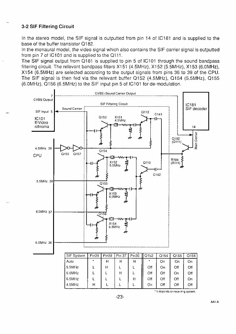
3-2 SIF Filtering Circuit
In the stereo model, the SIF signal is outputted from pin 14 of IC181 and is supplied to thebase of the buffer transistor Q1 82.In the monaural model, the video signal which also contains the SIF carrier signal is outputtedfrom pin 7 of IC101 and is supplied to the Qlll.The SIF signal output from Q181 is supplied to pin 5 of IC101 through the sound bandpassfiltering circuit. The relevant bandpass filters Xl 51 (4.5 MHz), Xl 52 (5.5 MHz), Xl 53 (6.OMHZ),Xl 54 (6.5MHz) are selected according to the output signals from pins 36 to 39 of the CPU.The SIF signal is then fed via the relevant buffer Q152 (4.5 MHz), Q154 (5.5 MHz), Q155(6.OMHZ), Q156 (6.5MHz) to the SIF input pin 5 of IC101 for de-modulation.
7CVBS Output
SIF Input 5
IclolIf/Video/chroma
4.5 MHZ 39
CPU
5.5 MHZ 3[
6.OMHZ 37
6.5 MHz 36
CVBS+Sound Carrier Outwt i
Q153 0157
SIF Filterina Circuit....................................................................................................
0112C141
ni~? X1514.5 MHZ
E-w
F
+111-www-f
.........................................................................................................................................................,
IC181Sound Carrier SIF decoder
4
14
IQ154 - I
~
Q-fII F-Ji X1546.5 MHz
TSIF System Pin39
Auto ●
5.5 MHZ L
6.OMHZ L
6.5 MHz L
4.5 MHZ H
Pin38
H
H
L
L
L TPin 37 Pin36
H H
L L
H L
L H
L L
-23-
‘4k.............. ,_
Q182k8(Qlll) c.—
2
3R184:Rlll)
Q152 Q154 Q155 Q156* On On On
off On off off
off off On off
off off off On
On off off off
‘ It dependson receiving system,
AA1-A
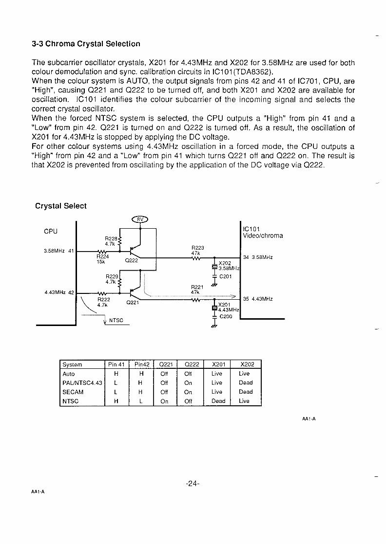
3-3 Chroma Crystal Selection
—
The subcarrier oscillator crystals, X201 for 4.43 MHz and X202 for 3.58 MHz are used for bothcolour demodulation and sync. calibration circuits in IC101 (TDA8362).When the colour system is AUTO, the output signals from pins 42 and 41 of IC701, CPU, are“High”, causing Q221 and Q222 to be turned off, and both X201 and X202 are available foroscillation. IC101 identifies the colour subcarrier of the incoming signal and selects thecorrect crystal oscillator.When the forced NTSC system is selected, the CPU outputs a “High” from pin 41 and a“Low” from pin 42. Q221 is turned on and Q222 is turned off. As a result, the oscillation ofX201 for 4.43 MHz is stopped by applying the DC voltage.For other colour systems using 4.43 MHz oscillation in a forced mode, the CPU outputs a“High” from pin 42 and a “Low” from pin 41 which turns Q221 off and Q222 on. The result isthat X202 is prevented from oscillating by the application of the DC voltage via Q222.
Crystal Select
CPUR2284.7k
3.58MI+z 41R223
VvvR224
47k
15k Q222 Vvv1 X202
? 3“58MH’i 1
I1,= ,,,_’- ,
4 JIR2294.7k
4.43 MHz 42 1 47k.Vv ...... .... . . . . . . . . . . . . . .... .....>
\
R222 Vvv4.7k Q221 1X201
~4.43MH;
I -$ N-ECL c,20f3
J-
IclolVideo/chroma
34 3.58 MHz
35 4.43 MHZ
System Pin 41 Pin42 Q221 C1222 X201 X202
Auto H H off off Live Live
PAUNTSC4.43 L H off On Live Dead
SECAM L H off On Live Dead
NTSC H L On off Dead Live
AAI-A
-24-AA1-A
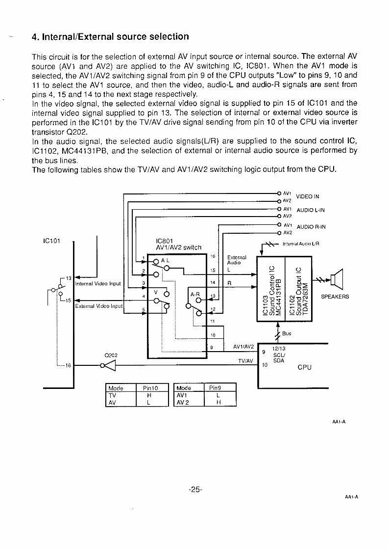
4. Internal/External source selection
This circuit is for the selection of external AV input source or internal source. The external AVsource (AV1 and AV2) are applied to the AV switching IC, IC801. When the AV1 mode isselected, the AV1/AV2 switching signal from pin 9 of the CPU outputs “Low” to pins 9, 10 and11 to select the AV1 source, and then the video, audio-L and audio-R signals are sent frompins 4, 15 and 14 to the next stage respectively.
In the video signal, the selected external video signal is supplied to pin 15 of IC101 and theinternal video signal supplied to pin 13. The selection of internal or external video source isperformed in the IC101 by the TV/AV drive signal sending from pin 10 of the CPU via invertertransistor Q202.In the audio signal, the selected audio signals(L/R) are supplied to the sound control IC,IC1l 02, MC44131 PB, and the selection of external or internal audio source is performed bythe bus lines.The following tables show the TV/AV and AV1/AV2 switching logic output from the CPU.
Iclol
–13
k
)–15
-..16
JIternal Video Input
;xternal Video Inpu
Q202
0 ~;; VIDEO IN
O AV1 AUDIO L.IN
0 AV2
~~~ ‘uD’OR-’N
IC801 \AVIIAV2 switch
4’”
Internal Audio L/R
1 16 ExternalAudio
15 L g*
53
...........14 R bm
H K&
4 SGmm;o=~3~@
{: 11;; .......~: A;:~; 10 / ; Bus
. ...................
9 AV1 IAV2 12113.......................... 9SCIJ
TVIAV SDA10
CPU
4SPEAKERS
AA1-A
-25-AA1-A

5. lF/Video/Chroma/Def. Circuit
The following figure shows a block diagram of the lF/Video/Chroma/Def IC peripheral circuits.
1-30$1
ns
mm ml
J.y.”. ----
1---nnnmu-)(i)000Zz iif
.
i
3.>-3
cd.‘=*
A A 4
1-
-26-
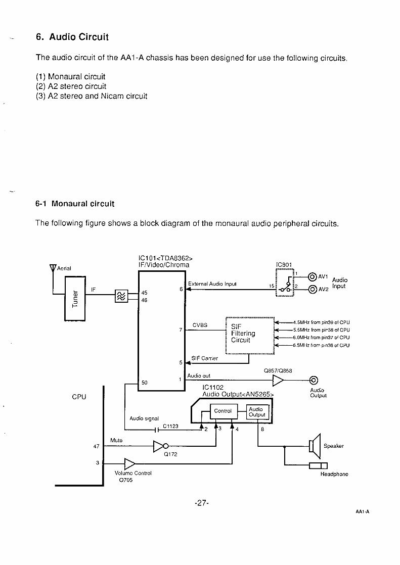
6. Audio Circuit
The audio circuit of the AA1-A chassis has been designed for use the following circuits.
(1) Monaural circuit(2) A2 stereo circuit(3) A2 stereo and Nicam circuit
6-1
The
Monaural circuit
following figure shows a block diagram of the monaural audio peripheral circuits.
CPU
—
47
3
Mute
ICI 01 <TDA8362>lF/Video/Chroma IC801
45 6
46
7
5
501
Audio signal
.,,,,,,,,,,,.
j ~Avl A.di.External Audio Input 15:
,J #-@AV2 ‘“put1............
CVBS : SIF/ 4.5MHz frompin39 of CPU
- Filtering ~5,5 MHz from pin38 of CPU
~ Circuit :- 6.OMHz from pin37 of CPU
;~6.5MHz from pin36 of CPU
. ...............”..............,,:- S1F Carrier I
Q857K?8584udio out
IC1102
Audio 0U@Jt<AN5265sAudiooutput
~1 C“23Speaker
{Vol~me Control Headphone
Q705
-27-AA1 -A

6-2 A2 stereo circuit
The following figure shows a block diagram of the A2 stereo audio peripheral circuits.
Nr.INN1111>>2>m,lno$=rLr3wul !-- I,,“ . . . . . . . . . . . . . . . . . . . . . .
IL~I-!P; “=~
E ‘zu?:_, _mu
\
7)0,9 y ~3
:9 +5Q’52<=<< 26 ......................................................................?
-lU :~
g~
m‘Q (m 2n ala ~
An%:
Lu
:
........;
E!ico 0
u-l.’=
I
qns IUy?w
/),.,,...................” . . . . . . ...”....
10(n
AA1-A
-28-

6-3 A2 stereo and Nicam circuit
The following figure shows a block diagram of the A2 stereo and Nicam audio peripheralcircuits.
~ msvvas.. . ... .. ..... ..... .. . . ..”. ”,O.,-,...”...-.”. ..”.!..
muc? L-
A...................................... .....
3ns08.=c
Z
................. .,
I
,.,,.,,.,.,.,.,............... ,.,.,....
.
I..........................,.,,.u)c.—&E“%u?—.-(00
5
........ ..........................r
A
,-
qns! I
u!ew
,.....,.,,..”..., ..................................................
.
-29-

7. Double/Full-wave rectifier circuit —
The rectifier circuit of this chassis is employed the double/full-wave rectifier switching circuitto operate the power supply circuit in stability from 90V to 290V AC input.The fig. 1 shows the double/full-wave rectifier switching circuit using the triac IC STR81145A,IC501 .The triac in the IC501 automatically switches on or off to build up the double or full-waverectifier circuit according to the input AC voltage level.In the range from 90V to 145V AC input, the double rectifier circuit is build up by switching thetriac on in the IC501 as shown in fig.2.During the positive half cycle of AC input, the current flows as follows; AC(plus)+ IC501 pin2
+ pin3 + C509 + D509 + AC(minus). The voltage is charged in C509. During the
negative half cycle, the current flows as follows; AC(minus)+ D508 + C508 + IC501 pin3 +
pin2 + AC(plus). The voltage is charged in C508. As a result, the DC voltage which is
double of AC input voltage is observed between the output terminals KG-1 and KG-2.In the range from 145V to 290V AC input, the full-wave rectifier circuit is build up by switchingthe triac off as shown in fig.3.During the positive half cycle, the current flows as follows; AC(plus) + D506 + C508/C509 +
D509 + AC(minus), and the negative half cycle, AC(minus) + D508 + C508/C509 + D507
+ AC(plUS). The voltage is charged in C508/C509. As a result, the DC voltage which is
same level of AC input voltage is observed between the output terminals KG-1 and KG-2.This circuit can be supplied the proper DC voltage to the power oscillation circuit when theAC input voltage varies in the range from 90V to 290V.
R508A ~ KG-1 ,. ............................:Q <
AC Input SW501 D506/u ~’ !Power ~
VAC VDC c307~Oscilation j:Circuit :
~KG-2 :.............................
D5012 N 3
1)R503
L
L:504 C5074IC501STR81 145A
~ Main Unit
[5:,,,.,.,,,,,,,...,.,,,,,,,,,,,,,,,,,,,,,,,,,,0,,,,
Fig.1
@iz3–Vi= VAC’@ V~c= 2*Vi--
Vi= VAC‘G VDC= Vi
+Fj;i
~ KG-1
Vi,:1
VACQ*vivw=zw
<--------------------- -------------’ -J KG-2
‘ C509 — -- —-—-J IC501
I 2/.
3 11 I1 4
on
Fig.2 Double Rectifier& Smoothing Circuit Fig.3 Full Waveform Rectifier& Smoothing Circuit
-30-AAI -A


IFlN
l—
IFlN
2—
TU
NE
AD
J+
FM
DE
1
G FM
DE
M2
IFV
O
b
Cb
4
AU
DE
M
yE
XT
AU w-l-
DE
CD
IG
4115
014
714
814
414
314
114
2I4
0I%
139
138
137
134
135
132
127
*‘
!MP
LIF
IER
%.
AG
C
I
-
:‘1
-:
*:(
‘l;~
:,~
‘“;+
’-;
ii
VE
RT
ICA
LP
HA
SE
1P
HA
SE
2X
TA
LH
UE
OU
TP
UT
OS
CIL
LAT
OR
CO
FW
RO
L
49 ~
CE
MC
OU
AT
OR
–A
FC
AN
DS
AM
PLE
VE
RT
ICA
LLI
NE
SY
ST
EM
PH
AS
E3
AN
DH
OLD
DIV
IDE
RO
SC
ILLA
TO
RT
UN
ING
MA
NA
GE
RD
ET
EC
OR
z
7
1
VID
EO
*V
IDE
O*
PO
WE
R3C
DE
KIH
FC
AT
CN
“H
AN
DV
CO
INC
IDE
NC
EA
MP
LIF
IER
RE
SE
T“
DE
TE
CT
OR
SE
PA
RA
TIO
ND
EM
OD
ULA
TO
R31
II
b-
+
1I
11
[I
1
6—
PR
EA
MP
LIF
IER
28S
WIT
CH
MU
TE
TD
A83
61N
OIS
EA
CC
*+
VO
LUM
ED
ET
EC
TO
RA
MP
LIF
IER
MA
TR
IXC
LAM
PS
2SS
ET
+
+I
II
I
51!
--
22
.LI
MIT
ER
—P
LLT
RA
PA
ND
CH
FO
dlN
AfK
E.
CH
RO
MIN
AN
CE
-LU
MIN
AN
CE
-C
LAM
P%
BY
PA
SS
BA
ND
PA
SS
MA
TR
IXS
WIT
CH
aj
+
I1
1119
Ilo5Z
1216
1315
1425
2621
17I
II
II
Ii
II
II
IL
IIR
- J-N
DE
T
)B
YO
TO
BY
OT
DA
4661
BY
l
IR
Yl;]
~~66
1
1—
RI
—G
I—
‘1
--00
+G
OL
+R
O
,1
A’
I
,tC
tiR/)
MA
~~?s
~l?s
CO
N‘
ItiR
lP
EA
KIN
GN
D2
GN
D3
“pm
mR
GB
IN
;:CC
OLO
UR

Pin description of TDA8361/8362
Pin Symbol Description
1 AUDEM2 IFDEM13 IFDEM24 IDENT5 SOIF6 EXTAU7 IFVO8 DECDIG
9 GND1
10 Vp
11 GND2
12 DECFT
13 CVBSINT
14 PEAKIN
15 CVBSEXT
16 CHROMA17 BRI18 BO19 GO20 RO21 RGBIN22 RI23 GI24 BI25 CON26 SAT
Audio de-emphasisIF demodulator tuned circuitIF demodulator tuned circuitVideo identification outputSound IF input and volume controlExternal audio inputIF video outputDecoupling digital supplyGround 1Positive supply voltage(+8V)Ground 2Decoupling filter tuningInternal CVBS inputPeaking control inputExternal CVBS inputChrominance and AV switch inputBrightness control inputB outputG outputR outputRGB insertion and blanking inputR inputG inputB inputContrast control inputSaturation control input
2. TDA4661 <IH Delay Line>
*(R-Y) + ~
colour-differenceinput signals
+( B-Y)+~
vpl —
sandcs.tie —pulse input
Pin Symbol Description
27 HUE Hue control input28 BYI B-Y input signal29 RYI R-Y input signal30 RYO R-Y output signal31 BYO B-Y output signal32 XTALOUT4.43MHZ output for TDA839533 DET34 XTAL135 XTAL236 HOSC37 HOUT38 FB1/SCO39 PH2LF40 PHI LF41 VFB42 VRAMP43 VOUT44 AFCOUT45 IFIN146 IFIN247 AGCOUT48 DECAGC
49 TUNEADJ
50 AUOUT
51 DECDEM
52 DECBG
Loop filter burst phase detecter3.58 MHz XTAL connection4.43 MHz XTAL connectionStart horizontal oscillatorHorizontal outputFlyback input.lsandcastle outputPhase 2 loop filterPhase 1 loop filterVertical feedback inputVerlical ramp generatorVertical outputAFC outputIF input 1IF input 2
Tuner AGC output
AGC decoupling capacitor
Tuner take-over adjustment
Audio output
Decoupling sound demodulator
Decoupling bandgap supply
16 SIGNAL
“ CLAMPING
-pre-amphf]ers addition
stagesoutput
14 SIGNAL“ CLAMPING
A
9* I
~ analogue supply
~~3MHzshifting clink 2-
5TDA4661 6-
. SANXASTLEFRECIJENCY 13
iITECTOR- PHASE
DETECTOR
IVP2
-33-
— +(R-Y)
mlour-differenceoutput sugnals
— *(B-Y)
- n.c.-n.c.-n.c.- n.c.
- i.e.
AA1-A

7. TDA8204 <NICAM Decoder>
Pin description of TDA8204
DAC
DAC
DL
DR
SCLSDA
Pin Symbol Description Pin Symbol Description
1 GND Ground 22 GND ground2 DACDR PWM data output (R) 23 ER Error monitor flag output3 DACDL PWM data output (L) 24 RESET Reset4 SERI Serial bus output 25 MUTE NICAM mute5 VDD +5V supply voltage 26 GND Ground6 RSW Reserve sound switch (status/control) 27 DDI De-scramble data input7 HAO Hardware address O 28 DDO De-scramble data output8 TESTO Test O 29 FID Frame identification flag output9 US2 User bit 2 input 30 PDV Parity data validity flag output
10 Usl User bit 1 output 31 ADV Additional data validity flag output11 Uso User bit Ooutput 32 VDD +5V supply voltage12 SCL Serial clock IZCbus 33 DV Data validity flag output13 SDA Serial data PC bus 34 SEL1 Language selection 1 input14 SD Serial data PC bus 35 SELO Language selection Oinput
15 SCK Serial clock IZCbus 36 TEST1 Test 1
16 WS Word select IZCbus 37 TESTO Test O
17 VDD +5V supply voltage 38 GND Ground18 C4 Application control bit 4 flag 39 NDI NICAM data input19 C3 Application control bit 3 flag 40 CK728 728kHz bit clock output20 C2 Application control bit 2 flag 41 TEST2 Test 2
21 cl Application control bit 1 flag 42 CK1 1648 11 .648 MHz bit clock input
-,
-36-AA1-A

8. TDA8205 <NICAM QPSK Demodulator>
Ii-
BGin—
TEST-
RESET—
do _lcf
Oaz -lUZ$%zzSs LZmcna
Zz-1 Uu
9 18 I1O 11 34 35 36 31 32 37 38
* ,>+AOL
* ,>
~ AOR
— DC1— DC2
I I *MMO
I I INTERFACE
TDA8205 1 III 125 113 12 13 140
h12 14 33 17 I 20
11 I> AGND XC1 XC2XK1 RG RF ILICAP SERI
Pin description of TDA8205
Pin Symbol Description Pin Symbol Description
1 AGNDI Analogue ground 1 22 CK728 728kHz clock input2 MCI Option, 13.104 MHz Xtal 23 NDO NICAM data output3 MC2 Option, 11.7MHz Xtal 24 TEST Test4 DF2 Data filter 2 (eye monitor) 25 MMO Matrix mute output5 DF1 Data filter 2 (eye monitor) 26 AGND2 Analogue ground 26 BGIN System BG input 27 ADL Audio output (left)
7 IIN System I input 28 ADR Audio output (right)
8 AGC AGC filter condenser 29 DC1 De-coupling 1
9 VCC2 +12V supply voltage 30 DC2 De-coupling 2
10 AVDD +5V supply voltage 31 AMOL Audio mute output (left)
11 LFIL1 Filter 1 left (J-17 de-emphasis) 32 AMOR Audio mute output (right)
12 RG Gain adjust resistor (DAC) 33 CAP De-coupling condenser13 AGND3 Analogue ground 3 34 MAI Monaural audio input14 RFIL1 Filter 1 right (J-17 de-emphasis) 35 SAIL Stereo audio input (left)15 RESET Reset 36 SAIR Stereo audio input (right)16 VDD +5V supply voltage 37 EAIL External audio input (left)17 SERI Serial bus input 38 EAIR External audio input (right)18 DACDL DAC data input (left) 39 Vccl +12V supply voltage19 DACDR DAC data input (Right) 40 XK1 11.648MHz Xtal20 DGND Digital ground 41 LF2 Loop filter 221 CK1 1648 11.648MHz clock output 42 LF2 Loop filter 1
-37-AAI-A

9. TDA7263M <Audio Output>
IN -L 1
IN +L—
SUPPLY _VOLTAGE
IN +R--
IN -R -
21 L
10+
3MUTE
1
-REFERENCES . ,
t
9 TURN-ONAND-OFF E
ScPROTECTION
Tj
THPROTECTION
5
4 8
I 1
16 ~ RF1 27K TDA7263M
OUT L
CF “COUPL
10. STR811 45A <Double/Full-wave Rectifier Switch>
2 1k 3
Triac4
rl
Z2
Z1
QI Q3
5 STR81145A
Pin Function1 Delay2 TI3 T24 Gate5 Common
-38-AA1-A

(
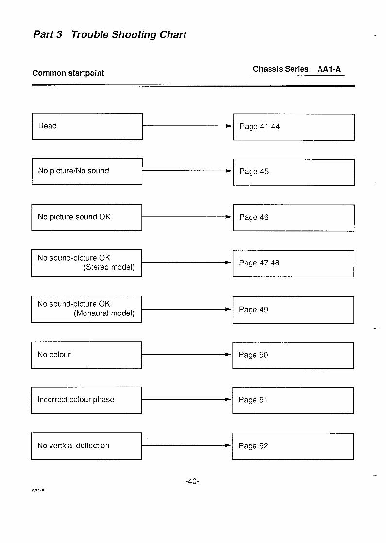
Part 3 Trouble Shooting Chart
Common startpointChassis Series AAI-A
Dead w Page 41-44
No picture/No sound > Page 45
1 1 )
No picture-sound OK~ ‘age4’
I I 1
No sound-picture OK b(Stereo model)
Page 47-48
No sound-picture OK(Monaural model)
b Page 49
I I 1
No colour
“~
Incorrect colour phase
“~
No vertical deflection
“~
-40-

Trouble Shooting Chart Startpoint symptom: Dead
~
No Check Power primary circuitIs the fuse OK ? Q313, Q312, L312, D311, D315,
PS501 , R503, D501 , IC501 ,
Yes C501 , C502, C307, C315
v
Check voltage on both ends of Ov Check Power primaty circuit
C307 - SW501 , L501 A, F501 , R508A,R512A, IC501, AC CordI
I250V-400V
vCheck voltage on both ends of OvC521 w
1OV-20V
T501 , D521 -D524, C521
Check voltage on pin 27 of IC7014
IC701 , Q521 , R523, D526,C522, C729, C721 , C722,
L I1 I A1101, L703
I+5V
Observe voltage B2(+24V) on bothends of C365 when turning on TVset with RC transmitter.The voltage rise up to 10V-24V onceand then fall down to OVimmediately.
I Yes
It operates protection circuit
Go to next page
No●
Check Power primary circuitQ313, Q312, Q311, C317,R324, R320, R321 , R322, T311 ,D315, C314, R319Check stand-by circuitQ792, Q793, D361 , R792, IC701
-41-AAl -A

Trouble Shooting Chart Startpoint symptom: Dead
I.-----------------------------------------rI Disconnect power failure detection diodes, ~ Caution:
~ D362, D393, D433, D468, D486II Do not keep TV set on more than 5 seconds duringI
IL ; the following check otherwise the TV set may has a---- ---------------- -------------- --------
[
damage.
keep disconnection and check as follow
Check voltage on pin 31 of IC101F
I 5V
IC701, R776 or detection circuit
v
Ov IC701 , R792, Q792, Q793,Check voltage on Q353-collector P
D361
I1OV-40V
t
Check voltage B1 (+140V) on both 80V or less Short circuit on B1 line
ends of C361* D351 , C361 , Q432, C426,
D486, C1793, C1794
I80V or more
v
Check voltage B2(+24V) on Ov
terminal “KAA-3”*
I24V
t
Check voltage B4(+24V) on pin 6 ofOv
*IC451
24V
Short circuit on B2 lineD355, C365, R362, IC1102,CI103, C1111
Short circuit on B4 lineIC451 , C451 , D353, C363, R364
—
IGo to next page
-42-

Trouble Shooting Chart Startpoint symptom: Dead
Y
Check voltage B5(+15V) on pin 1(IV
bof IC351
I15V
Short circuit on B5 lineIC351 , D354, C364, R360
T
Check voltage B6(+12V) on pin 3Ov Short circuit on B6 line
* IC351, C371, IC181, A101,of IC351
IC801, IC1103, C101, C114,412V C117, C180, C190, C733, C801,
vI C1172
Check voltage B7(+8V) on pin 3 ofIC352
,18V
Check waveform on pin 37 of IC101
Yes
v
Check waveform on Q431 -collector
w
OvShori circuit on B7 lineIC352, IC101 , IC280, R368,C372, C407, C406, Cl 37, Cl 36,D215, C283, C282
L1m Iv
Horiz.
‘: ICIO1 , D214, R408, R409,X201 , X202
n 1
N 50”
Horiz.
‘) Q431 , R431, C431 , C432,C434, R434, T431
v
Check voltage on both ends ofOv
* Check horizontal output circuitC421 Q432, L431 , C420, R422, DY,
1 C421 , D432, R449
I5V or more
Go to next page
-43-

Trouble Shooting Chart Startpoint symptom: Dead
vCheck voltage on both ends of 5V or less Check CRT heater circuit
C469 + T471 , R481 , R475, D467, C469I I I
10V or more
YOv
Check voltage on terminal “KB-l” - D485, C488, R485, T471
1
I180V
R476, D363, R776
AA1-A
-44-

Trouble Shooting Chart Startpoint symptom: No picture/No sound
~
------- ------- ------------------No :
1I
Is CRT heater lighting ? >! Go to chart “Dead”I1
1 I1 II
I I
IYes
L---____________________J-------_J
Chick voltage(+33V) on bothOV
* R716, D704, C716ends of D704
I33V
Check tuning circuit
Is tuning voltage changing onNO IC701 , C745, L702, R758, Q711,
>terminal TU on tuner when tuning
L706, R765, R763, R704, R705,C707, C708, Cl 05, X701, R755,
Yes OV to 33V R756, R744, R746, C781 , C782,L705
J I
1
Is supply voltage(+l 2V) observedNo VL: Q781 , R778, Cl 03
on terminal LB, HB, UB on tuner- VH: Q782, R777, Cl 04
1
UHF: Q783, Q784, R786, R787,
Yes C106
Check AGC voltage on terminalOV or 8V
>AGC on tuner
C131, R133, C130, C128
.13V-6V
OV or 8VCheck voltage on pin 49 of IC101 * VR120, R127, R126, C128
I
13V-6V
Check tuner and IF peripheralcircuitIC1O1, AIO1, QIO1, R103, C115,T121, L121, C129, C119, X1OI
-45-AAI -A

Trouble Shooting Chart Startpoint symptom: No picture-sound OK
Is video signal observed on Q1 22-emitter “ “~
IYes
Is video signal observed on Q1 35-base
Yes
vI
FI Hc)riz.
Check sound trap circuitR143, D120-D123, R138, R139,L125, L126, Xl 24-X127, R148,R149
Is video signal observed on Q1 34-l!!!!-1 No Q135, Q134, Q132, R144,
base- R140, R142, R151 , R152, L136,
C145, C147.
I*
Yes mv
Is video signal observed on pin 13of Icl 01 ‘w “~
I 1 I1
IYes
Check voltage on pin 16 of IC101“~
I OvCheck voltage on pin 17 of IC101 + C206, C712, R721 , R718
Check voltage on pin 25 of IC101
‘:~3V-7V
R231 , R232, Cl 792, R1792,R1794, C1795, R1797
-46-AA1-A

Trouble Shooting Chart Startpoint symptom: No sound-picture OK(Stereo model)
No sound-picture OK(Stereo Model)
Select correct sound system
ING
I TiiiG==Yes Check Nicam decoder peripheral
No sound on Nicam broadcast
1
Yes check AZ stereodecoderNo sound on A2 stereo broadcast - peripheral circuit
I IC1103, RI172, R1176, R1177
I1
No sound on all of broadcasts
Check voltage on pin 15 of IC701Y
Check voltage on pin 45 of IC701F
IC101 , C132, R767, C718,Q700, R706
D528, R526, C523, D527
I 4V-5V
t
Go to next page
-47-AA1-A

Trouble Shooting Chart Startpoint symptom: No sound-picture OK(stereo model)
vIlv
Check voltage on pin 3 of IC1l 02 *
Ov
IC701 , Q172, R175, R179
I I I
t l!!!!-1Yes
Check waveform on pin 1 of IC1102 * Check audio output circuitIC1102, Headphone, speakers
Check waveform on pin 3 of IC1l 03w
No
Check IC1l 03 peripheral circuitX1171, C1171, C1173, C1187,C1191, C1188, C1189
+ l.!!!!dYesCheck waveform on pin 1 of IC101 - C1179, R1183, C1183
I INo
t P!!!!-l0.3VYes
Check waveform on pin 5 of IC101 * IC101, C122, C123, C138, R125
Check waveform on pin 14 of L!!!!!-l0.3V
No
1+ SIF circuit peripheral circuit
I IC181 Q102, R108, C182, X180,
I IC181, c188, C186, T181, T181 I
1YesI 4
Ch~ck SIF filterina c ircuitNo sound on 4.5 MHz------ Check Q112, Q152, X151, Q153, Q157 peripheral circuitNo sound on 5.5 MHz------ Check Qll 3, Q1 54, Xl 52 peripheral circuitNo sound on 6.OMHZ------ Check Qll 3, Q1 55, Xl 53 peripheral circuitNo sound on 6.5 MHz------ Check Q113, Q156, X154 peripheral circuitAll of systems ---------------- Check Q153, Q157, Q182, R128, C141, C142 peripheral circuit,
RB701 , IC701An
.
-40-

Trouble Shooting Chart Startpoint symptom: No sound-picture OK(Monaural model)
No sound-picture OK(Monaural Model)
Select correct sound system
NG
vw
Check voltage on pin 15 of IC701 IC101, C132, R767, C718,Q700, R706
llVIC101, Q172, R168, D528,
Check voltage on pin 3 of IC1101R526, C523, D526, R179
1
IOv
1
Check voltage on pin 4 of ICI101Ov
when maximum volume setting●
C1112, R1129, C706, R731,Q705, R708, C703
I6-8V
Check waveform on pin 2 of w
Icllol + IC1lO1, C1lO1, C1116,I Check audio output circuit
[ I1 speakers, headphone
I
i
1 I
No
Check waveform on pin 50 of m Yes
Iclol - C1117, C1123, R170I ! I
No
\ ‘~Check SIF filterina circuit
No sound on 4.5 MHz------ Check Qll 2, Q152, Xl 51, Q1 53, Q157 peripheral circuitNo sound on 5.5 MHz------ Check Q113, Q154, Xl 52 peripheral circuitNo sound on 6.0 MHz------ Check Q113, Q155, X153 peripheral circuitNo sound on 6.5 MHz------ Check Qll 3, Q156, Xl 54 peripheral circuitAll of systems ---------------- Check Qlll, R150, Rlll, C143, R116, C122, C123, C128, R125
~eri~heral circuit
-49-AA1-A

Trouble Shooting Chart Startpoint symptom: No colour
I I Yes ~
I No colour on NTSC system + Q222, X202
YesNo colour on PA1/SECAM system
*Q22’x2011
No
*-J Yes
No colour on SECAM system * IC280, C284, C285, L285,C281 , C280
1No
No colour on all of systems
OvCheck voltage on pin 1 of IC270 p IC270, C270, D275, C275,
R275, L280
tOv
Check voltage on pin 26 of IC101 - C211, R713, R715, C711 , R775,Q771
1 I
I2-6V
AAl -A
-50-

Trouble Shooting Chart Startpoint symptom: Incorrect colour phase
~1
Excessive red colour
“~
Loss or poor red colour + Q21O, R21O, D201, R1762,Q1761 , Q1762, J1703, VR1761,VR1762, C1761, R1766, R1768
Excessive green colour F ‘1773D211Q1771 , Q1772, Q211, VR1772,
Loss or poor green colourQ211, R211, D202, R1772,Q1771 , Q1772, VR1772,C1771 , R1776, R1778, J1702
Excessive blue colour F ‘R1782)D212Q1781, Q1782, Q212, VR1781 ,
Loss or poor blue colour
Incorrect colour phase on NTSC●
system only
Incorrect colour phase on all of *systems
R793, R732, R7233, R737, C715
IC270, IC280, IC101 , C204,C205, C271 , C272
-51-AAl -A

Trouble Shooting Chart Startpoint symptom: No vertical deflection
~1 11’letloriz.nhllifl~ appears on the screen
Check waveform on pin 4 ofIC451
Yes
v
IC451 , C452, DY, D471 , C461 ,R459, R455, VR451 , C456, R454,R453, R452, C464, SW220
1-llru 1“ -r‘0 iCIOl , R401 , R456, C454,
R402, C401 , C402, R403
-52-AA1-A

MEMO
-53-AA1 -A

A14800/Mayl’95/500 S1SANYO Electric Co., Ltd.Printed in Japan