coexistence of 1d and quasi-0d photoluminescence from...
TRANSCRIPT
Published: June 28, 2011
r 2011 American Chemical Society 3003 dx.doi.org/10.1021/nl201610g |Nano Lett. 2011, 11, 3003–3009
LETTER
pubs.acs.org/NanoLett
Coexistence of 1D and Quasi-0D Photoluminescence from SingleSilicon NanowiresJan Valenta,*,† Benjamin Bruhn,‡ and Jan Linnros‡
†Department of Chemical Physics & Optics, Faculty of Mathematics & Physics, Charles University in Prague, Ke Karlovu 3,121 16 Prague 2, Czechia‡Materials Physics, ICT School, Royal Institute of Technology, Electrum 229, 164 40 Kista-Stockholm, Sweden
Light-emitting properties of Si nanowires (Si-NWs) are rela-tively little explored compared to silicon quantum wells
(quasi-2D structures) and, especially, quantum dots (quasi-0Dstructures).1 However, the interest in understanding electron�hole generation and recombination in silicon nanowires has beenrapidly growing during the last years when new methods of Si-NW mass production have been introduced.2,3 Their potentialapplications include mainly novel solar cells,4�6 detectors andsensors,7 battery electrodes,8 etc. Regardless of the fabricationtechnique, luminescence characterization of grown Si-NWs ispotentially the most convenient (fast, nondestructive, andsensitive) characterization technique if properly understoodand related to structural information.
Photoluminescence (PL) of Si-NWs was addressed by severalgroups with results very similar to other Si-based nanostructures(porous and nanocrystalline Si). Namely observing broad PLspectra in the orange�red�near-IR spectral region9,10 andsometimes also blue emission11 which is often ascribed to defectsin the SiO2 shell.
12 As the most interesting observations, we canhighlight the increase of absorption cross section, the suppres-sion of Auger recombination (Auger lifetime was found to beabout 2 orders of magnitude longer compare to Si nano-crystals),13 and the very high (nearly complete) linear polariza-tion ratio of PL from Si-NWs.14 The inevitable variations of Si-NW diameter create potential traps that can act as localizationcenters for electron�hole pairs. However, the related questionon the role of delocalized 1D excitons and localized quasi-0D
excitons in the photoluminescence emission from Si-NWs wasnot resolved up to now.
In this paper we demonstrate localized emission from 0D-likequantum dot centers as well as emission from delocalized 1D-likeexcitons. Both types of emission originate from the samestructures, i.e. from nanowires made of oxidized silicon walls.The walls have been fabricated from silicon wafers using elec-tron-beam lithography, plasma etching, and by careful oxidationin the self-limiting oxidation regime.15 The distinction betweenthe two types of recombination becomes possible as the quantumdot emission is characterized by a local emission center (in theemission image captured by a CCD camera) and by a relativelysharp luminescence peak. The 1D exciton emission on the otherhand is distributed along a single nanowire and is characterizedby a broad spectrum starting at a lower energy. The broadspectrum most likely comes from thickness variation and acorresponding confinement energy variation along the nanowire.Excitons may possibly transfer from the 0D centers to 1Dnanowires in our structures, or vice versa. This would requiremore dedicated experiments and in this paper the main pointremains to prove the coexistence of the two different excitons.
The Si-NW fabrication procedure is similar to the onedescribed in a previous paper.16 Negative resist HSQ was spunonto n-type (20 Ω 3 cm resistivity) 10 � 10 mm2 Si(100) wafer
Received: May 13, 2011
ABSTRACT: Single silicon nanowires (Si-NWs) prepared by electron-beam lithography and reactive-ion etching are investigated by imagingoptical spectroscopy under variable temperatures and laser pumpingintensities. Spectral images of individual Si-NWs reveal a large variabilityof photoluminescence (PL) along a single Si-NW. The weaker broademission band asymmetrically extended to the high-energy side isinterpreted to be due to recombination of quasi-free 1D excitons whilethe brighter localized emission features (with significantly variable peakposition, width, and shape) are due to localization of electron�hole pairsin surface protrusions acting like quasi-0D centers or quantum dots(QDs). Correlated PL and scanning electron microscopy images indicatethat the efficiently emitting QDs are located at the Si-NW interface withcompletely oxidized neck of the initial Si wall. Theoretical fitting of thedelocalized PL emission band explains its broad asymmetrical band to be due to theGaussian size distribution of the Si-NWdiameterand reveals also the presence of recombination from the Si-NW excited state which can facilitate a fast capture of excitons into QDcenters.
KEYWORDS: Nanowire, quantum dot, silicon, luminescence, exciton
3004 dx.doi.org/10.1021/nl201610g |Nano Lett. 2011, 11, 3003–3009
Nano Letters LETTER
pieces at 6000 rpm and baked for 10 min at 150 �C. Line patternswere exposed using electron beam lithography (EBL), and thesample was developed in a MF-CD26 bath (1 min). HBr-basedreactive ion etching (RIE) transferred the patterns into the bulksilicon, resulting in standing silicon walls. These were thenoxidized for 30 min at 900 �C, which led to nanowire formationin the top of the wall. Si-NWs are oriented along the [100]direction.
The sample morphology was visualized using a Zeiss Geminiscanning electron microscope (SEM) at 20 kV accelerationvoltage, which enables a distinction between remaining siliconcore and oxidized parts of the walls. Cross sections of theoxidized silicon walls were performed with a FEI Nova 200focused ion beam (FIB) after deposition of first a carbon layerand then a platinum protection layer.
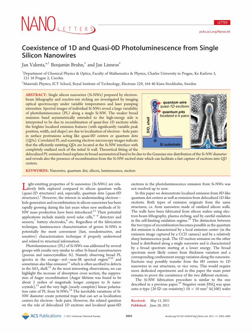
Figure 1 shows reflected (a) and PL (b)microimages of part ofthe lithography-defined structure, which contains 25 efficientlyemitting Si-NWs (about 74 μm long). These Si-NWs were usedto obtain the results presented in this paper. They are numberedstarting from the right side, as indicated in Figure 1b.
Photoluminescence microspectroscopy was performed usinga home-built setup based on an inverted microscope coupled to a30 cm imaging spectrograph with a back-thinned CCD camera.Samples were mounted on a special copper holder in a coldfingerof a cryostat (available temperature range is about 5�300 K). Asingle objective lens (40�/0.6 with correction for influence of acryostat window) was used to focus excitation light as well ascollect and image emitted signal (epifluorescence configuration).Excitation by the 405 nm diode laser was sent to a samplethrough an optical system which allowed exciting a wide field of a
sample (approximately 32 μm in diameter). The excitationpower density was variable between∼0.04 and 80 W/cm2 usingneutral density filters. Alternatively to the excitation laser, whitehalogen lamp light can be sent to the sample in order to observereflection images of the studied structures. Silicon nanowireswere oriented parallel to the spectrometer entrance slit (andparallel to the polarization of the laser excitation as the excitationefficiency is strongly polarization dependent17). Then the en-trance slit was closed to ∼0.13 mm in order to image just onesingle Si-NW and detect its spectral image (see Figure 1). Theresolution of the different emission spots within an individual Si-NW is given by the diffraction limit to about 800 nm. Typicalacquisition times for low-temperature spectral microimages arebetween 30 and 60min, therefore the position drift of a sample ina cryostat must be less than 1 μm/h. All spectra were corrected tothe spectral response of the apparatus. In the infrared part of thedetected range (see, e.g., Figures 1c and 2a�c) the back-thinnedCCD chip exhibits a strong etaloning effect. It can be correctedby appropriate correction curves and additionally by the adja-cent-points averaging. Also hot spots (see Figure 1c) are usuallycorrected (by replacing with neighbor pixel signal value) in thepresented spectra.
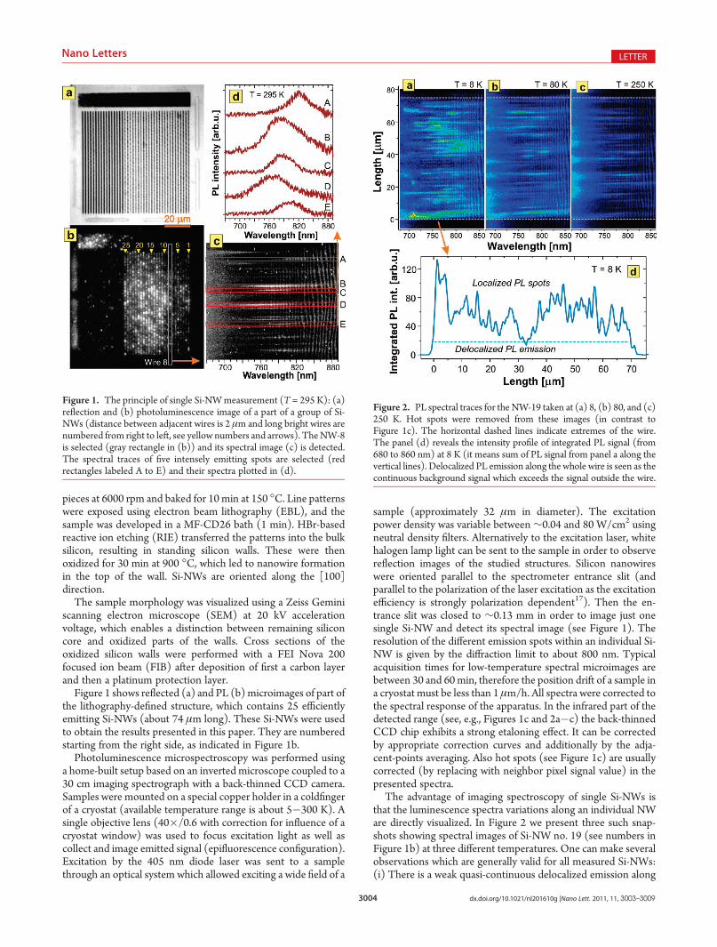
The advantage of imaging spectroscopy of single Si-NWs isthat the luminescence spectra variations along an individual NWare directly visualized. In Figure 2 we present three such snap-shots showing spectral images of Si-NW no. 19 (see numbers inFigure 1b) at three different temperatures. One can make severalobservations which are generally valid for all measured Si-NWs:(i) There is a weak quasi-continuous delocalized emission along
Figure 1. The principle of single Si-NWmeasurement (T = 295 K): (a)reflection and (b) photoluminescence image of a part of a group of Si-NWs (distance between adjacent wires is 2 μm and long bright wires arenumbered from right to left, see yellow numbers and arrows). TheNW-8is selected (gray rectangle in (b)) and its spectral image (c) is detected.The spectral traces of five intensely emitting spots are selected (redrectangles labeled A to E) and their spectra plotted in (d).
Figure 2. PL spectral traces for the NW-19 taken at (a) 8, (b) 80, and (c)250 K. Hot spots were removed from these images (in contrast toFigure 1c). The horizontal dashed lines indicate extremes of the wire.The panel (d) reveals the intensity profile of integrated PL signal (from680 to 860 nm) at 8 K (it means sum of PL signal from panel a along thevertical lines). Delocalized PL emission along the whole wire is seen as thecontinuous background signal which exceeds the signal outside the wire.

3005 dx.doi.org/10.1021/nl201610g |Nano Lett. 2011, 11, 3003–3009
Nano Letters LETTER
the whole NW which exceeds the background signal (outside aNW), especially at low temperatures (see Figure 2d whereintegrated PL intensity profile obtained from Figure 2a is pre-sented). (ii) A few points in the NWhave much stronger emissionthan the continuous signal and their spectral position and shape(number and width of emission bands) is strongly variable, (iii)these intense spectra are less abundant and somehow wider athigher temperatures (compare panels a�c in Figure 2).
In Figure 3a we compare different components of the NW-19PL signal at T = 50 K. The red line represents the overallintegrated and corrected PL spectrum (the adjacent averaging
was applied to smooth the spectrum), the blue line is the sum of alldistinguishable localized PL spot spectra (five of these localizedspectra are shown in the bottom part of Figure 3a with expandedintensity scale), and the black line is the difference of the overall andlocalized spectra. It is clear that the continuous emission exceeds thesum of localized emission by an order of magnitude (at thistemperature of 50 K) even if its brightness (intensity per unit area)is lower. When we “clean” the delocalized emission spectrum fromthe localized one (black line) the shape has a form of a wide bandwith a tail extended to the high-energy side. Under increasingexcitation power density the emission peak is shifting to higherenergy and its width becomes broader (Figure 3b).
The bright localized emission is characterized by two generallyvalid observations. First, the localized emission spectra are alwaysat photon energies higher than the observed continuous emissionpeak starting at 1.43 eV. The second observation is the extremevariability of the emission spectral width, shape, and peakposition. The obvious origin of the variable position can be thesize-dependent energy level shift (quantum confinement) andthe variable width could be due to unresolved inhomogenousbroadening (several emitting centers within the optically re-solved emission spot, we remind that the spatial resolution of ourmicroscopic imaging of the sample inside the cryostat is about800 nm). Although inhomogeneous broadening cannot becompletely excluded, we suppose that the main origin of thevariable emission bandwidth is a variation of the electron�hole pairlocalization strength as will be explained below.
The localized emission spectra often closely resemble thespectra of individual Si nanocrystals (quantum dots) reported inthe literature. They can be very narrow (Figure 4a,b) and oftenreveal a TO-phonon replica at 60 meV (Figure 4c) in analogy tolow-temperature PL spectra of individual Si quantum dotsreported by Sychugov et al.18 The PL peaks are slightly shiftingto lower energies with increasing temperature (Figure 4a) whichis in perfect agreement with the shrinking of the Si band gapdescribed by the equation19
Ebulkg ðTÞ ¼ 1:170� ð4:73� 10�4ÞT2
636 + Tð1Þ
Figure 3. Characteristics of the delocalized PL emission of NW-19 atT = 50 K: (a) Total integrated PL signal (red line), the sum of localized PL spectra(blue line) and their difference (black line) taken at the lowest excitation density of 44mW/cm2. Five typical single spot PL spectra are shown belowwithexpanded intensity scale. (b) Excitation intensity dependence of the integrated PL spectra of NW-19 (localized PL emission is subtracted).
Figure 4. Single-quantum-dot-like PL spectra from localized spots inSi-NWs. (a) The temperature dependence of one localized emissionpeak—the peak position follows the thermal shift of Si band gap (eq 1)with constant confinement energy of 0.51 eV. The emission disappearsaround 220 K. (b) The Lorentzian fit of one narrow emission spot withfwhm of 12 meV (the kBT energy at T = 20 K is about 1.7 meV). (d)Another localized PL spectrum with well-pronounced TO-phononsideband shifted by 60 meV below the main (zero-phonon) peak.
3006 dx.doi.org/10.1021/nl201610g |Nano Lett. 2011, 11, 3003–3009
Nano Letters LETTER
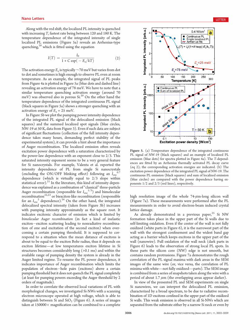
Along with the red shift, the localized PL intensity is quenchedwith increasing T, fastest rate being between 120 and 180 K. Thetemperature dependence of the integrated intensity of singlelocalized PL emissions (Figure 5a) reveals an Arrhenius-typequenching,20 which is fitted using the equation
IðTÞ ¼ I01 + C expð � Ea=kTÞ ð2Þ
The activation energy Ea is typically∼70meV but varies from dotto dot and sometimes is high enough to observe PL even at roomtemperature. As an example, the integrated signal of PL peaksfrom Figure 4a is plotted in Figure 5a (blue dots and dashed line)revealing an activation energy of 78 meV. We have to note that asimilar temperature quenching activation energy (around 70meV) was observed also in porous Si.20 On the other hand thetemperature dependence of the integrated continuous PL signal(black squares in Figure 5a) shows a stronger quenching with anactivation energy of Ea = 25 meV.
In Figure 5b we plot the pumping power intensity dependenceof the integrated PL signal of the delocalized emission (blacksquares) and the summed localized spot signals (blue circles,NW-19 at 50 K, data from Figure 3). Even if such data are subjectof significant fluctuations (collection of the full intensity depen-dence takes many hours, demanding perfect stability of theexperimental system), it can provide a hint about the importanceof Auger recombination. The localized emission often revealsexcitation power dependence with a saturation characterized bythe power-law dependence with an exponent close to 2/3. Thissaturated intensity exponent seems to be a very general featurefor Si nanocrystals. For example, Valenta et al. reported theintensity dependence of PL from single Si nanocrystals(excluding the ON/OFF blinking effect) following an Iexc
0.7
dependence (which is virtually equal to 2/3 slope withinstatistical error).21 In the literature, this kind of intensity depen-dence was explained as a combination of “classical” three-particleAuger recombination (responsible for Iexc
1/3) and bimolecularrecombination22,23 or biexciton-like recombination (responsiblefor an Iexc
2 dependence).24 On the other hand, the integrateddelocalized spectral intensity (taken from Figure 3b) increaseswith pumping intensity approximately as the square root. Itindicates excitonic character of emission which is limited bybimolecular Auger recombination (in fact a kind of inelasticexciton�exciton scattering leading to nonradiative recombina-tion of one and excitation of the second exciton) when over-coming a certain pumping threshold. It is supposed to cor-respond to a situation when the mean distance of excitons isabout to be equal to the exciton Bohr radius, thus it depends onexciton lifetime—at low temperatures exciton lifetime in Sistructures becomes considerably long (>0.1 ms) and within theavailable range of pumping density the system is already in theAuger limited regime. To resume the PL power dependence, itindicates importance of Auger recombination which limits thepopulation of electron�hole pairs (excitons) above a certainpumping threshold but it does not quench the PL signal completely(at least for pumping powers exceeding the Auger threshold by 2orders of magnitude).
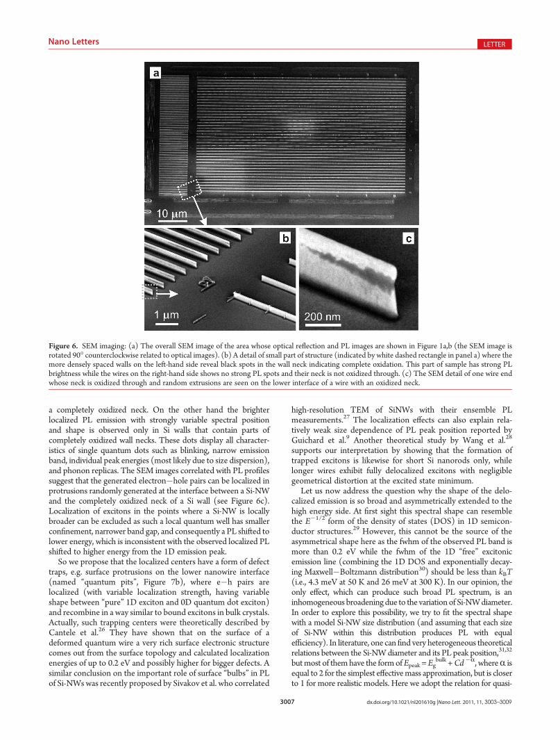
In order to correlate the observed local variations of PL withmorphological changes, we investigated Si-NWs with a scanningelectron microscope operated at high voltage, which is able todistinguish between Si and SiO2 (Figure 6). A series of imagestaken at 150000�magnification can be combined to a complete
high resolution image of the whole 74-μm-long silicon wall(Figure 7a). These measurements were performed after the PLmeasurements in order to avoid electron-beam induced crystallattice damage.
As already demonstrated in a previous paper,25 Si NWformation takes place in the upper part of the Si walls due toself-limiting oxidation. Even if the center of the wall is not fullyoxidized (white parts in Figure 6), it is the narrowest part of thewall with the strongest confinement and the widest band gapacting as a barrier which keeps excitons in the upper part of thewall (nanowire). Full oxidation of the wall neck (dark parts inFigure 6) leads to the observation of strong local PL spots. Inthese parts the silicon core (NW) edge is not smooth, butcontains random protrusions. Figure 7a demonstrates the roughcorrelation of the PL signal maxima with dark areas in the SEMimages of the same wire (or, vice versa, the correlation of PLminima with white—not fully oxidized—parts). The SEM imageis combined from a series of snapshots taken along the wire with aperiod of about 1.7 μm (the overlapping areas appear darker).
In view of the presented PL and SEM experiments on singleSi nanowires, we can interpret the delocalized PL emission,characterized by a broad spectrum, to be due to radiative recom-bination of 1D excitons confined in the upper part of the oxidizedSi walls. This weak emission is observed in all Si-NWs which areseparated from the substrate either by a narrow Si neck or even by
Figure 5. (a) Temperature dependence of the integrated continuousPL signal of NW-19 (black squares) and an example of localized PLemission (blue dots) for spectra plotted in Figure 4a). The T-depend-ences are fitted by an Arrhenius thermally activated PL decay curve(eq 2); the corresponding activation energies are indicated. (b) Theexcitation power dependence of the integrated PL signal of NW-19. Thecontinuous PL emission (black squares) and sum of localized emission(blue circles) are compared with the power dependence having ex-ponents 1/2 and 2/3 (red lines), respectively.
3007 dx.doi.org/10.1021/nl201610g |Nano Lett. 2011, 11, 3003–3009
Nano Letters LETTER
a completely oxidized neck. On the other hand the brighterlocalized PL emission with strongly variable spectral positionand shape is observed only in Si walls that contain parts ofcompletely oxidized wall necks. These dots display all character-istics of single quantum dots such as blinking, narrow emissionband, individual peak energies (most likely due to size dispersion),and phonon replicas. The SEM images correlated with PL profilessuggest that the generated electron�hole pairs can be localized inprotrusions randomly generated at the interface between a Si-NWand the completely oxidized neck of a Si wall (see Figure 6c).Localization of excitons in the points where a Si-NW is locallybroader can be excluded as such a local quantum well has smallerconfinement, narrower band gap, and consequently a PL shifted tolower energy, which is inconsistent with the observed localized PLshifted to higher energy from the 1D emission peak.
So we propose that the localized centers have a form of defecttraps, e.g. surface protrusions on the lower nanowire interface(named “quantum pits”, Figure 7b), where e�h pairs arelocalized (with variable localization strength, having variableshape between “pure” 1D exciton and 0D quantum dot exciton)and recombine in a way similar to bound excitons in bulk crystals.Actually, such trapping centers were theoretically described byCantele et al.26 They have shown that on the surface of adeformed quantum wire a very rich surface electronic structurecomes out from the surface topology and calculated localizationenergies of up to 0.2 eV and possibly higher for bigger defects. Asimilar conclusion on the important role of surface “bulbs” in PLof Si-NWswas recently proposed by Sivakov et al. who correlated
high-resolution TEM of SiNWs with their ensemble PLmeasurements.27 The localization effects can also explain rela-tively weak size dependence of PL peak position reported byGuichard et al.9 Another theoretical study by Wang et al.28
supports our interpretation by showing that the formation oftrapped excitons is likewise for short Si nanorods only, whilelonger wires exhibit fully delocalized excitons with negligiblegeometrical distortion at the excited state minimum.
Let us now address the question why the shape of the delo-calized emission is so broad and asymmetrically extended to thehigh energy side. At first sight this spectral shape can resemblethe E�1/2 form of the density of states (DOS) in 1D semicon-ductor structures.29 However, this cannot be the source of theasymmetrical shape here as the fwhm of the observed PL band ismore than 0.2 eV while the fwhm of the 1D “free” excitonicemission line (combining the 1D DOS and exponentially decay-ing Maxwell�Boltzmann distribution30) should be less than kBT(i.e., 4.3 meV at 50 K and 26 meV at 300 K). In our opinion, theonly effect, which can produce such broad PL spectrum, is aninhomogeneous broadening due to the variationof Si-NWdiameter.In order to explore this possibility, we try to fit the spectral shapewith a model Si-NW size distribution (and assuming that each sizeof Si-NW within this distribution produces PL with equalefficiency). In literature, one can find very heterogeneous theoreticalrelations between the Si-NWdiameter and its PL peak position,31,32
butmost of themhave the formofEpeak =Egbulk +Cd�R, whereR is
equal to 2 for the simplest effectivemass approximation, but is closerto 1 for more realistic models. Here we adopt the relation for quasi-
Figure 6. SEM imaging: (a) The overall SEM image of the area whose optical reflection and PL images are shown in Figure 1a,b (the SEM image isrotated 90� counterclockwise related to optical images). (b) A detail of small part of structure (indicated by white dashed rectangle in panel a) where themore densely spaced walls on the left-hand side reveal black spots in the wall neck indicating complete oxidation. This part of sample has strong PLbrightness while the wires on the right-hand side shows no strong PL spots and their neck is not oxidized through. (c) The SEM detail of one wire endwhose neck is oxidized through and random extrusions are seen on the lower interface of a wire with an oxidized neck.
3008 dx.doi.org/10.1021/nl201610g |Nano Lett. 2011, 11, 3003–3009
Nano Letters LETTER
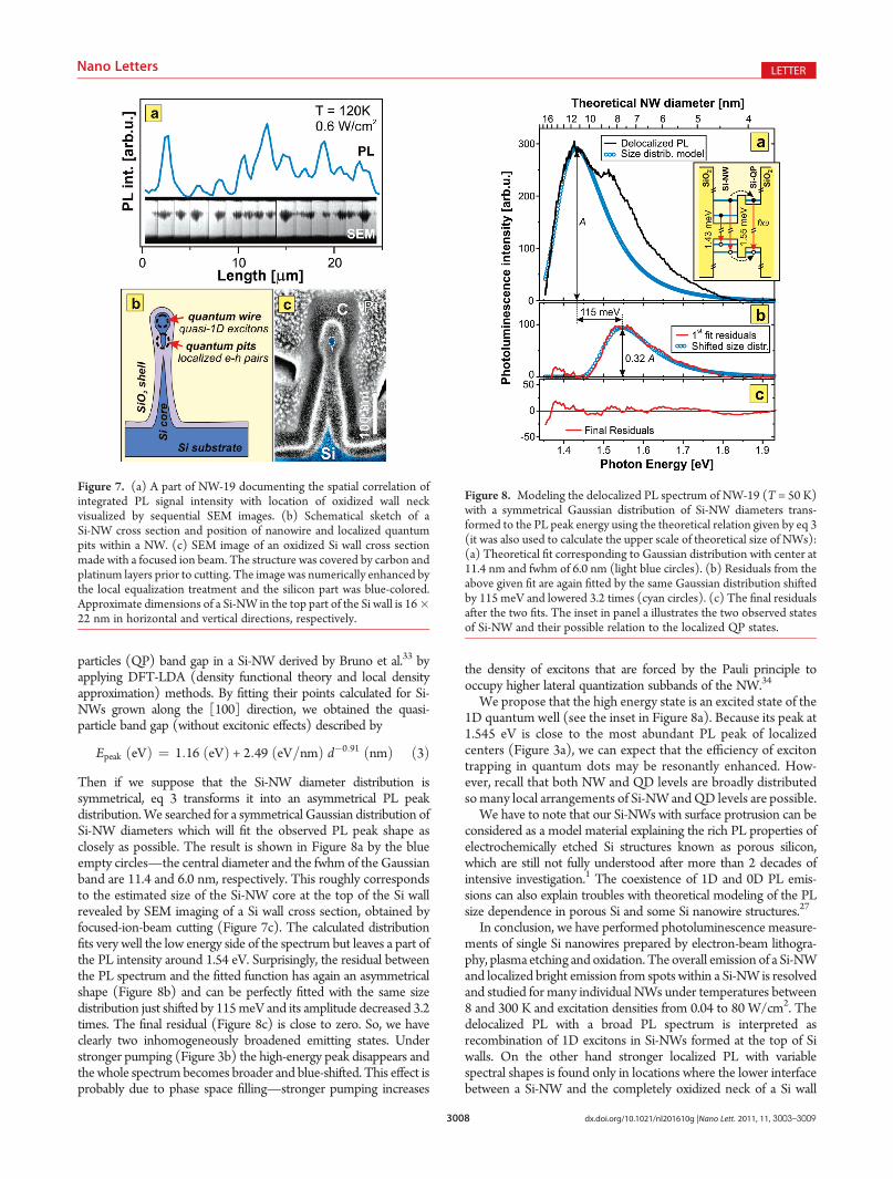
particles (QP) band gap in a Si-NW derived by Bruno et al.33 byapplying DFT-LDA (density functional theory and local densityapproximation) methods. By fitting their points calculated for Si-NWs grown along the [100] direction, we obtained the quasi-particle band gap (without excitonic effects) described by
Epeak ðeVÞ ¼ 1:16 ðeVÞ + 2:49 ðeV=nmÞ d�0:91 ðnmÞ ð3ÞThen if we suppose that the Si-NW diameter distribution issymmetrical, eq 3 transforms it into an asymmetrical PL peakdistribution.We searched for a symmetrical Gaussian distribution ofSi-NW diameters which will fit the observed PL peak shape asclosely as possible. The result is shown in Figure 8a by the blueempty circles—the central diameter and the fwhm of the Gaussianband are 11.4 and 6.0 nm, respectively. This roughly correspondsto the estimated size of the Si-NW core at the top of the Si wallrevealed by SEM imaging of a Si wall cross section, obtained byfocused-ion-beam cutting (Figure 7c). The calculated distributionfits very well the low energy side of the spectrum but leaves a part ofthe PL intensity around 1.54 eV. Surprisingly, the residual betweenthe PL spectrum and the fitted function has again an asymmetricalshape (Figure 8b) and can be perfectly fitted with the same sizedistribution just shifted by 115meV and its amplitude decreased 3.2times. The final residual (Figure 8c) is close to zero. So, we haveclearly two inhomogeneously broadened emitting states. Understronger pumping (Figure 3b) the high-energy peak disappears andthewhole spectrum becomes broader and blue-shifted. This effect isprobably due to phase space filling—stronger pumping increases
the density of excitons that are forced by the Pauli principle tooccupy higher lateral quantization subbands of the NW.34
We propose that the high energy state is an excited state of the1D quantum well (see the inset in Figure 8a). Because its peak at1.545 eV is close to the most abundant PL peak of localizedcenters (Figure 3a), we can expect that the efficiency of excitontrapping in quantum dots may be resonantly enhanced. How-ever, recall that both NW and QD levels are broadly distributedsomany local arrangements of Si-NW andQD levels are possible.
We have to note that our Si-NWs with surface protrusion can beconsidered as a model material explaining the rich PL properties ofelectrochemically etched Si structures known as porous silicon,which are still not fully understood after more than 2 decades ofintensive investigation.1 The coexistence of 1D and 0D PL emis-sions can also explain troubles with theoretical modeling of the PLsize dependence in porous Si and some Si nanowire structures.27
In conclusion, we have performed photoluminescence measure-ments of single Si nanowires prepared by electron-beam lithogra-phy, plasma etching and oxidation. The overall emission of a Si-NWand localized bright emission from spots within a Si-NW is resolvedand studied for many individual NWs under temperatures between8 and 300 K and excitation densities from 0.04 to 80 W/cm2. Thedelocalized PL with a broad PL spectrum is interpreted asrecombination of 1D excitons in Si-NWs formed at the top of Siwalls. On the other hand stronger localized PL with variablespectral shapes is found only in locations where the lower interfacebetween a Si-NW and the completely oxidized neck of a Si wall
Figure 7. (a) A part of NW-19 documenting the spatial correlation ofintegrated PL signal intensity with location of oxidized wall neckvisualized by sequential SEM images. (b) Schematical sketch of aSi-NW cross section and position of nanowire and localized quantumpits within a NW. (c) SEM image of an oxidized Si wall cross sectionmade with a focused ion beam. The structure was covered by carbon andplatinum layers prior to cutting. The image was numerically enhanced bythe local equalization treatment and the silicon part was blue-colored.Approximate dimensions of a Si-NW in the top part of the Si wall is 16�22 nm in horizontal and vertical directions, respectively.
Figure 8. Modeling the delocalized PL spectrum of NW-19 (T = 50 K)with a symmetrical Gaussian distribution of Si-NW diameters trans-formed to the PL peak energy using the theoretical relation given by eq 3(it was also used to calculate the upper scale of theoretical size of NWs):(a) Theoretical fit corresponding to Gaussian distribution with center at11.4 nm and fwhm of 6.0 nm (light blue circles). (b) Residuals from theabove given fit are again fitted by the same Gaussian distribution shiftedby 115 meV and lowered 3.2 times (cyan circles). (c) The final residualsafter the two fits. The inset in panel a illustrates the two observed statesof Si-NW and their possible relation to the localized QP states.

3009 dx.doi.org/10.1021/nl201610g |Nano Lett. 2011, 11, 3003–3009
Nano Letters LETTER
contains irregular extrusions, which most probably act as traps(quantum pits) where electron�hole pairs are localized andproduces emission similar to quasi-0D quantum dots. Our inter-pretation of luminescence properties of individual Si-NWs may beapplied to understand the extremely variable optical properties ofporous Si and other Si nanostructures. The practical consequencesof coexistence of 1D and 0D effects in Si-NWs can be multiple: (i)an optimization of the density and shapes of localized centersshould significantly increase the brightness (and reduce saturationeffects) of Si-NW PL, especially at room temperature; (ii) after amore detailed understanding of the relation between the localstructure and PL spectra, the micro-PL spectral imaging may beapplied to detailed characterization of fabricated Si-NWs; (iii) thecoexistence of delocalized and localized centers is also crucial forapplication of Si-NW as sensors and detectors.
’AUTHOR INFORMATION
Corresponding Author*E-mail: [email protected].
’ACKNOWLEDGMENT
The authors thank Professor I. Pelant and Professor S. Ossicinifor discussions. Financial support from the Swedish ResearchCouncil (VR) through an individual and a Linn�e grant is grate-fully acknowledged. Part of this work (J.V.) was supportedthrough the research centre LC510 and the research planMSM0021620835 of MSMT and the project KAN400100701of the GAAV.
’REFERENCES
(1) Silicon nanocrystals: Fundamentals, Synthesis and Applications;Pavesi, L., Turan, R., Eds.; Wiley-VCh: Weinheim, 2010.(2) Schmidt, V.; Wittemann, J. V.; G€osele, U. Chem. Rev. 2010, 110,
361–388.(3) Bandaru, P. R.; Pichanusakorn, P. Semicond. Sci. Technol. 2010,
25, 024003.(4) Kelzenberg, M. D.; Turner-Evans, D. B.; Kayes, B. M.; Filler,
M. A.; Putnam, M. C.; Lewis, N. S.; Atwater, H. A. Nano Lett. 2008, 8,710–714.(5) Sivakov, V.; Andra, G.; Gawlik, A.; Berger, A.; Plentz, J.; Falk, F.;
Christiansen, S. H. Nano Lett. 2009, 9, 1549–1554.(6) Kelzenberg, M. D.; Boettcher, S. W.; Petykiewicz, J. A.; Turner-
Evans, D. B.; Putnam, M. C.; Warren, E. L.; Spurgeon, J. M.; Briggs,R. M.; Lewis, N. S.; Atwater, H. A. Nat. Mater. 2010, 9, 239–244.(7) Agarwal, A.; Buddharaju, K.; Lao, I. K.; Singh, N.; Balasubramanian,
N.; Kwong, D. L. Sens. Actuators, A 2008, 145, 207–213.(8) Chan, C. K.; Peng, H.; Liu, G.; McIlwrath, K.; Zhang, X. F.;
Huggins, R. A.; Cui, Y. Nat. Nanotechnol. 2008, 3, 31–35.(9) Guichard, A. R.; Barsic, D. N.; Sharma, S.; Kamins, T. I.;
Brongersma, M. L. Nano Lett. 2006, 6, 2140–2144.(10) Walavalkar, S. S.; Hofmann, C. E.; Homyk, A. P.; Henry, M. D.;
Atwater, H. A.; Scherer, A. Nano Lett. 2010, 10, 4423–4428.(11) Qi, J.; Belcher, A. M.; White, J. M. Appl. Phys. Lett. 2003,
82, 2616–2618.(12) Dovrat, M.; Arad, N.; Zhang, X. H.; Lee, S. T.; Sa’ar, A. Phys.
Status Solidi A 2007, 204, 1512–1517.(13) Guichard, A. R.; Kekatpure, R. D.; Brongersma, M. L. Phys. Rev.
B 2006, 78, 235422.(14) Ma, D. D. D.; Lee, S. T.; Shinar, J. Appl. Phys. Lett. 2005,
87, 033107.(15) Liu, H. I.; Biegelsen, D. K.; Ponce, F. A.; Johnson, N. M.; Pease,
R. F. W. Appl. Phys. Lett. 1993, 64, 1383–1385.
(16) Bruhn, B.; Sangghaleh, F.; Linnros, J. Phys. Status Solidi A 2011,208, 631–634.
(17) Valenta, J.; Bruhn, B.; Linnros, J. Phys. Status Solidi C 2011, 8,1017–1020.
(18) Sychugov, I.; Juhasz, R.; Valenta, J.; Linnros, J. Phys. Rev. Lett.2005, 94, 087405.
(19) Sze, S. M. Physics of Semiconductor Devices, 2nd ed., WileyInterScience, New York, 1981.
(20) Andersen, O. K.; Veje, E. Phys. Rev. B 1996, 53, 15643–15652.(21) Valenta, J.; Fucikova, A.; Vacha, F.; Adamec, F.; Humpol�i�ckov�a,
J.; Hof, M.; Pelant, I.; K�usov�a, K.; Dohnalov�a, K.; Linnros, J. Adv. Funct.Mater. 2008, 18, 2666–2672.
(22) M’gha€ieth, R.; Maaref, H.; Mihalcescu, I.; Vial, J. C. Phys. Rev. B1999, 60, 4450–4453.
(23) Tayagaki, T.; Fukatsu, S.; Kanemitsu, Y. Phys. Rev. B 2009, 79,041301.
(24) Dal Negro, L. PhD thesis, Universit�a di Trento, 2003.(25) Bruhn, B.; Valenta, J.; Linnros, J. Nanotechnology 2009, 20,
505301.(26) Cantele, G.; Ninno, D.; Iadonisi, G. Phys. Rev. B 2002, 61,
13730–13736.(27) Sivakov, V. A.; Voigt, F.; Berger, A.; Bauer, G.; Christiansen,
S. H. Phys. Rev. B 2010, 82, 125446.(28) Wang, Y.; Zhang, R.; Frauenheim, T.; Niehaus, T. A. J. Phys.
Chem. C 2009, 119, 12935.(29) Dawies, J. H. The physics of low-dimensional semiconductors: An
introduction; Cambridge University Press: Cambridge and New York,1998.
(30) Peyghambarian, N.; Koch, S. W.;Mysyrowicz, A. Introduction toSemiconductor Optics; Prentice Hall: Englewood Cliffs, NJ, 1993.
(31) Li, J.; Freeman, A. J. Phys. Rev. B 2006, 74, 075333.(32) Yao, D.; Zhang, G.; Li, B. Nano Lett. 2008, 8, 4557–4561.(33) Bruno, M.; Palummo, M.; Marini, A.; Del Sole, R.; Ossicini, S.
Phys. Rev. Lett. 2007, 98, 036807.(34) Forchel, A.; Kieseling, F.; Braun, W.; Ils, P.; Wang, K. H. Phys.
Status Solidi B 1995, 188, 229–240.