codecs: a mixed-level circuit and device simulator
TRANSCRIPT
CODECS: A Mixed-Level Circuit and Device Simula
by
Kartikeya Mayaram
Memorandum No. UCB/ERL M88/71
November 1988
CODECS: A Mixed-Level Circuit and Device Simulator
bY
Kartikeya hfayaram
Abstract
CODECS is a mixed-level circuit and device simulator that provides a dm
between technology parameters and circuit performance. Detailed and accurate a
of semiconductor circuits are possible by use of physical (numerical) models for
devices. The numerical models are based upon solution of Poisson’s equation a
current-continuity equations. Analytical models can be used for the noncritical del
The goal of this research has been to develop a general framework for mixe
circuit and device simulation that supports a wide variety of analyses capabiliti
numerical models. Emphasis has been on algorithms to couple the device simulatc
the circuit simulator and an evaluation of the convergence properties of the c
simulator. Different algorithms have been implemented and evaluated in CODECS
Another aspect of this research has been to investigate critical applicati
mixed-level circuit and device simulation. Typical examples include simulation o
level injection effects in BiCMOS driver circuits, non-quasi-static MOS op
switch-induced error in MOS switchedcapacitor circuits, and inductive turn off
rectitlers. For these examples conventional circuit simulation with analytical
gives inaccurate results.
CODECS incorporates SPICE3 for the circuit-simulation capability and for i
cal models. A new one- and two-dimensional device simulator has been dev
CODECS supports dc, transient, small-signal ac, and pole-zero analyses of
1
t link
ilyses
itical
d the
ces.
-level
; and
with
upled
1s of
high-
ation,
if pin
,odels
ialyti-
oped.
rcuits
2
containing one- and two-dimensional numerical models for diodes and bipolar
and two-dimensional numerical models for MOSFETs.
CODECS include physical effects such as bandgap narrowing,
Auger recombinations, concentration and fielddependent
dependent lifetimes, and avalanche generation.
Donald 0. Pederson
Committee Chairman ~

Acknowledgements
This research has been made possible by a grant from the Semicanductor R
Corporation. 1 am pleased to acknowledge their financial support.
I thank Professor Donald Pederson, my research advisor, for having given
opportunity to work on interesting projects during my graduate studies at Berke
has been an excellent mentor and I am grateful to him for his advice and guida
matters both technical and nontechnical. His continuous support and enmurageme
cheered me up when I was in low spirits and inspired me to perform my best. Frc
I have also learned presentation skills, writing skills, and teaching skills.
Professor Chewing Hu’s courses on semiconductor device physics gavc
strong foundation in device physics. He has provided me with excellent guidance
the course of my studies and I thank him for his support
I have also received valuable guidance from Professor Robert Dutton of S
University. He gave me a special treatment (his students tell me that I saw more
than they did) and made significant suggestions on critical applications of CODEC
Professors Paul Gray, David Hodges, Ping KO, Richard Newton, and
Sangiovanni-Vincentelli also gave me valuable advice. I take this opportunity tl
them for teaching state-of-the-art courses and for broadening my horizons.
Dr. Roberto Guemeri of University of B o l o p , Italy, provided insight in
simulation and my discussions with him were extremely helpful.
I am grateful to Dr. James Dyer, now at Polaroid Corporation, for his help
encouraging me to pursue graduate studies at UC Berkeley. I thank Dr. ’
McCalla of Hewlett Packard and Dr. Andrei Vladimirescu of Analog Design TI
their continued interest and support, and Mr. Ted Vucurevich of Analog Dev
earch
le the
y. He
.e, on
have
lhim
me a
nford
fhim
lberto
thank
levice
id for
illiam
11s for
:s for

supporting the Lispbased simulation work. The loan of a Symbolics Lisp machin from
Analog Devices and Symbolics Inc. is gratefully acknowledged. 1
Laboratories. ~
I
During the c o m e of my research work I have benefited from discussions wi
Herman Gummel, Peter Llyod, Jim Prendergast, and ashore Singhal of AT&
Drs.
Bell
I have been privileged to work with many talented students during my stay at
Berkeley. Jeff Burns and Jack Lee gave me critical advice and support during qficult
times. Conversations with The0 Kelessoglou were most beneficial. Cormac Conriy and
David Gates gave valuable comments on initial drafts of the thesis. Tom Quarlds was
most helpful with SPICE3. Without his help CODECS could not be in its present/ form.
Discussions with Ken Kundert were also beneficial. Geert Rosseel of Stanford dniver-
I
s i 9 was the first outside user of CODECS. I thank him for his patience in using
CODECS and for applications of CODECS to BiCMOS drivers. My silent th s to
Most of all, I thank my parents, sisters, and my wife, Namita, for their c L nstant
others whose names I cannot mention because of space constraints.
love and support and for their patience during the c o m e of this work. I am grattful to
Namita for keeping me in good cheer and for all the sacrifices that she has made f4r me.
TABLE OF CONTENTS
CHAPTER 1 Introduction ..................................................................................
CHAPTER 2 An Overview of Circuit Simulation and Modeling ...................
2.1 Introduction ...............................................................................................
2.2 The Circuit-Simulation Problem ................................................................
2.2.1 Dc and Transient Analyses ...............................................................
2.2.2 Small-Signal ac Analysis ..................................................................
2.2.3 Pole-Zero Analysis ...........................................................................
Semiconductor Device Modeling for Circuit Simulation .......................... 2.3
2.3.1 A ~ l y t i c a l Models .............................................................................
2.3.2 Table Models ....................................................................................
2.3.3 Quasi-Numerical Models ..................................................................
2.3.4 Numerical Models .............................................................................
CHAPTER 3 An Overview of Device Sirnulation .............................................
3.1 Introduction ...............................................................................................
3.2 The Device-Simulation Problem ................................................................
3.3 Physical Models for Device Simulation ...................................................
3.3.1 Carrier-Mobility Models ...................................................................
3.3.2 Carrier Generation and Recombination Models ................................
i
1
1
1
8
9
15
16
17
17
24
26
27
29
29
30
32
32
35
3.3.3 Heavy-Doping Effects ......................................................................
3.4 Boundary Conditions .................................................................................
3.5 Choice of Independent Variables ...............................................................
3.6 Scaling of Semiconductor Equations ......................................................... 3.7 Space-Discretization Techniques ...............................................................
3.7.1 Finite-Difference Discretization ........................................................
3.7.2 The Finite-Element Method ..............................................................
3.7.3 GridIMesh Generation ......................................................................
3.8 Solution Methods for Device Equations ....................................................
3.8.1 Dc and Transient Analyses ...............................................................
3.8.2 Small-Signal ac Analysis ..................................................................
CHAPTER 4 Coupled Device and Circuit Simulation .....................................
4.1 Introduction ...............................................................................................
4.2 Dc and Transient Analyses ........................................................................
4.2.1 The Two-Level Newton Algorithm ..................................................
4.2.2 Calculation of Conductances ............................................................
4.2.3 Architecture of CODECS .................................................................
4.2.4 The Full-Newton Algorithm .............................................................
4.2.5 Implementation Issues .......................................................................
4.2.6 Convergence Properties for dc Analysis ...........................................
4.2.7 Transient Analysis Comparisons .......................................................
ii
36
38
41
43
44
45
48
50
51
52
54
57
57
59
59
62
65
66
69
72
74
4.2.8 Conclusions on Performance. Convergence. and Memory Re-
quirements ...................................................................................................
4.2.9 Parallelization Issues .........................................................................
4.3 Small-Signal ac Analysis ...........................................................................
4.3.1 Calculation of ac Admittances ..........................................................
4.4 Pole-Zero Analysis ....................................................................................
4.5 Requirements on Circuit and Device Simulators .......................................
CHAPTER 5 Device-Level Algorithms of CODECS ........................................
5.1 Introduction ...............................................................................................
5.2 Space Discretization in Two Dimensions ..................................................
5.3 Space Discretization in One Dimension ....................................................
5.3.1 Base Boundary Condition for One-Dimensional Bipolar Transis-
tor ................................................................................................................
5.4 Dc Analysis ...............................................................................................
5.4.1 Device-Based Limiting Scheme ........................................................
5.4.2 Voltage-Step Backtracking ...............................................................
5.4.3 Linear Prediction of Initial Guess .....................................................
5.4.4 Norm-Reducing Newton's Method ...................................................
5.5 Transient Analysis .....................................................................................
5.5.1 Local EHO~ and Error Estimates .......................................................
5.5.2 Estimation of Local Emor .................................................................
iii
77
78
79
80
80
81
83
83
84
91
91
95
95
97
98
101
103
105
108
5.5.3 Time-Step Control in CODECS .......................................................
5.5.4 Higher-Order Integration Methods ....................................................
5.5.5 Time-Step and Order Control for Higher-Order BDF ......................
5.5.6 Iteration-Domain Latency .................................................................
5.5.7 Current-Conservation Property of BDF ............................................
5.6 Small-Signal ac and Pole-Zero Analyses ..................................................
5.7 Calculation of Sensitivity to Doping Profiles ............................................
5.7.1 Implementation of Sensitivity Calculations ......................................
7.5 Runtime Comparisons with Analytical Models .........................................
5.7.2 Sensitivity Simulation Examples ......................................................
CHAPTER 6 CODECS Design Considerations ................................................
6.1 Introduction ...............................................................................................
207
6.2 LispBased Implementation . CODECSlisp ..............................................
6.2.1 Runtime Performance .......................................................................
6.3 C-Based Implementation of CODECS ......................................................
Runtime Performance and Comparisons to CODECSlisp ................ 6.3.1
CHAPTER 7 Comparison of Analytical and Numerical Models ....................
iv
111
119
123
124
130
131
136
139
140
147
147
148
148
154
155
159
CHAPTER 8 Applications of CODECS ............................................................
8.1 introduction ...............................................................................................
8.2 Analysis of BiCMOS Driver Circuits .......................................................
8.2.1 Delay Analysis ..................................................................................
8.2.2 Technology and Supply-Voltage Scaling Effects .............................
8.3 P-i-o Diode Turn Off ................................................................................
8.3.1 Reverse Recovery of pi-n Diodes ....................................................
8.3.2 Operation Under Breakdown Conditions ..........................................
8.3.3 Snubber Circuit Design .....................................................................
8.4 Evaluation of Switch-Induced Errors ........................................................
8.5 Evaluation of Analytical Models ...............................................................
CHAPTER 9 Conclusions ...................................................................................
APPENDIX A CODECS User’s Guide .............................................................
APPENDIX B CODECS Benchmark Circuits ..................................................
APPENDIX C Source Listing of CODECS .......................................................
REFERENCES ......................................................................................................
V
211
211
212
214
220
225
227
242
252
254
262
267
273
297
306
307
CHAPTER 1
Introduction
Simulation plays an important role in the design of present day integrated
(ICs), devices, and processes. Alternative design techniques can be quickly evalua
various ~~adeoffs can be determined before a circuit or device is fabricated.
cation of circuits and devices is time consuming and costly, simulation provi
efficient and attractive way to explore the design space [1.1].
Various types of simulations currently in use, from the process level to the
level, are depicted in Figure 1.1. Also shown is the relationship between
simulation. Two branches are shown, one the experimental branch
computational or simulation branch. Corresponding to each step in
branch there is a simulation step that serves a similar purpose. The
produce circuits that are functionally correct and meet the desired
achieved in an iterative manner until the design converges to the
tions may not completely eliminate repeated fabrications but they
number of iterations that are required. As an example, there is
savings in simulating a process step compared to laboratory costs [ 1.11.
A simulator that combines two or more levels of simulation
simdutor. The key idea behind a mixed-level simulator is to use detailed forms
lation on the critical parts of a circuit, to get precise waveform information,
accurate but faster forms of simulations for the rest of the circuit.
deoff between the accuracy of the simulations and the runtime. The
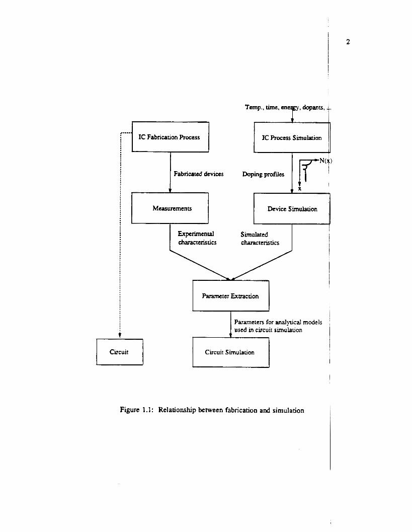
IC Fabrication Process .....
Fabricated devices
Measurements
r l clrcuit
IC proCess Simulation
iT"( Doping profiles
Device Simulation
~~
Experimental Charaneristics
Simulated characteristics
Parameters for analytical models used in circuit simulation 1 r - l Circuit Simulation
Figure 1 . 1 : Relationship between fabrication and simulation
2
and device simulator CODECS is described in this dissertation. Some critical a]
tions of mixed-level circuit and device simulation are also pnscnted.
Early work in mixed-level simulation was devoted to combining circuit, timi1
logic-level simulations SPLICE1 [1.2], DIANA [1.3]. In later work mixed-level s
tion was used to combine circuit and logic simulations in SAMSON [1.4], and (
logic and register-transfer-level simulations in SPLICE2 [ 1.51.
0
In general, mixed-level simulation has been used extensively to combine the
level of simulation with higher levels of simulation. Another direction in which 1
level simulation can be used is to combine circuit simulation with device simulai
has been done in MEDUSA El.61 and SIFCOD [1.7]. This approach has several
tages. Devices can be simulated under realistic dc and time-dependent boundary
tions imposed by the circuit in which they are embedded. Conventional devicl
simulation typically allows only voltage or current boundary conditions for a c
and, hence, cannot account for circuit embedding. Furthermore, with a mixed-lev
cuit and device simulator one can simulate circuits even in the absence of ana
models* for semiconductor devices. If the doping profiles and the geometry of th
ice are available, then circuits can be simulated. This provides a predictive capab
the circuit level, since the impact of process changes and alternate device designs (
cuit performance can be determined. Such a simulator provides a direct link be
technology and circuit performance. In addition, developers of analytical mode
semiconductor devices can use the mixed-level circuit and device simulator as a
for verifying the models for the circuit simulator. Physical effects, that are importa
must be incorporated, can be determined and their effect on circuit performance t
evaluated.
* Analytical models refer to mathematical expressions that relate the terminal currents to the termina tages of a device.
3
plica-
5 and
nula-
rcuit,
ircuit
Jxed-
on as
5 V a n -
ondi-
-level
:vice;
1 cir-
ytical
dev-
ity at
n cir-
ween
s for
leans
t and
m b e
vol-

4
models. A coupled device and circuit simulator, called CODECS, is the result
research. The simulation environment of CODECS enables one to model critical
within a circuit by physical (numerical) models based upon the solution of
equation and the current-continuity equations. Analytical models can be used
noncritical devices. CODECS supports dc, transient, small-signal ac, and pole/zercl
lyses of circuits containing one- and two-dimensional numerical models for diodes
of this
d.:vices
Poi5son’s
for the
ana-
and
bipolar transistors, and two-dimensional numerical models for MOSFETs. In additi
and transient sensitivities to doping profiles can be computed at the device level
numerical models in CODECS include physical effects such as bandgap narra
Shockley-Hall-Read and Auger recombinations, concentration and fielddependent I
ities, concentrationdependent lifetimes and avalanche generation.
An effective coupling of the device and circuit-simulation capabilities is acl
by a proper choice of algorithms and architecture. Various algorithms to coup
device-level and circuit-level simulators have been implemented in CODECS.
algorithms are evaluated based on the convergence properties and runtime perfon
of the coupled simulator. This study also provides guidelines for choice of a pan
algorithm.
Another aspect of this research has been to investigate critical applicatia
mixed-level circuit and device simulation. Typical examples include simulation of
level injection effects in BiCMOS buffer circuits, non-quasi-static MOS ope1
switch-induced error in MOS switched-capacitor circuits, and inductive turn off
rectifiers. For these examples conventional circuit simulation with analytical n
gives inaccurate results.
This report is organized in the following manner. Chapter 2 provides an ove
of circuit simulation and the various techniques used for modeling of semiconducto
ices for use in circuit simulators. In Chapter 3 an overview of the physical models
at the device level of simulation is provided. This is followed by a description
space-discretization techniques and the solution algorithms. The problem of mixed
circuit and device simulation is addressed in Chapter 4. A Framework is proposed f
mixed-level simulator and algorithms to couple the device and circuit simulatoi
described. The convergence properties of the coupled simulator are also investi
Chapter 5 describes in detail the algorithms used in CODECS and the techniques
5
a dc
The
vhg,
obil-
eved
: the
hese
ance
cular
IS of
iigh-
ition,
f pin
Idels
view
dev-
used
f the
level
r the
i are
ated.
used
for enhancing dc convergence. An initial prototype of CODECS was developed in
and Chapter 6 provides a speed performance comparison of the LISP-based versioi
the new version in the C language. A comparison of the tradeoffs involved in 1
analytical models is described in Chapter 7 and several applications of CODEC
illustrated in Chapter 8. Finally, the major contributions of this research are summ
in Chapter 9 and possible directions for future research are also listed.
6
LISP
with
se of
Sare
u i zed
CHAPTER 2
An Overview of Circuit Simulation and
Semiconductor Device Modeling
2.1. Introduction
Circuit-level simulation is one major component of a mixed-level circuit a n c
simulator. This chapter provides an overview of the circuit-simulation problem
the nonlinear dc and transient analyses are introduced and the solution tec
currently in use, namely, the direct and relaxation-based methods are described.
followed by a description of the small-signal ac and pole-zero analyses.
Modeling of semiconductor devices plays an important role in circuit sim
The simulation results are reliable only if accurate models are used for the
Accuracy of a model is related to the application. For some simulations, such as 1
digital circuits, precise models are not necessary. On the other hand, simulation
log and other high-performance circuits mandates the use of "exact" models. A
that is suited to the simulation of digital circuits may be inappropriate for sin
analog circuits. There is a tradeoff between the accuracy of a model and the sin
runtime. Therefore, different models are used depending on the speed and a
requirements of a simulation. Commonly used approaches to modeling of semica
devices can be classified as: analytical models, empiricalhble models, quasi-nL
models, and numerical models.
7
levice
First,
uques
'h is is
ation.
vices.
)se of
. ana-
nodel
lating
lation
uracy
iuctor
erica1
The modeling task involves use of a particular technique to model accurately
static (dc) and dynamic (transient) operation of the device. First, a model is
for the dc operation. Then, the dc model is enhanced for use in transient analysis
incorporating charge-storage effects.
Analytical models are by far the most popular and are addressed in detail
chapter. These models relate the terminal currents and voltages of a device by
form expressions. An understanding of the device physics provides a first-order
ship between the terminal currents and voltages. Second-order physical effects are
porated by empirical factors. Nonetheless, several deficiencies exist in analytical
the
de\,eloped
by
in this
closed-
relation-
incor-
nodels
2.2. The Circuit-Simulation Problem
and these are also described.
A brief description of the other modeling techniques is also provided a l o q
their advantages and limitations.
Circuit simulation consists of two distinct phases, an equation-assembly phage fol-
lowed by an equation-solution phase. Circuit-level equations can be assembled by the
with
combined use of the Kirchoff s current and voltage laws (KCL and KVL) along with the
branchconstitutive relations for each element in the circuit [2.1]. Such an approbch to
formulating the circuit equations is called the Sparse-Tableau Approach (STA) p d is
used in the simulation program ASTAP [2.2]. However, the number of eqqations
describing the circuit is large; n + 2b equations for a circuit with n + 1 nodes /md b
branches.
Nodal Analysis (NA) [2.1] requires only n equations, for a circuit with
nodes. However, NA is restrictive in that it allows only elements which are
trolled, Le., elements for which the terminal currents can be expressed .as
the terminal voltages. Modified Nodal Analysis (MNA), first used by
formalized by 12.41, accommodates nonnodul elements and for this reason is pr
and has been used in SPICE [2.3, 2.51. MNA allows all types of circuit elemei
results in a system of equations that, although larger in size compared to NA,
considerably smaller than STA.
2.2.1. Dc and Transient Analyses
Dc and transient analyses are presented in this section. The transient sim
problem is introduced and the dc operating point analysis is shown to be a speci
of the general transient problem. The dc operating point solution provides the initi
dition for transient analysis and is computed before starting the transient simulatioi
Transient simulations are by far the most frequently used analyses in circuit I
The dynamic response of a circuit is described by a system of nonlinear diffei
algebraic equations obtained from the equation-assembly phase. These equations
written in a general form as
where x is the vector of unknowns, Le., the node voltages and the currents throug
nodal elements, u is the excitation vector, z is the vector of capacitor charges and
tor fluxes, f is a nonlinear vector-valued function obtained from an MNA formula
the circuit equations, and g is a nonlinear vector-valued function that relates the I
tor charges and inductor fluxes to the capacitor voltages and inductor currents, 1
tively. The initial conditions are obtained by setting z(0) = 0 and solving the no
algebraic equations
f(0, X(O), u(0)) = 0
The solution vector ~0 = x(0) is called the dc operating point solution of the circu
9
:rred
and
Still
ition
case
con-
s i p .
dal-
n be
:2.1)
non-
due-
In of
Iaci-
Pet-
near
:2.2)
The
10 i
capacitor charges and inductor fluxes at time t = 0 are given by the algebraic
ship
lation- i For a dc operating point analysis the nonlinear Equation (2.2) is solved. ' s is
done by an iterative approach and the Newton-Fbphson method is frequently us since
it has local quadratic convergence [2.3, 2.61. Use of Newton's method results in the
solution of a linear system of equations for each iteration. This system of equa 'ons is given by I
I
J(d)Ad+' = -f(#) 1 (2.4)
where J(xk) = [ - is the Jacobian matrix of the circuit-level equations, and 4 is the
iteration number. Equation (2.4) is solved at each iteration for &+', which is sed to
calculate the new iterate, d+' = 2 + &+'. This is done until convergence is e d
( I I & + ' I I e E, where E is a user-specified error tolerance). Alternatively, guation
I
.p
(2.4) can be written as
Xk+' = Xk - [ J ( X q - ' f ( X k )
This system of equations is obtained from the companion circuit [2.7] of
under consideration. The companion circuit is a linear circuit obtained from
nonlinear circuit by replacing all nonlinear elements by their linear
[2.7]. SPICE makes use of the companion circuit and the equations
form of Equation (2.5). The linear equations are solved by
decomposition. In general, the system of circuit equations is
matrix techniques are used [2.6, 2.81.
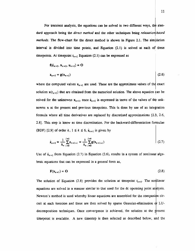
For transient analysis, the equations can be solved in two different ways, th
dard approach being the direcr merhod and the other techniques being reluxurion
merhods. The flow-chart for the direct method is shown in Figure 2.1. The sim
interval is divided into time points, and Equation (2.1) is solved at each of
timepoints. At timepoint rn+l Equation (2.1) can be expressed as
f(in+lr Xn+l, un+1) = 0
zn+1 = g(Xn+1)
where the computed values x,+~ are used. These are the approximate values of t h t
solution x(r,+,) that are obtained from the numerical solution. The above equation
solved for the unknowns x,,+~, once in+, is expressed in terms of the values of th
noms x at the present and previous timepoints. This is done by use of an intel
formula where all time derivatives are replaced by discretized approximations [2.
2.81. This step is know as time discretization. For the backward-differentiation foi
(BDF) [2.9] of order k, 1 I k 5 6 , in+, is given by
* i=k i=k
z n + 1 = - C Z n + l - i = - Cg(xn+l-i) hn i d hn i d
Use of
braic equations that can be expressed in a general form as,
from Equation (2.7) in Equation (2.6), results in a system of nonlinea
F(xn+l) = 0
The solution of Equation (2.8) provides the solution at timepoint rn+l. The no
equations are solved in a manner similar to that used for the dc operating point ar
Newton’s method is used whereby linear equations are assembled for the compani
cuit at each iteration and these are then solved by sparse Gaussian-elimination
decomposition techniques. Once convergence is achieved, the solution at the : timepoint is available. A new timestep is then selected as described below, a
11
stan-
Pased
ation
these
exact
m be
unk-
ation
2.6,
iulae
(2.7)
alge-
inear
lysis.
n cir-
LU-
esent
d the
- r
Usenewh, <
Figure 2.1 : Flowchart for transient analysis
- n = n + l Yes
<

equations are solved at the new timepoint in a similar manner. The timestep is
such that error in time discretization due to the integration formula is less than
specified error tolerance [2.3, 2.91.
The relaxation-based methods differ from the direct method in that all equal
not solved simultaneously; rather they are solved in a decoupled manner. Thus C
elimination or LU decomposition is not required, and a substantial improvement
time performance can be achieved, particularly for large circuits where a large s j
equations has to be solved. These methods work extremely well when there is I
back or strong coupling between nodes; the equations are effectively decouple
feedback some of the equations are coupled; hence, a relaxation approach may c
very slowly, if at all. Two relaxation-based methods that have been successfully 1
Iterated Timing Analysis (ITA) 12.101 and Waveform Relaxation (WR) [2.11
These methods differ in the manner in which the equations are decoupled.
In ITA, the nonlinear differential-algebraic equations are discretized in tin
the direct method. The nonlinear algebraic equations at each timepoint are then
by use of a Gauss-Seidel or a Gauss-Jacobi approach [2.10] instead of a direct s
The relaxation is at the nonlinear algebraic-equation level. For a Gauss-Jacol
rithm, the n-th equation is solved for the n-th unknown, with an estimate for thr
of all the other unknowns at the first iteration. At other iterations the values fi
previous iteration are used. This process is repeated until convergence is reachec
whole system of equations.
In general, each equation is a nonlinear equation, and the nonlinear equatio
to be solved by use of an iterative method. In ITA Newton’s method is used. H
the equations are not solved to convergence, instead only one iteration of N
method is used. It can be shown that both the Gauss-Jacobi-Newton and Gauss
Newton loops have linear convergence [2.10]. Once the solution has been obtaii
13
:lected
user-
ns are
ussian
n run-
em of
feed-
With
iverge
XI are
2.121.
as in
;olved
ution.
algo-
ralues
m the
)n the
I have
vever,
vton’s
eidel-
d at a
I 14
timepoint, the next timepoint is selected based on an errorcontrol criteria, and the
process is repeated. It can be shown that if there is a grounded capacitor at eack
ITA will converge. This assumption is quite realistic for many digital-MOS
With ITA the multirate and latency present in the circuit can also be exploited
event-driven simulation technique [2.10].
With WR the relaxation is applied at the nonlinear differential-equatior
[2.11]. The unknowns are the node-voltage waveforms. For each relaxation
new waveforms are computed for the node voltages. The differential equations
decoupled by use of a Gauss-Seidel or a Gauss-Jacobi method [2.12]. For the
Jacobi algorithm, the n-th differential equation is solved for the voltage wavefxm
node n , with an estimate for the voltage waveforms at the other nodes of the
whole
node,
circuits.
using an
level
iteration,
:an be
3auss-
at
cixuit at
tightly coupled circuits. They work well for many digital-MOS circuits where the signal
some of the nodes are strongly coupled to one another and the equations must be
simultaneously as in the direct method. Thus, another approach combines the
tages of the direct method with that of the relaxation-based approaches.
algorithms [2.12, 2.133 are used to identify the strongly coupled blocks within a
solved
advan-
Partiioning
circuit.
2.2.2. Small-Signal Ac Analysis
Small-signal ac analysis is of interest in the simulation of analog circu
involves determining the response of a circuit to a "small" sinusoidal excitation I
dc operating point has been established. The magnitude of the excitation is such tl
operation of the nonlinear circuit is linear around the operating point and no sign
harmonics are generated.
Consider the circuit equations given by Equation (2.1). Assume the dc opc
point is given by xo and Q. A small perturbation is assumed in the excitation vectr
the new excitation, represented as a phasor, is given by u = uo + i i e j W , where
complex quantity and o is the frequency of the sinusoidal sources. All input sourc
assumed to be of the same frequency. In response to this perturbation the solutio:
tor x is given by x = ~0 + Sueiw such that the circuit constraints (KCL and KVI
still satisfied. The small-signal ac response is obtained by a truncated Taylor
expansion of Equation (2.1) around the operating point; the linear terms are retainec
af -@ - uo) af . af f(i, x, u) = f(0, xo, uo) + -2 + -(x - xg) + ai ax aU
In Equation (2.9), f(0, xo, ug) is zero since ~0 is the dc operating point solutior
left-hand-side is also zero, since the perturbed response does not violate the circui
straints. Therefore, the linearized equations are given by
af ' af af aZ ax au ,g(q)joSu+ -Su + -0 = 0
From Equation (2.10) the small-signal ac solution Su is given by
15
3. It
ter a
It the
icant
ating
r and
is a
s are
vec-
1 are
eries
, and
The
con-
2.10)
2.1 1)
16
The above equations are a function of the frequency, a; hence, the
also a function of the same frequency. At a particular frequency, the
are assembled with MNA or NA as in dc or transient analyses.
are represented by linearized admittances which are used for
The complex linear system of equations is then solved by
LU-decomposition techniques. With different values of o
over a range of frequencies.
2.2.3. Pole-zero Analysis
Pole-zero analysis is useful when a designer is interested in determining thk poles
and zeros of a transfer function, i.e., the natural frequencies of the circuit +d the
transmission zeros of the transfer function. The transfer function, ~ ( s ) , of a 1 circuit
linearized at an operating point can be represented as, ! (2.12)
I
where s = CY + j w is the complex frequency. The zeros of N (s) are the zeros f T (s)
and the zeros of D (s) are the poles of T (s). Therefore, the poles and zeros of T s.) can I be obtained from the zeros of the polynomials N (s) and D (s). These polynomials are
determinants of admittance matrices; the determinant can be obtained by decodposing
the matrix in LU factors and taking the product of the diagonal terms.
,
The zeros of the polynomials are found by an iterative root-finding method
Muller’s method [2.8]. Since the number of roots are not known u priori, a tern
procedure [2.8] must also be used to terminate the root-finding algorithm. Altern
other techniques can be used [2.14].
uch as
ination
itively,

23. Semiconductor Device Modeling for Circuit Simulation
Regardless of the circuit-level analysis and the solution methods used to sc
circuit-level equations, branchconstitutive relations are required that model the se
ductor devices. Device models describe the physical operation of a device by prot
relationship between the terminal currents and the terminal voltages. Once this rl
ship is known, the companion circuit for the nonlinear semiconductor device
obtained given the terminal voltages.
Several approaches are currently in use for modeling of the semiconductor c
These can be classified under four major categories: analytical, empirical/table
numerical, and numerical. There is always a tradeoff between the accuracy obtain1
a model and the computation time required to calculate the equivalent conductanc
currents, to be used in the companion circuit, for given t e m h a l voltages. A sin
is only as good as the models used for the semiconductor devices. An inaccurate
results in erroneous simulation results. Therefore, modeling is very critical for
simulation and this section addresses the different approaches used in modeling.
approaches to modeling are described along with their advantages and disadvantag
23.1. Analytical Models
Analytical models are generally derived from an understanding of the phj
device operation under some restricted conditions such that closed-form expressic
be obtained for the terminal characteristics. Typically, a piecewise-uniform do
assumed within the device, and use is made of the drift-diffusion equations to ob
current-voltage characteristics for the semiconductor devices under dc conditions.
ical parameters are introduced to model higher-order physical effects. Some
examples of this approach are the Ebers-Moll model [2.15] for the bipolar transis
the Shichman-Hodges model (2.161 for MOSFETs. These models are often ina
17
'e the
icon-
ing a
ition-
u1 be
rices.
semi -
with
E and
ation
30dd
ircuit
rious
cs of
s can
ng is
n the
mpir-
mple
r and
quate

for modeling present day integrated devices; hence, there is a significant researc effort
for obtaining better models that account for all the important physical phenome within
the device. The Gummel-Poon model [2.15, 2.171 has been the workhorse for s' dation
of bipolar integrated circuits and has proved to be extremely useful. However, resent
day bipolar devices cannot be adequately modeled by this model and once again ere is
need for a better model to replace the Gummel-Poon model [2.18, 2.191. For M SFETs
a unified model has not emerged [2.20-2.31 J and even today new models are co stantly
being developed r2.32-2.361. ~
A model that is used for a particular device is characterized by a set of p eters
called the model parameters. These parameters are the various constants that ap ear in
the closed-form expressions relating the terminal currents to the terminal voltaged. Their
values are determined from the measured characteristics of a device. Typically, qarame-
ter extraction relies on curve fitting such that the data from the analytical model is in
I reasonable agreement with the measured data. Since the number of parameter to be
determined is usually quite large, parameter extraction makes use of optimizatio tech-
I niques such as those used in TECAP [2.37] or SUXES [2.38].
4 1
Optimization is used to minimize the error between the simulated and measured
current-voltage characteristics and the model parameters are chosen to minimh this
error. Even though the simulated current-voltage characteristics may be in good/ agree-
ment with experimental data, the values of the terminal conductances could be
rate. Therefore, the optimization procedure should also minimize the error of
lated and measured conductance values 12.391. In the parameter extraction
model parameters are used as curve-fitting parameters and loose
significance. Although the model was originally based on the physics
tion, the parameters are not Therefore, any correlation that existed
parameters, such as the doping levels, may disappear, and the
predict the effect of process variations on circuit performance.
Analytical models are based on the physics and the structure of the device;
a new model is required for each device type and structure. The model paramel
only be determined after actual devices have been fabricated, and their charac
have been measured. In fact, the model may have to be modified significantly to c
good agreement with measured data, if some physical effect that was not incorpoi
the model is important in the fabricated devices, e.g., velocity saturation in short+
MOSFETs [2.40]. Good analytical models, therefore, become available only afte
fabrication process is in production. Circuit designers are often faced with the F
of designing and simulating circuits without a good set of model parameters; thc
the circuit design may be quite conservative and it is difficult to push a technolog
limits. Furthermore, even if the device structure does not change significantly, the
tion of the device may be altered considerably, e.g., a lightly doped drain Mc
[2.41] operates differently from a conventional MOSFET [2.42, 2.431. In this case
analytical model is required for the modified structure, which again necessitates i
tion of devices and determination of the experimental characteristics. Analytical
do not possess a predictive capability, and cannot be used to evaluate the impact
cess changes on circuit performance.
Once the dc model has been obtained for the device it is extended to acco
the dynamic or transient operation. This requires identifying the depletion regic
the charge-storage regions within the device and modeling them as capacitors a
between the various internal and external terminals of the device. The capa
models are derived under the assumption that the terminal voltages vaq slowly
transient analysis, i.e., quasi-static operation is assumed. Therefore, expressions
dc charges can be used to model the incremental capacitances. Examples of
modeling approach are the MOS-capacitance models [2.44] and the depletion
19
:nce ,
Can
stics
iin a
:d in
Me1
n IC
ilem
fore,
o its
)era-
E T
new
rica-
ldels
pro-
t for
and
:hed
ance
uing
' the
:h a
gion
capacitance of pn junctions.
The capacitance models are based on the concept of incremental-charge part
[2.45]. The incremental capacitances are defined by
AQi cy = - AVj
where AQi is an incremental charge associated with terminal i due to a change
tage AVj at terminal j . Physical insight into device operation is necessary to de
the charge partitioning.
As an example, consider the depletion-region capacitance of a pn-junction a
by use of incrementalcharge partitioning. This capacitance is given by
20
ioning
(2.13)
n vol-
rmine
tained
where Ci0 is the zero-bias junction capacitance, V is the forward voltage acrdss the
junction, and Vbi is the built-in potential of the pn junction and rn is the ju&tion-
grading coefficient. Under reverse-bias conditions this capacitance model is adiquate.
For foxward-bias conditions the depletion region decreases and the capacitance incleases.
The capacitance model of Equation (2.14) suggests that the depletion-region capaditance
becomes very large, as shown in Figure 2.2, when the junction is biased such that bpera-
I
,
tion is in high-level-injection conditions, i.e., V is close to Vbi. This is incorrect b s has
been demonstrated in [2.46, 2.471. The capacitance model fails to predict the
trend since the incremental charge cannot be uniquely associated with the
j2.451. Under reverse-bias conditions, the incremental charge can be uniquely
each contact and the assumption of incremental-charge partitioning is a good
simulators use a modification of the Equation (2.14) under forward-bias
nonlinear capacitance model is linearized at a voltage V,, where, 0 < V,
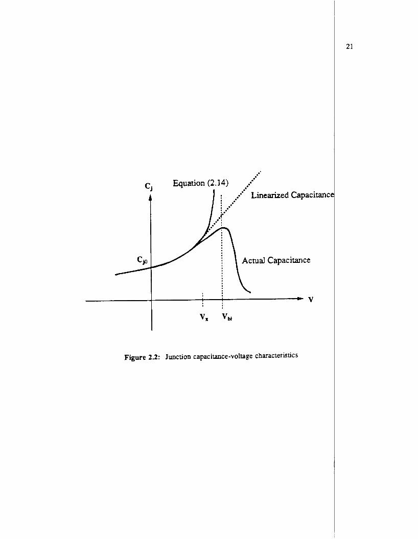
Figure 2.2 : Junction capacitance -voltage characteris tics
21
22
is made of the linearized characteristics. However, this still predicts an increas in the
depletion-region capacitance whereas the capacitance decreases for higher forwar biases
as shown in Figure 2.2 [2.15]. 1 For MOSFETcapacitance models, the application of incrementalcharge p ‘tion-
ing provides correct results only for capacitances connected between the gate con ct and
any of the other contacts 12.45). However, there is no rigorous basis for partition g the
channel charge between the drain and source terminals. The partitioning that is sually
performed is arbitrary and is only motivated by physical operation of the device. There
is no theoretical justification that one particular charge-partitioning scheme is bett r than
another [2.32]. Ward I2.441 has developed a channel-charge partitioning scheme that is
used in several MOSFET models. This partitioning scheme leads to nonreciproca capa-
citances and the source-drain and drain-source capacitances are negative I2.321.
~
The capacitance models are based on a low-frequency analysis or the quasi-static
assumption. A mathematical analysis in [2.45] indicates that t h i s approach is not valid
at high frequencies. Thus, low-frequency models do not suffice for high-fr uency
operation or operation under fast transient conditions. 9
If a charge-storage model is based on capacitances, it can lead to nonconsevation
of charge during a transient simulation. It has been shown that a charge-based mbdel is
essential for conserving charge I2.12, 2.311. Therefore, analytical models frequen y use
closed-form expressions to relate the charges to the terminal voltages. The incre ental
capacitances are derived from the charge expressions for experimental verificatio . All
experimental device data are based on capacitance measurements since measure ent of
charges is difficult. However, the capacitance data are obtained from low-fr uency
measurements rendering them useless for high-frequency operation of the device.
Charge storage of minority carriers is important in diodes and bipolar lran istors.
The removal of the stored charge results in a delay when the device is turned off and is i
of concern in switching circuits. Minority carrier charge stomge is modeled by
an effective transit time in a chargecontrol representation of the diode or bipol
tor [2.48]. For the low-frequency or quasi-static model the charge storage is gi
product of the transit time and the current., and the associated capacitance is
difusion capacitance I2.481. At frequencies higher than the reciprocal of
time, the frequency dependence of the diffusion capacitance is important; the
capacitance decreases as the frequency increases [2.49]. Commonly availa
analytical models use a constant value of the diffusion capacitance for all
and are inaccurate at high frequencies.
Even if the analytical model works well under dc conditions, the transie
may be questionable for some regions of device operation. The problems w
the existing analytical models are now summarized. A detailed comparison of
and numerical models is provided in Chapter 7 and substantiates some of the
outlined here.
The diode models do not account for conductivity modulation [2.50]
level-injection conditions. Furthermore, the charge-storage model is inadequ
the turn off of diodes which is important for the study of power-diode circuits.
Bipolar transistor models are inaccurate for operation under high-le
conditions in the collector region, Le., when base pushout occurs I2.49, 2.5
charge stored in the collector region is not properly modeled the delay pr
In MOSFET modeling the capacitance models are also based on a
analysis. Recent attempts in modeling have addressed this problem [2.34, 2.351;
models effectively solve a one-dimensional electron current-continuity equation
the turn off of the transistor would be inaccurate. Attempts have been made to
the Gummel-Poon bipolar model to take into account the base pushout in
pas:-static
these
for n-
All these models, however, make use of low-frequency capacitance models. I

24
channel MOSFETs. There appears to be no simpler way to model the nonq
operation and hence quasi-numerical approaches are used. Most MOS models
of a scheme for channel-charge partitioning which is somewhat arbitrary
sound theoretical basis. This can lead to errors particularly in circuits
charge that flows out of each terminal must be accurately modeled. In spi
these shortcomings analytical models have been and are extremely us
design. If a circuit designer is aware of the limitations of the model, he/s
circuit ensuring that devices never operate in regions which are not ade
by the model in use with the circuit simulator. I
I 23.2. Empirical or Table Models
As the name suggests empirical models are not based on the physical opera ‘on of
the device. These models are based on the terminal characteristics of the devicd; and,
therefore, they can be expected to be technoloa independent when compare41 with
analytical models. The basic idea in a table model is to store a set of discrete ta, for
the current-voltage and charge-voltage characteristics, in multi-dimensional arr ys or
tables. The model-evaluation subroutine of the circuit simulator then interpolates b tween
the discrete values that are stored to obtain the current and conductance value (i for a
given set of terminal voltages. Table models have been commonly used for model ng the
dc characteristics of a device. These models ensure accuracy in the current- oltage
characteristics, but in general do not address the accuracy in conductances whic is of
concern for analog circuits. The models are very efficient since no complex ction
evaluations are required; only simple arithmetic operations have to be performed t com-
pute the conductance and current values.
1
1 1
(P 4
Table models have been successfully used for the simulation of MOS
I2.51, 2.52, 2.531. However, they have not been used for simulation of bipolar tr
circuits because of the exponential nonlinearity in bipolar devices.
The accuracy of a table model depends upon the number of data points SI
the tables. If a large number of discrete data points are stored, the table model w
very accurate. Various approaches have tried to reduce the dimensions of the I
by use of a smaller number of tables and by modeling some dependencies with
cal expressions [2.51, 2.523. The dependency on device sizes is incorporated
tables. Therefore, different tables have to be used for different device sizes. Thi!
a restriction on the device sizes that can be used in simulating a circuit The
table models differ in the way in which they interpolate data; some models jui
use of linear interpolation, whereas others use splines [2.53], or piecewise cubic 1
lation [2.54, 2.551. Alternatively, B-splines can be used for device modeling [2.56
Table models rely on measured data to generate the multi-dimensional table,
current-voltage characteristics; therefore, they can be used only after devices ha7
fabricated with a process. In this mode, table models do not posses any predicth
bility. If use is made of data obtained from device-level simulations, table mod
also be used in a predictive manner. Since table models only need experiment
they are insensitive to changes in technology. In fact, the models do not chang
the underlying process is modified. This is one of the reasons for using a tab1
approach for hardware implementation [2.55].
The use of table models for modeling the intrinsic capacitances of a MOSF
been very limited. In [2.57] the capacitance model is based on analpcal model!
table model is presented in a later work [2.58]. This table model makes 'use of m
capacitance data for generating the charge-based tables. An elaborate inter]
scheme and a fixedcharge partition scheme are used for calculating the capac
However, no circuit simulation examples have been presented with this model, a
not clear if the model consewes charge during transient simulations. An E
25
edin
Id be
lblem
a l p -
I the
Idaces
rious
make
erpo-
If the
been
Lapa-
; can
data,
when
lased
r has
md a
sured
,ation
nces .
I it is
:mate
26
charge-based formulation has been used in [2.59]. A channel-charge partitioning
has to be incorporated in the table model similar to that for analytical modt
capacitance/charge tables are again based OD data from dc characteristics, and ti
are accurate only for low-frequency operation.
Table models are simple, efficient, and technology independent. They are I
general and have been used only for MOS devices. Furthermore, a good table rt
tation for charge is not available from experimental data. Thus, generation of
based table models from experimental data is difficult, and device simulations 1
used. The existing charge-based table models are inadequate for high-frequencj
tion.
23.3. Quasi-Numerical Models
These models make use of the basic physical laws that govern the device
tion. Simplifications are introduced such that the equations can be solved efficic
numerical techniques. The models are referred as quasi-numerical models since c
numerical solutions are not used.
In [2.60] a quasi-numerical model is presented for the bipolar transistor h
one-dimensional expressions for device characteristics are integrated across a dl
yield two-dimensional characteristics. This approach has been successful in mode
two-dimensional operation of the device and is at least an order of magnitude fas
conventional device-level simulation [2.60]. However, the model is a dc model
simple extensions are possible for modeling the transient operation. In addit
model has been derived for a particular type of bipolar device structure, namely
isolated walled-emitter npn transistors.
The simulation program BIPOLE [2.61] uses one-dimensional transport e
with a variable boundary regional approach. Two-dimensional effects are han
;cheme
s. The
erefore
It very
resen-
:harge-
lust be
opera-
opera-
1tlY by
mplete
which
vice to
ing the
cr than
md no
in, the
oxide-
uations
led by

1 27
combining one-dimensional analyses in the lateral and vertical dimensions. Howev
approach is also restricted to a steady-state solution of the device-level equations
time-dependent analysis can be performed.
MOS modeling has been addressed by [2.62] and [2.63]. In [2.62] the dphasis
has been on an environment for developing quasi-numerical models. A model ha
developed only for the threshold voltage of the device. The threshold-voltage
alone is not sufficient for circuit simulation; and, hence, this model is not suital
use in a circuit simulator.
A quasi-numerical model for the drain current is presented in [2.63] along
threshold-voltage model. The drain current is obtained by a numerical solution
one-dimensional currentcontinuity equation. However, both of these approach
limited to dc conditions and are inadequate for dynamic operation of the device.
The non-quasi-static MOS models of [2.34] and [2.35] address the probl
dynamic operation of MOSFETs. The one-dimensional current-continuity equal
solved assuming analytical expressions for the various charges. In this sense
models are quasi-numerical instead of being pure analytical models. The model in
employs a charge-partitioning scheme, whereas the model in [2.35] makes use of
staticcharge models for the gate and substrate currents. Physical effects such as
city saturation are difficult to account for in the models of [2.34] and [2.35].
23.4. Numerical Models
Numerical models employ the solution of the basic physical laws governing
operation for determining the characteristics of a device. This involves a numerica
tion of Poisson’s equation and the currentcontinuity equations; hence, the name n
cal models. These models are accurate and useful for detailed simulations. The
provide a means for predicting the impact of process variations on circuit perfon
been
iodel
e for
ith a
f the
i are
n of
)n is
these
2.341
uasi-
veio-
:vice
solu-
neri-
also
ance.
However, the B U time required with numerical models is prohibitive for use i
circuits. They can be used to advantage in the simulation of leaf cells or small cin
Commonly, numerical models are used to study intemal device operation i
current-voltage characteristics at the device terminals. One of the first app
towards circuit simulation was in the SITCAP [2.64] program, where a one-dime
numerical model for the bipolar transistor is used to generate model parameters
analpcal Gummel-Poon model. The use of numerical models in circuit simulat
been limited to the circuit simulator MEDUSA [2.65]. However, this simulator
available in the public domain; therefore, numerical models have not found widc
use in circuit simulation in spite of the accuracy that they can provide.
28
large
lits .
id the
cation
sional
or the
)n has
is not
;pread
29
CHAPTER 3
An Overview of Device Simulation
3.1. Introduction
The second component of a mixed-level circuit and device simulator is th
simulation capability. The semiconductor device-simulation problem can be
as a set of three coupled nonlinear partial-differential equations (PDEs) in
time, which are obtained from the underlying physics. These equations are
applied terminal voltages which constitute the boundary conditions for the P
ice simulation also relies on physical models for several phenomena and th
common use are described. However, an exhaustive survey of models [
beyond the scope of this chapter. The device-simulation problem can be r
different ways by use of transformations that lead to a new set of basic v
choices are surveyed along with various techniques for scaling the semic
equations.
The continuous device-simulation problem is discretized both in
Space discretization plays an important role in the overall accuracy
Different techniques are available for performing the discretization. Of
difference scheme is described in detail, as this technique has been us
The finite-box and finite-element formulations are also presented for c
problem of automatic mesh generation and grid refinement is then described.
30
After space discretization the device equations result in a system of n
differential algebraic equations. For time-domain transient analysis application
able integration scheme leads to a system of nonlinear algebraic equations.
tions are linearized using the Newton-Raphson technique and solved by
tion or direct methods. Some of the main solution techniques
Small-signal ac analysis is performed on a device by
tions at a dc operating point. The problem is described and
reviewed.
presented.
The operation of a semiconductor device can be described by three fund ental
equations obtained from the Bolt7mann transport equation [3.1]. These are Po’ 1 son’s
32. The Device-Simulation Problem
equation and the electron and holecurrent continuity equations. i
where
V.EE = q(ND - NA + p - n )
1 -V.Jp = -* + (G - R ) 4 at
E = -Vv
J, = - q p , n V v + qD,Vn
Jp = -4 P p P vv - qDp VP
and
(3.la) I

dielectric constant of the material (~cm- ' )
electronic charge (C)
electrostatic potential (V)
electron (hole) concentration ( ~ r n - ~ )
electric field (Van-')
electron (hole) current density (A cm-2)
electron (hole) mobility (cm2 V-' s-')
electron mole) difusivity (cm2 s-l)
donor (acceptor) concentration ( ~ m - ~ )
net generation rate s-l)
net recombination rate ( ~ m - ~ s-')
The solution of the above system of equations provides the internal distribution c
trostatic potential and the carrier densities, and the extemal terminal cumens.
equations cannot be solved analytically; therefore, numerical methods have to bc
The first efforts in numerical solution of these semiconductor device equations dai
to 1964 when Gummel [3.3] solved the steady-state equations in one dimension
bipolar transistor. The solution of the time-dependent problem was presented ir
Solution of the one-dimensional problem was also employed by DeMari for the
state [3.5] and transient analysis [3.6] of pn-junction diodes. The steady-state anc
dependent problems have been solved in two-dimensions by several researchers.
examples of these efforts are the simulation programs PISCES [3.7], HFIELD
BAMBI 13.91, GALENE 13.101, FIELDAY [3.11], and CADDET [3.12]. Recen
has been in the solution of the basic equations in three dimensions. As device
sions are scaled down three-dimensional effects become important. Device-sim
programs that provide three-dimensional analysis are FIELDAY [3.13], TRANAL
31
elec-
bese
used.
back
)r the
[3.4].
eady-
time-
Some
i3.81,
work
.men-
lation
3.141,
32
The modeling of carrier mobilities is important for predicting accurate values
WATMOS r3.151. and CADDETH [3.16].
of the
'33. Physical Models for Device Simulation ! The basic semiconductor device equations rely on physical models for
different quantities, such as the mobilities and the recombination and generatio
The models are used to provide a relationship between these quantities and the
levels, the carrier densities, current densities, and the electric fields. A brief
various models cwently in use is provided here.
in a reduction of the mobility. Different models have been proposed to model the bobil-
ity reduction due to ionized impurities. The first model was proposed by Caugh
Thomas I3.171, where an empirical expression is used that fits the experimental
is given by
where NT = ND + NA is the total doping concentration. Equation (3.3) is used to ode1
the mobilities for both the majority and the minority carriers, although the expr ssion
was originally proposed for majoritycarrier mobilities. Data for the various co stants
appearing in Equation (3.3) is available in the literature for silicon at a temperat e of
300 K; there is no agreement in the literature as to a consistent set of parameters. is is I
possibly due to the differences in processes on which the experimental devices an
cated and in reality the mobility models have to be "tuned" to a process.
Two other models that are in use in device simulators are the Scharfetter-G
model [3.4] and a model due to Arora et al., [3.18]. For the Scharfetter-Gummel
ity model
However, this model is valid only at a temperature of 300 K. The model of Aron
is similar in form to the model of Caughey and Thomas but has a built-in temp
dependence
where To = 300K.
The scattering due to electrons and holes becomes important when the carri
sities are large. One approach to account for caniercanier scattering is to simply
alternate expression for NT of Equation (3.3), namely,
NT=cc(NA + N o ) + (1 - a)(n + p )
where a is assumed to be 0.34 t3.101.
Mobility is also degraded by the electric field. In fact, for large parallel
fields the drift velocity of the carriers saturates and the mobility model must accc
the phenomenon of velocity saturation. Two frequently used models are the Cr
Thomas model I3.171 and the Scharfetter-Gummel mobility model [3.4]. In the
33
rabri-
nmel
lobil-
(3 -4)
:t al.,
ature
(3.5)
den-
se an
(3.6)
zctric
it for
ghey-
)rm er
34
the mobility is expressed as
current-flow direction. A more physical viewpoint requires the use of the quasi-Fenni
level instead of the electric field. However, the differences between use of the electric
field and quasi-Fermi levels is small and the use of El has been preferred [3.1,; 3.101.
For the Scharfetter-Gummd mobility model the electric field dependence is given by I
Another scattering mechanism, that is important in MOSFETs, is surface
to roughness at the silicon-oxide interface and due to interface states.
models for this scattering phenomenon are empirical in nature. The first mobilitylmodel
to account for surface scattering was proposed by Yamaguchi [3.19], where the electric
field is split into two components E l , the component parallel to the current (later# elec-
tric field), and E , , the component of electric field perpendicular to current-flow d ection
(transverse electric field). The mobility is given by
I
T I
I (3.9)
This model was later revised by Yamaguchi [3.20] to a physically acceptable e pirical
model. In this case the mobility is first calculated as m
The above value of p(N, E,) is used in Equation (3.7) or (3.8) instead of p(N).
Selberherr [3.21] has proposed a mobility model for surface scattering tt:
depends on the distance perpendicular to the interface. In PISCES [3.22] use is D
the Watt-Plummer [3.23] model for surface mobility.
33.2. Carrier Generation and Recombination Models
The important recombination and generation mechanisms for silicon are Shi
Read-Hall ( S R H ) recombination, Auger recombination, and avalanche generatioi
recombination rate for the SRH process is given by
where n , p are the electron and hole concentrations, n;, is the effective intrinsic
concentration, '5, (T,,) the electron (hole) lifetime and n, ( P I ) is the concenm
h-aps at an energy level E,. In the SRH recombination process, transitions betwl
conduction and valence bands are assisted by traps in the band gap. Since the
levels of the traps are not known, the most effective trap level is assumed, i.e..
center of the bandgap 13.241. Therefore, n, = p, = n;, .
At higher concentrations the lifetimes decrease due to the creation of ad
recombination centers. The dependence of lifetimes on doping is given by empiric
tions that fit experimental data. A commonly used expression given in [3.25] is
'50
1 +- T =
NT Nref
where NT = No + NA is the total doping concentration. The experimental dat
shows a wide scatter in the various parameters, T~ and N r e f .
35
also
de of
kley-
The
3.1 1)
arrier
in of
n the
iergy
it the
tional
rela-
:3.12)
again
36
where c,, cp are the Augercapture coefficients. The typical values of these constmints
300K are 2.8 x
have a very weak dependence on the doping levels, carrier densities, and temperahre,
m 6 / s and 9.9 x cm6/s, respectively. The Auger coeff
Carrier generation due to impact ionization (avalanche generation) is modeled
GA, = a, I J , I + ap l J p I
The ionization coefficients a, (c$) depend on the electric field accordiig
Chynoweth’s law [3.26],
-B /E, a = a,e
Another recombination process that involves direct band-to-band transiti 11s is b
at
cients
by
(3.14)
to
(3.15)
I I Auger recombination. The model for Auger recombination is given by
where E, is the component of electric field parallel to the current density. The electric
field component perpendicular to the current flow does not cause ionization [3.27 . The
values of impact ionization parameters a$, and B are available in the literature [3.1 I . 33.3. Heavy-Doping Effects
In heavily doped regions of silicon the material becomes degenerate 4 d the
bandgap narrows and becomes position dependent. A simple approach to model b dgap
narrowing and degeneration is by the use of an effective intrinsic carrier concen ation
n, , related to the intrinsic concentration for low doping n, o. f I
1 3.16) - Ul
2 kT ni3 = nio e
where AEg is the effective bandgap narrowing and is determined by electrical m
ments. A frequently used model for is due to Slotboom t3.281,
where E B ~ N = 9mV. and NBGN = 1 x lo” ~ r n - ~ . Since only the total bandgap na
can be determined from measurements it is assumed that the shift in conduct
valence band edges is identical, Le,
The electron and hole concentrations are given by
VT p = ni,e
where 9, ( 4 p ) is the quasi-Fermi level for electrons (holes). Due to the p
dependent bandpap, an additional electric field is created and the expressions for
densities are now given by [3.29]
-.
Once the above physical phenomena have been modeled the basic semiconductc
tions can be solved; the device terminal voltages establish the boundary condit
the PDEs.
37
(3.17)
owing
n and
(3.18)
3.19a)
3.19b)
sition-
wen t
3.20a)
3.20b)
equa-
Ins for
38
The boundary conditions can be classified as Dirichlet or Neumann [3.30 , or a
combination of the two called a mixed-boundary condition. The boundary con 'tions
used in semiconductor device simulation can be classified as physical and artificial boun-
dary conditions [3.1]. The latter boundary conditions have to be imposed to s' ulate d 3.4. Boundary Conditions
only the intrinsic device. I
The physical boundaries are those due to the contacts and interfaces with
or other insulators. The simplest type of contact is an ohmic contact which can
voltage controlled or current controlled. For a voltage-controlled contact the
condition for the electrostatic potential is given by
wc = wo + V q p (3.21)
where yfc is the electrostatic potential at the contact for an applied voltage Vapp Bind ~0 is the equilibrium potential. If the ohmic contact is to a silicon region the bo@dary
values of the carrier concentrations are obtained by assuming thermal equilibri$ and
charge neutrality at the contact. These conditions are given by
np - ni3 = o
No - N A + p - n = O
From these two conditions it can be shown that
WO - VT nC = no = niee
W O
( 23b) I The function s p ( x ) is -1 if x < 0 and +1 if x > 0. Equations (3.21). (3.23t) and
(3.23~) are the Dirichlet boundary conditions for the potential, electron concen
and hole concentration, respectively.
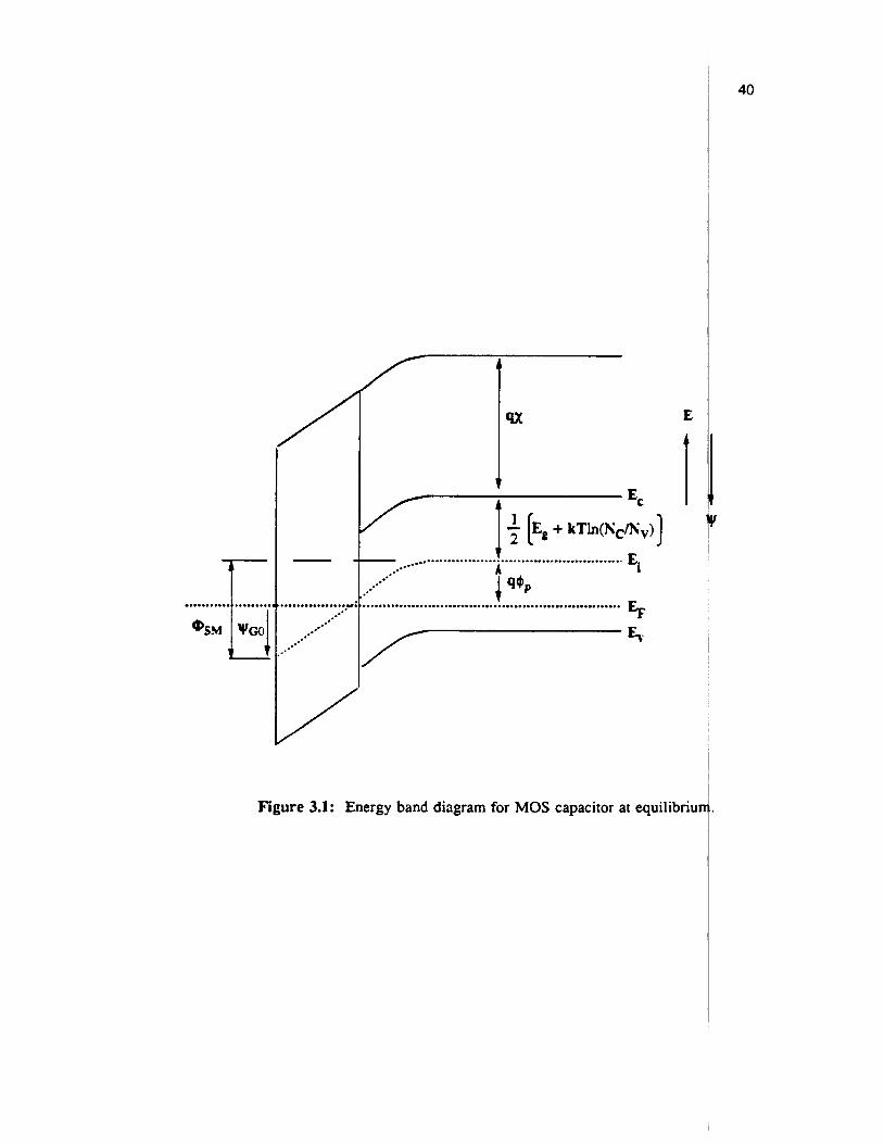
For the gate contact of a MOSFET, \yo has to be evaluated in a different L
To derive the boundary condition, consider the energy-band diagram under qui
for a MOS-capacitor as shown (the substrate is p-type) in Figure 3.1. With the
Fermi level of the substrate as the reference, the gate potential at equilibrium i!
by 9
where mMS is the metal-semiconductor work-function difference, and Op is tk
quasi-Fermi level. With as expressed in terms of the electron affinity x , Equation
can be written as
I- , .-
which can be rearranged to,
where E, is the bandgap, Nc (Nv) is the density of states at the edge of the conc
(valence) band. It should be noted that yg0 from Equation (3.26) can be cal
independent of the doping level in the silicon region, whereas Equation (3.24) r
information of the doping level.
The interface boundary conditions make use of Gauss’s Law in differentia
At the interface,
39
ation,
mer.
brim
luasi-
given
:3.24)
hole
13.24)
:3.25)
:3.26)
iction
ilated
pires
form.
1.27a)
/ r /
'i - ..................................................... .... p q% ..*.
I
EF ...............................................................
Figure 3.1: Energy band diagram for MOS capacitor at equilibriui
40
where Q; is the interfacecharge density. The implementation of this boundary
is described in Chapter 5. The components of current perpendicular to the inkrfwe
given by
Jn *fi = -@SURF
Jp = qRSURF
where h is a unit normal vector, and RSURF is the surface recombination rate. If
assumed to be zero the boundary conditions (3.2%) and (3.27~) reduce to homogeneous
Neumann boundary conditions.
Finally, the artificial boundaries are inserted so that only the intinsic portion
device is simulated. These boundaries have to be determined by the physical operation
the device. For a MOSFET as shown in Figure 3.2 these boundaries correspond
41
coidition
are
43.27b)
(3.27~)
R ~ u w is
of the
of
to the
Naturally, the boundaries A-B, C-D should be placed such that the above con itions
hold good. Otherwise the simulation results would be questionable. E
edges A-B and C-D. At such boundaries it is assumed that the components of
field and current densities normal to the boundary are zero. Thus
E,.fi = 0
J n . A = 0
Jp. f i = 0
The semiconductor device-simulation problem can be solved as given by
(3.1) with y ~ , n and p being the basic set of independent variables. One
this set of variables is that it can lead to negative, unphysical, values for
trations due to roundoff errors. Thus, care must be taken to ensure
3.5. Choice of Independent Variables
dlectric
(3.28a)
(3.28b)
(3.28~)
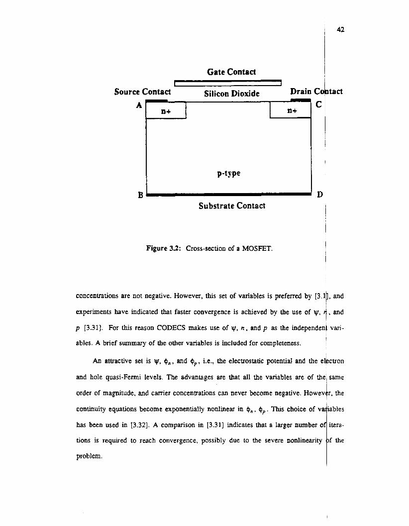
Gate Contact c
Source Contact Silicon Dioxide Drain Cc
B
A
D
1 C
P-tY Pe
Figure 33: Cross-section of a MOSFET.
concentrations are not negative. However, this set of variables is preferred by [3.:
experiments have indicated that faster convergence is achieved by the use of w, ,
p [3.31]. For this reason CODECS makes use of yf, n , and p as the independer
ables. A brief summary of the other variables is included for completeness.
An attractive set is w, +,,, and t$p, Le., the electrostatic potential and the e
and hole quasi-Fermi levels. The advantages axe that all the variables are of thc
order of magnitude, and carrier concenEations can never become negative. Howek
42
continuity equations become exponentially nonlinear in t$n, $I~. This choice of v
has been used in [3.32]. A comparison in [3.31] indicates that a larger number
tions is required to reach convergence, possibly due to the severe nonlinearity
problem.

Slotboom [3.33] has used another set of variables denoted by yf, u , and v ,
kT lq
“i
mwi q lkT
0” VT
-- u = e
kT iq
max IN(x,y)l u max @ , Y ) +
qlkT x max (Dn, D p )
b VT -
v = e
The disadvantage is the large range of values that u and v can take, and this se
ables can also lead to negative values of n and p due to roundoff errors.
3.6. Scaling of Semiconductor Equations
The variables yf, n , p are of widely different orders of magnitude, hence
ice equations have to be scaled in an appropriate manner. The classical scaling ;
was developed by [3.4] and has been widely used. Another scaling that is rigor1
a mathematical point of view is that used by Markowich [3.34]. Finally, a thin
scheme is that used in SEDAN [3.35]. The scaling factors for the three
approaches to scaling are presented in Table 3.1.
I Variables I Scale Factors I DeMari’s 1 Sinpdar Pert. I SI
potential
concentration
length
mobility
VO NO
LO Po
Table 3.1: Various scaling techniques
Based on the above scale factors, the scale factors for the other variable
obtained as in Table 3.2
43
iere
3.29a)
3.29b)
r vari-
: dev-
roach
from
caling
Terent
:an be
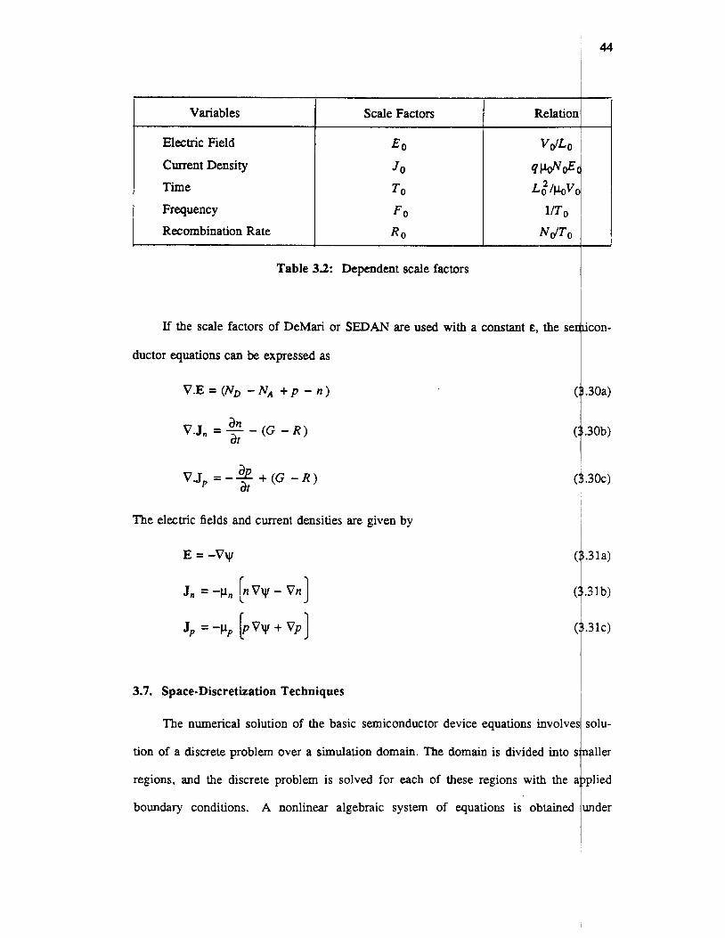
Variables
(3.30a)
(3.30b)
~~~
Electric Field
Current Density Time
Frequency
Recombination Rate
Scale Factors
EO JO
TO
FO RO
Table 32: Dependent scale factors
44
Relation
VdLo
4 W & c L,2/poV0
1lTo
NdTO
If the scale factors of DeMari or SEDAN are used with a constant e, the se 'con- t ductor equations can be expressed as
V.E = (No -NA + p - n)
(G - R ) V.J, = - - an at
V J ~ =-*+(G - R ) at
The electric fields and current densities are given by
E = -Vv
3.7. Space-Discretization Techniques
The numerical solution of the basic semiconductor device equations involve
tion of a discrete problem over a simulation domain. The domain is divided into !
regions, and the discrete problem is solved for each of these regions with the i
boundary conditions. A nonlinear algebraic system of equations is obtained
.3 1 a)
.3 1 b)
.3 1 c)
solu-
ialler
iplied
mder
I
45
steady-state conditions and the unknowns are the discrete approximations to
ous variables. The space discretization can be performed by either a
[3.36] or a finite-element formulation [3.37] and these discretization
For a rectangular mesh with grid spacings hi = x;+1 - xi and kj = Y j + l - 1
described. I
derivatives of a function f ( x , y ) are approximated at grid node (i, j ) shown in 1
3.7.1. Finite-Difference Discretization
The classical finite-difference scheme can be easily applied only to a rec gular
domain. The simulation domain is divided into nonoverlapping rectangular regi ns by
grid lines parallel to the x and y axes. The discretized equations are assembled t each
grid node by approximating the spatial derivatives with difference expressions. this
reason the grid lines should be carefully chosen such that the discrete problem is good
approximation to the continuous problem. I
3.3 by
2
Use of this approximation results in the following discretizations for Poisson's i
current-continuity equations
j , the
3.32a)
3.32b)
kj + -. 2
nd the
3.33a)
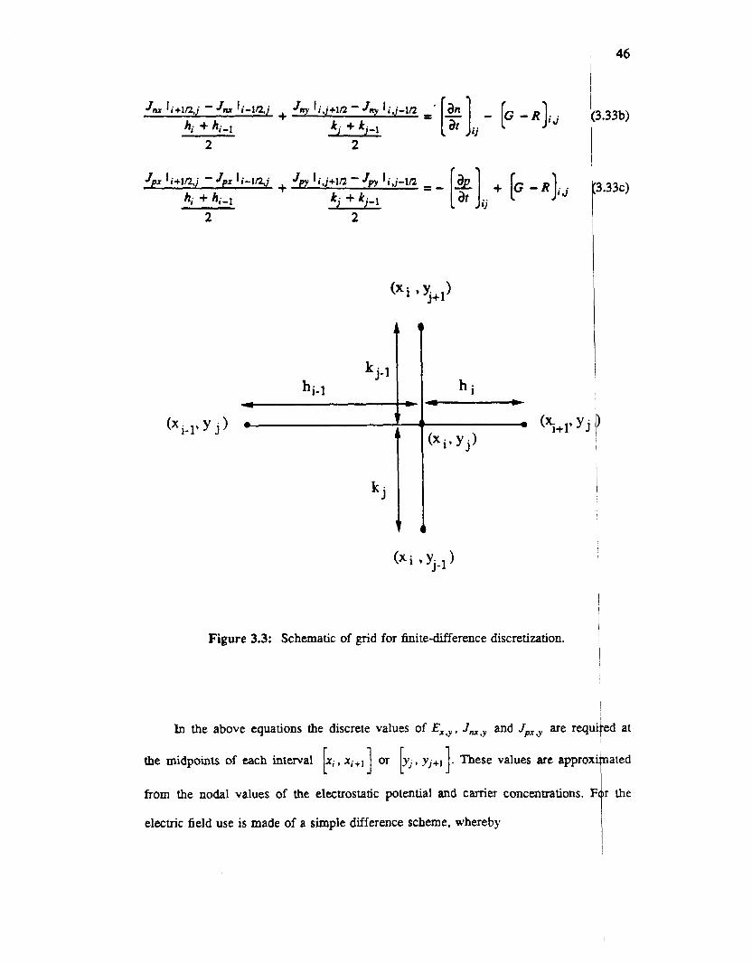
46
3.33b)
3.33c)
(xi 9 ~ j - l )
Figure 3.3: Schematic of grid for finite-difference discretization.
In the above equations the discrete values of Jm,y and Jpx,y are requi ed at t the midpoints of each interval . These values are approx' ated F from the nodal values of the electrostatic potential and carrier concentrations. F r the
electric field use is made of a simple difference scheme, whereby t
This approximation corresponds to the assumption of constant electric field 1
two adjacent grid points. However, a similar difference scheme cannot be used
current densities at the midpoint of an edge, as this scheme is unstable for a I
which the electrostatic potential between two grid points is larger than twice the
voltage [3.38]. Scharfetter and Gummel [3.4] found this instability in the simple
zation scheme and proposed an alternate way for computing the current densitit
scheme can be illustrated by considering the electron current density J , I i + l / 2 j . 1
to be evaluated between grid points (xi, y j ) and (xi+l , y j ) . From the normalize
diffusion equation for electrons
J, = p, nE, + 1 d n l If the electric field, current density, and mobility are assumed to be constant betw
grid points, at their midpoint values, the above expression can be written as
r
which is an ordinary differential equation in the electron concentration n. E
(3.36) can be integrated to get an expression for n ( x , y j ) for the interval [xi
Using the value of n ( x , y j ) at (x i+l , y j ) , one can express J, I i+ln,j as
is the Bernoulli's function. The Scharfetter-Gummel dis where B ( x ) = - e x - 1
X
tion can be used with coarse grids to obtain stable estimates for the current dt
This completes the space discretization of the device equations.
47
(3.34)
.tween
or the
:sh in
lemal
screti-
, This
at has
drift-
(3.35)
:n the
(3.36)
Lation
Xi+] * 1
(3.37)
-etiza-
sities.

48 I
As described, the finitedifference scheme can be applied only to a rectan
and appears to be very limited, since it cannot be used for an arbitrary
domain. Finite-element schemes allow the use of different types of elements
discretization which can be used for arbitrary domains. Extensions of
difference scheme have been made such that it can be used with triangular
discretization is performed by the box integration method. The finite-differen
on triangular grids is used in several device simulators [3.7, 3.8, 3.111. Trim
make it possible to discretize the device equations over an arbitrary simulati
In addition grid nodes can be selectively placed in active regions of the d
box-inteption method for a rectangular grid is described in Chapter 5 , do
discretization of the boundary conditions.
An extension of the finite-difference approach is the method of finite b
method grid points in supe~uous or inactive regions of the simulation do
eliminated by the use of grid lines terminating ir, the interior of the simulation tegion.
Adler [3.39] has used the approach of terminating grid lines in only one directton. A
generalization of this approach, wherein grid lines can terminate in both directions/ is the
method of finite boxes as used by [3.40]. The advantage of the finite-box metho is the
reduction in the number of grid points. However, this is achieved at the expense o addi-
tional storage and elaborate data structures [3.40].
4 f
3.7.2. The Finite-Element Method
The method of finite elements has been extensively applied to problems
tural engineering for several years. However, its application to the problem of
In this method, analogous to the finite-difference method, the domain of
is partitioned into a finite number of nonoverlapping subdomains or
ductor device simulation is fairly recent [3.41].
elements are taken to be triangular or rectangular in shape. Once the elements
selected, an approximation f of the exact solution f is found for each
tial solution for each element is such that its contribution to the complete
solution is zero outside the element. Then, the complete solution is the sum of
solutions over each of the elements,
N
i = l E = I : E i
where N is the number of elements and f i is the partial solution for element i.
The commonly used approximation for f i is a low-order polynomial which
formulated in terms of basis or shape functions as
approximate
partial
(3.38)
can be
where k is the number of nodes in the element (k = 3 for a triangular element and
for a rectangular element), f j are the values o f f at these nodes, that are to be
mined by the finite-element method, and t j are the shape functions. The shape fun
are nonzero over the specified element and zero outside the element. The complete
Let F(w) = 0 denote the basic partial-differential equations for the semiconl
device and G(w) = 0 denote the boundary conditions. Then F(Q and G(?) are the r
tion is then given by
als obtained by substituting the approximate solution into the differential equatior
the boundary conditions, respectively. The next step is to use a sum of inte
weighted residuals of the differential equation and the boundary conditions, and
the sum to zero for a given set of weight functions. This system of equations i
3.39)
= 4
eter-
tions
solu-
3.40)
uctor
sidu-
and
rated
pate
then

solved for fi. If the weighting functions are chosen to be the same as the shap func-
tions the method of weighted residuals is called a Galerkin method [3.42].
One problem with the use of the classical finite-element method when app ied to
semiconductor device problems is the use of low-order polynomials for approx’ ating
the carrier concentrations. The carrier concentrations are exponential functions d this ~
j
results in poor performance of the finite-element method compared to the (finite-
difference method in which Scharfetter-Gummel discretization is used for the 4urrent I
continuity equations. I
I 3.7.3. Gridmesh Generation
In the previous discussion of finite-difference and finite-element methods, a $d is
assumed and the discretization is performed with this grid in mind. The grid shcings
were assumed to be such that the electrostatic potential and the carrier densities c d be
computed accurately from the discretized equations. However, the problem of gri gen-
eration, which involves use of a suitable mesh with the smallest number of grid oints,
was not addressed. With a very large number of grid points a solution with greate accu-
racy can be computed but it requires a significant amount of computational effo It is
for this reason that an efficient mesh is required, which provides accuracy without bxces-
7 1 P
sive computational burden. Heuristics are necessary for the design of a good mes
an appropriate mesh cannot be designed a priori.
In general, adaptive-grid refinement is used to generate an efficient grid dor the
structure to be simulated. The starting point is a grid that resolves the geometry T d the
doping levels in the device. An initial solution is computed on this grid and the error
estimates are computed from the solution. Grid points are inserted in regions wh re the
I
i solution does not meet the user-specified accuracy criterion. The solution has to b inter-
polated for the new grid points that have been inserted. Then the solution is reco puted e
on this new grid and the grid is readapted if the desired error tolerances are not i
or a minimum grid spacing is reached. For certain devices, such as the MOSFJ3
bipolar transistor, a grid can be designed a priori by a knowledge of the operatic
device. In other situations, such as latchup, adaptive-grid refinement is a mus
adaptive-@d generation strategies tend to align the grids with the current-flow
[3.43 J.
3.8. Solution Methods for Device Equations
The techniques used to solve the device-level equations for dc, transi
small-signal ac analysis are described in this section. After space discretization, tl
tions at a grid node i can be expressed in symbolic form as
Poisson’s equation: F,; = O
n-continuity equation: Fni - [$I = o 1
p-continuity equation: Fpi - 1% J = 0 I
The complete system of equations when assembled can be represented in a gene
as
F(w(r), w(t)) = 0
where w is the vector of electrostatic potential, electron concentration, and hole
tration at each grid node.
51
:hieved
md the
of the
Some
rection
zt and
: equa-
:3.41a)
3.41b)
:3.41 c)
1 form
(3.42)
oncen-
3.8.1. Dc and Transient Analyses
After space discretization, a system of nonlinear differential-algebraic q u a t
obtained for transient analysis; for dc analysis this reduces to a system of nonlinear
braic equations. The system of nonlinear equations obtained from dc analysis
solved by a direct method using a Newton scheme. This method is the best from
formance and convergence point of view [3.31]. However, it requires a large amount
storage and computational effort, since a large system of equations has to be
Thus, efficient ways of solving the above nonlinear problem are currently under
gation.
The very first numerical solution of the semiconductor device equations
Gummel [3.3] made use of a relaxation-based approach. The equations are solved
of nonlinear relaxation. This method can be explained by assuming the variables
y!, f),, , qP . Let the nonlinear system of equations be expressed as
43.43c)
ons is
alge-
can be
a per-
of
r;,olved.
hvesti-
h e to
by use
to be
then Gummel's algorithm can be described as follows. Equation (3.43a) is sol*d for
t#+ l with the values of f)n and
t#+' is used in Equations
The whole process is
from the previous iteration. The computed
has been obtained for yr, O n , and t$p. Each equation is nonlinear and Newton's
Gummel's method works well under low-level injection conditions when
equation is effectively decoupled from the current-continuity equations.
high-level injection conditions Poisson's equation becomes strongly
is used to solve the nonlinear system of equations.
continuity equations; the mobile charges affect the electric field distribution. Unc
conditions the relaxation method has extremely slow convergence and may r(
very large number of iterations to reach convergence. From a performance point
this method loses its advantage under high-level injection conditions and cannot
for device-level simulations employing arbitrary bias conditions.
Two modifications have been proposed for Gummel’s method which ensu
convergence under high-level injection conditions. The first method referred to a
simultaneous relaxation (QSR) [3.44] has been applied to the simulation of M(
operating under strong inversion. This is again a condition under which GL
method has very slow convergence. In QSR, Poisson’s equation and the one-dimr
currentcontinuity equation for the carriers in the channel are solved in a
manner. Then the electron and hole continuity equations are solved as in the
Gummel’s method. This method inherently takes into account the coupling of PI
equation with one continuity equation; thus, the nonlinear relaxation is acceleratec
The other approach [3.45] considers a partial coupling between Poisson’s e
and the current-continuity equation for the carrier that dominates the current flc
coupling of Poisson’s equation to the other continuity equation is iporec
Gummel’s method. As a consequence of the assumption that one carrier contril
the total current flow, the above approach is useful for onecarrier simulation 0:
FETs or of highly asymmetric pn-junctions. It cannot be applied for the simul
bipolar transistors, where current flow is due to both carriers under high-level i
conditions.
an For transient analysis, the terms - and .!k have to be discretized in time.
done by use of an integration formula as in the circuit-simulation problem desc
Chapter 2. Some device simulators use semi-explicit integration methods so
at at
53
r such
uire a
view,
: used
better
quasi-
FETs
unel’s
sional
upled
:gular
;son’s
lation
. The
as in
tes to
MOS-
on of
ec tion
’h is is
led in
at the
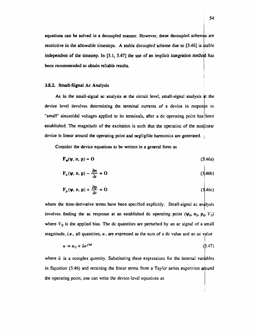
54
equations can be solved in a decoupled manner. However, these decoupled
restrictive in the allowable timesteps. A stable decoupled scheme due to
independent of the timestep. In r3.1, 3.471 the use of an implicit
been recommended to obtain reliable results.
3.8.2. Small-Signal Ac Analysis
As in the small-signal ac analysis at the circuit level, small-signal analysis t the
device level involves determining the terminal currents of a device in respo e to
"small" sinusoidal voltages applied to its terminals, after a dc operating point has t been
established. The magnitude of the excitation is such that the operation of the nonlinear
device is linear around the operating point and negligible harmonics are generated.
Consider the device equations to be written in a general form as I
F,,,(w, n, p) = 0 (3/.46a)
(3146b) I an F,(y, n, P) - at = 0
( .46c) 1 where the time-derivative terms have been specified explicitly. Small-signal ac an lysis
involves finding the ac response at an established dc operating point (yr& no, pd Vo) t
where V o is the applied bias. The dc quantities are perturbed by an ac signal of a mall
magnitude, i.e., all quantities, u , are expressed as the sum of a dc value and an ac alue 1
7 u = uo + iieiW 43.47)
where ii is a complex quantity. Substituting these expressions for the internal varikbles
in Equation (3.46) and retaining the linear terms from a Taylor series expansion
the operating point, one can write the device-level equations as
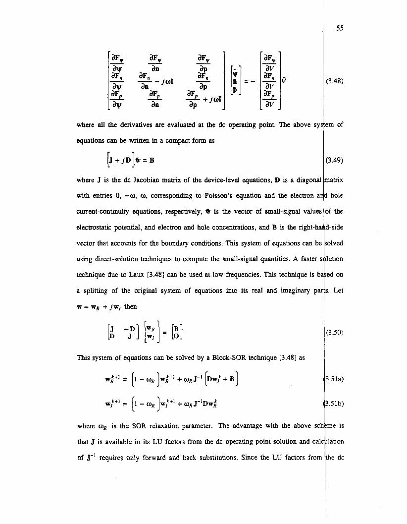
where all the derivatives are evaluated at the dc operating point. The above sy!
equations can be written in a compact form as
[.I + j ~ ] * = B
where J is the dc Jacobian matrix of the device-level equations, D is a diagonal
with entries 0, -0, a, corresponding to Poisson's equation and the electron a
currentcontinuity equations, respectively, fi is the vector of small-signal values
electrostatic potential, and electron and hole concentrations, and B is the right-ha
vector that accounts for the boundary conditions. This system of equations can be
using direct-solution techniques to compute the small-signal quantities. A faster f
technique due to Laux [3.48] can be used at low frequencies. This technique is b,
a splitting of the original system of equations into its real and imaginary pa
w = WR + jwl then
= kl This system of equations can be solved by a Block-SOR technique [3.48] as
where wR is the SOR relaxation parameter. The advantage with the above scl
that J is available in its LU factors from the dc operating point solution and cal
of J-' requires only forward and back substitutions. Since the LU factors from
55
(3.48)
:m of
(3.49)
natrix
L hole
3f the
d-side
;olved
lution
ed on
P. Let
(3.50)
3.51a)
3.51b)
:me is
ilation
the dc
56
operating point analysis can be used to calculate the solution at other frequenci s, this
method is considerably faster than a direct solution of the small-signal equations How-
ever, at high frequencies f > fT 110, where fT is the unity-gain frequency of the evice,
the convergence of the block-relaxation method degrades and at very high frequ cies a
used
to venfy compact circuit-level analytical models. In addition, it provides informa i 'on on
direct-solution method is favored [3.48].
the unity-gain frequency of the device.
Ac analysis at the device level as described above is quite useful. It can
I
CHAPTER 4
Coupled Circuit and Device Simulation
4.1. Introduction
A mixed-level circuit and device simulator should support a variety of anal!
numerical models. It should provide capabilities for dc, transient, small-signal
pole-zero analyses. These analyses must be available for one- and two-dim
numerical devices and, if computational resources permit, even for three-dim
numerical devices. In this chapter the problem of coupled circuit and device six
is addressed. The techniques are applicable to one-, two-, or three-dimensional ni
devices but have been implemented for only one- and two-dimensional devicc
emphasis is on algorithms to couple the device-simulation capability with thc
simulator for dc, transient, small-signal ac, and pole-zero analyses.
The problem of coupled circuit and device simulation is illustrated by an I
of a dc problem. A circuit-level interpretation of the simulation problem prc
motivation for the two-level Newton algorithm. This scheme requires calcul,
linearized equivalent conductances for the numerical devices which are then use
linearized circuit-level equations. It is shown that the linearized conductances
obtained by forward and back substitutions and do not require a large compi
effort.
The two-level Newton algorithm is used to propose an architecture for COUI
device simulator to the circuit simulator. The proposed architecture allows c
57
;es and
LC, and
nsional
nsional
ulation
nerical
;. The
circuit
Kample
rides a
tion of
in the
can be
lational
ing the
)mplete
58
decoupling between the circuit and device simulators; the numerical models are iewed
as another model type from the circuit simulation point of view. The interface ~ ~ w ~ n
the two simulators is well defined and the interface routines necessary for this c upling
A general formulation for the coupled problem under dc conditions is th n pro-
vided, by means of an example. This leads to other approaches for coupling the device
and circuit simulators. In particular the full LU-decomposition technique and.the block-
iterative algorithm used in MEDUSA [4.1] are described. A modification of two-
level Newton algorithm is also proposed wherein a linear prediction is used to pr vide a
better initial guess. The implementation of all four algorithms: (1) the two-level ~ ewton
are described.
algorithm, (2) the full LUdecomposition algorithm, (3) MEDUSA’S block-iterative algo-
rithm, and (4) the modified two-level Newton algorithm, within the framewbrk of
CODECS is presented. It is shown that all of these algorithms can be impleme&ed in
the proposed framework in a decoupled manner.
The convergence properties of these algorithms are then examined for dc anb tran-
sient analyses. A performance analysis indicates that the modified two-level qewton
method is the best for dc analysis, since the other three schemes do not conv+ge on
some benchmark circuits. For transient analysis the full LU-decomposition schbrne is
better from a convergence and performance point of view. The MEDUSA algor@m is
found to be unsuitable for both dc and transient analysis. Some parallelization isdues of
the four algorithms are also presented.
1
The last part of this chapter is devoted to coupling the two simulators
signal ac and pole-zero analyses. Admittances for the numerical devices are
by a numerical small-signal analysis of the device and used in the circuit-level
4.2. DC and Transient Analyses
Since dc and transient simulations are by far the most useful, a major par
chapter addresses algorithms for dc and transient analyses in a mixed-level cir
device-simulation environment. A dc operating point analysis is required beforc
sient run is initiated or for small-signal ac and pole-zero analyses. For this reac
vergence under dc conditions is extremely important; hence, the algorithms usel
analysis must exhibit good convergence properties. The transient analysis prc
better conditioned than the dc problem and solutions from the previous timepoi
vi& a good initial prediction for the solution at the present timepoint. It can b
pated that an algorithm different from the one used in dc analysis may perfom
This section investigates different ways to couple the device and circuit simulatic
bilities for dc and transient analyses. An evaluation is then made on their coni
properties and runtime performance using a variety of benchmark examples.
4.2.1. The Two-Level Newton Algorithm
The problem of mixed-level device and circuit simulation is best illustrate
example of dc operating point analysis. Consider the simple circuit shown in Fii
G is a linear conductance and E, is a dc voltage source. The nonlinear device is
for which the characteristics are specified by a doping profile N ( x ) . The si
problem can be stated as:
Given E,, G , and N ( x )
Find V.
One solution for this problem is motivated by examining the problem fro
cuit simulation point of view. In this case, analytical models are used for the I
devices; the diode terminal characteristics are described by a closed-form ex]
i = I ( V ) . When Newton’s method is used to solve the nonlinear circuit equ
59
of this
uit and
a tran-
Kl con-
for dc
,lem is
~ t s pro-
antici-
better.
1 capa-
:rgence
I by an
ue 4.1.
a diode
ulation
1 a cir-
)dinear
ression,
[ions, a
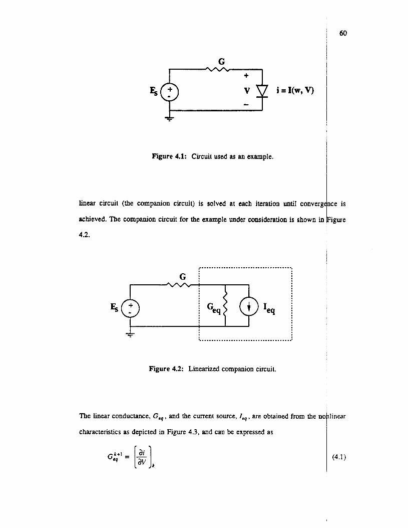
G
-r
i = I(w, V)
Figure 4.1: Circuit used as an example.
linear circuit (the companion circuit) is solved at each iteration until converg
achieved. The companion circuit for the example under consideration is shown in
4.2.
Ice is
?gure
....................................... G i
1 G'q
........................................
Figure 4.2: Linearized companion circuit.
The linear conductance, G,,, and the current source, I e q . are obtained from the no linear
characteristics as depicted in Figure 4.3, and can be expressed as n
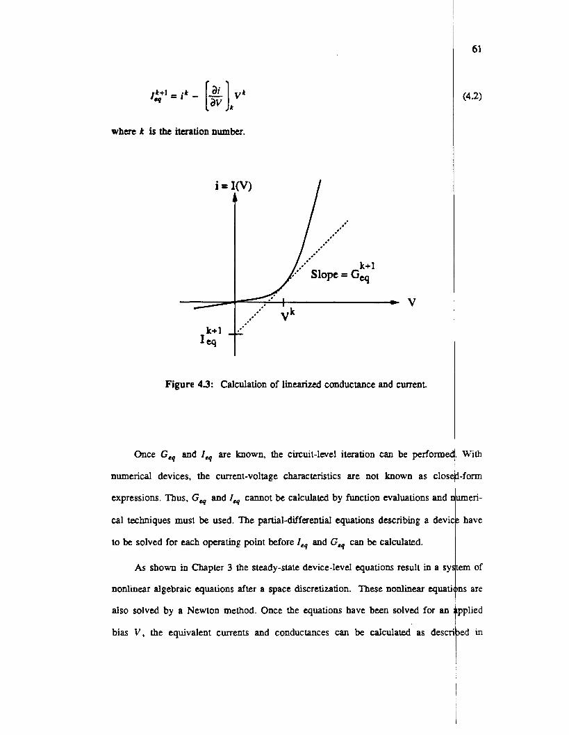
where A is the iteration number.
Figure 43: Calculation of linearized conductance and current
Once G,, and I, are known, the circuit-level iteration can be performed.
numerical devices, the current-voltage characteristics are not known as
expressions. Thus, G, and Ieq cannot be calculated by function evaluations and
cal techniques must be used. The partial-differential equations describing a device
to be solved for each operating point before I,, and G,, can be calculated.
As shown in Chapter 3 the steady-state device-level equations result in a
nonlinear algebraic equations after a space discretization. These nonlinear equations
also solved by a Newton method. Once the equations have been solved for an
bias V, the equivalent currents and conductances can be calculated as described
V
With
closed-form
tumeri-
have
system of
are
r.pplied
in
t'
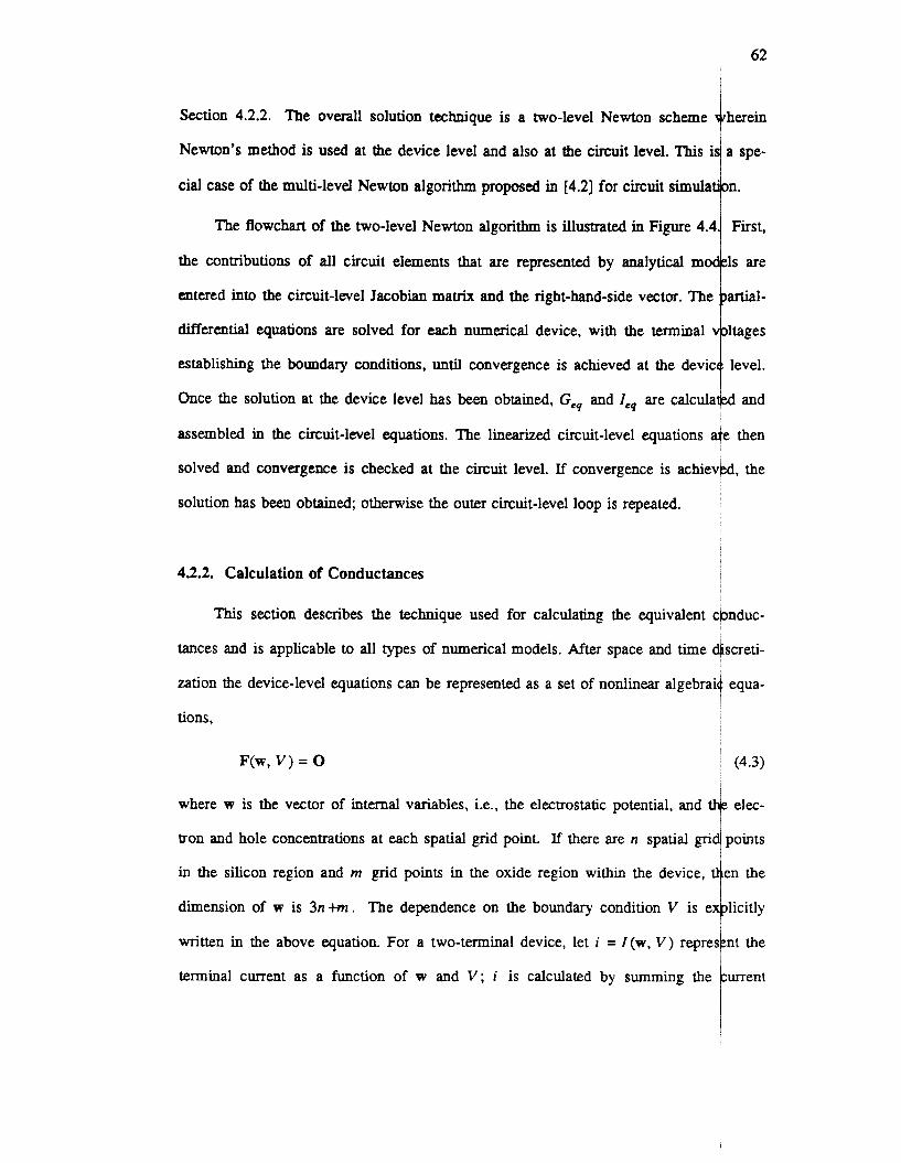
62
Newton’s method is used at the device level and also at the circuit level. This is
cial case of the multi-level Newton algorithm proposed in [4.2] for circuit simulation.
The flowchart of the two-level Newton algorithm is illustrated in Figure 4.4.
the contributions of all circuit elements that are represented by analytical models
entered into the circuit-level Jacobian matrix and the right-hand-side vector. The
differential equations are solved for each numerical device, with the terminal
establishing the boundary conditions, until convergence is achieved at the devic
Once the solution at the device level has been obtained, G, and Icq are calculated
a spe-
First,
are
?artial-
voltages
! level.
and
4.2.2. Calculation of Conductances I
This section describes the technique used for calculating the equivalent cpnduc-
tances and is applicable to all types of numerical models. After space and time qscreti-
zation the device-level equations can be represented as a set of nonlinear algebrai equa-
tions, Q
F(w, V ) = 0 (4.3)
where w is the vector of internal variables, Le., the electrostatic potential, and 9 elec-
tron and hole concentrations at each spatial grid point. If there are n spatial grid1 points
dimension of w is 3n +M . The dependence on the boundary condition V is e licitly
in the silicon region and M grid points in the oxide region within the device,
written in the above equation. For a two-terminal device, let i = I(w, V ) represLnt the ~ the
terminal current as a function of w and V; i is calculated by summing the urrent t
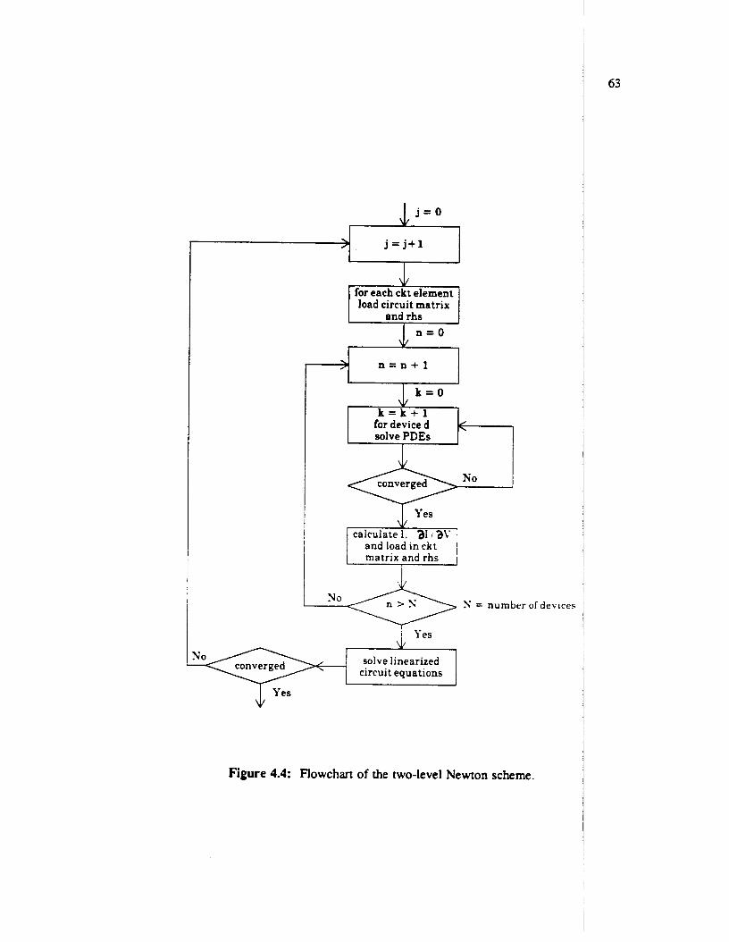
for each ckt element load circuit matrix
and rhs n = O
> n = n + l
k = O
k = k + l for device d < solve PDEs
calculate 1. 21 i a V and load in ckt
solve linearized circuit equations
Figure 4.4: Flowchart of the two-level Newton scheme.
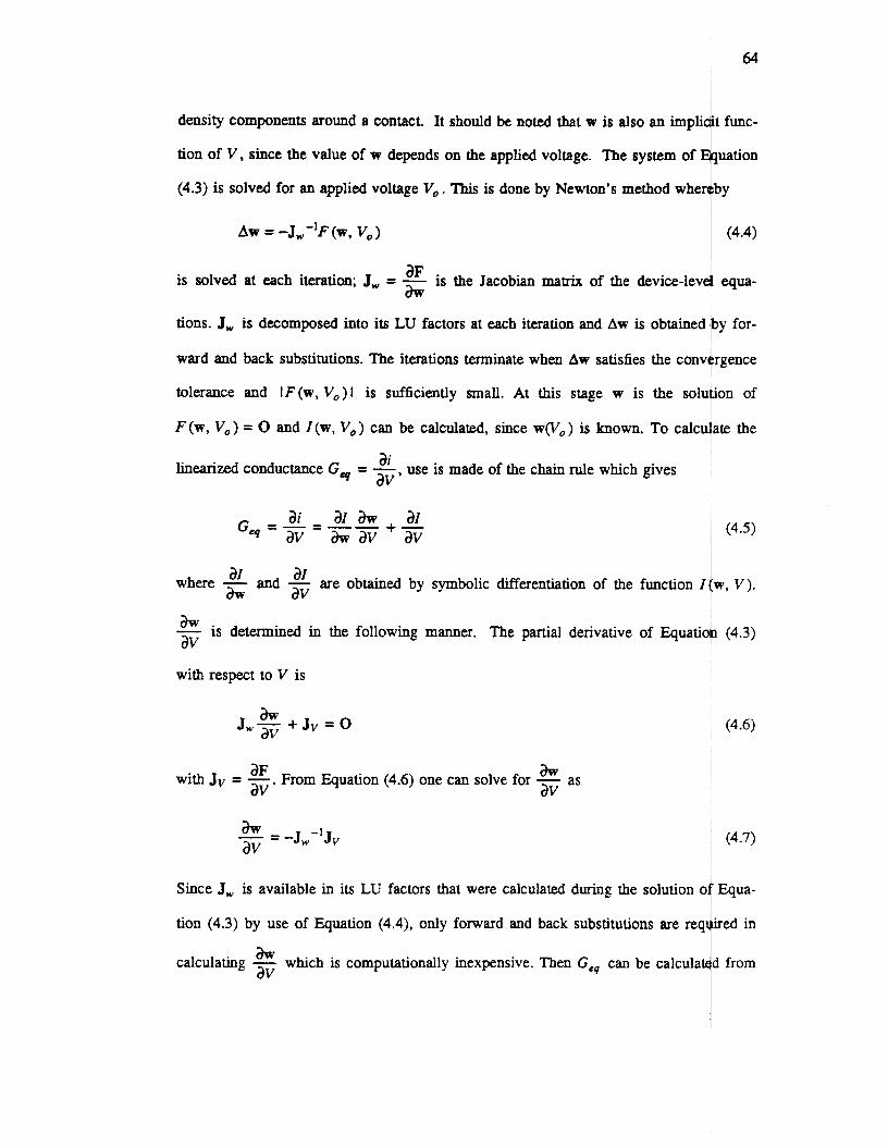
64
density components around a contact. It should be noted that w is also an impli ‘t func-
tion of V, since the value of w depends on the applied voltage. The system of uation
(4.3) is solved for an applied voltage V, . This is done by Newton’s method whe by
4 i (4.4)
is solved at each iteration; J, = - aF is the Jacobian matrix of the device-lev4 equa-
AW = -J,-’F(w, V , )
aw tions. J, is decomposed into its LU factors at each iteration and Aw is obtained by for-
ward and back substitutions. The iterations terninate when Aw satisfies the conv rgence
tolerance and IF(w, V,) I is sufficiently small. At this stage w is the solution of
F (w, V,) = 0 and I(w, V,) can be calculated, since w(V,) is known. To calculate the
linearized conductance G, = - ai use is made of the chain rule which gives
f
av ’
1 (4.5)
I az az aw av and - are obtained by symbolic differentiation of the function I w, V). where -
- aw is determined in the following manner. The partial derivative of Equatiob (4.3) av
with respect to V is
dF aw with JV = -. From Equation (4.6) one can solve for - as av av
aw - = -J,-’Jv av
Since J, is available in its LU factors that were calculated during the solution o
tion (4.3) by use of Equation (4.4), only forward and back substitutions are req
calculating - which is computationally inexpensive. Then G,, can be calculati aw av
(4.6)
(4.7)
Equa-
red in
I from
Equation (4.5).
An alternative way to compute G, is to perturb the terminal voltage Vu bj
amount SV and then calculate the current for the new voltage V, + 6V. G,
puted as
io/, + SV) - i (Vu) 6V
G, =
which is an approximation to 3. This approach is computationally expensive I av two device-level solutions for each bias point. Furthermore, the di
i(Vu + SV) - i (V,) is prone to errors especially when i(V, + SV) and i (Vu) e
to one another, since it involves the difference of two nearly equal quantities. I
difficult to choose an appropriate value of 6V such that the divided-difference
provides accurate results [4.3]. Therefore, the first scheme to calculate conduci
used.
42.3. Architecture of CODECS
It is clear from the previous sections that a numerical device model is simi
analytical device model in several respects for circuit simulation. Given the term
tages the equivalent currents and conductances have to be calculated and use
circuit-level equations. For an analytical model this task involves function eva
whereas for a numerical device the three PDEs have to be solved. The interface
cuit simulator can be identical for the two types of models as shown in Fig
where the task of model evaluation is illustrated. The interface to the circuit sim
through routines for model evaluation, and for loading the equivalent current i
ductances in the circuit-level Jacobian and right-hand-side vector.
65
small
com-
liring
rence
close
; also
heme
:es is
to an
1 vol-
n the
tions,
a cir-
: 4.5,
,tor is
con-
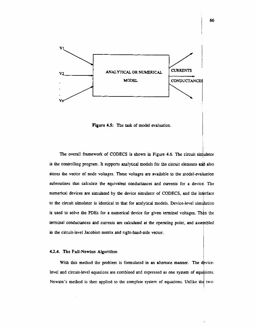
ANALyTlCAL OR NUMERICAL v2 L.
MODEL
Figure 4.5: The task of model evaluation.
CURRENTS
CONDUCrANC c
The overall ,,mework c _ CODECS is shown in Figure 4.6. The circuit s
66
dator
is the controlling program. It supports analyt~cal models for the circuit elements a~# also
stores the vector of node voltages. These voltages are available to the model-ev$tion
subroutines that calculate the equivalent conductances and currents for a device. The
numerical devices are simulated by the device simulator of CODECS, and the in rface
to the circuit simulator is identical to that for analflcal models. Device-level sim4ation
is used to solve the PDEs for a numerical device for given terminal voltages. Thkn the
lerminal conductances and currents are calculated at the operating point, and assebbled
f I
in the circuit-level Jacobian matrix and right-hand-side vector.
4.2.4. The Full-Newton Algorithm
With t h i s method the problem is formulated in an alternate manner.
level and circuit-level equations are combined and expressed as one system of eq
Newton’s method is then applied to the complete system of equations. Unlike
The
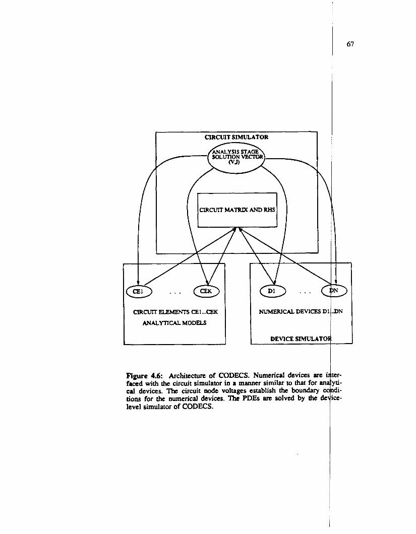
CIRCUIT ELEMpm CE1 ..LEK
ANALYTICAL MODELS
NUMWCAL DEVICES D
DEVICE SIMULATO
Figure 4.6: Architecture of CODES. Numerical devices are I
faced with the circuit simulator in a manner similar to that for an cal devices. The circuit node voltages establish the boundary c tions for the numerical devices. The PDEs arc solved by the de level simulator of CODES.
.DN
ter- yti- ldi- ice-
I 68
a] ai a’ JW-’Jv + - and IT = Z(w, V ) + -A+. Equation (4.15) is with G, = -- aw aw av
level Newton algorithm where the device and circuit-level unknowns are solved
separately in a decoupled manner, the complete set of unknowns is solved s’ ultane-
ously. For the circuit of Figure 4.1, the device-level equations are F(w, V ) =
I
I l o and
these are combined with KCL at the circuit level to get
F(w, V ) = 0
I ( w , V ) + G ( V - E , ) = 0
~ (4.8)
! (4.9)
similar
Equations (4.8) and (4.9) are solved using the Newton-Raphson method.
(4.10)
(4.1 1)
tions to be solved at each iteration of the Newton’s method are then,
J , A w + JVAV = - F(w, V )
a] a1 aw av -Aw + -AV + GAV = - Z(W, V ) - G(V - E , )
From Equation (4.10), Aw can be expressed as ~ ,
AW = Jw-’( -F(w, V ) - JVAV) (4.12)
Equation (4.12) can be rewritten as
Aw = Abi. - J,-’JvAv I (4.13)
where A+ = J,,,-’( -F(w, V)). Substituting Aw from Equation (4.13) into %uation
(4.1 1). one obtains
~ ar JW-’JV + - + G AV = - I(w, V ) - -A* - G (V - E , )
~ (4.14) j
av aw 1 This equation can be rewritten as
G,, + G AV = - IT - G ( V - E , ) [ I (4.15) ~
I
in form to that obtained with an analytical model for the diode or by use of e two- 4
level Newton algorithm. Thus the above technique can also be used to embed DL
models within a circuit-simulation program. The full-Newton scheme can be
mented in two different ways.
42.4.1. Full LU-Decomposition Technique
J, is decomposed into its LU factors and used to calculate A@ and J,'
Equation (4.13) by forward and back substitutions. Then G, and IT are comp
matrix multiplications. Equation (4.15) is solved, whereby AV is obtained and Av
culated from Equation (4.13). using the previously computed values of A@ and.
The equations are solved to convergence. This technique is similar to the use ol
LU decomposition with bordered-block-diagonal matrices in circuit simulation 14.a
42.42. MEDUSA'S Block-Iterative Technique
J, is decomposed into its LU factors; A@, G, and IT are calculated as
Then AV is obtained from Equation (4.15), and Aw is assigned the value of A@.
equivalent to assuming AV = 0 in equation Equation (4.13) and ignoring the c
term due to AV. The equations are solved to convergence. This algorithm is
MEDUSA [4.1].
42.5. Implementation Issues
The three algorithms described above have been implemented in the frame
CODECS shown in Figure 4.5. Tbe interface to the circuit simulator is th:
model -evaluation subroutine which calculates and loads the device contribution
circuit-level equations. The subroutines differ according to the algorithm used
essential features are identical. First, the new voltages are calculated and used t
lish the boundary conditions for the device-level equations; then the device equal
69
lerical
mple-
Jv of
td by
s cal-
-'Jt,.
)lock-
4.51.
Lbove.
'his is
ipling
;ed in
irk of
ugh a
in the
ut the
estab-
ns are
70
solved. This is followed by calculation of the terminal currents and conductances
are then loaded in the circuit Jacobian matrix and right-hand-side vector. The
code for the three algorithms is shown below and illustrates the similarity betwee:)
Furthermore, no algorithm has any significant advantage from an imp1ementatio:i
of view and all three techniques effectively decouple the device-level equations
circuit-level equations. The function setBoundaryConditions is used to establ:.sh
boundary conditions for the device, the function biusSoZution solves the device
to convergence or the iteration limit iterLimit, whichever is reached first. An
value of one allows calculation of A+ of Equation (4.13). The function upduteSolirrion
used to calculate Aw from Equation (4.13) given A+ and AV.
42.5.1. The Two-level Newton Algorithm
which
psP-udo-C
them.
point
from the
the
equations
ircrlimit
is
For the two-level Newton scheme, at each operating point the new term. 1 vol-
tapes (boundary conditions) are imposed on the device and a solution is obtained &or the +
At% is calculated and stored. Before starting the next device-level iteration, Aw is
lated from A+ and AV, and w is updated. The new updated value of w is used
next iteration. This sequence of operations allows a decoupling between the circiit
new bias conditions.
serBoundaryConditions( device ); biasSolution( device, irerLimir );
calcu-
Tor the
and

imposed on the device. However, in the subsequent iterations the subroutine
tion is used to establish the new boundary conditions and to calculate Aw
correct value of w to be used for the new iteration.
ifi predictionstep ) {
) else {
1 biasSolution( device, I );
setBounduryConditions( device );
updateSolution( device );
42.53. Medusa’s Algorithm
Algorithm Med is similar to the two-level Newton scheme except that o
pass is made through the device-level equations for each circuit-level iteration
calculation of conductances and currents is done in a different manner.
setBoundaryCondirions( device ); biasSolurion( device, 1 );
42.5.4. Modified Two-Level Newton Algorithm
From the above pseudo-C code it is seen that the two-level Newton algori
algorithm Med are similar. The difference is that in the two-level Newton
device equations are solved to convergence with a Newton method. A
Newton algorithm can also be used similar to the full LU-decomposition algori
which the device-level equations are solved to convergence. The
algorithm is given as
if( predictionstep ) {
) else {
1
serBoundaryCondirions( device );
updareSolution( device );
biasSolurion( device, irerLimit );
72
It is shown in Chapter 5 that the updareSolun‘on step with a two-level
method provides a linear prediction of the solution at the new operating
modifications described therein are necessary for the algorithm to work
Four possible techniques to couple the device simulator to the
tions.
have been described. These are the
(1) modified two-level Newton algorithm (M2lev),
(4) two-level Newton algorithm (21ev),
(3) full LU decomposition technique (FullLU), and
(4) block-iterative technique of MEDUSA (Med).
The algorithms are now evaluated on the basis of their convergence properties abd run-
time performance.
42.6. Convergence Properties for Dc Analysis.
The convergence properties of these algorithms has been examined by ev+ating
their performance on several benchmark circuits. A short summary of the circ ‘ts and
the numerical models which are used is given in Table 4.1. CODECS input listn/gs and
the details of the numerical models are given in Appendix B.
Y
In Table 4.2 the results for the dc operating point analysis of circuits with one-
dimensional numerical models for the bipolar transistor are given. The results arb given
as the number of circuit-level iterations followed by the total simulation time. A ‘I-’ indi-
cates that convergence was not achieved in 100 iterations. i As can be seen from Table 4.2 the modified two-level Newton
was always successful in finding an operating point, whereas the
full LU-decomposition schemes were only partially successful, and the
Circuit #Nodes #Circuit #Numerical Model #
Elements Devices =QPe Points
4 4 1 BJT 1D 6: 5 8 1 BJT 1D 6, 7 10 6 BJT 1D 6.
10 10 4 BJT 1D 6. 6 8 2 BJT 1D 6'
26 24 11 BJT 1D 6'. 6 7 1 MOS 2D 31 x 5 5 1 MOS 2D 31 x 7 7 1 MOS 2D 21 x
RTLinv
Oscillator vco Invchain
Astable
MECLgate Pass MOSinv ChargePump
Grid
19
19 21
Circuit
RTLinv Oscillator
vco Invchain
Astable
MECLgate
M2lev 21ev FullLU Med
815.0s 8J5.5~ 8J2.42~
814.5s 8J4.9~ 9/2.6s - 8/25s 10116s - 9122s - 9Jlls - 51J81s 51/94s -
Table 4.2: Comparison of iterations and runtimes
algorithm failed the test in all of these cases. This has been found to be true o : ~
examples as well. For this reason CODECS uses the modified two-level Newton
for dc operating point analysis. The modified two-level Newton scheme is
ally expensive compared to full-LU decomposition but is preferred for dc analysis
it has worked well over a wide variety of examples.
other
scheme
computation-
since
74
42.7. Transient Analysis Comparisons
The transient simulation problem is better conditioned than the problem of (imulat-
ing the dc operating point; hence, the algorithm that works best for simulation
operating point may not be optimal for transient analysis. In this section the
rithms are compared on the basis of their performance for transient
simulations are started with the dc operating point of the circuit being
modified two-level Newton algorithm. All simulations have been
check that is described in Chapter 5. The second order
[4.6] is used for time discretization. A starred entry
complete successfully due to a "timestep too small" error, and the result is report with
the latency check turned off. In Table 4.3, the number of circuit iterations are pr sented f for transient analysis of the benchmark circuits.
Circuit
Oscillator vco Lnvchain
Astable
MECLgate
Pass MOSinv
Chargepump
M2lev
16916 5093 1563 5930 2450
236 287
1644
21ev
16916 5109 1578 6305 2450
236 313 1661
FullLU
18333 5864 1716 6369 2609
295 336 1850
Med
23836 7028 2324 9087 3236* 338 533 266 1
Table 4.3: Comparison of number of circuit iterations
The modified two-level Newton algorithm requires the smallest number of
level iterations. The two-level Newton algorithm requires ten percent more iterat
some examples, and the full-LU technique takes approximately twenty-five perce:
iterations compared to the modified two-level Newton method. In all e>
ircuit-
im, in
more
mples
algorithm Med takes the largest number of circuit iterations and in the ME
example the simulation could only be performed by turning off the latency check.
In Table 4.4 are presented the number of timepoints that were a m p
rejected during the transient analysis. It is seen that the timepoints accepted and
are of the same order.
Circuit
Oscillator vco Invchain
Astable
MECLgate Pass MOSinv
ChargePump
M2lev
5274 1366
1099 1161
401 1 17
1473 I198
619 130
82 I 8
95 1 4
497 1 74
21ev
5274 1366
1106 1 161
404118
1583 1 234
619 1 30
82 1 8
10418
497 / 74
FullLU
5274 1361
1125 1176
401 I 1 7
1465 1 181
619 I 3 1
82 1 8 95 1 4
493 1 73
M d
5274 1 3
1093 1 1
410 I 1554 1 2
619 I 82 i
104 I
492 I
Table 4.4: Comparison of timepoints accepted and rejected
The simulation runtimes are presented in Table 4.5. The full LU-decom:
scheme takes the smallest amount of time. The modified two-level Newton schc
an average, is a factor of 1.7 slower than the full LU-decomposition scheme and
cases does even better than algorithm Med. This might appear surprising at first
the modified two-level Newton scheme requires more CPU time for each circi
iteration. However, as seen from Table 4.6, a fewer number of circuit-level iterat
required at each timepoint. Algorithm Med has no apparent advantage; it requirc
computational effort and does not work well with the latency check.
75
,-gate
and
jected
'sition
le, on
some
cause
-level
ns are
more
Circuit
Oscillator
vco Invchain
Astable
MECLgate
Pass MOSinv ChargePump
M2lev
3126
4805
890
2085
3629
1786 1626 7172
21ev
3636
5440
965
2538 393 1
1955 2194 8045
F U U
2352
291 1
514
1230 2121
1059 1155 4039
Med
3123
3901
806
203 1 4577*
1235
1800 5910
Table 4.5: Comparison of total analysis time
Circuit
Oscillator vco Invchain
Astable
MECLgate
Pass
MOSinv
ChargePump
M2lev
3.0 4.0
3.7
3.5
3.8
2.6
2.9
2.9
21ev
3 .O
4.0
3.7
3.5
3.8
2.6
2.8
2.9
FullLU
3.3 4.5
4.1
3.9
4.0
3.3
3.4
3.3
Med
4.2 5.6
5.4
5.1
5.0*
3.8
4.8
4.7
Table 4.6: Comparison of iterations per timepoint
The four algorithms can also be compared on a time per iteration basis. Thi
the raw speed of each algorithm. It is seen from Table 4.7 that on a time per i,
basis the modified two-level Newton scheme is marginally better than the tn
76
i gives
xation
3-level
Newton scheme in all examples, and it is significantly better in the MOSinv e ample. 1 However, the two-level Newton schemes are approximately a factor of two
the full LU scheme and algorithm Med. On a time per iteration basis,
and the full LUdecomposition scheme are almost identical except in the ME(
example. The full-LU scheme requires fewer iterations per timepoint than algoritl
and is preferable since it results in an overall smaller simulation time.
circuit
Oscillator
vco Invcbain
Astable
MECLgate
Pass MOSinv ChargePump
M2lev
0.18 0.94 0.57 0.35 1.48 7.60 5.67 4.36
21ev
0.21 1.06 0.61 0.40 1.60 8.30 7.00 4.84
0.13 0.50 0.30 0.19 0.81 3.60 3.49 2.18
Med
0.13 0.56 0.35 0.22 1.41 3.65 3.38 2.22
Table 4.7: Comparison of time per iteration
42.8. Conclusions on Performance, Convergence, and Memory Requirement
Theoretical results suggest that the two-level Newton and the full-Newton s
have local quadratic convergence. Algorithm Med has been shown to have sup
convergence [4.1]. The practical implementations are in agreement with the the
results; the previous results indicate the higher rate of convergence for the two-le
full-Newton schemes. However, for dc analysis the modified two-level Newton al<
is better in a practical implementation. It has better convergence than the full-:
scheme.
A possible explanation for this is the strong decoupling between the circuit
device-level equations provided by the two-level Newton scheme. In transient i
the matrices are better conditioned and all schemes can be used. However, the f
decomposition algorithm requires the smallest amount of simulation time
77
L gate
n Med
hemes
rlinear
iretical
el and
3rithm
ewton
nd the
la1 y s is
I1 LU-
nd is,
I
therefore, most suitable for transient analysis. The modified two-level Newton
could also be used for transient analysis but there is a speed penalty of a factor
compared to the full LUdecomposition technique. From a performance and
gence point of view, MEDUSA'S algorithm has no advantage.
An argument in favor of the MEDUSA algorithm is a smaller memory
[4.1] since the coupling terms in Equation (4.13) are not stored. This, however,
a slower convergence. For a mixed-level device and circuit-simulation environme:it
capabilities to simulate devices with at most four terminals (this is typical of
ductor devices), the coupling matrix can be stored as three vectors. In CODECS
been done by temporarily using memory locations that have been allocated for the:
4.2.9. Parallelhation Issues
scheme
of two
conver-
requrement
leads to
with
semicon-
t h i s has
right-
terms of having a higher degree of parallelism.
The task of model evaluation with analytical models has been found to be
parallekable t4.73. In parallel model evaluation each device is spawned off to a
processor and the calculation of conductances and currents takes place in parall
same approach can be extended to numerical devices. Here the model evaluatic'n
highly
different
:1. The
task

involves solution of the PDEs, thus each processor would solve the device equa
parallel with other processors. One could then expect an almost linear speedup 1
number of processors, similar to what has been achieved with the use of BI
models [4.7].
43. Small-Signal Ac Analysis
Ac analysis is useful for analog circuit simulations. Since CODECS is ink
be a general-purpose coupled device and circuit simulator, it also provides a ca
for small-si@ ac analysis. Alternatively, one could run a transient simulati
extract the frequencydomain response using Fourier transform techniques. Howey
approach is computationally expensive and ac analysis provides a good way of 01
the small-signal frequency-domain response.
The ac admittances for each device have to be computed and loaded in th
circuit-level equations. The admittances are functions of frequency, and at a pi
frequency, w, the solution of the algebraic circuit-level equations gives the smal
circuit node voltages and voltage source currents. For analytical device moc
admittances are calculated around an operating point by function evaluations
numerical device the admittances can be calculated at the frequency w by soh
small-sip1 device-level equations as described in Chapter 3. The solution
device-level equations gives the small-signal ac values of the internal variables, t
trostatic potential, and the carrier concentrations at each spatial grid point. Frl
information the ac admittances for a numerical device can be calculated and then
the circuit-level equations.
79
ins in
th the
lytlcal
led to
ibility
1 and
r, this
lining
linear
icular
signal
s the
For a
~g the
If the
elec-
1 this
sed in
43.1. Calculation of Ac Admittances
The small-signal ac terminal current 7 for a device can be expressed as I I
?(0) = j(*(o), Q, 0) (4.16)
where i k is the vector of small-signal values of the electrostatic potential and lectron
and hole concentrations, is the applied small-signal voltage, and 0 is the ra an fre-
quency. The explicit dependence on 0, in Equation (4.16), is through the displicement i
current component of the total current The small-signal ac admittance is given bd I
4 * Y ( 0 ) = Q (4.17)
If is taken to be unity
Y ( 0 ) = i(0)
The small-signal ac current is given by the linear term of the Taylor series exp
i = I (w, V ) around the operating point (w,, V,). Therefore, ~
y ( o ) = i(0) = -ti a + - a] aw av I (4.19)
a1 av and - are evaluated at the dc operating point by use of sfmbolic where - a1
aw differentiation, and C is calculated as described in Chapter 3.
4.4. Pole-Zero analysis
Pole-zero analysis requires computation of admittances for a device as a kc t ion
of the complex frequency s = o + jo. The technique used to calculate the a
for a numerical device is an extension of the method used for small-signal
Instead of using a frequency o, the complex frequency s is used and the
expressed as Y (s). Given a value for s , Y (s) can be calculated and
level equations. The circuit-level transfer function can then be
and zeros can be determined.
For numerical devices Y ( s ) is computed starting from the basic device eq
As in Chapter 3, the unknowns are assumed to be of the form
w = w, + *esf
Using a Taylor series expansion around an operating point and retaining the linea
one can assemble the device-level equations in the form (similar to the equati
small-signal ac analysis given in Chapter 3)
J , + D % = B [ I where J, is the dc Jacobian matrix of the device-level equations, D is a diagonal
with entries 0 corresponding to Poisson’s equation, --s corresponding to the t
current-continuity equation, and s corresponding to the hole current-continuity a
@ is the vector of small-signal values of the electrostatic potential, and electron a
concentrations, and B is the right-hand-side vector that accounts for the boundaq
tions.
The above equations are solved for *(s) by a direct-solution method and thc
is computed by
a1 ar aw av Y ( s ) = -*(s) + -
ar ar aw av where - and - are computed by symbolic differentiation.
4.5. Requirements on Circuit and Device Simulators
The architecture described earlier mandates that the circuit and device sin
possess several basic characteristics. The circuit simulator should allow easy inc
tion of new device models since this capability is used to embed the numerical
81
tions.
4.20)
trmS,
s for
4.21)
iatrix
ctron
ition,
hole
ondi-
Y ( 5 )
4.22)
lators
pora-
vices
82
within the circuit simulator. In addition all the necessary analysis capabilities be
supported at the circuit level of simulation. SPICE3 [4.8] is modular and allows1 incor-
poration of new devices and models. Furthermore, it supports all the important ysis
capabilities at the circuit level. This makes SPICE3 attractive for developing a ed-
level circuit and device-simulation environment. r
The device simulator must be quite general. It should have capabilities for
ing one- and two-dimensional structures and support the various analyses at
level of simulation. Furthermore, it should be able to simulate multiple
to simulate only one device which makes them unsuitable for use in a mixed-leve simu-
lation framework as shown in Fig 4.6. The device simulator should also provide s brou-
tines that compute the terminal currents and conductances of a numerical dev ce for
given terminal voltages. Since many of the above features are not available in I' e isting
opposed to simulating a single device. Most present day device simulators are s
device simulators, a new device-level simulator has been developed for CODECS.

CHAPTER 5
Device-Level Algorithms of CODECS
5.1. Introduction
The algorithms used for one- and two-dimensional numerical device simula
dc, transient, small-signal ac and pole-zero, and sensitivity analyses are describec
chapter. The algorithms at the circuit level are those of SPICE and are not ix
they can be found in [5.1, 5.21.
The first part of this chapter describes the space discretization used in CC
for one- and two-dimensional devices. This is followed by a description of t
boundary condition for a one-dimensional bipolar transistor. The t r a d i t i ~ ~ l
implementing the base boundary condition in a one-dimensional bipolar transisti
to nonconvergence under negative base-emitter voltages. For this reason a differ
mulation has been used which overcomes the problem and in addition provides
physical representation of the one-dimensional bipolar transistor.
Dc analysis is important for finding the steady-state solution of a circuit.
operating point information is necessary for small-signal ac analysis and frequen
as the starting point for transient analysis. However, in the mixed-level envirolu
convergence is a serious problem. The dc convergence problem is examir
approaches to improve convergence in CODECS are described. These include 1
modified two-level Newton scheme with a norm-reducing Newton's method at t h f
level. Device-based limiting along with a voltage-step backtracking scheme ha.
83
in for
n this
uded;
>ECS
base
ay of
leads
kt for-
more
he dc
' used
:nt dc
1 and
! of a
ievice
been

84
I
I j
found to give reasonable convergence.
Transient analysis is extremely important in determining the dynamic responbe of a
error for control of timesteps and integration order. A comparison is made betw n two
circuit. Section 5.4 describes the integration formulae used and the calculation
Latency at the device level should be exploited since the device-level simulation r d e s
a large amount of computational time. As seen in Chapter 4 a full-Newton al rithm
performs the best for transient analysis; hence, the implementation of latency ch k for
the full-Newton algorithm is described. The performance with the latency check i i corn-
different schemes for timestep and order control based on accuracy and perf0
pared with the run times without latency exploitation. Finally, the currentconse$vation
property of the integration formulae has also been examined.
9” local
The algorithms for ac and pole-zero analyses are an extension of the technique for
small-signal ac analysis described in Chapter 3. Some implementation issues are
presented.
The last part of this chapter is devoted to the calculation of sensitivities at dev-
ice level. This results in a capability whereby the sensitivity of device performabce to
process parameters can be determined. Although the effect of process variations $an be
determined by repeated simulations, they are computationally extremely expensive4 Sen-
sitivity calculations are a good alternative. The sensitivity problem is formulated f r both
dc and transient analyses and the implementation details are described. Examples df sen-
sitivities to doping profile variations are also presented.
4
5.2. Space Discretization in Two Dimensions
The fundamental semiconductor equations are Poisson’s equation and the cpen t -
continuity equations. These are given in normalized form (Chapter 3) by
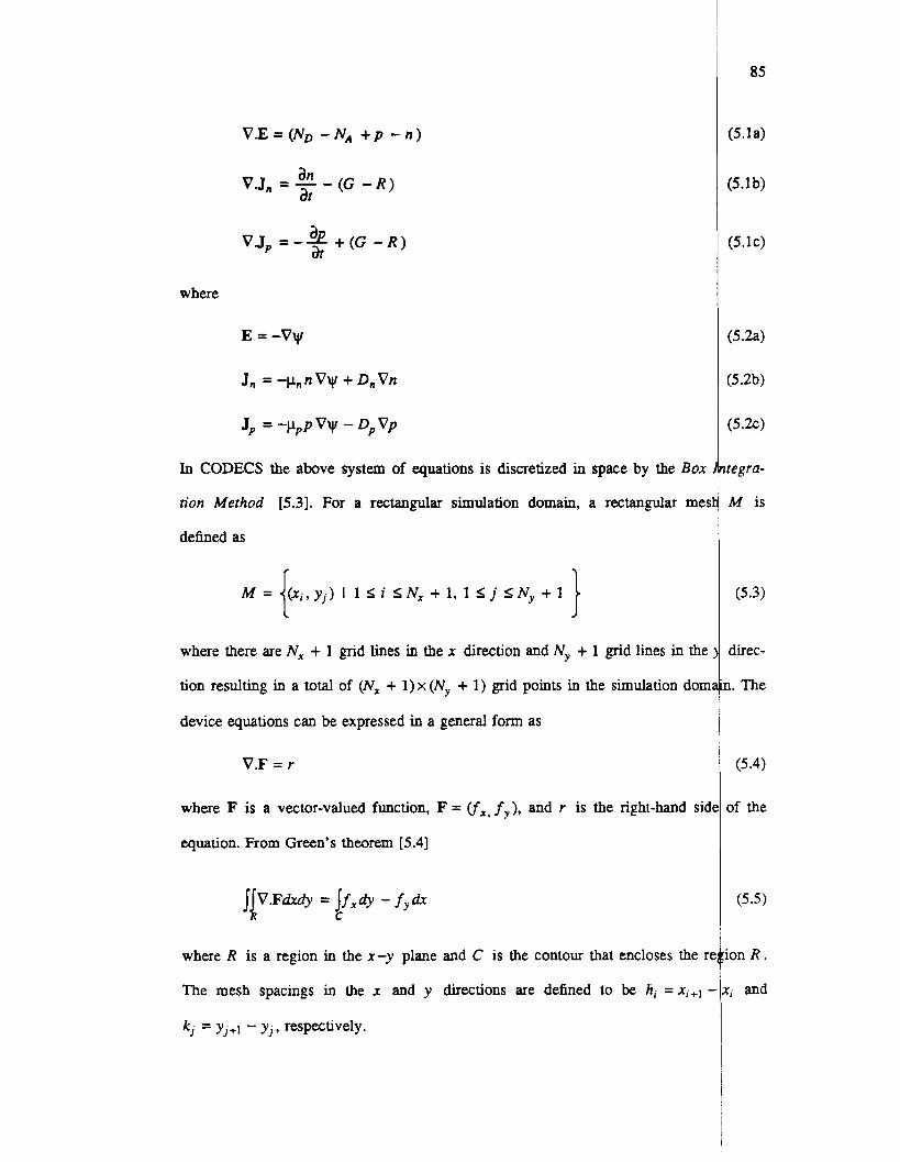
V . E = ( N D - N A + p - n )
where there are N, + 1 grid lines in the x direction and N,, + 1 grid lines in the 1
tion resulting in a total of (Nx + 1) x (N,, + 1) grid points in the simulation domain.
device equations can be expressed in a general form as
V.F = r
where F is a vector-valued function, F = (f,, fy), and r is the right-hand side
equation. From Green’s theorem [5.4]
(G - R ) V . J , = - -
at
an ar
V.Jp =- * + ( G - R )
direc-
The
(5.4)
of the
where
The mesh spacings in the x and y directions are defined to be tij = x i + ] - x i
k j = yj+l - y j , respectively.
J, = -pnnVy + D,Vn
and
(5.lb)
(5.1~)
(5.2b)
J p = -PpPVY - DpVP
In CODECS the above system of equations is discretized in space by the Box
Zion Merhod
defined as
[5.3]. For a rectangular simulation domain, a rectangular mes
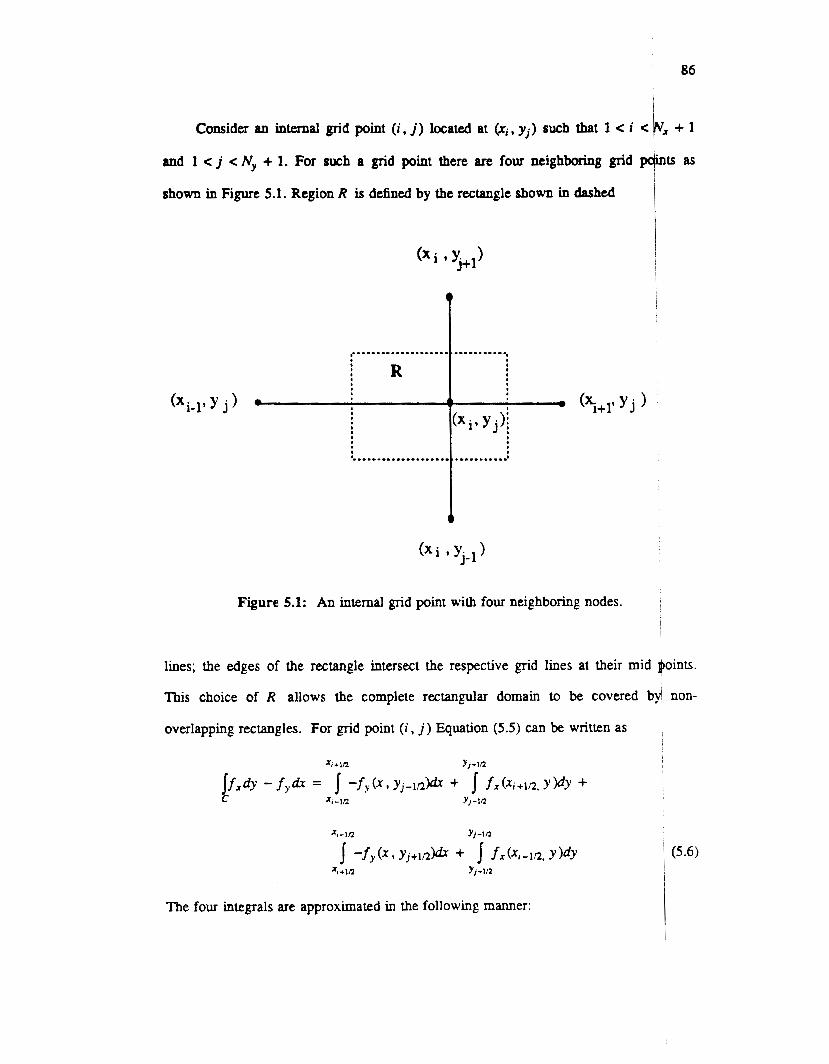
Consider an internal grid point ( i , j) located at (xi , y j ) such that 1 e i <
and 1 < j < Nr + 1. For such a grid point there are four neighboring grid pc
shown in Figure 5.1. Region R is defined by the rectangle shown in dashed
Figure 5.1: An internal grid point with four neighboring nodes.
86
vx + 1
ints as
lines; the edges of the rectangle intersect the respective grid lines at their mid $oink
This choice of R allows the complete rectangular domain to be covered by1 non-
overlapping rectangles. For grid point (i. j ) Equation (5.5) can be written as
The four integrals are approximated in the following manner:
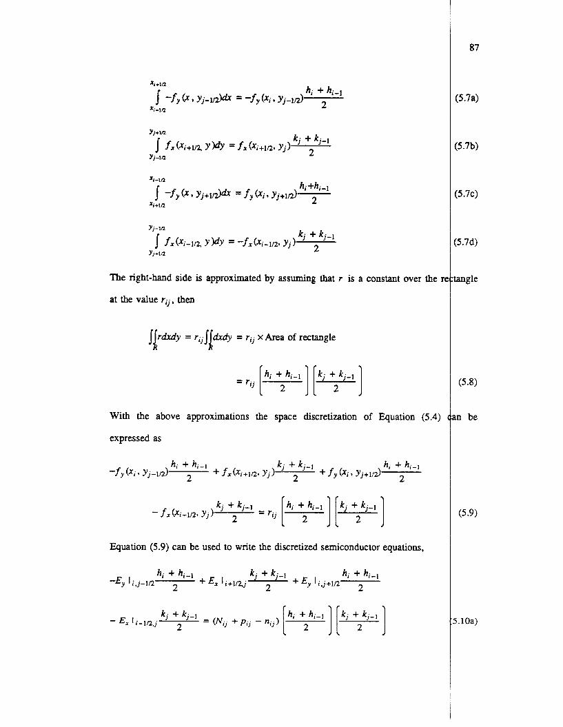
The right-hand side is approximated by assuming that r is a constant over the r
at the value rij , then
y.""y = r , j J l h e = rjj x Area of rectangle
kj + kj-1
With the above approximations the space discretization of Equation (5.4)
expressed as
Equation (5.9) can be used to write the discretized semiconductor equations,
87
(5.7a)
(5.7b)
(5.7c)
5 7 d )
tangle
(5.8)
in be
(5.91
j.lOa)
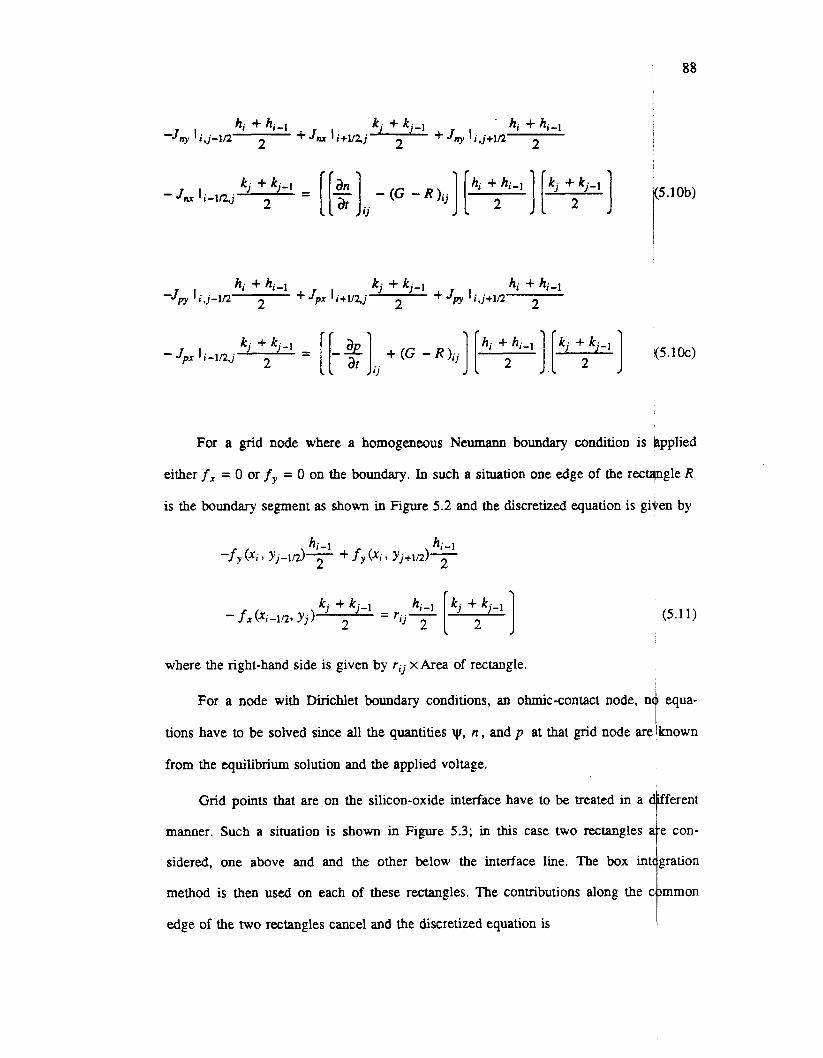
88
1
~ i
I
(5.10b)
I
(5 .10~)
For a grid node where a homogeneous Neumann boundary condition is Bpplied
either f x = 0 or f y = 0 on the boundary. In such a situation one edge of the recwgle R
is the boundary segment as shown in Figure 5.2 and the discretized equation is giiren by
(5.1 1) " 1 J L
where the right-hand side is given by rlj x Area of rectangle.
For a node with Dirichlet boundary conditions, an ohmic-contact node, n equa-
tions have to be solved since all the quantities \y, n , and p at that grid node are l known
from the equilibrium solution and the applied voltage.
Grid points that are on the silicon-oxide interface have to be treated in a
manner. Such a situation is shown in Figure 5.3; in this case two rectangles e con-
sidered, one above and and the other below the interface line. The box int gration
method is then used on each of these rectangles. The contributions along the c mmon
edge of the two rectangles cancel and the discretized equation is :1
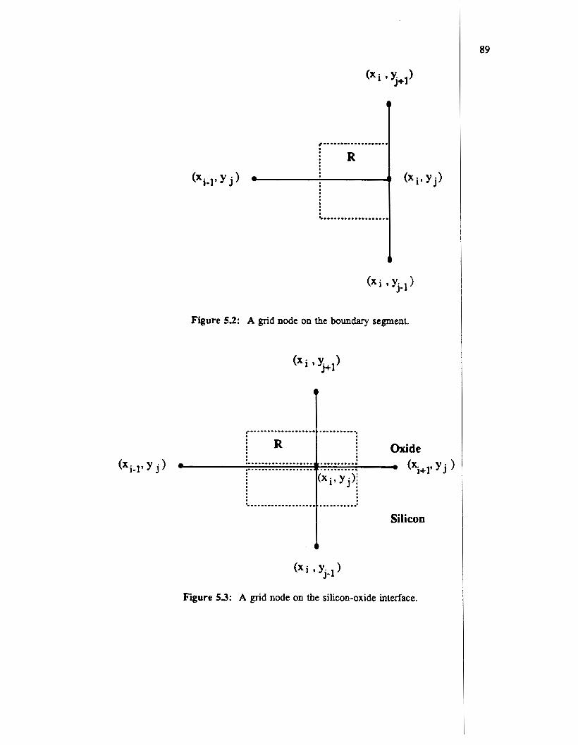
p................. I
i R (xi-]* Y j
C.................
Figure 5.2: A grid node on the boundary segment.
................... (xi-]* Y j 1 ................... I
! I %.*........-.......
Oxide I ........... ........... (x,+]* Yj
x y j);
, ........... Si I i con
(xi ~ j - 1 )
Figure 53: A grid node on the silicon-oxide interface.
89
90
(5.12) I
The above scheme is used for discretizing the Poisson’s equation at the interfahe grid
nodes. Since there is no charge in the oxide region, [r i j ] = 0. Furthermoreb fy is
continuous at the interface if there are no interface charges. Therefore,
OR&
&OX
ES
where E, = -.
As seen from Equation (5.10) Ex,y, JN.s and JPxg involve derivatives of the vari-
ables W, n and p . Approximations have to be made to obtain values of the electric
fields and current densities at the midpoints of each edge since they are requlred in
Equation (5.10). To calculate the electric field values at the midpoint of each d d line,
the potential is assumed to vary linearly between grid points, i.e., the electric fidld is a
constant between two grid points and is given by
i For the current densities at the midpoints use is made of the Scharfetter-Gummel hiscret-
ization, which also makes use of the fact that the electric field is constant betwen two
grid points. Therefore,
,
5.13b) I
is the Bernoulli’s function. As indicated in [MI, Bex where B ( x ) = - ex - 1
X
function has to be evaluated with care and CODECS makes use of the method su
in [5.5].
53. Space Discretization in One Dimension
Analogous to the space discretization for two dimensions, the following dir
tions can be obtained for the semiconductor equations in one space dimension. I
node i located at x i , the equations are
Wi+l - Vi Vi - Vi-1 hi + hi-1 - hi hi-1
53.1. Base Boundary Condition for One-Dimensional Bipolar Transistor
The traditional way of setting the base boundary conditions for a one-dim
bipolar transistor treats the base node as a point contact. To account for the late
current flow in a bipolar transistor a two-dimensional structure must be simulated
ever, it is also possible to do one-dimensional simulations by using a special b
condition for the base node. The quasi-Fermi level of the the majority carrier
base contact is assumed to be equal to the applied base-emitta voltage [5.6]. Thi
tion results in a discontinuity in the current at the base node and the discontinuit
91
5.13~)
oulli ’ s
gested
retiza-
ir grid
5.14a)
5.14b)
5.14~)
isional
11 base
How-
mdary
at the
condi-
equals
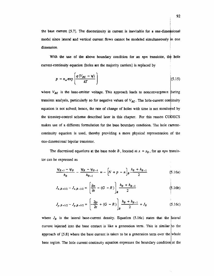
92
the base current [5.7]. The discontinuity in current is inevitable for a one-dime sional
model since lateral and vertical current flows cannot be modeled simultaneously one
dimension.
1 1
With the use of the above boundary condition for an npn transistor, thk hole
current-continuity equation (holes are the majority carriers) is replaced by I
transient analysis, particularly so for negative values of VBE. The hole-current con * uity
equation is not solved; hence, the rate of change of holes with time is not monito ed by
where VBE is the base-emitter voltage. This approach leads to nonconvergence
the timestepcontrol scheme described later in this chapter. For this reason CObECS
makes use of a different formulation for the base boundary condition. The hole cment-
continuity equation is used, thereby providing a more physical representation bf the
one-dimensional bipolar transistor.
r The discretized equations at the base node B , located at x = x B , for an npn t$ansis-
tor can be expressed as
VB+1 -VB VB -VB-l hB hB -1
-
[ 2 (' - R ) ] " + h B - l 2 J n g + 1 1 2 - JnB-112 = - -
B
(p. 16a)
( .16b) I
where JB is the lateral basecurrent density. Equation (5 .16~) states that the
current injected into the base contact is like a generation term. This is
approach of [5.8] where the base current is taken to be a generation term
base region. The hole currentcontinuity equation expresses the boundary
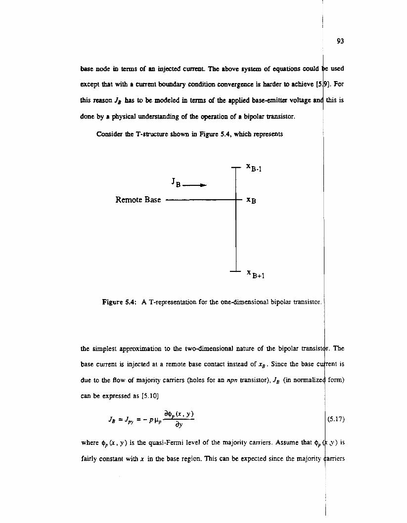
base node m terms of an injected current. The above system of equations could
except that with a current boundary condition convergence is harder to achieve I!
this reason JB has to be modeled in terms of the applied base-emitter voltage an
done by a physical understanding of the operation of a bipolar transistor.
Consider the T-structure shown in Figure 5.4, which represents
where $p ( x , y ) is the quasi-Fermi level of the majority carriers. Assume that $p
fairly constant with x in the base region. This can be expected since the majority
T 'B-1
(5.17)
(.r ,y ) is
camers
JB -
' 'B+1
Figure 5.4: A T-representation for the one-dimensione ipolar transistox
the simplest approximation to the two-dimensional nature of the bipolar transis
base current is injected at a remote base contact instead of x B . Since the base c
due to the flow of majority carriers (holes for an npn transistor), JB (in normaliu
93
: used
1. For
this is
.. The
*ent is
form)
can be expressed as 15.101
94
in the base flow laterally. Furthermore, this has been shown to be a reasonable +sump-
tion by use of two-dimensional numerical simulations [5.11]. Thus,
4 p k Y) = q69 and
Equation (5.19) is now discretized as
(5.18)
1 (5.19)
(5.20)
With the assumption p j + ] s P I j + l R = pB p p B , the base current can be expressed a$
At the remote base contact $, = VeE, then
In normalized form p = nice9pg -'*; therefore, JB can be written as
(5.21)
(5.22)
(5.23)
where Ay is the distance of the internal base node from the remote base contact w d can
be used to model the base resistance of the bipolar transistor. It should be noted @at the
base resistance is conductivity modulated since p B appears in the expression for .IB. I
1 Thus Equation (5.23) provides a physical representation of the bipolar transistor1 and is
used in CODECS. Ay is a user specified parameter and has a default value of Ax . The
above scheme exhibits no convergence problems in all transient one-dimensional
transistor simulations that have been performed with CODECS.
9
5.4. Dc Analysis
At the device level dc analysis involves the solution of the device equatior
applied terminal voltage V. The device equations after space discretization
expressed as
where w(V) is the vector of internal variables corresponding to the applied bias.
tion of these highly nonlinear equations by iterative methods is prone to severe
gence problems. Newton’s method is guaranteed to converge only when the initi
is close to the solution. However, if the initial guess is far from the final soiut
nothing can be said about the convergence of Newton’s method. In order to alley
convergence problem, several modifications and heuristics have to be used ala
the classical Newton’s method. This section describes the enhancements
CODECS to obtain reasonable convergence under dc conditions.
5.4.1. Device-Based Limiting Scheme
Consider the problem of tracing out the dc current-voltage characteristics 0:
iconductor device by use of device-level simulation. The change in the terminal
from one bias point to the next must be small, otherwise convergence is not por
the device simulation. In typical device-level simulations the user specifies the
increments to be used for generating the dc characteristics. In case of nonconi
the user refines the voltage increments to be smaller than tbose used previousl:
by trial and error and by the use of small increments the user can obtain the I
This corresponds to a source-stepping scheme [5.1], the stepping increments fc
are provided by the user.
95
for an
an be
(5.24)
. solu-
snver-
guess
n then
ite the
J with
ed in
I sem-
b g e s
ble in
oltage
*gence
Thus,
lution.
which
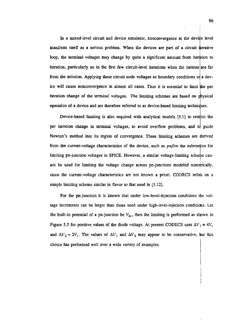
96
In a mixed-level circuit and device simulator, nonconvergence at the devi e level
rative manifests itself as a serious problem. When the devices are part of a circuit
loop, the terminal voltages may change by quite a significant amount from i
iteration, particularly so in the first few circuit-level iterations when the itera
from the solution. Applying these circuit node voltages as boundary condition
ice will cause nonconvergence in almost all cases. Thus it is essential to limit e per
iteration change of the terminal voltages. The limiting schemes are based on hysical
operation of a device and are therefore referred to as device-based limiting techni ues.
Device-based limiting is also required with analytical models [5.1] to res ‘ct the
per iteration change in terminal voltages, to avoid overflow problems, and t , ~ guide
Newton’s method into its region of convergence. These limiting schemes are tlenved
from the current-voltage characteristics of the device, such as pnjlirn the subroupne for
limiting pn-junction voltages in SPICE. However, a similar voltage-limiting sche e can-
not be used for limiting the voltage change across pn-junctions modeled numdrically,
since the current-voltage characteristics are not known a priori. CODECS relids on a
simple limiting scheme similar in flavor to that used in [5.12].
t
4
For the pn-junction it is known that under low-level-injection conditions *e vol-
tage increments can be larger than those used under high-level-injection conditiks. Let
the built-in potential of a pn-junction be Vbi, then the limiting is performed as s$wn in
Figure 5.5 for positive values of the diode voltage. At present CODECS uses AV1 = 4V,
and AVz = 2V,. The values of AVl and AV2 may appear to be conservative, but this
choice has performed well over a wide variety of examples.
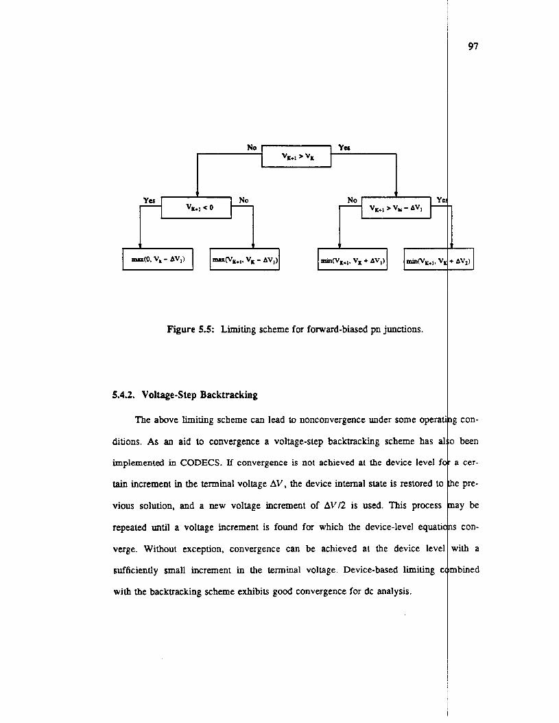
Figure 5.5: Limiting scheme for forward-biased pn junctions.
5.4.2. Voltage-Step Backtracking
The above limiting scheme can lead to nonconvergence under some opera1
ditions. As an aid to convergence a voltage-step backtracking scheme has a
implemented in CODECS. If convergence is not achieved at the device level fc
tain increment in the terminal voltage AV, the device internal state is restored to
vious solution, and a new voltage increment of AV/2 is used. This process
repeated until a voltage increment is found for which the device-level equatil
verge. Without exception, convergence can be achieved at the device leve'
sufficiently small increment in the terminal voltage. Device-based limiting c
with the backtracking scheme exhibits good convergence for dc analysis.
97
4 + AVz)
ng con-
,o been
r a cer-
the pre-
may be
ns con-
with a
lmbined

5.4.3. Linear Prediction of Initial Guess
98
t j
A linear-projection scheme as used in [5.13] is also essential for faster Fnver-
gence. This scheme is derived in an alternate manner here. Consider the devi
equations as in Equation (5.24). These equations are solved by use of Newton’s
whereby, 1
I Aw = -J,-IF(w, V ) l(5.25)
is solved at each iteration until convergence is achieved; J, = - aF is the Jacobiarr of the
device-level equations. Newton’s method requires a good initial guess to ensure Gonver-
gence and the linear prediction step attempts to provide such a guess. The fir$-order
prediction is made by use of a forward-Euler scheme
aw
where AV is the change in voltage from
differentiate Equation (5.24) with respect to V,
from which
- aw = -J,-’ [%] av
(5.26)
aw bias point k to k + l . TO ob*
then
(5.27)
(5.28)
ia aF - has nonzero terms corresponding only to the contact nodes and can be easily ssem-
bled. J, is available in its LU-factors from the solution of Equation (5.24) by use of
Equation (5.25). hence calculation of - requires only forward and back substitutions.
av
aw av
The above scheme does provide a good initial guess as demonstrated b
However, it has also been suggested that convergence is faster if a fraction c
used for predicting the electron and hole concentrations. A typical value sugge
0.7AV. This indicates that a straight-forward implementation of the above sche
not provide a speed up.
A careful analysis of the linear prediction scheme has shown that noncon
may occur when the prediction step results in a negative value for the carrier cc
tions. This is unphysical; therefore, the prediction step has to be modified to prec
sically acceptable values. The improved linear prediction scheme in CODEC!
Fibonacci search sequence to determine acceptable values of An and Ap when
initial values of An or & result in negative carrier concentrations.
The prediction schemes are now examined based on their convergence pr
Since the application is for a mixed-level circuit- and device-simulation envi
these schemes have been evaluated for a dc operating point analysis using the t
Newton algorithm on circuit examples with numerical models for the semiconduc
ices. In Table 5.1 are summarized the results for the classical Newton’s
(NewtonA), Newton’s method with linear prediction (NewtonB), and Newton’s
with improved linear prediction (NewtonC). The numbers are given in the s
number of device iterations, number of circuit iterations, and the runtime in seco
VAX 8650.
The schemes without prediction and with linear prediction have convergen
lems. The Newton scheme with prediction requires a smaller number of deb
iterations on the examples in which convergence is achieved; 36 and 30, respecti
the Invchuin example and 34 and 28, respectively, for the Oscillaror example. T
ton scheme without prediction converges in the MECLgure circuit but does r
prediction is used. This depicts that if the prediction step is implemented wit
99
[5.13].
AV is
:d was
e may
rgence
:entra-
it phy-
uses a
fer the
)erties.
nment,
3-level
)r dev-
nethod
nethod
uence:
Is on a
! prob-
e-level
:ly, for
: New-
. when
lUt any
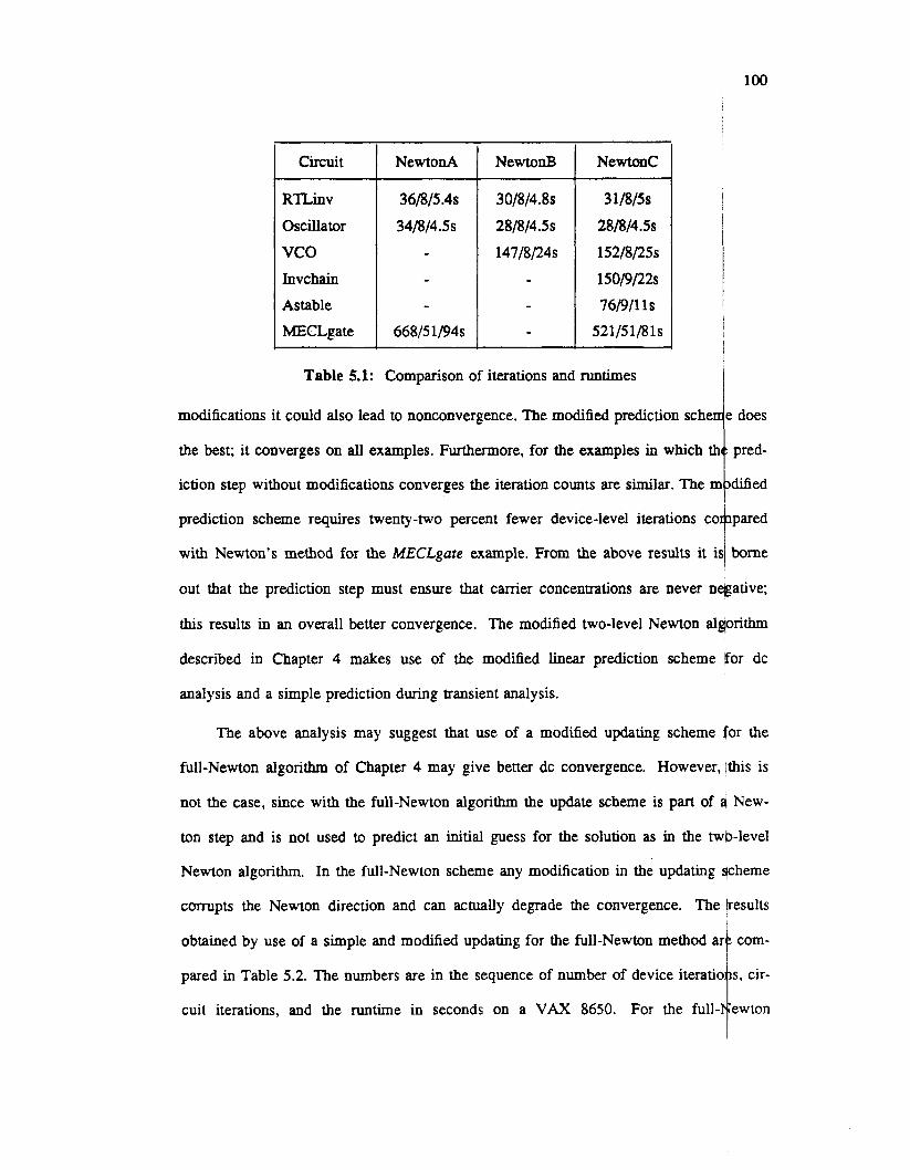
Circuit
RTLinv
Oscillator
vco Invchain
Astable
MECLgate
NewtonA
36/8/5.4s
34/8/4.5s - - -
668/51/94s
NewtonB
30/8/4.8s
28/8/43
147/8/24s
-
NewtonC
31/8/5s
28/8/4.5s
152/8/25s
150/9/22s
76/9/11 s
52 1 /S 1 /8 1 s
Table 5.1: Comparison of iterations and runtimes
modifications it could also lead to nonconvergence. The modified prediction schex
the best; it converges on all examples. Furthermore, for the examples in which tk
iction step without modifications converges the iteration counts are similar. The n
prediction scheme requires twenty-two percent fewer device-level iterations ca
with Newton’s method for the MECLgate example. From the above results it i
e does
; pred-
xiified
npared
borne
out that the prediction step must ensure that carrier concentrations are never n%ative;
this results in an overall better convergence. The modified two-level Newton alworithm
described in Chapter 4 makes use of the modified linear prediction scheme for dc
analysis and a simple prediction during transient analysis.
The above analysis may suggest that use of a modified updating scheme for the
full-Newton algorithm of Chapter 4 may give better dc convergence. However, this is
not the case, since with the full-Newton algorithm the update scheme is part of a New-
ton step and is not used to predict an initial guess for the solution as in the twblevel
Newton algorithm. In the full-Newton scheme any modification in the updating qcheme
corrupts the Newton direction and can actually degrade the convergence. The /results
obtained by use of a simple and modified updating for the full-Newton method ar com- i pared in Table 5.2. The numbers are in the sequence of number of device
cuit iterations, and the runtime in seconds on a VAX 8650. For
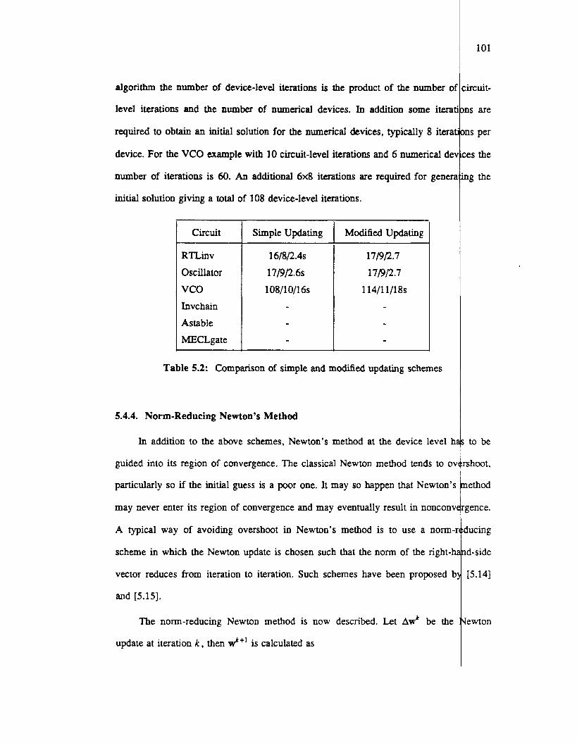
algorithm the number of device-level iterations is the product of the number 01
level iterations and the number of numerical devices. In addition some iteral
required to obtain an initial solution for the numerical devices, typically 8 iterai
device. For the VCO example with 10 circuit-level iterations and 6 numerical de
number of iterations is 60. An additional 6x8 iterations are required for generi
initial solution giving a total of 108 device-level iterations.
Circuit
RTLinv
Oscillator
Invchain
Astable
MECLgate
Simple Updating
16/8/2.4s
17/9/2.6s
108/10/16s - -
Modified Updating
17/9/2.7
17D12.7
11411 1/18s
- -
Table 5.2: Comparison of simple and modified updating schemes
5.4.4. Nom-Reducing Newton’s Metbod
In addition to the above schemes, Newton’s method at the device level b
guided into its region of convergence. The classical Newton method tends to 01
particularly so if the initial guess is a poor one. It may so happen that Newton’s
may never enter its region of convergence and may eventually result in nonconv
A typical way of avoiding overshoot in Newton’s method is to use a norm-
scheme in which the Newton update is chosen such that the norm of the right-h
vector reduces from iteration to iteration. Such schemes have been proposed t
and [5.15].
The norm-reducing Newton method is now described. Let A d be the
update at iteration k , then d+’ is calculated as
101
ircuit-
ns are
ns per
es the
ig the
to be
shoot,
iethod
gence.
iucing
d-side
[5.14]
ewton
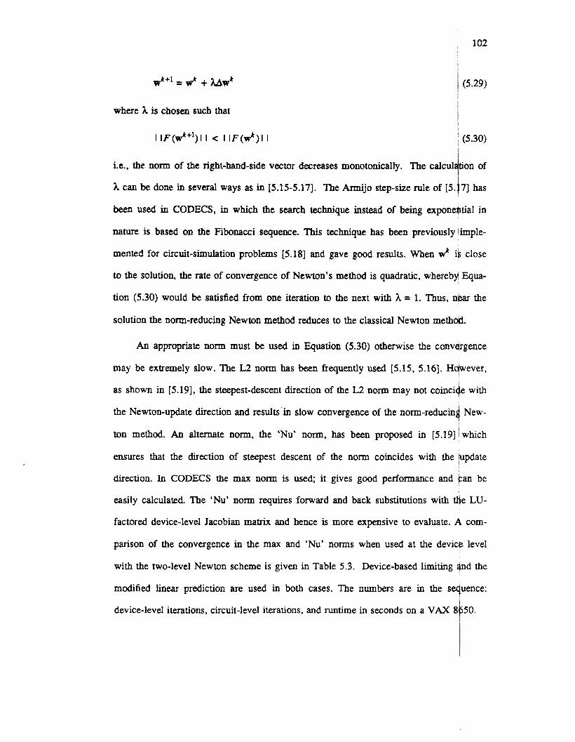
102
h
= d + UW' 1 (5.29)
I where h is chosen such that
1"'" I lF(d+*)l I < I I F ( d ) I I
Le., the nom of the right-hand-side vector decreases monotonically. The calcul tion of
h can be done in several ways as in 15.15-5.171. The Annijo step-size rule of IS. 73 has
been used in CODECS, in which the search technique instead of being exponential in
nature is based on the Fibonacci sequence. This technique has been previously limple-
mented for circuit-simulation problems [5.18] and gave good results. When d i6 close
to the solution, the rate of convergence of Newton's method is quadratic, wherebyi Equa-
tion (5.30) would be satisfied from one iteration to the next with h = l. Thus, n w the
solution the norm-reducing Newton method reduces to the classical Newton methoid.
An appropriate norm must be used in Equation (5.30) otherwise the convdrgence
may be extremely slow. The L2 norm has been frequently used (5.15, 5.161. Hdwever,
as shown in [5.19], the steepest-descent direction of the L2 nom may not coincide with
the Newton-update direction and results in slow convergence of the norm-reducind New-
ton method. An alternate norm, the 'Nu' norm, has been proposed in [5.19]'which
ensures that the direction of steepest descent of the norm coincides with the ppdate
direction. In CODECS the max norm is used; it gives good performance and pan be
easily calculated. The 'Nu' nom requires forward and back substitutions with 4 e LU-
factored device-level Jacobian matrix and hence is more expensive to evaluate. 4 com-
parison of the convergence in the max and 'Nu' norms when used at the devick level
with the two-level Newton scheme is given in Table 5.3. Device-based limiting ijnd the
modified linear prediction are used in both cases. The numbers are in the s uence:
device-level iterations, circuit-level iterations, and runtime in seconds on a VAX 8 50.
9 I I
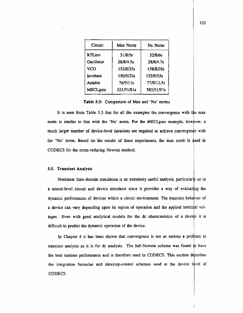
Circuit
RTLinv Oscillator
vco Invchain Astable
MECLgate
Max Norm
3 11815s
281814.5s
152/8/25s
150/9/22s
76/9/11 s
52 1/5 1 /8 1 s
Nu Norm
32/8/6s
28/8/4.7s
158/8/28s
152/9/25s
7 7 m 2.5s
583/51/97s
Table 53: Comparison of Max and ‘Nu’ norms
It is seen from Table 5.3 that for all the examples the convergence with ’
nom is similar to that with the ‘Nu’ nom. For the MECLgare example, hov
much larger number of device-level iterations are required to achieve converger
the ‘Nu’ norm. Based on the results of these experiments, the max norm is
CODECS for the norm-reducing Newton method.
5.5. Transient Analysis
Nonlinear time-domain simulation is an extremely useful analysis, particula
a mixed-level circuit and device simulator since it provides a way of evalua
dynamic performance of devices within a circuit environment. The transient beh
a device can vary depending upon its region of operation and the applied termj
tages. Even with good analytical models for the dc characteristics of a dev
difficult to predict the dynamic operation of the device.
In Chapter 4 it has been shown that convergence is not as serious a prc
transient analysis as it is for dc analysis. The full-Newton scheme was found
the best runtime performance and is therefore used in CODECS. This section c
the integration formulae and timestep-control schemes used at the. device
CODECS.
103
2 max
ver, a
: with
;ed in
I so in
ig the
ior of
11 vol-
: it is
.em in
have
;tribes
vel of
m e nodinear device-level equations after space discretization can be expr+ssed in
the form I
' (5.31) t I
where w is the vector of internal variables and V ( t ) are the applied terminal vbltages.
This system of differential-algebraic equations is transformed to a system of nfnlinear
F 1, w(t 1, v ( t )) = 0
I
b
algebraic equations after discretization in time, i.e., at timepoint I i
$(wn+l) = 0
These nonlinear equations can be solved by Newton's method. The discre
time is done by use of an integration formula which provides an approxima
time derivative of a variable x (t ) at time t,+l in terms of the values of the
tn+l and values of the variable and its derivatives at the previous timepoints.
tistep @-step) integration formulae of order k , that are in common use
aided circuit and device analysis, are given by
(5.33)
where 2p+l-k of the ai and bi are assigned arbitrarily and h, = tn+] - tn . Theirest of
the coefficients are determined from exacrness consnainrs, Le., a kth-order intqgration
formula is exact for polynomials in t of degree less than or equal to k . An intqgration
method is an implicit method when a. # 0. Implicit methods require an iterative golution
must be stiffly stable to be of practical use since the time constants of the equati
but have larger regions of stability and hence are preferred. The integration
s may ~~s
vary by several orders of magnitude [5.1, 5.201. I
Trapezoidal integration has been widely used in circuit simulation [5.1].
A-stable method that has the smallest local error [5 .21] . However, it is not sui
device-level simulation because it is not L-stable [5 .22] , Device-simulation pro
extremely stiff and if the local error is not monitored carefully the results exhibit
an artifact of the integration method. With a proper control on the error, the t
taken may be small whereby there is a restriction on the timestep and no adva
using the trapezoidal method [5.23]. The backward-Euler method has been
several device simulators [5.4, 5.241, even though it is a first-order method ar
large local error. A second-order method that is both A-stable and L-stablc
backward-differentiation formula of second order, BDF'2. Thus, it is well s
device-level simulation problems. However, it also has a local error that is lar,
the trapezoidal method and an alternate integration formula is the TR-BDF2 sche
posed in [5.23]. The TR-BDF2 method requires two solutions for each timepi
first makes use of the trapezoidal integration for a fraction of the timestep a
BDF'2 is used for the rest of the interval. Implementation of this integration sc
CODECS would require modifications to the core of the circuit simulator, which
the simulation. Since the intent has been to keep the circuit-simulation algorith~
tered, the algorithms have to be chosen to ensure decoupling between the cir
device simulators. For this reason the TR-BDF2 has not been considered fc
domain transient analysis in CODECS.
5.5.1. Local Error and Error Estimates
Assume the linear multistep integration method is given by Equation (5.33)
ermore, assume that this equation has been normalized such that C b ; = 1. T
error of the integration method at time point fn+l is then defined as
P
i d
where x (rn+l) denotes the exact solution to the differential equation at tirne I,,
105
nging,
esteps
ige in
#ed in
hasa
is the
ed to
. than
E pro-
it, the
I then
me in
nmols
una1 -
it and
time-
'urth-
local
(5.34)
Thus.
1 06
local error is the amount by which the exact solution fails to satisfy the differenc equa-
tion, Equation (5.33). The above equation can be expanded around tn by use of ITaylor
series. For a kth-order integration method, with the assumption of uniform stepsi+s, the
d
1
local error [5.25] is
k+l k+1 E n + ] = Ck+lh x ( t n 1 (5.35)
where Ck+] is called the mor constant of the integration method. A method of
that has the smallest value of CL+l will have the smallest local error and will
be more accurate. From Equation (5.35) it might appear that by scaling Equati
Ck+, could be reduced thereby reducing the error of the method. However, the vaiues of
x computed from Equation (5.33) will not change; therefore, the accuracy of the method
will not be affected. It is for this reason that the normalization C b , = 1 was intrduced; P
id
after this normalization the constant CC+] is invariant to such scalings [5.25] andl hence
can be used as a measure of the accuracy. The local error for two second-order mdthods,
BDF2 (second-order BDF) and trapezoidal method, is now derived for the cwe of
nonuniform step sizes.
5.5.1.1. Local Error for the BDF2 Integration Method
The BDF2 integration method is given by
where ao, a I and u 2 are obtained from the exactness constraints. Their values are
(5.36)
hn + hn-1 h" -1
a ] = -
where h,= rn+l - r,,. To obtain the error, the exact solution x ( r ) is substituted
tion (5.36)
From a Taylor series expansion around r,. it can be shown that
5.5.1.2. Local Error for the Trapezoidal Rule Integration Method
The trapezoidal method when expressed in the form of Equation (5.33)
P
id normalization x b i = 1 is given by
Substituting the exact solution x (r ) in Equation (5.39), one obtains
From a Taylor series expansion around 1,. it can be shown that
107
(5.37)
(5.38)
th the
(5.39)
(5.40)
(5.41)
108
I
5.5.2. Estimation of Local Error E
The calculation of local error for a second-order integration method req+es an I I
, i.e., the third derivative of the solution. One way to do d3x ( f n estimation of dr3
make use of divided differences as in SPICE [5.1]. However, divided diffe
prone to errors and may not provide a good estimate of the local error. An
approach is the use of a predictorcorrector technique which is illustrated for
order method.
Consider a second-order polynomial predictor to be used with a second-order
integration method. Let x (r ) be the actual solution, then a predicted value for x @t time
rn+] is given by
where the coefficients c c2 and c 3 are determined by exacmess constraints.
Consider the difference between the exact solution x(rn+J and the predictedj value
x P ( t n + l ) . From a Taylor series expansion around r,, it can be shown that [5.26] i
\ i (5.43)
can be approximated by d3x(tn) Thus, dt
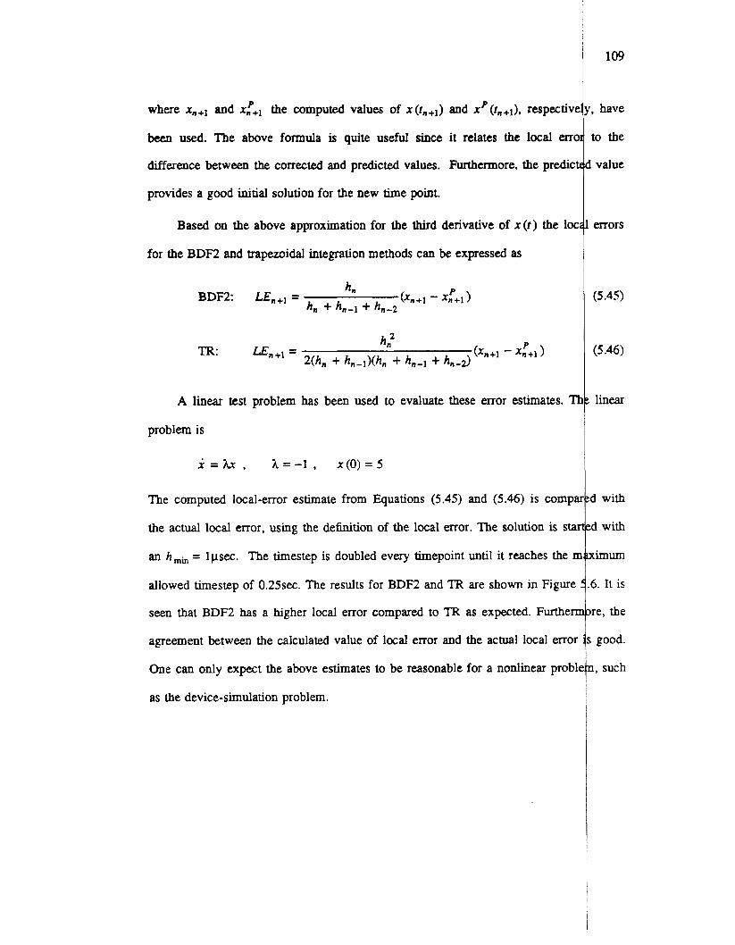
where x , + ~ and x:+] the computed values of x (r,+)) and x p (rn +]), respectivc
been used. The above formula is quite useful since it relates the local errc
difference between the corrected and predicted values. Furthemore, the predicl
provides a good initial solution for the new time point.
Based on the above approximation for the third derivative of ~ ( t ) the loc
for the BDF2 and trapezoidal integration methods can be expressed as
A linear test problem has been used to evaluate these error estimates. T
problem is
X = k , h = - l , x ( O ) = 5
The computed local-error estimate from Equations (5.45) and (5.46) is compe
the actual local error, using the definition of the local error. The solution is sta
an hmi, = Ipsec. The timestep is doubled every timepoint until it reaches the II
allowed timestep of 0.25sec. The results for BDF2 and TR are shown in Figure
seen that BDF2 has a higher local error compared to TR as expected. Furthem
agreement between the calculated value of local error and the actual local error
One can only expect the above estimates to be reasonable for a nonlinear probli
as the device-simulation problem.
109
, have
to the
value
errors
(5.45)
(5.46)
linear
d with
d with
:imLlIn
5 . It is
re, the
good.
, such
110
I
LE( 1 ) x 10
16.00
14.00
12.00
10.00
8.00
6.00
4.00
2.00
0.00 Time (sec)
0.00 2.00 4.00
Figure 5.6: Estimated and actual values of local error for the tra- pezoidal and BDF2 integration methods.
55.3. Time-Step Control in CODECS
E u c r = Er IXn+1 I + Ea
The timesteps can be controlled by considering the relative error of the allowabe
error and the actual local error.
Timesteps used during transient analysis must ensure accuracy of a s
integration scheme which is used for the solution of stiff systems. The simp
is to use a fixed timestep over the whole time interval. However, t h i s is not
for stiff problems, such as the circuit- and device-simulation problems, btxa
constants of the equations may vary by several orders of magnitude. The
be small enough to accurately resolve the fast transients. This results in
extremely large number of timepoints when computing a solution with
transients. Varying the timestep during the simulation can provide speed a
racy. Thus, fast transients would be resolved with small timesteps wh
slow transient larger timesteps are used. This section describes the time
at the device level in CODECS. The allowed timesteps are determin
error estimates derived earlier.
A solution computed at timepoint rn+l by use of an integrati
sidered to be acceptable if the local error En+1 is less than a user-s
ance, i.e.,
(5.48)
local
(5.47)
where E,,, can be expressed in terms of a relative error tolerance and an a solute
error-tolerance parameter E , and E , , respectively. These parameters are used to ontrol I the accuracy,
112
Thus, the allowable timestep for the kth-order method is given by
where
The value of r u is used to select or reject the new timestep based on an a p
analysis. For device-level equations it is appropriate t~ use a root-mean-squared L
calculating the relative error [5.23]. Thus r is calculated as
(5.50)
(5.51)
teriori
m for
(5.52)
where N is the number of equatioas.
The timestep selection criterion is now described. Consider the solution at ti$ne t,+]
which was computed using a timestep h,. If rLE e 0.9 then timestep h, is rejecled and
the solution for tn+l is attempted with a new timestep h* = h, xr, . For values of
r , 2 0.9, the timestep is considered acceptable and the new timestep is taked to be
MIN (r , x h, , 2.0 x h, , hprin, ), where hphn, is the print-time interval. At each tir$epoint
the timestep is allowed to increase by at most a factor of two and never allobed to
exceed the print-time interval. In addition to the relative error criterion a time oint is
also rejected if too many iterations are required for convergence at that timepo+t. The
timestep is rejected whenever convergence is not achieved in ten iterations and a new
solution is attempted with a timestep of h* = -
d
h n 8 ’ I
It is well known that stability results for the various integration methods ard appli-
cable only when uniform timesteps are used. Nothing can be said about the sta
an integration method when the timesteps are allowed to vary. It can only be
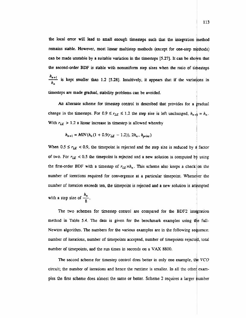
the local error will lead to small enough timesteps such that the integration
remains stable. However, most linear multistep methods (except for one-step n
can be made unstable by a suitable variation in the timesteps [5.27]. It can be shc
the second-order BDF is stable with nonuniform step sizes when the ratio of ti
is kept smaller than 1.2 [5.28]. Intuitively, it appears that if the varia hn +I
hn -
timesteps are made gradual, stability problems can be avoided.
An alternate scheme for timestep control is described that provides for a
change in the timesteps. For 0.9 I rLE S 1.2 the step size is left unchanged, h,.
With rLE > 1.2 a linear increase in timestep is allowed whereby
h,+l = MZiV(hn(l + 0.9(rU - 1.2)), 2hn, hphnt)
When 0.5 5 r u < 0.9, the timepoint is rejected and the step size is reduced by
of two. For r u < 0.5 the timepoint is rejected and a new solution is computed t
the first-order BDF with a timestep of rLExh,. This scheme also keeps a check
number of iterations required for convergence at a particular timepoint. Whem
number of iteration exceeds ten, the timepoint is rejected and a new solution is at
with a step size of -. hn 8
The two schemes for timestep control are compared for the BDF2 intl
method in Table 5.4. The data is given for the benchmark examples using t
Newton algorithm. The numbers for the various examples are in the following se
number of iterations, number of timepoints accepted, number of timepoints reject1
number of timepoints, and the run times in seconds on a VAX 8800.
The second scheme for timestep control does better in only one example, t:
circuit; the number of iterations and hence the runtime is smaller. In all the othe
ples the first scheme does almost the same or better. Scheme 2 requires a larger
113
tethod
bods)
n that
esteps
ins in
adual
= h, .
factor
using
jn the
:r the
n p t d
ration
! full-
ience:
, total
vco ZXXil-
mber
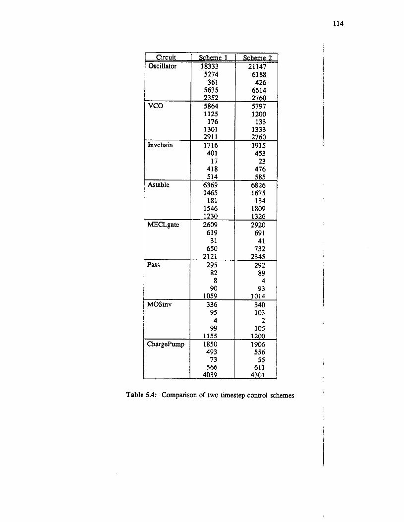
114
Circuit Oscillator
vco
Invchain
Astable
MECLgate
Pass
MOSinv
ChargePump
Scheme 1 Scheme 2 18333 21 147 5274 6188 361 426
5635 6614 2352 2760 5864 5797 1125 1200 176 133
1301 1333 291 1 2760 1716 1915 40 1 453
17 23 418 476 514 585
6369 6826 1465 1675 181 134
1546 1809 1230 1326 2609 2920 619 69 1 31 41
650 732 2121 2345 295 292 82 89
8 4 90 93
1059 1014 336 340
95 103 4 2
99 105 1155 1200 1850 1906 493 556
73 55 566 61 1
4039 4301
Table 5.4: Comparison of two timestep control schemes
of timepoints and this is due to the restrictions imposed on the timesteps. Since
scheme does not show any instability in these examples, there may be no
advantage in using a timestepcontrol strategy that is as restrictive as the second
Therefore, in CODECS, the first scheme is used for controlling the timesteps.
For the trapezoidal integration method, the two schemes are compared in Ti
The conclusions again are similar to those obtained with the BDF2 integration. '
scheme does better in almost all the examples.
Finally, the results for the BDF2 and trapezoidal methods are compared for
timestep control scheme in Table 5.6. This comparison allows an evaluation o
integration method is more suitable for use in a mixed-level circuit and device sir:
The TR integration performs remarkedly better on the Oscillator, MECLg
Pass circuits. For the other examples it performs almost similar to BDF2 or
worse than i t From this data it is clear that TR integration does not prc
significant an improvement in performance as it did for circuit simulation [5.1]. 1
number of timepoints (accepted and rejected) are smaller with the TR algorithm
number of rejected timepoints is significantly larger when compared with BDI
indicates that computational effort is wasted in determining the solution at tix
that are eventually rejected. The timepoints are rejected whenever the timestep
meet the error criterion or when convergence is not achieved in ten iterations. A
of the timepoint rejections is presented in Table 5.7, where the statistics of tir
rejected by the error criteria ( Local m o r Reject) and due to nonconvergence
Reject) are given for the BDF2 and TR integration methods. The number of i
required per timepoint are also included.
For the BDF2 method, a significant number of timepoints are rejected due
convergence only in the VCO and Astable examples. This is to be expected s
circuit waveforms have sudden transitions which result in a large change in the
115
e first
parent
heme.
e 5.5.
e first
e first
which
lator.
e and
ightly
de as
! total
ut the
This
points
1ilS to
&P
points
ancon
ations
non-
:e the
minal
116
Circuit Oscillator
vco
Invchain
Astable
MECLgate
Pass
MOSinv
Chargepump
Scheme 1 16127 349 1 705 4196 2063 5890 1003 209 1212 3000 1738 322 66 388 545 5744 1107 216 1323 1139 1966 429 55 484 1680 240 67 4 71 865 326 86 7 93
1120 1853 399 81 480 41 24
Scheme 2 16712 3939 539 4478 2103 5923 1049 186 1235 3029 1715 346 45 39 1 514 6406 1331 219 1550 1232 2138 476 53 529 1806 232 71 2 73 858 31 7 85 3 88
1108 1887 441 73 514 4396
Table 5.5: Comparison of two timestep control schemes
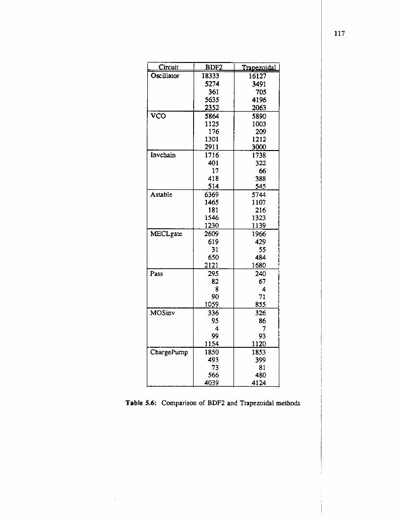
vco
lnvchain
Astable
MECLgate
Pass
MOSinv
ChargePump
BDF2 18333 5274
361 5635 2352 5864 1125 176
1301 291 1 1716 40 1
17 41 8 514
6369 1465 181
1546 1230 2609 619 31
650 2121 295 82 8
90 1059 336 95 4
99 1154 1850 493
73 566
4039
Trapezoidal 16127 3491 705
4196 2063 5890 1003 209
1212 3000 1738 322 66
388 545
5744 1107 216
1323 1139 1966 429
55 484
1680 240 67 4
71 855 3 26 86 7
93 1120 1853 399
81 480
4124
Table 5.6: Comparison of BDF2 and Trapezoidal methods
117
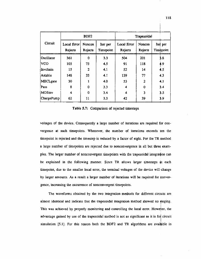
118
Noncon Rejects
Circuit 1 4 p e r Timbpoint
Oscillator vco Invchain
Astable
MECLgate Pass MOSinv Chargehrmp
201 118
14
77 2 0 3
39
Local Error Rejects
I
8.8
i . 9 4.5
1.3 4.1
a .4 3.5 3.9
361 103
15
148
30 8 4
62
BDF2
Noncon Rejects
0
73 2
33 1
0
0 11
Iter per Timepoint
3.3 4.5 4.1
4.1
4.0 3.3 3.4 3.3
1 Trapezoidal
Local Error Rejects
504 91 52
139 53 4 4
42
Table 5.7: Comparison of rejected timesteps
voltages of the device. Consequently a large number of iterations are required fDr con-
vergence at such timepoints. Whenever, the number of iterations exceeds ten the
timepoint is rejected and the timestep is reduced by a factor of eight. For the TR method
a large number of timepoints are rejected due to nonconvergence in all but thrw exam-
ples. The larger number of nonconvergent timepoints with the trapezoidal inteptlon can
be explained in the following manner. Since TR allows larger timesteps qt each
timepoint, due to the smaller local error, the terminal voltages of the device will change
by larger amounts. As a result a larger number of iterations will be required for ponver-
gence, increasing the occurrence of nonconvergent timepoints.
The waveforms obtained by the two integration methods for different circcits are
almost identical and indicate that the trapezoidal integation method showed no p i n g .
This was achieved by properly monitoring and controlling the local error. Howe+er, the
advantage gained by use of the trapezoidal method is not as significant as it is fo
simulation [5.1]. For this reason both the BDF2 and TR algorithms are avai
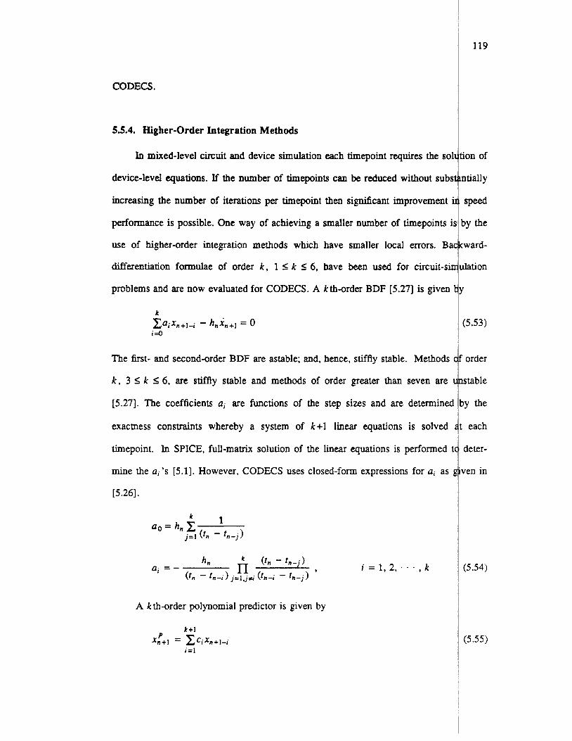
CODECS .
5.5.4. Higher-Order Integration Methods
In mixed-level circuit and device simulation each timepoint requires the sol
device-level equations. If the number of timepoints can be reduced without subs
increasing the number of iterations per timepoint then sipilkant improvement i
perfonnance is possible. One way of achieving a smaller number of timepoints ii
use of higher-order integration methods which have smaller local errors. Ba,
differentiation formulae of order k, 1 I; k I 6, have been used for circuit-sir
problems and are now evaluated for CODECS. A kth-order BDF [5.27] is given
k
i=O
The first- and second-order BDF are astable; and, hence, stiffly stable. Methods 1
k , 3 5 k I 6, are stiffly stable and methods of order greater than seven are I
[5.27]. The coefficients ai are functions of the step sizes and are determined
exactness constraints whereby a system of k + l linear equations is solved
timepoint. In SPICE, full-matrix solution of the linear equations is performed t
mine the ai's [5.1]. However, CODECS uses closed-form expressions for ai as ;
[5.26].
k
A kth-order polynomial predictor is given by
i = 1.2, . . . , k
119
ion of
ntially
speed
)y the
dation
(5.53)
order
stable
iy the
each
deter-
den in
(5.54)
(5 .55)
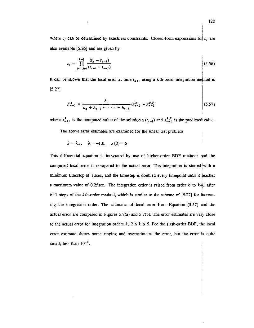
, 120
where ci can be determined by exactness constraints. Closed-form expressions fo
also available 15.261 and are given by
It can be shown that the local error at time fn+l using a kth-order integration method is
[5.27] I E
(5.57) I
where xt+l is the computed value of the solution x ( fn+ l ) and xt$ is the predicted1 value.
The above error estimates are examined for the linear test problem
x = 3tr, h=-1.0, x ( O ) = 5
This differential equation is intepted by use of higher-order BDF methods and the
computed local error is compared to the actual error. The inteption is started with a
minimum timestep of lpsec, and the timestep is doubled every timepoint until it baches
a maximum value of 0 . 2 5 ~ ~ . The integration order is raised from order k to k41 after
k+l steps of the kth-order method, which is similar to the scheme of [5.27] for $creas-
ing the integration order. The estimates of local error from Equation (5.57) dpd the
actual error are compared in Figures 5.7(a) and 5.7(b). The error estimates are verp close
to the actual error for integration orders k, 2 5 k 5 5 . For the sixth-order BDF, t4e local
error estimate shows some ringing and overestimates the error, but the error is quite
small; less than
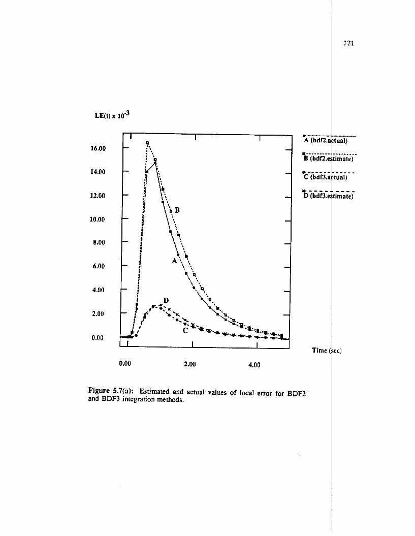
LE(t) x
16.00
14.00
12.00
10.00
8.00
6.00
4.00
2.00
0.00 I I
Time
0.00 2.00 4.00
Figure 5.7(a): Estimated and actual values of local error for BDF2 and BDF3 integration methods.
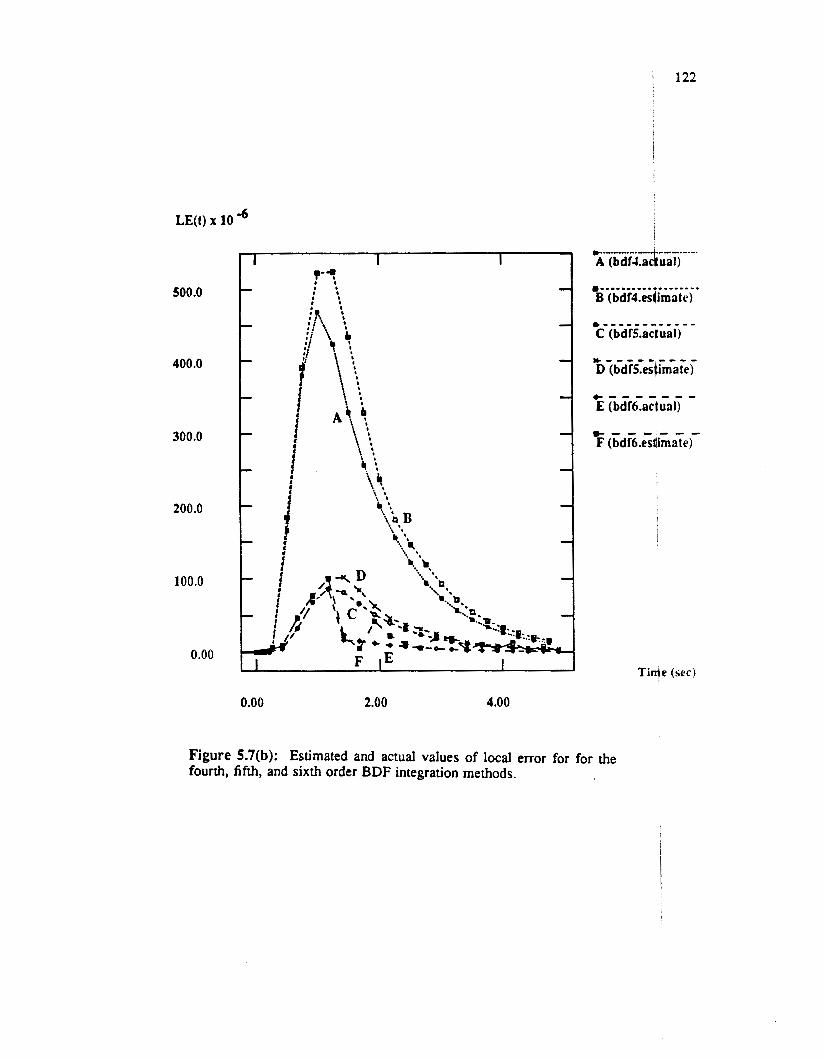
122
LE(t) x 10
500.0
400.0
300.0
200.0
100.0
0.00
0.00 2.00 4.00
*.--...- ...-.......... A (bdMaaual)
Tide (sec)
Figure 5.7(b): Estimated and actual values of local error for for the fourth, fifth, and sixth order BDF integration methods.
5.5.5. Timestep and Order Control for Higher-Order BDF
Higher-order BDF methods allow the choice of an integration order along
new timestep. Thus, both timesteps and integration order can be varied and this
done in a manner that ensures accuracy and provides an improvement in perform
method of order k is used at a particular timepoint whenever it allows the
timestep. The order-selection criterion is based on [5.27].
Assume that the solution at a particular timepoint rn+l has been computed
of a kth-order integration method, 2 5 k S 5. If the local-error criterion accc
timepoint, the local error for the (k-1)th-order method is compared to that of t
order method. If the lower-order method allows a timestep greater than that of 1
order method by a factor of orderDownFactor, then the (k-1)th-order intr
method is used for calculating the solution at the next timepoint. When ther
advantage in using the low-order method, the possibility of increasing the intl
order is evaluated. If the (k+l)th-order method allows a timestep greater than thai
kth-order method by a factor orderUpFucfor then order k+ l is selected for COI
the solution at the next timepoint. Obviously for the first-order method only an i
in order is attempted, whereas for the sixth-order method only a decrease in order
sible. The condition for changing orders is evaluated after every k + l timepoir
been computed with the kth-order integration method.
The timestepcontrol scheme is the same as that used for the second-order E
compare the performance of variable timestep, variable integration order scheme$
linear device-level problem has been solved. A transient simulation is perform1
MOSFET connected as a capacitor, the source, drain, and substrate termI
grounded and the gate voltage is ramped from +5V to -5V in 10nsec; the Mi
capacitor-voltage characteristics can be determined. In Table 5.8, the results obta
various values of the relative tolerance parameter E, for an orderUpFactor of 1.2
123
crith a
ust be
Ice. A
argest
y use
!s the
> kth-
kth-
ration
is no
ration
or the
luting
:rase
; pos-
have
F. To
L non-
on a
IS are
3-gate
Ed for
nd an
124
orderDownFuctor of unity are compared. The latter condition ensures that a low? order
will be used whenever two integration orders allow the same timestep. The noblinear
equations are solved with a relative error tolerance of E,, whereas the local-erro check 4 uses a relative error tolerance of IO&, . The data is given in the sequence: n
accepted timepoints, number of rejected timepoints, number of iterations, an
time in seconds on a VAX 8800. No statistics are given for a maximum order
the highest order that was used was 5. From Table 5.8 it is seen that for ti
tolerances the higher-order methods provide some speedup. However, going
third-order method does not provide significant improvement. For an E, =
maximum order of five results in a poorer performance compared with a max
of three. Thus, methods higher than three do not provide any sigillficant imp
performance. For looser tolerances, the second-order method is quite adequate.
As additional data, consider the data of Table 5.9 obtained by using an
orderUpFuctor of 2.0 and an orderDownFactor of unity. This choice of parsmeter
allows a higher-order method to be used only if the timestep is larger by a factor /Df two
compared with the lower-order integration method. With this choice of parametels, it is
seen that the highest order used was three. Furthermore, it does not provide an addi-
tional speedup compared with the second-order method. In conclusion, a seconq-order
method provides reasonable performance for transient analysis.
4
I
At each timepoint the numerical devices converge in a different number
tions depending on how their terminal voltages vary. Lf a device converges at a
lar operating point and its terminal voltages do not change then there is no
evaluate the device. This form of latency, called iteration-domain latency,
found to be useful in event-dnven simulation [5.29]. The latency check in
5.5.6. Iteration-Domain Latency
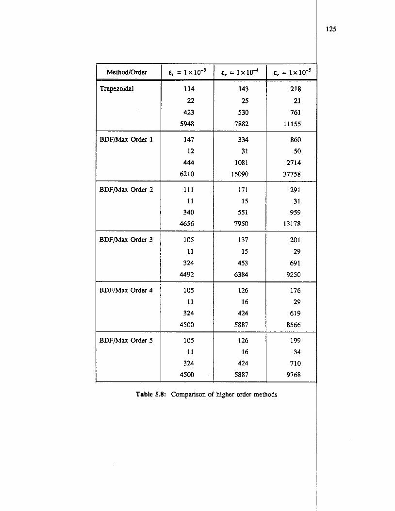
MethodJOrder
Trapezoidal
BDF/Max Order 1
BDF/Max Order 2
B D F W Order 3
BDF/Max Order 4
BDF/Max Order 5
E, = 1 x 10-~
114 22 423 5948
147 12 444 6210
111 11 340 4656
105 11 324 4492
105 11
324 4500
105 11
324 4500
E, = 1 x lo4
143 25 530 7882
334 31
1081 15090
171 15
55 1
7950
137 15 453 6384
126 16 424 5887
126 16 424 5887
~, E, = 1x10⁻⁵
218 1 21 761
11155
860 50
2714 37758
29 1 31 959
13178
201 29 69 1 9250
176 29 619 8566
199 34 710 9768
125
I
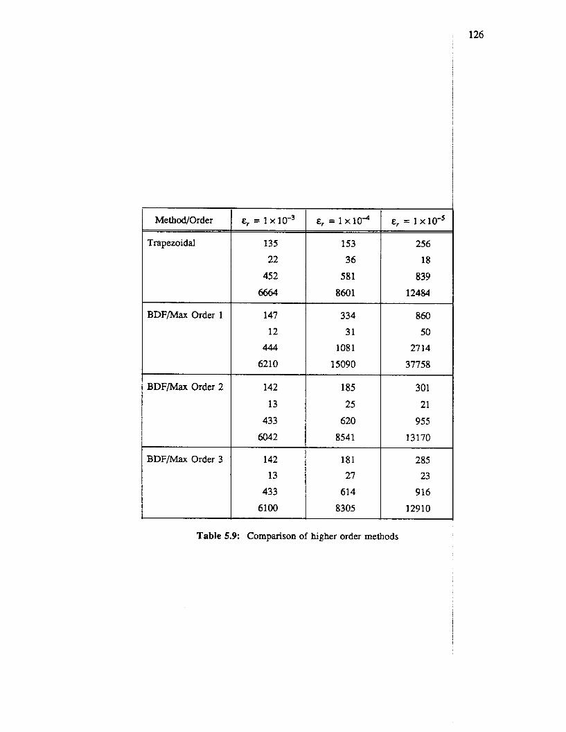
126
BDF/Max Order 1
Method/Order I E, = l X 1 0 - 3 1 E, = 1 X10⁴
6664 860 1
147 334 12 31 444 1081 6210 15090
Trapezoidal
BDF/Max Order 3
135 22 452
13 433 6042
142 181
153 36 581
~~~~
BDFNax Order 2 1 142 I 185
13 433
25 620 8541
I 6100 I 8305
E, = 1 x ~ o - ~
256 18
839 12484
860 50
2714 37758
301 21
955 13170
285 23 916
12910
Table 5.9: Comparison of higher order methods
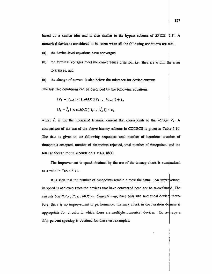
based on a similar idea and is also similar to the bypass scheme of SPICE
numerical device is considered to be latent when all the following conditions are
(a)
@)
the device-level equations have converged
the terminal voltages meet the convergence criterion, i.e., they are within 1
tolerances, and
the change of current is also below the tolerance for device currents (c)
The last two conditions can be described by the following equations.
Ivk - Vk-1 I < E,MAX(IVk I , IVk-1 I) + E,
I l k - fk I < E , M A X ( I l k I, I f k I) + Ea
where f k is the the linearized terminal current that corresponds to the voltag
comparison of the use of the above latency scheme in CODECS is given in Tal
The data is given in the following sequence: total number of iterations, nu
timepoints accepted, number of timepoints rejected, total number of timepoints,
total analysis time in seconds on a VAX 8800.
The improvement in speed obtained by the use of the latency check is sun
as a ratio in Table 5.11.
It is seen that the number of timepoints remain almost the same. An impr
in speed is achieved since the devices that have converged need not be re-evaluz
circuits Oscilluror, Puss, MOSinv, ChurgePump, have only one numerical devic
fore, there is no improvement in performance. Latency check in the iteration d
appropriate for circuits in which there are multiple numerical devices. On a
fifty-percent speedup is obtained for these test examples.
127
.1]. A
: error
: 5.10.
ber of
nd the
IariZed
rement
d. The
there-
nain is
rage a

128
With Latency Check
18333 5274 361
5635 2352 5864 1125 176
1301 291 1 1716 40 1
17 41 8 514
6369 1465 181
1546 1230 2609 619 31
650 2121 295
82 8
90
circuit
Oscillator
No latency Check 18333 5274 361
5635 2353 5865 1113 172
1285 4467 1749 40 1
17 418 908
6762 1473 177
1650 1713 2602 619 31
650 3893 296 82 8 90
vco
1059 336
Invchain
1160 3 27
Astable
MECLgate
Pass
95 4
99
MOSinv 95 4
99 1155 1239 1850 1853
566 4039 4356
Table 5.10: Statistics with and without latency check
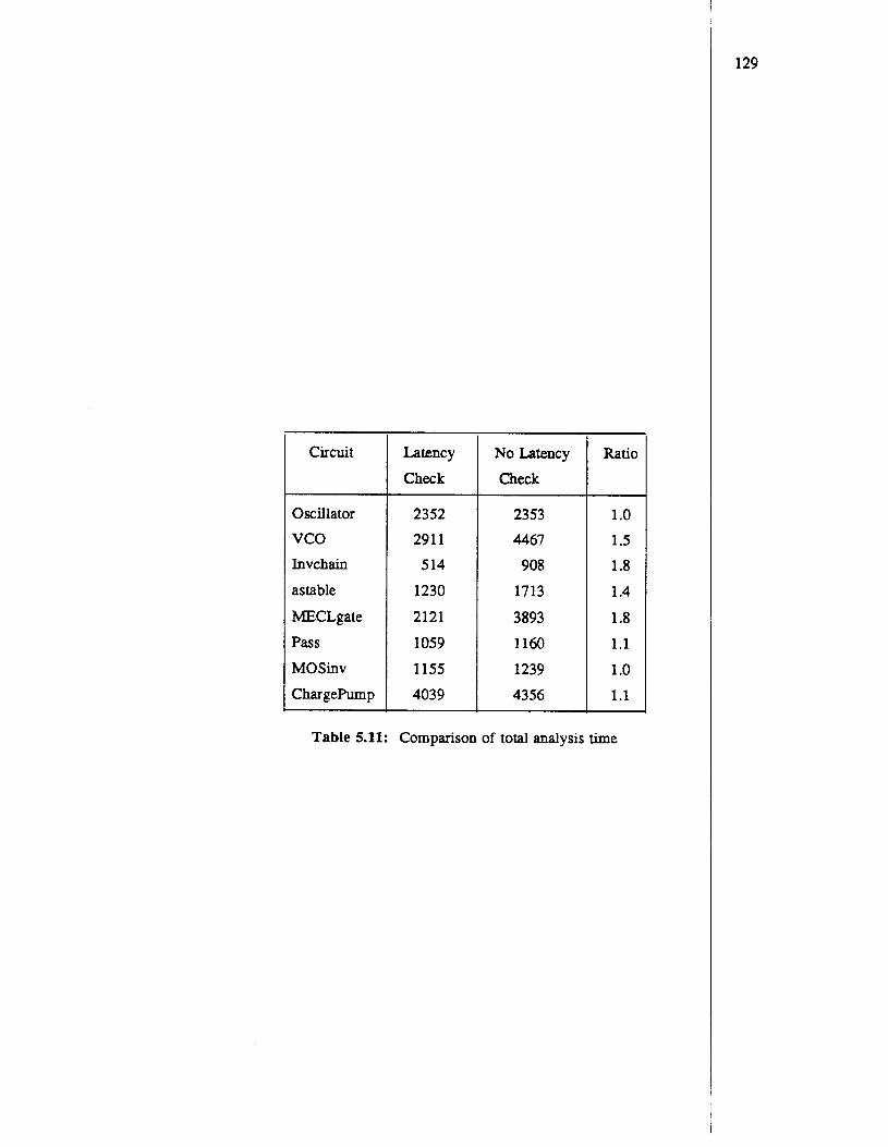
circuit I
Oscillator vco Invchain
astable
MECLgate Pass MOSinv ChargePump
I
Latency
Check
2352 291 1 514 1230 2121 1059 1155 4039
No Latency Check
2353 4467 908 1713
3893 1160 1239 4356
Ratio
1 .o 1.5 1.8 1.4
1.8 1.1 1 .o 1.1
Table 5.11: Comparison of total analysis time
130
! 5.5.7. Current-Conservation Property of BDF
In this section it is shown that the space-discretized equations consenle total
current when discretized in time by use of the backward-differentiation form+. It is
shown in [5.30] that the Grst-order BDF conserves current. Here the result is gen ralized
to the highex-order BDF. In fact, it can be shown that any linear-multistep int gration
method will possess this property.
e tl i + Current conservation is easily demonstrated for a one-dimensional diode, d can
be extended to two-dimensional devices. The device equations for grid node i loaated at
xi can be expressed as
[5 .5 8a)
(5.58~)
The total current for the interval (x i , ) is the sum of the electron current, tlbe hole
current, and the displacement current.
JT.i+Y2 = Jn.i+l12 + Jp,i+l12 + J d , i + l R
To show current conservation it suffices to show that
JT.i+1/2 = JT.i- l /2
(5.59)
(5.60)
since current will be a constant in a one-dimensional diode when the total current 11s con-
served. Recall that the displacement current is related to the electric field. In nonbalized
form
I( 5.6 1 a)
With the finitedifference scheme for space discretization, described earlier,
From Equation (5.58a) Jd,;+]n can be related to J d , i - l ~ as
Now discretizing the time derivatives by use of BDF of order k, 1 5 k 5 6,
t = fm , and evaluating J T , ; + ~ ~ ~ , one obtains
which can be simplified to
hi + hi-1 2
The term in the summation is zero, since Ni is a constant for all time points
integration method satisfies the exactness constraint, i.e., Eaj = 0. This g j=O
k
desired result; the space-discretized equations exhibit continuity of current wk
discretization is performed by the kth-order backward-differentiation formula.
5.6. Small-Signal Ac and Pole-Zero Analyses
Steady-state sinusoidal analysis at the device level was described in Ck
There it was shown that the device-level equations can be assembled in the form
[$ + Jo(o)]w(o) = b
131
.61b)
15.62)
time
15.63)
15.64)
d the
s the
time
ter 3.
(5.65)
132
aF aw
where - is the Jacobian matrix of the device-level equations at the dc operatin
and D is a diagonal matrix with diagonal entries 0, -di, and ai, correspondin$ to the
Poisson equation, the electron currentcontinuity equation, and the hole current-co tinuity
equation, respectively. Ai is the area of the region associated with grid node ii, and
i+ = w, + j w i is the vector of the small-signal internal device variables. The aboke sys- t
tem of equations can be solved by a SOR-technique as described in Chapter 3,
works well at low frequencies. At higher frequencies it can be shown that the re1
t
method will have very slow convergence. For this reason, CODECS uses
Siedel relaxation at low frequencies and switches to a direct method whenever
ation method fails to converge in five iterations. The direct method solves the
system of linear coupled equations simultaneously and always obtains the solutiob. This
process is explained in detail below.
At low frequencies, CODECS solves the decoupled system of equations obtained
by Gauss-Siedel (GS) relaxation as
(5.66a)
(5.66b)
where k is the iteration count for the relaxation method. The above decoupling bas the
advantage that - is available in its LU-factors from the dc operating point soldtion of aF aw
the device-level equations; only forward and back substitutions are required in solving
w, and wI, which makes the computations extremely efficient. As an example, b fifty-
point ac analysis of a single MOSFET circuit took 315sec with the GS method,
the direct method required 2608sec. Clearly the GS approach is more efficient
result in significant savings of CPU time, particularly so for low frequencies
circuit examples.
r
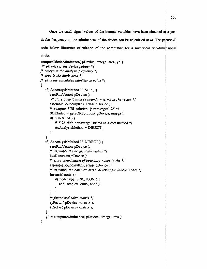
Once the small-signal values of the internal variables have been obtained I
ticular frequency a, the admittances of the device can be calculated at a. The pi
code below illustrates calculation of the admittance for a numerical one-diml
diode. computeDiodeAdmittance( pDevice, omega, area, yd ) P pDevice is the device pointer *I
P omega is the analysis frequency *I P area is the diode area */ P yd is the calculated admittance value */ t
if( AcAnalysisMethod IS SOR ) { zeroRhsVector( pDevice ); P store contribution of boundary t e r m in rhs vector */ assembleBoundaryRhsTerms( pDevice ); I* compute SOR solution. if converged OK */ SORfailed = getSORSolution( pDevice, omega ); if( SORfailed ) {
P SOR didn’t converge, switch to direct method */ AcAnalysisMethod = DIRECT;
1 1 if( AcAnalysisMethod IS DIRECT ) {
zeroRhsVector( pDevice ); I* assemble the dc jacobian matrix */ loadJacobian( pDevice ); /* store contribution of boundary nodes in rhs */ assembleBoundaryRhsTerms( pDevice ); I* assemble the complex diagonal t e r n for Silicon nodes */ foreach( node ) {
if( nodeType IS SILICON ) { addComplexTerms( node );
1 1 I* factor and solve matrix */ spFactor( pDevice->matrix ); spSolve( pDevice->matrix );
1 yd = computeAdmittance( pDevice, omega, area );
1
133
a par-
:udO-C
nsional
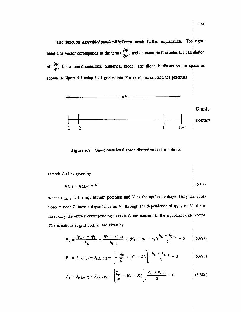
The function arsembleBoundnryRhsTerms needs further cxplanatim. The1 right-
ation T aF hand-side vector corresponds to the terns -, and an example illustrates the cal av
aF of - for a oae-dimensional numerical diode. The diode is discretized in av shown in Figure 5.8 using L+l grid points. For an ohmic contact, the potential
ohmic
1 2 L L+ 1
Figure 5.8: One-dimensional space discretization for a diode.
at node L+l is given by
W L + l = WOL+l + v
where w ~ ~ + ~ is the equilibrium potential and V is the applied voltage. Only U
contact
(5 -67)
equa-
tions at node L have a dependence on V, through the dependence of yrL+l on V/; there-
fore, only the entries corresponding to node L are nonzero in the right-hand-side/ vector.
The equations at grid node L are given by
F, = WL+I - W L - W L - WL-I h L + hL-1 = O + ( N L + P L - n L >
h L hL-1 (5.68a)
(5.68b)
(5.68~)
From these equations one obtains, i
(5.69a)
k5.69b)
(5.69~)
These derivative terms are used to assemble the right-hand-side vector. Recall, @at the
boundary terms are also assembled in the right-hand-side vector for calculating qonduc-
tances for dc and transient analyses and this is done in an identical manner.
The pole-zero analysis is simply an extension of the small-signal ac analysis tech-
nique. Instead of using a frequency o, a complex frequency s = CJ + jo is used.lSmall-
signal analysis then results in a linear system of equations that can be expressed a$
r \
(5.64) - + j D ( s ) t+ = b [E J where D(s ) is a diagonal matrix with 0, -SAi, and SAi as the diagonal entries fkx grid
node i. This system of equations is assembled, and solved by a direct method for a
given frequency s . Once fv(s ) has been obtained, the admittance Y ( s ) is calculatled in a
manner similar to the calculation of admittances described earlier for s =io. PI SOR-
solution is not attempted in this case, since the system of equations cannot be partitioned
as with s = io. These admittances are then used in the circuit-level equations to deter-
mine the poles and zeros of the circuit transfer function.
136
are critical to the performance. By estimating the sensitivity of the response to
I 5.7. Calculation of Sensitivity to Doping Profiles
all the
indicated in [5.32] where device-level sensitivities have been implemented und
ditions. Differential-sensitivity calculations are particularly useful for device
because repeated simulation of a device with different doping profiles requires
computational effort, particularly for two and three-dimensional devices. On
hand, as illustrated later in this section, sensitivities are quite inexpensive to e
provide a first-order analysis of the tradeoffs involved in device design.
The sensitivity problem is formulated as a problem for calculation of tr
sitivities. The dc sensitivities are then obtained as a special case of the transient problem
by setting the time-derivative terms to zero. Calculation of sensitivities is dorJe by a
direct-differentiation approach which has been preferred for use in circuit simurators [
5.33, 5.341.
At the device-simulation level, the system of equations that is solved can be
represented as
where w(r ) is the vector of internal variables and V (r ) are the applied terminal v ltages.
For assumed analyucal doping profiles, let u be a doping-profile parameter;
peak concentration or characteristic length for a Gaussian profile, or the concen
a uniform doping. The implicit dependence of w on u can be incorporated in
I)

137
equation, which can then be expressed as
F(W(t, u>, w(r, u>, u , V ( t ) ) = 0 ' (5.72)
To compute differential sensitivities this equation is differentiated with respect I to the
I doping-profile parameter u to obtain i
i (5.73)
I
I Since
Equation (5.73) can be rewritten as I I (5.75)
which is a system of linear differential equations in k, the sensitivities of the kternal aU variables to the parameter u . The initial condition for this system of differential equa-
tions is obtained by setting the time derivative term to zero, Le.,
The above equation also provides the dc sensitivities 1% 1.. E is available In LU-
factors from the solution of the device-level equations under dc conditions and o
ward and back substitutions are required to calculate the dc differential
When a kth-order
discretization at time r =
backward-differentiation formula (1 I k 1 2 ) is used f r time 4 ~ - - h + l r -- dw can be expressed as
at au
Substitution of the discrete approximation for the time derivative te rms in E
(5.75) results in
Assembling the terms in , one obtains
138
(5.77)
(5.78)
uation
(5.79)
(5.80)
The above equation is a system of linear equations that is solved once the devi+-level r \
equations have converged at time point t n + l . bz aF + $1 is the Jacobian u$ed for
the solution of the device-level equations at time point tn+]. Hence, it is availabld in its r .
can be obtained by forward and back substitutions, wqch are !
LU factors and
not computationally expensive.
I It should be noted that E is a diagonal matrix with diagonal entries 0, -Al, and adv
Ai corresponding to Poisson's equation and the electron and hole current-co~)tinuity
equations, respectively. Equation (5.80) requires values of the differential sensitivities I
from the previous timepoints, Le., values of [$ In and [%In-]; therefor
quantities must be stored. I
139
5.7.1. Implementation of Sensitivity Calculations
As seen from the previous derivation the sensitivities of all internal vana(b1es at
previous timepoints have to be stored; they are required for integrating the sedsitivity
differential equation. Thus, in addition to storing the values of v i , ni and p i at grild node
I
have to be stored at previous timepoints1 in the api , and - my; ani
aU aU aU i, the quantities, - -
state vector. This leads to an increase in the size of the state vector by a factor of two.
Once the right-hand-side vector for the sensitivity equation has been assemb(led the
sensitivities can be obtained by forward and back substitutions. The right-hand-side vec-
tor is made up of two terms: the first one is due to the time discretization of tha sensi-
tivity equation and the other term is due to -. The second tern requires computbg the aF au
derivatives of the equations at each grid node with respect to the doping-profile parame-
ter I(. Poisson’s equation has a direct dependence on doping through the term NA - No.
The dependence on doping enters the currentcontinuity equations through the /carrier
mobility and carrier lifetime dependencies on doping. The band-gap narrowing bnn is
also doping dependent and should be taken into account. However, for the present
implementation, this dependence has been ignored and only the doping dependent mobil-
ities and lifetimes are accounted for.
Variations in the doping also change the electrostatic potential and electron and
hole concentrations at the contact nodes. For ohmiccontact nodes the sensitivi6es can
be easily calculated from equilibrium conditions and the charge-neutrality condikion. It
can be shown for the ohmic contact that,
r5 .* a)
5.81b) I
140
and I ,(5.81c)
where N is the net doping, and n o and p o are the equilibrium electron and hole oncen-
trations at the contact. 4 1
I api , and - mVi ani Once the sensitivity equations have been solved -, - au aU aU
each grid point. From this information the sensitivities of terminal c m n
ing can be determined. Thus, for given terminal voltages one can determine the lchange
in terminal current for a change in the doping within some region of the device.
5.7.2. Sensitivity Simulation Examples
A pn-junction diode with the doping profile shown in Figure 5.9 is used as the
example. The dc sensitivity of diode current to the doping level in the lightly doped
region, No, as a function of voltage is plotted in Figure 5.10. The sensitivity plpt indi-
cates that initially the current decreases with an increase in N o , but at higher vol ges an
increase in No will result in an increase of the current. This behavior can be explained
by examining the operation of the diode under low-level and high-level-injection condi-
tions. Under low-level injection an increase in No reduces the amount of injected car-
riers and hence one can expect a reduction in the current. However, under hi@-level-
injection conditions, which occur at higher voltages, the current increases
increase in No ; the current roll-off occurs at a higher voltage. In Figure 5.10 e also
shown the sensitivities of diode current to No obtained by use of repeated sim ations
for 1%, 108, and 100% variations in the doping level. The ageement with the
the 10% deviations is extremely good, showing the accuracy of the sensitivity
tions. The 100% deviations show a trend similar to that obtained by the diff
tii
Tith an
b
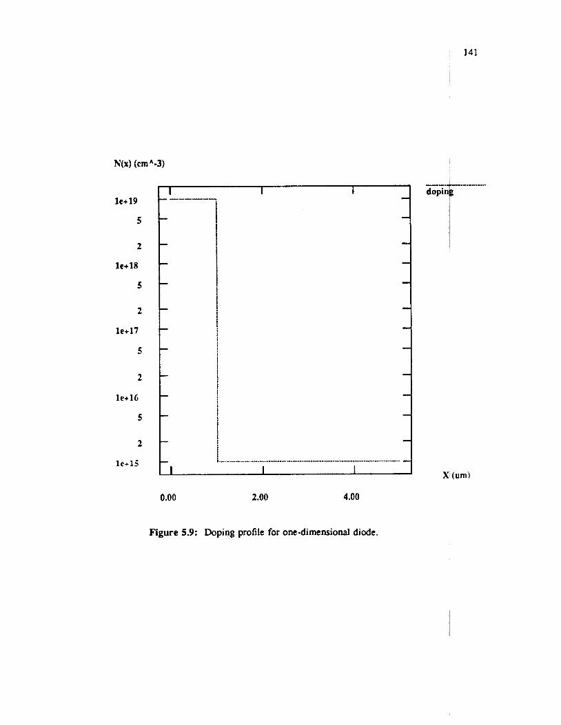
141
I I I - --- --I - - -
N(x) (cm A-3)
- - - - c
- - - - - -
- - - .................................................................................................. -
I I I
le+19
5
2
le+18
5
2
le+17
5
2
l e + l 6
5
2
le+15
0.00 2.00 4.00
Figure 5.9: Doping profile for one-dimensional diode.
-I-*
dopir
X (urn)
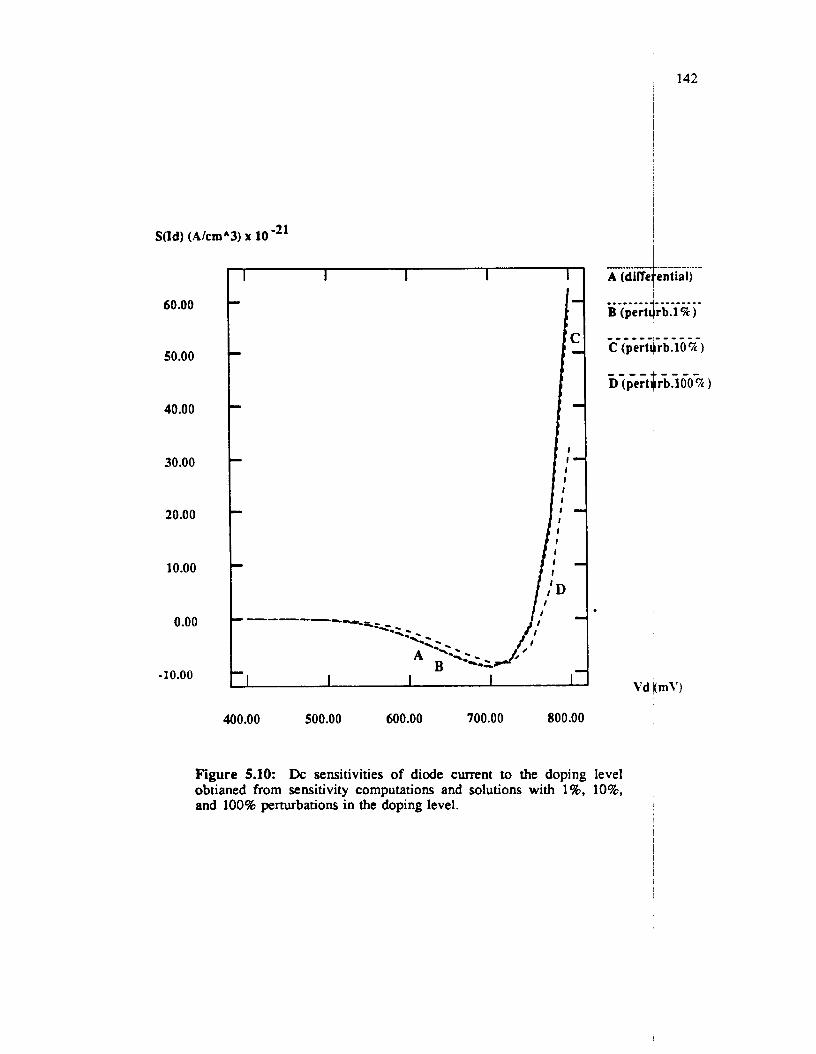
142
Sod) (A/cmA3) x
I I I I
60.00
50.00
40.00
30.00
20.00
10.00
0.00
-10.00
400.00 500.00 600.00 700.00 800.00
I -.I.-- ...-.. I ......... A (dilfefential)
I
Figure 5.10: Dc sensitivities of diode current to the doping level obtianed from sensitivity computations and solutions with 1%. lo%, and 100% penurbations in the doping level.
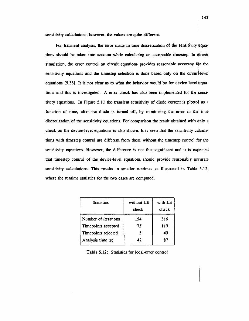
143
sensitivity calculations; however, the values are quite different.
For transient analysis, the error made in time discretization -f the sensitivity iequa-
tions should be taken into account while calculating an acceptable timestep. In eircuit
simulation, the error control on circuit equations provides reasonable accuracy f$r the
sensitivity equations and the timestep selection is done based only on the circuid-level
equations (5.331. It is not clear as to what the behavior would be for device-level equa-
tions and t h i s is investigated. A error check has also been implemented for the 5ensi-
tivity equations. In Figure 5.11 the transient sensitivity of diode current is plotted as a
function of time, after the diode is turned off, by monitoring the error in the time
discretization of the sensitivity equations. For comparison the result obtained with only a
check on the device-level equations is also shown. It is seen that the sensitivity cdcula-
tions with timestep control are different from those without the timestep control fbr the
sensitivity equations. However, the difference is not that significant and it is expected
that timestep control of the device-level equations should provide reasonably awurate
sensitivity calculations. This results in smaller runtimes as illustrated in Table 5.12,
where the runtime statistics for the two cases are compared.
Statistics
Number of iterations Timepoints accepted Timepoints rejected Analysis time (s)
without LE check
154
75
3
42
Table 5.12: Statistics for local-err
with LE check
316
119
40
87
r control
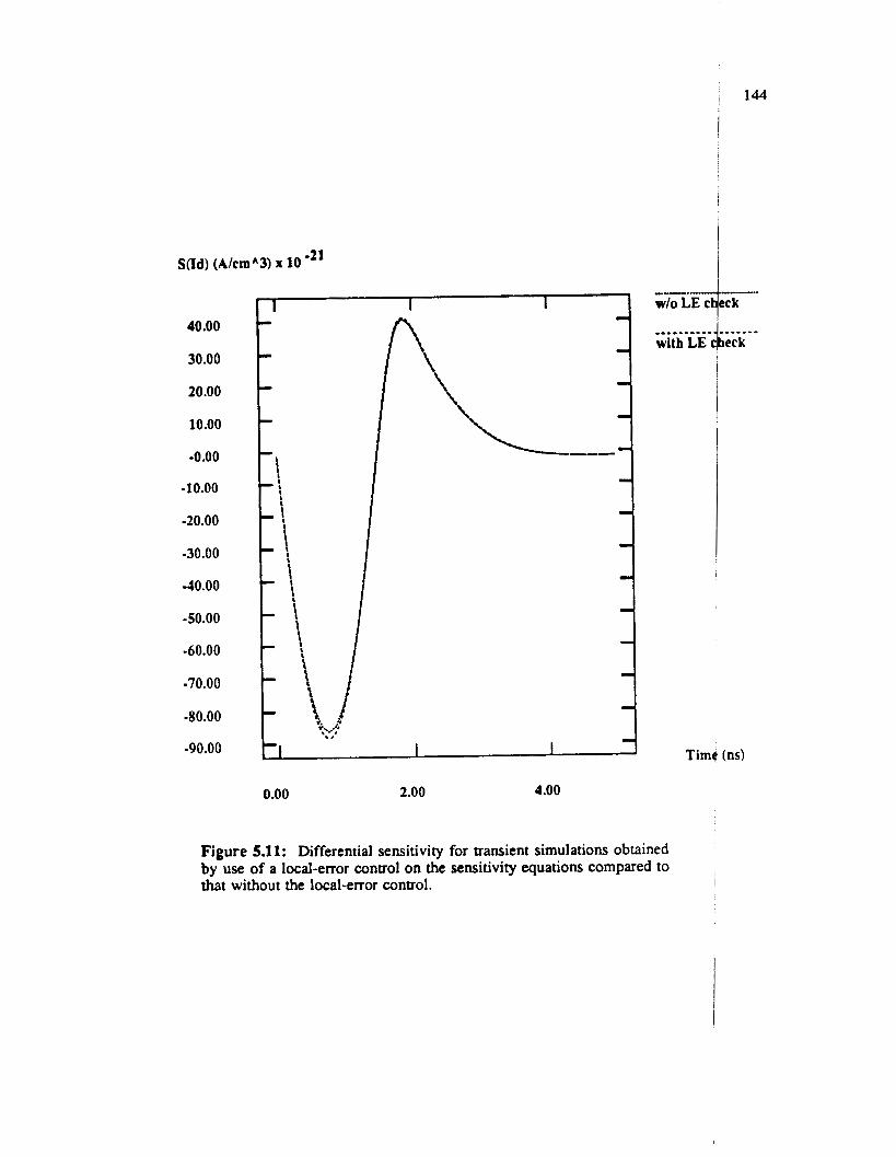
Sod) (A/cmA3) x 10 -21
40.00
30.00
20.00
10.00
-0.00
-10.00
-20.00
-30.00
-40.00
-50.00
-60.00
-70.00
-80.00
-90.00
0.00 2.00 4.00
_"...........I
wlo LE cl
with LE ---..-----
Figure 5.1 1 : Differential sensitivity for transient simulations obtained by use of a local-error control on the sensitivity equations compared to that without the local-error control.
144
.---.... eck
beck - - - - - - -
Tim4 (ns)

145
Finally, a comparison is ma& with the sensitivities calculated by use of rt*ated
simulations with 1 8 , 108, and 100% variations in the doping profiles in Figurt'5.12.
Good agreement is achieved with the 1% and 10% variation results. The 100% vadiation
result differs by about 50% from the differential-sensitivity calculation.
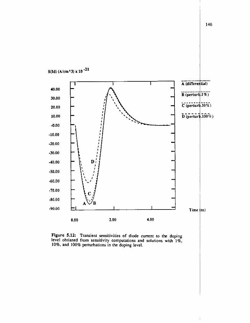
SUd) (A/cmA3) x 10 -21
40.00
30.00
20.00
10.00
-0.00
-10.00
-20.00
-30.00
-40.00
-50.00
-60.00
-70.00
-80.00
-90.00
0.00 2.00 4.00
Figure 5.12: Transient sensitivities of diode current to the doping level obtianed from sensitivity computations and solutions with I%, 108, and 100% perturbations in the doping level.
147
CHAPTER 6
CODECS Design Considerations
6.1. Introduction
An initial prototype of CODECS was implemented in Lisp using object-odented
programming. The Lisp programming language was used because of enhanced software
productivity. Furthermore, object-oriented programming allowed easy coupling between
the circuit and device simulators. Previous experience with Lispbased circuit simdlation
r6.1-6.31 indicated that there would not be a significant performance penalty on a Lisp
machine.
Consequently, a one- and two-dimensional device-simulation capability was
developed in Lisp. Object-oriented programming provides a simple interface betwedn the
device simulator and the circuit simulator. The runtime performance of the mixedblevel
circuit and device simulator is extremely poor, even on a Symbolics 3600 Lisp machine
[6.4], as illustrated in this chapter. Benchmark examples are used to evaluate the^ run-
time performance. Detailed profiling of one- and two-dimensional simulation exagnples
is provided to identij. the bottlenecks in the program. It is shown that adequate firfor-
,
mance cannot be achieved on the Lisp machine.
As a result of the above study, a new version of CODECS has been developed in
the C programming language. A new one- and two-dimensional device-simulation /capa-
bility has been written in C. SPICE3 [6.5] has been incorporated for the ci cuit-
simulation capability and for analytical models of semiconductor devices. A comp rison i
is made between the runtime performances of the Lisp and C-based versicns
CODECS. The C-based version has a significantly improved performance,
for two-dimensional simulation examples.
6.2. Lisp-based implementation - CODECSlisp
A prototype of CODECS was developed using objectsriented programmng
Lisp. The program is written in Zetalisp; objectsriented programming is
through the Flavors system [6.6]. The choices that led to the prototype being
in Lisp were: high software productivity, rapid prototyping, availability of bject-
oriented programming, and adequate performance for circuit simulation on the Sy bolics
3600 Lisp machine [a. 1-6.31.
The two main components of a mixed-level circuit and device simulation e iron-
ment are a circuit sirnulator and a device simulator. For the circuit-simulation com nent
CODECSlisp makes use of BIASlisp, an object-oriented circuit simulator [6.3]. new i
' 148
of
partitxlarly
in
avidable
dev:loped
one- and two-dimensional device simulation capability DSIM has been developed i Lisp
using object-oriented programming. The features of CODECSlisp, the choice of o jects,
and the coupling between BIASlisp and DSIM are described in [6.7]. t
6.2.1. Runtime Performance
This section examines the runtime performance of CODECSlisp for
analysis using one- and two-dimensional numerical models. Detailed
The first set of examples make use of one-dimensional numerical
lar transistors and are the Invchain and VCO examples introduced in
for transient analysis of these two circuits are presented in Table 6.1
vided to identify the portions where the program spends most of its time.
3600 Lisp machine without hardware floating-point support.
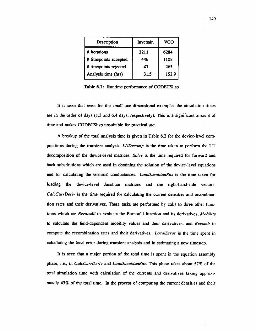
149
I Description I Invchain vco ~~~~ ~~~ ~~ ~~
221 1
446 1 :ii 1 # iterations
# timepoints accepted
# timepoints rejected 43
Analysis time (hn) 31.5 152.9
Description Invchain
# iterations 221 1
# timepoints accepted 446
# timepoints rejected 43
Analysis time (hn) 31.5
VCO
6284
1108
265
152.9
Table 6.1: Runtime performance of CODECSlisp
It is seen that even for the small one-dimensional examples the simulation times
are in the order of days (1.3 and 6.4 days, respectively). This is a significant amo nt of
time and makes CODECSlisp unsuitable for practical use. Y A breakup of the total analysis time is given in Table 6.2 for the device-level com-
putations during the transient analysis. LUDecomp is the time taken to perform the LU
decomposition of the device-level matrices. Solve is the time required for fonvartl and
back substitutions which are used in obtaining the solution of the device-level equations
and for calculating the terminal conductances. L0CrcilacobianRh.s is the time taken for
loading the device-level Jacobian matrices and the right-hand-side vqctors.
CulcCurrDeriv is the time required for calculating the current densities and reconhbina-
tion rates and their derivatives. These tasks are performed by calls to three other func-
tions which are Bernoulli to evaluate the Bernoulli function and its derivatives, M biliry
to calculate the field-dependent mobility values and their derivatives, and Reco b to
compute the recombination rates and their derivatives. LocalError is the time s t nt in
calculating the local error during transient analysis and in estimating a new timestep.
I
It is seen that a major portion of the total time is spent in the equation assembly
phase, i.e., in CalcCurrDeriv and LodacobianRhs. This phase takes about 57%
total simulation time with calculation of the currents and derivatives taking
mately 43% of the total time. In the process of computing the current densities
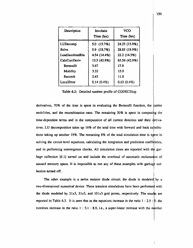
Description Invchain
Time (hrs)
LUDecomp
Solve LoadJacobianRhs CalccUrrDeriv
Bernoulli Mobility Recomb
LocalError
Table 6.2: Detailed runtime profile of CODECSlisp
5.0 (15.7%)
5.9 (18.7%)
4.54 (14.4%)
13.5 (42.9%)
3.67
3.32
2.43
0.14 (0.4%)
vco Time (hrs)
24.25 (15.9%)
28.85 (1 8.9%)
22.2 (14.5%)
65.56 (42.9%)
17.8
15.9
11.8
0.63 (0.4%)
derivatives, 70% of the time is spent in evaluating the Bernoulli function, the
mobilities, and the recombination rates. The remaining 30% is spent in comput
time-dependent terms and in the computation of all current densities and their
tives. LU decomposition takes up 16% of the total time with forward and back SI
tions taking up another 19%. The remaining 8% of the total simulation time is s:
solving the circuit-level equations, calculating the integration and prediction coeff
and in performing convergence checks. All simulation times are reported with tl
bage collection [6.1] turned on and include the overhead of automatic reclama
unused memory space. It is impossible to run any of these examples with garba,
lection turned off.
The other example is a series resistor diode circuit; the diode is modelei
two-dimensional numerical device. Three transient simulations have been performc
the diode modeled by 21x3, 51x3, and 101x3 grid points, respectively. The res1
reported in Table 6.3. It is seen that as the equations increase in the ratio 1 : 2.5
runtimes increase in the ratio 1 : 3.1 : 8.9, i.e., a super-linear increase with the I
150
anier
:riva-
IStitU-
:nt in
ients,
! gar-
3n of
! col-
by a
with
s are
5 , the
mber
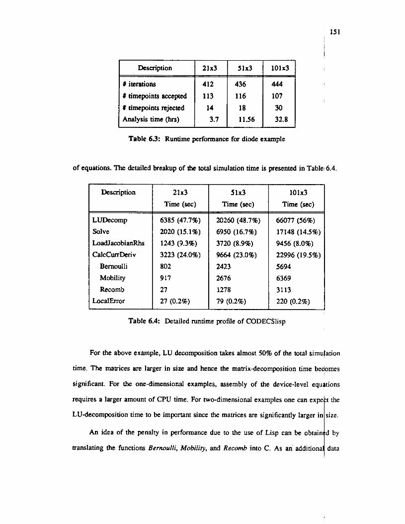
15 1
Description
# iterations
# timepoints accepted
# timepoints rejected Analysis time (hrs)
21x3 51x3 101x3
412 436 444 113 116 107
14 18 30
3.7 11.56 32.8
Table 63: Runtime performance for diode example
of equations. The detailed breakup of the total simulation time is presented in Tablei 6.4.
Description 21x3
Time (sec) ~~
LUDecomp Solve LoadJacobianRhs CalcCurrDeriv
Bernoulli Mobility
Recomb LocalError
6385 (47.7%)
2020 (15.1%)
1243 (9.3%)
3223 (24.0%)
802
917
27
27 (0.2%)
51x3
Time (sec)
20260 (48.7%)
6950 (16.7%)
3720 (8.9%)
9664 (23.0%)
2423
2676
1278
79 (0.2%)
101x3
Time (sec)
66077 (56%)
17148 (14.5%)
9456 (8.0%)
22996 (1 9.5%)
5694
6369
31 13
220 (0.2%)
Table 6.4: Detailed runtime profile of CODECSlisp
For the above example, LU decomposition takes almost 50% of the total simu[ation
time. The maaices are larger in size and hence the matrix-decomposition time beqomes
significant. For the one-dimensional examples, assembly of the device-level equations
requires a larger amount of CPU time. For two-dimensional examples one can expe t the
LUdecomposition time to be important since the matrices are significantly larger in size.
An idea of the penalty in performance due to the use of Lisp can be obtain d by
data translating the functions Bernoulli, Mobiliry, and Recomb into C. As an addition i
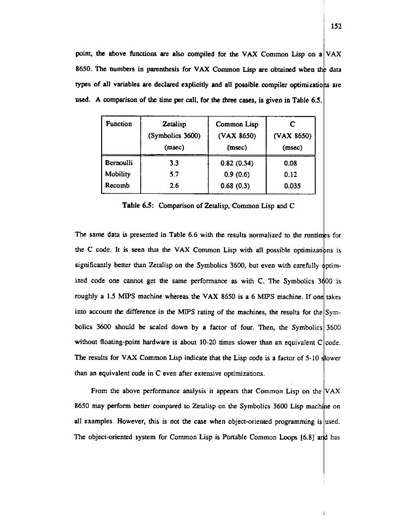
point, the above functions are also compiled for the VAX Common Lisp on a
Zetalisp (Symbolics 3600)
8650. The numbers in parenthesis for VAX Common Lisp are obtained when tl
types of all variables are declared explicitly and all possible compiler optimizatic
used. A comparison of the time per call, for the three cases, is given in Table 6.5
Common Lisp
(VAX 8650) (m=c)
Function
Bemulli Mobility
Tab1
3.3 5.7 2.6
0.82 (0.34) 0.9 (0.6) 0.68 (0.3)
6.5: Comparison of Zetalisp, Common I
C
(VAX 8650) (m=4
0.08 0.12 0.035
isp and C
The same data is presented in Table 6.6 with the results normalized to the runtin
the C code. It is seen that the VAX Common Lisp with all possible optimizat
significantly better than Zetalisp on the Symbolics 3600, but even with carefully
ized code one cannot get the same performance as with C. The Symbolics 3
roughly a 1.5 MIPS machine whereas the VAX 8650 is a 6 MIPS machine. If on1
into a m u n t the difference in the MIPS rating of the machines, the results for thc
bolics 3600 should be scaled down by a factor of four. Then, the Symbolic!
without floating-point hardware is about 10-20 times slower than an equivalent C
The results for VAX Common Lisp indicate that the Lisp code is a factor of 5-10
than an equivalent code in C even after extensive optimizations.
From the above performance analysis it appears that Common Lisp on the
8650 may perform better compared to Zetalisp on the Symbolics 3600 Lisp mach
all examples. However, this is not the case when object-oriented programming is
The object-oriented system for Common Lisp is Portable Common Loops [6.8] a
152
VAX
data
IS are
:s for
Ins is
ptim-
30 is
takes
Sym-
3600
code.
ower
VAX
le on
used.
1 has
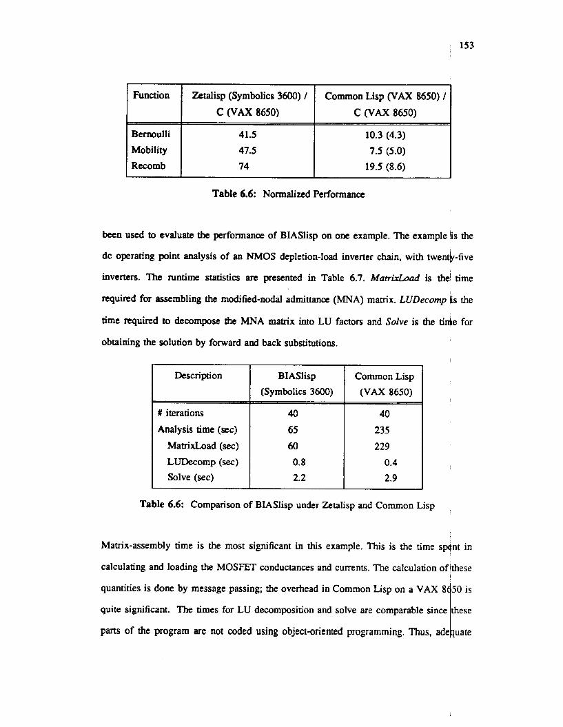
153
Function
Bernoulli Mobility Recomb
Zetalisp (Symbolics 3600) / C (VAX 8650)
Common Lisp (VAX 8650) / C (VAX 8650)
41.5 10.3 (4.3)
47.5 7.5 (5.0)
74 19.5 (8.6)
Table 6.6: Normalized Performance
been used to evaluate the performance of BIASlisp on one example. The example lis the
dc operating point analysis of an NMOS depletion-load inverter chain, with twen$-five
inverters. The runtime statistics are presented in Table 6.7. MurrXoud is the' time
required for assembling the modified-nodal admittance (MNA) matrix. LUDecomp Es the
time required to decompose the M N A matrix into LU factors and Solve is the tide for
Description
obtaining the solution by forward and back substitutions.
Common Lisp 1 (VAX 8650)
BIASlisp (Symbolics 3600)
# iterations 40 Analysis time (sec) 65
Matrimad (sec) 60
40
235 229
Table 6.6: Comparison of BIASlisp under Zetalisp and Common Lisp
LUDecomp (sec)
Solve (sec)
Matrix-assembly time is the most significant in this example. This is the time sptpt in
calculating and loading the MOSET conductances and currents. The calculation of /these
0.8 0.4
2.2 2.9
quantities is done by message passing; the overhead in Common Lisp on a VAX 8
quite significant. The times for LU decomposition and solve are comparable
parts of the program are not coded using object-oriented programming.
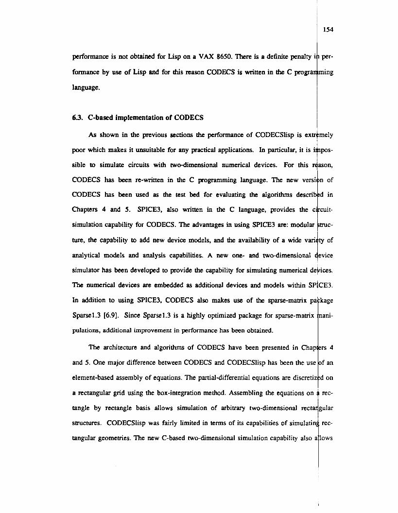
performance is not obtained for Lisp on a VAX 8650. There is a definite penalty i
formance by use of Lisp and for this reason CODECS is written in the C prograr
language.
63. C-based implementation of CODECS
As shown in the previous sections the performance of CODECSlisp is exa
poor which makes it unsuitable for any practical applications. In particular, it is i
sible to simulate circuits with two-dimensional numerical devices. For this n
CODECS has been re-written in the C programming language. The new versi
CODECS has been used as the test bed for evaluating the algorithms descrit
Chapters 4 and 5. SPICE3, also written in the C language, provides the c
simulation capability for CODECS. The advantages in using SPICE3 am modular
ture, the capability to add new device models, and the availability of a wide vari
andytical models and analysis capabilities. A new one- and two-dimensional I
simulator has been developed to provide the capability for simulating numerical dc
The numerical devices are embedded as additional devices and models within SF
In addition to using SPICE3, CODECS also makes use of the sparse-matrix pi
Sparse1.3 [6.9]. Since Sparse1.3 is a highly optimized package for sparse-matrix
pulations, additional improvement in performance has been obtained.
The architecture and algorithms of CODECS have been presented in Char
and 5. One major difference between CODECS and CODECSlisp has been the use
element-based assembly of equations. The partial-differential equations are discreti;
a rectangular grid using the box-integration method. Assembling the equations on
tangle by rectangle basis allows simulation of arbitrary two-dimensional recta
stn~ctures. CODECSlisp was fairly limited in terms of its capabilities of simulatin
tangular geometries. The new C-based two-dimensional simulation capability also :
154
per-
ning
mely
I p s -
tson,
n of
d in
cuit-
truC-
7 of
:vice
ices.
3E3.
kage
iani-
!rs 4
I f an
d on
rec-
gular
rec-
lows
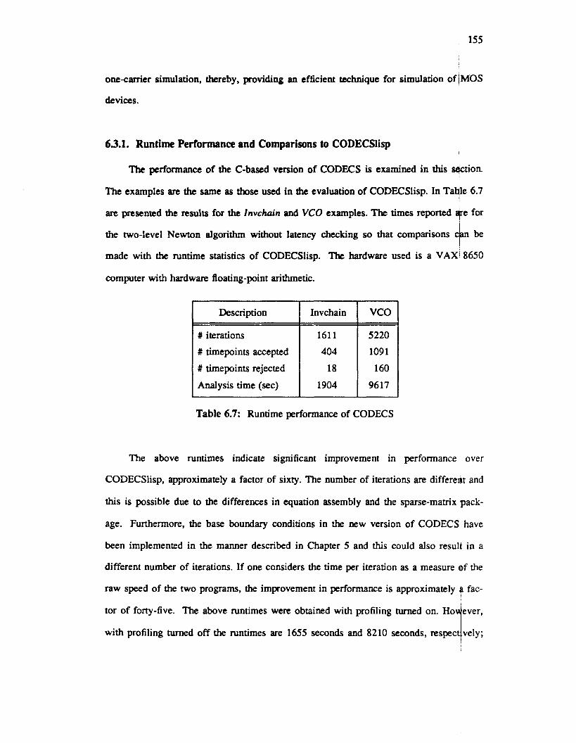
155
Description
# iterations # timepoints accepted
# timepoints rejected
Analysis time (sec)
one-carrier simulation, thereby, providing an efficient technique for simulation of IMOS
devices.
Invchain
161 1
404
18
1904
63.1. Runtime Performance and Comparisons to CODECSlisp
The performance of the C-based version of CODECS is examined in this +tion.
The examples are the same as those used in the evaluation of CODECSlisp. In Tavle 6.7
are presented the results for the Invchain and VCO examples. The times reported +e for
the two-level Newton algorithm without latency checking so that comparisons be
made with the runtime statistics of CODECSlisp. The hardware used is a VAXI 8650 +
computer with hardware floating-point arithmetic.
vco 5220
1091
160
9617
Table 6.7: Runtime performance of CODECS
The above runtimes indicate significant improvement in performance over
CODECSlisp, approximately a factor of sixty. The number of iterations are differedt and
this is possible due to the differences in equation assembly and the sparse-matrix pack-
age. Furthermore, the base boundary conditions in the new version of CODECSI have
been implemented in the manner described in Chapter 5 and this could also result in a
different number of iterations. If one considers the time per iteration as a measure of the
raw speed of the two programs, the improvement in performance is approximately B fac-
tor of forty-five. The above runtimes were obtained with profiling turned on. Ho ever,
with profiling turned off the runtimes are 1655 seconds and 8210 seconds, respect vely; 1
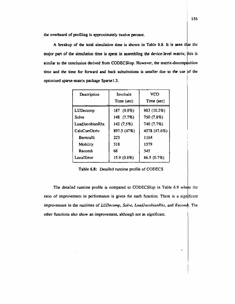
the overheard of profiling is approximately twelve percent.
A breakup of the total simulation time is shown in Table 6.8. It is seen tl
major part of the simulation time is spent in assembling the device-level matrix;
similar to the conclusion derived from CODECSlisp. However, the matrixdecomp
time and the time for forward and back substitutions is smaller due to the use
optimized sparse-matrix package Sparse 1.3.
Description
LUDecomp Solve
LoadJacobianRhs
CalCCurrDeriV Bernoulli Mobility Recomb
LocalError
Invchain
Time (sec)
187 (9.8%)
148 (7.7%)
142 (7.5%)
897.5 (47%)
223 318
68
15.9 (0.8%)
vco Time (sec)
983 (10.2%)
750 (7.8%)
740 (7.7%)
4578 (47.6%)
1164
1579
345
66.5 (0.7%)
Table 6.8: Detailed runtime profile of CODECS
The detailed runtime profile is compared to CODECSlisp in Table 6.9 whl
ratio of improvement in performance is given for each function There is a sigi
improvement in the runtimes of LUDecomp, Solve, LoodlacobianRhs, and Recom
other functions also show an improvement, although not as significant.
156
at the
his is
sition
)f the
re the
ficant
1. The
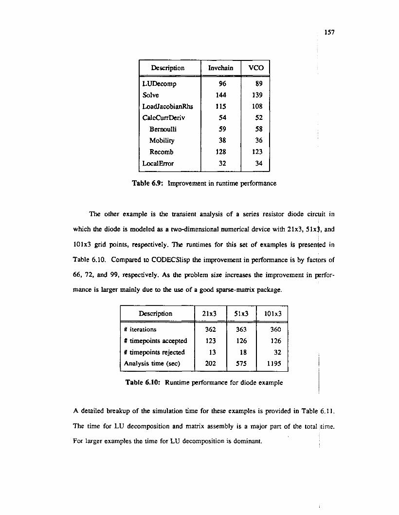
157
Description
# iterations
# timepoints accepted
# timepoints rejected Analysis time (sec)
Invchain I vco
21x3 51x3 101x3
362 363 360 123 126 126
13 18 32 202 575 1195
I Description
LUDecomp
Solve LoadJacobianRhs CalcCurrDeriv
Bernoulli Mobility
Recomb LocalError
96 144
115 54 59 38
128
32
89
139 108 52 58 36
123
34
Table 6.9: Improvement in runtime performance
The other example is the transient analysis of a series resistor diode circuit in
which the diode is modeled as a two-dimensional numerical device with 2Ix3,51x$, and
101x3 grid points, respectively. The runtimes for this set of examples is presented in
Table 6.10. Compared to CODECSlisp the improvement in performance is by factors of
66, 72, and 99, respectively. As the problem size increases the improvement in prfor-
mance is larger mainly due to the use of a good sparse-matrix package.
Table 6.10: Runtime performance for diode example
A detailed breakup of the simulation time for these examples is provided in Table 6.1 1.
The time for LU decomposition and matrix assembly is a major part of the total time.
For larger examples the time for LU decomposition is dominant. I
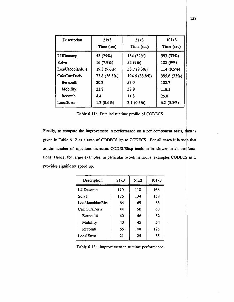
Description
LUDecomp
Solve
LoadJacobianRhs CalcCurrDeriv
Bernoulli
Mobility
Recomb LocalError
21x3 ~ Time(sec)
' 58 (29%) 16 (7.9%) 19.3 (9.6%) 73.8 (36.5%) 20.3 22.8 4.4 1.3 (0.6%)
5 1x3 Time (sec)
184 (32%) 52 (9%) 53.7 (9.3%) 194.6 (33.8%) 53.0 58.9 11.8 3,l (0.5%)
101x3 Time (sec)
393 (33%) 108 (9%) 114 (9.5%) 395.6 (33%) 108.7 118.3 25 .o 6.2 (0.5%)
Table 6.11: Detailed runtime profile of CODECS
Finally, to compare the improvement in performance on a per component basis,
given in Table 6.12 as a ratio of CODECSlisp to CODECS. For all cases it is SI
as the number of equations increases CODECSlisp tends to be slower in all tt
tions. Hence, for larger examples, in particular two-dimensional examples CODE(
provides significant speed up.
Description
LUDecomp Solve LoadJacobianRhs CalCCurrDeriV
Bernoulli Mobility
Recomb LocalError
21x3
110 126 64 44
40 40 66 21
51x3
110 134 69 50 46 45 108 25
101x3
168 159 83 60 52 54 125 35
Table 6.12: Improvement in runtime performance
158
ita is
I that
Func-
in C
CHAPTER 7
159
Comparison of Analytical and Numerical Models
7.1. Introduction
In Chapter 2 it was indicated that analytical models are inadequate under qertain
regimes of device operation. This problem is addressed in detail in the present cbapter
such that the tradeoffs between accuracy and speed performance can be made. +vera1
one- and two-dimensional examples are used and the emphasis is on transieqt and
small-signal ac response since the deficiencies of analytical models show up signifitxntly
in these analyses. The benchmark circuits that have been used in the experimeq are
also described.
The starting point for all comparisons is a set of model parameters for the M y t i -
cal SPICE model that gives a good agreement in the dc characteristics of the nuwerical
and analytical models. It is shown for both bipolar and MOS examples that even qough
the agreement between dc characteristics is good and the charge-storage effects are
modeled as accurately as possible, the dynamic response can be significantly different.
The masons for these differences am examined and provide a guideline as to iwhen
numerical models must be used.
A comparison is made in the runtime performance of the analytical and nurqerical
models. Analytical models are naturally faster in performance but do not always
accurate results. The comparison only indicates the differences in runtime
between analytical and numerical models. This then motivates the use of a
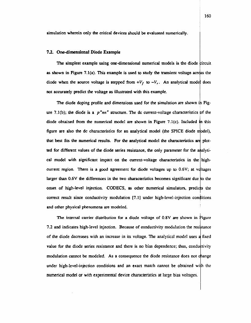
simulation wherein only the critical devices should be evaluated numerically.
7.2. One-dimensional Diode Example
The simplest example using orredimensional numerical models is the diode
as shown in Figure 7.l(a). This example is used to study the transient voltage am
diode when the source voltage is stepped from +VI to -Vr. An analytical mod6
not accurately predict the voltage as illustrated with this example.
The diode doping profile and dimensions used for the simulation are shown :
we 7.l(b); the diode is a p+nn+ structure. The dc current-voltage characteristics
diode obtained from the numerical model are shown in Figure 7.l(c). Included
figure are also the dc characteristics for an analytical model (the SPICE diode D
that best fits the numerical results. For the analytical model the characteristics ar
ted for different values of the diode series resistance, the only parameter for the a
cal model with significant impact on the went-voltage characteristics in the
current region. There is a good agreement for diode voltages up to 0.6V; at V I
larger than 0.6V the differences in the two characteristics becomes significant due
onset of high-level injection. CODECS, as other numerical simulators, predic
correct result since conductivity modulation [7.1] under high-level-injection con
and other physical phenomena are modeled.
The internal carrier dismbution for a diode voltage of 0.8V are shown in
7.2 and indicates high-level injection. Because of conductivity modulation the res
of the diode decreases with an increase in its voltage. The analytical model uses
value for the diode series resistance and there is no bias dependence; thus, condt
modulation cannot be modeled. As a consequence the diode resistance does not I
under high-level-injection conditions and an exact match cannot be obtained w
numerical model or with experimental device characteristics at large bias voltages.
160
ircuit
,s the
does
Fig-
If the
I this
)del),
plot-
alyti-
high-
tages
o the
5 the
itions
igure
tance
fixed
tivity
iange
5 the
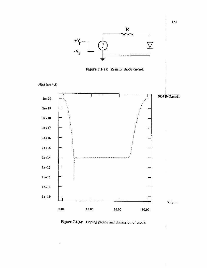
R
Figure 7.l(a): Resistor d i d circuit.
le+20
le+19
le+18
le+17
le+16
le+15
le+14
le+13
l e + l 2
le+ll
le+lO
I I I ...- - ..
.......... . DOP:
161
....... ... ..... .. . . . NG.mod 1
0.00 10.00 20.00 30.00
Figure 7.l(b): Doping profile and dimension of diode.
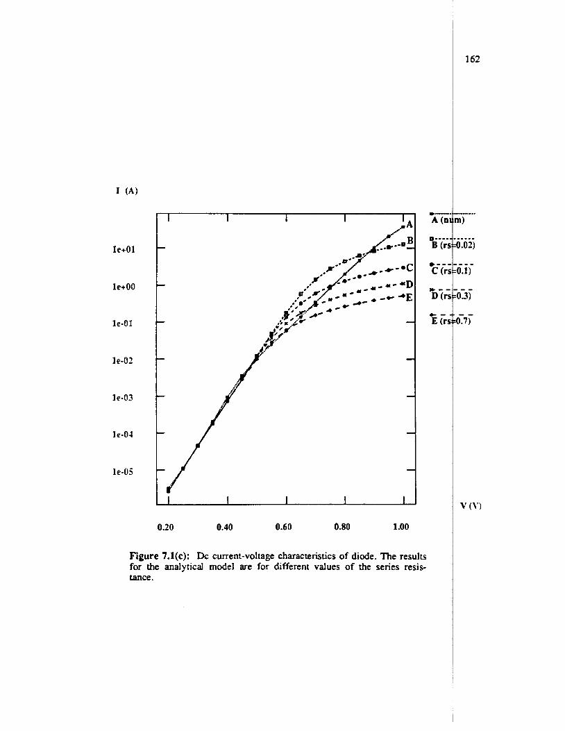
le+01
le+00
le-01
le-02
le-03
1 e-04
le-OS
I I 1 1 --1
-/ 0.20 0.40 0.60 0.80 1 .oo
Figure 7.l(c): Dc current-voltage characteristics of diode. The results for the analytical model are for different values of the series resis- tance.
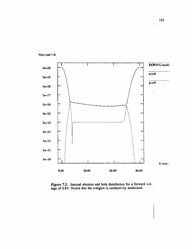
163
N(x) (cmA-3)
le+20
le+19
le+18
le+17
le+16
le+15
le+14
le+13
le+12
l e + l l
le+10
....... . .. .. .._.. . . .. .. . . . .. .. . DOkING.mod1
X (urn)
0.00 10.00 20.00 30.00
Figure 7.2: Internal electron and hole distribution for a forward vol- tage of 0.8V. Notice that the n-region is conductivity modulated.
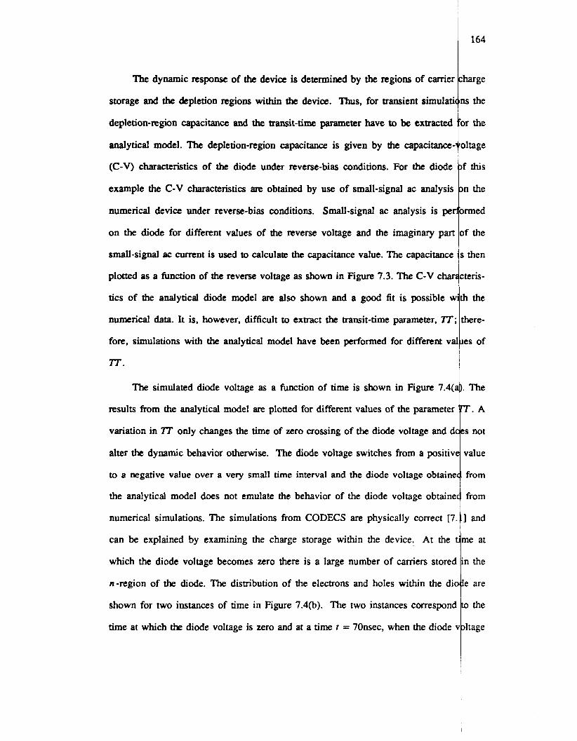
The dynamic response of the device is determined by the regions of carriel
storage and the depletion regions within the device. Thus, for transient simulati
depletion-region capacitance and the transit-time parameter have to be extracted
analytical model. The depletion-region capacitance is given by the capacitance
(C-V) characteristics of the diode under reverse-bias conditions. For the diode
example the C-V characteristics are obtained by use of small-signal ac analysis
numerical device under reverse-bias conditions. Small-signal ac analysis is pel
on the diode for different values of the reverse voltage and the imaginary pari
small-signal ac current is used to calculate the capacitance value. The capacitance
plotted as a function of the reverse voltage as shown in Figure 7.3. The C-V cha~
tics of the analytical diode model are also shown and a good fit is possible v
numerical data. It is, however, difficult to extract the transit-time parameter, 7T
fore, simulations with the analytical model have been performed for different VI
7T.
The simulated diode voltage as a function of time is shown in Figure 7.4(
results from the analytical model are plotted for different values of the parameter
variation in 7T only changes the time of zero crossing of the diode voltage and d
alter the dynamic behavior otherwise. The diode voltage switches from a positi\
to a negative value over a very small time interval and the diode voltage obtain4
the analytical model does not emulate the behavior of the diode voltage obtaint
numerical simulations. The simulations from CODECS are physically correct [S
can be explained by examining the charge storage within the device. At the
which the diode voltage becomes zero there is a large number of camers storec
n-region of the diode. The distribution of the electrons and holes within the di
shown for two instances of time in Figure 7.4(b). The two instances corresponc
time at which the diode voltage is zero and at a time t = 70nsec, when the diode
164
harge
1s the
)r the
,Itage
f this
In the
rmed
I f the
i then
:teris-
h the
here-
ies of
. The
T. A
:s not
value
from
from
1 and
me at
in the
le are
to the
Atage
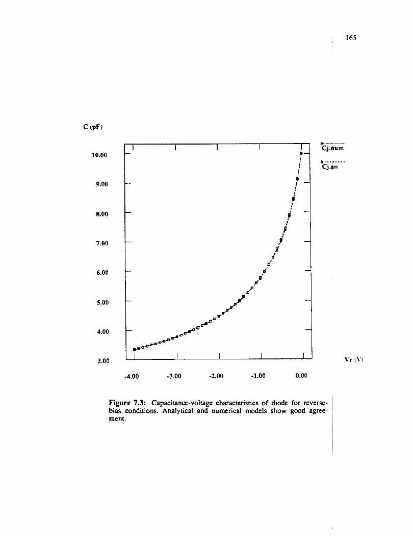
165
c @F)
10.00
9.00
8.00
7.00
6.00
5.00
4.00
3.00 IT I t
-4.00 -3.00 -2.00 -1.00 0.00
* .. .. . ... .. . . . . . Cj.mum
Cj.qn - . - * - - . -
Figure 7.3: Capacitance-voltage characteristics of diode for reverse- bias conditions. Analytical and numerical models show good agree- ment.
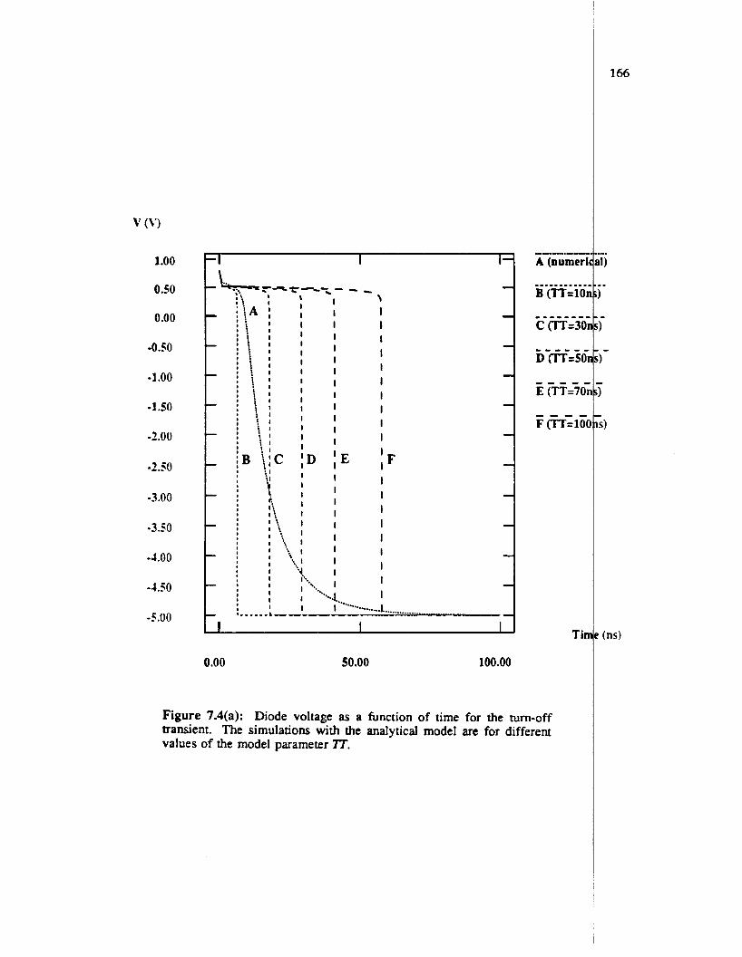
1' (\')
1 .oo
0.50
0.00
-0.50
-1.00
-1.50
-2.00
-2.50
-3.00
-3.10
-4.00
-4.50
-5.00 r I :i I I I
I ... I I 1 :. I 1 1 I I I I
I I 1
8 I. -. * L I -------- I 1 I I
t.. I .'*...* ' I q..
.L ..........___.. I .... ........" I
I1 I 11
0.00 50.00 100.00
Figure 7.4(a): Diode voltage as a function of time for the turn-off transient. The simulations with the analytical model are for different values of the model parameter 7T.
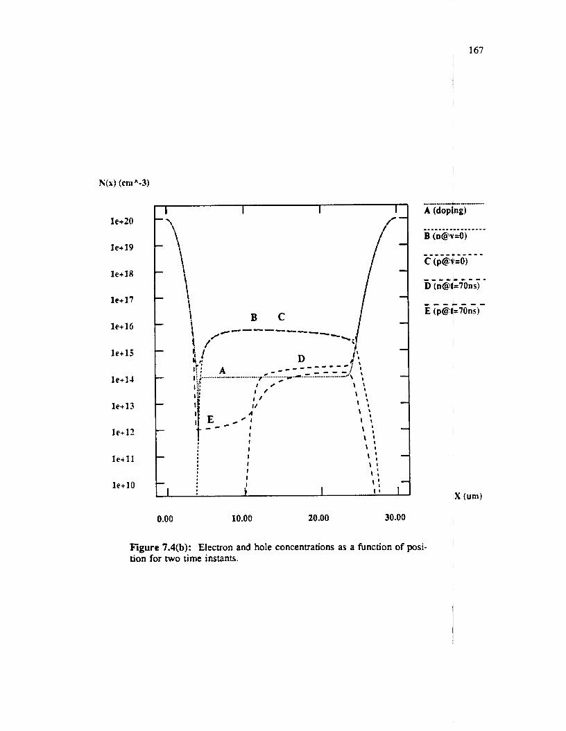
167
le+20
1e+19
le+18
le+17
l e + l 6
l e+ lS
l e + l l
le+13
l e + l ?
l e+ l1
le+10
I- I I
I I I , I
- I I ' ;
I \ I I
0.00 10.00 20.00 30.00
,X (urn)
Figure 7.4(b): Electron and hole concentrations as a function of posi- tion for two time instants.
is near its steady-state value of -5V. It is clear from Figure 7.4(b) that a large
stored charge has to be removed fiom the n-region in addition to the
depletion-region capacitance. This additional charge is responsible for
the diode voltage in Figure 7.4a). The analytical model does not
~ t u r e of the transient voltage across the diode.
73. One-Dimensional Bipolar Transistor Examples
For the simulation examples of this section numerical onedimensional
used for the bipolar transistors. The bipolar transistor is assumed to have a u
ing profile as shown in Figure 7.5(a). Uniform doping is assumed only for
since depletion-region capacitances can be easily calculated. In particular
for abrupt-junction capacitance [7.2] can be used, and the forward transit
be calculated. Although the doping profiles are not realistic they suffice
deficiencies of the analytical bipolar transistor model of SPICE.
The dc current-voltage characteristics obtained from numerical
shown in Figure 7.5(b). Also shown are the characteristics of an anal
Poon model [7.3] that best fits the results obtained from physical simul
agreement exists between the dc characteristics of the analytical and num
To verify that the values of junction capacitances and the transit
for the analytical model are indeed accurate, transient simulations have
on the Oscillator and VCO examples introduced in Chapter 4. The trans
the two circuits simulated by use of analytical and numerical models
ures 7.6 and 7.7. It is seen that the analytical model predicts the freq
tion and the voltage magnitudes in agreement with the numerical mod
ples the transistors are never driven into quasi-saturation or saturatio
analytical model can be used without loss of accuracy. However, wh
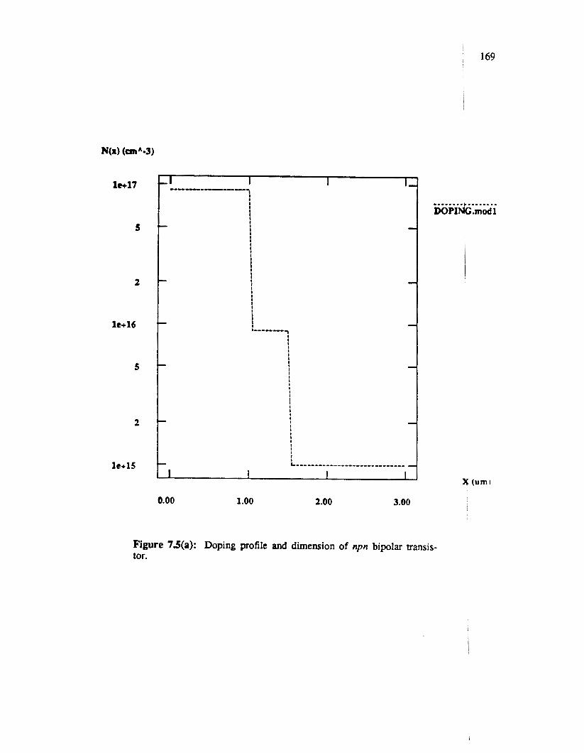
169 I
1-11
5
2
lt+16
5
2
l e+lS
0.00 1.00 2.00 3.00
X (urn)
Figure 75(a): Doping profile and dimension of npn bipolar transis- tor.
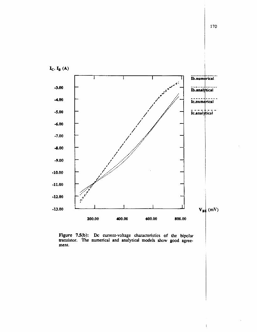
-3.00
-4.00
-5.00
-6.00
-7.00
-8.00
-9.00
-10.00
-11.00
-12.00
-13.00
200.00 400.00 600.00 800.00
Figure 75(b): Dc current-voltage characteristics of the bipolar transistor. The numerical and analytical models show good agree- ment.

, 171
~
vo (VI
7.00
6.50
6.00
5.50
5.00
4.50
4.00
3.50
3.00
Figure 7.6: Simulated transient response for the oscillator circuit. Numerical and analytical models predict an agreement in the voltage magnitude and frequency of oscillation.
I
Time (us)
i !
i
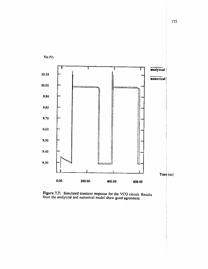
vo (VI
10.10
10.00
9.90
9.80
9.70
9.60
9.50
9.40
9.30
I I I I
0.00 200.00 400.00 600.00
---- rnaly tical
numerical
TiU
Figure 7.7: Simulated transient response for the VCO circuit. Results from the analytical and numerical model show good agreement.
172
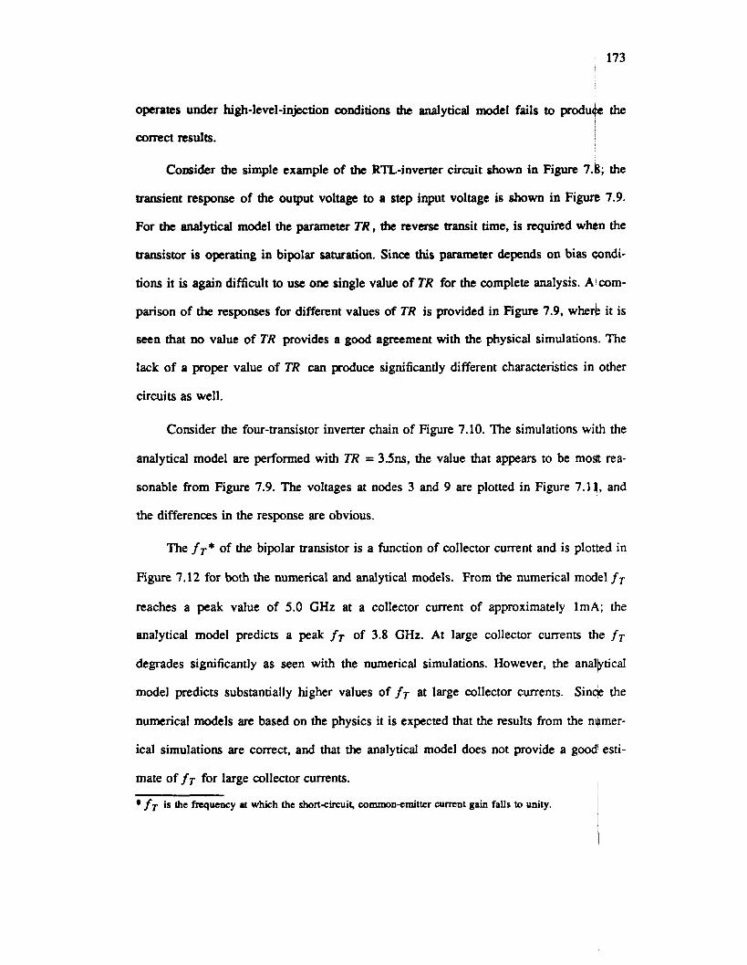
173
operates under high-level-injection conditions the d y t i c d model fails to produde the
comet results. ~
Consider the simple example of the RTL-inverter circuit shown in Figure 7.8; the
transient response of the output voltage to a step input voltage is shown in FigW 7.9.
For the analytical model the parameter TR, the reverse transit time, is required when the
transistor is operating in bipolar saturation, Since this parameter depends on bias @ndi-
tions it is again difficult to use one single value of TR for the complete analysis. A com-
parison of the responses for different values of TR is provided in Figure 7.9, wherk it is
seen that no value of TR provides a good agreement with the physical simulations. The
lack of a proper value of TR can produce significantly different characteristics in other
circuits as well.
Consider the four-transistor inverter chain of Figure 7.10. The simulations with the
analytical model are performed with TR = 3.5ns, the value that appears to be moa rea-
sonable from Figure 7.9. The voltages at nodes 3 and 9 are plotted in Figure 7. l l , and
the differences in the response are obvious.
The fT* of the bipolar transistor is a function of collector current and is plotted in
Figure 7.12 for both the numerical and analytical models. From the numerical model f~
reaches a peak value of 5.0 GHz at a collector current of approximately lmk; the
analytical model predicts a peak fT of 3.8 GHz. At large collector currents the fT
degrades significantly as seen with the numerical simulations. However, the analbdcal
model predicts substantially higher values of fT at large collector currents. Since the
numerical models are based on the physics it is expected that the results from the nJlmer-
ical simulations are correct, and that the analytical model does not provide a good esti-
mate of fT for large collector currents. , I
f is the frequency at which the short-circuit, commoncmitter current gain falls to unity.
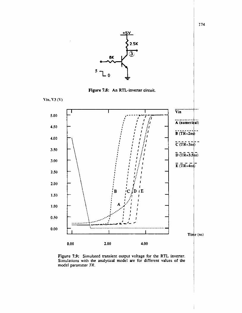
\'in, \13 (V)
5.00
4.50
4.00
3.50
3.00
2.50
2.00
1 S O
1 .oo
0.50
0.00
+5v
- Figure 7.8: An RTL-inverter circuit.
I I
........................................................................... ......-... " .... I I I
0.00 2.00 4.00
Figure 7.9: Simulated transient output voltage for the RTL inverter. Simulations with the analytical model are for different values of the model parameter TR.
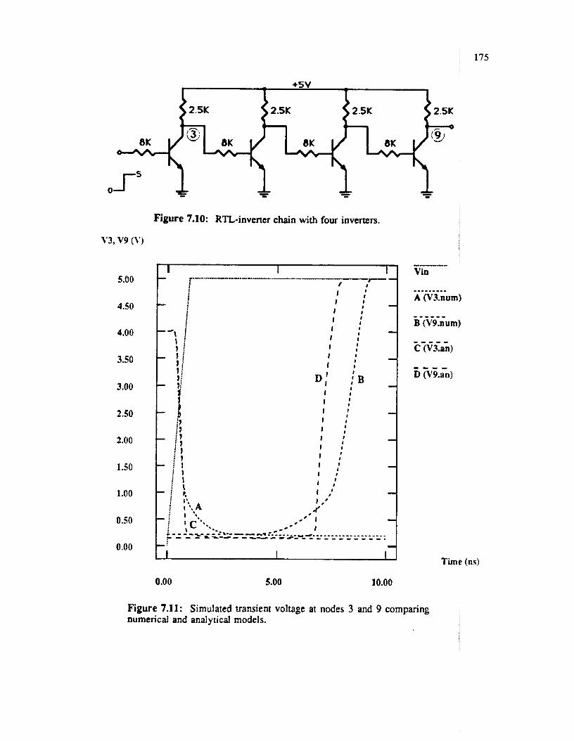
175
0
j'3, v9 (V)
5.00
4.50
4.00
3.50
3.00
2.50
2.00
1 .SO
1.00
0.50
0.00
-
Vin
0.00 5.00 10.00
Figure 7.11: Simulated transient voltage at nodes 3 and 9 comparing numerical and analytical models.
Timt (ns)
I
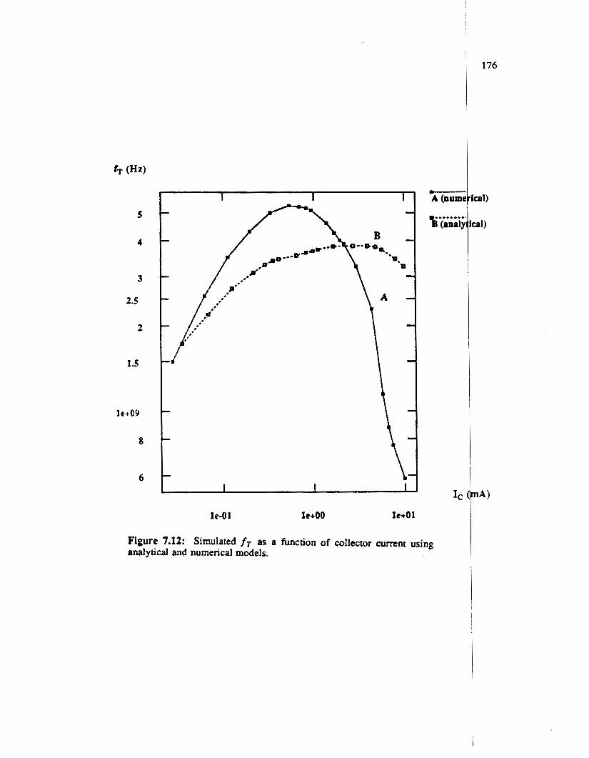
5
4
3
2.5
2
1 .S
le+09
8
6
le-01 le+OO h+01
Figure 7.12: Simulated f~ as a function of collector m n t using analytical and numerical models.
177
I
Another example in which the analytical model will not give accurate resuld is the
operation of the transistor under quasi-saturation conditions. The GP-model daes not
accurately model the base pushout; and, hence, the charge stored in the collector tegion.
Therefore, it does not provide physically accurate results whenever base pushout Wcurs.
High-level-injection conditions are critical to the performance of bipolar transistdrs that
are used to drive large capacitive loads such as the output transistors in BiCMOS or
ECL driver circuits. Shown in Figure 7.13(a) is a BiCMOS driver circuit durihg the
pull-up transient; the bipolar transistor doping profile is again assumed to be unifbrm as
shown in Figure 7.13(b). The bipolar transistor operates under high-level injection in
the collector for large capacitive loads. Base pushout occurs and as a consequence the
current gain decreases and the base transit time increases. The following example once
again illustrates that analytical models that provide a good match in the dc c m n t -
voltage characteristics with numerical models may give considerably different results
under transient simulations. In addition, this example illustrates how numerical hlodels
can be used to evaluate the impact of technological changes on circuit performance, a
task that is very difficult if not impossible to do with analytical models.
The dc current-voltage characteristics for the bipolar transistor, obtained from
numerical and analytical models are shown in Figure 7.14(a). In Figure 7.14(b) ithe dc
current-voltage characteristics of two different transistors are compared; the first tfansis-
tor has the doping profile of Figure 7.13(b) and the doping profile of the second qansis-
tor is given in Figure 7.15. As seen from Figure 7.14(b), the addition of the burie layer
to the original transistor does not alter the dc characteristics and hence the same haly t i -
cal model can be used. The transient response for the two different profiles would'be the
same when computed using the analytical model, whereas the numerical simulations
indicate significantly different operation.
e
.
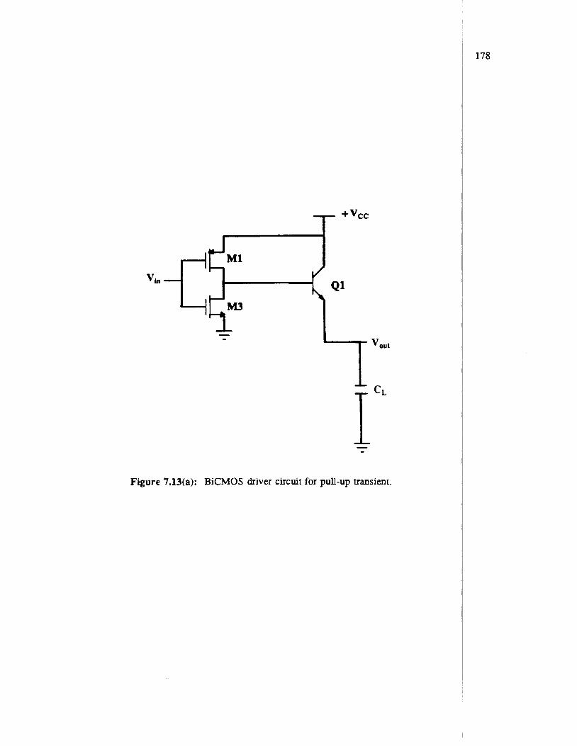
VI"
Figure 7.13(a): BiCMOS driver circuit for pull-up transient.
M1 I U Q1
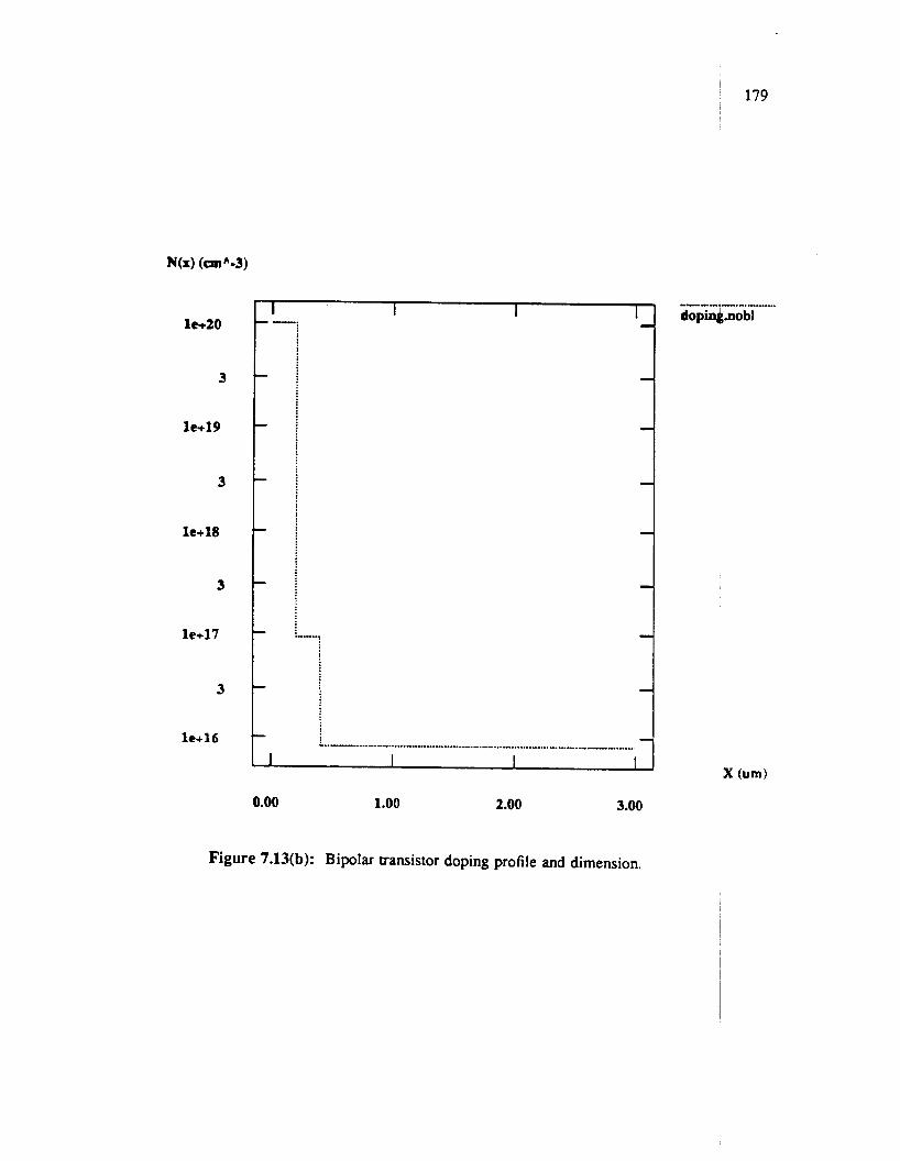
1-20
3
1-19
3
lc+18
3
le+17
3
le+ 16
--'.-..ll..".- ....... dopingsob1
0.00 1.00 2.00 3.00
Figure 7.13(b): Bipolar transistor doping profile and dimension.
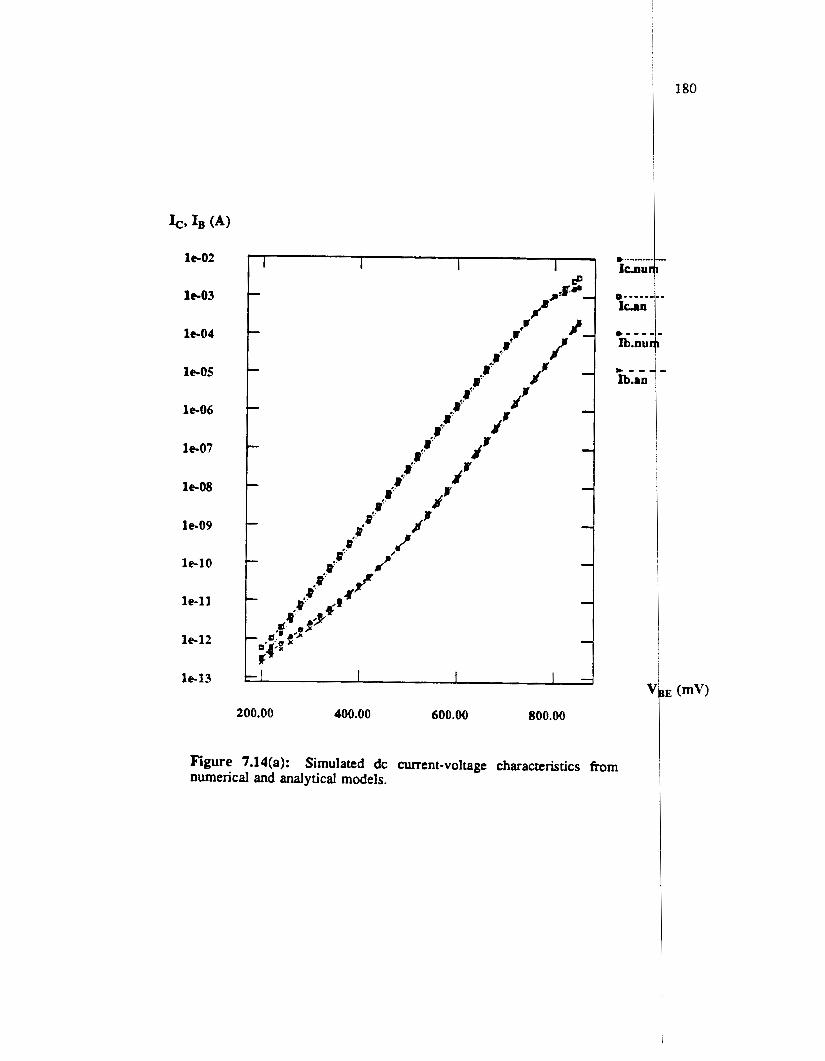
le02
le-03
le-04
le05
le06
le07
le-08
le-09
le10
le-11
le12
le13 I-I 1 I I
400.00 600.00 800.00 200.00
Figure 7.14(a): numerical and analytical models.
Simulated dc current-voltage characteristics from
180
E (mV)
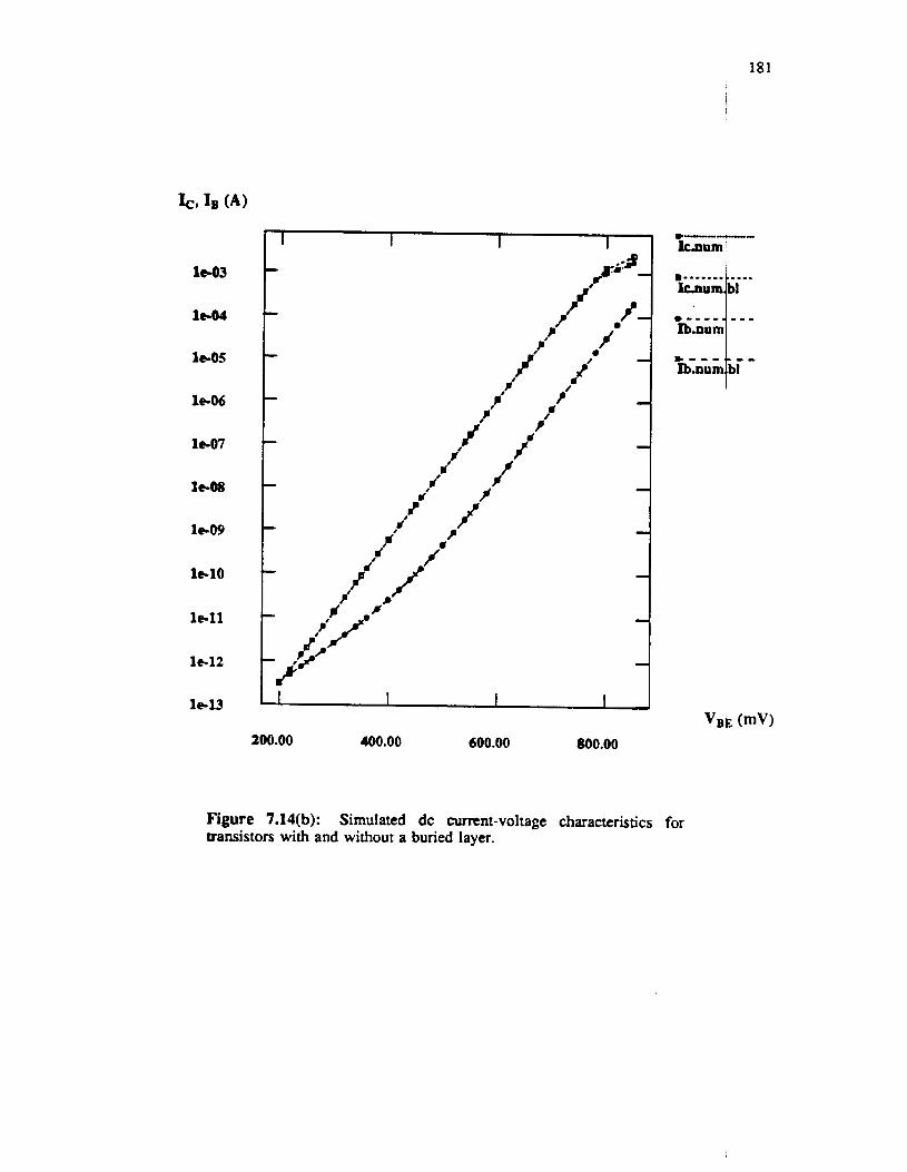
181
l c 9 3
le04
le05
le-06
le07
le08
le09
le10
le-11
le12
le-U
Figure 7.14(b): Simulated dc current-voltage characteristics for transistors with and without a buried layer.
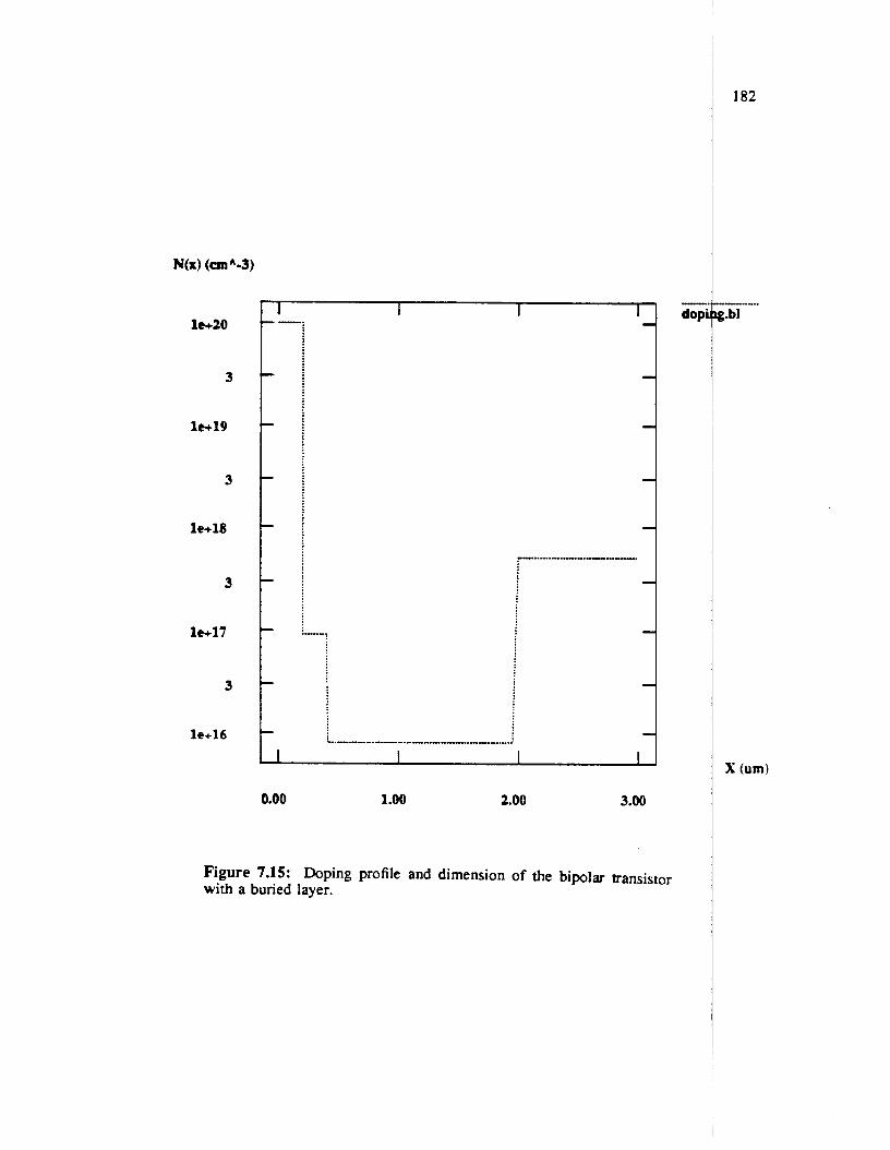
N(x) (mA-3)
1-20
3
1-19
3
le+18
3
1-17
3
le+16 , 0.00 1 .oo 2.00 3.00
Figure 7.15: Doping profile and dimension of the bipolar mansistor with a buried layer.
182
".__....... g.bl
X (urn)

183
In Figures 7.1 q a ) and 7.16@) arc shown the simulated collector current wave(forms
8s a function of time for the pull-up transient The simulations have been p e r f o d d for
two different values of load Capacitance, O.lpF and lOpF, respectively. The $PICE
Level-2 MOS model is used for the MOSFET, and a numerical one-dimnsional Lode1
or the analytical Gummel-Poon model is used for the bipolar transistor. For 'small
values of load capacitance the bipolar transistor operates under low-level-injection bndi-
tions and the simulated collector currents with the three different models an in agree-
ment as Seen in Figure 7.16(a). However, for large values of load capacitance base-
pushout effects become important. The collector currents for the three different aodels
are substantially different in Figure 7.16(b). The numerical models show a distinct roll-
off of collector current at the onset of high-level injection in the collector. The trar)sistor
with the buried layer goes into high-level injection at a larger collector current as seen in
Figure 7.16(b). The simulated results from the analytical model do not depict the same
behavior in collector current, and it is clear that the analytical model cannot be used for
simulation of base-pushout effects. The internal carrier distributions for the two bipolar
transistor profiles are shown in Figure 7.17. The transistor with a buried layer hab less
base pushout compared with the transistor without the buried layer. Therefore, a larger
ament is available to charge up the load capacitance leading to a smaller delay. The
analytical model cannot be used to evaluate the effect of the buried layer, since the dc
characteristics do not change and the same analytical model is applicable to both 'types
of transistor structures.
7.4. Two-Dimensional MOS Examples
CODECS simulation of MOS circuits is presented in this section. Considm the
MOS transistor geomeay shown in Figure 7.18(a) and the two-dimensional d@ping
profile shown in Figure 7.18(b). Again for simplicity uniform doping profile
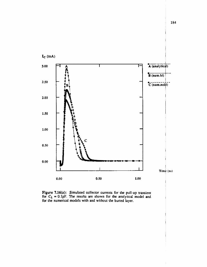
3.00
2.50
2.00
1 S O
1 .oo
0.50
0.00
*.-.--. A (analytic
Tim
0.00 0.50 1.00
Figure 7.16(a): Simulated collector currents for the pull-up transient for C, = O.lpF. The results are shown for the analytical model and for the numerical models with and without the buried layer.
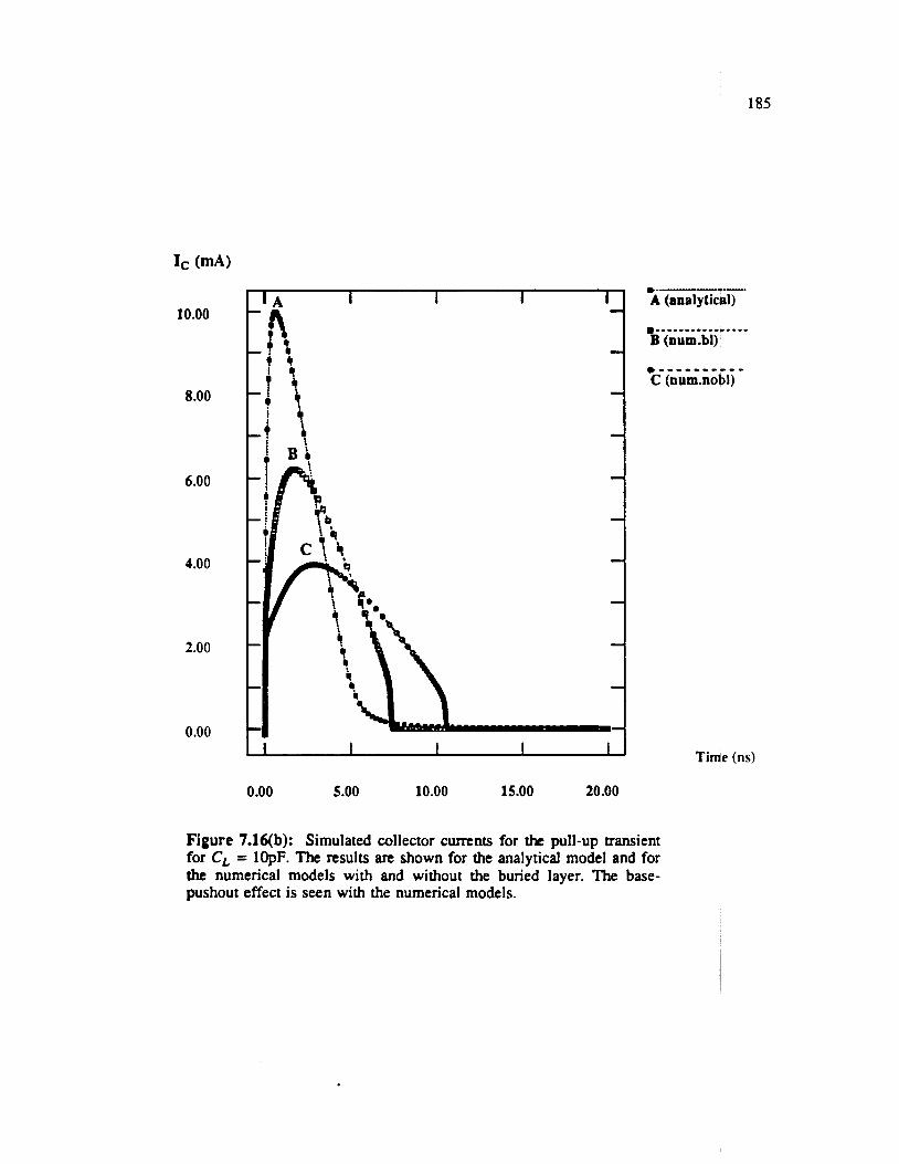
185
IC (m.4
10.00
8.00
6.00
4.00
2.00
0.00
0.00 5.00 10.00 15.00 20.00
Time (ns)
Figure 7.1qb): Simulated collector cumnts for the pull-up transient for C, = IOpF. The results are shown for the analytical model and for the numerical models with and without the buried layer. The base- pushout effect is seen with the numerical models.
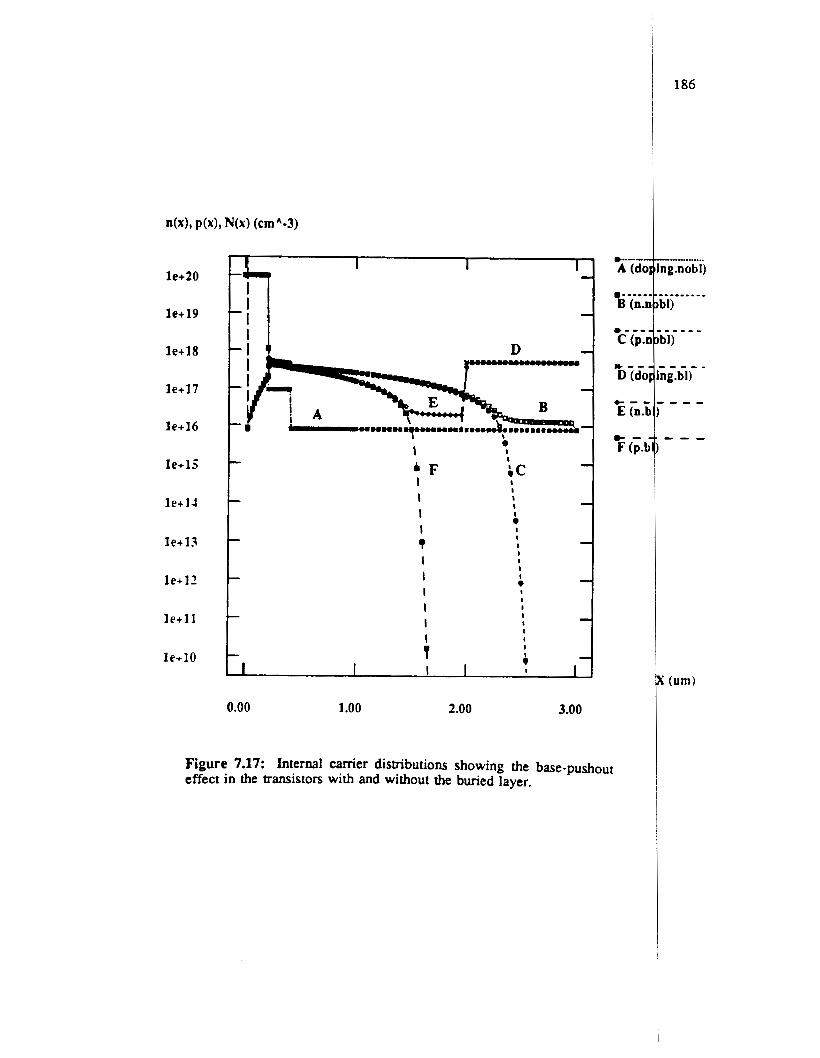
le+20
le+19
le+18
le+17
le+16
l e + l j
l e + l l
le+l . l
le+]?
l e + l l
le+10
0.00 1.00 2.00 3.00
Figure 7.17: Internal camer distributions showing the base-pushout effect in the transistors with and without the buried layer.
186
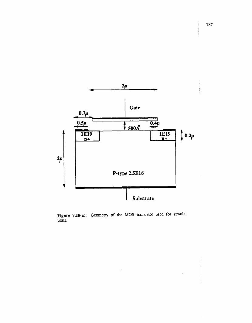
i 187
Gate
P-type 25E16
1 Substrate
Figure 7.18(a): Geomeby of the MOS transistor used for simula- tions.
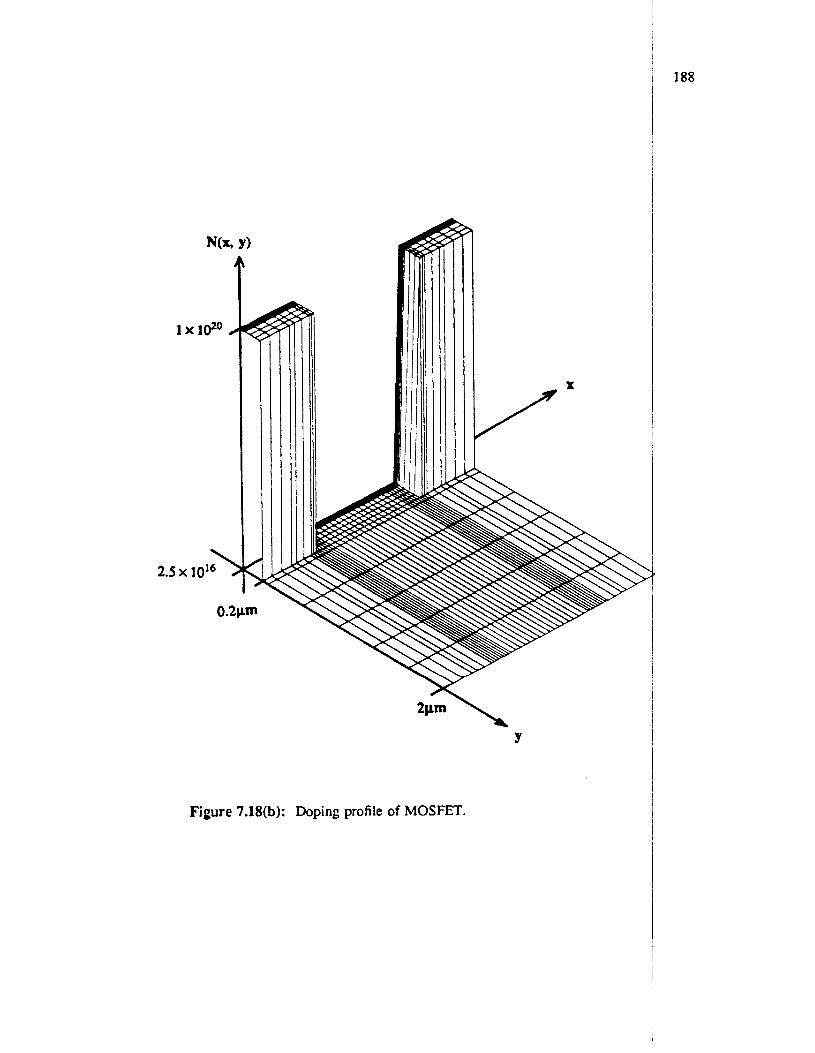
1 X l d O . 1 C
h
Figure 7.18(b): Doping profile of MOSFET.
188
189
assumed as shown. The dc characteristics of the MOS device are shown in Fi& 7.19
where rhe ID-vGs characteristics dtfi the substrate bias as a parameter arc given Fig-
ure 7.19(a) and the ID-vDs characteristics for different gate voltages are given in Figure
7.19(b). Also shown in these figures are the characteristics of the SPICE Level-2~MOS
model that best fits the numerical results. Reasonable agreement is seen betweefn the
characteristics generated from the two models. 1
Charge nonconservation has been of serious concern in MOSFET circuits. /Some
analytical MOS models do not wnserve charge and are not suited to simulatipn of
switched-capacitor circuits, where charge transfers are important. Any MOSFET model
must possess the propmy of charge conservation. In analytical models charge con+erva-
tion can be achieved by use of charge as the state variable [7.4, 7.51. Physical Models
should conserve charge since charge conservation is implied in the basic equation$, and
this is indeed the case. Two examples are used to illustrate charge conservation in the
numerical model. They are the bootstrap circuit of Figure 7.20(a) [7.6] and the dharge
pump circuit of Figure 7.20(b) [7.4]. The first circuit is a simple circuit to study dharge
conservation, whereas the second circuit provides a better test for charge conserCration
since the MOS transistor goes through all its regions of operation. The capacitor vdtages
as a function of time are shown in Figures 7.21(a) and 7.21(b). The capacitor voltage
from the numerical model is maintained at its constant value from cycle to cycle, thereby
depicting that charge is conserved. The SPICE Level-2 MOS model, with the p y e r
capacitance model [7.7], is known to have charge conservation problems [7.4]. 's is
seen to be the case in Figures 7.21(a) and 7.21(b), where the results from the $ vel-2
model are also included; a shift in the capacitor voltages can be seen due to noncbnser-
vation of charge.
~
Next consider the turn-on and turn-off transients of a MOS transistor; the sipula-
tions are performed by use of the simple circuit of Figure 7.22. The gate volt
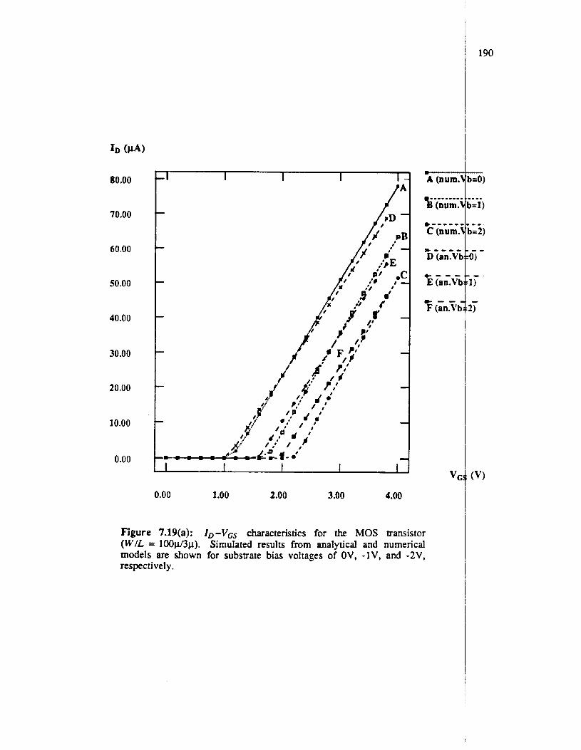
ID (FA)
80.00
70.00
60.00
50.00
40.00
30.00
20.00
10.00
0.00 I I I
0.00 1.00 2.00 3.00 4.00
Figure 7.19(a): ID -Vcs characteristics for the MOS transistor ( W / L = 10Opl3p). Simulated results from analytical and numerical models are shown for substrate bias voltages of OV, -1V, and -2V, respectively.
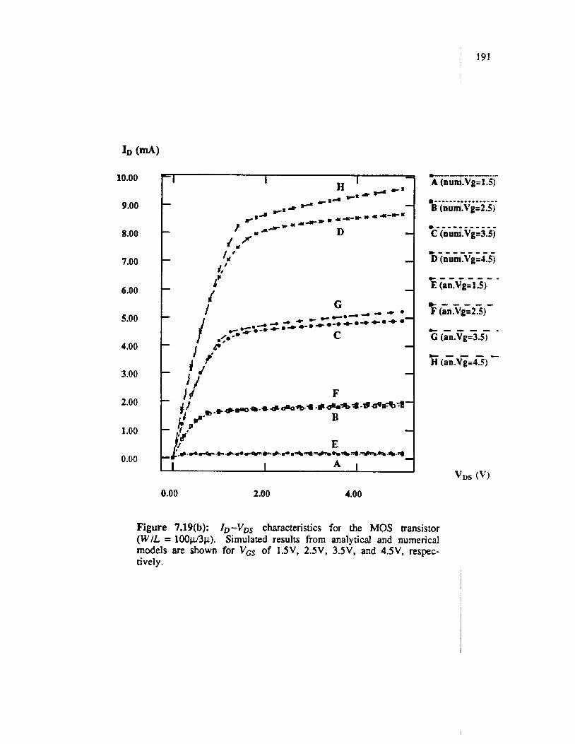
191
10.00
9.00
8.00
7.00
6.00
5.00
4.00
3.00
2.00
1 .oo
0.00
0.00 2.00 4.00
Figure 7.19(b): ID -VDS characteristics for the MOS transistor ( W i t = lOOcl/3~~). Simulated results from analytical and numerical models are shown for VGS of 1.W, 2SV, 3SV, and 4SV, respec- tively.
vDS (v)
i I
i
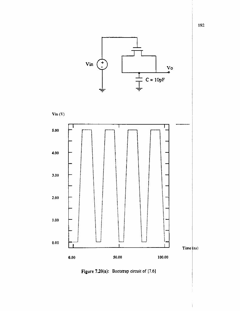
Vin (Y)
r
vo i e
5.00
4.00
3.00
2.00
1 .oo
0.00
Vin
I 1
0.00 50.00 100.00
Figure 7.20(a): Bootstrap circuit of [7.6]
...-......
Time
192
3s)
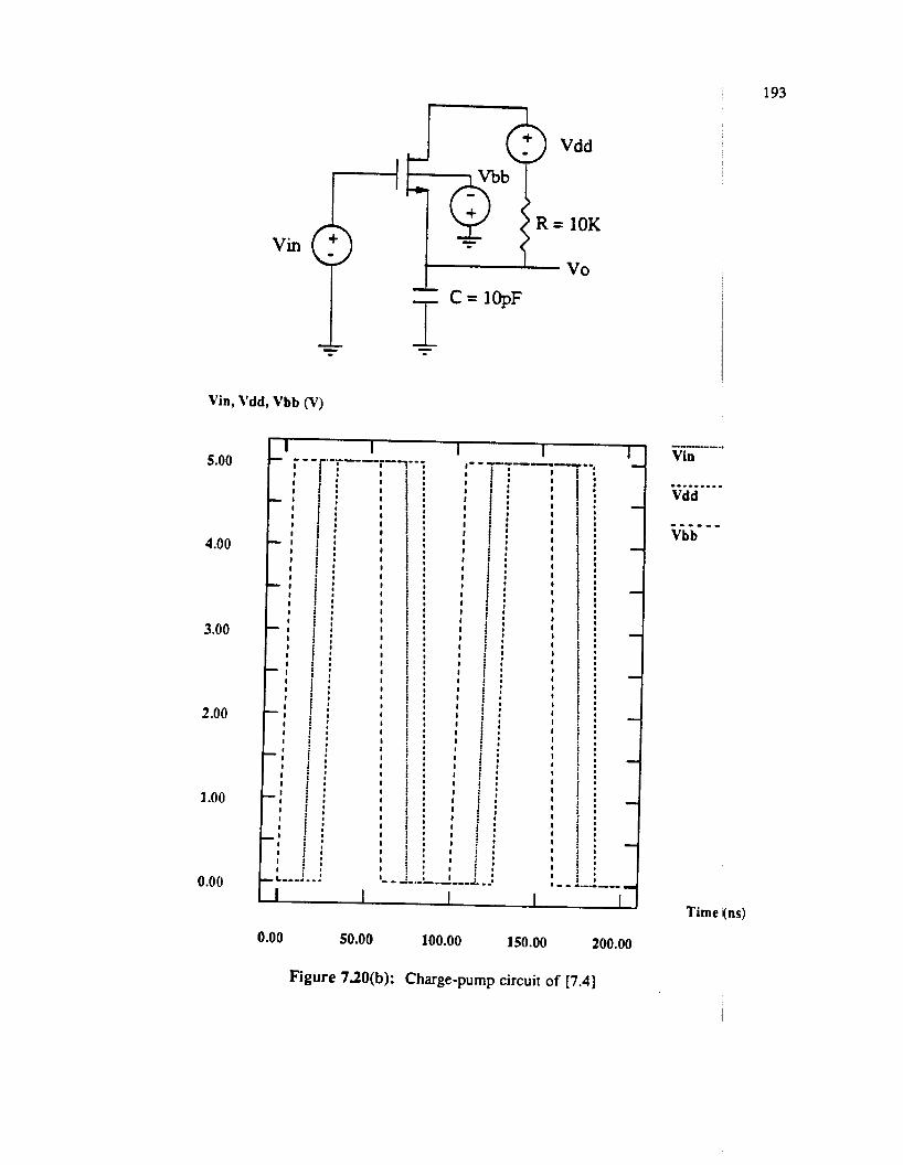
193
J 8 Vdd
Vin
Vin. Vdd, Vbb
500
4.00
3.00
2.00
1 .oo
0.00
-L ,- C = lOpF
J
--....-.. Vin
I I I I I I I I I I I I I I I I I I I I I I I I I I I I I 1 I I I I I I I I I I I I I I I I I
1- - .
I I I I I I I I I I I I I I I I I I I I I I I I I I I I I I I I I I I I I I I
I 1 I I I I I I I I I I I I I I I I I I I I I I I I I 1 I I I I I I I I I I I I I I I I I I I I
Time i(ns)
0.00 50.00 100.00 150.00 200.00
Figure 730(b): Charge-pump circuit of [7.4]
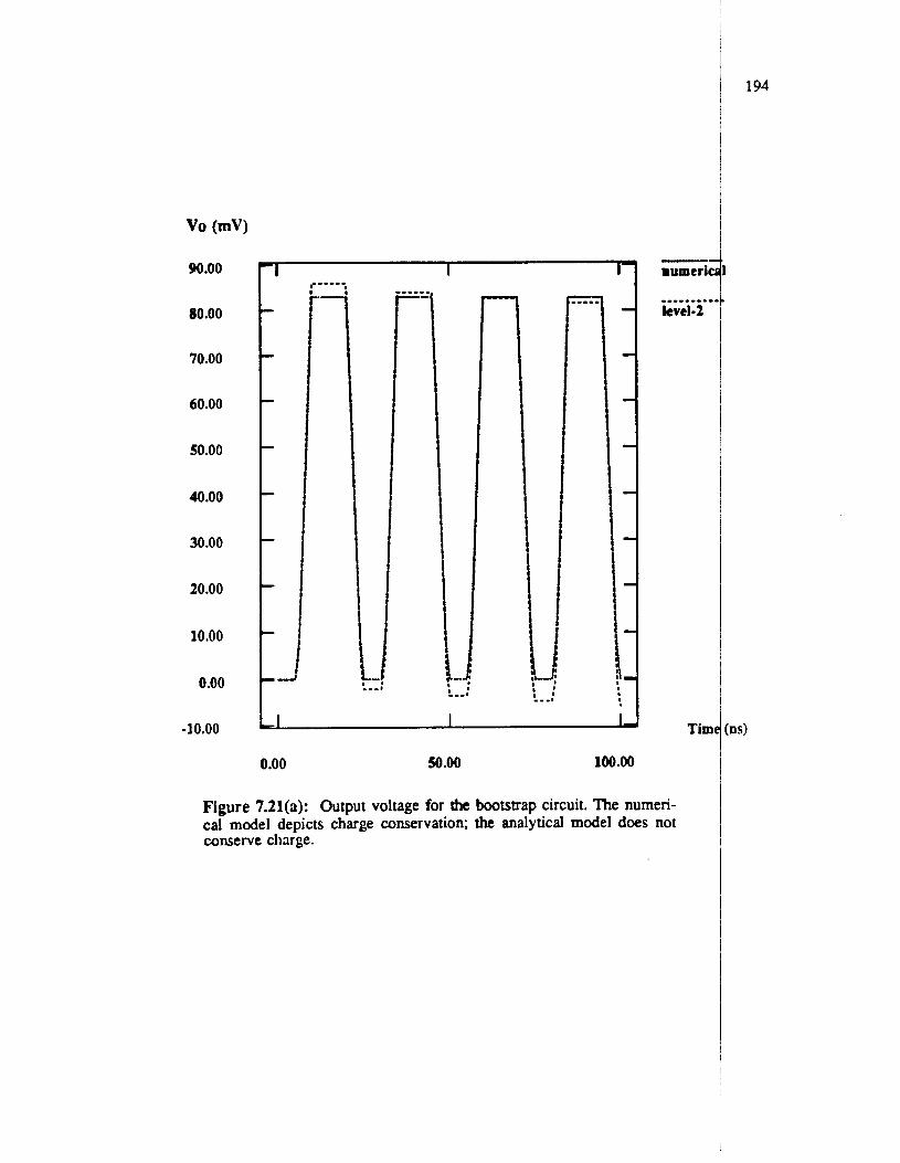
Vo (mV)
90.00
80.00
70.00
60.00
50.00
40.00
30.00
20.00
10.00
0.00
-10.00
.---- I I
mumetic
kvel-2 ..-- .... .
Tim
0.00 50.00 100.00
Figure 7.21(a): Output voltage for the bootstrap circuit. The numeri- cal model depicts charge conservation; the analytical model does not conserve charge.
194
ns)
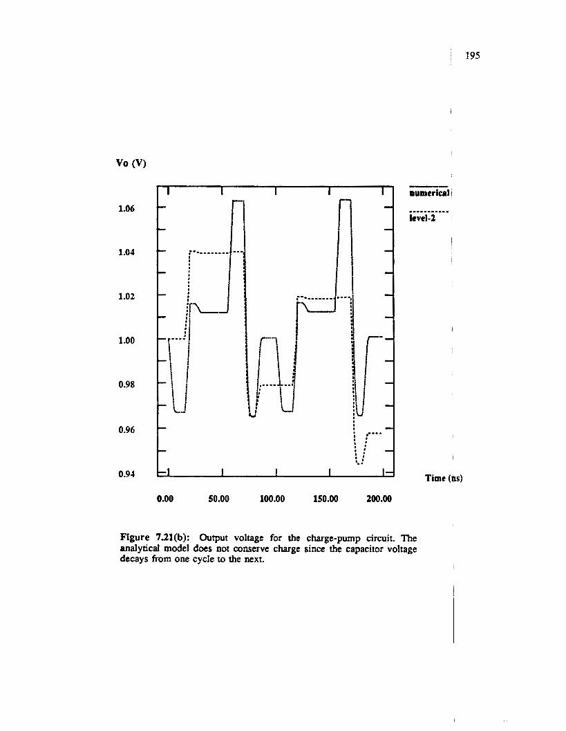
195
vo (VI
1.06
1.04
1.02
1.00
0.98
0.96
0.91
Figure
i a
numerical I
kvel-2 -..-----...
I
I
Time (os)
0.00 50.00 100.00 150.00 200.00
731(b): Output voltage for the charge-pump circuit. The analytical model does not anserve charge since the capacitor voltage decays from one cycle to the next.
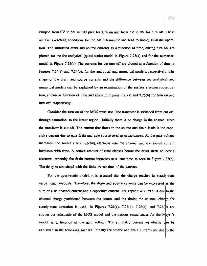
ramped from OV to 5V in 100 psec for twm on and from SV to OV for turn off.
are fast switching conditions for the MOS transistor and lead to non-quasi-static
196
These
opera-
The delay is associated with the finite transit time of the carriers.
For the quasi-static model, it is assumed that the charge reaches its
value instantaneously. Therefore, the drain and source currents can be expressed
sum of a dc channel current and a capacitive current. The capacitive current is due
channel charge partitioned between the source and the drain; the channel char~e
steady-state operation is used. In Figures 7.26(a), 7.26(b), 7.26(c), and 7.26(11)
steady-state
as the
to the
for
are
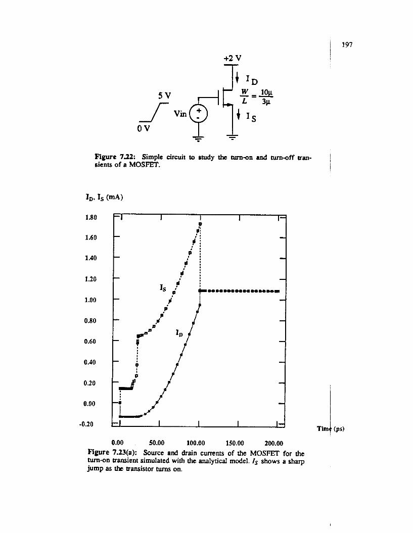
~ 197 I I
+2 v 1
ov
Figure 7.22: Simple circuit to study the tum-on and turn-off tran- sients of a MOSFET.
1.80
1.60
1.40
1.20
1 .oo
0.80
0.60
0.40
0.20
0.00
-0.20
0.00 50.00 100.00 150.00 200.00 Figure 733(a): Source and drain currents of the MOSFET for the turn-on transient simulated with the analytical model. 1s shows a sharp jump as tht transistor turns on.
Tim
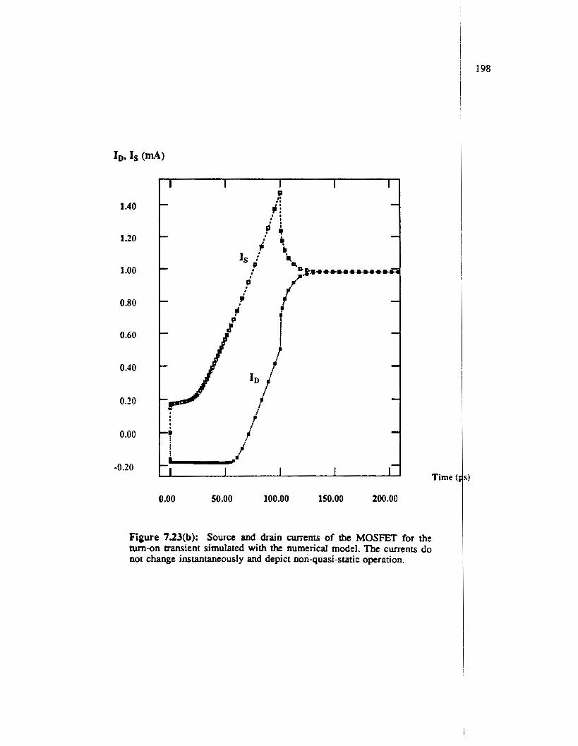
1.40
1.20
1 .oo
0.80
0.60
0.40
0.20
0.00
-0.20
0.00 50.00 100.00 150.00 200.00
Time (
Figure 733(b): Source and drain currents of the MOSFET for the turn-on transient simulated with the numerical model. The currents do not change instantaneously and depict non-quasi-static operation.
198
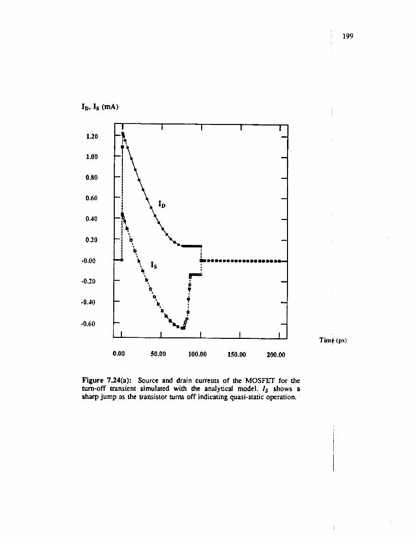
199
1.20
1.00
0.80
0.60
0.40
0.20
-0.00
-0.20
-0.40
-0.60
0.00 50.00 100.00 150.00 200.00
Figure 7.24(a): Source and drain currents of the MOSFET for the turn-off transient simulated with the analytical model. Is shows a sharp jump as the transistor turns off indicating quasi-static operation.
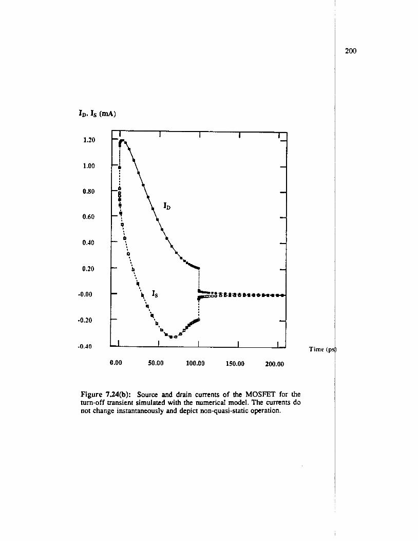
1.20
1 .oo
0.80
0.60
0.40
0.20
-0.00
-0.20
-0.40
0.00 so.00 100.00 150.00 200.00
Figure 7.24(b): Source and drain currents of the MOSFET for the turn-off transient simulated with the numerical model. The currents do not change instantaneously and depict nonquasi-static operation.
Time (p
200
I
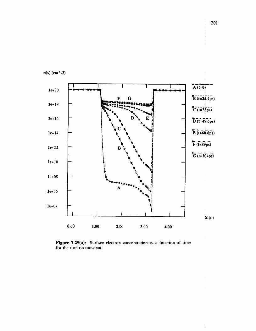
201
le+20
le+18
le+16
l r + l l
le+]?
le+10
le+O8
l e + M
le+Ol
0.00 1.00 2.00 3.00 4.00
Figure 735(a): Surface electron concentration as a function of time for the turn-on transient.
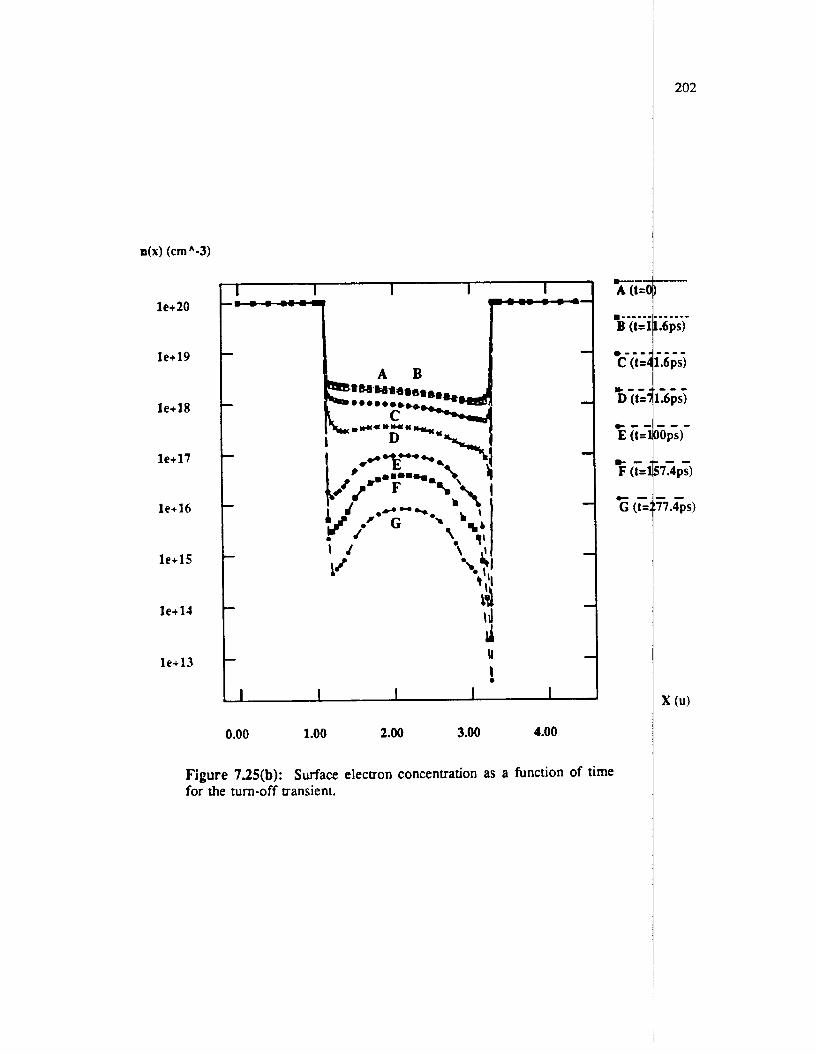
a(x) (cm A-3)
le+tO
le+19
le+18
le+17
le+16
l e+ lS
l e + l J
1e+13
0.00 1.00 2.00 3.00 4.00
Figure 725(b): Surface electron concentration as a function of time for the turn-off transient.
--- A (1:
B (1:
c (1'
D (t:
E (1:
F (t:
G (t
me- - -
e--,
* - -
t -
D - -
c -
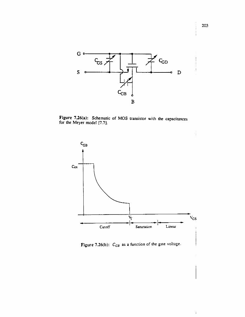
203
B
Figure 726(a): Schematic of MOS transistor with the capacitances for the Meyer model 17.71.
Figure 7.26(b): CGs as a function of the gate voltage.
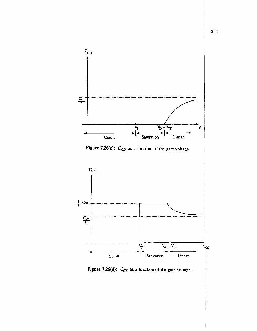
%D
...........................................................................................
I c c cutoff 4 saturation ' Linear
Figure 7.26(c): CGD as a function of the gate voltage.
Es
-$ C O X
Figure 726(d): CGs as a function of the gate voltage.
204
S
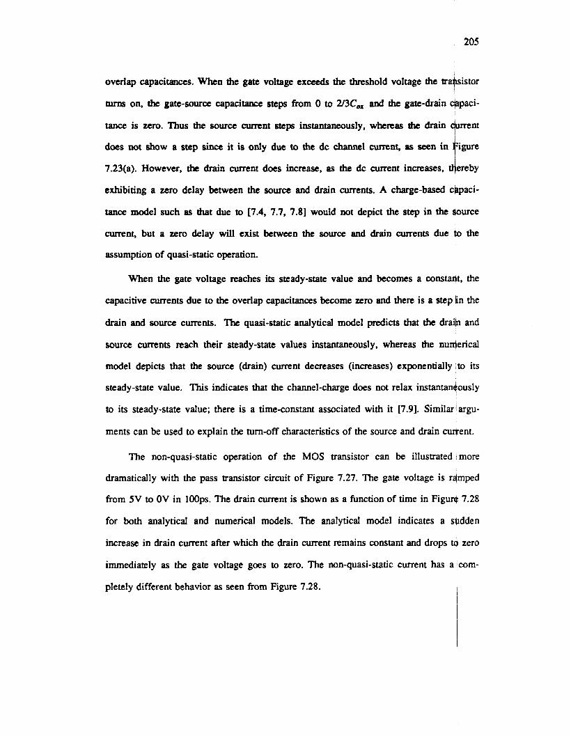
205
overlap capacitances. When the gate voltage exceeds the threshold voltage the tra+istor
turns on, the gate-source capacitance steps from 0 to U3C, and the gate-drain +pa&
tance is zero. Thus the source cumnt steps instantaneously, whereas the drain m n t
does not show a step since it is only due to the dc channel current, as seen in igure
7.23(a). However, the drain current does increase, as the dc current increases, dereby
exhibiting a zero delay between the source and drain currents. A charge-based chpaci-
tance model such as that due to [7.4, 7.7, 7.81 would not depict the step in the rlource
current, but a zero delay will exist between the source and drain currents due the
assumption of quasi-static operation.
T
When the gate voltage reaches its steady-state value and becomes a conswt, the
capacitive currents due to the overlap capacitances become zero and there is a step Cn the
drain and source currents. The quasi-static analytical model predicts that the drailn and
source currents reach their steady-state values instantaneously, whereas the nu4erical
model depicts that the source (drain) current decreases (increases) exponentially to its
steady-state value. This indicates that the channel-charge does not relax instantan&ously
to its steady-state value; there is a timeanstant associated with it [7.9]. Similar'argu-
ments can be used to explain the turn-off characteristics of the source and drain cwent.
The non-quasi-static operation of the MOS transistor can be illustrated more
dramatically with the pass transistor circuit of Figure 7.27. The gate voltage is rdmped
from 5V to OV in loops. The drain current is shown as a function of time in Fig@ 7.28
for both analytical and numerical models. The analytical model indicates a sqdden
increase in drain current after which the drain current remains constant and drops to zero
immediately as the gate voltage goes to zero. The non-quasi-static current has aicom-
pletely different behavior as seen from Figure 7.28.
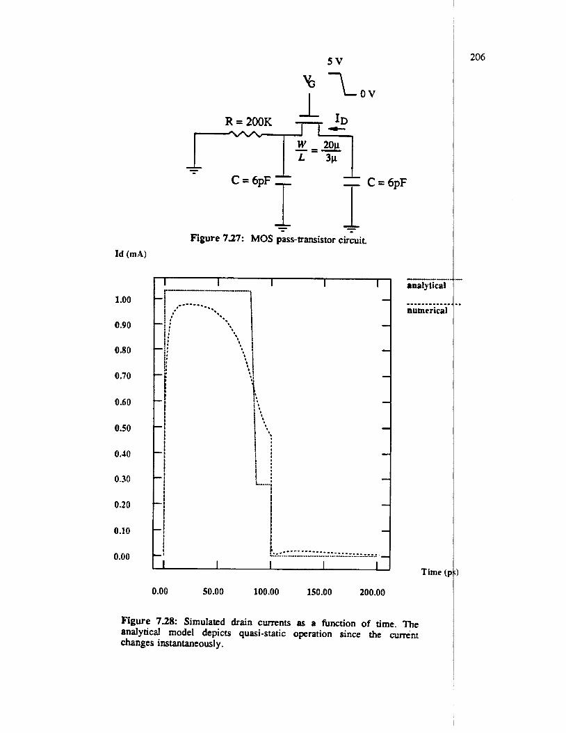
S V
C = 6pF
Figure 7.27: MOS pass-transistor circuit. Id (mA)
1.00
0.90
0.80
0.70
0.60
0.50
0.40
0.30
0.20
0.10
0.00
0.00 50.00 100.00 150.00 200.00
--........... analytical
numerical .---..-----.
Time (J
The Figure 7.28: Simulated drain currents as a function of time. ' analytical model depicts quasi-static operation since the Current changes instantaneously.
206
207
75 . Runtime Comparisons with Analytical Models I
Simulation with analytical models will always be faster in performance co@pared
to that with numerical models. This is to be expected since analytical model only
require function evaluations to compte the conductances and currents of a &vice/ with
a numerical model the device-level matrix has to be decomposed into its LU factobs and
forward and back substitutions are required to compute the currents and conduc+nces.
The latter task requires more CPU time resulting in the higher computational cost soci-
ated with numerical models. However, under several situations an analytical mo 1 may
give inaccurate results due to its simplicity in modeling the actual physical behavi 4 r of a
device. Thus a comparison between numerical and analytical models is not appropriate.
Numerical models will be used only in situations where analytical models are bade-
quate, and computation cost should not be of concern when accuracy is d&sired.
Nonetheless, the comparison is given to provide an estimate of the increase in co+puta-
tional effort when using a numerical model.
1
In Table 7.1 a comparison is presented between numerical and analytical rhodels
for the benchmark examples. The results for the numerical simulation are obtainled by
the use of trapezoidal integration method. The numbers for the various examples iare in
the following sequence: number of iterations, number of timepoints accepted, number of
timepoints rejected, total number of timepoints, and the runtimes in seconds on a'VAX
8800. From Table 7.1 it is clear that the numerical models require a larger number of
timepoints; and, hence, a larger number of iterations. Numerical models require larger
number of timepoints because they are solving for the Poisson's and the electrob and
hole current-continuity equations, which have time constants that are quite different1 from
the circuit. Since the timesteps are decided based on the activity internal to a d vice, e smaller timesteps will be used to resolve accurately the carrier concentrations, req
a larger number of timepoints to complete the transient analysis.
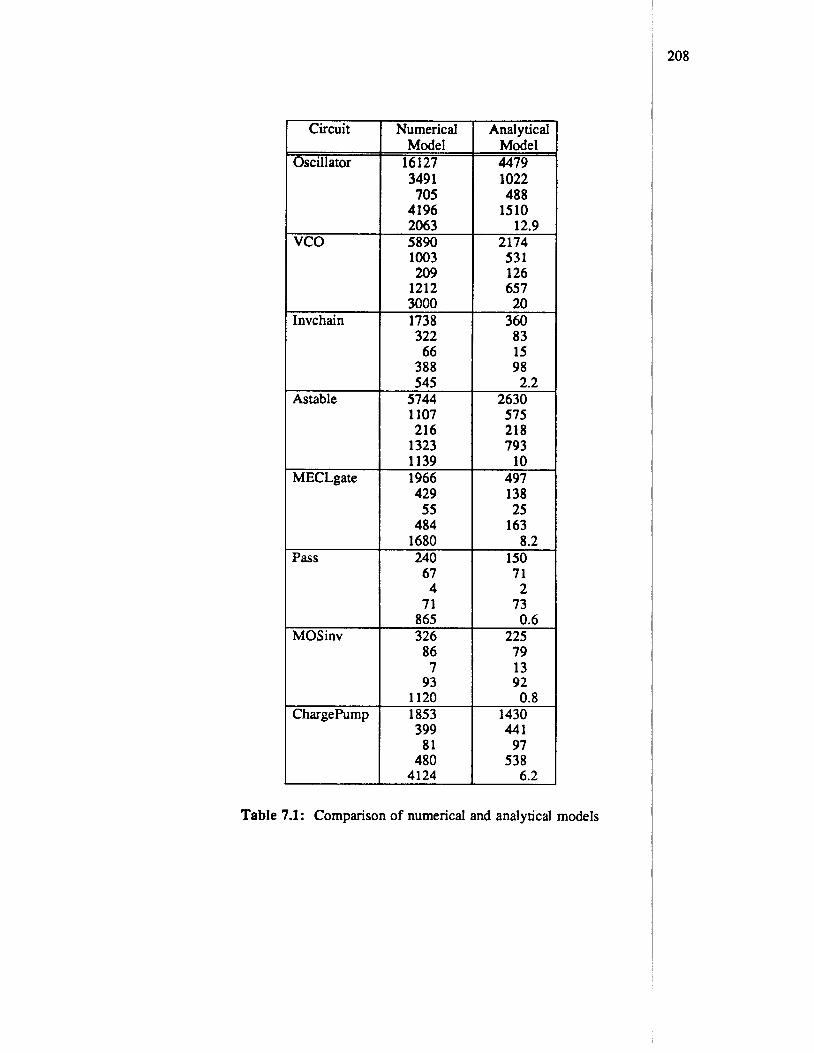
Circuit
Oscillator
vco
Invchain
Astable
MECLgate
1 Numerical I Analytical
Pass
MOSinv
Chargehmp
Model 16127
Mddel 4479
349 1 705
4196
1022 488
1510 2063 I 12.9 5890 2174 1003 209
1212 3000 1738 322 66
388 545
5744 1107 216
1323
53 1 126 657 20
360 83 15 98
2630 575 218 793
2.2
1139 1966
10 497
429 55
484 1680 240 67 4
71
138 25
163
150 71
2 73
8.2
Table 7.1: Comparison of numerical and analytical models
865 326
208
0.6 225
86 7
93 1120 1853 399 81
480 4124
79 13 92
1430 441 97
538
0.8
6.2
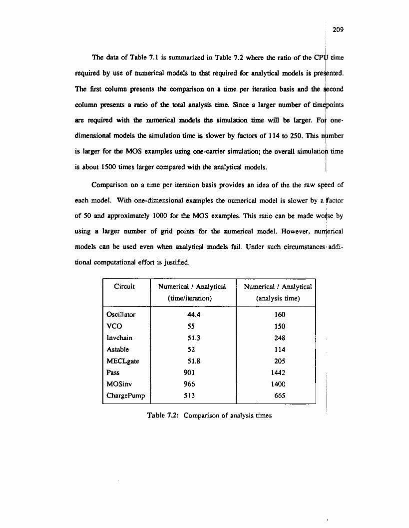
209 ,
The data of Table 7.1 is summarized in Table 7.2 where the ratio of the CP time
required by use of numerical models to that required for analytical models is pre nted.
column presents a ratio of the total analysis time. Since a larger number of tim ints
are required with the numerical models the simulation time will be larger. Fo one-
dimensional models the simulation time is slower by factors of 114 to 250. This n mber
is larger for the MOS examples using o n e d e r simulation; the overall simulatio time
The first column presents the comparison on a time per iteration basis and the
is about 1500 times larger compared with the analytical models. ~
Comparison on a time per iteration basis provides an idea of the the raw spked of
each model. With one-dimensional examples the numerical model is slower by a factor
of 50 and approximately 1000 for the MOS examples. This ratio can be made wotse by
using a larger number of grid points for the numerical model. However, nuwerical
models can be used even when analytical models fail. Under such circumstancesladdi-
Circuit
tional computational effort is justified.
Numerical / Analytical (timehration)
Oscillator
vco Invchain Astable
MECLgate Pass MOSinv Chargepump
44.4
55
51.3
52
51.8
901
966
513
Numerical / Analytical (analysis time)
160
150
248
114
205 1442
1400
665
Table 7.2: Comparison of analysis times
210
A tradeoff between runtimes and simulation accuracy can be achieved by m
only the critical devices numerically and using analytical models for the rest of
cuit. The BiCMOS driver circuit is a typical example of such an approach. Since
ing of bipolar transistors is critical for simulations, numerical models have been
the bipolar transistor, whereas the MOSFET is modeled by an analytical model.
two-dimensional numerical MOSFET model would not have provided
into the operation of the circuit. Mixed-level simulation allows the use
lation models for the critical devices and less accurate but faster
ca1 devices.
21 1
CHAPTER 8
Applications of CODECS
I 8.1. Introduction
A variety of applications of CODECS are presented in this chapter. The a lica-
tions span from use of only the device-simulation capability to use of the mixed-level +
circuit and device-simulation environment. All of these applications demonstrate use-
fulness of CODECS as a simulation program. In addition, CODECS can be uged to
evaluate technology tradeoffs; hence, it provides a predictive capability.
I
I
The first application illustrates the use of CODECS for estimating the de ay of
BiCMOS driver circuits. While driving large capacitive loads, the bipolar tranfistors
operate in high-level injection. As indicated in Chapter 7, commonly available gPICE
bipolar transistor models are inadequate for simulating high-level-injection effects c$itical
i
to the operation of BiCMOS circuits. Therefore, SPICE simulations cannot be u$ed to
accurately estimate the delay. With the use of physical models in CODECS, howeker, it I
is possible to analyze the delay and to evaluate the effect of technology and suppl vol-
tage scaling on the delay of the BiCMOS driver. Y I
The second application concerns power devices. Simulation examples in Chapter 7
show that the SPICE diode model is inadequate to study the turn off of pi-n
a resistive load. For an inductive load, the situation is even more
quently, the problem is extremely difficult to model analytically
circuit simulation provides a way to study the turn-off
of pi-n rectifiers is investigated. CODECS is also used to study the transient
down of pi-n rectifiers with an inductive load. Oscillations are observed when
is near the breakdown voltage. A physical model is used to explain this
based on insight gained fiom CODECS simulations.
The problem of charge injection in MOS switched-capacitor circuits is exam
Section 8.4. The numerical MOS model in CODECS conserves charge and does
an empirical scheme for channel-charge partitioning. Therefore, the charge that flows
of the various terminals of a MOSFET during the turn off is calculated accurately,
CODECS can be used to study switch-induced error voltages. Thus, different
cancellation schemes can be evaluated in terms of their effectiveness in reduci.ng
switch error. Although analytical results are available under very specific conditicns,
general solution exists. CODECS can be used to simulate realistic driving sow%
tions. In addition, it also allows simulation of nonquasi-static MOS operation
influence the charge transfer in switchedcapacitor circuits. A comparison of the
cal and numerical MOS models in Chapter 7 demonstrated the inadequacy of a
MOS models for non-quasi-static operation.
As a last application, CODECS is shown to be a tool that can be used
analytical models. The numerical models can be used as a reference with
which analytical models can be evaluated. An analytical model for the late
field in lightly doped drain MOSFETs and a non-quasi-static MOSFET mod
as examples of such an application.
82. Analysis of BiCMOS Driver Circuits
The BiCMOS driver circuit shown in Figure 8.1 is a common configura
BiCMOS circuits. This gate is used in static memories 18.11 and gate arr
drive large output capacitors. For large capacitive loads the collector cu
break-
opxation
phenomena
ned in
rot use
out
and
error-
the
no
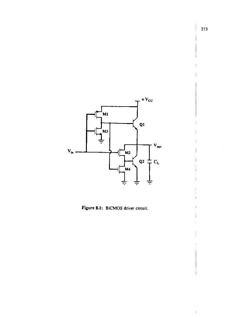
Vi"
Figure 8.1: BiCMOS driver circuit.
' 213
I
I 1
I
I
I
,
I
,
I
I
large and the bipolar transistor operates in high-level injection in the collectoi
quasi-saturation or Kirk effect [8.3, 8.41. SPICE simulations are inadequate since
level-injection effects critical to the performance of the bipolar transistors are not
rately modeled with commonly available SPICE bipolar transistor models. Simul
from CODECS can be used since base pushout under high-level injection is pn
modeled with the numerical bipolar transistor models. In addition, CODECS simul
can be used to study the effect that IC fabrication technology and supply voltage s
have on the delay of the gate.
The delay of the BiCMOS driver depends on the region of operation of the t
transistors. Three different regions of operation exist, namely, operation undei
level-injection conditions, operation in high-level injection, and collector-resistance
inated operation. The relative values of the device parameters and the load capac
determine the operating region of die bipolar transistors. Although various delay r
have been considered for the BiCMOS buffer circuit, they are restricted to one reg
operation. In [8.5] only high-level-injection effects in the base region are corn
which are not as important as the high-level-injection effects in the collector region
analysis of [8.6], on the other hand, considers only the collector-resistance dom
case and assumes that high-level-injection effects do not occur. In practice, while c
large load capacitors both high-level injection in the collector and the collector resi
must be taken into account.
8.2.1. Delay Analysis
A delay model is necessary to identify the important bipolar device paramete
their effect on the performance of the gate. CODECS simulations provide a mea
verifying analytical delay formulas. In this section the delay for operation under
level injection is examined. A detailed analysis for the other regions is available in
214
i.e.,
high-
KCU-
#tiOnS
PerlY
. t iOnS
ding
Polar
low-
dom-
tance
odels
on of
3ered
The
nated
iving
tance
i and
s for
high-
8.71.
215
The delay of the BiCMOS driver is a function of both the MOSFET and 4 bipo-
lar transistor parameters. For the bipolar transistor the parameters that influence thd delay
are: the current gain, 8 (a function of the collector current), the base transit tifne, zf
(also a function of the collector ament), the collector Current at onset of hig -level
injection in the collector, I, , and the pas i t ic capacitances and resistances. h r the
MOSFET the parameters are: the transconductance parameter k', the WIL, the weshold
voltage, V T , and the parasitic capacitances. The delay of the gate is estimated as t func-
tion of these parameters.
Consider the pull-up transient of the gate, the circuit diagram for the pull-upicircuit
is shown in Figure 8.2. The pull-down transient is similar and will not be considered.
The input voltage is stepped from VDD to OV and the MOS transistor turns on. The
MOSFET can be replaced by a current source of value equal to the average MQSFET
current and the circuit to be analyzed is shown in Figure 8.3. If the transit timeiof the
transistor is small, this circuit can be analyzed by modeling the degradation in B ldue to
the base-pushout effect. However, as shown later, the transit-time effects canhot be
ignored when base pushout o c c u s and the analysis based on p degradation dotes not
suffice.
Assume that the load capacitor is initially uncharged and that the transit-time
effects are negligible, the delay can then be expressed as
where I is the average Current of the MOS transistor, C1 is the total capacitance at the
base of the bipolar transistor, C, is the total output load capacitance, Vs is the butput
voltage swing, and I , is the collector current. The first term accounts for the time
required to charge up the base of the bipolar transistor to VBE(~,,) and is the timd taken
to charge c1 to a voltage V,,(,,,, with a m n t ID. The second term models th
7- +vcc
I -
Figure 8.2: Circuit diagram of the pull-up circuit.
216
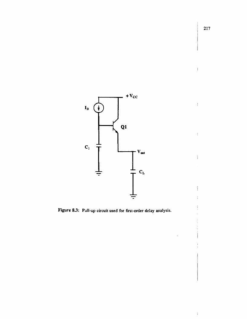
i
Figure 83: Pull-up circuit used for first-order delay analysis.
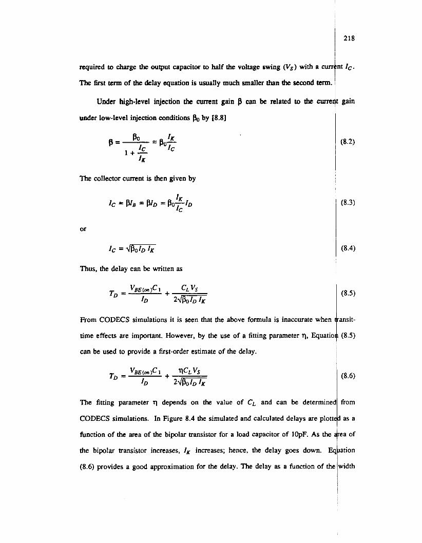
required to charge the output capacitor to half the voltage swing (V,) with a am
The first term of the delay equation is usually much smaller than the seoond term.
Under high-level injection the cumnt gain can be related to the cum:
under low-level injection conditions by (8.81
IK = Po- IC IC
B O
1 + 7 B =
IK
The collector current is then given by
or
IC "457z- Thus, the delay can be written as
From CODECS simulations it is seen that the above formula is inaccurate when
time effects are important. However, by the use of a fitting parameter q, Equatic
can be used to provide a first-order estimate of the delay.
The fitting parameter q depends on the value of CL and can be determine
CODECS simulations. In Figure 8.4 the simulated and calculated delays are plot1
function of the area of the bipolar transistor for a load capacitor of 1OpF. As the
the bipolar transistor increases, IK increases; hence, the delay goes down. E
(8.6) provides a good approximation for the delay. The delay as a function of thc
218
It I C .
gain
(8.2)
(8.3)
(8.4)
(8.5)
ansit-
(8 .5 )
(8.6)
from
I as a
ea of
iation
width
Delay (11s)
6.00
5.50
5.00
4.50
4.00
3.50
3.00
230
2.00
1 .so
1 .oo
0.50
0.00
0.00 20.00 40.00 60.00
Figure 8.4: Simulated and approximated delay as a function of the emitter area of the bipolar aansistor.
I
I
I I
i
I
Ae (bm " 2 ) i
I
i
I
I 1
j 220
of the MOS transistor for a load capacitance of lOpF is shown in Figure 8.5.
approximate delay equation provides a reasonable estimate of the delay. As
Equation (8.6). an increase in W increases Io and the delay goes down.
82.2. Technology and Supply-Voltage Scaling Effects
Simulations have been performed to study the influence of different doping 4ofiles
on the delay of the BiCMOS driver. It should be noted that such simulations
ble only with CODECS and not with a SPICE-like circuit simulator. As poi
Chapter 7, conventional circuit simulation uses analytical models for which, i
is difficult to express the dependencies of model parameters on doping profiles.
The simulated collector Current for the pull-up transient is shown in Fi
a one-dimensional numerical bipolar transistor model with the doping profi
8.7. Initially the current rises rapidly, this rise being determined by 71.
Current level (approximately 2.5mA in this case) the rate of increas
decreases. This takes place when high-level injection occus in the collect0
lar transistor. The base widens, the B of the transistor decreases, and th
increases. As a consequence the current increases at a smaller rate.
From Figure 8.6 and Equation (8.6) it is clear that a high IK is desir
the delay. IK depends on the doping and thickness of the epi layer [
increase in the epi-layer doping or a reduction in the epi-layer thickne
larger IK. It has been shown in Chapter 7 that a transistor with a buri
higher IK compared to one without the buried layer; therefore, a buried 1
for reducing the delay.
In Figure 8.8 simulated collector currents are plotted as a func
transistors with an epi-layer doping of 8 ~ 1 0 ' ~ and a buried layer. The
the transistor, for an epi-layer thickness of 2.1pm, is shown in Figure I
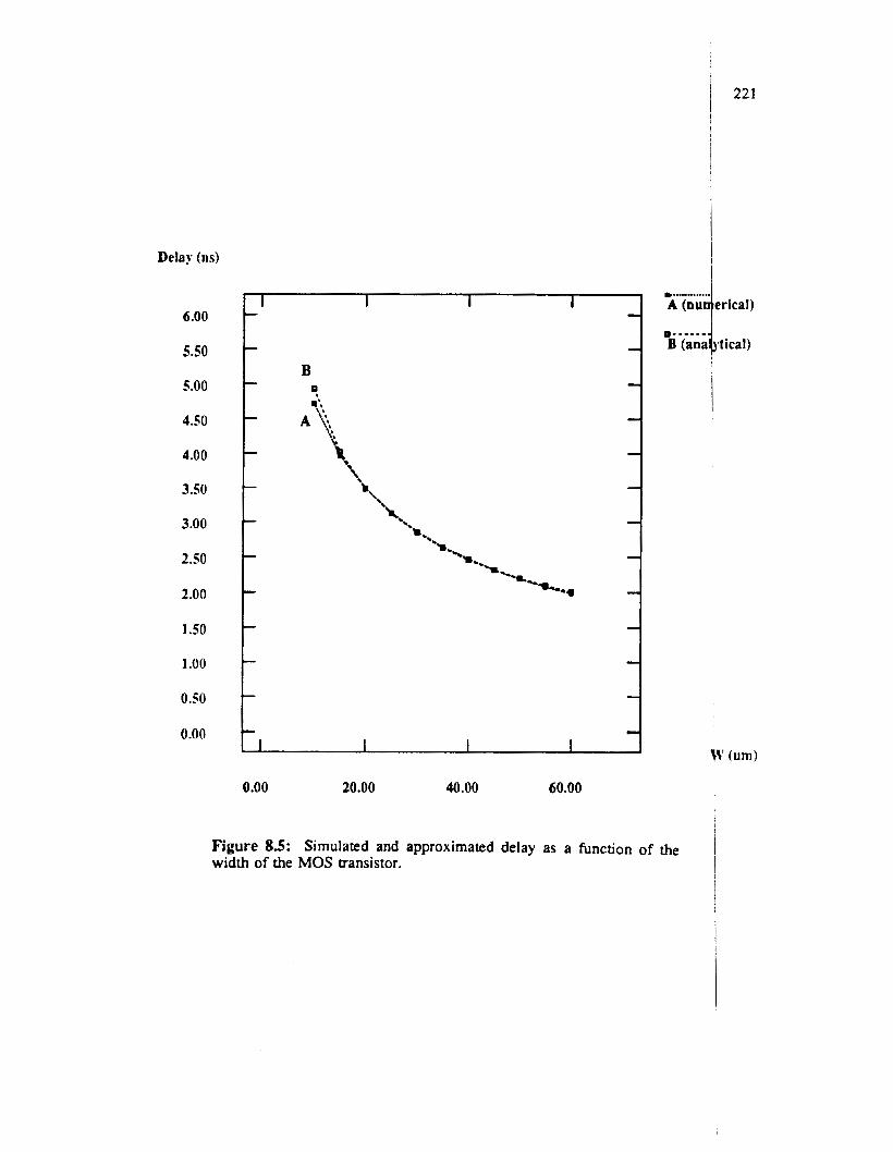
Delay (ns)
6.00
5.50
5.00
4.50
4.00
3.50
3.00
2.50
2.00
1 S O
1 .oo
0.50
0.00
0.00 20.00 40.00 60.00
).--.....
M' (urn)
Figure 8.5: Simulated and approximated delay as a function of the width of the MOS transistor.
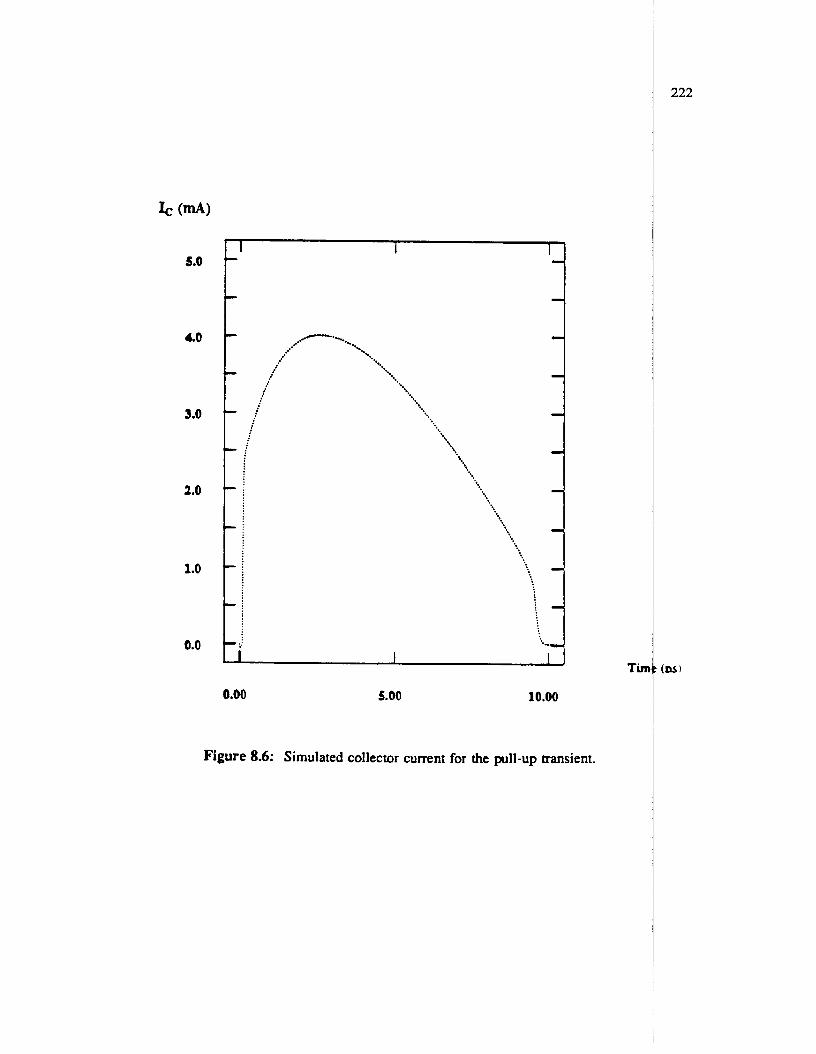
IC
5.0
4.0
3.0
2.0
1.0
0.0 I
L
I
0.00 5.00 10.00
Figure 8.6: Simulated collector current for the pull-up transient.
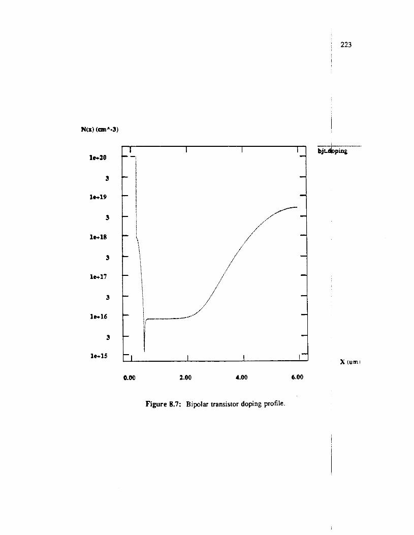
' 223
7 I I 1-20
3
1-19
3
1-16
3
1-17
3
1 ~ 1 6
3
1-15
0.00 2.00 4.00 6.00
Figure 8.7: Bipolar transistor doping profile.
FL-&..." ..........
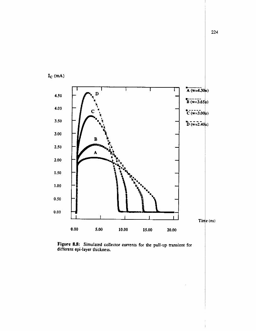
IC (d)
4.50
4.00
3.50
3.00
2.50
2.00
1.50
1 .oo
0.50
0.00 I I 1 I I J
Til
0.00 5.00 10.00 15.00 20.00
Figure 8.8: Simulated collector currents for the pull-up transient for different epi-layer thickness.
225
I thickness is changed by varying the thickness of the buried layer. It is Seen that (a nar-
rower e@ layer results in a larger I,, whereby a larger current is available to
output capacitance, resulting in a smaller delay.
Next consider the delay as a function of the epi-layer doping for the transis@ with
thc doping profile of Figure 8.7. The simulated delay is plotted as a function of thJe load
capacitance and the collector epi-layer doping, ND, in Figure 8.9. Initially an incr ase in
No results in a decrease in the delay. However, for large values of No the ipolar
transistor no longer operates in high-level injection; hence, there is no improve ent in
the delay with an increase in the collector doping (the curves for No of 5x10’ ~ r n - ~
and lxlO” coincide in Figure 8.9). The breakdown of the basecollector jhction
places a limit on the doping used in the collector. An increase in the doping of @e col-
lector also increases the base-collector capacitance. However, t h i s effect is less imE)ortant
since the delay reduces due to an improved high-level-injection behavior of the Uipolar
transistors.
~
The influence of the supply-voltage scaling on the delay of the gate ha$ been
examined in [8.9], and the main conclusions are: for large supply voltages the del4y is a
weak function of the supply voltage. The delay increases as the supply voldge is
reduced for both the pull-up and pull-down transients. However, the pull-downldelay
increases much more rapidly than the pull-up delay at lower voltages since the qBE(on) drop of the bipolar transistor 42, in Figure 8.1, becomes important.
,
83. P-i-n Diode Turn Off
The transient behavior of power devices such as rectifiers, transistors, and
tors in an RLC circuit is an interesting problem. However, adequate analytical
which can accurately describe the complete turn-off process do not exist. Nu
device-level simulations are a useful alternative if the device can be simulated with
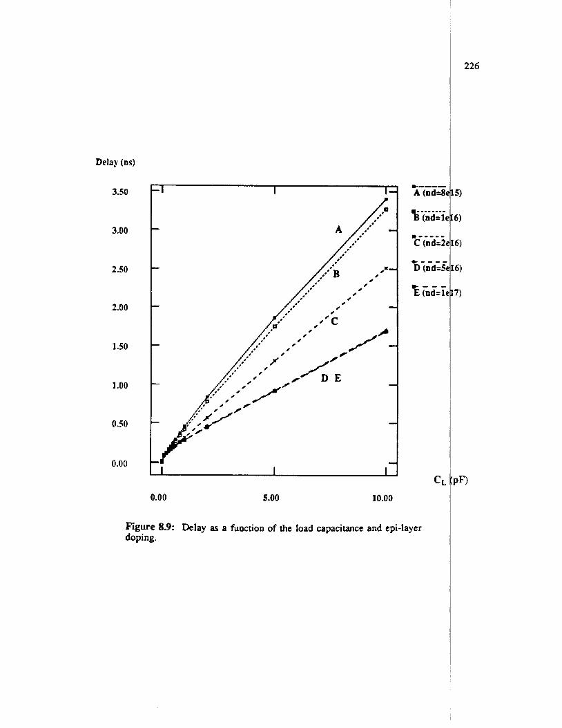
Delay (ns)
3.50
3.00
2.50
2.00
1 S O
1 .oo
0.50
0.00
Figure 8.9: Delay as a function of the load capacitance and epi-layer doping.
227
circuit elements attached to its terminals. Most device simulators r8.10, 8.1 11 only1 allow
voltage or current boundary conditions (some also allow parasitic resistive and cap citive
elements [8.11]), and arc not useful for such simulations. A coupled circuit and bevice c
simulator provides a flexible environment to study the interactions between devi
the circuits in which they are embedded.
83.1. Reverse Recovery of p-i-n Diodes
The reverse recovery of pi-n rectifiers is
iconductor circuits not only because it impacts
an important phenomena in powet sem-
circuit speed, but also because it gffects
power loss and inductive voltage-spike generation. The problem is difficult and andytical
results are available only under special conditions. The reverse recovery with a retiistive
load has been analyzed in r8.121. For practical situations the recovery with a cjurrent
ramp is of interest. This problem has been analyzed for part of the recovery in 18.131,
but a solution is not available for the complete turn-off process. No analytical mOdel is
able to predict the peak reverse voltage that appears across the rectifier during tutn off.
The recovery process is complicated since there is a strong interaction of the (levice
dynamics with the circuit. Device simulation with inductive boundary conditions 1s one
way of analyzing the turn off under special conditions and has been used in [8.14, 8.151.
Consider the simplified circuit of Figure 8.10(a) which is representative of a ppical
turn-off situation. The voltage steps from a positive to a negative value when the (diode
has to be turned OW, the inductor in series models the inductance present in the circuit.
For this example, the p+nn+ diode is modeled as a one-dimensional device with thb uni-
form doping profile shown in Figure 8.10(b). , I
I The simulated current and voltage waveforms for a dlldz of 20 A/ps are shoCn in
Figure 8.1 1. The particular characteristics of these curves can be explained by pbsical
arguments; however, an estimation of the magnitude of the voltage spike is not po
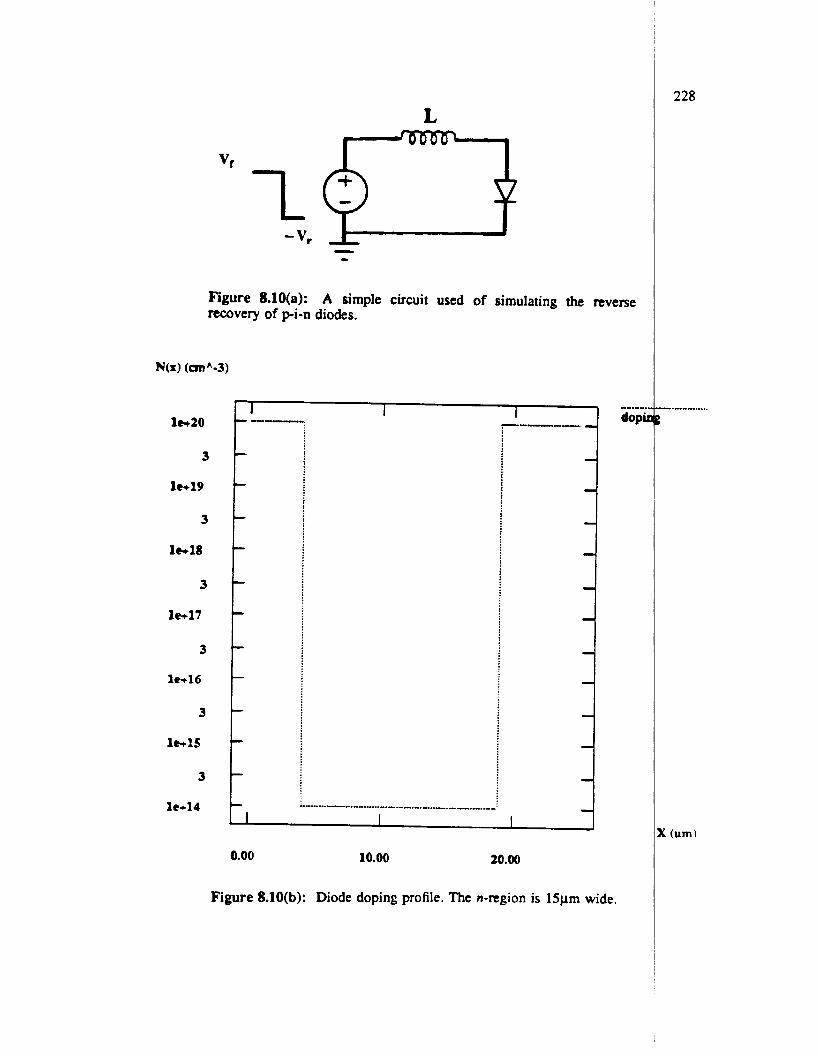
L
Figure 8.10(a): A simple circuit used of simulating the reverse ncovery of p-i-n diodes.
1-20
3
le+19
3
1 ~ 1 8
3
1 ~ 1 7
3
le+16
3
1WlS
3
lt+l4
I I 1
I I
0.00 10.00 20.00
Figure 8.10(b): Diode doping profile. The n-region is 15pm wide.
_".. dopk
228
-." .--......
Y (urn)
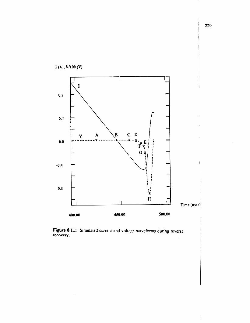
229
I (A), V/lOO (V)
0.8
0.4
0.0
-0.4
-0.8
H I I Time (nsec)
400.00 450.00 500.00
Figure 8.11: Simulated current and voltage waveforms during reverse recovery.
I
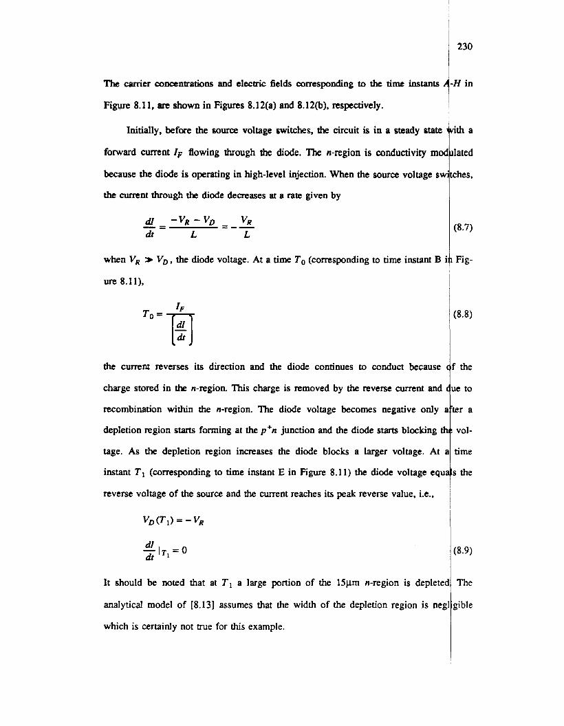
The carrier concentrations and electric fields corresponding to the time instants 1
Figure 8.1 1, are shown in Figures 8.12(a) and 8.12(b), respectively.
Initially, before the source voltage switches, the circuit is in a steady state
forward current 1, flowing through the diode. The n-region is conductivity moc
because the diode is operating in high-level injection. When the source voltage sw
the current through the diode decreases at a rate given by
when VR
ure 8.1 l),
V,, the diode voltage. At a time To (corresponding to time instant B i
the current reverses its direction and the diode continues to conduct because
charge stored in the n-region. This charge is removed by the reverse current and
recombination within the n-region. The diode voltage becomes negative only i
depletion region starts forming at the p+n junction and the diode starts blocking t)
tage. As the depletion region increases the diode blocks a larger voltage. At i
instant Tl (corresponding to time instant E in Figure 8.11) the diode voltage equ;
reverse voltage of the source and the current reaches its peak reverse value, Le.,
q 7 , = o dt
It should be noted that at T1 a large portion of the 1Spm n-region is depletec
analytical model of [8.13] assumes that the width of the depletion region is neg
which is certainly not true for this example.
230
H in
ith a
lated
ches,
(8.7)
Fig-
(8.8)
P the
le to
ter a
vol-
time
s the
(8.9)
The
gible
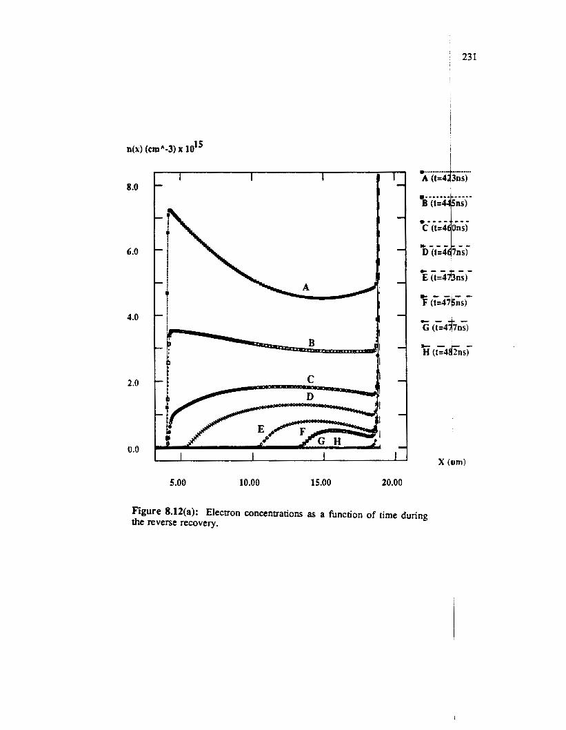
n(r) (~rn~1-3) x 10 15
8.0
6.0
4.0
2.0
0.0
I I I I I 1
t - - E (t=4%&-
I I I I X (ern)
5.00 10.00 15.00 20.00
Figure 8.12(a): Electron concentrations as a function of time during the reverse recovery.
0.0
-2.0
-4.0
-6.0
5.00 10.00 15.00 20.00
Figure 8.12(b): Electric field as a function of time during the reverse recovery.
232
233
tor is essential for estimating the parameters of interest.
The reverse-recovery waveform of the rectifier can also be used to determiie
high-level-injection carrier lifetimes. A charge-control analysis can be used as in
8.171. In [8.16] the device is assumed to be extremely "snappy" and therefo-e
From time T I to Tz (corresponding to the time instant H in Figure 8.11) the I
the
r8.16,
the
current through the diode decreases but is still negative in value, md dlldz > 0.1 As a
result a voltage spike appears across the diode. The diode voltage is related to
dl dz
v, = -v, - t- I (8.10)
This region of operation is hard to analyze since dlldt and, hence, V, are dete ined
by the amount of stored charge remaining within the device. The stored charge turn
depends upon both the circuit and device parameters and its estimation is difficul for a
general situation. As a consequence the peak reverse voltage cannot be determine .
At a time T2 the diode current becomes zero, and may go positive beca se of
oscillations resulting from the Lc circuit formed by the inductance and the depetion-
region capacitance of the diode if sufficient damping is not present in the circuit. I The current waveform during the reverse recovery is idealized to be triandlar in
nature as shown in Figure 8.13. TA and TB, indicated in Figure 8.13, are im@rtant
parameters for the reverse recovery. The sum of TA and TB is the total time f'pr the
reverse recovery and is denoted as Tm. The ratio - is called the softness factott S . A TB T A
large value of S results in a softer recovery and hence a small peak reverse wltage
across the diode. In general, a good rectifier will have a large value of S which ebures
that dlldf is not excessively large during the TB pomon of the reverse rewvery.
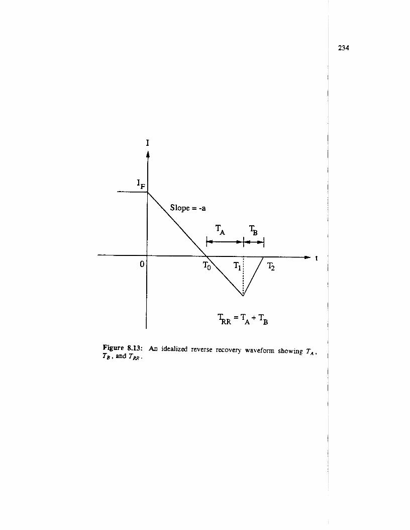
0
I
Slope = -a
TA TB \ k----++
Figure 8.13: A0 idealized reverse recovery waveform showing T A , TB , and Tm .
, 235
I
analysis is not valid for devices with a softer recovery. The analysis of [8.17] i$ more
general; a triangular cumnt waveform is assumed which is representative of a /wider
range of conditions. The procedure for lifetime extraction is verified by sim ations
from CODECS and experimental data in [8.18]. 1
Although the charge-control analysis provides a good estimate for the carri r life-
times from measured characteristics, it cannot be used to provide an a priori estidate of
the softness factor or the magnitude of the voltage spike.
a The factors that affect S can be understood by studying the dependence of $ and
TB on W, the width of the n-region, and ‘5, the high-level-injection canier lifetiqe. In
Figure 8.14(a) simulated TA is plotted as a function of ‘t, with W as a parametet., and
Figure 8.14(b) gives the dependence on W with ‘t as a parameter. The correspclnding
dependencies of TB are shown in Figures 8.15(a) and 8.15(b), respectively. It dan be
seen from Figure 8.14(a) that TA can be fit as TA = k(W)‘t, where k(W) S 1 is al weak
function of W. The dependence of TB on W and ‘t is hard to model analyticall). and,
therefore, simulations are necessary for determining S. The simulated values of E are
shown in Figures 8.16(a) and 8.16(b).
CODECS can also be used to determine the magnitude of the inductive vbltage
spike that appears across the rectifier during the turn off. Simulations have beeb per-
formed for different values of L, and a fixed value of VR=lOV, for two different values
of high-level-injection lifetimes. S and the peak reverse voltage, V p , as a functiod of L
are given in Table 8.1.
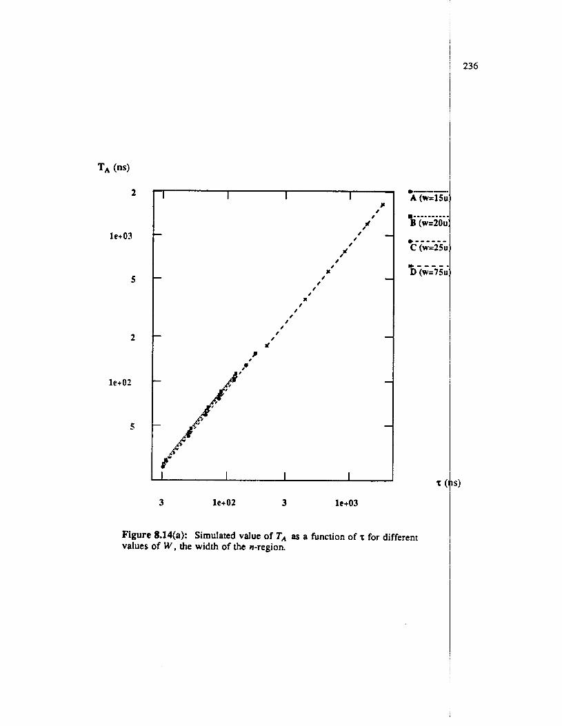
2
le+03
5
2
le+OZ
S
-
J I I 1
3 le+02 3 1e+03
-1 -1
-
P 0 ,*
I 1 1
0 0
1 0
0 0
1 0
0 8
0 0
0 0 s
0 0
0 0
0 0
0 1
Figure 8.14(a): Simulated value of TA as a function of T for different values of W , the width of the n-region.
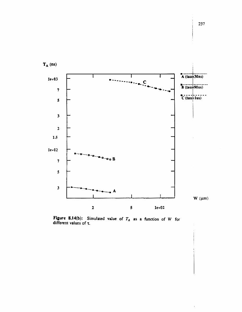
237
TA (ns)
le+03
7
5
3
2
I .S
le+OZ
7
5
3
2 5 le+02
Figure 8.14(b): Simulated value of TA as a function of W for different values of r.
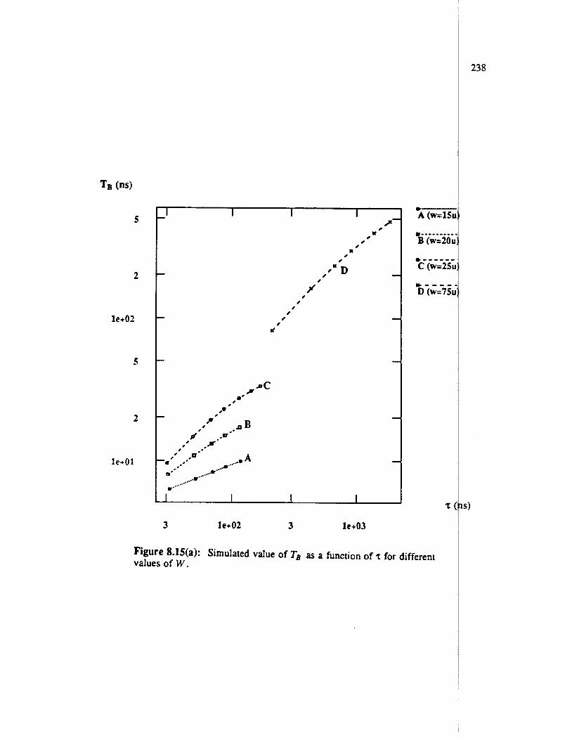
2
le+01
5
2
le+01
3 Ie+02 3 le+03
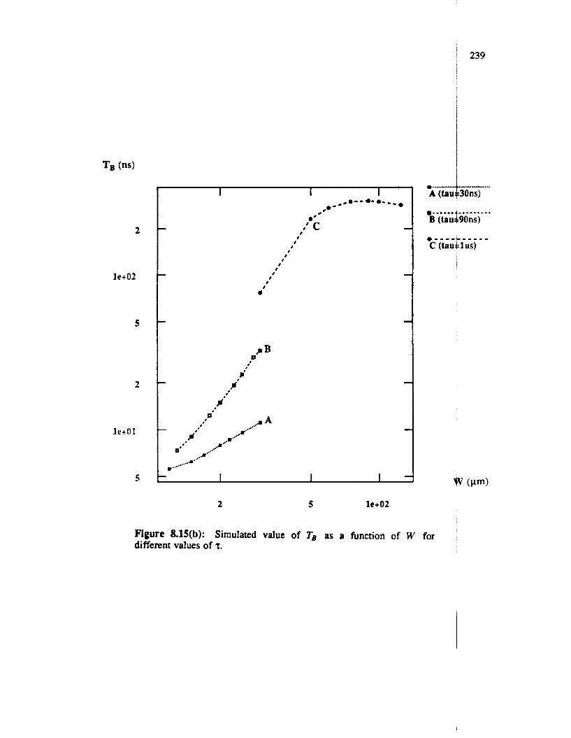
2
le+02
5
2
le+01
5
- - e (. e - - a- e- .* - ** #I c
8 8
0 #
8 #
8 8
8 0
8 0
#
I I I
2 5 le+02
........ ..... *..-- A (tau i 3011s)
Figure 8.15(b): Simulated value of TB as a function of W for different values of 5.
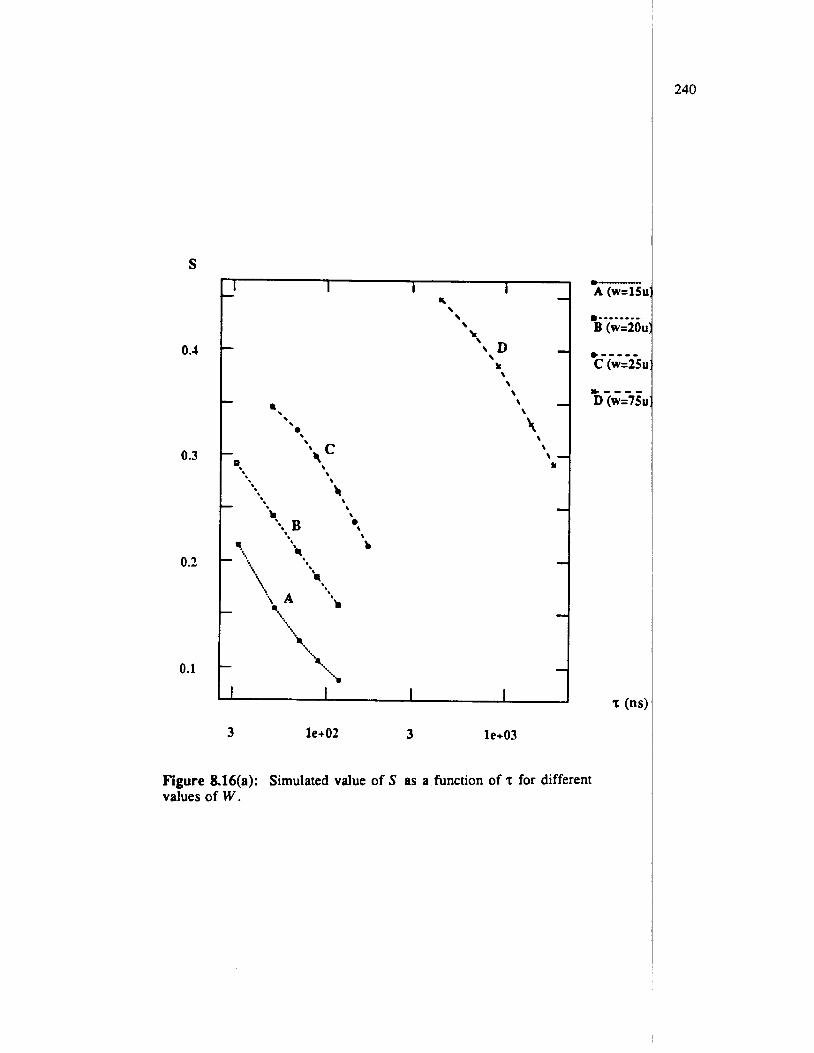
S
0.4
0 -3
0.2
0.1
7 I I I % \ \ \
\ D \\
k \ \ \ \ \
\r \ \ \
I
J I I I
)--.-.-.- A ( ~ = 1 5 ~
s (ns:
3 le+O2 3 le+03
Figure 8.16(a): Simulated value of S as a function of ‘5 for different values of W .
240
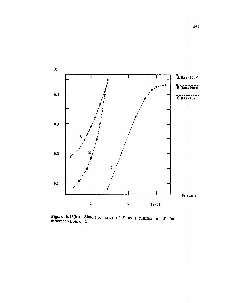
S
0.4
0.3
0.2
0.1
2 5 lc+O2
Figure 8.16(b): Simulated value of S as a function of W for different values of 't.
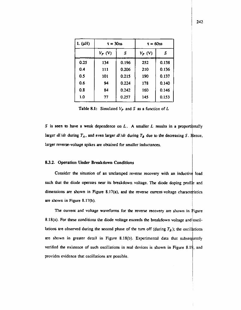
0.25
0.4
0.5
0.6
0.8 1 .o
Table 8.1: Simulated V' and S as a function of L
134 0.196 252 0.138
111 0.206 210 0.136
101 0.215 190 0.137
94 0.224 178 0.140
84 0.242 160 0.146
77 0.257 145 0.153
S is seen to have a weak dependence on L. A smaller L results in a proport
larger d l d r during TA , and even larger d l d r during Ts due to the decreasing S .
larger reverse-voltage spikes are obtained for smaller inductances.
83.2. Operation Under Breakdown Conditions
Consider the situation of an unclamped reverse recovery with an inductiv
such that the diode operates near its breakdown voltage. The diode doping prof
dimensions are shown in Figure 8.17(a), and the reverse current-voltage charact
are shown in Figure 8.17(b).
The current and voltage waveforms for the reverse recovery are shown in
8.18(a). For these conditions the diode voltage exceeds the breakdown voltage anc
lations are observed during the second phase of the turn off (during Ts); the oscil
are shown in greater detail in Figure 8.18(b). Experimental data that subsec
verified the existence of such oscillations in real devices is shown in Figure 8.1
provides evidence that oscillations are possible.
242
lnally
ence,
load
! and
istics
igure
3scil-
itions
ently
, and
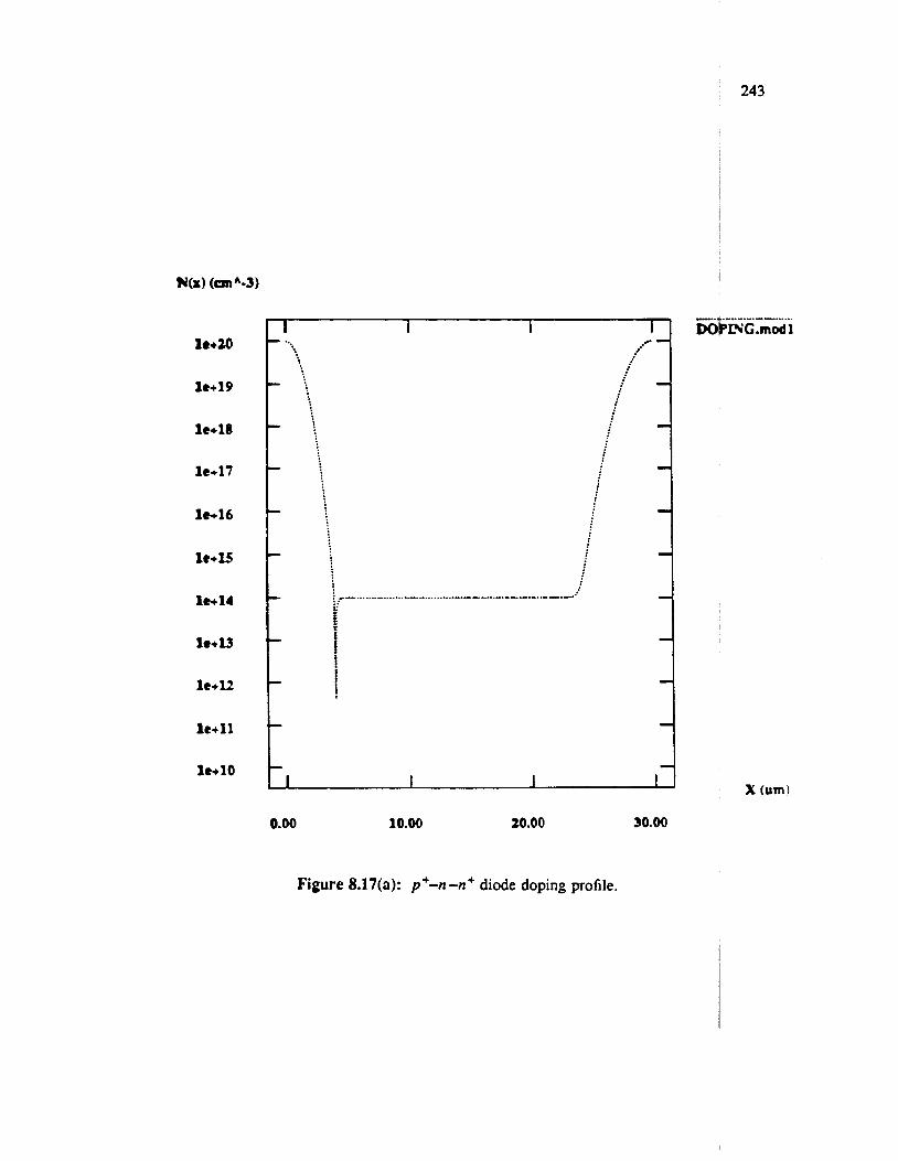
243
1 1 1 1t+20
1t+19
lt+lB
lt+17
1-16
lt+S
lt+14
le+U
le+U
le+ll
le+lO
0.00 10.00 20.00 30.00
Figure 8.17(a): p+-n -n+ diode doping profile.
I
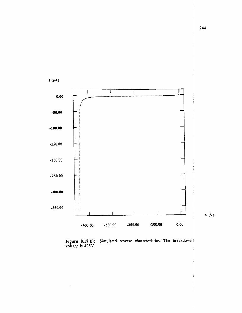
1 (uA)
0.00
-50.00
-100.00
-150.00
.200.00
-250.00
-300.00
-350.00
-ooo.oo -300.00 -200.00 -100.00 0.00
Figure 8.17(b): Simulated reverse characteristics. The breakdown voltage is 425V.
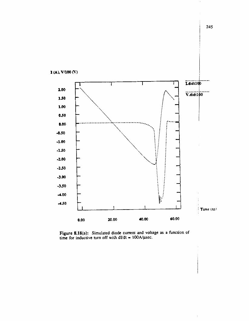
2.00
150
1.00
050
0.00
-050
-1.00
-150
-2.00
-250
-3.00
-350
4.00
-450
20.00 40.00 60.00 0.00
Ldidtl
l i m e
Figure 8.18(a): Simulated diode current and voltage as a function of time for inductive turn off with dYdt = 100Npec.
I
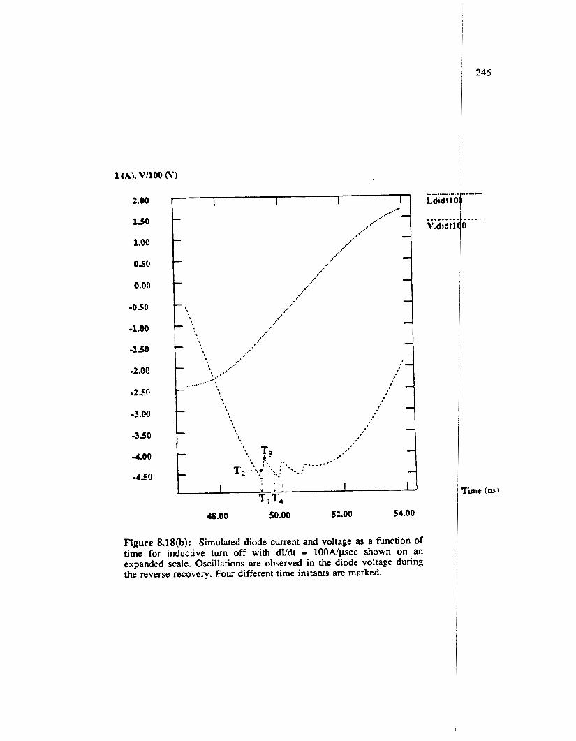
2.60
150
1.00
050
0.00
-050
4.00
-150
-2.00
-250
-3.00
-350
4.00
-4so
Figure 8.18(b): Simulated diode current and voltage as a function of time for inductive turn off with dYdt I: 100Npsec shown on an expanded scale. Oscillations are observed in the diode voltage during the reverse recovery. Four different time instants are marked.
- -..--. ... Ldidtl C
V.didt 1 . . . . . . . .
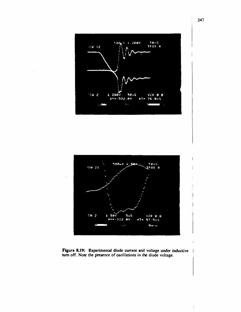
Figure 8.19: Experimental diode ament and voltage under inductive tun off. Note the presence of oscillations in the diode voltage.
247
I
i I I
I
I
1
i
I
i
!
I
I
I
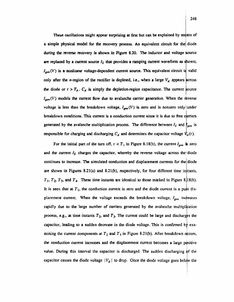
, 248
These oscillations might appear surprising at first but can be explained by
a simple physical model for the recovery process. An equivalent circuit for
during the reverse recovery is shown in Figure 8.20. The inductor and volta
are replaced by a current source Is that provides a ramping current waveform
Ig,,,(V) is a nonlinear voltagedependent current source. This equivalent cir
only after the n-region of the rectifier is depleted, i.e., when a large V,
the diode or t > TA. C, is simply the depletion-region capacitance. The
Ig,,,(V) models the current flow due to avalanche d e r generation. When the
voltage is less than the breakdown voltage, 18,,,(V) is zero and is nonzero
breakdown conditions. This Current is a conduction current since it is due to free
generated by the avalanche multiplication process. The difference between Is
responsible for charghg and discharging C, and determines the capacitor
For the initial part of the turn off, t c T I in Figure 8.18(b), the Current I,,, iif zero
and the current Is charges the capacitor, whereby the reverse voltage across theldiode ~
continues to increase. The simulated conduction and displacement currents for theldiode
are shown in Figures 8.21(a) and 8.21(b), respectively, for four different time i tants,
TI, T2, T3, and Tq. These time instants are identical to those marked in Figure 8 18(b).
It is seen that at TI, the conduction current is zero and the diode current is a p e dis-
placement current. When the voltage exceeds the breakdown voltage, Igcn in eases
rapidly due to the large number of Caniers generated by the avalanche multipl tion
process, e.g., at time instants T2, and T3. The current could be large and dischar s the
capacitor, leading to a sudden decrease in the diode voltage. This is confirmed b I exa-
mining the current components at T2 and T 3 in Figure 8.21(b). After breakdown &curs.
t the conduction current increases and the displacement Current becomes a large
value. During this interval the capacitor is discharged. The sudden
capacitor causes the diode voltage IV, 1 to drop. Once the diode
I
\ !
Figure 820: A physical model to explain the oscillations under inductive turn off of the diode.
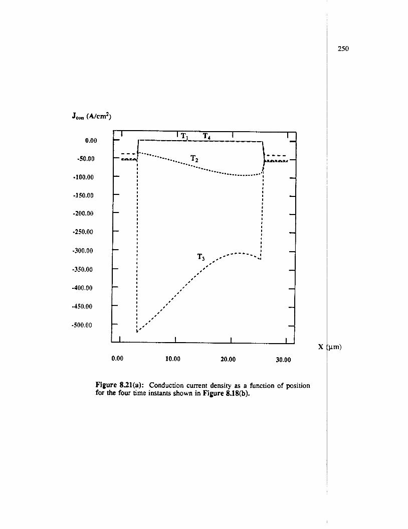
0.00
-50.00
-100.00
-150.00
-200.00
-250.00
-300.00
-350.00
-400.00
-450.00
-500.00
0.00 10.00 20.00 30.00
Figure 831(a): Conduction cument density as a function of position for the four time instants shown in Figure 8.18(b).
x
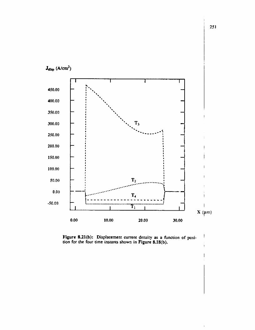
j 251
450.00
400.00
350.00
300.00
250.00
200.00
150.00
100.00
50.00
0.00
-50.00
I I 1 cr I * I I I I - I I I I I I I I I I I I I I - I I I I I I I I I I I I I I I I I I I I I I I
-
-
-
- I I I I I I I I I I I
T, I I
0.00 10.00 20.00 30.00
I
Figure 8.21(b): Displacement current density as a function of p s i - tion for the four time instants shown in Figure 8.18(b).
'
1
I
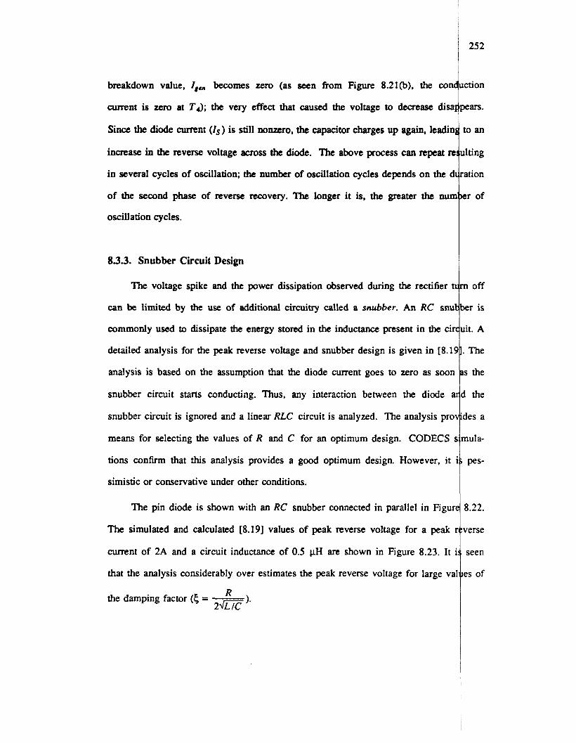
252
I*#,, becomes zero (as seen from Figure 8.21(b), the a n
T4); the very effect that caused the voltage to decrease
breakdown value,
cumnt is zero at
Since the diode current (Is) is still nonzero, the capacitor charges up again, lead
increase in the reverse voltage across the diode. The above process can repeat
in several cycles of oscillation; the number of oscillation cycles depends on the
of the second phase of reverse recovery. The longer it is, the greater the
oscillation cycles.
833. Snubber Circuit Design
The voltage spike and the power dissipation observed during the rectifi
can be limited by the use of additional circuitry called a snubber. An RC
commonly used to dissipate the energy stored in the inductance present in
detailed analysis for the peak reverse voltage and snubber design is given i
analysis is based on the assumption that the diode current goes to zero
snubber circuit starts conducting. Thus, any interaction between the diode
snubber circuit is ignored and a linear RLC circuit is analyzed. The anal
means for selecting the values of R and C for an optimum design. C
tions confirm that this analysis provides a good optimum design. Ho
simistic or conservative under other conditions.
The pin diode is shown with an RC snubber connected in parall
The simulated and calculated [8.19] values of peak reverse voltage
current of 2A and a circuit inductance of 0.5 pH are shown in Fig
that the analysis considerably over estimates the peak reverse voltag
R the damping factor (5 = - 2m ) *
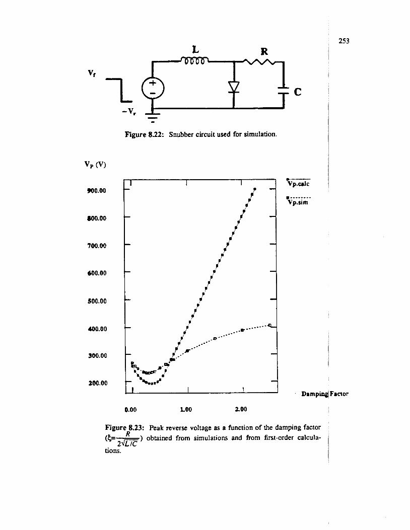
VP (V)
900.00
800.00
700.00
600.00
500.00
100.00
300.00
200.00
L
C
Figure 822: Snubber circuit used for simulation.
1 ). .....--.
I I Vp.crJc c
r' i i i i i i i i i i
8 i i i i i i i - i
i i i i i i i
,F* i
253
1
I
I
I I I I ' Dampmg(Frnor
0.00 LOO 2.00
Figure n 8.23: Peak reverse voltage as a function of the damping factor K <5=- ) obtained from simulations and from first-order calcula-
2m tions. I
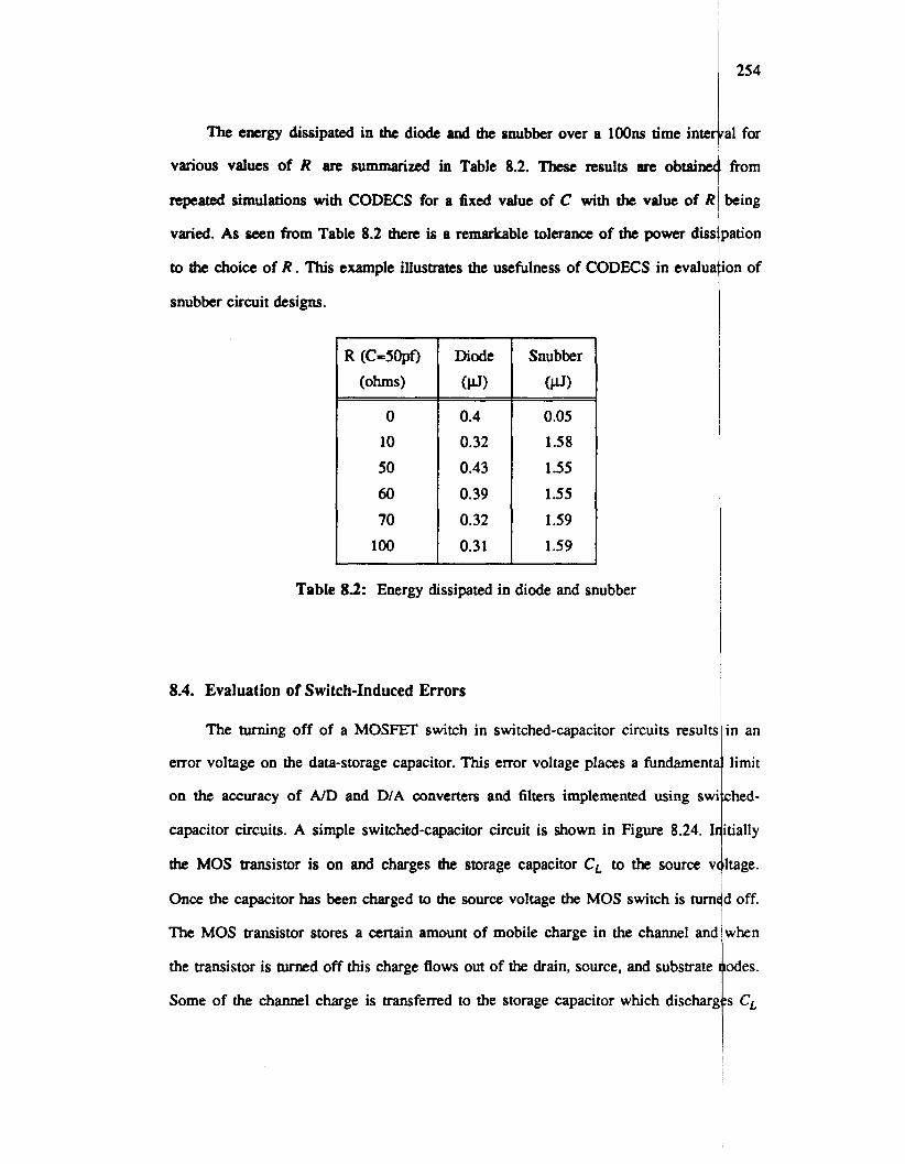
The energy dissipated in the diode and the snubber over a loons time intei
various values of R are summarized in Table 8.2. Thcse results are obtaine
npeated simulations with CODECS for a fixed value of C with the value of R
varied. As seen from Table 8.2 there is a remakable tolerance of the power diss
to the choice of R. This example illustrates the usefulness of CODECS in evaluz
snubber circuit designs.
R (C-SOpf) (ohms)
0 10 50 60 70
100
Diode Snubber
(PJ) (la 0.05 0.4
0.32 1.58 0.43 1.55 0.39 1.55 0.32 1.59 0.3 1 1.59
~
Table 8.2: Energy dissipated in diode and snubber
8.4. Evaluation of Switch-Induced Errors
The turning off of a MOSFET switch in switched-capacitor circuits result!
emor voltage on the data-storage capacitor. This error voltage places a fundament
on the accuracy of A/D and DIA converters and filters implemented using sw
capacitor Circuits. A simple switched-capacitor circuit is shown in Figure 8.24. I
the MOS transistor is on and charges the storage capacitor C, to the source \
Once the capacitor has been charged to the source voltage the MOS switch is furn
The MOS transistor stores a certain amount of mobile charge in the channel anc
the transistor is tumed off this charge flows out of the drain, source, and substrate
Some of the channel charge is transferred to the storage capacitor which dischari
254
a1 for
from
being
)ation
on of
in an
limit
ched-
itially
itage.
d off.
when
,odes.
:s C'
255
and gives rise to an error voltage. Clock-feed-through due to the overlap capaciqces is
another source of error. The error voltage can be reduced by turning off the swi at a
very slow rate but cannot be completely eliminated. T The switch-induced error has been analyzed in [8.20] and a model
obtained for the error voltage with a two-lump approximation. The
error voltage on the gate voltage has been examined under the
This model produces results that are significantly different
nonquasi-static MOSFET model [8.21]. In [8.22] the
include the effect of source resistance and capacitance,
ited to some special cases. An analytical model for
in [8.23] and verified by a numerical solution of
equation However, the model does not include the effect of the driving
impedance. Numerical solution of the onedimensional current-continuity equati
also been used for the turn-off analysis of a MOS pass transistor [8.24]; based on
two-lump model is presented. However, this analysis also assumes a zero gource
impedance. With CODECS it is possible to simulate arbitrary switched-capacitor tircuit
configurations. In particular, the influence of source resistance and capacitance cgn the
error voltage can be determined. In fact, realistic driving sources such as opamps clan be
used for the simulations.
For simulations the MOS transistor geometry and doping are as in Figure'7.18.
The width of the transistor is assumed to be 4pn. For CL of 2pF the ratio of loadlcapa-
citance to the gate capacitance of the MOS pass transistor, CL/C,,, is 242 and th ratio
of the overlap capacitance to the gate capacitance, C,,/C,,, is 0.133. 1 The error voltage at the end of the falling ramp of the gate voltage is
Figure 8.25 as a function of the ramp fall rate for different values of the
The error voltage increases with the fall rate and reaches a maximum. For very hi h fall
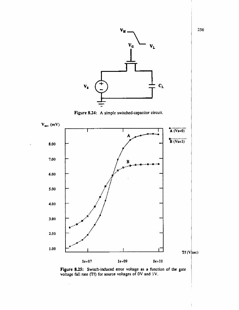
I I VS TI CL
- - Figure 8.24: A simple switched-capacitor circuit.
*.-.."...-.-. A (VS=O)
8.00
7.00
6.00
5.00
4.00
3.00
2.00
1 .oo Tf (7
le+07 le+09 l e + l l
Figure 8.25: Switch-induced error voltage as a function of the gate voltage fall rate (To for source voltages of OV and 1V.
257
rates the error voltage drops due to nonquasi-static operation.
Next consider the influence of source resistance, Rs, on the error voltage The
source voltage, are presented in Figure 8.26. It is seen that the switch error in eases
with an increase in the source resistance. This is to be expected, since a larger amo nt of
channel charge flows into the storage capacitor than into the source. The source ~ sis-
simulated emr voltages as a function of Rs, and the gate voltage fall rates, for
tam rcsmcts the flow of charge to the voltage source. The error voltage also indeases
with an increase in the fall rate initially, but decreases at high fall rates.
The effect of source capacitance, Cs, is shown in Figure 8.27. The error voltage is
plotted as a function of Cs for different fall rates, Vs = 0, and Rs = 10K. The sburce
capacitance has negligible effect at very small and very large fall rates. Howev+, for
values of fall rate in between the two extremes the error voltage decreases 4s Cs
increases.
Next the circuit shown in Figure 8.28 is considered. The error voltage for different
circuit configurations is plotted as a function of the fall rate of the gate voltage in €figure
8.29. The different configurations are
(i) Cs = 0, Rs = 1OK and no M2,
(ii) Cs = 2pF, Rs = 10K and no M2,
(iii) Cs = OpF, Rs = 10K and M 2 as shown (dummy technique), and
(iv) Cs = 2pF, Rs = 10K and M 2 as shown (balanced technique).
Thus, various techniques for error cancellation such as the dummy technique r8.2:
the balanced technique r8.261 can be evaluated. It is seen from Figure 8.29 that th
anced technique is most effective in reducing the switch-induced error voltage.
1 and
! bal-
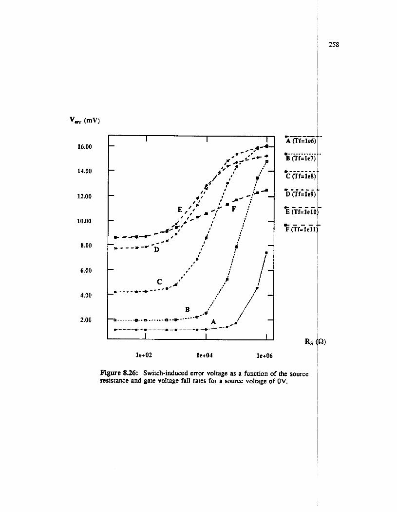
verr (mv)
16.00
14.00
12.00
10.00
8.00
6.00
4.00
2.00
I
F : L , . I
, #
L . i I . , #
I I
, , , , , , ./
.-d / B / A p .----- *-.a *-.e------= -
e ....... -.-*.-.* ............. *, ...a ....._....- * .... e .....*"------*a
).-.-- A (Tf=l&:
R S
le+02 1e+01 le+06
Figure 8.26: Switch-induced emor voltage as a function of the source resistance and gate voltage fall rates for a source voltage of OV.
258
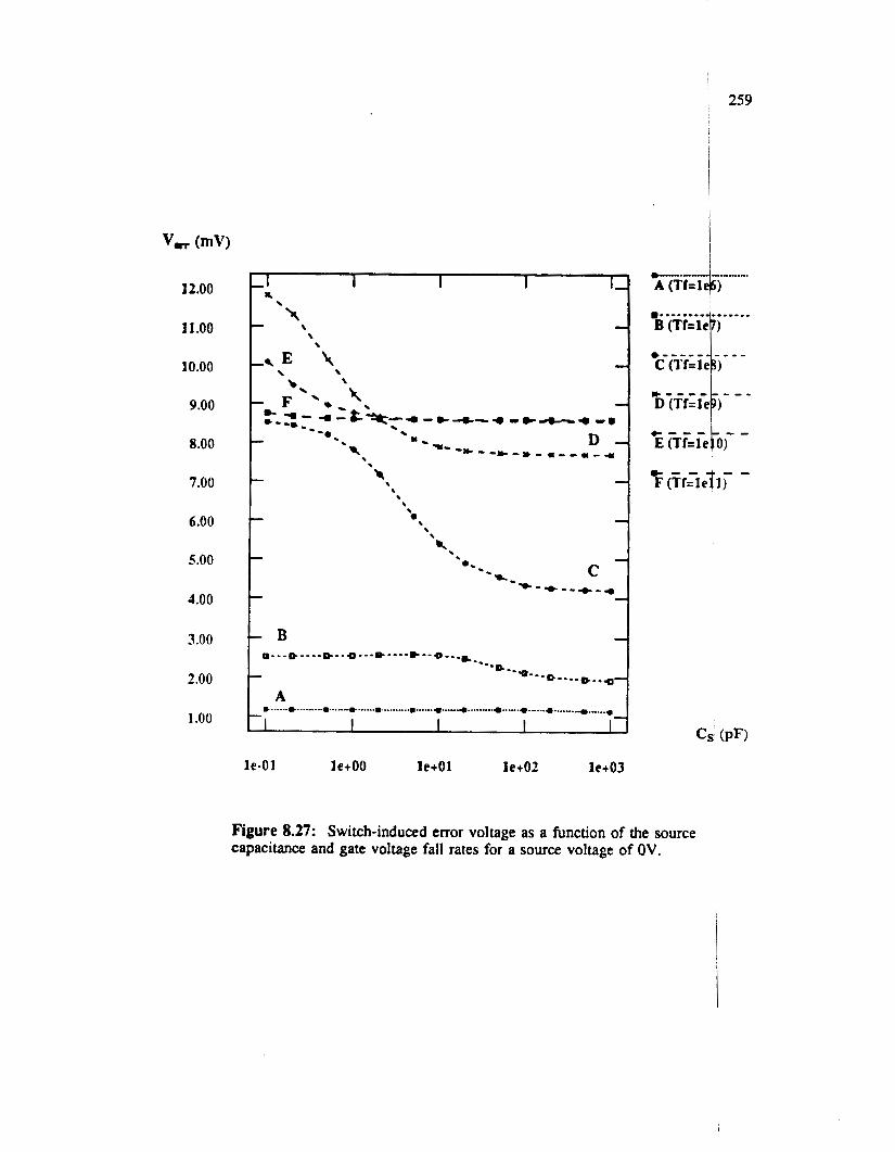
' 259
I 12.00
11 .oo
10.00
9.00
8.00
7.00
6.00
5.00
4.00
3.00
2.00
1 .oo
le+00 1e+01 le+O2 1e+03 le-01
Figure 8.27: Switch-induced error voltage as a function of the source capacitance and gate voltage fall rates for a source voltage of OV.
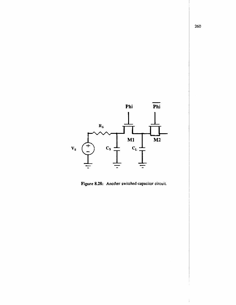
Phi Phi
Figure 8.28: Another switched-capacitor circuit.
260
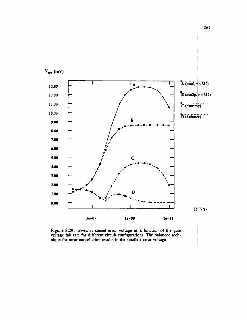
v, (mV>
13.00
12.00
11.00
10.00
9.00
8.00
7.00
6.00
5.00
4.00
3.00
2.00
1 .oo 0.00
le+07 le+09 l e+ l l
*..-....-..- A (cs=O, I
261
”.......... oM2)
no M2)
Y)
------
.---
Figure 8.29: Switch-induced error voltage as a function of the gate voltage fall rate for different circuit configurations. The balanced tech- nique for error cancellation results in the smallest error voltage.
85. Evaluation of Analytical Models
This section illustrates the application of CODECS for verification of am
models. CODECS provides a capability to evaluate analytical models, and to sef
analytical model properly incorporates the physical operation of the device.
As a first example CODECS is used as a device simulator. An analytical mor
the lateral eltctric field in lightly doped drain MOSFETs has been derived u
quasi-twodimensional analysis [8.27]. Simulations from CODECS are used to ver
model. The elecoic fields obtained from the analytical model, for the full-overl:
non-overlap devices are plotted in Figures 8.30 and 8.31, respectively. Results o
dimensional CODECS simulations for the same device and bias conditions ar
included in these figures. The analytical model shows good physical agreement w
numerical simulations.
The second example concerns the turn-on and turn-off transients of a MOSI
illustrated in Chapter 7. In Figure 8.32 are plotted the simulated drain and
currents for the turn-on transient. Figure 8.33 gives the corresponding results 1
turn-off transient. The simulated results are from CODECS and the nonquas
model of Park t8.281. The analytical model predicts that the currents cannot I
instantaneously and the nature of the simulated waveforms is similar to that 01
from CODECS. The steady-state values of the currents for the turn on are di
because of the differences in the dc characteristics of the numerical and ani
models It can, therefore, be concluded that the model of [8.28] properly simulate
quasi-static operation.
262
ytical
if an
el for
ing a
y the
3 and
two-
also
5 the
2T as
ource
)r the
static
iange
ained
ferent
ytical
non-

000
000s
00'00 I
OO'OSI
00'002
OO'OST
OO'OOC
OO'OSC
00'00P
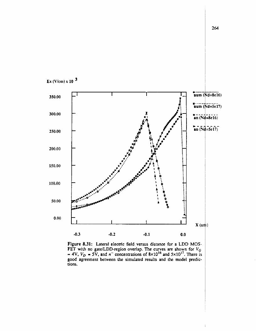
350.00
300.00
250.00
200.00
150.00
100.00
50.00
0.00 i I
J I I I
-0.3 -0.2 -0.1 0.0
Figure 8.31: Lateral electric field versus distance for a LDD MOS- FET with no gate/LDD-region overlap. The curves are shown for V , = 4V, V, = SV, and n- concentrations of 8 ~ 1 0 ’ ~ and 5x10”. There is good agreement between the simulated results and the model predic- tions.
264
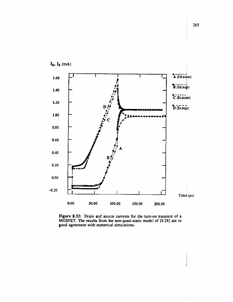
265 I I
1.60
1.40
1.20
1 .oo
0.80
0.60
0.40
0.20
0.00
-0.20
0.00 50.00 100.00 150.00 200.00
Figure 8.32: Drain and source currents for the turn-on transient of a MOSFET. The results from the non-quasi-static model of [8.28] are in good agreement with numerical simulations.
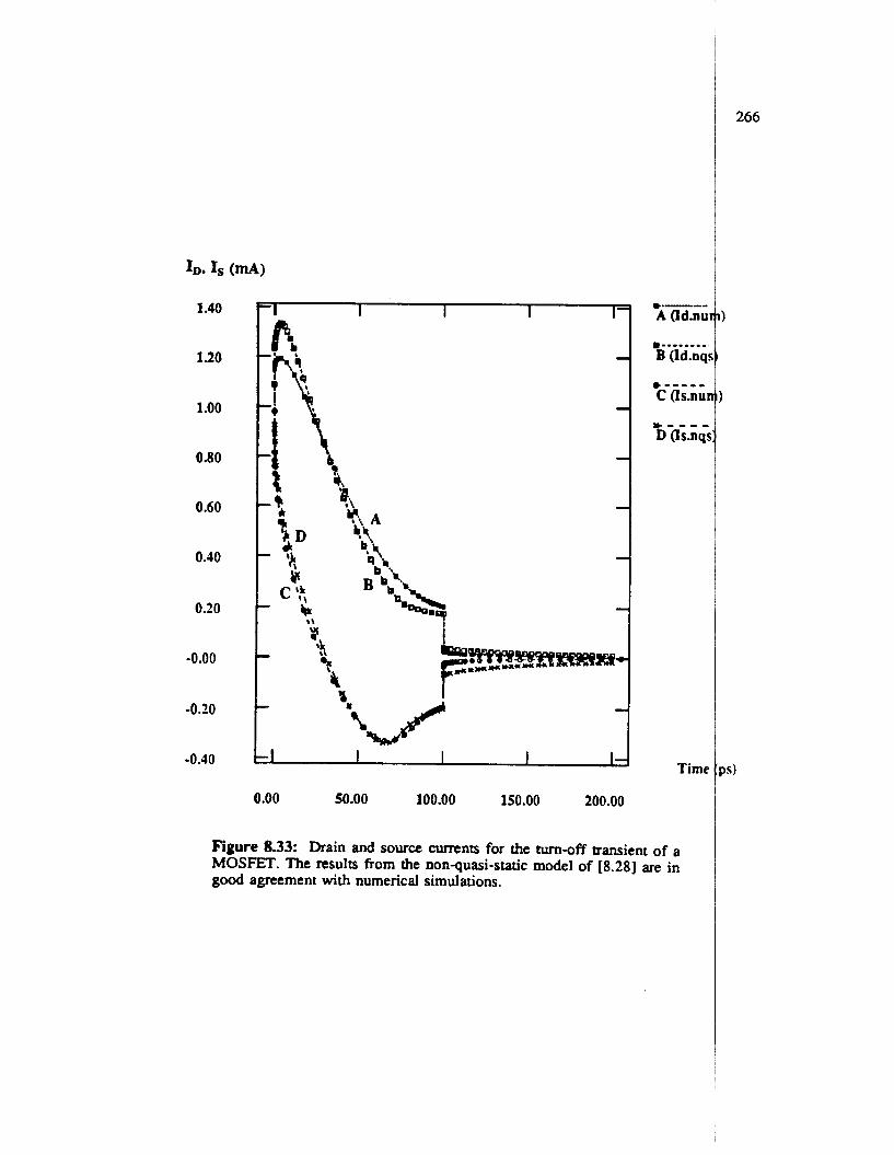
1.40
1.20
1.00
0.80
0.60
0.40
0.20
-0.00
-0.20
-0.40 I I I I -
0.00 50.00 100.00 150.00 200.00
Figure 8.33: Drain and source currents for the turn-off transient of a MOSFET. The results from the nonquasi-static model of [8.28] are in good agreement with numerical simulations.
267
CHAPTER 9
Conclusions
I Usually circuit simulators make use of analytical models for semiconducto dev-
ices. These models are derived from the basic physical laws governing device o ration
under simplifying assumptions. Empirical factors are introduced such that a good t can
be obtained with measured data from fabricated devices. Parameter-extraction pr ams
are used to obtain the model parameters for a device model from experimentally i eas-
ured data. These models cannot predict the effect of changes in process technolo& and
device design on circuit performance. Repeated fabrication of devices and circuid is an
expensive and time consuming way to make such evaluations. 1
1
Device simulations can be used to predict the effect of technology changes 04 dev-
ice performance. This information could be used with a circuit simulator to predibt cir-
cuit performance. However, the use of curve fitting to obtain the model paramet ei rs for
the analytical models, from the simulated current-voltage characteristics, results in a
loose coupling between the device simulator and the circuit simulator. Such an apdroach
may not provide adequate information for a predictive analysis. I
A coupled device and circuit simulator is a general solution to the modeling!prob-
lem. Detailed information from the device-level simulations can be used at the eircuit
level. It provides a direct link between technology and circuit performance and dan be
used to evaluate the impact of alternate processes and device designs on circuit
mance. In addition, such a simulator extends the capabilities of a device simulator
devices can be simulated with circuit embedding. Present day device

only voltage or current boundary conditions and resistive or capacitive elements at the
terminals; therefore, they cannot be used to simulate realistic boundary conditio . In L. practice the device is embedded in a circuit and a mixed-level circuit and device
tor can be used to study its performance with circuit boundary conditions.
The accuracy of analytical models used for circuit simulation can also be
by mixed-level circuit and device simulations. If some important physical
ignored in the analytical model, then the model has to be modified to
effects. Using coupled simulations, one can also identify circuit
This dissertation presents a general framework for
simulation. The goal has been to implement frequently
with a wide variety of numerical models. A new
program, CODECS, has been developed as part
for the circuit-simulation capability and for
The coupling techniques are general and
analytical models are essential.
new one- and two-dimensional device simulator has been developed that suppor's
transient, small-signal ac, pole-zero, and sensitivity analyses at the device level. Th
ice simulator provides a comprehensive set of analyses capabilities that are not
with any existing device-simulation programs.
Various algorithms to couple the device and circuit simulators for dc and
analyses have been implemented in CODECS. These algorithms are evaluated based
their convergence properties and runtime performance. This study provides guidelines
choice of a particular coupling algorithm. A modified two-level Newton algoritim
used for dc analysis whereas a full-block-LU decomposition algorithm is used for
sient analysis. This combination of algorithms provides reasonable convergence a n c
time performance. Coupling for small-signal ac and pole-zero analyses is also described.
dc,
! dev-
available
tralsient
on
for
is
tran-
run-
269
Dc convergence is a serious problem in coupled circuit and device simulatiob. The
device-level equations are highly nonlinear and iterative methods fail to converg to a
solution if the terminal voltages change by a large amount. Heuristics have been i vesti-
gated to improve convergence for dc analysis. Some of the techniques used
method, and a backtracking scheme if convergence is not achieved for a particul bias
point. The limiting sckmes may be conservative but are justified since dc analy s is a
very small fraction of a complete transient simulation. Schemes for timeste r: and
modified two-level Newton algorithm with device-based limiting, a damped-
integration-order control in transient analysis are also described. CODECS uses th local
error estimates for automatic control of timesteps and integration order. Latencyicheck
is extremely important for mixed-level circuit and device simulation since evalua 'on of
numerical models is computationally expensive. A scheme for device bypass is pre ented
and evaluated. The implementation of small-signal ac and pole-zero analyses, and c and
transient sensitivity computations at the device level are also described.
t
Q
F I 0
I
Analytical models are compared with numerical models to indicate their
weaknesses under various regions of device operation. Since numerical models are I based
on physics they provide more reliable results and a means for identifying the shoqcom-
ings of analytical models. It is shown that even if the model parameters are ex acted
such that there is a good agreement with the dc characteristics obtained experime tally,
the transient response may be significantly different. A good dc model does not
tee accurate transient operation. The speed-performance comparison indicates the qost of
using numerical models instead of analytical models. However, some applicatio well
justify the computational costs to obtain physically meaninghl simulation results.
I
T P
Taran- I
1 Applications have been used to illustrate the advantages of mixed-level circ4t and
device simulation. These examples again provide evidence that analytical models b e of
limited utility in some applications. Typical examples are high-level-injection effe/cts in
270
current-continuity equations would provide a significant improvement in
diodes and bipolar transistors, high-frequency or nonquasi-static operation of 6e c con-
ductor devices, charge distribution during the turn off of an MOS 8witch in/ MOS
switched-capacitor circuits, and simulation of power devices. The last application s par-
ticularly suited to mixed-level circuit and device simulation, since most power ' cuits
employ a small number of power devices for which accurate models are necess ; the
CODECS has also been used as a vehicle to study the performance of Lisp based
mixed-level circuit and device simulation. An initial prototype for CODEC I was
rest of the circuit can be simulated with analytical models.
developed in Lisp using object-oriented programming on the Symbolics 360 Lisp
machine. Although Lisp provided an environment for rapid prototyping, the Lisp based e
speed
simulator was extremely slow to be suitable for practical applications. Detailed
profiles are presented to identify the portions where the program spends
time. Comparisons are provided with the new version of CODECS in the
ming language. I
Future research should focus on speeding up the mixed-level circuit and /levice
simulator. This can be achieved by the use of vector or multiprocessing com uters.
Parallel model evaluation [9.1] in a mixed-level circuit and device simulator shoul ! pro-
vi& an almost linear speedup with the number of processors. Loosely coupled
cessors may be quite suited since the time required for model
27 1
performance. 1 I
A mixed-level circuit and device simulator is only as good as the physical &dels
used at the device-simulation level. CODECS currently uses physical models thatlhave
been widely accepted in the litera-. These models should be updated as better +dels
become available. In addition, the device-simulation capability should be tuned to 4 pro-
cess line and the models verified with actual measurements. This will provide a basis for
comparing experimentally fabricated circuits and simulated results.
Additional analysis capabilities need to be implemented at the device-simuiation
level. These include the use of numerical models for noise calculations. Numerical Itech-
niques have been used for calculating the low-frequency noise of MOSFET’s in r9.41.
To be useful for power device designers CODECS should also allow the simulation
of thyristor circuits. This can be achieved by implementing current boundary conditions
at the device-simulation level. Temperature gradients are important in power detices.
Consequently, the heat-flow equation must be solved coupled with the Poisson’s 4 the
current-continuity equations. Some device simulators allow non-isothermal simula(tions
19.71, and such a capability will be extremely beneficial in CODECS.
As devices are scaled down three-dimensional effects become important. Mddern
IC fabrication processes may dictate the use of three-dimensional numerical model$ in a
mixed-level circuit and device-simulation environment. The coupling techniques used in
CODECS can be extended to three-dimensional numerical devices. However, compta-
tional costs are going to be of serious concern and multiprocessors should be bsed.
Mixed-level circuit and device simulations could be extremely useful for future e e e -
dimensional or multi-layer technologies. I
i At present CODECS works for rectangular geometry silicon devices. The
capabilities of CODECS should be enhanced to other materials such as
heterosbucture semiconductor devices. CODECS should also be extended

generalized geometries; this could be done by use of triangular grids as in
A mixed-level circuit and device simulator provides an environment
useful to ~ ~ O C C S S , device and circuit designers. Process designers could
coupled with a proass simulator to design a high-perfoxmance
desired set of specifications for a given circuit design. This
custom IC process. Device designers can evaluate
impact on circuit performance. Circuit designers
greater accuracy is desired for simulations as
performance circuits.
27 3
APPENDIX A
CODECS User’s Guide
A.l. Introduction
CODECS is a coupled device and circuit simulator that allows accurate and
detailed simulation of semiconductor circuits. The simulation environment of COOECS
enables one to model critical devices within a circuit by physical (numerical) qodels
based upon the solution of Poisson’s equation and the current-continuity equ4tions.
Analytical models can be used for the noncritical devices. CODECS incowrates
SPICE3 for the circuit-simulation capability and for analytical models of semiconluctor
devices. Numerical models are provided by a new one- and two-dimensional evice
simulator. Dc, transient, and small-signal ac and polehero analyses can be perfoled on
circuits containing one and two-dimensional numerical models. The numerical moQels in
CODECS include physical effects such as bandgap narrowing, Shockley-Hall-Redd and
Auger recombinations, concentration- and field-dependent mobilities, concenqation-
B
dependent lifetimes, and avalanche generation.
The input format is similar to that of SPICE3. All circuit elements and analytical
semiconductor device models can be used as described in the SPICE3 User’s Guiide. A
description of the numerical models of CODECS is provided here.
A.2. Circuit Description
The circuit description can be entered in a manner similar to that of SPICE
cuit element description lines contain the element name, the circuit nodes to whit
connected, and the values of the parameters that determine the electrical charam
of that element. A numerical diode name must begin with the letter A, a numeric
name must begin with the letter B, and a numerical MOSFET with the letter N.
Data fields that are enclosed in ‘c >’ in the description below are optional.
A.3. Element Descriptions
A3.1. Numerical Diodes
General form:
AXXXXXXX N+ N- MN IE <AREA 7 4 Jb <WIDTI
N+ and N- are the positive and negative nodes, respectively.
, U b
h4NAME
model name. AREA is the area for a one-dimensional diode in cm2. WIDTH
width of a two-dimensional diode in cm. The default values of AREA and WID:
lcm2 and lcm , respectively, and are used when these parameters are not specified.
Examples:
ACLAMP 1 2 AREAZlU
ACLAMP 1 2 WIDTH=lE-2
274
. cir-
I it is
istics
I BJT
s the
s the
H are
A33. Numerical Bipolar Junction Transistors
General form:
BXXXXXXX NC NB NE MNAME <AREA VALUE> <WIDTH V A L W
NC, NB, and NE arc the collector, base, and emitter nodes, respectively. Itdl
is the model name. AREA is the area for a one-dimensional BIT in cm2. WIDTH
width of a two-dimensional BJT in cm. The default values of AREA and WIM
lcm' and lcm , respectively, and are used when these parameters are not specified.
Examples:
BINV 1 2 0 AREA-1E-6
BINV 1 2 0 WIDTH=lE-2
A.33. Numerical MOSFETs
275
4ME
s the
1 are
General form: I
NxXXXXXX ND NG NS NB MNAME <WIDTH VALUE>
ND, NG, NS, and NB are the drain, gate, source, and bulk (substrate) iodes, I
respectively. MNAME is the model name. WIDTH is the width of the two-dimenbional
MOSFET structure in cm. The default value of the width is lcm , and is used when the
WIDTH parameter is not specified in the input. i
Examples :
MPULLDN VOUT VIN 0 0 ENH WIDTH=20E-4
MPASS 2 4 10 0 ENH WIDTH-1M
A.4. Model Descriptions
The numerical semiconductor device models are specified using the .MODEL
mand similar to that used for the analytical models in sPICE3.
General form:
.MODEL MNAME TYPE PNAMEl PVALl PNAh4E2 PVAL2 ... MNAME is the model name. TYPE is NUMD for a numerical diode model,
for a numerical BJT model, and N M O S for a numerical MOSFET model. The F
eters can be single valued, vector valued, or logical flags. Onedimensional and
dimensional numerical models differ in their input parameters. A description
model parameters is given below. First the common model parameters that mod
various physical effects are described. This is followed by a description of the
parameters for one-dimensional models and two-dimensional models, respectively.
A.4.1. Parameters for Physical Effects
CODECS includes several physical effects which can be included in a simu
by specifying the corresponding parameters. The model parameters are
AS. Model Parameters for One-Dimensional Numerical models
The parameters described in this section are used to define the mesh for
discretization, the doping profiles, and the material regions for the device.
A S S . Mesh Description
The mesh for a onedimensional device is specified by the MESH model pa
ter.
General form:
276
mom-
n3J-r
ram-
two-
f the
1 the
iodel
ation
pace
une-
name
located at X = O p m . The 11th mesh point is at X = lpm, and the 51st mesh point
X = 2p.m. Thus, ten mesh points are uniformly placed in the interval (0, lpm ) and
mesh points are uniformly placed in the interval (Ipm , 2p.m). The mesh spacing ir;
form within an interval but nonuniform from interval to interval.
SRH AUGER BGNW C O N n A U CONCMOB FIELDMOB AVAL.
NBGN
is at
forty
uni-
T N O TPO MUNO MUPO MOBMODEL
parameter
Shoclrley-Read-Hall recombination
Auger recombination
bandgap narrowing concentrationdependent lifetimes concentrationdependent mobility field-dependent mobility avalanche generation
reference concentration for bandgap narrowing model
low doping electron lifetime
low doping hole lifetime low doping, low field electron mobility low doping, low field hole mobility mobility model
default
not included
not included not included not included not included not included not included 1x10'~ cmv3
20 ILF 20 ILF
1400 cm2/V-s
480 cm2iV-s
277
i
I
I I !
I
I Scharfetter-Gum el 4
MESH MESHNO XPOS
XPOS is the X position, in pm, of the mesh point specified by MESHNOl The
mesh parameter can be used any number of times to generate a nonuniform grid.
Example:
MESH 1 0 MESH 11 1 MESH 51 2
A5.2. Doping Description
The doping profile for the device is specified by analytical formulas. The a
profile types am uniform, Gaussian, exponential, or crror function The general fc
each of these profiles is as follows.
A53.1. Uniform Doping Profile
General form:
UNIF CONC XLO XHI
UNTF specifies a uniform doping profile between XLO and XHI. Both XL
A negative value is sp XHI are given in cm. CONC is the doping level in
for a p-type material and a positive value for an n-type material.
The doping N ( x ) is calculated using the following expression,
0 x <xu)
x > X H I N ( x ) = {y XLO 5 x S X H I
Examples:
UNIF 1E15 0 1E-4
This defines a n-type uniform doping of 1 x 10'' for the interval (0, lp
UNIF -1E16 0 5E-4
This defines a p-type uniform doping of 1 x 10l6 for the interval (0, 5p
27 8
3wed
m of
1 and
:ified
1.
1.
279
A.5.2.2. Gaussian Implantation Profile
General form: I I ~ GIMP CONC CHAR XPOS
GIMP specifies a Gaussian implantation profile with a peak concentration dONC
in ~ r n - ~ , a characteristic length of CHAR in cm, end tfre peak is located at @S in
cm . CONC is a negative value for a p-type material. The doping N ( x ) is calculated! as
N ( x ) = CONC xexp [- [ x -XPOS r] CHAR
Examples:
GIMP 5E18 1.35E-4 6E-4
This defines a n-type Gaussian profile of peak concentration 5 x 10l8 c&, a
characteristic length of 1.35 p n , with the peak of the profile placed at 6 p .
GIMP -1E19 0.15E-4 0
This defines a p-type Gaussian profile of peak concentration 1 x 10¹⁹ ~ m - ~ , cqarac-
teristic length of 0. IS pm, with the peak of the profile at the origin.
A.523. Exponential Doping Profile
General form: I
EXP CONC CHAR X P O S
EXP specifies an exponential profile with a peak concentration CONC in cr4-3, a
characteristic length of CHAR in cm, and the peak is located at XPOS in cm. CO&C is
a negative value for a p-type material. The doping N ( x ) is calculated as I
XPOS - - x I 1- ' CHAR N ( x ) = CONC x exp

Example:
EXP 5E18 1.35E-4 6E-4
This defines a "-type! exponential doping profile of peak concen
5 X 10" ~ r n - ~ , a characteristic length of 1.35 p n , with the peak of the profile pli
4w.
A.52.4. Error-Function Doping Profile
General form:
ERFC CONC CHAR XPOS
ERFC specifies an error-function profile with a peak concentration CONC in
a characteristic length of CHAR in cm , and the peak is located at XPOS in cm. 1
is a negative value for a p-type material. The doping N ( x ) is calculated as
['x:iix' 1 N ( x ) = CONC xerf
Example: I
280
,ation
ed at
-3 :m ,
ONC
This defines a p-type error-function profile of peak concentration 1 x lOI9 c -3, a 1 ERFC -1E19 0.15E-4 0
characteristic length of 0.15 p a , with the peak of the profile at the origin. I
The REGION parameter describes the presence of different materials in the si ula-
tion domain. All mesh points must belong to some region. A region is specified a fol- i A.53. Region Description
I lows,
General form: ~
28 1
REGION MESHLO MESHHI
REGION is either SILICON or OXIDE. MESHLO is the mesh number at
the region begins and MESHHI is the mesh number at which the region ends.
Example: j
i SILICON 1 20 OXIDE 20 30
The above command line demarcates a silicon and an oxide region on a +nt
mesh. Mesh points from 1 to 20 lie in the silicon region, and the oxide region e tends
from the 20th mesh point to the 30th mesh point.
A.6. Model Parameters for Two-Dimensional Numerical models
The parameters described in this section are used to define the mesh for lspace
discretization, the doping profiles, the material regions, and the contact locations fbr the
device. The coordinate system used for two-dimensional devices is shown in Figum A.1.
A.6.1. Mesh Description
Two-dimensional devices that can be simulated by CODECS must be rectalbgular
in geomeuy. A rectangular mesh is used to partition the simulation domain, The
XMESH and M E S H model parameters are used to specify the mesh in a manner'simi-
lar to that for one-dimensional devices. The XMESH parameter is used to specify the
mesh in the X direction and the YMESH parameter specifies the mesh for the Y direc-
tion.
General form:
XMESH XMESHNO XPOS
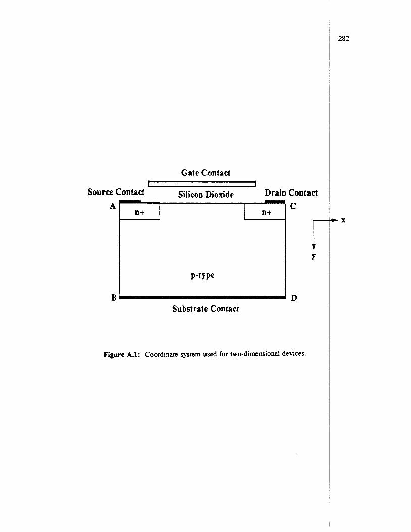
Gate Contact t I
Source Contact Silicon Dioxide Drain Contact
BA
P-tYPe
D
Figure A.l: Coordinate system used for two-dimensional devices.
Y r
282
283
YMESH YMESHNO YPOS
XPOS (YPOS) is the X Cy) position (in p) of the mesh point speci
XMESHNO (YMESHNO). The mesh parameters, XMESH and YMESH, can
any number of times to generate a nonunifom grid.
Example:
XMESH 1 0 XMESH 11 1 XMESH 51 2 YMESH 1 0 YMESH 21 2
The above command line specifies the two-dimensional mesh as follows. The1 simu-
lation region is divided into subdomains by a 51 x 21 mesh. The mesh spacing is npnuni-
form in the X direction and uniform in the Y direction. 1
A.6.2. Doping Description
The doping profile for the device is specified by analytical formulas. The ajlowed
two-dimensional doping profile types are uniform and Gaussian. The general fqrm of
each of these profiles is as follows
A.6.2.1. Two-Dimensional Uniform Doping Profile
General form:
UNIF CONC XLO XHI YLO YHI
UNIF specifies a uniform doping in the rectangle formed by XLO, XHI and
YHI. XLO, XHI and YLO, YHI are given in cm. CONC is the doping level in cr
YLO,
I - ~ . A
negative value is specified for a p-type material and a positive value for an h-type
material. The doping N ( x ) is calculated using the following expression,
XLO 5 x S XHI and YL.0 5 y I YHI otherwise
284
Examples:
UNIF 1E16 0 1 E 4 0 0.2E-4
This defines a n-type uniform doping of 1 x 10l6 for the rectangular bgion
O S X S l p m a n d O S Y S 0 . 2 p n t . I
UNIF -2.5E16 0 4E-4 1E-4 2E-4
This defines a p-type uniform doping of 2.5 x 10l6 for the rectangular I
O I X < 4 p n and lpm IY $ 2 ~ .
A.622. Two-Dimensional Gaussian Implantation Doping Profile
General form:
GIMP CONC CHAR POS LATRATIO DIRECTION XLO XHI YLO YHI
GIMP specifies a Gaussian implantation profile with a peak concentration C
in ~ m - ~ , a characteristic length of CHAR in cm, and the peak is located at POS ii
CONC is a negative value for a p-type material. DIRECTION is the axis along
the profile is directed; 0 for the X axis and 1 for the Y axis. The lateral pro:
assumed to have the same form but the characteristic length is shrunk by a fac
LATRATIO. The rectangle specified by XLO, XHI and YLO, YHI bounds the pro
a region inside the device. Within this rectangle the profile is a Gaussian profile
the principal axis. Outside the rectangle the profile falls off along the lateral axis ac
ing to LATRATIO.
Examples:
GIMP 1E19 1.6E-4 20E-4 0.8 1 0 1E-4 0 0
This defines a n-type Gaussian profile of peak concentration 1 x 10¹⁹ cn
characteristic length of 1.6p1, with the peak of the profile placed at 20p1. The I
mgion
INC
em.
hich
le is
)r of
le to
,long
nrd-
, a
.ofile
-3
is aligned to the Y axis and the lateral profile has a characteristic length of 0.8 til
primary profile. The doping is assumed to be Gaussian in the Y direction in the
0 5 X 5 lpm . Outside this region the profile falls of along the X axis as a G
profile with a chatacteristic length of 0.8 x 1 . 6 ~ = 1 . 2 8 ~ . GIMP -1E15 1.2E-4 0 0.1 0 0 0 0 3E-4
This defines a p-type Gaussian profile of peak concentration 1 x 10''
teristic length of 1 . 2 ~ , with the peak of the profile at Ow. The profile is alii
the X axis and the lateral profile has a characteristic length of 0.1 times the 1
profile. The doping is assumed to be Gaussian in the X direction in the
0 I Y I 0 . 5 ~ . Outside this region the profile falls of along the Y axis as a G
profile with a characteristic length of 0.1 x 1 . 2 ~ = 0 . 1 2 ~ .
A.63. Region Description
285
6 the
rgion
ssian
arac-
:d to
mary
:gion
ssian
The REGION parameter describes the presence of different materials in the
specified mesh. A region is specified as follows,
General form: I
REGION XMESHLO XMESHHI Yh4ESHLO YMESHHI
REGION is either SILICON or OXIDE. XMESHLO, XMESHHI, YMESHL@, and
YMESHHI are mesh numbers that define a rectangle whose material type is specifled by
REGION.
Example:
OXIDE 1 21 1 5 SILICON 1 21 5 11
The above command line demarcates a silicon and an oxide region on i
dimensional mesh. The rectangle formed by XMESH numbers 1 and 21 and Y1
two-
E S H
286
TH numbers 1 and 5 is made up of oxide, whereas the rectangle formed by
numbers 1 and 21 and YMESH numbers 5 and 1 1 constitutes the silicon region. I
I
A.6.4. Contact Description
The CONTACT parameter specifies the location of contact nodes on the rec
lar mesh. A specific sequence has to be used for each device. For the numerical
the CONTACT model parameter is given in the sequence positive node, and m
node. For the numerical bipolar transistor CONTACT’S are specified as collector
and emitter nodes. In the case of the numerical MOSFET the CONTACT seque
drain, gate, sourcx, and substrate nodes. The contact nodes to silicon are assumec
ohmic, whereas the contact to an oxide region is assumed to be an aluminum/
contact.
General form:
CONTACT XMESHLO XMESHHI YMESHLO YMESHHI
XMESHLO, XMESHHI, YMESHLO, and YMESHHI define the mesh nL
for the CONTACTS. These are the terminals at which the device is attached to the
nal circuit.
Example: Contacts for a MOSFET
CONTACT 28 31 5 5 CONTACT 5 27 1 1 CONTACT 1 4 5 5 CONTAC
19 19
The contacts are specified in the sequence drain, gate, source, and bulk (sub;
It is seen that contacts can be either horizontal or vertical consistent with the recu
grid used for space discretization.
angu-
diode
;ative
base,
ice is
to be
- P l y
nbers
:xter-
1 3 1
rate).
gular
287
A.6.S. Level Parameter
The LEVEL model parameter is used to specify the dimensionality of the I
Specifying LE-1 implies a onedimensional device and LEVEL2 specifies ;
dimensional device. The default value is 1 for numerical diodes and BIT models.
the MOSFET is a two-dimensional device, it does not require a LEVEL specifil
and LEVEL is an invalid parameter.
A.6.6. One-Carrier Simulations
For MOSFETs, simulation of one carrier-continuity equation provides good
lodel.
two-
Since
ation,
accu-
racy for most of the operating range. However, for conditions like avalanche genekation
and punchthru both carrier-continuity equations have to be solved. A flag can be u$ed to
specify the use of one-carrier simulation when it is known a priori that the MOFFET
will be operating under normal conditions. The model parameter is denoted ONEt. By
default both carriercontinuity equations are solved, and ONEC specifies that onlj one-
carrier simulation should be performed. This model parameter is applicable ody to
numerical MOSFET models and is an invalid parameter for the other numerical devices.
A.7. Example Circuits
A.7.1. Circuit 1
The following deck determines the dc operating point of a simple RTL invert&r cir-
cuit. The bipolar transistor is assumed to be a one-dimensional device with a udiform
doping profile as shown in Figure A.2. A uniform grid is used for the simulations.
RTL INVERTER CIRCUIT VIN 1 0 DC 4
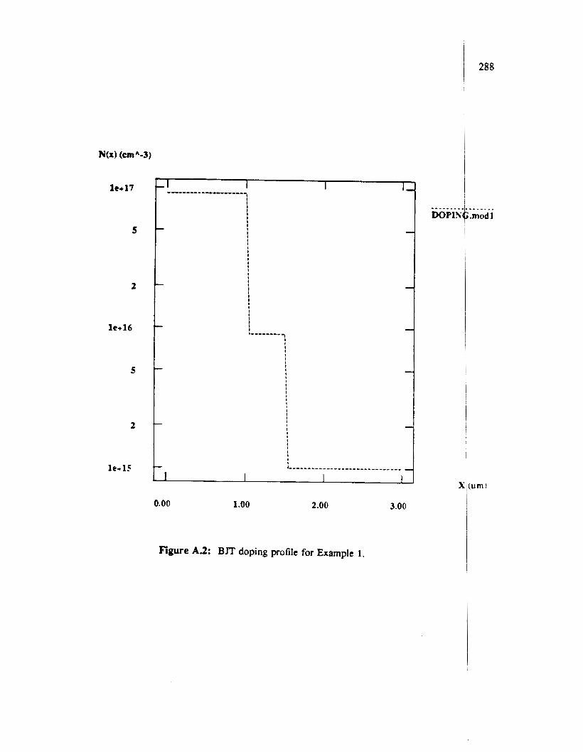
lc+17
s
2
le+16
5
2
l e + l S
0.00 1.00 2.00 3.00
Figure A.2: BJT doping profile for Example 1.
28 8
VCC 12 0 DC 5.0 RCl 12 3 2.5K RBI 1 2 8 K
B 1 3 2 0 MODl AREA = 1U
.MODEL MODl NBJT + NBGN = 1E17 BGNW SRH CONCTAU CONCMOB FIELDMOB AUGER + MESH 1 0 MESH 61 3 + UNIF 1E17 0 1E-4 + UNIF -1E16 0 1.5E-4 + UNIF 1E15 0 5E-4 + SILICON 1 61
.OP
.END
289
I
I
A.7.2. Circuit 2
The following deck computes the transient response of the pull-up circuit of BiC-
MOS driver. A realistic doping profile is used for the transistor as shown in Figure A.3.
This is a typical example of mixed-level simulation with CODECS; the MOSFkT is
modeled by the Level-2 MOS model, whereas a numerical one-dimensional mddel is
used for the bipolar transistor. Note the use of the .OFTION BYPASS = 1. This
specification should be used with numerical models as it provides some speedup.
BiCMOS BUFFER V D D 1 0 0 5 VIN 2 0 0 vc 10 1 0 V B 3 5 0 B1 1 5 4 MOD2 AREA = 0.2U M1 3 2 10 10 MODP W = 60U L = 2U AD = 90P AS = 90P PD = 61U PS 5 6
CL 4 0 lOPF
* Level-2 MOS model
U
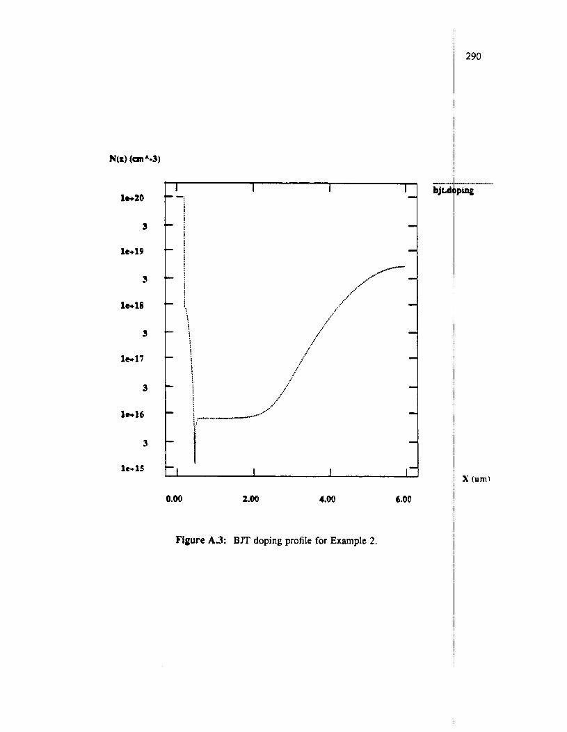
1-20
3
1-19
3
let18
3
1 ~ 1 7
3
1-16
3
1-U
1 1 1 I 1
I I 1
0.00 2.00 4.00 6.00
Figure A 3 : BJT doping profile for Example 2.
290
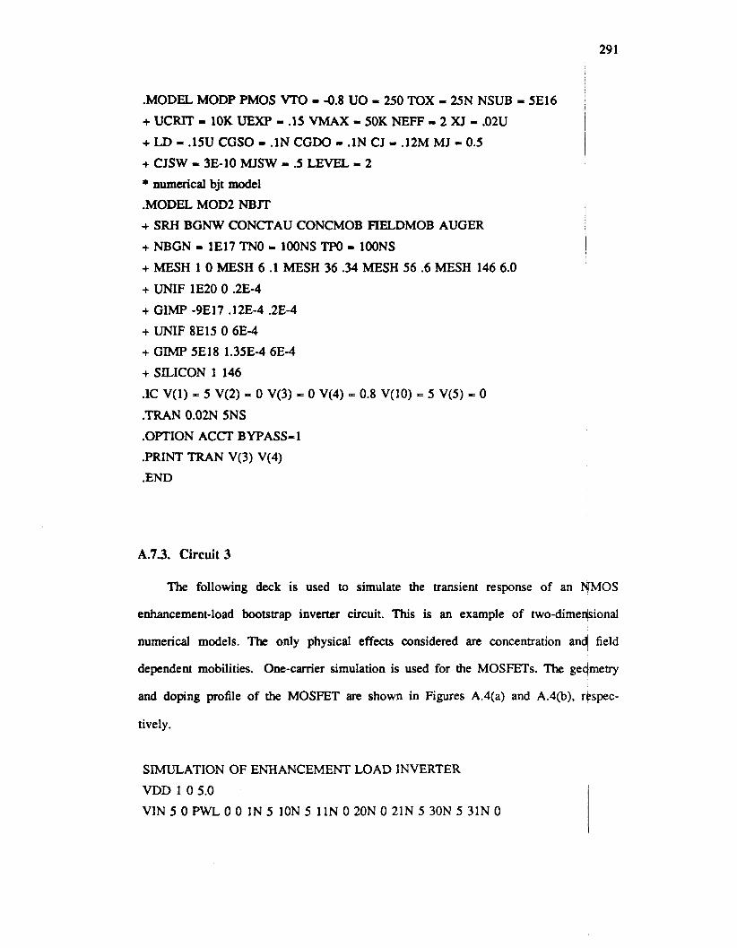
29 1
.MODEL MODP PMOS VTO = -0.8 UO = 250 TOX = 25N NSUB = 5E16 + UCRIT- 10K UEXP = .15 VMAX = 50KNEFF = 2XJ = .02U
+ LD = .15U CGSO = . lN CGDO = . lN CJ = .12M MJ = 0.5 + CJSW = 3E-10 MJSW = 5 LEVEL 2 * numerical bjt model .MODEL MOD2 NBJT + SRH BGNW CONCTAU CONCMOB FIELDMOB AUGER
+ NBGN = 1E17 "NO = lOONS TPO = lOONS
+ MESH 1 0 MESH 6.1 MESH 36.34 MESH 56.6 MESH 146 6.0
+ UNIF 1E20 0 .2E-4 + GIMY -9E17 .12E-4 .2E-4 + UNIF 8E15 0 6E-4 + GIMP 5E18 1.35E-4 6E-4
+ SILICON 1 146
.IC V(1) = 5 V(2) = 0 V(3) = 0 V(4) = 0.8 V(10) = 5 V(5) = 0
.TRAN 0.02N 5NS
.OFTION ACCT BYPASS-I
.PRINT "RAN V(3) V(4)
.END
A.73. Circuit 3
The following deck is used to simulate the transient response of an HMOs
enhancement-load bootstrap inverter circuit. This is an example of two-dime+ional
numerical models. The only physical effects considered are concentration an4 field
dependent mobilities. One-carrier simulation is used for the MOSFETs. The gedmetry
and doping profile of the MOSFET are shown in Figures A.4(a) and A.4(b), respec-
tively.
SIMULATION OF ENHANCEMENT LOAD INVERTER VDD 1 0 5.0 VIN 5 0 PWL 0 0 I N 5 ION 5 11N 0 20N 0 21N 5 30N 5 31N 0
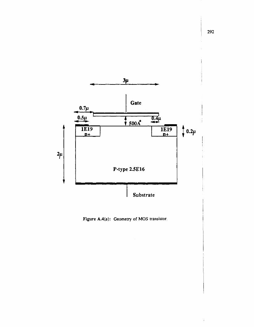
I
Figure A.4(a): Geometry of MOS transistor.
1E19 1E19 n+ n+
P-type 25E16
1
292
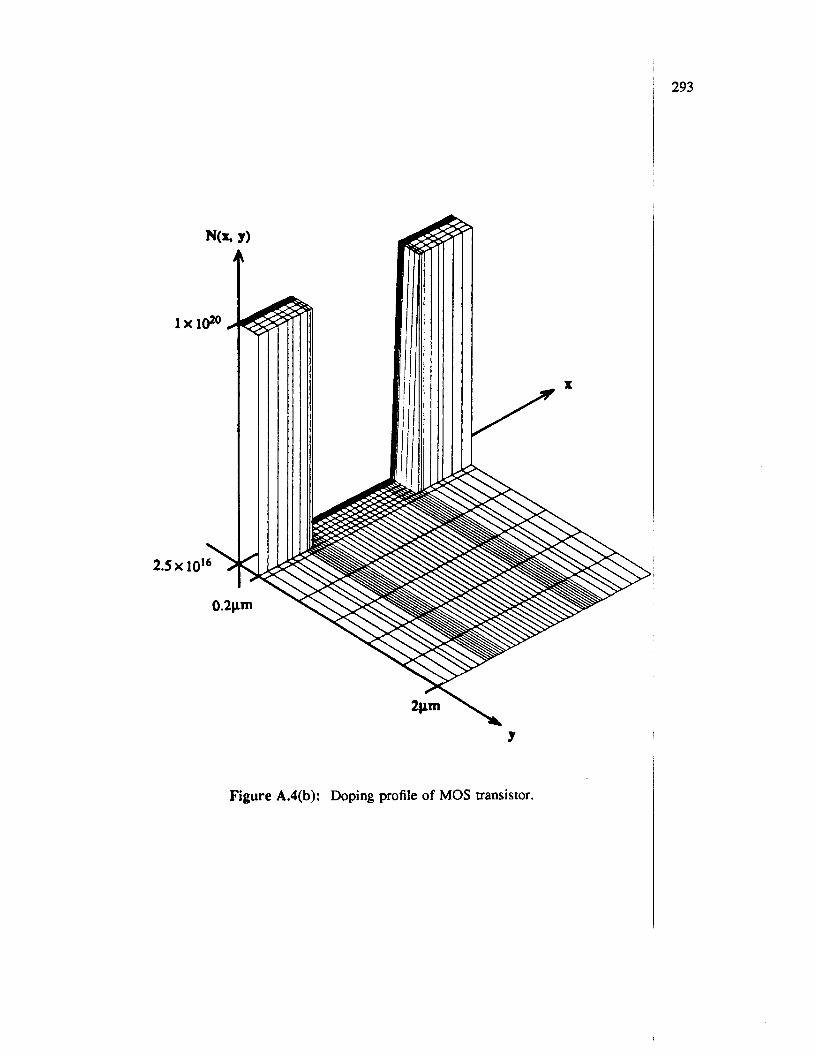
l X l P . #
Y
Figure A.4(b): Doping profile of MOS transistor.

N1 1 1 3 O M O D l W " H = 5 E - 4 N2 1 3 4 4 MODl WIDTH = 5e-4 N3 4 5 0 0 MODl WIDTH = 5E-4
CL 4 0 .lPF
.MODEL MODl N M O S + CONCMOB FIELDMOB ONEC + XMESH 1 0 XMESH 4 0.6 XMESH 5 0.7 + XMESH 7 1.0 XMESH 11 1.2 XMESH 21 3.2 + XMESH 25 3.4 XMESH 27 3.7 XMESH 28 3.8 XMESH 31 4.4
+ YMESH 1 -.05 YMESH 5 0.0 YMESH 9 0.05 YMESH 14 .3 YMESH 19 2.0 + UNIF 1E20 0 l.lE-4 0 .2E-4
+ UNIF 1E20 3.3E-4 4.4E-4 0 .2E-4 + UNIF -2.5E16 0 4.4E-4 0 2E-4 + UNIF -1E16 0 4.4E-4 0 .05E-4
+ OXIDE 5 27 1 5
+ SILICON 1 3 1 5 19 + CONTACT 28 31 5 5
+ CONTACT 5 27 1 1
+ CONTACT 1 4 5 5
+ CONTACT 1 3 1 19 19 .TRAN .2NS 40NS
.OPTIONS ACCT BYPASS=l
.PRINT TRAN V(3) V(4)
.END
A.7.4. Circuit 4
The following deck is used to simulate the turnoff transient of a two-dime
diode with an inductive load and a RC snubber circuit. Notice the use of the I
parameter. The doping profile is shown in Figure AS.
TWO-DIMENSIONAL PIN DIODE CIRCUIT VIN 1 0 PWL 0 0.8 In -50
294
sional
EVEL
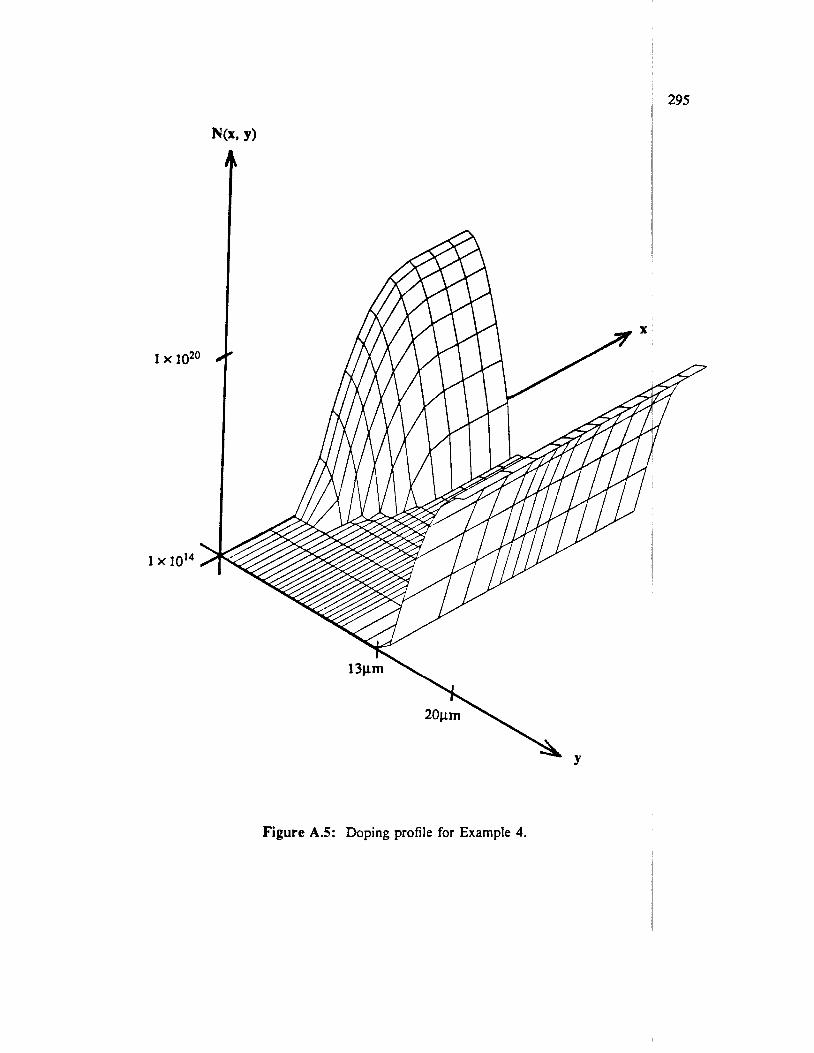
295
Figure AS: Doping profile for Example 4.

L1 1 2 0.5UH V D 2 3 D C O A1 3 0 MODl WIDTH = 0.2 V R C 2 4 D C O R 1 4 5 100
C1 5 0 1NF
.MODEL MODl NUMD LEVEL = 2 + TNO = 20N Tpo = 20N SRH CONCTA J CONCMOB FIELDMOB AUGER + XMESH 1 0 XMESH 2.2 XMESH 4 .4 XMESH 8 .6 XMESH 13 1.0
+ YMESH 1 0 YMESH 9 4 YMESH 24 10 YMESH 29 15 YMESH 34 20
' 296
1
+ GIMP -1E20 1.076E-4 0 0.1 1 0.75E-4 1E-4 0 0 + UNIF 1E14 0 1E-4 0 20E-4 + G M P 1E20 1.614E-4 20E-4 0.8 1 0 1E-4 0 0 +CONTACT8 13 1 1 + CONTACT 1 13 34 34
+ SILICON 1 13 1 34
.OPTION ACCT BYPASS-1
.TRAN 1N lOON
.PRINT TRAN V(3) I(VIN)
.END
297
APPENDIX B
CODECS Benchmark Circuits
RTL INVERTER CIRCUIT
VIN 1 0 DC 1 PWL 0 4 1N 0 VCC 12 0 DC 5.0 RC1 12 3 2.5K RBI 1 2 8 K B1 3 2 0 MODl AREA = 1E-6 *NUMERICAL MODEL FOR BIPOLAR TRANSISTOR
.MODEL MODl NBJT BASE 1.25E-4 + NBGN = 1E17 BGNW SRH CONCTAU CONCMOB FIELDMOB AUGER + MESH 1 0 MESH 61 3 + UNIF 1E17 0 1E-4 + UNIF -1E16 0 1.5E-4
+ UNIF 1E15 0 5E-4
+ SILICON 1 61 .OFTION A C n BYPASS-1 .TMN 0.5N 5N *.OP .PRINT TRAN V(3) .END
COLPI'IT'S OSCILLATOR CIRCUIT R 1 1 0 1 B1 2 1 3 MODl AREA = 1E-6 v c c 4 0 5 FtL 4 2 750 c1 2 3 500P C2 4 3 4500P
298
L14 2 5UH RE 3 6 4.65K VEE 6 0 DC -15 PWL 0 -15 1N -10
.MODEL MODl NBJT BASE 1.25E-4
+ NBGN = 1 ~ 1 7 BGNW SRH AUGER cor + MESH 1 0 MESH 61 3 + SILICON 1 61 + UNIF 1E17 0 1E-4 + UNIF -1E16 0 1.5E-4 +UNlF 1E1505E-4 .OPTION A C n BYPASS=l ."RAN 30N 12U *.OP .PRINT TRAN V(2) .END
CTAI cor :MOB FIELDh
VOLTAGE CONTROLLED OSCILLATOR
RCI 7 5 1K
RC2 7 6 1K
B5 7 7 5 MOD1 AREA 1E-6 B6 7 7 6 MOD1 AREA = 1E-6 B3 7 5 2 MODI AREA 1E-6 B4 7 6 1 MOD1 AREA = 1E-6
IB1 2 0.5MA IB2 1 0 SMA
CBI 2 0 1PF CB2 1 0 1Pf
B1 5 1 3 MODl AREA = 1E-6 B2 6 2 4 MODI AREA = 1E-6 c 1 3 4 .IuF IS1 3 0 DC 2.5MA PULSE 2.5MA 0.5MA 0 IUS IUS 50MS IS2 4 0 1MA
vcc 7 0 10 .MODEL MODI NBJT BASE 1.25E-4
OB
299
+ SRH AUGER BGNW CONc'rAU CONCMOB FIELDMOB NBGN = 1E17
+ MESH 1 0 MESH 61 3
+ SILICON 1 61 + UNIF 1E17 0 1E-4 + UNIF -1E16 0 1.5E-4 +UNIF 1E15OSE-4 .OPI"ION ACCT BYPASS-1 .TRAN 3US 6OOUS 0 3US *.OP
.PRINT "RAN V(4)
.END
FOUR RTL INVERTER CHAIN V I N l O D C O P W L O O l N 5
VCC 12 0 DC 5.0 RC1 12 3 2.5K
RBI 128K B1 3 2 0 MODl AREA = 1E-6
R B 2 3 4 8 K
RC2 12 5 2.5K B2 5 4 0 MODl AREA = 1E-6
RB3 5 6 8K RC3 12 7 2.5K
B3 7 6 0 MODl AREA = 1E-6 RB4 7 8 8K RC4 12 9 2.5K B4 9 8 0 MODl AREA = 1E-6 .MODEL MOD1 NBJT BASE = 1.25E-4 + NBGN = 1E17 BGNW SRH AUGER CONCTAU CONCMOB FIELDMOB + MESH 1 0 MESH 61 3.0 + SILICON 1 61 + UNIF 1E17 0 1E-4
+ UNIF -1E16 0 1.5E-4 + UNIF 1E15 0 5E-4
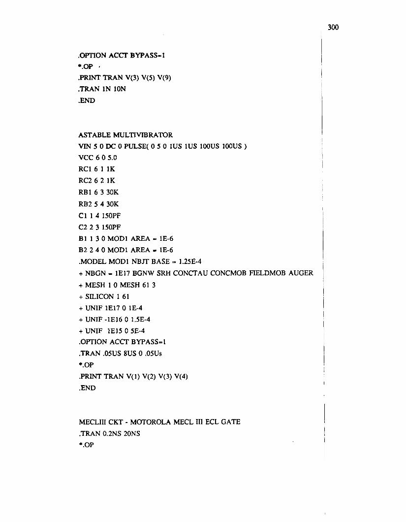
.OPTION ACCT BYPASS-1 *.OP .PRINT "RAN V(3) V(5) V(9) ."RAN 1N 10N .END
ASTABLE MULTIVIBRATOR VIN 5 0 DC 0 PULSE( 0 5 0 IUS IUS lOOUS lOOUS ) VCC 6 0 5.0 RC1 6 1 1K RC2 6 2 1K
RBI 6 3 30K
RB2 5 4 30K C1 1 4 150PF
C2 2 3 l5OPF B1 1 3 0 MOD1 AREA = 1E-6 B2 2 4 0 MODl AREA 1E-6
.MODEL MODl NBJT BASE t 1.25E-4
+ NBGN = 1E17 BGNW SRH CONCTAU CONCMOB FIELDMOB AUGER
+ MESH 1 0 MESH 61 3 + SILICON 1 61
+ UNIF 1E17 0 1E-4 + UNIF -1E16 0 1.5E-4 + UNIF lEl5 0 5E-4 .OPTION ACCr BYPASS-1
.TRAN .05US 8US 0 .05Us *.OP .PRINT TRAN V(l) V(2) V(3) V(4)
.END
MECLIII CKT - MOTOROLA MECL 111 ECL GATE .TRAN 0.2NS 20NS *.OP
300
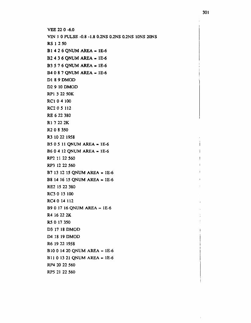
30 1
VEE 22 0 4.0
VIN 1 0 PULSE -0.8 -1.8 0.2NS 0.2NS 0.2NS lONS 20NS RS 1 2 50
B 1 4 2 6 QNUM AREA 1E-6
B2436QNUMAREA-1E-6 B3 5 7 6 QNUM AREA = 1E-6 B4 0 8 7 QNUM AREA = 1E-6 D 1 8 9 DMOD D2 9 10 DMOD Rpl 3 22 50K RC10 4 100
R C 2 0 5 112
RE 6 22 380
R1 7 22 2K
R2 0 8 350
R3 10 22 1958 B5 0 5 11 QNUM AREA = 1E-6 B6 0 4 12 QNUM AREA = 1E-6 RF'2 11 22560
RP3 12 22 560 B7 13 12 15 QNUM AREA 1E-6 B8 14 16 15 QNUM AREA = 1E-6 RE2 15 22 380 RC3 0 13 100 RC4 0 14 112 B9 0 17 16 QNUM AREA = 1E-6
R4 16 22 2K
Rs 0 17 350 D3 17 18 DMOD
D4 18 19 DMOD R6 19 22 1958 BlO 0 14 20 QNUM AREA = 1E-6 B11 0 13 21 QNUM AREA = 1E-6 RP4 20 22 560 RP5 21 22 560
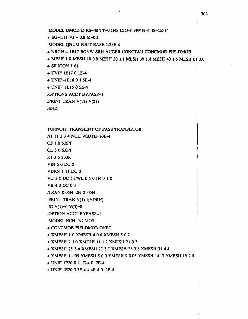
.MODEL DMOD D RS-40 TI'4.1NS CJO-0.9PF N=1 IS-1E-14 + EG-1.11 VJ 0.8 M-0.5
.MODEL QNUM NBJT BASE 1.25E-4
+ NBGN - 1E17 BGNW SFW AUGER CONCTAU CONCMOB FIELDMOB
+ MESH 1 0 MESH 10 0.9 MESH 20 1.1 MESH 30 1.4 MESH 40 1.6 MESH 6 + SILICON 1 61 + UNIF 1E17 0 lE-4 + UNIF -1E16 0 1.5E-4
+UNIF lEl505E-4
.OPTIONS ACCT BYPASS-1
.PRINT TRAN V(12) V(21)
.END
TURNOFF TRANSIENT OF PASS TRANSISTOR N1 11 2 3 4 NCH WIMH=20E-4
CS 1 0 6.OPF CL 3 0 6.OPF R 1 3 6 200K VIN 6 0 DC 0 VDRN 1 1 1 D C O VG 2 0 DC 5 PWLO 5 0.1N 0 1 0 VB 4 0 DC 0.0 .TRAN O.05N .2N 0 .05N .PRINT TRAN V( 1) I(VDRN) .IC V(1)=0 V(3)=0
.OPTION ACCT BYPASS=l
.MODEL NCH NUMOS
+ CONCMOB FIELDMOB ONEC + XMESH 1 0 XMESH 4 0.6 XMESH 5 0.7 + XMESH 7 1.0 XMESH 11 1.2 XMESH 21 3.2 + XMESH 25 3.4 XMESH 27 3.7 XMESH 28 3.8 XMESH 31 4.4 + YMESH 1 -.05 YMESH 5 0.0 YMESH 9 0.05 YMESH 14 .3 YMESH 19 2.0 + UNIF 1E20 0 1.1E-4 0 .2E-4 + UNIF 1E20 3.3E-4 4.4E-4 0 .2E-4
302
3.0
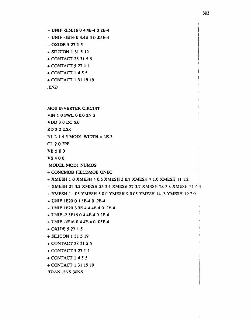
303
+ UNIF -2.5E16 0 4.4E-4 0 2E-4
+ UNIF -1E16 0 4.4E-4 0.05E-4
+ OXIDE 5 27 1 5 + SILICON 1 31 5 19 + CONTACT 28 31 5 5
+ CONTACT 5 27 1 1 + CONTACT 1 4 5 5
+CONTACT 1 3 1 19 19
.END
MOS INVERTER CIRCUIT VIN 1 0 PWL 0 0.0 2N 5
VDD 3 0 DC 5.0
RD 3 2 2.5K
N1 2 1 4 5 MODl WIDTH = 1E-3
CL 2 0 2PF VB500 VS400 .MODEL MODl NUMOS + CONCMOB FIELDMOB ONEC + XMESH 1 0 XMESH 4 0.6 XMESH 5 0.7 XMESH 7 1.0 XMESH 11 1.2
1
I
i
+ XMESH 21 3.2 XMESH 25 3.4 XMESH 27 3.7 XMESH 28 3.8 XMESH 31 4.k
+ YMESH 1 -.OS YMESH 5 0.0 YMESH 9 0.05 YMESH 14 .3 YMESH 19 2.0 + UNIF 1E20 0 l.lE-4 0 .2E-4 + UNIF lE20 3.3E-4 4.4E-4 0 .2E-4 + UNIF -2.5E16 0 4.4E-4 0 2E-4 + UNIF -1E16 0 4.4E-4 0 .05E-4 + OXIDE 5 27 1 5
+ SILICON 1 31 5 19
+CONTACT 28 31 5 5
+ CONTACT 5 27 1 1
+ CONTACT 1 4 5 5 + CONTACT 1 31 19 19
I
1
I
. T U N .2NS 30NS

304
.IC V(1) = 0.0 V(2) - 5.0 V(3)d.O V(4)a.O V(5)=0.0
.OFTIONS ACCT BYPASS-1
.PRINT "RAN V(1) V(2)
.END
CHARGE PUMP CIRCUIT VIN 4 0 PULSE 0 5 15NS 5NS 5NS SONS IOONS VDD 5 6 PULSE 0 5 2SNS 5NS 5NS 50NS lOONS VBB 0 7 PULSE 0 5 0 5NS 5NS 50NS lOONS RD 6 2 10K N1 5 4 3 7 MODI WIDTH = 1E-2 V S 3 2 0
v c 2 1 0 C2 1 0 lOPF
.MODEL MODI NUMOS + CONCMOB FIELDMOB ONEC + XMESH 1 0 XMESH 3 0.4 XMESH 7 0.6 XMESH 15 1.4 + XMESH 19 1.6 XMESH 21 2.0
+ YMESH 1 0 YMESH 4 0.015 YMESH 8 0.05 YMESH 12 0.25
+ YMESH 14 0.35 YMESH 17 0.5 YMESH 21 1.0 + UNIF 1E18 0 0.5E-4 0.015E-4 .25E-4
+ UNIF 1E18 1.5E-4 2.OE-4 0.015E-4 0.25E-4 + UNIF -1E15 0 2E-4 0.015E-4 1E-4 + UNIF -1.3E17 0.5E-4 1.5E-4 0.015E-4 .05E-4 +OXIDE 5 17 1 4
+ SILICON 1 21 4 21 + CONTACT 18 21 4 4
+ CONTACTS 17 1 1
+ CONTACT 1 4 4 4 + CONTACT 1 21 21 21 .IC V(4) = 0 V(3) = 1.0 V(2) = 1.0 V(l) = 1.0 V(5)=1.0 V(7)xO.O V(6)=1.0 *.OP .TRAN 2NS 200NS
.OPTIONS ACCT BYPASS-1

.PRINT TRAN V(1) V(2)
.END
APPENDIX C
Source Listing of CODECS
The source listing of CODECS is available at the following address:
Software Distribution Office
Industrial Liaison Program
Department of Electrical Engineering and Computer Sciences
University of California
Berkeley, CA 94720
306
!
i
307
I
J. G. Rollins and J. Choma, "Mixed-Mode PISCES-SPICE Coupled C
and Device Solver," IEEE Trans. Computer-Aided Design, vol. 7, pp.
REFERENCES
rcuit
862-
Chapter 1
867, Aug. 1988.
C. H. Price, "Two-Dimensional Numerical Simulation of Semiconductc
ices," Ph. D. Dissertation, Stanford University, Stanford, 1982.
E1.91 . Dev-
rcuits,
[ adeh,
Chapter 2
A. L. Sangiovanni-Vincentelli, "Circuit Simulation", in Computer Design
for VLSI Circuits, P. Antognetti, D. 0. Pederson, and H. De Man
Groningen, The Netherlands: Sijthoff and Noordhoff, pp. 19-1 13, 1981.
L. 0. Chua and P. M. Lin Computer-Aided Analysis of Electronic
Algorithms and Computational Techniques, Prentice Hall Inc., New
1975.
12.11
P.21
12.31
12.41
12.51
12.61
12.71
Aids
(Ed.tors),
Cirtcuirs:
Jmey ,
L. 0. Chua, C. A. Desoer, E. S. Kuh, Lineur d Nonlinear C
McGraw-Hill Book Company, NY 1987.
W. T. Weeks, A. J. Jimenez, G. W. Mahoney, D. Mehta, H. Qasserr
308
and T. R. Scott, "Algorithms for ASTAP - A Network Analysis Proqam,"
IEEE Trans. Circuit Theory, vol. CT-20, pp. 628-634, Nov. 1973.
L. W. Nagel, "SPICE2: A Computer Program to Simulate Semiconduct r Cir-
cuits", Memo. No. ERL-M520, Electronics Research Laboratory, Unive ity of
California, Berkeley, May 1975. i C. W. Ho., A. E. Ruehli, and P. A. Bremn, "The Modified Nodal Ap roach
to Network Analysis", IEEE Trans. Circuits and Systems , vol. CAS-2b, pp.
504-509, June 1975.
4 ~
T. Quarles, A. R. Newton, D. 0. Pederson, and A. Sangiovanni-Vincelntelli,
SPICE 3BZ User's Guide, Dept. of Electrical Engineering and Cornput+ Sci-
ences, University of California, Berkeley, April 1988. ~
309
W. J. McCalla, Computer-Aided Circuit Simulation Techniques, Kluwe Pub-
lishers, 1987.
R. K. Brayton, E G. Gustavson, and G. D. Hachtel, "A New Efficient iAlgo-
nthm for Solving Differential- Algebraic Systems Using Implicit Bacbard
, 12.81
I P.91
Differentiation Formulas," IEEE Proc., vol. 60, pp. 98-108, Jan. 1972.
[2.10] R. Saleh, "Nonlinear Relaxation Algorithms for Circuit Simulation," Memo
No. UCBIERL M87121, Electronics Research Laboratory, University of Cali-
fornia, Berkeley, April 1987.
[2.11] E. Lelarasmee, "The Waveform Relaxation Method for Time Dqmain
Analysis of Large Scale Integrated Circuits: Theory and Applications," kemo
No. UCBIERL M82140, Electronics Research Laboratory, University of Cali-
fornia, Berkeley, May 1982.
[2.12] J. White, "The Multirate Integration Properties of Waveform Relaxation) with
Application to Circuit Simulation and Parallel Computation," Mer@ No.
UCBIERL 85/90, Electronics Research Laboratory, University of Cali$rnia,
Berkeley, Nov. 1985.
[2.13] G. Marong and A. Sangiovanni-Vincentelli, "Waveform Relaxatiod and
Dynamic Partitioning for Transient Simulation of Large Scale Bipolat Cir-
cuits," Proc. IEEE ICCAD-85, Santa Clara, CA, pp. 32-34, Nov. 1985.
J. Vlach and K. Singhal, Computer Methocis for Circuit Analysis and Dksign,
Van Nostrand Reinhold Company, 1983.
[2.14]
[2.15] I. Getreu, Modeling The Bipolar Transistor, Tekoonix, 1976. 1
[2.16] H. Shichman and D. A. Hodges, "Modeling and Simulation of
Field-Effect Transistor Switching Circuits", I€€€ J.
SC-3, pp. 285-289, Sept. 1968.
310
(2.171
[2.18]
[2.19]
P.201
[2.21]
[2.22]
[2.23]
[2.24]
[2.251
H. K. Gummel and H. C. Poon, "An Integral Charge Control Model o Bipo-
L. J. Turgeon and J. R. Mathews, "A Bipolar Transistor Model of asi-
Saturation for use in Computer-Aided Design (CAD)," IEDM Digest 1. Tech.
lar Transistors," Bell Sysr. Tech. J., pp. 827-852, May 1970.
Papers, Washington D.C. Dec. 1980.
Dirks, "A Unified Circuit Model for Bipolar Transistors Including uasi-
Saturation Effects," IEEE Tram. Electron Devices, vol. ED-32, pp. 1103-
G. Merckel, "CAD Models of MOSFETS," in Process and Device M eling
for Inregrated Circuir Design, F. Van de Wiele, W. L. Engl, and i' P. G.
G. M. Kull, L. W. Nagel, S. W. Lee, P. Uoyd, E. J. Frendergast,
1113, June 1985.
Jespers (Editors), Noordhoff, Leyden, The Netherlands, 1977.
L. M. Dang, "A Simple Current Model for Short-Channel IGFET nd its
Application to Circuit Simulation," IEEE J. Solid-State Circuits, vol. C-14,
I
4 pp. 383-391, April 1979.
H. I. Hanafi, L. H. Camnitz, and A. J. Dally, "An Accurate and imple 3 MOSFET Model for Computer-Aided Design," IEEE J. Solid-State Ci
vol. SC-17, no. 5, pp. 882-891, Oct. 1982.
A. Vladimirescu and S. Liu, "The Simulation of MOS Integrated C
using SPICE2," Memo No. UCBIERL M8017, Electronics Research L
tory, University of California, Berkeley, Feb. 1980.
S. Liu and L. W. Nagel, "Small-Signal MOSFET Models for Analog (
Design," IEEE J. Solid-State Circuits, vol. SC-17, pp. 993-998, Dec. 19
G. T. Wright, "Simple and Continuous MOSFET Models for Computer-
Design of VLSI," IEE Proc., vol. 132 part I, pp. 187-194, Aug. 1985.
cuits
)ora-
rcuit
!.
.ided
31 1
3 and i2.261 Y. A. Elmansy and A. R. Boothroyd, "A New Approach to the The0
Modeling of Insulated-Gate Field-Effect Transistors," IEEE Trans. El&ron
Devices, vol. ED-24, pp. 241-253, March 1977.
G. Baccarani, M. Rudan, and G. Spadini, "Analytical i.g.f.e.t Model lnclbding
Drift and Diffusion Currents," IEE J. Solid-State and Electron Deviced, vol.
[2.27]
2, pp. 62-68, March 1978.
[2.28] I. R. Brews, "A Charge Sheet Model for the MOSFET," Solid-State Elemon-
ics, vol. 21, pp. 345-355, 1978.
[2.29] C. Turchetti and G. Masetti, "A CAD-Oriented Analytical MOSFEX Model
for High-Accuracy Applications,'' IEEE Trans. Computer-Aided Design; vol.
CAD-3, pp. 117-122, July 1984.
12.301 M. H. White, F Van de Wiele, and J. P. Lambot, "High-Accuracy MOS
Models for Computer-Aided Design," IEEE Trans. Electron Devices, vol.
ED-27, pp. 899-906, May 1980. 1
[2.31] P. Yang, B. D. Epler, P. K. Chatterjee, "An Investigation of Charge Cunser-
vation Problem for MOSFET Circuit Simulation," IEEE J. Solid-Srate Cir-
cuits, vol. SC-18, pp. 128-138, Feb. 1983.
B. J. Sheu, "MOS Transistor Modeling and Characterization for Circuit airnu-
lation," Memo No . UCBIERL M8518.5, Electronics Research Labor#ory,
1
[2.32]
1 University of California, Berkeley, Oct. 1985. i
[2.33] M. Bagheri and Y. Tsividis, "A Small-Signal Dc-to-High Frequency bon-
quasistatic Model for the Four-Terminal MOSFET Valid in All Regia@ of
Operation," IEEE Trans. Electron Devices, vol. ED-32, pp. 2383-239 1, pov.
1985.
I
C. Turchetti, P. Mancini, G. Masetti, "A CAD-Oriented Non-Quasi-Static (2.341
C. G. Mini, P. K. KO, and J. L. Moll, "The Effect of High Fields on
[2.35]
[2.36]
[2.37]
MOS
[2.38]
t2.393
t2.401
[2.41]
E. Khalily, P. H. Decher, D. A. Teegarden, "TECAP2: An Interactive 9 c e
Characterization and Model Development System," Proc. I€E€ KC&-84,
Santa Clara, CA, pp. 149-151, Nov. 1984.
K. Doganis and D. L. Scharfetter, "General Optimization and Extractionlof IC
Device Models," IEEE Trans. Electron Devices, vol. ED-30, pp. 121941228,
Sept. 1983. I
J. L. D'Arcy and R. C. Rennick, "MOSFET Parameter Optimizati for
Accurate Output Conductance Modeling," Proc. I985 IE€€ CICC , Po and,
OR, pp. 512-513, May 1985. 1 I
~ 27, pp. 1359-1367, Aug. 1980. ~
[2.42]
ne1 Length and Series Resistance of LDD MOSFET's," IEEE ,Trans. El
G. J. Hu, C. Chang, and Y. Chia, "Gate-Voltage-Dependent Effective
313
Devices, vol. ED-34, pp. 2469-2475, Dec. 1987. I 12.431
(2.441
[2.47]
[2.48]
r2.491
[2.50]
[2.51]
G. Huang and C. Wu, "An Analytic I-V Model for Lightly Doped /Drain
(LDD) MOSFET devices," IEEE Tram. Electron Devices, vol. ED-34, pp.
D. E. Ward and R. W. Dunon, "A Charge-Oriented Model for MOS T
tor Capacitances," IEEE J. Solid State Circuits, vol. SC-13, pp. 703-70
S. E. Laux, "Techniques for Small-Signal Analysis of Semiconductor Dev-
ices," IEEE Tram. Electron Devices, vol. ED-32, pp. 2028-2037, Oct. 1 j 85.
1978.
B. R. Chawla and H. K. Gummel, Transition Region Capacitanb of
Diffused p-n Junctions," IEEE Tram. Electron Devices, vol. ED-18, PPI 178-
195, March 1971.
1311-1322, JUIE 1987.
is-
Oct.
I
S. W. Lee and E. J. Rendergast, "Analytical Relations for Determinirig the
Base Transit Times and Forward-Biased Junction Capacitances of Bepolar
Transistors," Solid-Stute Electronics, vol. 28, pp. 767-773, 1985. i
R. S. Muller and T. I. Kamins, Device Electronics for Integrated Cidcuits,
John Wiley and Sons, New York, 1986.
S. M. Sze, "physics of Semiconductor Devices," John Wiley, 198 1. I
S. K. Ghandhi, Power Semiconductor Devices, John Wiley and Sons, 19p7.
T. Shima, T. Sugawara, S. Moriyama, and H. Yamada, "Three-Dimen@onal
Table Look-Up MOSFET Model for Precise Circuit Simulation," &E J .
Solid-State Circuits, vol. SC-17, pp. 449-454, June 1982.
J. L. Burns, "Empirical MOSFET Models for Circuit Simulation," Me& No. 1
[2.52]
UCBIERL M84143, Electronics Research Laboratory, University of Calif rnia
Berkeley, May 1984. P !
314
[2.53]
[2.54]
[2.55]
[2.56]
[2.57]
[2.58]
[2.59]
[ 2 . W
[2.61]
I
J. Barby, J. Vlach, and K. Singhal, "Optimized Polynomial Splines fol FET
Models," Proc. IEEE ISCAS, Montreal, Canada, pp. 1159-1162, May 19/84.
T. Shim, H. Yamada and R. Dang, "Table Look-up MOSFET Mc$eling
System Using a 2-Dimensional Device Simulator and Monotonic
Cubic Interpolation," IEEE Trans. Computer-Aided Design, vol.
R. S. Gyurcsik, "An Attached Processor for MOS-Transistor
tion,," Memo No. UCBIERL. M86182, Electronics Research
sity of California, Berkeley, Oct. 1986.
E. M. Sentovich, "B-spline Device Models in
T. Shima, "Device and Circuit Simulator
and Device Modeling, W . L. Engl
University of California, Berkeley, 1988.
(North-Holland) pp. 433-459, 1986.
121-126, April 1983.
T. Shima, "Table Lookup MOSFET Capacitance Model for Short 4annel
Devices," IEEE Trans. Computer-Aided Design, vol. CAD-5, pp. 624-632,
Oct. 1986. I
H. K. Dirks and K. Eickhoff, "Numerical Models and Table Models forlMOS
Circuit Analysis," Proc. NASECODE N, Dublin, Ireland, pp. 13-24,l June
A. F. Lachner, "Two-Dimensional Integral Analysis of Bipolar Ju ction
Transistors," Ph. D. dissertation, University of California, Berkeley, 198 .
D. J. Roulston, S. G. Chamberlain, and J. Sehgal, "Simplified Corn uter-
Aided Analysis of Double-Diffused Transistor Including Two-Dime ional
High-Level Effects," IEEE Trans. Elecnon Devices, vol. ED-19, pp. 80 -820,
1985. I
315
Steady State Transistor Calculations,"lEEE Trans. Electron Devices,
ED-1 1, pp. 445-465, at. 1964.
[2.62]
[2.63]
[2.641
[2.65]
vol.
June 1972. !
V. Marash and R. W. Dutton, "Methodology for Submicron Device *ode1
Development," IEEE Trans. Computer-Aided Design, vol. 7 , pp. 29d-306,
Feb. 1988.
M. J. Saccamango, "Efficient Modeling of Small-Geometry MOS 's,"
Research Report No. CMUCAD-87-11, Camegie-Mellon University, itts-
H. J. DeMan and R. Mertens, "SITCAP - A Simulator of Bipolar Trans stors
for Computer-Aided Circuit Analysis Programs," Proc. ISSCC-73, pp. 104-
W. L. Engl, R. b u r , and H. K. Dirks, "MEDUSA - A Simulator for M ular
burgh, Sep. 1987.
105, Feb. 1973.
Circuits," IEEE Trans. Computer-Aided Design, vol. CAD-1, pp. 85-93, April
1982.
+
;
316
13.41
i3.91
[3.10]
r3.113
[3.12]
[3.13]
D. L. Schatfetter and H. K. Gummel, "Large-Signal Analysis of a Qilicon
Read Diode Oscillator," IEEE Trans. Electron Devices, vol. ED-16, pb. 64-
77, Jan. 1969.
A. DeMari, "An Accurate Numerical Steady-State One-Dimensional
of the P-N Junction," Solid-state Electronics, vol. 11, pp. 33-58, Jan. 1$8.
A. DeMari, "An Accurate Numerical One-Dimensional Solution of thb P-N
Junction Under Arbitrary Transient Conditions," Solid-state Electronic$, vol.
11, p ~ . 1021-1053, NOV. 1968.
C. H. Price, "Two-Dimensional Numerical Simulation of Semiconductod Dev-
ices," Ph. D. Dissertation, Stanford University, Stanford, 1982.
G. Baccarani, R. Guemeri, P. Ciampolini, and M. Rudan, "HFIELl$S: A
Highly Flexible 2-D Semiconductor-Device Analysis Program," IProc.
NASECODE-N, Dublin, Ireland, pp. 3-12, June 1985.
A. F. Franz, G. A. Franz, and S. Selberherr, "BAMBI - A Design M d e l for
Power MOSFET's,' Proc. IEEE ICCAD-84, pp. 179-181, Nov. 1984. I
1
~
W. L. Engl, H. K. Dirks, and B. Meinerzhagen, "Device Modeling,"
i I
IEEE, V O ~ . 71, pp. 10-33, Jan. 1983.
E. M. Buturla, P. E. Cottrell, B. M. Grossman, and K. A. Salsburg, "iinite-
Element Analysis of Semiconductor Devices: The FIELDAY program,'! IBM i i I J. Res. Develop., vol. 25, pp. 218-231, 1981. ,
T. Toyabe, K. Yamaguchi, S. Asai, and M. S. Mock, "A Numerical +ode1
for Avalanche Breakdown in MOSFET's," IEEE Trans. Electron D
V O ~ . ED-25, pp. 825-832, July 1978.
E. M. Buturla, P. E. Cottrell, B. M. Grossman, K. A. Salsburg,
Lawlor, C. T. McMullen, "Three-Dimensional Finite-Element
i
317
Semiconductor Devices," Proc. ISSCC-80, pp. 76-77, Feb. 1980.
A. Yoshii, H. Kitazawa, M. Tomizawa, S. Horiguchi, and T. Sudd, "A
Three-Dimensional Analysis of Semiconductor Devices," IEEE Trans. @lee
tron Devices, vol. ED-29, pp. 184-189, Feb. 1982.
i r3.141
[3.15] A. Husain and S. G. Chamberlain, "Three-Dimensional Simulation of VLSI
MOSFETs: The Three-Dimensional Simulation Program WATMOS," tEEE
Trans. Electron Devices, vol. ED-29, pp. 631-638, April 1982.
T. Toyabe, H. Masuda, Y. Aoki, H. Shukuri, and T. Hagiwara, '*&ee-
Dimensional Device Simulator CADDETH with Highly Convergent Matrix
Solution Algorithms," IEEE Trans. Electron Devices, vol. ED-32, pp. !2038-
2044, Oct. 1985.
D. M. Caughey and R. E. Thomas, "Carrier Mobilities in Silicon Empirlically
Related to Doping and Field," Proc. IEEE, vol. 52, pp. 2192-2193,iDec.
1967.
[3.16]
[3.17]
I I
[3.18] N. D. Arora, J. R. Hauser, and D. J. Roulston, "Electron and Hole MobClities I
in Silicon as a Function of Concentration and Temperature," IEEE dram.
Electron Devices, vol. ED-29, pp. 292-295, Feb. 1982.
[3.19] K. Yamaguchi, "Field-Dependent Mobility Model for Two-Dimenqional
Numerical Analysis of MOSFET's," IEEE Trans. Electron Devices, v01.i ED-
26, pp. 1068-1074, July 1979.
[3.20] K. Yamaguchi, "A Mobility Model for Carriers in the MOS Inversion Lqyer,"
IEEE Trans. Electron Devices, vol. ED-30, pp. 658-663, June 1983. I
1 [3.21] S. Selberherr. A. Schutz, H. W. Potzl, "MINIMOS - a Two-Dime ional
MOS Transistor Analyzer," IEEE Trans. Electron Devices, vol. ED-2 , pp.
1540-1550, Aug. 1980. 1 i
318
[3.22] M. Eldredge, "Struchmd PISCES," Annual Research Swnmary: Proce s and
Device Modcling, Stanford Electronics Laboratories, Stanford Unidersity ,
Stanford, 1988.
i
r3.231
[3.24]
[3.251
t3.261
[3.27]
r3.281
[3.30]
J. T. Watt and J. D. Hummer, "Universal Mobility-Field C w e s for El cuons
and Holes in MOS Inversion Layers," Digest of Tech. papers 1987 ymp.
VUI Technology, pp. 82-83, May 1987. 1 I i
R. S. Muller and T. I. Kamins, Device Electronics for Integrated Circuits,
John Wiley and Sons, New York, 1986. I
D. J. Roulston, N. D. Arora, and S. G. Chamberlain, "Modeling and keas-
urement of Minority-Canier Lifetime versus Doping in Diffused Laykrs of
n+-p Silicon Diode,'' IEEE Trans. Electron Devices, vol. ED-29, pp. 28 -291,
Feb. 1982.
I
f A. G. Chynoweth, "Ionization Rates for Electrons and Holes in Silicon,' Phy-
sical Review, vol. 109, pp. 1537-1540, 1958.
A. Schutz, S. Selberherr, and H. W. Pot& "Analysis of Bre down
Phenomena in MOSFET's," IEEE Trans. Computer-Aided Design1 vol.
t
t I
I I
CAD-I, pp. 77-85, April 1982. I
J. W. Slotboom and H. C. De Graaff, "Measurements of Bandgap Narrlwing
in Si Bipolar Transistors," Solid State Electronics, vol. 19, pp. 857-86 Oct.
1976.
R. J. Van Overstraeten, H. J. DeMan, and R. J. Mertens, "Transport
4
tions in Heavy Doped Silicon," IEEE Trans. Electron Devices, vol. "- pp. 290-298, March 1973.
L. Lapidus, G. F. Pinder, Numerical Solution of Partial Differential Eq
in Science and Engineering, John Wiley, New York, 1982.
tions I
319
j3.311 C. S. RafTerty, M. R. Pinto, and R. W. Dumn, "Iterative Methods i Sem-
iconductor Device Simulation," IEEE Trans. Computer-Aided Desigd, vol. .i
CAD-4, pp. 462-471, a t . 1985.
(3.321 G. D. Hachtel, M. H. Mack, R. R. O'Brien, and B. Speelpennig, "Sehcon-
ductor Analysis Using Finite Elements - Part I: Computational Aspects, IBM f J. Res. cmd Dcv., vol. 25, pp. 232-245, 1981. I
[3.33] J. W. Slotboom, "Computer-Aided Two-Dimensional Analysis of aipolar
Transistors," IEEE Trans. Electron Devices, vol. ED-20, pp. 669-679, Aug.
1973.
I3.341 P. A. Markowich, C. A. Ringhofer, S. Selberherr, and E. Langer, "A $ingu-
larly Perturbed Boundary Value Problem Modelling a Semiconductor Dev-
ice," Report 2338, MRC, University of Wisconsin, Madison, 1982.
Z. Yu and R. W. Dutton, "SEDAN 111-A General Purpose, One-Dimer+ional
Semiconductor Analysis Program," Technical Report, Integrated Circuits
Laboratory, Stanford University, Stanford, July 1985.
G. D. Smith, Numerical Solution of Partial Differential Equations: Finite
Diference Methocis, Clarendon Press, Oxford, 1978
I , [3.35]
I [3.36]
[3.37] A. J. Davies, The Finite Element Method: A First Approach, Clarendon /?res,,
Oxford, 1980.
[3.38] M. Kurata, Numerical Simulation for Semiconducwr Devices, Le 'ngton
Books, MA, 1982. i
I3.391 M. S. Adler, "A Method for Achieving and Choosing Variable Density
in Finite Difference Formulations and the Importance of
Band Gap Narrowing in Device Modeling," Proc.
land, pp. 3-30, June 1979.
320
B. Meinerzhagen, H. K. Dirks, and W. L. Engl, "Quasi-Simultaneous
tion Method: A Highly Efficient Strategy for Numerical MOST Simulat:ons,"
13.401
[3.41]
[3.42]
[3.43]
13.441
[3.45]
13.461
[3.47]
[3.48]
Solu-
A. Franz, G. Franz, S. Selberherr, C. Ringhofer, and P. Markowich, "!Finite
Boxes - A Generalization of the Finite-Difference Method Suitable for /Sem-
iconductor Device Simulation," IEEE Trans. Electron Devices, vol. @-30, I
p ~ . 1070-1082, Sep. 1983. I J. J. Barnes and R. J. Lomax, "Finite-Element Methods in Semicon&Xor
Device Simulation," IEEE Trans. Electron Devices, vol. ED-24, pp. 1082-
1089, Aug. 1977.
0. C. Zienkiewicz, The Finite Element Method, McGraw-Hill, London, 1977.
W. M. Coughran, M. R. Pinto, R. K. Smith, "Computation of SteadytState
CMOS Latchup Characteristics," IEEE Trans. Computer-Aided Design, dol. 7,
pp. 307-323, Feb. 1988.
I
M. S . Mock, Analysis of Mathematical Models of Semiconductor De
Boole Press, Dublin, 1983.
R. E. Bank, W. M. Coughran, W. Fichtner, E. H. Grosse, D. J. Rose, a
K. Smith, "Transient Simulation of Silicon Devices and Circuits,"
Trans. Electron Devices, vol. ED-32, pp. 1992-2006, Oct. 1985.
S. E. Laux, "Techniques for Small-Signal Analysis of Semiconductor
ices," IEEE Trans. Electron Devices, ED-32, pp. 2028-2037, Oct. 1985.
>ices,
id R.
lEEE
Dev-
Chapter 4
321
I W. L. Engl, R. Law, and H. K. Dirks, "MEDUSA - A Simulator for Mbdular
Circuits," IEEE Trans. Computer-Aided Design, vol. CAD-1, pp. 85-93, April
1982.
N. B. Guy Rabbat, A. L. Sangiovanni-Vincentelli, and H. Y. Hsieh, "A Mul-
tilevel Newton Algorithm with Macromodeling and Latency for the lysis
of Large-Scale Nonlinear Circuits in the Time Domain," IEEE Trans. CL cuits
and System, vol. CAS-26, pp. 733-740, Sept. 1979. .t Z. Yu, M. Vanzi, and R. W. Dutton, "An Extension to Newton's Medod in
Device Simulators - On An Efficient Algorithm to Evaluate Small-Signal
Parameters and to Predict Initial Guess," IEEE Trans. Computer-Nided
Design, vol. CAD-6, pp. 41-45, Jan. 1987.
A. Vladimirescu, "LSI Circuit Simulation on Vector Computers," Men+ No.
UCBIERL M8217.5, Electronics Research Laboratory, University of Califbmia,
Berkeley, Oct. 1982.
P. Yang, "An Investigation of Ordering, Tearing and Latency Algorithnhs for
the Time-Domain Simulation of Large Circuits," Report R-891, Coordinated
Science Lab., Univ. of Illinois, Urbana, Aug. 1980.
R. K. Brayton, F. G. Gustavson, and G. D. Hachtel, "A New Efficient Algo-
rithm for Solving Differential- Algebraic Systems Using Implicit Bac@ard
Differentiation Formulas," IEEE Proc., vol. 60, pp. 98-108, Jan. 1972.
I
I
i
I
G. K. Jacob, "Direct Methods in Circuit Simulation Using Multiproces
Memo No. UCBIERL M87167, Electronics Research Laboratory, Univers
California, Berkeley, Oct 1987.
iors,"
ty of
322
T. Quarles, A. R. Newton, D. 0. Pedemn, and A. Sangiovanni-Vinc ntelli,
SPICE 3BI User's Guidc, Dept. of Electrical Engineering and Compudr Sci-
ences, University of California, Berkeley, April 1988.
(4.81 4
Chapter 5 i [5.1] L. W. Nagel, "SPICE2: A Computer Program to Simulate Semiconductdr Cir-
cuits," Memo No. ERLM.520, Electronics Research Laboratory, Univedity of
California, Berkeley, May 1975.
T. Quarles, A. R. Newton, D. 0. Pederson, and A. Sangiovanni-Vinc ntelli, 15-21 1
SPICE 3BI User's Guide, Dept. of Electrical Engineering and
ences, University of California, Berkeley, April 1988.
[5.3]
[5.4]
R. S . Varga, Mazrix Iterative Analysis, Englewood Cliffs, Rentice Hall, 11962.
W. Gellert, H. Kusmer, M. Hellwich, H. Kasmer, The VNR Concise Enbclo-
pediu of Muthemutics, Van Nostrand Reinhold Company, New York, 19 7.
S . Selberherr, Analysis and Simulation of Semiconductor Devices, Sp nger-
Verlag, 1984.
H. K. Gummel, "A Self-consistent Iterative Scheme for One-Dime ional
Steady State Transistor Calculations," IEEE Trans. Electron Devices vol.
I
I' 15-51
W I 4 i I
ED-1 1 , pp. 455-465, Oct. 1964.
M. Kurata, Numerical Simulation for Semiconductor Devices, Le gton
B. Gokhale, "Numerical Solutions for a One-Dimensional Silicon n-p-n
M. R. Pinto, C. S. Rafferty, H. R. Yeager, and R. W. Dutton, PISC S-IIB
Books, MA, 1982.
Transistor," IEEE Trans. Electron Devices, vol. ED-17, p. 594, 1970.
Supplementary Report, Stanford University, Stanford, 1985. i P.71
15.81
15.91
323
[S.lO]
[5. 113
S . M. Sze, Physics of Semiconductor Devices, John Wiley, 1981.
W. L. Engl and H. Dirks, "Functional Device Simulation by Merging N 1. mer-
ical Building Blocks," Proc. NASECODE II, Dublin, pp. 34-62, June 19d 1.
L. W. Nagel and R. A. Rohrer, "Computer Analysis of Nonlinear Ci its,
Excluding Radiation (CANCER)," IEEE J. Solid-state Circuits, vol. SC- , pp.
[5.12] t 166-182, Aug. 1971.
[5.13] Z. Yu, M. Vanzi, and R. W. Dutton, "An Extension to Newton's Me d in
Device Simulators - On An Efficient Algorithm to Evaluate Small- ignal
Parameters and to Predict Initial Guess," IEEE Trans. Computer- ided
Design, vol. CAD-6, pp. 41-45, Jan. 1987. \ [5.14] G. H. Meyer, "On Solving Nonlinear Equations with a One Parameter W r a -
tor Imbedding," SIAM J. Nwner. Anal., vol. 5 , pp. 739-752, 1968.
[5.15] R. E. Bank and D. J. Rose, "Global Approximate Newton Methods," N w e r -
siche Mathematik, vol. 37, pp. 279-295, 1981.
A. F. Franz, G. A. Franz, S. Selberherr, C. Ringhofer, and P. Marko ich,
"Finite Boxes-A Generalization of the Finite-Difference Method Suitabk for
Semiconductor Device Simulation," IEEE Trans. Electron Devices, vol. ED-
[5.16] P
30, pp. 1070-1082, Sept. 1983.
[5.17] E. Polak, Computational MethodF in Optimization: A Unified Appr ch,
~
Academic Press, 198 1.
K. Mayaram and F. Romeo, "The Application of a Damped Newton Mtthod
to the Computation of the DC Operating Point of Electronic Circuits," @ECS
219 Class Project, University of California, Berkeley, Fall 1985.
15.181
[5.19] H. R. Yeager and R. W. Dutton, "Improvement in Norm-Reducing NMon
Methods for Circuit Simulation," Proc. NUPAD , San Diego, May 1988.
324
[5.20]
[5.21]
[5.22]
[5.23]
(5.241
[5.27]
t5.281
I A. L. Sangiovanni-Vinctntelli, "Circuit Simulation", in Computer Desigh Aids
for VUZ Circuits, P. Antognetti, D. 0. Pederson, and H. De Man (Editors), I
Groningen, The Netherlands: Sijthoff and Noordhoff, pp. 19-113, 1981.1
G. Dahlquist, "Stability and Error Bounds in the Numerical Integra
Ordinary Differential Equations," Trans. ofthe Royal Inst. of Technolob, no.
J. Lambert, Computational Methods in Ordinary Differential Eq 4 tions,
Wiley, New York, 1973.
R. E. Bank, W. M. Coughran, W. Fichtner, E. H. Grosse, D. J. Rose, and R.
K. Smith, "Transient Simulation of Silicon Devices and Circuits," IZEEE
130, p ~ . 1-86, 1959.
Tram. Electron Devices, vol. ED-32, pp. 1992-2006, Oct. 1985.
M. R. Pinto, C. S. Rafferty, and R. W. Dutton, "PISCES-11: Poissob and
Continuity Equation Solver," Tech. Report, Stanford University, SGford,
1984.
P. Henrici, Discrete Variable Methods in Ordinary Differential Equcf tions,
Wiley, New York, 1962. 1
W. Liniger, F. Odeh, A. Ruehli, "integration Methods for the Solution df Cir-
cuit Equations," in Circuit Analysis, Simulation and Design, A. E. Ruehli i
(Editor), North-Holland, 1986.
R. K. Brayton, F. G. Gustavson, and G. D. Hachtel, "A New Efficient
rithm for Solving Differential-Algebraic Systems Using Implicit Bac
Differentiation Formulas," IEEE Proc., vol. 60, pp. 98-108, Jan. 1972. i
R. K. Brayton and C. H. Tong, "Stability of Dynamical Systems: A Co smc-
tive Approach," ZEEE Trans. Circuits and Systems, vol. CAS-26, pp. 224-
234, April 1979.
p: 1 ~
325
Boole Press, Dublin 1983.
[5.31] W. T. Nye, "Techniques for using Spice Sensitivity Computatiors
DELIGHT.SPICE Optimization," Proc. IEEE ICCAD-86, Santa Clara,
pp. 92-95, NOV. 1986.
[5.32] A. Gnudi, P. Ciampolini, R Guemeri, M. Rudan, and G. Baccarani,
tivity Analysis for Device Design," IEEE Trans. Computer-Aided Design,
CAD-6, pp. 879-885, Sept. 1987.
D. E. Hocevar, P. Yang, T. N. Trick, and B. D. Epler, "Transient
Computation for MOSFET Circuits," IEEE Trans. Electron Devices,
15.331
[5.29] R. Saleh, "Nonlinear Relaxation Algorithms for Circuit Simulation," h e m o
in
CA,
"Sensi-
vol.
Sensitivity
vol.
16.13 K. Mayaram and D. 0. Pederson, "Circuit Simulation in LISP', Memo
UCBIERL M84/60, Electronics Research Laboratory, University of Califc
Berkeley, Aug. 1984.
K. Mayaram and D. 0. Pederson, "Circuit Simulation in LISP," Proc.
ICCAD-84, Santa Clara, CAI pp. 24-26, Nov. 1984.
16.21
[5.341 W. Nye, D. C. Riley. A. Sangiovanni-Vincentelli, and A. L. Tits,
"DELIGHT.SPICE: An Optimization-Based System for the Desigp of
Integrated Circuits," IEEE Trans. Computer-Aided Design, vol. 7, pp. 1501-
518, April 1988.
No.
mia,
A%€E
Chapter 6 j
K. Mayaram, "Object-Oriented Programming in BIASlisp," Me No.
UCBIERL M84lI03, Electronics Research Laboratory, University of C ifor-
T. Quarles, A. R. Newton, D. 0. Pederson, and A. Sangiovanni-V'
nia, Berkeley, Dec. 1984.
ntelli, i' SPICE 3BI User's Guide, Dept. of Electrical Engineering and Compuq
cnces, University of California, Berkeley, April 1988.
H. Cannon, "A Non-Hierarchical Approach to Object-Oriented Programn
unpublished paper, Artificial Intelligence Laboratory, MIT, Cambridge.
D. Weinreb and D. Moon, WSP Machine Manual, Symbolics Inc., 1981
K. Mayaram and D. 0. Pederson, "CODECS: An Object-Oriented h
Level Circuit and Device Simulator," Proc. IEEE ISCAS, Philadelphi
604-607, May 1987.
D. G. Bobrow, K. Kahn, G. Kiczales, L. Masinter, M. Stefik, and F. Z
"CommonLoops: Merging Common Lisp and Object-Oriented Programr
Intelligent Systems Lab. Series ISL-85-8, Xerox Palo Alto Research C
Aug. 1985.
K. S. Kunden, "Sparse-Matrix Techniques and their Application to C
Simulation," in Circuit Analysis, Simulation and Design, A. E. Ruehli
tor), pp. 281-324, North-Holland Co., Cambridge, MA, 1986.
I
~
Chapter 7
17.11
l7.21
17.31
S . K. Ghandhi, Power Semiconductor Devices, John Wiley and Sons, 19
S. M. Sze, "Physics of Semiconductor Devices," John Wiley, 1981.
I. Getreu, Modeling The Bipolar Transistor, Tektronix, 1976.
Sci-
ng" ,
xed-
PP.
rbel,
ng,"
nter,
rcuit
Edi-
7.
327
P. Yang, B. D. Epler, P. K. Chaacrjce, "An Investigation of Charge ?mer-
vation Problem for MOSFET Circuit Simulation," IEEE J. SOlid-Stat Cir-
J. White, "The Multirate Integration Properties of Waveform Relaxatio with
Application to Circuit Simulation and Parallel Computation," Me No.
UCBIERL 85/90, Electronics Research Laboratory, University of Cali i ornia,
cw'fs, vol. SC-18, pp. 128-138, Feb. 1983.
Berkeley, Nov. 1985.
D. E. Ward and R. W. Dutton, "A Charge-Oriented Model for MOS T&is-
tor Capacitances," IEEE J. Solid-Stare Circuits, vol. SC-13, no. 5, p p ~ 703-
707, Oct. 1978.
J. E. Meyer, "MOS Models and Circuit Simulation," RCA Rev., vol. 3 b , pp.
t
I
42-63, March 1971.
B. J. Sheu, "MOS Transistor Modeling and Characterization for Circuit Firnu-
lation," Memo No. UCBIERL M85I85, Electronics Research Lab0 tory,
University of California, Berkeley, Oct. 1985. .i S. Y. Oh, D. E. Ward, and R. W. Dutton, "Transient Analysis of /MOS
Transistors," IEEE Trans. Electron Devices, vol. ED-27, no. 8 pp. 15714578,
Aug. 1980 I
Chapter 8
[8.1] K. Ogiue, N. Odaka, S. Miyaoka, I. Masuda, T. Ikeda, K. Tonomura &d T.
Ouba, "A 13 ns/SOOmW 64Kb ECL RAM," ISSCC Digest of Tech. Pdpers,
Anaheim, CA, pp. 212-213, Feb. 1986. i
Y. Nishio, I. Masuda, T. Ikeda, M. Iwarnura, K. Ogiue, and Y. Suzu ', "A
Subnanosecond Low Power Advanced Bipolar-CMOS Gate Array," roc. t P3.21
18.31
18.41
18-51
18.61
w.71
18.81
[8.91
t8.101
[8.11]
18.121
t8.131
ICCD, p ~ . 428-433, oct. 1984.
S. M. Sze, Physics ofSemiconductor Devices," John Wiley, 1981.
S. K. Ghandhi, Power Semiconductor Devices, John Wiley and Sons, 15
H. De Los Santos and B. Hoefflinger, "Optimization and Scaling of C
bipolar Drivers for VLSI Interconnects," IEEE Trans. Electron Device
ED-33, p ~ . 1722-1730, NOV. 1986.
E. W. Greeneich and K. L. McLauWn, "Analysis and Characterizat
BiCMOS for High-speed Digital Logic," IEEE J. Solid-state Circuit
23, pp. 566-572, April 1988.
G. P. Rosseel, R. W. Dutton, K. Mayaram, and D. 0. Pederson,
Analysis for BiCMOS Drivers," Proc. 2988 BCTM, Minneapolis, MI
220-222, Sept. 1988.
1. Getreu, Modeling The Bipolar Transistor, Tekuonix, 1976.
G. P. Rosseel, R. W. Dutton, K. Mayaram, and D. 0. Pederson, "E
Scaling for BiCMOS Circuits," Digest of Tech. Papers 1988 Symp. VU
cui& Tokyo, Japan, pp. 67-68, Aug. 1988.
Z. Yu and R. W. Dutton, "SEDAN 111-A General Purpose, One-Dimer
Semiconductor Analysis Program," Tech. Report, Integrated Circuits L
tory, Stanford University, Stanford, July 1985.
M. R. Pinto, C. S. Raffeq, H. R. Yeager, and R. W . Dutton, PISG
Supplementary Report, Stanford University, Stanford, 1985.
H. Benda and E. Spenke, "Reverse Recovery Processes in Silicon
Rectifiers," Proc. IEEE, vol. 55, pp. 1331-1354, Aug. 1967.
E. Berz, "Ramp Recovery in p-i-n Diodes," Solid-State Electronics, v(
pp. 783-792, 1980.
328
7.
IOS-
vol .
In of
vol .
Way
1 PP.
lOlar
Cir-
ional
mora-
i-IIB
3wer
. 23,
329
rapides a faible vitesse d'extinction du courant de ncouvrement,"
Report, Labratoires de Tows, TOURS, 1977.
V. A. K. Temple, F. W. Holroyd, M. S. Adler, and P. V. Gray, "The
of Carrier Lifetime Profile on Turn-off Time and Turn-on Losses,"
Power Electronics Specialist Con$ Record, pp. 155-163, June 1980.
[8.14]
Tech.
Effect
IEEE
[8.15]
[8.16]
[8.17]
[8.18]
[8.19]
[8.201
[8.21]
B. Tien and C. Hu, "Determination of Carrier Lifetime from Rectifier Ramp
Recovery Waveform," IEEE Electron Device Lett., vol. 9, pp. 553-553, Oct.
1988.
K. Mayaram, B. Tien, C. Hu, and D. 0. Pederson, "Simulation and Mobeling
for Soft Recovery of p-i-n Rectifiers," IEDM Digest of Tech. Papers Dec.
1988. 1
W. McMurray, "Optimum Snubbers for Power Semiconductors," IEEE trans.
Industry Applications, vol. IA-8, pp. 593-600, SeptJOct. 1972.
B. J. Sheu and C. Hu, "Switch-Induced Error Voltage on a Switched Cbpaci-
tor," IEEE J. Solid-State Circuits, vol. SC-19, pp. 519-525, Aug. 1984.
J. H. Shieh, M. Patil, and B. J. Sheu, "Measurement and Analysis of rge
Injection in MOS Analog Switches," IEEE J. Solid-state Circuits, vol. S -22,
i
CP. F
pp. 277-28 1 , April 1987.
330
Chapter 9
[8.22]
[8.23]
[8.24]
[8.25]
[8.26]
[8.27]
[8.28]
Memo. No. UCBIERL M87167, Electronics Research Laboratory, Univemty
California, Berkeley, 1987.
C. Turcheni, P. Mancini, G. Masetti, "A CADOiented Non-Quasi
Approach for Transient Analysis of MOS IC's," IEEE J. Solid-State
of
VOI. SC-21, pp. 827-835, Oct. 1986. I G. Wegmann, E. A. Vittoz and F. Rahali, "Charge Injection in Analog IMOS
Switches," IEEE J. Solid-State Circuits, vol. SC-22, pp. 1091-1097, Dec.
J. B. Kuo, R. W. Dutton, and B. A. Wooley, "MOS Pass Transistor T -Off
Transient Analysis," IEEE Trans. Electron Devices, vol. ED-33, pp. 1545-
1987.
1554, Oct. 1986.
R. E. Suarez, P. R. Gray, and D. A. Hodges, "All-MOS Charge Redi rribu-
tion Analog-to-Digital Conversion Techniques Part II," IEEE J. Soli State
~
Circuits, vol. SC-10, pp. 379-385, Dec. 1975.
L. Bienstman and H. J. DeMan, "An Eight-Channel 8-bit
compatible NMOS DIA converter with programmable
~
K. Mayaram, J. Lee, and C. Hu, "A Model for the Electric Field in Lghtly
Doped Drain Structures," IEEE Trans. Electron Devices, vol. ED-3 pp.
Solid-State Circuits, vol. SC-15, pp. 1051-1059, Dec. 1980. i 1509-1518, July 1987. I
H. J. Park, P. K. KO, and C. Hu, "A Non-Quasistatic MOSFET Mod
SPICE," IEDM Digest of Tech. Papers, pp. 652-655, Dec. 1987.
33 1
[9.2] R. Lucas, "Solving Planar Systems of Equations on Distributed-Memod Mul-
tiprocessors," Ph.D. Dissertation, Stanford University, Stanford, Dec. 1987.
[9.3] P. Sadayappan and V. Visvanathan, "Circuit Simulation on a Multiprocbssor,"
Proc. IEEE I987 CICC, Portland, OR, pp. 124-128, May 1987.
P.41 C. P. Yuan, R. Lucas, P. Chan, and R. Dumn, "Parallel Electronic (Xcuit
Simulation on the iPSC System," Proc. IEEE 1988 CICC, Rochester, *, pp.
6.5.1-6.5.4, May 1988.
19.51 S. Y. Oh, "A Simplified Two-Dimensional Numerical Analysis of MOS Dev-
ices Including Transient Phenomena," Tech. Report No. G201-IO, Sqnford
University, Stanford, June 1981.
[9.6] E. Sano, T. Tsukahara, and T. Kimura, "A Low-Frequency Noise Albalysis
Using Two-Dimensional Numerical Analysis Method," IEEE Trans. Ekctron
Devices, vol. ED-30, pp. 1699-1704, Dec. 1983.
[9.7] V. C. Alwin, D. H. Navon, and L. J. Turgeon, "Time-Dependent qanier
Flow in a Transistor Structure Under Nonisothermal Conditions,"/ IEEE
Trans. Electron Devices, vol. ED-24, pp. 1297-1304, Nov. 1977.
P.81 C. H. Price, "Two-Dimensional Numerical Simulation of Semiconductot Dev-
ices," Ph.D. Dissertation, Stanford University, Stanford, 1982.