documentcn
DESCRIPTION
cnTRANSCRIPT

Third EdiTion
IntroductIon to Logic dEsign
ALAn B. MArcoviTz
Third EdiTion
Int
ro
du
ct
Ion
to
Log
ic d
Esign
MA
rc
ov
iTz
Introduction to Logic Design, Third Edition by Alan Marcovitz—the student’s companion to logic design! A clear presentation of fundamentals and well-paced writing style make this the ideal companion to any �rst course in digital logic. An extensive set of examples—well integrated into the body of the text and included at the end of each chapter in sections of solved problems—gives students multiple opportunities to understand the topics being presented.
In the third edition, design is emphasized throughout, and switching algebra is developed as a tool for analyzing and implementing digital systems. The design of sequential systems includes the derivation of state tables from word problems, further emphasizing the practical implementation of the material being presented.
Laboratory experiments are included that also serve to integrate practical circuits with theory. Traditional hands-on hardware experiments as well as simulation laboratory exercises using popular software packages are closely tied to the text material to allow students to implement the concepts they are learning.
new to the Third Edition:
• All of the K map (Karnaugh map) coverage is presented in one chapter (chapter 3) instead of coverage appearing in two chapters.
• New Appendix A (Relating the Algebra to the Karnaugh Map) ties together algebra coverage and K map coverage.
• Additional experiments have been added to Appendix D to allow students the opportunity to perform a variety of experiments.
• New problems have been added in Appendix E for both combinational and sequential systems, which go from word problem to circuit all in one place.
MD
DA
LIM
991805 11/11/08 CY
AN
MA
G Y
EL
O B
LA
CK

mar91647_fm_i_xii.qxd 12/3/08 4:26 PM Page ii

Introduction to Logic Design
Third Edition
Alan B. MarcovitzFlorida Atlantic University
mar91647_fm_i_xii.qxd 12/3/08 4:26 PM Page iii

Introduction to Logic Design
mar91647_fm_i_xii.qxd 12/3/08 4:26 PM Page i

INTRODUCTION TO LOGIC DESIGN, THIRD EDITION
Published by McGraw-Hill, a business unit of The McGraw-Hill Companies, Inc., 1221 Avenue of the Americas, New York, NY10020. Copyright © 2010 by The McGraw-Hill Companies, Inc. All rights reserved. Previous editions © 2005 and 2002. No part ofthis publication may be reproduced or distributed in any form or by any means, or stored in a database or retrieval system, without theprior written consent of The McGraw-Hill Companies, Inc., including, but not limited to, in any network or other electronic storage ortransmission, or broadcast for distance learning.
Some ancillaries, including electronic and print components, may not be available to customers outside the United States.
This book is printed on acid-free paper.
1 2 3 4 5 6 7 8 9 0 DOC/DOC 0 9
ISBN 978–0–07–319164–5MHID 0–07–319164–7
Global Publisher: Raghothaman SrinivasanDirector of Development: Kristine TibbettsDevelopmental Editor: Darlene M. SchuellerSenior Marketing Manager: Curt ReynoldsSenior Project Manager: Jane MohrLead Production Supervisor: Sandy LudovissyAssociate Design Coordinator: Brenda A. RolwesCover Designer: Studio Montage, St. Louis, MissouriCompositor: Lachina Publishing ServicesTypeface: 10/12 Times RomanPrinter: R. R. Donnelley Crawfordsville, IN
Library of Congress Cataloging-in-Publication Data
Marcovitz, Alan B.Introduction to logic design / Alan B. Marcovitz. — 3rd ed.
p. cm.Includes index.ISBN 978–0–07–319164–5 --- ISBN 0–07–319164–7 (hard copy : alk. paper) 1. Logic circuits. 2. Logic design. I. Title.
TK7868.L6M355 2010621.39'5–dc22
2008036005
www.mhhe.com
mar91647_fm_i_xii.qxd 12/3/08 4:26 PM Page iv

BRIEF CONTENTS
Preface ix
Chapter 1 Introduction 1
Chapter 2 Combinational Systems 29
Chapter 3 The Karnaugh Map 111
Chapter 4 Function Minimization Algorithms 201
Chapter 5 Designing Combinational Systems 249
Chapter 6 Analysis of Sequential Systems 365
Chapter 7 The Design of Sequential Systems 415
Chapter 8 Solving Larger Sequential Problems 493
Chapter 9 Simplification of Sequential CircuitsOnline at http://www.mhhe.com/marcovitz
Appendix A Relating the Algebra to the Karnaugh Map 543
Appendix B Answers to Selected Exercises 548
Appendix C Chapter Test Answers 573
Appendix D Laboratory Experiments 587
Appendix E Complete Examples 612
Index 629
v
mar91647_fm_i_xii.qxd 12/3/08 4:26 PM Page v

vi
CONTENTS
Preface ix
Chapter 1Introduction 1
1.1 Logic Design 11.1.1 The Laboratory 3
1.2 A Brief Review of Number Systems 41.2.1 Hexadecimal 8
1.2.2 Binary Addition 9
1.2.3 Signed Numbers 11
1.2.4 Binary Subtraction 14
1.2.5 Binary Coded Decimal (BCD) 16
1.2.6 Other Codes 17
1.3 Solved Problems 19
1.4 Exercises 25
1.5 Chapter 1 Test 27
Chapter 2Combinational Systems 29
2.1 The Design Process for CombinationalSystems 292.1.1 Don’t Care Conditions 32
2.1.2 The Development of Truth Tables 33
2.2 Switching Algebra 372.2.1 Definition of Switching Algebra 38
2.2.2 Basic Properties of Switching Algebra 40
2.2.3 Manipulation of Algebraic Functions 43
2.3 Implementation of Functions with AND, OR,and NOT Gates 48
2.4 The Complement 52
2.5 From the Truth Table to Algebraic Expressions 54
2.6 NAND, NOR, and Exclusive-OR Gates 59
2.7 Simplification of Algebraic Expressions 65
2.8 Manipulation of Algebraic Functions andNAND Gate Implementations 70
2.9 A More General Boolean Algebra 78
2.10 Solved Problems 80
2.11 Exercises 100
2.12 Chapter 2 Test 108
Chapter 3The Karnaugh Map 111
3.1 Introduction to the Karnaugh Map 111
3.2 Minimum Sum of Product Expressions Usingthe Karnaugh Map 121
3.3 Don’t Cares 135
3.4 Product of Sums 140
3.5 Five- and Six-Variable Maps 143
3.6 Multiple Output Problems 150
3.7 Solved Problems 162
3.8 Exercises 191
3.9 Chapter 3 Test 196
Chapter 4Function Minimization Algorithms 201
4.1 Quine-McCluskey Method for One Output 201
4.2 Iterated Consensus for One Output 204
4.3 Prime Implicant Tables for One Output 208
4.4 Quine-McCluskey for Multiple OutputProblems 216
4.5 Iterated Consensus for Multiple OutputProblems 219
mar91647_fm_i_xii.qxd 12/3/08 4:26 PM Page vi

4.6 Prime Implicant Tables for Multiple OutputProblems 222
4.7 Solved Problems 226
4.8 Exercises 246
4.9 Chapter 4 Test 247
Chapter 5Designing Combinational Systems 249
5.1 Iterative Systems 2505.1.1 Delay in Combinational
Logic Circuits 250
5.1.2 Adders 252
5.1.3 Subtractors and Adder/Subtractors 256
5.1.4 Comparators 256
5.2 Binary Decoders 258
5.3 Encoders and Priority Encoders 268
5.4 Multiplexers and Demultiplexers 269
5.5 Three-State Gates 274
5.6 Gate Arrays—ROMs, PLAs,and PALs 2765.6.1 Designing with Read-Only
Memories 280
5.6.2 Designing with Programmable LogicArrays 281
5.6.3 Designing with Programmable Array Logic 284
5.7 Testing and Simulation of CombinationalSystems 2895.7.1 An Introduction to Verilog 289
5.8 Larger Examples 2925.8.1 A One-Digit Decimal Adder 292
5.8.2 A Driver for a Seven-Segment Display 293
5.8.3 An Error Coding System 301
5.9 Solved Problems 305
5.10 Exercises 348
5.11 Chapter 5 Test 360
Contents vii
Chapter 6Analysis of Sequential Systems 365
6.1 State Tables and Diagrams 366
6.2 Latches 370
6.3 Flip Flops 371
6.4 Analysis of Sequential Systems 380
6.5 Solved Problems 390
6.6 Exercises 403
6.7 Chapter 6 Test 412
Chapter 7The Design of Sequential Systems 415
7.1 Flip Flop Design Techniques 420
7.2 The Design of Synchronous Counters 437
7.3 Design of Asynchronous Counters 447
7.4 Derivation of State Tables and State Diagrams 450
7.5 Solved Problems 465
7.6 Exercises 483
7.7 Chapter 7 Test 491
Chapter 8Solving Larger Sequential Problems 493
8.1 Shift Registers 493
8.2 Counters 499
8.3 Programmable Logic Devices (PLDs) 506
8.4 Design Using ASM Diagrams 511
8.5 One-Hot Encoding 515
8.6 Verilog for Sequential Systems 516
8.7 Design of a Very Simple Computer 518
8.8 Other Complex Examples 520
8.9 Solved Problems 527
8.10 Exercises 537
8.11 Chapter 8 Test 541
mar91647_fm_i_xii.qxd 12/3/08 4:26 PM Page vii

Chapter 9Simplification of Sequential Circuits
View Chapter 9 at http://www.mhhe.com/marcovitz
9.1 A Tabular Method for State Reduction 9-3
9.2 Partitions 9-10
9.2.1 Properties of Partitions 9-13
9.2.2 Finding SP Partitions 9-14
9.3 State Reduction using Partitions 9-17
9.4 Choosing a State Assignment 9-22
9.5 Solved Problems 9-28
9.6 Exercises 9-44
9.7 Chapter 9 Test 9-48
Appendix ARelating the Algebra to the Karnaugh Map 543
Appendix BAnswers to Selected Exercises 548
Appendix CChapter Test Answers 573
viii Contents
Appendix DLaboratory Experiments 587
D.1 Hardware Logic Lab 587
D.2 WinBreadboard™ and MacBreadboard™ 591
D.3 Introduction to LogicWorks 593
D.4 A Set of Logic Design Experiments 598D.4.1 Experiments Based on Chapter 2
Material 598
D.4.2 Experiments Based on Chapter 5 Material 600
D.4.3 Experiments Based on Chapter 6 Material 603
D.4.4 Experiments Based on Chapter 7 Material 605
D.4.5 Experiments Based on Chapter 8 Material 606
D.5 Layout of Chips Referenced in the Text and Experiments 607
Appendix EComplete Examples 612
Index 629
mar91647_fm_i_xii.qxd 12/3/08 4:26 PM Page viii

This book is intended as an introductory logic design book forstudents in computer science, computer engineering, and electri-cal engineering. It has no prerequisites, although the maturity
attained through an introduction to engineering course or a first pro-gramming course would be helpful.
The book stresses fundamentals. It teaches through a large numberof examples. The philosophy of the author is that the only way to learnlogic design is to do a large number of design problems. Thus, in addi-tion to the numerous examples in the body of the text, each chapter has aset of Solved Problems, that is, problems and their solutions, a large setof Exercises (with answers to selected exercises in Appendix B), and aChapter Test (with answers in Appendix C). Also, six complete examples(from word problem to circuit design) are included in Appendix E. Threeof these are combinational and can be used after Chapter 3, and the oth-ers are sequential, to follow Chapter 7. In addition, there is a set of labo-ratory experiments that tie the theory to the real world. Appendix Dprovides the background to do these experiments with a standard hard-ware laboratory (chips, switches, lights, and wires), a breadboard simu-lator (for the PC or Macintosh), and a schematic capture tool. The coursecan be taught without the laboratory, but the student will benefit signifi-cantly from the addition of 8 to 10 selected experiments.
Although computer-aided tools are widely used for the design oflarge systems, the student must first understand the basics. The basicsprovide more than enough material for a first course. The schematic cap-ture laboratory exercises and sections on Hardware Design Languages inChapters 4 and 8 provide some material for a transition to a secondcourse based on one of the computer-aided tool sets.
Chapter 1, after a brief introduction, gives an overview of numbersystems as it applies to the material of this book. (Those students whohave studied this in an earlier course can skip this chapter.)
Chapter 2 discusses the steps in the design process for combina-tional systems and the development of truth tables. It then introducesswitching algebra and the implementation of switching functions usingcommon gates—AND, OR, NOT, NAND, NOR, Exclusive-OR, andExclusive-NOR. We are only concerned with the logic behavior of thegates, not the electronic implementation.
Although the Karnaugh map is not introduced until Chapter 3, thosewho wish to use it in conjunction with algebraic simplification can coverSection 3.1 after Section 2.6, and find a number of examples relating thealgebra to the map in Appendix A.
PREFACE
ix
mar91647_fm_i_xii.qxd 12/3/08 4:26 PM Page ix
Chapter 3 deals with simplification using the Karnaugh map. It pro-vides methods for solving problems (up to six variables) with both singleand multiple outputs.
Chapter 4 introduces two algorithmic methods for solving combi-national problems—the Quine-McCluskey method and iterated con-sensus. Both provide all of the prime implicants of a function or set offunctions, and then use the same tabular method to find minimum sum ofproducts solutions.
Chapter 5 is concerned with the design of larger combinationalsystems. It introduces a number of commercially available largerdevices, including adders, comparators, decoders, encoders and priorityencoders, and multiplexers. That is followed by a discussion of the useof logic arrays—ROMs, PLAs, and PALs for the implementation ofmedium-scale combinational systems. Finally, two larger systems aredesigned.
Chapter 6 introduces sequential systems. It starts by examining thebehavior of latches and flip flops. It then discusses techniques to analyzethe behavior of sequential systems.
Chapter 7 introduces the design process for sequential systems. Thespecial case of counters is studied next. Finally, the solution of wordproblems, developing the state table or state diagram from a verbaldescription of the problem is presented in detail.
Chapter 8 looks at larger sequential systems. It starts by examiningthe design of shift registers and counters. Then, PLDs (logic arrays withmemory) are presented. Three techniques that are useful in the design of more complex systems—ASM diagrams, one-hot encoding, andHDLs—are discussed next. Finally, two examples of larger systems arepresented.
Chapter 9 (available on the web site of the book, http://www.mhhe.com/marcovitz) deals with state reduction and state assignmentissues. First, a tabular approach for state reduction is presented. Thenpartitions are utilized both for state reduction and for achieving a stateassignment that will utilize less combinational logic.
A feature of this text is the Solved Problems. Each chapter has alarge number of problems, illustrating the techniques developed in thebody of the text, followed by a detailed solution of each problem. Stu-dents are urged to solve each problem (without looking at the solution)and then compare their solution with the one shown.
Each chapter contains a large set of exercises. Answers to a selectionof these are contained in Appendix B. Solutions are available to instruc-tors on the website. In addition, each chapter concludes with a ChapterTest; answers are given in Appendix C.
Another unique feature of the book is the laboratory exercises,included in Appendix D. Three platforms are presented—a hardware-based Logic Lab (using chips, wires, etc.); a hardware lab simulator thatallows the student to “connect” wires on the computer screen; and a cir-cuit capture program, LogicWorks. Enough information is provided
x Preface
mar91647_fm_i_xii.qxd 12/3/08 4:26 PM Page x

about each to allow the student to perform a variety of experiments. A setof 26 laboratory exercises are presented. Several of these have options, toallow the instructor to change the details from one term to the next.
We teach this material as a four-credit course that includes an averageof three and a half hours per week of lecture, plus, typically, eight labora-tory exercises. (The lab is unscheduled; it is manned by GraduateAssistants 40 hours per week; they grade the labs.) In that course we cover
Chapter 1: all of it
Chapter 2: all but 2.11
Chapter 3: all of it
Chapter 5: all but 5.8. However, there is a graded design problembased on that material (10 percent of the grade; students usuallyworking in groups of 2 or 3).
Chapter 6: all of it
Chapter 7: all of it
Chapter 8: 8.1, 8.2, 8.3. We sometimes have a second project basedon 8.7.
Chapter 9 and Chapter 4: We often have some time to look at oneof these. We have never been able to cover both.
With less time, the coverage of Section 2.10 could be minimized.Section 3.5 is not needed for continuity; Section 3.6 is used somewhat inthe discussion of PLAs in Section 5.7.2. Chapter 5 is not needed for any-thing else in the text, although many of the topics are useful to studentselsewhere. The instructor can pick and choose among the topics. The SRand T flip flops could be omitted in Chapters 6 and 7. Sections 7.2 and 7.3could be omitted without loss of continuity. As is the case for Chapter 5,the instructor can pick and choose among the topics of Chapter 8. With alimited amount of time, Section 9.1 could be covered. With more time, itcould be skipped and state reduction taught using partitions (Sections 9.2and 9.3).
WEBSITETeaching and learning resources are available on the website that accom-panies this text. For students, these resources include quiz files and sam-ple tests. For instructors, a solutions manual, PowerPoint lectureoutlines, and other resources are available. The web address for this siteis http://www.mhhe.com/marcovitz.
ELECTRONIC TEXTBOOK OPTIONSThis text is offered through CourseSmart for both instructors and stu-dents. CourseSmart is an online resource where students can pur-chase the complete text online for almost half the cost of a traditional
Preface xi
mar91647_fm_i_xii.qxd 12/3/08 4:26 PM Page xi

text. Purchasing the eTextbook allows students to take advantage ofCourseSmart’s web tools for learning, which include full text search,notes and highlighting, and email tools for sharing notes between class-mates. To learn more about CourseSmart options, contact your sales rep-resentative or visit http://www.CourseSmart.com.
ACKNOWLEDGMENTSI want to thank my wife, Allyn, for her encouragement and for enduringendless hours when I was closeted in my office working on the manu-script. Several of my colleagues at Florida Atlantic University have readparts of the manuscript and have taught from earlier drafts. I wish toexpress my appreciation to my chairs, Mohammad Ilyas, Roy Levow,and Borko Fuhrt who made assignments that allowed me to work on thebook. Even more importantly, I want to thank my students who providedme with the impetus to write a more suitable text, who suffered throughearlier drafts of the book, and who made many suggestions and correc-tions. The reviewers—
Kurt Behpour, California Polytechnic State University
Noni M. Bohonak, University of South Carolina Lancaster
Frank Candocia, Florida International University
Paula Cheslik, Glendale Community College
William D. Eads, Colorado State University
Nikrouz Faroughi, Sacramento State University
Jose A. Gonzalez-Cueto, Dalhousie University
William M. Jones, Jr., U.S. Naval Academy
Timothy P. Kurzweg, Drexel University
Rod Milbrandt, Rochester Community and Technical College
Shuo Pang, Embry-Riddle Aeronautical University
Martin Reisslein, Arizona State University
Martha Sloan, Michigan Tech
Wei Wang, Indiana University-Purdue University Indianapolis
Xiaohe Wu, Bethune-Cookman University
Tong Zhang, Rensselaer Polytechnic Institute
provided many useful comments and suggestions. The book is muchbetter because of their efforts. Finally, the staff at McGraw-Hill, par-ticularly Darlene Schueller, Raghu Srinivasan, Curt Reynolds, BrendaRolwes, and Jane Mohr, has been indispensable in producing the finalproduct, as has Emily Pfaff at Lachina Publishing Services.
Alan Marcovitz
xii Preface
mar91647_fm_i_xii.qxd 12/3/08 5:03 PM Page xii

C H A P T E R
Figure 1.1 A digital system.
AB
WX
m outputsn inputs
DigitalSystem� �
EXAMPLE 1.1
*The term if and only if is often abbreviated “iff.” It means that the output is 1 if thecondition is met and is not 1 (which means it must be 0) if the condition is not met.
1
Introduction
This book concerns the design of digital systems, that is, systems inwhich all of the signals are represented by discrete values. Inter-nally, digital systems usually are binary, that is, they operate with
two-valued signals, which we will label 0 and 1. (Although multivaluedsystems have been built, two-valued systems are more reliable and thusalmost all digital systems use two-valued signals.)
Computers and calculators are obvious examples of digital systems,but most electronic systems contain a large amount of digital logic. Themusic that we listen to on our CD players or iPods, the individual dots ona computer screen (and on the newer digital televisions), and most cellphone signals are coded into strings of binary digits, referred to as bits.
1.1 LOGIC DESIGN
A digital system, as shown in the Figure 1.1, may have an arbitrary num-ber of inputs (A, B, . . .) and an arbitrary number of outputs (W, X, . . .).In addition to the data inputs shown, some circuits require a timingsignal, called a clock (which is just another input signal that alternatesbetween 0 and 1 at a regular rate). We will discuss the details of clocksignals in Chapter 6.
A simple example of digital systems is described in Example 1.1.
A system with three inputs, A, B, and C, and one output, Z, such that Z�1if and only if* two of the inputs are 1.
The inputs and outputs of a digital system represent real quantities.Sometimes, as in Example 1.1, these are naturally binary, that is, theytake on one of two values. Other times, they may be multivalued. Forexample, an input may be a decimal digit or the output might be the let-ter grade for this course. Each must be represented by a set of binary
1
mar91647_c01_001_028.qxd 10/22/08 11:33 AM Page 1

Table 1.1 A truth table forExample 1.1.
A B C Z
0 0 0 00 0 1 00 1 0 00 1 1 11 0 0 01 0 1 11 1 0 11 1 1 1
2 Chapter 1 Introduction
digits. This process is referred to as coding the inputs and outputs intobinary. (We will discuss the details of this later.)
The physical manifestation of these binary quantities may be one oftwo voltages, for example, 0 volts (V) or ground for logic 0 and 5 V forlogic 1. It may also be a magnetic field in one direction or another (as ondiskettes), a switch in the up or down position (for an input), or a light onor off (as an output). Except in the translation of verbal descriptions intomore formal ones, the physical representation will be irrelevant in thistext; we will be concerned with 0’s and 1’s.
We can describe the behavior of a digital system, such as that of Exam-ple 1.1, in tabular form. Since there are only eight possible input combina-tions, we can list all of them and what the output is for each. Such a table(referred to as a truth table) is shown in Table 1.1. We will leave the devel-opment of truth tables (including one similar to this) to the next chapter.
Four other examples are given in Examples 1.2 through 1.5.
A system with eight inputs, representing two 4-bit binary numbers, and one5-bit output, representing the sum. (Each input number can range from 0 to15; the output can range from 0 to 30.)
A system with one input, A, plus a clock, and one output, Z, which is 1 iffthe input was one at the last three consecutive clock times.
A digital clock that displays the time in hours and minutes. It needs to dis-play four decimal digits plus an indicator for AM or PM. (The first digit displayonly needs to display a 1 or be blank.) This requires a timing signal toadvance the clock every minute. It also requires a means of setting the time.Most digital clocks also have an alarm feature, which requires additionalstorage and circuitry.
A more complex example is a traffic controller. In the simplest case, thereare just two streets, and the light is green on each street for a fixed periodof time. It then goes to yellow for another fixed period and finally to red.There are no inputs to this system other than the clock. There are six out-puts, one for each color in each direction. (Each output may control multi-ple bulbs.) Traffic controllers may have many more outputs, if, for example,there are left-turn signals. Also, there may be several inputs to indicatewhen there are vehicles waiting at a red signal or passing a green one.
The first two examples are combinational, that is, the output dependsonly on the present value of the input. In Example 1.1, if we know thevalue of A, B, and C right now, we can determine what Z is now.* Exam-
EXAMPLE 1.2
EXAMPLE 1.3
EXAMPLE 1.4
EXAMPLE 1.5
*In a real system, there is a small amount of delay between the input and output, that is, ifthe input changes at some point in time, the output changes a little after that. The timeframe is typically in the nanosecond (10�9 sec) range. We will ignore those delays almostall of the time, but we will return to that issue in Chapter 5.
mar91647_c01_001_028.qxd 10/22/08 11:33 AM Page 2

1.1 Logic Design 3
ples 1.3, 1.4, and 1.5 are sequential, that is, they require memory, sincewe need to know something about inputs at an earlier time (previousclock times).
We will concentrate on combinational systems in the first half of thebook and leave the discussion about sequential systems until later. As wewill see, sequential systems are composed of two parts: memory andcombinational logic. Thus, we need to be able to design combinationalsystems before we can begin designing sequential ones.
A word of caution about natural language in general, and Englishin particular, is in order. English is not a very precise language. Theprevious examples leave some room for interpretation. In Example 1.1,is the output to be 1 if all three of the inputs are 1, or only if exactly twoinputs are 1? One could interpret the statement either way. When wewrote the truth table, we had to decide; we interpreted “two” as “two ormore” and thus made the output 1 when all three inputs were 1. (Inproblems in this text, we will try to be as precise as possible, but eventhen, different people may read the problem statement in differentways.)
The bottom line is that we need a more precise description of logicsystems. We will develop that for combinational systems in Chapter 2and for sequential systems in Chapter 6.
1.1.1 The Laboratory
Although the material in this text can be studied without implementingany of the systems that are designed, hands-on laboratory experimenta-tion greatly aids the learning process. The traditional approach involveswiring logic blocks, connecting inputs from switches or power supplies,and probing the outputs with meters or displaying them with lights. Inaddition, there are a large number of computer tools available that allowthe user to simulate a logic system.
Using whichever platform is available, students should build someof the circuits that they have designed and test them, by applying vari-ous inputs and checking that the correct output is produced. For smallnumbers of inputs, try all input combinations (the complete truth table).For larger numbers of inputs, the 4-bit adder, for example, a sample ofthe inputs is adequate as long as the sample is chosen in such a way asto exercise all of the circuit. (For example, adding many pairs of smallnumbers is not adequate, since it does not test the high-order part of theadder.)
We include, in Appendix D, the description of three platforms—onetraditional hardware approach and two of the simpler software simula-tors. Also included is a set of laboratory exercises that can be performedon each, and the pinouts for all of the integrated circuits discussed in thetext and the experiments.
mar91647_c01_001_028.qxd 10/22/08 11:33 AM Page 3

In Appendix D.1, we will introduce the features of the IDL-800 Dig-ital Lab.* It provides switches, pulsers, and clock signals for inputs, and aset of lights and two seven-segment displays for outputs. There is a placeto put a breadboard and to plug in a number of integrated circuit packages(such as those described throughout the text). Also, power supplies andmeters are built in. It is not necessary to have access to this system to exe-cute the experiments, but it does have everything needed in one place(except the integrated circuit packages and the wires for connectors).
We will also introduce, in Appendix D.2, a breadboard simulator(MacBreadboard and WinBreadboard†). It contains switches, pulsers, aclock signal, and lights, very much like the hardware laboratory. Inte-grated circuits can be placed on the breadboard and wires “connected.”
More complex software packages, such as LogicWorks‡ and Altera§,allow us to build a simulation of the circuit on a computer and test it. Thecircuit can be described as a set of gates or integrated circuits and theirconnections. In some systems, parts or all of the circuit can be repre-sented in VHDL or other similar design languages. We will introduce thebasics of LogicWorks in Appendix D.3, enough to allow us to “build”and test the various circuits discussed in the text. A description of theAltera tool set can be found in Brown & Vranesic, Fundamentals ofLogic with VHDL Design, 3rd Ed., McGraw-Hill, 2009.
Appendix D.4 contains a set of 26 experiments (keyed to the appro-priate chapters) that can be performed on each of the platforms.
Finally, Appendix D.5 contains the pinouts for all of the integratedcircuits discussed in the text and the experiments.
1.2 A BRIEF REVIEWOF NUMBER SYSTEMS
This section gives an introduction to some topics in number systems, pri-marily those needed to understand the material in the remainder of thebook. If this is familiar material from another course, skip to Chapter 2.
Integers are normally written using a positional number system, inwhich each digit represents the coefficient in a power series
N � an�1rn�1 � an�2r
n�2 � � � � � a2r2 � a1r � a0
where n is the number of digits, r is the radix or base, and the ai are thecoefficients, where each is an integer in the range
0 � ai � r
For decimal, r � 10, and the a’s are in the range 0 to 9. For binary, r � 2,and the a’s are all either 0 or 1. Another commonly used notation in
4 Chapter 1 Introduction
*Manufactured by K & H Mfg. Co., Ltd. (http://www.kandh.com.tw).†A trademark of Yoeric Software (http://www.yoeric.com).‡Capilano Computing (http://www.capilano.com).§Altera Corporation (http://www.altera.com).
mar91647_c01_001_028.qxd 12/3/08 4:28 PM Page 4

Table 1.2 Powers of 2.
n 2n n 2n
1 2 11 2,0482 4 12 4,0963 8 13 8,1924 16 14 16,3845 32 15 32,7686 64 16 65,5367 128 17 131,0728 256 18 262,1449 512 19 524,288
10 1,024 20 1,048,576
computer documentation is hexadecimal, r � 16. In binary, the digits areusually referred to as bits, a contraction for binary digits.
The decimal number 7642 (sometimes written 764210 to emphasizethat it is radix 10, that is, decimal) thus stands for.
764210 � 7 � 103 � 6 � 102 � 4 � 10 � 2
and the binary number
1011112 � 1 � 25 � 0 � 24 � 1 � 23 � 1 � 22 � 1 � 2 � 1� 32 � 8 � 4 � 2 � 1 � 4710
From this example,* it is clear how to convert from binary to decimal;just evaluate the power series. To do that easily, it is useful to know thepowers of 2, rather than compute them each time they are needed. (Itwould save a great deal of time and effort if at least the first 10 powers of2 were memorized; the first 20 are shown in the Table 1.2.)
We will often be using the first 16 positive binary integers, andsometimes the first 32, as shown in the Table 1.3. (As in decimal, leading0’s are often left out, but we have shown the 4-bit number including lead-ing 0’s for the first 16.) When the size of the storage place for a positivebinary number is specified, then leading 0’s are added so as to obtain thecorrect number of bits.
1.2 A Brief Review of Number Systems 5
*Section 1.3, Solved Problems, contains additional examples of each of the types ofproblems discussed in this chapter. There is a section of Solved Problems in each of thechapters.
Table 1.3 First 32 binary integers.
Decimal Binary 4-bit Decimal Binary
0 0 0000 16 100001 1 0001 17 100012 10 0010 18 100103 11 0011 19 100114 100 0100 20 101005 101 0101 21 101016 110 0110 22 101107 111 0111 23 101118 1000 1000 24 110009 1001 1001 25 11001
10 1010 1010 26 1101011 1011 1011 27 1101112 1100 1100 28 1110013 1101 1101 29 1110114 1110 1110 30 1111015 1111 1111 31 11111
mar91647_c01_001_028.qxd 10/22/08 11:33 AM Page 5
Note that the number one less than 2n consists of n 1’s (for example,24 � 1 � 1111 � 15 and 25 � 1 � 11111 � 31).
An n-bit number can represent the positive integers from 0 to 2n � 1.Thus, for example, 4-bit numbers have the range of 0 to 15, 8-bit num-bers 0 to 255 and 16-bit numbers 0 to 65,535.
To convert from decimal to binary, we could evaluate the powerseries of the decimal number, by converting each digit to binary, that is
746 � 111 � (1010)10 � 0100 � 1010 � 0110
but that requires binary multiplication, which is rather time-consuming.There are two straightforward algorithms using decimal arith-
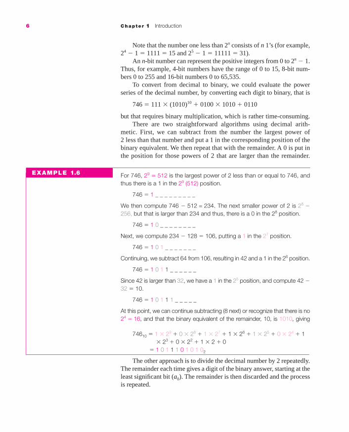
metic. First, we can subtract from the number the largest power of2 less than that number and put a 1 in the corresponding position of thebinary equivalent. We then repeat that with the remainder. A 0 is put inthe position for those powers of 2 that are larger than the remainder.
For 746, 29 � 512 is the largest power of 2 less than or equal to 746, andthus there is a 1 in the 29 (512) position.
746 � 1 _ _ _ _ _ _ _ _ _
We then compute 746 � 512 = 234. The next smaller power of 2 is 28 �
256, but that is larger than 234 and thus, there is a 0 in the 28 position.
746 � 1 0 _ _ _ _ _ _ _ _
Next, we compute 234 � 128 � 106, putting a 1 in the 27 position.
746 � 1 0 1 _ _ _ _ _ _ _
Continuing, we subtract 64 from 106, resulting in 42 and a 1 in the 26 position.
746 � 1 0 1 1 _ _ _ _ _ _
Since 42 is larger than 32, we have a 1 in the 25 position, and compute 42 �32 � 10.
746 � 1 0 1 1 1 _ _ _ _ _
At this point, we can continue subtracting (8 next) or recognize that there is no24 � 16, and that the binary equivalent of the remainder, 10, is 1010, giving
74610 � 1 � 29 � 0 � 28 � 1 � 27 � 1 � 26 � 1 � 25 � 0 � 24 � 1� 23 � 0 � 22 � 1 � 2 � 0
� 1 0 1 1 1 0 1 0 1 02
The other approach is to divide the decimal number by 2 repeatedly.The remainder each time gives a digit of the binary answer, starting at theleast significant bit (a0). The remainder is then discarded and the processis repeated.
6 Chapter 1 Introduction
EXAMPLE 1.6
mar91647_c01_001_028.qxd 10/22/08 11:33 AM Page 6

Converting 746 from decimal to binary, we compute746�2 � 373 with a remainder of 0 0373�2 � 186 with a remainder of 1 10186�2 � 93 with a remainder of 0 010
93�2 � 46 with a remainder of 1 101046�2 � 23 with a remainder of 0 0101023�2 � 11 with a remainder of 1 10101011�2 � 5 with a remainder of 1 1101010
5�2 � 2 with a remainder of 1 111010102�2 � 1 with a remainder of 0 0111010101�2 � 0 with a remainder of 1 1011101010
Do not forget the last division (1/2); it produces the most significant 1.We could continue dividing by 2 and get additional leading 0’s. Thus,the answer is 1011101010 as before. In this method, we could alsostop when we recognize the number that is left and convert it to binary.Thus, when we had 23, we could recognize that as 10111 (from Table 1.3)and place that in front of the bits we had produced, giving 10111 01010.
Convert 105 to binary105�2 � 52, rem 1 produces 1
52�2 � 26, rem 0 0126�2 � 13, rem 0 001
but 13 � 1101 1101 001
The method works because all of the terms in the power series except the last divide evenly by 2. Thus, since
746 � 1 � 29 � 0 � 28 � 1 � 27 � 1 � 26 � 1 � 25 � 0 � 24
� 1 � 23 � 0 � 22 � 1 � 2 � 0
746�2 � 373 and remainder of 0� 1 � 28 � 0 � 27 � 1 � 26 � 1 � 25 � 1 � 24
� 0 � 23 � 1 � 22 � 0 � 2 � 1 � rem 0
The last bit became the remainder. If we repeat the process, we get
373�2 � 186 and remainder of 1� 1 � 27 � 0 � 26 � 1 � 25 � 1 � 24 � 1 � 23 � 0 � 22
� 1 � 2 � 0 � rem 1
That remainder is the second digit from the right. On the next division,the remainder will be 0, the third digit. This process continues until themost significant bit is found.
1.2 A Brief Review of Number Systems 7
EXAMPLE 1.8
[SP 1, 2; EX 1, 2]*
*At the end of most sections, a list of solved problems and exercises that are appropriateto that section is given.
EXAMPLE 1.7
mar91647_c01_001_028.qxd 11/26/08 2:24 PM Page 7

1.2.1 Hexadecimal
Hexadecimal, often referred to as hex (r � 16) is another base that is com-monly used in computer documentation. It is just a shorthand notation for binary. In hexadecimal, binary digits are grouped in fours (starting at theleast significant). For example, an 8-bit number,
N � �b727 � b62
6 � b525 � b42
4� � �b323 � b22
2 � b121 � b0�
� 24 �b723 � b62
2 � b521 � b4� � �b32
3 � b222 � b12
1 � b0�� 16h1 � h0
where the h1 represent the hexadecimal digits and must fall in the range0 to 15. Each term in parentheses is just interpreted in decimal. If thebinary number does not have a multiple of four bits, leading 0’s areadded. The digits above 9 are represented by the first six letters of thealphabet (uppercase).
10 A
11 B
12 C
13 D
14 E
15 F
(from Examples 1.6 and 1.7)
10111010102 � 0010 1110 10102
� 2EA16
To convert from hex to decimal, we evaluate the power series.
2EA16 � 2 � 162 � 14 � 16 � 10� 512 � 224 � 10 � 74610
Finally, to convert from decimal to hex, repeatedly divide by 16,producing the hex digits as the remainder (or convert to binary and thengroup the bits as in Example 1.9).
746�16 � 46 rem 10 produces A
46�16 � 2 rem 14 EA
2�16 � 0 rem 2 2EA
8 Chapter 1 Introduction
EXAMPLE 1.9
EXAMPLE 1.10
EXAMPLE 1.11
[SP 3, 4; EX 3, 4]
mar91647_c01_001_028.qxd 10/22/08 11:33 AM Page 8

1.2.2 Binary Addition
A common operation required in computers and other digital systems isthe addition of two numbers. In this section, we will describe the processfor adding binary numbers.
To compute the sum of two binary numbers, say
0 1 1 0 60 1 1 1 �7
we add one digit at a time (as we do in decimal), producing a sum anda carry to the next bit. Just as we have an addition table for decimal,we need one for binary (but it is of course much shorter) (Table 1.4).A step-by-step addition is shown in Example 1.12 for adding 6 (0110)and 7 (0111).
First, the least significant bits (the rightmost bits) are added, producing asum of 1 and a carry of 0, as shown in brown.
0
0 1 1 0
0 1 1 1
1
Next, we must add the second digit from the right,0 � 1 � 1 � 0 � (1 � 1) � 0 � 10 � 10
(a sum of 0 and a carry of 1)
or (0 � 1) � 1 � 1 � 1 � 10(the order of addition does not matter).
That addition is highlighted in brown.
1 0
0 1 1 0
0 1 1 1
0 1
The final two additions then become
1 1 0 1
0 1 1 0 0 1 1 0
0 1 1 1 0 1 1 1
1 0 1 1 1 0 1
Notice that in the third bit of addition, we had three 1’s (the carry in plus thetwo digits). That produced a sum of 3 (11 in binary), that is, a sum bit of 1
1.2 A Brief Review of Number Systems 9
Table 1.4 Binary addition.
0 � 0 � 00 � 1 � 11 � 0 � 11 � 1 � 10 (2, or a sum of 0 and a
carry of 1 to the next bit)
EXAMPLE 1.12
mar91647_c01_001_028.qxd 10/22/08 11:33 AM Page 9

10 Chapter 1 Introduction
and a carry of 1. The answer, of course, comes to 13 (in decimal). In thiscase, the last addition produced a carry out of 0, and thus the answer was4-bits long. If the operands were larger (say, 13 � 5), the answer wouldrequire 5 bits as shown in the following addition, where the last carry iswritten as part of the sum. (This is, of course, no different from decimaladdition, where the sum of two 4-digit numbers might produce a 4- or5-digit result.)
1 0 1
1 1 0 1 1 3
0 1 0 1 5
1 0 0 1 0 1 8
In a computer with n-bit words, when an arithmetic operation pro-duces a result that is out of range [for example, addition of n-bit positiveintegers produces an (n � 1)-bit result], it is called overflow. With theaddition of 4-bit positive integers, overflow occurs when the sum isgreater than or equal to 16 (that is, 24). In the previous example, therewas overflow since the answer, 18, is greater than 15, the largest 4-bitpositive integer.
After the addition of the least significant bits (which only has twooperands), each remaining addition is a three-operand problem. We willdenote the carry that is added in as cin and the resulting carry from theaddition cout. The addition problem then becomes
cin
ab
cout s
Table 1.5 shows a truth table of the addition process.A device that does this 1-bit computation is referred to as a full
adder. To add 4-bit numbers, we might build four of these and connectthem as shown in Figure 1.2. Notice that the carry input of the bit 1 adder
Figure 1.2 A 4-bit adder.
FullAdder
c4 s4
FullAdder
s3
FullAdder
s2
FullAdder
a4 b4 a3 b3 a2 b2 a1 0c1 b1
c1s1
Table 1.5 One-bit adder.
a b cin cout s
0 0 0 0 00 0 1 0 10 1 0 0 10 1 1 1 01 0 0 0 11 0 1 1 01 1 0 1 01 1 1 1 1
[SP 5; EX 5]
mar91647_c01_001_028.qxd 10/22/08 11:33 AM Page 10

has a 0 on it, since there is no carry into that bit. Sometimes a simpler cir-cuit (called a half adder) is built for that bit. We will return to this prob-lem in Chapter 2, when we are prepared to design the full adder.
1.2.3 Signed Numbers
Up to this point, we have only considered positive integers, sometimesreferred to as unsigned numbers. Computers must deal with signed num-bers, that is, both positive and negative numbers. The human-friendlynotation is referred to as signed-magnitude (� 5 or � 3 as decimalexamples). This could be incorporated into a computer, using the first bitof a number as a sign indicator (normally 0 for positive and 1 for nega-tive) and the remaining bits for the magnitude. Thus, in a 4-bit system,we would represent
�5 → 0101 �5 → 1101 � 3 → 1011
With 3 bits for magnitude, the range of numbers available would be from�7 to �7. (Of course, most computers use a larger number of bits tostore numbers and thus have a much larger range.) Note that such arepresentation has both a positive (0000) and negative (1000) zero.Although that might cause confusion (or at least complicate the internallogic of the computer), the major problem with signed-magnitude is thecomplexity of arithmetic. Consider the following addition problems:
�5 �5 �5 �5 �3 �3�3 �3 �3 �3 �5 �5
�8 �8 �2 �2 �2 �2
In the first two, where the signs of the two operands are the same, wejust add the magnitudes and retain the sign. For these two, the computa-tion is 5 � 3. In each of the other examples, we must determine whichis the larger magnitude. (It could be the first operand or the second.)Then, we must subtract the smaller from the larger, and finally, attachthe sign of the larger magnitude. For these four, the computation is5 � 3. Although this could all be done, the complexity of the hardwareinvolved (an adder, a subtractor, and a comparator) has led to anothersolution.
Signed binary numbers are nearly always stored in two’s comple-ment format. The leading bit is still the sign bit (0 for positive). Positivenumbers (and zero) are just stored in normal binary. The largest numberthat can be stored is 2n � 1 � 1 (7 for n � 4). Thus, in a 4-bit system, �5would be stored as 0101.
The negative number, �a, is stored as the binary equivalent of 2n � ain an n-bit system. Thus, for example, �3 is stored as the binary for16 � 3 � 13, that is, 1101.
The most negative number that can be stored is �2n � 1 (�8 in a4-bit system). The largest number available in two’s complement isabout half that of unsigned numbers with the same number of bits, since
1.2 A Brief Review of Number Systems 11
mar91647_c01_001_028.qxd 10/22/08 11:33 AM Page 11

12 Chapter 1 Introduction
half of the 2n representations are used for negative numbers. This methodextends to other bases than binary. It is referred to as radix complement. Negative numbers, �a, in n digits are stored as r n � a. In decimal forexample, this is called ten’s complement. In a 2-digit decimal system,�16 would be stored as 100 � 16 � 84. (Numbers from 0 to 49 wouldbe considered positive and those between 50 and 99 would be represen-tations of negative numbers.)
An easier way to find the storage format for negative numbers intwo’s complement is the following three-step approach:
1. Find the binary equivalent of the magnitude.
2. Complement each bit (that is, change 0’s to 1’s and 1’s to 0’s)
3. Add 1.
�5 �1 �01. 5: 0 1 0 1 1: 0 0 0 1 0: 0 0 0 0
2. 1 0 1 0 1 1 1 0 1 1 1 13. 1 1 1
�5: 1 0 1 1 �1: 1 1 1 1 0 0 0 0
(a) (b) (c)
Note that there is no negative zero; the process of complementing �0 pro-duces an answer of 0000. In two’s complement addition, the carry out ofthe most significant bit is ignored.
Table 1.6 lists the meaning of all 4-bit numbers both as positive(unsigned) numbers and as two’s complement signed numbers.
To find the magnitude of a negative number stored in two’s comple-ment format (that is, one that begins with a 1), the second and third stepsof the negation process are followed.
�5: 1 0 1 1 �1: 1 1 1 1
2. Bit-by-bit complement 0 1 0 0 0 0 0 03. Add 1 1 1
5: 0 1 0 1 1: 0 0 0 1
(We could subtract 1 and then complement, instead; that will give the sameanswer.)
The reason that two’s complement is so popular is the simplicity ofaddition. To add any two numbers, no matter what the sign of each is, wejust do binary addition on their representations. Three sample computations
EXAMPLE 1.13
EXAMPLE 1.14
mar91647_c01_001_028.qxd 10/22/08 11:33 AM Page 12

are shown in Example 1.15. In each case, the carry out of the most sig-nificant bit is ignored.
�5 1 0 1 1 �5 1 0 1 1 �5 1 0 1 1
�7 0 1 1 1 �5 0 1 0 1 �3 0 0 1 1
�2 (1) 0 0 1 0 0 (1) 0 0 0 0 �2 (0) 1 1 1 0
In the first, the sum is 2. In the second, the sum is 0. In the third, the sum is�2, and, indeed, the representation of �2 is produced.
Overflow occurs when the sum is out of range. For 4-bit numbers,that range is �8 � sum � �7.
�5 0 1 0 1
�4 0 1 0 0
(0) 1 0 0 1 (looks like �7)
The answer produced is clearly wrong because the correct answer (�9) isout of range.
Indeed, whenever we add two positive numbers (each beginningwith a 0) and get a result that looks negative (begins with a 1), there isoverflow. Similarly, adding two negative numbers and obtaining a sum
1.2 A Brief Review of Number Systems 13
Table 1.6 Signed and unsigned 4-bit numbers.
SignedBinary Positive (two’s complement)
0000 0 00001 1 � 10010 2 � 20011 3 � 30100 4 � 40101 5 � 50110 6 � 60111 7 � 71000 8 � 81001 9 � 71010 10 � 61011 11 � 51100 12 � 41101 13 � 31110 14 � 21111 15 � 1
EXAMPLE 1.16
EXAMPLE 1.15
mar91647_c01_001_028.qxd 10/22/08 11:33 AM Page 13
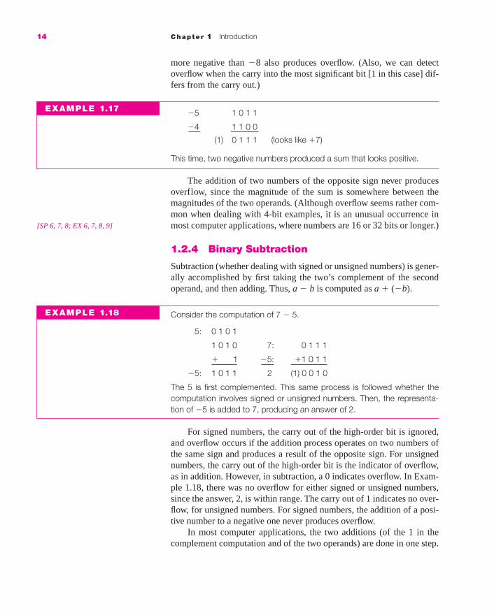
more negative than �8 also produces overflow. (Also, we can detectoverflow when the carry into the most significant bit [1 in this case] dif-fers from the carry out.)
�5 1 0 1 1
�4 1 1 0 0
(1) 0 1 1 1 (looks like �7)
This time, two negative numbers produced a sum that looks positive.
The addition of two numbers of the opposite sign never producesoverflow, since the magnitude of the sum is somewhere between themagnitudes of the two operands. (Although overflow seems rather com-mon when dealing with 4-bit examples, it is an unusual occurrence inmost computer applications, where numbers are 16 or 32 bits or longer.)
1.2.4 Binary Subtraction
Subtraction (whether dealing with signed or unsigned numbers) is gener-ally accomplished by first taking the two’s complement of the secondoperand, and then adding. Thus, a � b is computed as a � (�b).
Consider the computation of 7 � 5.
5: 0 1 0 1
1 0 1 0 7: 0 1 1 1
� 1 �5: �1 0 1 1
�5: 1 0 1 1 2 (1) 0 0 1 0
The 5 is first complemented. This same process is followed whether thecomputation involves signed or unsigned numbers. Then, the representa-tion of �5 is added to 7, producing an answer of 2.
For signed numbers, the carry out of the high-order bit is ignored,and overflow occurs if the addition process operates on two numbers ofthe same sign and produces a result of the opposite sign. For unsignednumbers, the carry out of the high-order bit is the indicator of overflow,as in addition. However, in subtraction, a 0 indicates overflow. In Exam-ple 1.18, there was no overflow for either signed or unsigned numbers,since the answer, 2, is within range. The carry out of 1 indicates no over-flow, for unsigned numbers. For signed numbers, the addition of a posi-tive number to a negative one never produces overflow.
In most computer applications, the two additions (of the 1 in thecomplement computation and of the two operands) are done in one step.
14 Chapter 1 Introduction
EXAMPLE 1.17
[SP 6, 7, 8; EX 6, 7, 8, 9]
EXAMPLE 1.18
mar91647_c01_001_028.qxd 10/22/08 11:33 AM Page 14

The least significant bit of the adder (bit 1) has a zero carry input foraddition. The 1 that was added in the process of complementing can beinput to that carry input for subtraction. Thus, to compute 7 � 5, we takethe bit-by-bit complement of 5 (0101 becomes 1010) and add.
7 � 5
1
0 1 1 1
1 0 1 0
(1) 0 0 1 0
Of course, we could design a subtractor (in addition to the adder),but that is unnecessary additional hardware for most computers.
Note that this process works for unsigned numbers even if the operandsare larger than could be represented in a two’s complement system, asshown in Example 1.20, where the difference 14 � 10 is computed.
1
1 1 1 0
�0 1 0 1
(1) 0 1 0 0 � 4
We see overflow for unsigned numbers in Example 1.21a and forsigned numbers in Example 1.21b.
5 � 7 7 � (�5)
1 1
0 1 0 1 0 1 1 1
1 0 0 0 0 1 0 0(0) 1 1 1 0 1 1 0 0
(a) (b)
For unsigned numbers, overflow is indicated by the carry of 0. The result of(a) should be negative (�2), which cannot be represented in an unsignedsystem. For signed numbers, the result is correct. For signed numbers,overflow may occur if we subtract a negative number from a positive one ora positive number from a negative one, as shown in Example 1.21b. That isoverflow because the addition process involved two positive numbers andthe result looked negative. (Indeed, the answer should be 12, but that isgreater than the largest 4-bit signed number, 7.)
1.2 A Brief Review of Number Systems 15
EXAMPLE 1.19
[SP 9, 10; EX 10]
EXAMPLE 1.20
EXAMPLE 1.21
mar91647_c01_001_028.qxd 10/22/08 11:33 AM Page 15

16 Chapter 1 Introduction
Table 1.7 Binary-coded decimal codes.
Decimal 8421 5421 2421 Excess 3 2 of 5digit code code code code code
0 0000 0000 0000 0011 110001 0001 0001 0001 0100 101002 0010 0010 0010 0101 100103 0011 0011 0011 0110 100014 0100 0100 0100 0111 011005 0101 1000 1011 1000 010106 0110 1001 1100 1001 010017 0111 1010 1101 1010 001108 1000 1011 1110 1011 001019 1001 1100 1111 1100 00011
unused 1010 0101 0101 0000 any of1011 0110 0110 0001 the 221100 0111 0111 0010 patterns1101 1101 1000 1101 with 0, 1,1110 1110 1001 1110 3, 4, or 51111 1111 1010 1111 1’s
*See Section 5.8.1 for an example of this.
1.2.5 Binary Coded Decimal (BCD)
Internally, most computers operate on binary numbers. However, whenthey interface with humans, the mode of communication is generallydecimal. Thus, it is necessary to convert from decimal to binary on inputand from binary to decimal on output. (It is straightforward to writesoftware to do this conversion.) However, even this decimal input andoutput must be coded into binary, digit by digit. If we use the first 10 binary numbers to represent the 10 decimal digits (as in the first binarycolumn in Table 1.7), then the number 739, for example, would bestored as
0111 0011 1001
Each decimal digit is represented by 4 bits, and thus a 3-digit decimalnumber requires 12 bits (whereas, if it were converted to binary, it wouldrequire only 10 bits because numbers up to 1023 can be represented with10 bits). In addition to the inefficiency of storage, arithmetic on BCDnumbers is much more complex* than that on binary, and thus BCD isonly used internally in small systems requiring limited computation.
We have already discussed the simplest code, using the first 10 binarynumbers to represent the 10 digits. The remaining 4-bit binary numbers
mar91647_c01_001_028.qxd 10/22/08 11:33 AM Page 16

(1010, 1011, 1100, 1101, 1110, 1111) are unused. This code, and those inthe next two columns of Table 1.7 are referred to as weighted codesbecause the value represented is computed by taking the sum of each digittimes its weight. This first code is referred to as the 8421 code, since thoseare the weights of the bits. Each decimal digit is represented by
8 � a3 � 4 � a2 � 2 � a1 � 1 � a0
It is also referred to as straight binary. Two other weighted codes (5421and 2421) that are occasionally used are shown next.
Two other codes that are not weighted are also shown in Table 1.7.The first is excess 3 (XS3) where the decimal digit is represented by thebinary equivalent of 3 more than the digit. For example, 0 is stored as thebinary 3 (0011) and 6 as the binary of 6 � 3 � 9 (1001). The final col-umn shows a 2 of 5 code, where each digit is represented by a 5-bit num-ber, two of which are 1 (and the remaining three bits are 0). This providessome error detection capabilities, because, if an error is made in just oneof the bits (during storage or transmission), the result will contain eitherone or three 1’s and can be detected as an error.
Note that in both the 5421 and 2421 codes, other combinations canbe used to represent some of the digits (such as 0101 for 5). However,those shown in the table are the standard representations; the others areincluded in the unused category.
Each of the representations has advantages in various applications.For example, if signed (ten’s complement) numbers were stored, thefirst digit of that number would be in the range 5 to 9 for negative num-bers. In the 5421, 2421, and excess 3 codes, that would correspond tothe first bit of the number being 1. (We would only need to check 1 bitto determine if a number is negative.) In the 8421 code, however, morecomplex logic is required, because the first bit might be either 0 or 1 fornegative numbers. In both 5421 and excess 3 codes, the ten’s comple-ment is computed by complementing each bit and adding 1 (as in two’scomplement). The process is more complex using the other codes. Wewill make use of some of these codes in later examples.
1.2.6 Other Codes
Other codes also appear in the digital world. Alphanumeric informationis transmitted using the American Standard Code for Information Inter-change (ASCII). Seven digits are used to represent the various characterson the standard keyboard as well as a number of control signals (such ascarriage return). Table 1.8 lists the printable codes. (Codes beginningwith 00 are for control signals.)
This allows us to code anything that can be printed from the stan-dard keyboard. For example, the word Logic would be coded
1.2 A Brief Review of Number Systems 17
[SP 11, 12; EX 11, 12]
mar91647_c01_001_028.qxd 12/16/08 2:32 PM Page 17

18 Chapter 1 Introduction
Table 1.9 Gray code.
Number Gray code Number Gray code
0 0000 8 11001 0001 9 11012 0011 10 11113 0010 11 11104 0110 12 10105 0111 13 10116 0101 14 10017 0100 15 1000
A Gray code is particularly useful in coding the position of a continuousdevice. As the device moves from one section to the next, only 1 bit ofthe code changes. If there is some uncertainty as to the exact position,only 1 bit is in doubt. If a normal binary code were used, all 4 bits wouldchange as it moved from 7 to 8.
1001100 1101111 1100111 1101001 1100011
L o g i c
Table 1.8 ASCII code.
a6a5a4
a3a2a1a0 010 011 100 101 110 111
0000 space 0 @ P ` p0001 ! 1 A Q a q0010 “ 2 B R b r0011 # 3 C S c s0100 $ 4 D T d t0101 % 5 E U e u0110 & 6 F V f v0111 ‘ 7 G W g w1000 ( 8 H X h x1001 ) 9 I Y i y1010 * : J Z j z1011 � ; K [ k {1100 , < L \ l |1101 � M ] m }1110 . > N ^ n ~1111 / ? O _ o delete
[SP 13; EX 13]
In a Gray code, consecutive numbers differ in only one bit. Table 1.9shows a 4-bit Gray code sequence.
mar91647_c01_001_028.qxd 10/22/08 11:33 AM Page 18

1.3 Solved Problems 19
1.3 SOLVED PROBLEMS
1. Convert the following positive binary integers to decimal.
a. 110100101
b. 00010111
a. 110100101 � 1 � 4 � 32 � 128 � 256 � 421Starting the evaluation from right (1’s position) to left(28 position). (There are 0’s in the 2, 8, 16, and 64 bits.)
b. 00010111 � 1 � 2 � 4 � 16 � 23
Leading 0’s do not change the result.
2. Convert the following decimal integers to binary. Assume allnumbers are unsigned (positive) and represented by 12 bits.
a. 47
b. 98
c. 5000
a. 47 47 � 64 Thus no 26 bit or greater
47 � 32 � 15 gives a 25 bit
15 � 16 no 24 bit
15 � 8 � 7 23 bit
7 � 111 thus last 3 bits are 111
47 � 000000101111
b. 98 98/2 � 49 remainder � 0 0
49/2 � 24 remainder � 1 10
24/2 � 12 remainder � 0 010
12/2 � 6 remainder � 0 0010
6/2 � 3 remainder � 0 00010
3/2 � 1 remainder � 1 100010
1/2 � 0 remainder � 1 1100010
We could keep dividing 0 by 2 and getting remainders of 0 until we had12 bits or recognize that the leading bits must be 0.
98 � 000001100010
As in part a, we could have stopped dividing when we recognizedthe number, say that 12 � 1100. We would take what we had alreadyfound, the three least significant bits of 010, and put the binary for 12ahead of that, getting the same answer, of course, 1100010 (with enoughleading 0’s to make up the appropriate number of bits).
c. 5000: cannot represent in 12 bits because 5000 212.
mar91647_c01_001_028.qxd 10/22/08 11:33 AM Page 19

20 Chapter 1 Introduction
3. Convert the following to hexadecimal
a. 110101101112
b. 61110
Leading 0’s are added when necessary to make the number of bits a mul-tiple of 4.
a. 0110 1011 0111 � 6B716
b. 611�16 � 38 rem 3 3
38�16 � 2 rem 6 63
2�16 � 0 rem 2 263
This equals 0010 0110 0011.
4. Convert the following hexadecimal integers to decimala. 263
b. 1C3
a. 3 � 6 � 16 � 2 � 162 � 3 � 96 � 512 � 611
b. 3 � 12 � 16 � 162 � 3 � 192 � 256 � 451
5. Compute the sum of the following pairs of 6-bit unsignedintegers. If the answer is to be stored in a 6-bit location, indicatewhich of the sums produces overflow. Also, show the decimalequivalent of each problem.
a. 0 0 1 0 1 1 � 0 1 1 0 1 0
b. 1 0 1 1 1 1 � 0 0 0 0 0 1
c. 1 0 1 0 1 0 � 0 1 0 1 0 1
d. 1 0 1 0 1 0 � 1 0 0 0 1 1
a. 0 1 0 0 1
11 0 0 1 0 1 1 0 0 1 0 1 1 0 0 1 0 1 1
26 0 1 1 0 1 0 0 1 1 0 1 0 0 1 1 0 1 0
37 1 0 1 1 0 1
1 0 1 1 1
0 0 1 0 1 1 0 0 1 0 1 1 0 0 1 0 1 1
0 1 1 0 1 0 0 1 1 0 1 0 0 1 1 0 1 0
0 1 0 1 0 0 1 0 1 0 1 0 0 1 0 1 � 37
Note that in this case the last carry result is 0 (it is shown as part of thesum) and thus the answer does fit in 6 bits (there is no overflow).
mar91647_c01_001_028.qxd 10/22/08 11:33 AM Page 20

b. 0 1 1 1 1 (carries)
1 0 1 1 1 1 47
0 0 0 0 0 1 1
0 1 1 0 0 0 0 48
c. 0 0 0 0 0
1 0 1 0 1 0 42
0 1 0 1 0 1 21
0 1 1 1 1 1 1 63
d. 0 0 0 1 0
1 0 1 0 1 0 42
1 0 0 0 1 1 35
1 0 0 1 1 0 1 77 overflow (looks like 13)
Note that the answer is larger than 63, which is the largest 6-bitnumber.
6. The following decimal numbers are to be stored in a 6-bit two’scomplement format. Show how they are stored.
a. � 14
b. � 20
c. � 37
a. �14 � 001110 Positive numbers are just converted to binary.
b. �20: �20 � 010100
Complement every bit 1 0 1 0 1 1
Add 1 1
�20 is stored as 1 0 1 1 0 0
c. �37: Cannot be stored, the range of 6-bit numbers is �32 � n � 31. Converting 37 to binary would give 100101,but that represents a negative number.
7. The following 6-bit two’s complement numbers were found in acomputer. What decimal number do they represent?
a. 001011
b. 111010
a. 001011: Because it begins with 0, it is positive � 1 � 2 � 8 � 11
b. 111010: Because it begins with a 1, it is negative; take two’scomplement: 0 0 0 1 0 1
1
0 0 0 1 1 0 � 6
Thus, 111010 represents �6.
1.3 Solved Problems 21
mar91647_c01_001_028.qxd 10/22/08 11:33 AM Page 21

8. Each of the following pairs of signed (two’s complement)numbers are stored in computer words (6 bits). Compute the sumas it is stored in a 6-bit computer word. Show the decimalequivalents of each operand and the sum. Indicate if there isoverflow.
a. 1 1 1 1 1 1 � 0 0 1 0 1 1
b. 0 0 1 0 0 1 � 1 0 0 1 0 0
c. 0 0 1 0 0 1 � 0 1 0 0 1 1
d. 0 0 1 0 1 0 � 0 1 1 0 0 0
e. 1 1 1 0 1 0 � 1 1 0 0 0 1
f. 1 0 1 0 0 1 � 1 1 0 0 0 1
g. 1 1 0 1 0 1 � 0 0 1 0 1 1
a. 1 1 1 1 1 1 �1
0 0 1 0 1 1 �11 The carry out is ignored and will not
(1) 0 0 1 0 1 0 �10 be shown in the remaining examples.
b. 0 0 1 0 0 1 �9
1 0 0 1 0 0 �28
1 0 1 1 0 1 �19
c. 0 0 1 0 0 1 �9
0 1 0 0 1 1 �19
0 1 1 1 0 0 �28
d. 0 0 1 0 1 0 �10
0 1 1 0 0 0 �24
1 0 0 0 1 0 looks like �30; should be �34; overflowsum of two positive numbers looks negative
e. 1 1 1 0 1 0 �6
1 1 0 0 0 1 �15
1 0 1 0 1 1 �21
f. 1 0 1 0 0 1 �23
1 1 0 0 0 1 �15
0 1 1 0 1 0 looks like �26; should be � 38; overflowsum of two negative numbers looks positive
g. 1 1 0 1 0 1 �11
0 0 1 0 1 1 �11
0 0 0 0 0 0 0
9. Subtract each of the following pairs of unsigned integers.
a. 0 0 1 1 0 1 � 0 0 0 1 1 0
b. 1 1 0 1 0 1 � 0 0 0 0 1 1
c. 0 0 0 1 1 1 � 0 1 0 0 1 1
22 Chapter 1 Introduction
mar91647_c01_001_028.qxd 10/22/08 11:33 AM Page 22
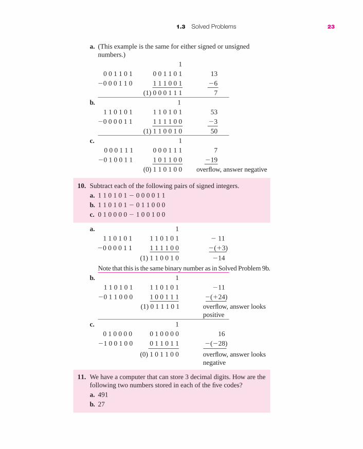
a. (This example is the same for either signed or unsignednumbers.)
1
0 0 1 1 0 1 0 0 1 1 0 1 13
�0 0 0 1 1 0 1 1 1 0 0 1 �6
(1) 0 0 0 1 1 1 7
b. 1
1 1 0 1 0 1 1 1 0 1 0 1 53
�0 0 0 0 1 1 1 1 1 1 0 0 �3
(1) 1 1 0 0 1 0 50
c. 1
0 0 0 1 1 1 0 0 0 1 1 1 7
�0 1 0 0 1 1 1 0 1 1 0 0 �19
(0) 1 1 0 1 0 0 overflow, answer negative
10. Subtract each of the following pairs of signed integers.
a. 1 1 0 1 0 1 � 0 0 0 0 1 1
b. 1 1 0 1 0 1 � 0 1 1 0 0 0
c. 0 1 0 0 0 0 � 1 0 0 1 0 0
a. 1
1 1 0 1 0 1 1 1 0 1 0 1 � 11
�0 0 0 0 1 1 1 1 1 1 0 0 �(�3)
(1) 1 1 0 0 1 0 �14
Note that this is the same binary number as in Solved Problem 9b.
b. 1
1 1 0 1 0 1 1 1 0 1 0 1 �11
�0 1 1 0 0 0 1 0 0 1 1 1 �(�24)
(1) 0 1 1 1 0 1 overflow, answer lookspositive
c. 1
0 1 0 0 0 0 0 1 0 0 0 0 16
�1 0 0 1 0 0 0 1 1 0 1 1 �(�28)
(0) 1 0 1 1 0 0 overflow, answer looksnegative
11. We have a computer that can store 3 decimal digits. How are thefollowing two numbers stored in each of the five codes?
a. 491
b. 27
1.3 Solved Problems 23
mar91647_c01_001_028.qxd 10/22/08 11:33 AM Page 23
a. 8421 0100 1001 00015421 0100 1100 00012421 0100 1111 0001XS3 0111 1100 01002 of 5 01100 00011 10100Note that the first four codes require 12-bit words; the 2 of 5code requires 15-bit words.
b. 8421 0000 0010 01115421 0000 0010 10102421 0000 0010 1101XS3 0011 0101 10102 of 5 11000 10010 00110
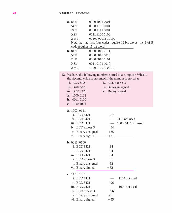
12. We have the following numbers stored in a computer. What isthe decimal value represented if the number is stored as
i. BCD 8421 iv. BCD excess 3ii. BCD 5421 v. Binary unsigned
iii. BCD 2421 vi. Binary signeda. 1000 0111b. 0011 0100c. 1100 1001
a. 1000 0111i. BCD 8421 87ii. BCD 5421 — 0111 not used
iii. BCD 2421 — 1000, 0111 not usediv. BCD excess 3 54v. Binary unsigned 135vi. Binary signed �121
b. 0011 0100i. BCD 8421 34
ii. BCD 5421 34iii. BCD 2421 34iv. BCD excess 3 01v. Binary unsigned 52
vi. Binary signed �52
c. 1100 1001i. BCD 8421 — 1100 not used
ii. BCD 5421 96iii. BCD 2421 — 1001 not usediv. BCD excess 3 96v. Binary unsigned 201
vi. Binary signed �55
24 Chapter 1 Introduction
mar91647_c01_001_028.qxd 10/22/08 11:33 AM Page 24

13. a. Code the following into ASCII.
i. HELLO
ii. hello
b. Translate the following into English.
i. 1011001 1100101 1110011 0100001
ii. 0110010 0101011 0110001 0111101 0110011
a. i. 1001000 1000101 1001100 1001100 1001111
ii. 1101000 1100101 1101100 1101100 1101111
b. i. Yes!
ii. 2�1�3
1.4 EXERCISES*1. Convert the following unsigned binary integers to decimal.
★a. 11111 e. 10101010
b. 1000000 f. 000011110000
c. 1001101101 g. 110011001100★ d. 101111 ★ h. 000000000000
2. Convert the following decimal integers to binary. Assume allnumbers are unsigned (positive) and represented by 12 bits.★a. 73 c. 402 ★e. 1000 ★g. 4200
b. 127 d. 512 f. 17 h. 1365
3. Convert the following to hexadecimal★a. 1001011010112
b. 101101000001012★c. 79110
d. 160010
4. Convert the following hexadecimal numbers to decimal
a. 1000
b. ABCD★c. 3FF
5. Compute the sum of the following pairs of 6-bit unsigned integers.If the answer is to be stored in a 6-bit location, indicate which ofthe sums produce overflow. Also, show the decimal equivalent ofboth operands and the result.★a. 000011 � 001100 ★e. 001011 � 100111
b. 010100 � 101101 f. 000101 � 000111
c. 011100 � 011010 g. 101100 � 100100★d. 110011 � 001110
1.4 Exercises 25
*Answers to Exercises marked with a star (★) are given in Appendix B.
EX
ER
CIS
ES
mar91647_c01_001_028.qxd 10/22/08 11:33 AM Page 25

26 Chapter 1 Introduction
6. The following decimal integers are to be stored in a 6-bit two’scomplement format. Show how they are stored.★a. �25 ★c. �32 ★e. �15 g. �1
b. 0 d. �15 f. �45 h. �16
7. The following 6-bit two’s complement integers were found in acomputer. What decimal number do they represent?
a. 000101 ★c. 010101 e. 011111 g. 101010
b. 111111 ★d. 100100 f. 111001 ★h. 100000
8. We have a computer that stores binary signed integers in two’scomplement form. All numbers are 8 bits long.
a. What decimal number is represented by 01101011?
b. What decimal number is represented by 10101110?★c. How is the number �113 stored?★d. How is the number �143 stored?
e. How is the number �43 stored?
f. How is the number �43 stored?
9. Each of the following pairs of signed (two’s complement) integersare stored in computer words (6 bits). Compute the sum as it isstored in a 6-bit computer word. Show the decimal equivalents ofeach operand and the sum. Indicate if there is overflow.★a. 110101 c. 001100 e. 011010
001111 110100 001100
b. 111010 ★d. 101010 ★f. 111101
000111 100110 110000
10. For each of the following pairs of integers, subtract the secondfrom the first. Show the operands and the answers in decimal,assuming
i. the numbers are unsigned.
ii. the numbers are signed (two’s complement).
Indicate overflow where appropriate.
a. 010101 ★c. 111010 e. 110010
001100 000111 110111★b. 010001 ★d. 100100 f. 111010
011000 011000 101101
11. We have a computer that can store 3 decimal digits. How are eachof the following numbers stored in each of the five codes?
i. 8421 iv. excess 3
ii. 5421 v. 2 of 5
iii. 2421★a. 103 b. 999 c. 1 d. 0
EX
ER
CIS
ES
mar91647_c01_001_028.qxd 12/16/08 2:32 PM Page 26

12. We have the following numbers stored in a computer. What is thedecimal value represented if the number is stored as
i. BCD 8421 iv. BCD excess 3ii. BCD 5421 v. binary unsigned
iii. BCD 2421 vi. binary signed
a. 1111 1010 ★d. 1001 0101★b. 0001 1011 e. 1110 1101c. 1000 0011 f. 0100 1000
13. a. Code the following into ASCII
i. Problem 5 iii. 2 � 1 � 3★ii. “OK” iv. ABM
b. Translate the following into English
i. 1000001 1101100 1100001 1101110ii. 0100100 0110111 0101110 0111001 0110101
★iii. 0111001 0101111 0110011 0111101 0110011iv. 1010100 1101000 1100101 0100000 1100101
1101110 1100100
1.5 CHAPTER 1 TEST (30 MINUTES)*
1. Convert the decimal number 347 toa. binary.b. hexadecimal.Show your work.
2. Add the two unsigned binary numbers; show both operands and theresult in decimal as well as binary. (Be sure to show the carry asyou add.) Indicate if there is overflow.
0 1 0 1 1 1 0 1 0 1 1
0 1 1 1 0 0 1 1 0 0 1
3. Show the decimal equivalent of each of the numbers if they areinterpreted as (six answers).
1 0 0 1 0 1 0 1 0 1 1 1 0 0 1 1
a. Unsigned binary
b. Signed binary
c. BCD (8421 code)
1.5 Chapter 1 Test 27
*Tests assume students are allowed one sheet of 81–2
� 11 paper with any notes they wishon both sides. Solutions to Chapter Tests are given in Appendix C.
EX
ER
CIS
ES
CH
AP
TE
R T
ES
T
mar91647_c01_001_028.qxd 10/22/08 11:33 AM Page 27

28 Chapter 1 Introduction
4. Add the three pairs of signed (two’s complement) numbers. Be sure toshow the carry as you add. Show both operands and the result of eachaddition in decimal as well as binary. Indicate if there is overflow.
1 1 0 0 1 0 1 0 0 1 0 1
1 1 0 1 0 1 1 1 0 0 1 1
5. Subtract the two pairs of numbers. Show the operands and theresults in decimal and binary
a. assuming they are unsigned.
b. assuming they are signed.
1 1 0 1 � 1 1 0 0 1 0 1 0 � 0 1 1 0
Indicate if there is overflow.
CH
AP
TE
R T
ES
T
mar91647_c01_001_028.qxd 10/22/08 11:33 AM Page 28

CombinationalSystems
In this chapter, we will develop the tools to specify combinationalsystems. Then, we will develop an algebraic approach for thedescription of these systems, their simplification, and their imple-
mentation. We will concentrate on rather small systems, which will enable us to better understand the process. We will look at larger prob-lems in Chapter 5.
2.1 THE DESIGN PROCESS FORCOMBINATIONAL SYSTEMS
In this section, we will outline the process to be used to design combina-tional systems. (A similar process will be developed in Chapter 7 forsequential systems.) The design process typically starts with a problemstatement, a verbal description of the intended system. The goal is todevelop a block diagram of that system, utilizing available componentsand meeting the design objectives and constraints.
We will use the following five examples to illustrate the steps in thedesign process and, indeed, continue to follow some of them in subse-quent chapters, as we develop the tools necessary to do that design.
Continuing Examples (CE)
CE1. A system with four inputs, A, B, C, and D, and one output, Z, suchthat Z � 1 iff three of the inputs are 1.
CE2. A single light (that can be on or off) that can be controlled by any oneof three switches. One switch is the master on/off switch. If it is down, thelight is off. When the master switch is up, a change in the position of one ofthe other switches (from up to down or from down to up) will cause the lightto change state.
CE3. A system to do 1 bit of binary addition. It has three inputs (the 2 bitsto be added plus the carry from the next lower order bit) and produces twooutputs: a sum bit and a carry to the next higher order position.
29
C H A P T E R
2
mar91647_c02_029_110.qxd 10/22/08 12:56 PM Page 29

CE4. A display driver; a system that has as its input the code for a decimaldigit and produces as its output the signals to drive a seven-segment dis-play, such as those on most digital watches and numeric displays (morelater).
CE5. A system with nine inputs, representing two 4-bit binary numbers anda carry input, and one 5-bit output, representing the sum. (Each input num-ber can range from 0 to 15; the output can range from 0 to 31.)
In addition to these continuing examples, Appendix E will containsome complete examples of the design of small systems, from the verbaldescription through the design with gates. (There will also be some examples of sequential systems.)
The design process involves each of the following steps (althoughsome may not be necessary in some problems).
Sometimes, as in CE1, 3, and 5, the problem statement is alreadygiven in terms of binary inputs and outputs. Other times, it is up to the designer. In CE2, we need to create a numeric equivalence for each of theinputs and outputs. We might code the light on as a 1 output and off as 0.(We could just as well have used the opposite definition, as long as we arecoordinated with the light designer.) Similarly, we will define a switch inthe up position as a 1 input and down as 0. For CE4, the input is a decimaldigit. We must determine what BCD code is to be used. That might beprovided for us by whoever is providing the input, or we may have theability to specify it in such a way as to make our system simplest. We mustalso code the output; we need to know the details of the display andwhether a 1 or a 0 lights each segment. (We will discuss those details inSection 2.1.1.) In general, the different input and output representationsmay result in a significant difference in the amount of logic required.
This step is listed here because sometimes it is possible to dothis after having developed the truth table and sometimes, we must reallybreak up the problem before we can even begin to do such a table.
It is not possible to apply most of the design techniques that wewill develop to very large problems. Even CE5, the 4-bit adder, hasnine inputs and would thus require a truth table of 29 � 512 rows withnine input columns and five output columns. Although we can easilyproduce the entries for any line of that table, the table would spreadover several pages and be very cumbersome. Furthermore, the mini-mization techniques of this chapter and Chapter 3 would be strained.The problem becomes completely unmanageable if we go to a realistic
Step 1.5: If necessary, break the problem into smaller subproblems.
Step 1: Represent each of the inputs and outputs in binary.
30 Chapter 2 Combinational Systems
mar91647_c02_029_110.qxd 10/22/08 12:56 PM Page 30

2.1 The Design Process for Combinational Systems 31
adder for a computer—say one that adds 32-bit numbers. There thetable would be 264 lines long, even without a carry input (approxi-mately 1.84 � 1019). (That means that if we were to write 1 millionlines on each page and put 1 million pages in a book, we would stillneed over 18 million volumes to list the entire truth table. Or, if we hada computer that could process 1 billion lines of the truth table per sec-ond (requiring a supercomputer), it would still take over 584 years toprocess the whole table.)
Obviously, we have been able to solve such problems. In the case ofthe adder, we can imitate how we do it by hand, namely, add 1 bit at atime, producing 1 bit of the sum and the carry to the next bit. That is theproblem proposed in CE3; it only requires an eight-line truth table. Wecan build 32 such systems and connect them together.
Also, it is often most economical to take advantage of subsystemsthat already have been implemented. For example, we can buy the 4-bitadder described in CE5 (on a single integrated circuit chip). We mightwant to use that as a component in our design. We will examine this partof the design process further in Chapter 5.
We will concentrate on the idea of a truth table here and leave thedevelopment of algebraic expressions for later in the chapter. The truthtable format is the most common result of step 2 of the design process.We can do this in a digital system because each of the inputs only takeson one of two values (0 or 1). Thus, if we have n inputs, there are 2n inputcombinations and thus the truth table has 2n rows. These rows are nor-mally written in the binary order of the inputs (if, for no other reason,than to make sure that we do not leave any out). The truth table has twosets of columns: n input columns, one for each input variable, and m out-put columns, one for each of the m outputs.
An example of a truth table with two inputs, A and B, and one out-put, Y, is shown as Table 2.1, where there are two input columns, one out-put column, and 22 � 4 rows (not including the title row). We will lookat truth tables for some of the continuing examples shortly, after present-ing the other steps of the design process.
The truth table will lead directly to an implementation in some tech-nologies (see, for example, the ROM in Chapter 5). More often, we mustconvert that to an algebraic form to implement it. But the algebraic formwe get from the truth table tends to lead to rather complex systems. Thus,we will develop techniques for reducing the complexity of algebraicexpressions in this chapter and the next.
Step 3: Simplify the description.
Step 2: Formalize the design specification either in the form of atruth table or of an algebraic expression.
Table 2.1 A two-inputtruth table.
A B Y
0 0 00 1 11 0 11 1 1
mar91647_c02_029_110.qxd 10/22/08 12:56 PM Page 31
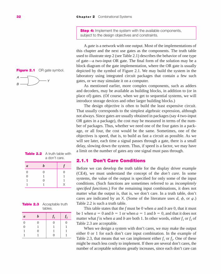
32 Chapter 2 Combinational Systems
A gate is a network with one output. Most of the implementations ofthis chapter and the next use gates as the components. The truth tableused to illustrate step 2 (see Table 2.1) describes the behavior of one typeof gate—a two-input OR gate. The final form of the solution may be ablock diagram of the gate implementation, where the OR gate is usuallydepicted by the symbol of Figure 2.1. We may build the system in thelaboratory using integrated circuit packages that contain a few suchgates, or we may simulate it on a computer.
As mentioned earlier, more complex components, such as addersand decoders, may be available as building blocks, in addition to (or inplace of) gates. (Of course, when we get to sequential systems, we willintroduce storage devices and other larger building blocks.)
The design objective is often to build the least expensive circuit.That usually corresponds to the simplest algebraic expression, althoughnot always. Since gates are usually obtained in packages (say 4 two-inputOR gates in a package), the cost may be measured in terms of the num-ber of packages. Thus, whether we need one of the four gates in a pack-age, or all four, the cost would be the same. Sometimes, one of theobjectives is speed, that is, to build as fast a circuit as possible. As wewill see later, each time a signal passes through a gate, there is a smalldelay, slowing down the system. Thus, if speed is a factor, we may havea limit on the number of gates any one signal must pass through.
2.1.1 Don’t Care Conditions
Before we can develop the truth table for the display driver example(CE4), we must understand the concept of the don’t care. In somesystems, the value of the output is specified for only some of the inputconditions. (Such functions are sometimes referred to as incompletelyspecified functions.) For the remaining input combinations, it does notmatter what the output is, that is, we don’t care. In a truth table, don’tcares are indicated by an X. (Some of the literature uses d, f, or w.)Table 2.2 is such a truth table.
This table states that the f must be 0 when a and b are 0, that it mustbe 1 when a � 0 and b � 1 or when a � 1 and b � 0, and that it does notmatter what f is when a and b are both 1. In other words, either f1 or f2 ofTable 2.3 are acceptable.
When we design a system with don’t cares, we may make the outputeither 0 or 1 for each don’t care input combination. In the example ofTable 2.3, that means that we can implement either f1 or f2. One of thesemight be much less costly to implement. If there are several don’t cares, thenumber of acceptable solutions greatly increases, since each don’t care can
Step 4: Implement the system with the available components,subject to the design objectives and constraints.
Figure 2.1 OR gate symbol.
A
BY
Table 2.2 A truth table witha don’t care.
a b f
0 0 00 1 11 0 11 1 X
Table 2.3 Acceptable truthtables.
a b f1 f2
0 0 0 00 1 1 11 0 1 11 1 0 1
mar91647_c02_029_110.qxd 10/22/08 12:56 PM Page 32

2.1 The Design Process for Combinational Systems 33
We will see a third kind of don’t care in CE4; we may really not carewhat one output is.
2.1.2 The Development of Truth Tables
Given a word problem, the first step is to decide how to code the inputs.Then, the development of a truth table is usually rather straightforward.The number of inputs determines the number of rows, and the majorproblem generally revolves about the ambiguity of English (or any natu-ral language).
For CE1, a 16-row truth table is required. There are four inputcolumns and one output column. (In Table 2.4, three output columns areshown Z1, Z2, and Z3 to account for the three interpretations of the prob-lem statement.) There is little room for controversy on the behavior ofthe system for the first 15 rows of the table. If there are fewer than three1’s on the input lines, the output is 0. If three of the inputs are 1 and theother is 0, then the output is 1. The only question in completing the tableis in relation to the last row. Does “three of the inputs are 1” mean exactlythree or does it mean at least three? If the former is true, then the last lineof the truth table is 0, as shown for Z1. If the latter is true, then the lastline of the table is 1, as shown in Z2. Two other options, both shown asZ3, are that we know that all four inputs will not be 1 simultaneously, and
Figure 2.2 Design example with don’t cares.
SystemOne
A J
KSystem
TwoB
C
be either 0 or 1, independently. The techniques we develop in Chapter 3 han-dle don’t cares very easily; they do not require solving separate problems.
In real systems, don’t cares occur in several ways. First, there maybe some input combinations that never occur. That is the case in CE4,where the input is the code for a decimal digit; there are only 10 possibleinput combinations. If a 4-bit code is used, then six of the input combi-nations never occur. When we build a system, we can design it such thatthe outputs would be either 0 or 1 for each of these don’t care combina-tions, since that input never happens.
A second place where don’t cares occur is in the design of one sys-tem to drive a second system. Consider the block diagram of Figure 2.2.We are designing System One to make System Two behave in a certainway. On some occasions, for certain values of A, B, and C, System Twowill behave the same way whether J is 0 or 1. In that case, the output J ofSystem One is a don’t care for that input combination. We will see thisbehavior arise in Chapter 7, where System Two is a flip flop (a binarystorage device).
mar91647_c02_029_110.qxd 10/22/08 12:56 PM Page 33
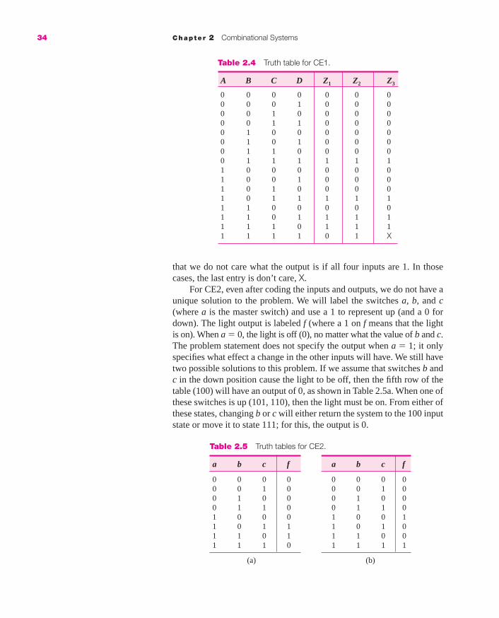
34 Chapter 2 Combinational Systems
that we do not care what the output is if all four inputs are 1. In thosecases, the last entry is don’t care, X.
For CE2, even after coding the inputs and outputs, we do not have aunique solution to the problem. We will label the switches a, b, and c(where a is the master switch) and use a 1 to represent up (and a 0 fordown). The light output is labeled f (where a 1 on f means that the lightis on). When a � 0, the light is off (0), no matter what the value of b and c.The problem statement does not specify the output when a � 1; it onlyspecifies what effect a change in the other inputs will have. We still havetwo possible solutions to this problem. If we assume that switches b andc in the down position cause the light to be off, then the fifth row of thetable (100) will have an output of 0, as shown in Table 2.5a. When one ofthese switches is up (101, 110), then the light must be on. From either ofthese states, changing b or c will either return the system to the 100 inputstate or move it to state 111; for this, the output is 0.
Table 2.5 Truth tables for CE2.
a b c f a b c f
0 0 0 0 0 0 0 00 0 1 0 0 0 1 00 1 0 0 0 1 0 00 1 1 0 0 1 1 01 0 0 0 1 0 0 11 0 1 1 1 0 1 01 1 0 1 1 1 0 01 1 1 0 1 1 1 1
(a) (b)
Table 2.4 Truth table for CE1.
A B C D Z1 Z2 Z3
0 0 0 0 0 0 00 0 0 1 0 0 00 0 1 0 0 0 00 0 1 1 0 0 00 1 0 0 0 0 00 1 0 1 0 0 00 1 1 0 0 0 00 1 1 1 1 1 11 0 0 0 0 0 01 0 0 1 0 0 01 0 1 0 0 0 01 0 1 1 1 1 11 1 0 0 0 0 01 1 0 1 1 1 11 1 1 0 1 1 11 1 1 1 0 1 X
mar91647_c02_029_110.qxd 10/22/08 12:56 PM Page 34

2.1 The Design Process for Combinational Systems 35
We could have started with some other fixed value, such as switchesb and c up means that the light is on or that switches b and c down meansthat the light is on. Either of these would produce the truth table of Table 2.5b, which is equally acceptable.
We have already developed the truth table for CE3, the 1-bit binaryfull adder, in Section 1.2.2, Table 1.5 (although we did not refer to it as atruth table at that time).
Although we could easily construct a truth table for CE5, the 4-bitadder, we would need 512 rows. Furthermore, once we had done this, wewould still find it nearly impossible to simplify the function by hand (thatis, without the aid of a computer). We will defer further discussion of thisproblem to Chapter 5.
We will now examine the display driver of CE4. A block diagram ofthe system is shown in Figure 2.3a. The inputs are a code for the decimaldigit and are labeled W, X, Y, and Z. The display driver must provide theseven inputs to the display, a, b, c, d, e, f, and g. The layout of the displayis shown in Figure 2.3b. How each digit is displayed is shown in Figure2.3c, where a solid line indicates that the segment is lit, and a dashed linethat it is not lit. Note that various devices use alternative displays for thedigits 6, 7, and 9. For example, segment a is sometimes lit for a 6, andsometimes it is not.
The first thing that we must do is to select a code for the decimaldigit. That will (obviously) affect the truth table and might make a sig-nificant difference in the cost of the implementation. For the sake of thisexample, we will assume that the digits are stored in 8421 code. (We willlook at variations on this in Chapter 4.) The next thing we need to knowis whether the display requires a 0 or a 1 on each segment input to lightthat segment. Both types of displays exist. The design specification mustalso indicate which of the alternative displays for 6, 7, and 9 should beused, or state that it doesn’t matter. Finally, we must decide what to do
Figure 2.3 A seven-segment display.
a
DisplayDriver
W
X
Y
Z
a
gf b
e c
d
dc
b
efg
(a) (b)
(c)
mar91647_c02_029_110.qxd 10/22/08 12:56 PM Page 35

Table 2.6 A truth table for the seven-segment display driver.
Digit W X Y Z a b c d e f g
0 0 0 0 0 1 1 1 1 1 1 01 0 0 0 1 0 1 1 0 0 0 02 0 0 1 0 1 1 0 1 1 0 13 0 0 1 1 1 1 1 1 0 0 14 0 1 0 0 0 1 1 0 0 1 15 0 1 0 1 1 0 1 1 0 1 16 0 1 1 0 X 0 1 1 1 1 17 0 1 1 1 1 1 1 0 0 X 08 1 0 0 0 1 1 1 1 1 1 19 1 0 0 1 1 1 1 X 0 1 1– 1 0 1 0 X X X X X X X– 1 0 1 1 X X X X X X X– 1 1 0 0 X X X X X X X– 1 1 0 1 X X X X X X X– 1 1 1 0 X X X X X X X– 1 1 1 1 X X X X X X X
EXAMPLE 2.1
a b c w x y z
0 0 0 0 1 1 10 0 1 1 1 0 10 1 0 X X X X0 1 1 1 1 1 11 0 0 0 0 1 01 0 1 X X X X1 1 0 0 1 1 01 1 1 1 1 1 0
36 Chapter 2 Combinational Systems
We want to develop a truth table for a system with three inputs, a, b, and c,and four outputs, w, x, y, z. The output is a binary number equal to thelargest integer that meets the input conditions:
a � 0: odd a � 1: even
b � 0: prime b � 1: not prime
c � 0: less than 8 c � 1: greater than or equal to 8
Some inputs may never occur; the output is never all 0’s.(A prime is a number that is only evenly divisible by itself and 1.) The follow-ing is a truth table for this system.
about the inputs that do not correspond to a decimal digit (1010, 1011,… , 1111). If we know for sure that they will never happen, then we don’tcare what the display driver produces for those input combinations. Onthe other hand, the specifications might state that the display is to beblank (no segment lit) or that it is to display an error code.
The truth table of Table 2.6 assumes 8241 code, a 1 to light a seg-ment, the version of 6, 7, and 9 does not matter, and that the inputs thatdo not represent a decimal digit never occur.
mar91647_c02_029_110.qxd 10/22/08 12:56 PM Page 36

2.2 Switching Algebra 37
For the first four rows, we are looking for odd numbers. The odd primesare 1, 3, 5, 7, 11, and 13. Thus, the first row is the binary for 7 (the largest oddprime less than 8) and the second row is the binary for 13. The next two rowscontain nonprimes. All odd numbers less than 8 are prime; therefore, theinput is never 010 and the outputs are don’t cares. Finally, 9 and 15 are oddnonprimes; 15 is larger. For the second half of the table, the only even primeis 2; thus, 101 never occurs. The largest even nonprimes are 6 and 14.
2.2 SWITCHING ALGEBRA
In the last section, we went from a verbal description of a combinationalsystem to a more formal and exact description—a truth table. Althoughthe truth table is sufficient to implement a system using read-only mem-ory (see Chapter 5), we need an algebraic description to analyze anddesign systems with other components. In this section, we will developthe properties of switching algebra.
We need the algebra for several reasons. Perhaps the most obvious isthat if we are presented with a network of gates, we need to obtain aspecification of the output in terms of the input. Since each gate isdefined by an algebraic expression, we most often need to be able tomanipulate that algebra. (We could try each possible input combinationand follow the signals through each gate until we reached the output.That, however, is a very slow approach to creating a whole truth table fora system of gates.)
Second, in the design process, we often obtain an algebraic expres-sion that corresponds to a much more complex network of gates than isnecessary. Algebra allows us to simplify that expression, perhaps evenminimize the amount of logic needed to implement it. When we move onto Chapter 3, we will see that there are other nonalgebraic ways of doingthis minimization, methods that are more algorithmic. However, it is stillimportant to understand the algebraic foundation behind them.
Third, algebra is often indispensable in the process of implementingnetworks of gates. The simplest algebraic expression, found by one of thetechniques presented in this chapter or the next, does not always correspondto the network that satisfies the requirements of the problem. Thus, we mayneed the algebra to enable us to satisfy the constraints of the problem.
In an earlier edition, we introduced the Karnaugh map in the middleof this chapter, to aid in the understanding of the algebraic manipulation.Without loss of continuity, one might study Section 3.1 before Sec-tion 2.7 and then refer to some examples in Appendix A, which illustratethe algebra using the map.
One approach to the development of switching algebra is to beginwith a set of postulates or axioms that define the more general Booleanalgebra. In Boolean algebra, each variable—inputs, outputs, and internalsignals—may take on one of k values (where k � 2). Based on these
[SP 1, 2; EX 1, 2]
mar91647_c02_029_110.qxd 10/22/08 12:56 PM Page 37

38 Chapter 2 Combinational Systems
postulates, we can define an algebra and eventually determine the mean-ing of the operators. We can then limit them to the special case of switch-ing algebra, k � 2. We have deferred a brief discussion of that approachto Section 2.9. Rather, we will define switching algebra in terms of itsoperators and a few basic properties.
2.2.1 Definition of Switching Algebra
Switching algebra is binary, that is, all variables and constants take onone of two values: 0 and 1. Quantities that are not naturally binary mustthen be coded into binary format. Physically, they may represent a lightoff or on, a switch up or down, a low voltage or a high one, or a magneticfield in one direction or the other. From the point of view of the algebra,the physical representation does not matter. When we implement a system,we will choose one of the physical manifestations to represent each value.
We will first define the three operators of switching algebra and thendevelop a number of properties of switching algebra:
OR (written as �)*
a � b (read a OR b) is 1 if and only if a � 1 or b � 1 or both
AND (written as � or simply two variables catenated)
a � b � ab (read a AND b) is 1 if and only if a � 1 and b � 1.
NOT (written �)
a� (read NOT a) is 1 if and only if a � 0.
The term complement is sometimes used instead of NOT. The operationis also referred to as inversion, and the device implementing it is calledan inverter.
Because the notation for OR is the same as that for addition in ordi-nary algebra and that for AND is the same as multiplication, the termi-nology sum and product is commonly used. Thus, ab is often referred toas a product term and a � b as a sum term. Many of the properties dis-cussed in this chapter apply to ordinary algebra, as well as switchingalgebra, but, as we will see, there are some notable exceptions.
Truth tables for the three operators are shown in Table 2.7.
Table 2.7 Truth tables for OR, AND, and NOT.
a b a � b a b ab a a�
0 0 0 0 0 0 0 10 1 1 0 1 0 1 01 0 1 1 0 01 1 1 1 1 1
*OR is sometimes written �; AND is then written as �. NOT x is sometimes written~x or –x.
mar91647_c02_029_110.qxd 10/22/08 12:56 PM Page 38

2.2 Switching Algebra 39
We will now begin to develop a set of properties of switching algebra.(These are sometimes referred to as theorems.) A complete list of the prop-erties that we will use may be found inside the front cover.* The first groupof properties follow directly from the definitions (or the truth tables).
P1a. a � b � b � a P1b. ab � ba
Note that the values for both OR and AND are the same for the second andthird lines of the truth table. This is known as the commutative property. Itseems obvious because it holds for addition and multiplication, whichuse the same notation. However, it needs to be stated explicitly, becauseit is not true for all operators in all algebras. (For example, a � b � b � ain ordinary algebra. There is no subtraction operation in switchingalgebra.)
P2a. a � (b � c) � (a � b) � c P2b. a(bc) � (ab)c
This property, known as the associative law, states that the order inwhich one does the OR or AND operation doesn’t matter, and thus wecan write just a � b � c and abc (without the parentheses). It alsoenables us to talk of the OR or AND of several things. We can thusextend the definition of OR to
a � b � c � d � � � � is 1 if any of the operands (a, b, c, d, . . .) is 1and is 0 only if all are 0
and the definition of AND extends to
abcd . . . is 1 if all of the operands are 1 and is 0 if any is 0
The most basic circuit element is the gate. A gate is a circuit withone output that implements one of the basic functions, such as the ORand AND. (We will define additional gate types later.) Gates are availablewith two inputs, as well as three, four, and eight inputs. (They could bebuilt with other numbers of inputs, but these are the standard commer-cially available sizes.) The symbols most commonly used (and which wewill use throughout this text) are shown in Figure 2.4. (Note in Figure 2.4the rounded input for the OR and the flat input for the AND; and thepointed output on the OR and the rounded output on the AND.)
Figure 2.4 Symbols for OR and AND gates.
aa � b
b
OR
a
bab
AND
Property 2b states that the three circuits of Figure 2.5 all produce thesame output.
commutative
associative
*This list is somewhat arbitrary. We are including those properties that we have founduseful in manipulating algebraic expressions. Any pair of expressions that are equal to eachother could be included on the list. Indeed, other books have a somewhat different list.
mar91647_c02_029_110.qxd 10/22/08 12:56 PM Page 39

40 Chapter 2 Combinational Systems
The third gate we will include is the NOT, which has the symbol shownin Figure 2.6. The triangle is just the symbol for an amplifier (from elec-tronics). The circle (sometimes referred to as a bubble) on the output isthe symbol for inversion (NOT) and, as we will see later, is often shownattached to other gate inputs and outputs to indicate the NOT function.
Parentheses are used as in other mathematics; expressions inside theparentheses are evaluated first. When evaluating expressions withoutparentheses, the order of precedence is
NOT
AND
OR
Thus, for example,
ab� � c�d � [a(b�)] � [(c�)d]
Even without parentheses, the input b is complemented first and thenANDed with a. Input c is complemented and ANDed with d and then thetwo product terms are ORed. If the intent is to AND a and b and thencomplement them, it must be written (ab)� rather than ab� and if theintent is to do the OR before the ANDs, it must be written a(b� � c�)d.
In each of the properties, we use a single letter, such as a, b, c, . . . torepresent any expression, not just a single variable. Thus, for example,Property 1a also states that
xy�z � w� � w� � xy�z
One other thing to note is that properties always appear in dualpairs. To obtain the dual of a property, interchange OR and AND, and theconstants 0 and 1. The first interchange is obvious in P1 and P2; the otherwill be used in the next three properties. It can be shown that whenevertwo expressions are equal, the duals of those expressions are also equal.That could save some work later on, since we do not have to prove bothhalves of a pair of properties.
2.2.2 Basic Properties of Switching Algebra
We will next look at three pairs of properties associated with the con-stants 0 and 1.
[SP 3; EX 3]
Figure 2.6 A NOT gate.
a �a
Figure 2.5 AND gate implementation of Property 2b.
abcb
a
c
b
a
c
mar91647_c02_029_110.qxd 10/22/08 12:56 PM Page 40

distributive
idempotency
2.2 Switching Algebra 41
P3a. a � 0 � a P3b. a � 1 � a
P4a. a � 1 � 1 P4b. a � 0 � 0
P5a. a � a� � 1 P5b. a � a� � 0
Properties 3a and 4b follow directly from the first and third lines of thetruth tables; Properties 3b and 4a follow from the second and fourthlines. Property 5 follows from the definition of the NOT, namely, thateither a or a� is always 1 and the other is always 0. Thus, P5a must beeither 0 � 1 or 1 � 0, both of which are 1, and P5b must be either 0 � 1or 1 � 0, both of which are 0. Once again, each of the properties comes indual pairs.
Note that by combining the commutative property (P1a) with 3, 4,and 5, we also have
P3aa. 0 � a � a P3bb. 1 � a � a
P4aa. 1 � a � 1 P4bb. 0 � a � 0
P5aa. a� � a � 1 P5bb. a� � a � 0
Often, as we manipulate expressions, we will use one of these versions,rather than first interchanging the terms using the commutative law (P1).
Another property that follows directly from the first and last lines ofthe truth tables for OR and AND (see Table 2.7) is
P6a. a � a � a P6b. a � a � a
By repeated application of Property 6a, we can see that
a � a � a � a � a
In the process of manipulating logic functions, it should be understoodthat each of these equalities is bidirectional. For example, xyz � xyz canbe replaced in an expression by xyz; but, also, it is sometimes useful toreplace xyz by xyz � xyz.
The final property that we will obtain directly from the truth tables ofthe operators is the only one we will include on our list that is a self-dual.
P7. (a�)� � a
If a � 0, then a� � 1. However, when that is complemented again, thatis, (0�)� � 1� � 0 � a. Similarly, if a � 1, a� � 0 and (1�)� � 1. Because there are no ANDs, ORs, 0’s, or 1’s, the dual is the same property.
The next pair of properties, referred to as the distributive law, aremost useful in algebraic manipulation.
P8a. a(b � c) � ab � ac P8b. a � bc � (a � b)(a � c)
P8a looks very familiar; we use it commonly with addition and multipli-cation. In right to left order, it is referred to as factoring. On the otherhand, P8b is not a property of regular algebra. (Substitute 1, 2, 3 for a, b,
identity
null
involution
complement
mar91647_c02_029_110.qxd 10/22/08 12:56 PM Page 41
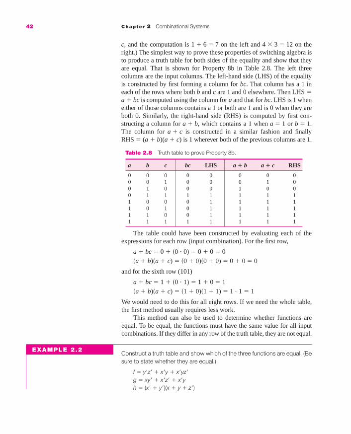
42 Chapter 2 Combinational Systems
The table could have been constructed by evaluating each of the expressions for each row (input combination). For the first row,
a � bc � 0 � �0 � 0) � 0 � 0 � 0
�a � b)�a � c) � �0 � 0)�0 � 0) � 0 � 0 � 0
and for the sixth row (101)
a � bc � 1 � �0 � 1) � 1 � 0 � 1
�a � b)�a � c) � �1 � 0)�1 � 1) � 1 � 1 � 1
We would need to do this for all eight rows. If we need the whole table,the first method usually requires less work.
This method can also be used to determine whether functions areequal. To be equal, the functions must have the same value for all inputcombinations. If they differ in any row of the truth table, they are not equal.
Construct a truth table and show which of the three functions are equal. (Besure to state whether they are equal.)
f � y�z� � x�y � x�yz�
g � xy� � x�z� � x�yh � (x� � y�)(x � y � z�)
EXAMPLE 2.2
Table 2.8 Truth table to prove Property 8b.
a b c bc LHS a � b a � c RHS
0 0 0 0 0 0 0 00 0 1 0 0 0 1 00 1 0 0 0 1 0 00 1 1 1 1 1 1 11 0 0 0 1 1 1 11 0 1 0 1 1 1 11 1 0 0 1 1 1 11 1 1 1 1 1 1 1
c, and the computation is 1 � 6 � 7 on the left and 4 � 3 � 12 on theright.) The simplest way to prove these properties of switching algebra isto produce a truth table for both sides of the equality and show that theyare equal. That is shown for Property 8b in Table 2.8. The left threecolumns are the input columns. The left-hand side (LHS) of the equalityis constructed by first forming a column for bc. That column has a 1 ineach of the rows where both b and c are 1 and 0 elsewhere. Then LHS �a � bc is computed using the column for a and that for bc. LHS is 1 wheneither of those columns contains a 1 or both are 1 and is 0 when they areboth 0. Similarly, the right-hand side (RHS) is computed by first con-structing a column for a � b, which contains a 1 when a � 1 or b � 1.The column for a � c is constructed in a similar fashion and finallyRHS � (a � b)(a � c) is 1 wherever both of the previous columns are 1.
mar91647_c02_029_110.qxd 10/22/08 12:56 PM Page 42

2.2 Switching Algebra 43
The truth table was constructed for each of the three functions (using thesame technique as we did in developing Table 2.8). For input combination 1 0 1, f � 0, but g � h � 1. Thus, f is not equal to either of the other func-tions. The columns for g and h are identical; thus, g � h.
2.2.3 Manipulation of Algebraic Functions
Before adding some properties that are useful in simplifying algebraicexpressions, it is helpful to introduce some terminology that will makethe discussion simpler.
A literal is the appearance of a variable or its complement. Examplesare a and b�. In determining the complexity of an expression, one of themeasures is the number of literals. Each appearance of a variable iscounted. Thus, for example, the expression
ab� � bc�d � a�d � e�
contains eight literals.A product term is one or more literals connected by AND operators.
In the previous example, there are four product terms, ab�, bc�d, a�d, ande�. Notice that a single literal is a product term.
A standard product term, also called a minterm, is a product termthat includes each variable of the problem, either uncomplemented orcomplemented. Thus, for a function of four variables, w, x, y, and z, theterms w�xyz� and wxyz are standard product terms, but wy�z is not.
A sum of products expression (often abbreviated SOP) is one ormore product terms connected by OR operators. The previous expressionmeets this definition as do each of the following:
w�xyz� � wx�y�z� � wx�yz � wxyz (4 product terms)
x � w�y � wxy�z (3 product terms)
x� � y � z (3 product terms)
wy� (1 product term)
z (1 product term)
It is usually possible to write several different SOP expressions for thesame function.
x y z y�z� x�y x�yz� f xy� x�z� x�y g x�� y� x � y � z� h
0 0 0 1 0 0 1 0 1 0 1 1 1 10 0 1 0 0 0 0 0 0 0 0 1 0 00 1 0 0 1 1 1 0 1 1 1 1 1 10 1 1 0 1 0 1 0 0 1 1 1 1 11 0 0 1 0 0 1 1 0 0 1 1 1 11 0 1 0 0 0 0 1 0 0 1 1 1 11 1 0 0 0 0 0 0 0 0 0 0 1 01 1 1 0 0 0 0 0 0 0 0 0 1 0
[SP 4, 5; EX 4, 5]
mar91647_c02_029_110.qxd 10/22/08 12:56 PM Page 43

44 Chapter 2 Combinational Systems
A canonical sum, or sum of standard product terms, is just a sum ofproducts expression where all of the terms are standard product terms.The first example is the only canonical sum (if there are four variables inall of the problems). Often, the starting point for algebraic manipulationsis with canonical sums.
A minimum sum of products expression is one of those SOP expres-sions for a function that has the fewest number of product terms. If thereis more than one expression with the fewest number of terms, then min-imum is defined as one or more of those expressions with the fewestnumber of literals. As implied by this wording, there may be more thanone minimum solution to a given problem. Each of the following expres-sions are equal (meaning that whatever values are chosen for x, y, and z,each expression produces the same value). Note that the first is a sum ofstandard product terms.
(1) x�yz� � x�yz � xy�z� � xy�z � xyz 5 terms, 15 literals
(2) x�y � xy� � xyz 3 terms, 7 literals
(3) x�y � xy� � xz 3 terms, 6 literals
(4) x�y � xy� � yz 3 terms, 6 literals
Expressions (3) and (4) are the minima. (It should be clear that those areminimum among the expressions shown; it is not so obvious that thereis not yet another expression with fewer terms or literals.) (A word ofcaution: When looking for all of the minimum solutions, do not includeany solution with more terms or more literals than the best alreadyfound.)
Actually, we have enough algebra at this point to be able to go fromthe first expression to the last two. First, we will reduce the first expres-sion to the second:
x�yz� � x�yz � xy�z� � xy�z � xyz
� (x�yz� � x�yz) � (xy�z� � xy�z) � xyz associative
� x�y(z� � z) � xy�(z� � z) � xyz distributive
� x�y � 1 � xy� � 1 � xyz complement
� x�y � xy� � xyz identity
The first step takes advantage of P2a, which allows us to group terms inany way we wish. We then utilized P8a to factor x�y out of the first twoterms and xy� out of the third and fourth terms. Next we used P5aa toreplace z� � z by 1. In the final step, we used P3b to reduce the expression.
The last three steps can be combined into a single step. We can adda property
P9a. ab � ab� � a P9b. (a � b)(a � b�) � a
where, in the first case, a � x�y and b � z�. Thus, if there are two prod-uct terms in a sum that are identical, except that one of the variables is
adjacency
mar91647_c02_029_110.qxd 10/22/08 12:56 PM Page 44

2.2 Switching Algebra 45
uncomplemented in one and complemented in the other, they can becombined, using P9a. (The proof of this property follows the same threesteps we used before—P8a to factor out the a, P5a to replace b � b� by1, and finally P3b to produce the result.) The dual can be proved usingthe dual steps, P8b, P5b, and P3a.
The easiest way to get to expression (3), that is, to go to six literals,is to use P6a, and make two copies of xy�z, that is,
xy�z � xy�z � xy�z
The expression becomes
x�yz� � x�yz � xy�z� � xy�z � xyz � xy�z
� �x�yz� � x�yz) � �xy�z� � xy�z) � �xyz � xy�z)
� x�y�z� � z) � xy��z� � z) � xz�y � y�)
� x�y � 1 � xy� � 1 � xz � 1� x�y � xy� � xz
We added the second copy of xy�z at the end and combined it with the lastterm (xyz). The manipulation then proceeded in the same way as before.The other expression can be obtained in a similar manner by using P6aon x�yz and combining the second copy with xyz. Notice that we freelyreordered the terms in the first sum of products expression when weutilized P6a to insert a second copy of one of the terms.
In general, we may be able to combine a term on the list with morethan one other term. If that is the case, we can replicate a term as manytimes as are needed.
Another property that will allow us to reduce the system to six liter-als without the need to make extra copies of a term is
P10a. a � a�b � a � b P10b. a(a� � b) � ab
We can demonstrate the validity of P10a by using P8b, P5a, and P3bb asfollows:
a � a�b � �a � a�) �a � b) distributive
� 1 � �a � b) complement
� a � b identity
P10b can be demonstrated as follows:
a�a� � b) � aa� � ab � 0 � ab � ab
We can apply this property to the example by factoring x out of the lasttwo terms:
x�y � xy� � xyz
� x�y � x�y� � yz) distributive
� x�y � x�y� � z) simplification
� x�y � xy� � xz distributive
simplification
mar91647_c02_029_110.qxd 10/22/08 12:56 PM Page 45

46 Chapter 2 Combinational Systems
We used P10a where a � y� and b � z in going from line 2 to 3. Instead,we could have factored y out of the first and last terms, producing
y(x� � xz) � xy�
� y(x� � z) � xy�
� x�y � yz � xy�
which is the other six literal equivalent.Consider the following example, an expression in canonical form.
a�b�c� � a�bc� � a�bc � ab�c�
The first two terms can be combined using P9a, producing
a�c� � a�bc � ab�c�
Now, we can factor a� from the first two terms and use P10a to reduce this to
a�c� � a�b � ab�c�
and repeat the process with c� and the first and last terms, resulting in theexpression
a�c� � a�b � b�c�
Although this expression is simpler than any of the previous ones, it is notminimum. With the properties we have developed so far, we have reacheda dead end, and we have no way of knowing that this is not the minimum.Returning to the original expression, we can group the first term with the lastand the middle two terms. Then, when we apply P9a, we get an expressionwith only two terms and four literals:
a�b�c� � a�bc� � a�bc � ab�c�
� b�c� � a�b
Later, we will see a property that allows us to go from the three-termexpression to the one with only two terms.
Each terminology defined earlier has a dual that will also prove useful.A sum term is one or more literals connected by OR operators.
Examples are a � b� � c and b� (just one literal).A standard sum term, also called a maxterm, is a sum term that
includes each variable of the problem, either uncomplemented orcomplemented. Thus, for a function of four variables, w, x, y, and z, theterms w� � x � y � z� and w � x � y � z are standard sum terms, butw � y� � z is not.
A product of sums expression (POS) is one or more sum terms con-nected by AND operators. Examples of product of sums expressions:
�w � x)�w � y) 2 terms
w�x � y) 2 terms
w 1 term
EXAMPLE 2.3
mar91647_c02_029_110.qxd 10/22/08 12:56 PM Page 46

2.2 Switching Algebra 47
w � x 1 term
�w � x� � y� � z�)�w� � x � y � z�) 2 terms
A canonical product, or product of standard sum terms, is just aPOS expression in which all of the terms are standard sum terms. Thelast example above is the only canonical sum (if there are four variablesin all of the problems). Often, the starting point for algebraic manipula-tions is with canonical sums.
Minimum is defined the same way for both POS and SOP, namely,the expressions with the fewest number of terms, and, among those withthe same number of terms, those with the fewest number of literals. Agiven function (or expression) can be reduced to minimum sum of prod-ucts form and to minimum product of sums form. They may both havethe same number of terms and literals or either may have fewer than theother. (We will see examples later, when we have further developed ourminimization techniques.)
An expression may be in sum of products form, product of sumsform, both, or neither. Examples are
SOP: x�y � xy� � xyz
POS: �x � y�)�x� � y)�x� � z�)
both: x� � y � z or xyz�
neither: x�w� � yz) or z� � wx�y � v�xz � w�)
We will now look at an example of the simplification of functions inmaxterms form. (Later, we will look at methods of going from sum ofproducts to product of sums and from product of sums to sum of prod-ucts forms.)
g � (w� � x� � y � z�)(w� � x� � y � z)(w � x� � y � z�)
The first two terms can be combined, using P9b, where
a � w� � x� � y and b � z�
producing
g � (w� � x� � y)(w � x� � y � z�)
That can most easily be reduced further by using P6b, to create a secondcopy of the first term, which can be combined with the last term, where
a � x� � y � z� and b � w
producing the final answer
g � (w� � x� � y)(x� � y � z�)
We could also do the following manipulation (parallel to what we didwith the SOP expression)
mar91647_c02_029_110.qxd 10/22/08 12:56 PM Page 47

48 Chapter 2 Combinational Systems
Figure 2.7 Block diagram of f in sumof standard products form.
xy�z�
f
x�yz
x�yz�
xy�z
xyz
This is an example of a two-level circuit. The number of levels is themaximum number of gates through which a signal must pass from the
[SP 6, 7, 8, 9; EX 6, 7, 8, 9]
g � (w� � x� � y)(w � x� � y � z�)
� x� � y � w�(w � z�) [P8b]� x� � y � w�z� [P10b]� (x� � y � w�)(x� � y � z�) [P8b]
which, after reordering the literals in the first set of parentheses, is thesame expression as before.
2.3 IMPLEMENTATION OF FUNCTIONSWITH AND, OR, AND NOT GATES
We will first look at the implementation of switching functions using net-works of AND, OR, and NOT gates. (After all, the goal of our design isto produce the block diagram of a circuit to implement the given switchingfunction.) When we defined minimum SOP expressions, we introduced,as an example, the function
f � x�yz� � x�yz � xy�z� � xy�z � xyz
A block diagram of a circuit to implement this is shown in Figure 2.7.Each of the product terms is formed by an AND gate. In this example,all of the AND gates have three inputs. The outputs of the AND gatesare used as inputs to an OR (in this case a five-input OR). This imple-mentation assumes that all of the inputs are available, both uncomple-mented and complemented (that is, for example, both x and x� areavailable as inputs). This is usually the case if the input to the combina-tional logic circuit comes from a flip flop, a storage device in sequentialsystems. It is not usually true, however, if the input is a system input.
mar91647_c02_029_110.qxd 10/22/08 12:56 PM Page 48

2.3 Implementation of Functions with AND, OR, and NOT Gates 49
input to the output. In this example, all signals go first through an ANDgate and then through an OR. When inputs are available both uncomple-mented and complemented, implementations of both SOP and POSexpressions result in two-level circuits.
We saw that this same function can be manipulated to a minimumSOP expression, one version of which is
f � x�y � xy� � xz
This, of course, leads to a less complex circuit, namely, the one shown inFigure 2.8.
We have reduced the complexity of the circuit from six gates with 20gate inputs (three to each of the five ANDs and five to the OR) to onewith four gates and 9 gate inputs. The simplest definition of minimum fora gate network is minimum number of gates and, among those with thesame number of gates, minimum number of gate inputs. For two-levelcircuits, this always corresponds to minimum sum of products or mini-mum product of sums functions.
If complemented inputs are not available, then an inverter (a NOTgate) is needed for each input that is required to be complemented(x and y in this example). The circuit of Figure 2.9 shows the NOT gatesthat must be added to the circuit of Figure 2.8 to implement f. Note thatin this version we showed each input once, with that input line con-nected to whatever gates required it. That is surely what happens whenwe actually construct the circuit. However, for clarity, we will draw cir-cuits more like the previous one (except, of course, we will only haveone NOT gate for each input, with the output of that gate going to thosegates that require it). (This is a three-level circuit because some of thepaths pass through three gates: a NOT, an AND, and then an OR.)
Figure 2.8 Minimum sumof productimplementation of f.
x
y�f
x�
y
x
z
Figure 2.9 Circuit with onlyuncomplemented inputs.
x
z
f
y
A POS expression (assuming all inputs are available both uncom-plemented and complemented) corresponds to a two-level OR–ANDnetwork. For this same example, the minimum POS (although that is notobvious based on the algebra we have developed to this point)
f � (x � y)(x� � y� � z)
is implemented with the circuit of Figure 2.10.
Figure 2.10 A product of sumsimplementation.
x
y
x�
zy�
f
mar91647_c02_029_110.qxd 10/22/08 12:56 PM Page 49

50 Chapter 2 Combinational Systems
This is a four-level circuit because the signals x and z pass firstthrough an AND gate, then an OR, then an AND, and finally through anOR—a total of four gates.
If we take the version of f used for Figure 2.8, and factor x from the last twoterms, we obtain
f � x�y � x(y� � z)
That would result in the three-level circuit
EXAMPLE 2.4
Figure 2.11 A multilevel circuit.
hwx�
w�
z
x
v
y
z�
fx
z
y
x�
y �
This (three-level) solution uses 4 two-input gates.
Gates are typically available in dual in-line pin packages (DIPs) of14 connector pins. These packages are often referred to as chips. (Largerpackages of 16, 18, 22, and more pins are used for more complex logic.)These packages contain integrated circuits (ICs). Integrated circuits are
When we implement functions that are in neither SOP nor POSform, the resulting circuits are more than two levels. As an example, con-sider the following function:
h � z� � wx�y � v(xz � w�)
We begin inside the parentheses and build an AND gate with inputs x andz. The output of that goes to an OR gate, the other input of which is w�.That is ANDed with v, which is ORed with the input z� and the output ofthe AND gate, producing wx�y, which results in the circuit of Figure 2.11.
mar91647_c02_029_110.qxd 10/22/08 4:56 PM Page 50
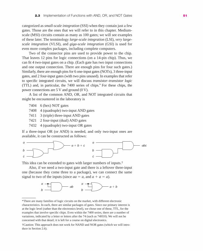
2.3 Implementation of Functions with AND, OR, and NOT Gates 51
categorized as small-scale integration (SSI) when they contain just a fewgates. Those are the ones that we will refer to in this chapter. Medium-scale (MSI) circuits contain as many as 100 gates; we will see examplesof these later. The terminology large-scale integration (LSI), very large-scale integration (VLSI), and giga-scale integration (GSI) is used foreven more complex packages, including complete computers.
Two of the connector pins are used to provide power to the chip.That leaves 12 pins for logic connections (on a 14-pin chip). Thus, wecan fit 4 two-input gates on a chip. (Each gate has two input connectionsand one output connection. There are enough pins for four such gates.)Similarly, there are enough pins for 6 one-input gates (NOTs), 3 three-inputgates, and 2 four-input gates (with two pins unused). In examples that referto specific integrated circuits, we will discuss transistor–transistor logic(TTL) and, in particular, the 7400 series of chips.* For these chips, thepower connections are 5 V and ground (0 V).
A list of the common AND, OR, and NOT integrated circuits thatmight be encountered in the laboratory is
7404 6 (hex) NOT gates7408 4 (quadruple) two-input AND gates7411 3 (triple) three-input AND gates7421 2 four-input (dual) AND gates7432 4 (quadruple) two-input OR gates
If a three-input OR (or AND) is needed, and only two-input ones areavailable, it can be constructed as follows:
a � b � ca
c
b
abca
c
b
aba
ba � b
a
b
This idea can be extended to gates with larger numbers of inputs.†
Also, if we need a two-input gate and there is a leftover three-inputone (because they come three to a package), we can connect the samesignal to two of the inputs (since aa � a, and a � a � a).
*There are many families of logic circuits on the market, with different electroniccharacteristics. In each, there are similar packages of gates. Since our primary interest isat the logic level (rather than the electronics level), we chose one of these, TTL, for theexamples that involve specific chips. Even within the 7400 series, there are a number ofvariations, indicated by a letter or letters after the 74 (such as 74H10). We will not beconcerned with that detail; it is left for a course on digital electronics.
†Caution: This approach does not work for NAND and NOR gates (which we will intro-duce in Section 2.6).
mar91647_c02_029_110.qxd 10/22/08 12:56 PM Page 51

52 Chapter 2 Combinational Systems
In the laboratory, logic 0 and logic 1 are represented by two voltages:often 0 and 5 V. Most commonly, the higher voltage is used to represent 1and the lower voltage to represent 0. This is referred to as positive logic.The opposite choice is also possible, that is, use the higher voltage to rep-resent 0. That is referred to as negative logic. When dealing with 1’s and0’s, the concept does not really come up. However, the same electroniccircuit has different logic meanings depending on which choice we make.
Consider the truth table of Table 2.9a, where the behavior of the gateis described just in terms of high (H) and low (L). The positive logicinterpretation of Table 2.9b produces the truth table for an OR gate. Thenegative logic interpretation of Table 2.9c is that of an AND gate.
Most implementations use positive logic; we will do that consis-tently throughout this book. Occasionally, negative logic, or even a mix-ture of the two, is used.
2.4 THE COMPLEMENT
Before we go further, we need to develop one more property. This prop-erty is the only one for which a person’s name is commonly attached—DeMorgan’s theorem.
P11a. (a � b)� � a�b� P11b. (ab)� � a� � b�
The simplest proof of this property utilizes the truth table of Table 2.10.In Table 2.10, we have produced a column for each of the expressions inthe property. (The entries in the table should be obvious because they justinvolve the AND, OR, and NOT operations on other columns.) Note thatthe columns (labeled 11a) for (a � b)� and a�b� are the same and those(labeled 11b) for (ab)� and a� � b�are the same.
DeMorgan
[SP 10, 11; EX 10, 11; LAB*]
Table 2.9
a. High/Low b. Positive logic c. Negative logic
a b f a b f a b f
L L L 0 0 0 1 1 1L H H 0 1 1 1 0 0H L H 1 0 1 0 1 0H H H 1 1 1 0 0 0
*LAB refers to experiments in Appendix D.
1 • ab � ab a1
b0 � a � b � a � ba
0
b
Also, we could connect a logic 1 (�5 V) to one of the inputs of an ANDor a logic 0 (ground) to one of the inputs of an OR:
mar91647_c02_029_110.qxd 10/22/08 12:56 PM Page 52

2.4 The Complement 53
The property can be extended to more than two operands easily.
P11aa. (a � b � c . . .)� � a�b�c� . . .P11bb. (abc . . .)� � a� � b� � c� . . .
For P11aa, with three variables, the proof goes
(a � b � c)� � [(a � b) � c]� � (a � b)�c� � a�b�c�
Just look at the (ab)� and a�b� columns of the truth table and compare theexpressions for a � 0 and b � 1 (or for a � 1 and b � 0):
(0 � 1)� � 0� � 1 0� � 1� � 1 � 0 � 0
There will be times when we are given a function and need to find itscomplement, that is, given f(w, x, y, z), we need f �(w, x, y, z). The straight-forward approach is to use DeMorgan’s theorem repeatedly.
f � wx�y � xy� � wxz
then
f � � (wx�y � xy� � wxz)�
� (wx�y)�(xy�)�(wxz)� [P11a]
� (w� � x � y�)(x� � y)(w� � x� � z�) [P11b]
Note that if the function is in SOP form, the complement is in POS form(and the complement of a POS expression is an SOP one).
To find the complement of more general expressions, we can repeat-edly apply DeMorgan’s theorem or we can follow this set of rules:
1. Complement each variable (that is, a to a� or a� to a).
2. Replace 0 by 1 and 1 by 0.
3. Replace AND by OR and OR by AND, being sure to preserve theorder of operations. That sometimes requires additional parentheses.
COMMON MISTAKE: The NOT does not distribute through theparentheses. Thus,
(ab)� a�b� and (a + b)� a� + b�
and, for example,
ab + a�b� 1
EXAMPLE 2.5
Table 2.10 Proof of DeMorgan’s theorem.
a b a � b (a � b)� a� b� a�b� ab (ab)� a� � b�
0 0 0 1 1 1 1 0 1 10 1 1 0 1 0 0 0 1 11 0 1 0 0 1 0 0 1 11 1 1 0 0 0 0 1 0 0
11a 11a 11b 11b
mar91647_c02_029_110.qxd 10/22/08 12:56 PM Page 53

54 Chapter 2 Combinational Systems
EXAMPLE 2.6
Table 2.11 A two-variabletruth table.
a b f
0 0 00 1 11 0 11 1 1
[SP 12; EX 12]
f � ab�(c � d�e) � a�bc�
f� � [a� � b � c�(d � e�)][a � b� � c]
Note that in f, the last operation to be performed is an OR of the complexfirst term with the product term. To preserve the order, parentheseswere needed in f�; making the AND the last operation.
We would produce the same result, with much more work, by usingP11a and P11b over and over again:
f� � [ab�(c � d�e) � a�bc�]�
� [ab�(c � d�e)]�[a�bc�]�
� [a� � b � (c � d�e)�][a � b� � c]
� [a� � b � c�(d�e)�][a � b� � c]
� [a� � b � c�(d � e�)][a � b� � c]
2.5 FROM THE TRUTH TABLE TOALGEBRAIC EXPRESSIONS
Often, a design problem is stated in terms of the truth table that describesthe output in terms of the inputs. Other times, verbal descriptions of sys-tems can most easily be translated into the truth table. Thus, we need theability to go from the truth table to an algebraic expression. To under-stand the process, consider the two-variable truth table of Table 2.11.
Because this is a two-variable problem, the truth table has 4(� 22)rows, that is, there are 4 possible combinations of inputs. (This is thetruth table for the OR as we defined it at the beginning of this chapter, butthat is irrelevant to this discussion.) What the table says is that
f is 1 if a � 0 AND b � 1 OR
if a � 1 AND b � 0 OR
if a � 1 AND b � 1
However, this is the same as saying
f is 1 if a� � 1 AND b � 1 OR
if a � 1 AND b� � 1 OR
if a � 1 AND b � 1
But a� � 1 AND b � 1 is the same as saying a�b � 1 and thus
f is 1 if a�b � 1 OR if ab� � 1 OR if ab � 1
That finally produces the expression
f � a�b � ab� � ab
mar91647_c02_029_110.qxd 10/22/08 12:56 PM Page 54

2.5 From the Truth Table to Algebraic Expressions 55
Each row of the truth table corresponds to a product term. An SOPexpression is formed by ORing those product terms corresponding torows of the truth table for which the function is 1. Each product term haseach variable included, with that variable complemented when the entryin the input column for that variable contains a 0 and uncomplementedwhen it contains a 1. Thus, for example, row 10 produces the term ab�.These product terms include all of the variables; they are minterms.Minterms are often referred to by number, by just converting the binarynumber in the input row of the truth table to decimal. Both of the fol-lowing notations are common:
f�a, b� � m1 � m2 � m3
f�a, b� � �m�1, 2, 3�
Note: If we use minterm numbers, we must include the variable namesin the function name, such as f (a, b). If we write an algebraic expres-sion, such as f = a�b + ab� + ab, we can use just f, since the variables areobvious.
We show, in Table 2.12, the minterms and minterm numbers that areused for all functions of the three variables A, B, and C.
For a specific function, those terms for which the function is 1 areused to form an SOP expression for f, and those terms for which the func-tion is 0 are used to form an SOP expression for f �. We can then comple-ment f� to form a POS expression for f.
Table 2.12 Minterms.
ABC Minterm Number
0 0 0 A�B�C� 00 0 1 A�B�C 10 1 0 A�BC� 20 1 1 A�BC 31 0 0 AB�C� 41 0 1 AB�C 51 1 0 ABC� 61 1 1 ABC 7
ABC f f�
0 0 0 0 10 0 1 1 00 1 0 1 00 1 1 1 01 0 0 1 01 0 1 1 01 1 0 0 11 1 1 0 1
where the truth table shows both the function, f, and its complement, f�. Wecan write
f(A, B, C) � �m(1, 2, 3, 4, 5)
� A�B�C � A�BC� � A�BC � AB�C� � AB�C
Either from the truth table, or by recognizing that every minterm is includedin either f or f�, we can then write
f�(A, B, C) � �m(0, 6, 7)
� A�B�C� � ABC� � ABC
EXAMPLE 2.7
mar91647_c02_029_110.qxd 10/22/08 12:56 PM Page 55

56 Chapter 2 Combinational Systems
We can then complement f� to get a sum of maxterms.*
f � (f�)� � (A � B � C)(A� � B� � C)(A� � B� � C�)
The two sum of minterm forms are SOP expressions. In most cases,including this one, the sum of minterms expression is not a minimum sumof products expression. We could reduce f from 5 terms with 15 literals toeither of two functions with 3 terms and 6 literals as follows:
f � A�B�C � A�BC� � A�BC � AB�C� � AB�C
� A�B�C � A�B � AB� [P9a, P9a]
� A�C � A�B � AB�
� B�C � A�B � AB�
where the final expressions are obtained using P8a and P10a on the firstterm and either the second or the third. Similarly, we can reduce f� from 3 terms with 9 literals to 2 terms with 5 literals, using P9a:
f� � A�B�C� � AB
Using P11, we can then obtain the minimum POS expression for f.
f = (A + B + C)(A� + B�)
To find a minimum POS expression, we can either manipulate the previousPOS expression (using P9b on the last two terms) or simplify the SOPexpression for f� and then use DeMorgan to convert it to a POS expression.Both approaches produce the same result.
In much of the material of Chapter 3, we will specify functions byjust listing their minterms (by number). We must, of course, list the vari-ables of the problem as part of that statement. Thus,
f(w, x, y, z) � �m(0, 1, 5, 9, 11, 15)
is the simplest way to specify the function
f � w�x�y�z� � w�x�y�z � w�xy�z � wx�y�z � wx�yz � wxyz
If the function includes don’t cares, then those terms are included ina separate sum (�).
*It is possible to obtain POS expressions directly from the truth table without first findingthe SOP expression. Each 0 of f produces a maxterm in the POS expression. We haveomitted that approach here, because it tends to lead to confusion.
mar91647_c02_029_110.qxd 10/22/08 12:56 PM Page 56

2.5 From the Truth Table to Algebraic Expressions 57
f(a, b, c) � �m(1, 2, 5) � �d(0, 3)
implies that minterms 1, 2, and 5 are included in the function and that 0 and3 are don’t cares, that is the truth table is as follows:
abc f
0 0 0 X0 0 1 10 1 0 10 1 1 X1 0 0 01 0 1 11 1 0 01 1 1 0
EXAMPLE 2.8
Let us now return to the first three of our continuing examples anddevelop algebraic expressions for them.
Using Z2 for CE1, we get
Z2 � A�BCD � AB�CD � ABC�D � ABCD� � ABCD
directly from the truth table. The last term (ABCD) can be combined witheach of the others (using P10a). Thus, if we make four copies of it (usingP6a repeatedly) and then utilize P10a four times, we obtain
Z2 � BCD � ACD � ABD � ABC
No further simplification is possible; this is the minimum sum of productsexpression. Notice that if we used Z1, we would have
Z1 � A�BCD � AB�CD � ABC�D � ABCD�
No simplification is possible. This expression also has four terms, but it has16 literals, whereas the expression for Z2 only has 12.
For CE2, we have either
f � ab�c � abc� or f � ab�c� � abc
depending on which truth table we choose. Again, no simplification ispossible.
For f�, we have (for the first version)
f� � a�b�c� � a�b�c � a�bc� � a�bc � ab�c� � abc� a�b� � a�b � ab�c� � abc [P9a, P9b]� a� � ab�c� � abc � a� � b�c� � bc [P9a, P10a]
Thus, the product of maxterms is
f � (a � b � c) (a � b � c�) (a � b� � c) (a � b� � c�)(a� � b � c) (a� � b� � c�)
and the minimum POS is
f � a (b � c) (b� � c�)
EXAMPLE 2.9
EXAMPLE 2.10
mar91647_c02_029_110.qxd 10/22/08 12:56 PM Page 57
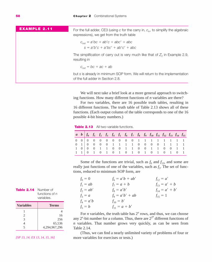
58 Chapter 2 Combinational Systems
For the full adder, CE3 (using c for the carry in, cin, to simplify the algebraicexpressions), we get from the truth table
cout � a�bc � ab�c � abc� � abc
s � a�b�c � a�bc� � ab�c� � abc
The simplification of carry out is very much like that of Z2 in Example 2.9,resulting in
cout � bc � ac � ab
but s is already in minimum SOP form. We will return to the implementationof the full adder in Section 2.8.
We will next take a brief look at a more general approach to switch-ing functions. How many different functions of n variables are there?
For two variables, there are 16 possible truth tables, resulting in 16 different functions. The truth table of Table 2.13 shows all of thesefunctions. (Each output column of the table corresponds to one of the 16possible 4-bit binary numbers.)
EXAMPLE 2.11
Table 2.14 Number offunctions of nvariables.
Variables Terms
1 42 163 2564 65,5365 4,294,967,296
[SP 13, 14; EX 13, 14, 15, 16]
Table 2.13 All two-variable functions.
a b f0 f1 f2 f3 f4 f5 f6 f7 f8 f9 f10 f11 f12 f13 f14 f15
0 0 0 0 0 0 0 0 0 0 1 1 1 1 1 1 1 10 1 0 0 0 0 1 1 1 1 0 0 0 0 1 1 1 11 0 0 0 1 1 0 0 1 1 0 0 1 1 0 0 1 11 1 0 1 0 1 0 1 0 1 0 1 0 1 0 1 0 1
Some of the functions are trivial, such as f0 and f15, and some arereally just functions of one of the variables, such as f3. The set of func-tions, reduced to minimum SOP form, are
f0 � 0 f6 � a�b � ab� f12 � a�
f1 � ab f7 � a � b f13 � a� � b
f2 � ab� f8 � a�b� f14 � a� � b�
f3 � a f9 � a�b� � ab f15 � 1
f4 � a�b f10 � b�
f5 � b f11 � a � b�
For n variables, the truth table has 2n rows, and thus, we can chooseany 2n-bit number for a column. Thus, there are 22n
different functions ofn variables. That number grows very quickly, as can be seen fromTable 2.14.
(Thus, we can find a nearly unlimited variety of problems of four ormore variables for exercises or tests.)
mar91647_c02_029_110.qxd 10/22/08 12:56 PM Page 58

2.6 NAND, NOR, and Exclusive-OR Gates 59
Figure 2.12 NAND gates.
(ab)�a
b(wxyz)�
wx
zy
Figure 2.13 Alternative symbolfor NAND.
a
ba� � b� � (ab)�
Figure 2.14 Symbols for NOR gate.
a
b(a � b)�
a
ba�b�
Why use NAND and NOR gates, rather than AND, OR, and NOTgates? After all, the logic expressions are in terms of AND, OR, and NOToperators and thus the implementation with those gates is straightforward.Many electronic implementations naturally invert (complement) signals;thus, the NAND is more convenient to implement than the AND. Themost important reason is that with either NAND or NOR, only one typeof gate is required. On the other hand, both AND and OR gates arerequired; and, often, NOT gates are needed, as well. As can be seen fromthe circuits of Figure 2.15, NOT gates and two-input AND and OR gatescan be replaced by just two-input NANDs. Thus, these operators are saidto be functionally complete. (We could implement gates with more thantwo inputs using NANDs with more inputs. We could also implementAND, OR, and NOT gates using only NORs; that is left as an exercise.)
Using these gate equivalences, the function, f � x�y � xy� � xz, thatwe first implemented with AND and OR gates in Figure 2.8 (Section 2.3)can now be implemented with NAND gates, as shown in Figure 2.16.
The NAND has the symbol shown in Figure 2.12. Like the AND andthe OR, the NAND is commercially available in several sizes, typicallytwo-, three-, four-, and eight-input varieties. When first introduced, itwas referred to as an AND-NOT, which perfectly describes its function,but the shorter name, NAND, has become widely accepted. Note thatDeMorgan’s theorem states that
(ab)� � a� � b�
and thus an alternative symbol for the two-input NAND is shown inFigure 2.13. The symbols may be used interchangeably; they refer to thesame component.
The NOR gate (OR-NOT) uses the symbols shown in Figure 2.14. Ofcourse, (a � b)� � a�b�. NOR gates, too, are available with more inputs.
2.6 NAND, NOR, ANDEXCLUSIVE-OR GATES
In this section we will introduce three other commonly used types ofgates, the NAND, the NOR, and the Exclusive-OR, and see how toimplement circuits using them.
mar91647_c02_029_110.qxd 10/22/08 12:56 PM Page 59

60 Chapter 2 Combinational Systems
But note that we have two NOT gates in a row in each of the brown paths.They serve no purpose logically (P7 states (a�)� � a), and thus they canbe removed from the circuit, yielding that of Figure 2.17. That is, all ofthe AND and OR gates of the original circuit became NANDs. Nothingelse was changed.
This process can be greatly simplified when we have a circuit con-sisting of AND and OR gates such that
1. the output of the circuit comes from an OR,
2. the inputs to all OR gates come either from a system input or fromthe output of an AND, and
3. the inputs to all AND gates come either from a system input orfrom the output of an OR.
All gates are replaced by NAND gates, and any input coming directlyinto an OR is complemented.
We can obtain the same result by starting at the output gate and put-ting a bubble (a NOT) at both ends of each input line to that OR gate. Ifthe circuit is not two-level, we repeat this process at the input of eachof the OR gates. Thus, the AND/OR implementation of f becomes that ofFigure 2.18, where all of the gates have become NAND gates (in one ofthe two notations we introduced earlier).
This approach works with any circuit that meets these conditions,with only one additional step. If an input comes directly into an OR gate,
Figure 2.15 Functional completeness of NAND.
a (aa)� � a �
NOT
OR
b
aab
(ab)�
AND
b
a
a � b � a � b
Figure 2.16 NAND gate implementation.
x �
y
fx
y �
x
z
Figure 2.17 Better NAND gateimplementation.
x�
xf
y�
x
z
y
mar91647_c02_029_110.qxd 10/22/08 12:56 PM Page 60

2.6 NAND, NOR, and Exclusive-OR Gates 61
there is no place for the second NOT; thus, that input must be comple-mented. For example, the circuit for h
h � z� � wx�y � v(xz � w�)
is shown in Figure 2.19. Again, all of the AND and OR gates becomeNANDs, but the two inputs that came directly into the OR gates werecomplemented.
Figure 2.18 Double NOT gateapproach.
x �
y
x
y �
x
z
f
Figure 2.19 A multilevel NAND implementation.
v
z
x
w
yx� h
w �w
z �z
f � wx(y � z) � x�y
This would be implemented with AND and OR gates in either of two ways.
EXAMPLE 2.12
xw
f
x�
y
y
z
f
x�
y
y
z
w
x
The first version can be directly converted to NAND gates, as follows.
xw
f
x �
y
y �
z �
mar91647_c02_029_110.qxd 10/22/08 12:56 PM Page 61

62 Chapter 2 Combinational Systems
The second version cannot be converted to NAND gates without adding anextra NOT gate, because it violates the third rule—an AND gets an inputfrom another AND. Thus, this circuit would become
f
x �
y
y �
z �
w
x
x
y�
x�
y
x�
z�
g
where the NOT is required to implement the AND that forms wx. Expres-sions such as this one are often obtained starting from SOP solutions. Wewill see some examples of this in Section 2.8.
The dual approach works for implementing circuits with NORgates. When we have a circuit consisting of AND and OR gates such that
1. the output of the circuit comes from an AND,
2. the inputs to OR gates come either from a system input or from theoutput of an AND, and
3. the inputs to AND gates come either from a system input or fromthe output of an OR.
Then all gates can be converted to NOR gates, and, if an input comesdirectly into an AND gate, that input must be complemented.
g � (x � y�)(x� � y)(x� � z�)
is implemented
where all gates are NOR gates.
EXAMPLE 2.13
mar91647_c02_029_110.qxd 10/22/08 12:56 PM Page 62

2.6 NAND, NOR, and Exclusive-OR Gates 63
The Exclusive-OR gate implements the expression
a�b � ab�
which is sometimes written a � b. The terminology comes from the def-inition that a � b is 1 if a � 1 (and b � 0) or if b � 1 (and a � 0), butnot both a � 1 and b � 1. The operand we have been referring to as OR(�) is sometimes referred to as the Inclusive-OR to distinguish it fromthe Exclusive-OR. The logic symbol for the Exclusive-OR is similar tothat for the OR except that it has a double line on the input, as shown inFigure 2.20a. Also commonly available is the Exclusive-NOR gate, asshown in Figure 2.20b. It is just an Exclusive-OR with a NOT on the out-put and produces the function
(a � b)� � a�b� � ab.
This sometimes is referred to as a comparator, since the Exclusive-NORis 1 if a � b, and is 0 if a b.
A NAND gate implementation of the Exclusive-OR is shown inFigure 2.21a, where only uncomplemented inputs are assumed.
The two NOT gates (implemented as two-input NANDs) can bereplaced by a single gate, as shown in Figure 2.21b, since
a(a� � b�) � b(a� � b�) � aa� � ab� � ba� � bb� � ab� � a�b
Figure 2.20 (a) An Exclusive-OR gate. (b) AnExclusive-NORgate.
a � ba
b
(a � b)�a
b
(a)
(b)
Figure 2.21 Exclusive-OR gates.
a
b
a
b
(a) (b)
Some useful properties of the Exclusive-OR are
(a � b)� � (a�b � ab�)� � (a � b�)(a� � b) � a�b� � ab
a� � b � (a�)�b � (a�)b� � ab � a�b� � (a � b)�
(a � b�) � (a � b)�
a � 0 � a � (a� � 0 � a � 1)
a � 1 � a� � (a� � 1 � a � 0)
The Exclusive-OR has both the commutative and associative properties,that is,
a � b � b � a
(a � b) � c � a � (b � c)
mar91647_c02_029_110.qxd 10/22/08 12:56 PM Page 63

EXAMPLE 2.14
The number of gates and packages are shown in the left part of the follow-ing table
Gates Packs
Inputs AND OR AND OR NAND Packs
2 3 2 1 5 13 2 1 1 1 3 14 1 1 1 1
Total 6 3 3 1 9 3
With AND and OR gates, four packages are needed: three ANDs and oneOR package (because the 2 two-input OR gates can be constructed withthe leftover three-input gates).
If all of the gates are converted to NANDs (and some of the inputs are com-plemented) the gate and package count is shown in the right part of the table.
64 Chapter 2 Combinational Systems
A list of some of the more common NAND, NOR, and Exclusive-OR integrated circuit packages that we may encounter in the laboratoryis as follows:
7400 4 (quadruple) two-input NAND gates7410 3 (triple) three-input NAND gates7420 2 (dual) four-input NAND gates7430 1 eight-input NAND gate7402 4 (quadruple) two-input NOR gates7427 3 (triple) three-input NOR gates7486 4 (quadruple) two-input Exclusive-OR gates
To build a circuit, we utilize packages. Even if we only need 1 three-input NAND gate, we must buy a package with three gates on it (a 7410).Recognize, however, that a three-input gate can be used as a two-inputgate by connecting two of the inputs together or by connecting one of theinputs to a logic 1.
Consider the following circuit, constructed with ANDs and ORs; the inputvariables have been omitted because they are irrelevant to the discussion.
mar91647_c02_029_110.qxd 10/22/08 12:56 PM Page 64

[SP 15, 16, 17; EX 17, 18, 19; LAB]
2.7 Simplification of Algebraic Expressions 65
absorption
Only three packages are needed. The second four-input gate on the 7420would be used as the fifth two-input gate (by tying three of the inputs together).
2.7 SIMPLIFICATION OF ALGEBRAICEXPRESSIONS*
We have already looked at the process of simplifying algebraic expres-sions, starting with a sum of minterms or a product of maxterms. The pri-mary tools were
P9a. ab � ab� � a P9b. (a � b) (a � b�) � a
P10a. a � a�b � a � b P10b. a(a� � b) � ab
although many of the other properties were used, particularly,
P6a. a � a � a P6b. a � a � a
P8a. a(b � c) � ab � ac P8b. a � bc � (a � b)(a � c)
If the function is stated in other than one of the standard forms, twoother properties are useful. First,
P12a. a � ab � a P12b. a(a � b) � a
The proof of P12a uses P3b, P8a, P4aa, and P3b (again).
a � ab � a � 1 � ab � a(1 � b) � a � 1 � a
Remember that we only need to prove one half of the property, becausethe dual of a property is always true. However, we could have provenP12b using the duals of each of the theorems we used to prove P12a.Instead, we could distribute the a from the left side of P12b, producing
a � a � ab � a � ab
However, that is just the left side of P12a, which we have already provedis equal to a.
P10a and P12a look very similar; yet we used two very differentapproaches to demonstrate their validity. In P10a, we did
a � a�b � (a � a�)(a � b) � 1 � (a � b) � a � b[P8b, P5a, P3bb]
whereas for P12a, we used P3b, P8a, P4aa, and P3b. How did we knownot to start the proof of P11a by using P8b to obtain
a � ab � (a � a)(a � b) � a(a � b)?
Those steps are all valid, but they do not get us anywhere toward show-ing that these expressions equal a. Similarly, if we started the proof ofP10a by using P3b, that is,
a � a�b � a � 1 � a�b
*At this point, some instructors prefer to introduce the Karnaugh map. Section 3.1 couldbe studied next, and the remaining material could be studied along with Appendix A,which shows the relationship between algebraic manipulation and the Karnaugh map.
mar91647_c02_029_110.qxd 10/22/08 12:56 PM Page 65
we also do not get anywhere toward a solution. How does the noviceknow where to begin? Unfortunately, the answer to that is either trial anderror or experience. After solving a number of problems, we can oftenmake the correct guess as to where to start on a new one. If that approachdoes not work, then we must try another one. This is not much of a prob-lem in trying to demonstrate that two expressions are equal. We know thatwe can quit when we have worked one side to be the same as the other.
Before proceeding with a number of examples, some comments onthe process are in order. There is no algorithm for algebraic simplifica-tion, that is, there is no ordered list of properties to apply. On the otherhand, of the properties we have up to this point, 12, 9, and 10 are the onesmost likely to reduce the number of terms or literals. Another difficultyis that we often do not know when we are finished, that is, what is theminimum. In most of the examples we have worked so far, the finalexpressions that we obtained appear to be as simple as we can go. How-ever, we will see a number of examples where it is not obvious that thereis not a more minimum expression. We will not be able to get around thisuntil Chapter 3 when we develop other simplification methods. (Notethat in the Solved Problems and the Exercises, the number of terms andliterals in the minimum solution is given. Once that is reached, we knowwe are done; if we end up with more, we need to try another approach.)
We will now look at several examples of algebraic simplification.
xyz � x�y � x�y�
� xyz � x� [P9a]
� x� � yz [P10a]
where a � x�, a� � x, and b � yz
wx � wxy � w�yz � w�y�z � w�xyz�
� (wx � wxy) � (w�yz � w�y�z) � w�xyz�
� wx � w�z � w�xyz� [P12a, P9a]� wx � w�(z � xyz�)� wx � w�(z � xy) [P10a]� wx � w�z � w�xy� w�z � x(w � w�y)� w�z � x(w � y) [P10a]� w�z � wx � xy
P10a could have been used first with wx and w�xyz�(resulting in xyz�). Thatapproach, however, would leave us with an expression
w�z � wx � xyz�
for which there are no algebraic clues as to how to proceed. The only waywe can now reduce it is to add terms to the expression. Shortly, we willintroduce another property that will enable us to go from this expression tothe minimum one.
66 Chapter 2 Combinational Systems
EXAMPLE 2.15
EXAMPLE 2.16
mar91647_c02_029_110.qxd 10/22/08 12:56 PM Page 66

2.7 Simplification of Algebraic Expressions 67
(x � y)(x � y � z�) � y� � (x � y) � y� [P12b]� x � (y � y�) � x � 1 � 1 [P5a, P4a]
(a � b� � c)(a � c�)(a� � b� � c)(a � c � d)� (b� � c)(a � c�)(a � d) [P9b, P10b]
where the second simplification really took several steps
(a � c�)(a � c � d) � a � c�(c � d) � a � c�d � (a � c�)(a � d)
One more tool is useful in the algebraic simplification of switchingfunctions. The operator consensus (indicated by the symbol ¢) is definedas follows:
For any two product terms where exactly one variable appearsuncomplemented in one and complemented in the other, the consensus isdefined as the product of the remaining literals. If no such variable existsor if more than one such variable exists, then the consensus is undefined.If we write one term as at1 and the second as a�t2 (where t1 and t2 repre-sent product terms), then, if the consensus is defined,
at1 ¢ a�t2 � t1t2
ab�c ¢ a�d � b�cdab�c ¢ a�cd � b�cdabc� ¢ bcd� � abd�
b�c�d� ¢ b�cd� � b�d�
abc� ¢ bc�d � undefined—no such variablea�bd ¢ ab�cd � undefined—two variables, a and b
We then have the following property that is useful in reducing functions.
P13a. at1 � a�t2 � t1t2 � at1 � a�t2
P13b. (a � t1)(a� � t2)(t1 � t2) � (a � t1)(a� � t2)
P13a states that the consensus term is redundant and can be removedfrom an SOP expression. (Of course, this property, like all of the others,can be used in the other direction to add a term. We will see an exampleof that shortly.)
A similar kind of simplification can be obtained in POS expressionsusing the dual (P13b). We will not pursue that further.
First, we will derive this property from the others. Using P12a twice,the right-hand side becomes
COMMON MISTAKE: The consensus theorem allows you toremove the consensus term (t1t2), not the two terms thatformed the consensus (at1 + a�t2). For example
ab + b�c + ac = ab + b�c ac
EXAMPLE 2.17
EXAMPLE 2.18
EXAMPLE 2.19
consensus
mar91647_c02_029_110.qxd 10/22/08 12:56 PM Page 67

EXAMPLE 2.20
EXAMPLE 2.21
68 Chapter 2 Combinational Systems
at1 � a�t2 � (at1 � at1t2) � (a�t2 � a�t1t2) [P12a]� at1 � a�t2 � (at1t2 � a�t1t2)
� at1 � a�t2 � t1t2 [P9a]
It is also useful to look at the truth table for this theorem. From Table2.15, we see that the consensus term, t1t2, is 1 only when one of the otherterms is already 1. Thus, if we OR that term with RHS, it does not changeanything, that is, LHS is the same as RHS.
Table 2.15 Consensus.
a t1 t2 at1 a�t2 RHS t1t2 LHS
0 0 0 0 0 0 0 00 0 1 0 1 1 0 10 1 0 0 0 0 0 00 1 1 0 1 1 1 11 0 0 0 0 0 0 01 0 1 0 0 0 0 01 1 0 1 0 1 0 11 1 1 1 0 1 1 1
In Example 2.3 (Section 2.2.3), we reduced the function as
f � a�b�c� � a�bc� � a�bc � ab�c�
to
f1 � a�c� � a�b � b�c�
by combining the first two terms using P9a, and then applying P10a twice.At that point, we were at a dead end. However, we found by starting overwith a different grouping that we could reduce this to
f2 � b�c� � a�b
Indeed, the term eliminated, a�c�, is the consensus of the other terms; wecould use P13a to go from f1 to f2.
g � bc� � abd � acd
Because Properties 1 through 12 produce no simplification, we now tryconsensus. The only consensus term defined is
bc� ¢ acd � abd
Property 13 now allows us to remove the consensus term. Thus,
g � bc� � acd
mar91647_c02_029_110.qxd 10/22/08 12:56 PM Page 68

2.7 Simplification of Algebraic Expressions 69
EXAMPLE 2.23
Reduce
f = c�d� + ac� + ad + bd� + ab
to three terms with six literals. We can use consensus twice.
c�d� ¢ ad = ac� and ad ¢ bd� = ab
Thus, we can remove ac� and ab, leaving
f = c�d� + ad + bd�
With the following function, there is no way to apply Properties 12,9 and 10:
f � w�y� � w�xz � wxy � wyz�
However, we are told that it can be reduced to three terms and eight lit-erals. Next, we try consensus. An approach that ensures that we try tofind the consensus of all pairs of terms is to start with consensus of thesecond term with the first; then try the third with the second and the first;and so forth. Following this approach (or any other) for this example, theonly consensus that exists is
w�xz ¢ wxy � xyz
When a consensus term was part of the SOP expression, P13a allowed usto remove that term and thus simplify the expression. If the consensusterm is not one of the terms in the SOP expression, the same propertyallows us to add it to the expression. Of course, we don’t add anotherterm automatically because that makes the expression less minimum.However, we should keep track of such a term, and, as a last resort, con-sider adding it to the function. Then, see if that term can be used to formother consensus terms and thus reduce the function. In this example, byadding xyz, f becomes
f � w�y� � w�xz � wxy � wyz� � xyz
Now, however,
xyz ¢ wyz� � wxy and xyz ¢ w�y� � w�xz
Thus, we can remove both wxy and w�xz, leaving
f � w�y� � wyz� � xyz (3 terms, 8 literals)
We will now consider an example making use of consensus, as wellas all of the other properties. The usual approach is to try to utilize prop-erties 12, 9, and then 10. When we get as far as we can with these, wethen turn to consensus.
A�BCD � A�BC�D � B�EF � CDE�G � A�DEF � A�B�EF� A�BD � B�EF � CDE�G � A�DEF [P12a, P9a]
But A�BD ¢ B�EF � A�DEF and this reduces toA�BD � B�EF � CDE�G
EXAMPLE 2.22
mar91647_c02_029_110.qxd 10/22/08 12:56 PM Page 69

70 Chapter 2 Combinational Systems
w�xy � wz � xz � w�y�z � w�xy� � wx�z
� wz � w�x � xz � w�y�z [P12a, P9a]
� wz � w�x � w�y�z since wz ¢ w�x � xz [P13a]
But,
wz � w�y�z � z(w � w�y�) � z(w � y�) [P10a]
� wz � w�x � y�z
2.8 MANIPULATION OF ALGEBRAICFUNCTIONS AND NAND GATEIMPLEMENTATIONS
In addition to the need to minimize algebraic expressions, there is some-times the requirement to put an expression in a certain format, such asSOP, sum of minterms, POS, or product of maxterms. Secondly, to meetdesign constraints, we sometimes must manipulate the algebra. In thissection we will look at some examples and introduce one more property.
If we have an SOP expression and need to expand it to sum ofminterms, we have two options. First, we can create a truth table, and, fromthat, follow the approach of Section 2.5 to produce a sum of minterms. Indeed, this approach will work for an expression in any format. The otherapproach is to use P9a to add variables to a term.
f � bc � ac � ab
� bca � bca� � ac � ab
We can repeat the process on the other two terms, producing
f � bca � bca� � acb � acb� � abc � abc�
� abc � a�bc � abc � ab�c � abc � abc�
� a�bc � ab�c � abc� � abc
where P6a was used to remove the duplicate terms.
If two literals were missing from a term, that term would producefour minterms, using P9a repeatedly.
g � x� � xyz � x�y � x�y� � xyz
� x�yz � x�yz� � x�y�z � x�y�z� � xyz
g(x, y, z) � �m(3, 2, 1, 0, 7) � �m(0, 1, 2, 3, 7)
since minterm numbers are usually written in numeric order.
EXAMPLE 2.25
EXAMPLE 2.26
EXAMPLE 2.24
[SP 18; EX 20, 21, 22]
mar91647_c02_029_110.qxd 10/22/08 12:56 PM Page 70

2.8 Manipulation of Algebraic Functions and NAND Gate Implementations 71
To convert to product of maxterms, P9b can be used. For example,
f � (A � B � C)(A� � B�)
� (A � B � C)(A� � B� � C)(A� � B� � C�)
One other property is useful in manipulating functions from oneform to another.
P14a. ab � a�c � (a � c)(a� � b)
(The dual of this is also true; but it is the same property with the variablesb and c interchanged.) This property can be demonstrated by first apply-ing P8a to the right side three times:
(a � c)(a� � b) � (a � c)a� � (a � c) b � aa� � a�c � ab � bc
However, aa� � 0 and bc � a�c ¢ ab, and thus, using P3aa and P13a, weget
aa� � a�c � ab � bc � a�c � ab
which is equal to the left side of the property.This property is particularly useful in converting POS expressions to
SOP and vice versa. We will also use it to manipulate expressions whenusing NAND gates to implement systems.
In Example 2.7, we found the sum of minterms and the minimumSOP expressions, as well as the product of maxterms and the minimumPOS expression for
f(A, B, C) � �m(1, 2, 3, 4, 5)
In Example 2.28, we will start with the minimum POS, and use Property14 to convert it to a SOP.
f � (A � B � C)(A� � B�) � AB� � A�(B � C) � AB� � A�B � A�C
where the a of P14a is A, the b is B � C, and the c is B�. This, indeed, isone of the SOP solutions we found in Example 2.7 for this problem.Although the utilization of this property does not always produce a minimumSOP expression (as it does in this case), it does produce a simpler expres-sion than we would get just using P8a.
f � AA� � AB� � BA� � BB� � CA� � CB�
� AB� � A�B � A�C � B�C
The term B�C can then be removed because it is the consensus of AB� and A�C.
To go from a POS expression (or a more general expression that isneither SOP nor POS) to an SOP expression, we use primarily the follow-ing three properties:
EXAMPLE 2.27
EXAMPLE 2.28
mar91647_c02_029_110.qxd 10/22/08 4:56 PM Page 71
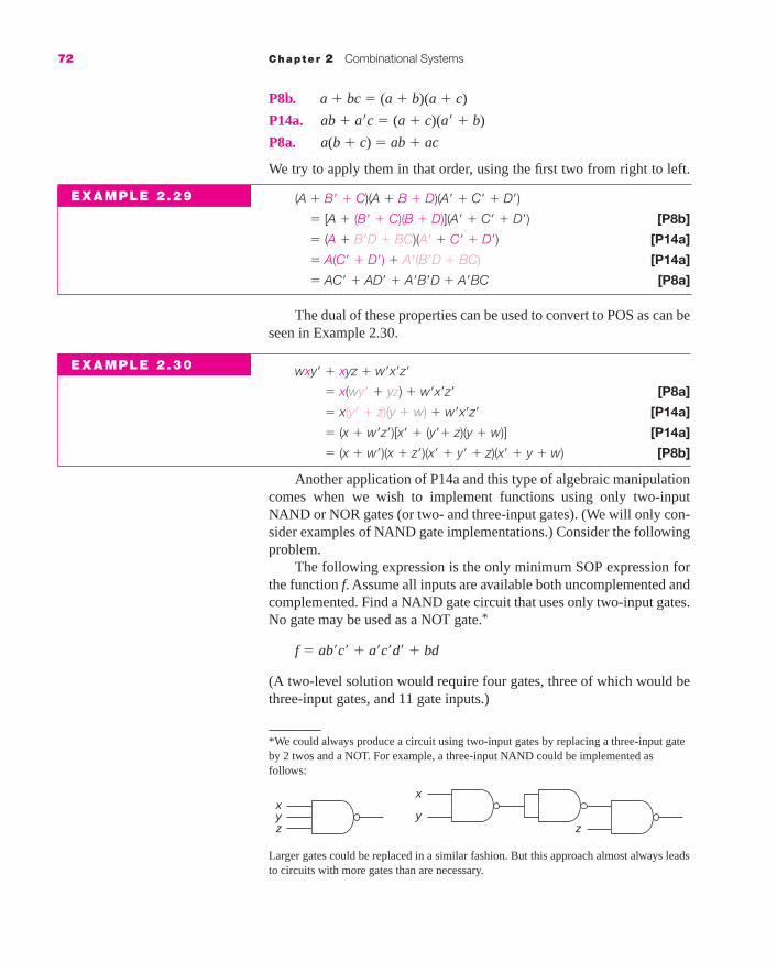
72 Chapter 2 Combinational Systems
P8b. a � bc � (a � b)(a � c)
P14a. ab � a�c � (a � c)(a� � b)
P8a. a(b � c) � ab � ac
We try to apply them in that order, using the first two from right to left.
(A � B� � C)(A � B � D)(A� � C� � D�)
� [A � (B� � C)(B � D)](A� � C� � D�) [P8b]
� (A � B�D � BC)(A� � C� � D�) [P14a]
� A(C� � D�) � A�(B�D � BC) [P14a]
� AC� � AD� � A�B�D � A�BC [P8a]
The dual of these properties can be used to convert to POS as can beseen in Example 2.30.
wxy� � xyz � w�x�z�
� x(wy� � yz) � w�x�z� [P8a]
� x(y� � z)(y � w) � w�x�z� [P14a]
� (x � w�z�)[x� � (y�� z)(y � w)] [P14a]
� (x � w�)(x � z�)(x� � y� � z)(x� � y � w) [P8b]
Another application of P14a and this type of algebraic manipulationcomes when we wish to implement functions using only two-inputNAND or NOR gates (or two- and three-input gates). (We will only con-sider examples of NAND gate implementations.) Consider the followingproblem.
The following expression is the only minimum SOP expression forthe function f. Assume all inputs are available both uncomplemented andcomplemented. Find a NAND gate circuit that uses only two-input gates.No gate may be used as a NOT gate.*
f � ab�c� � a�c�d� � bd
(A two-level solution would require four gates, three of which would bethree-input gates, and 11 gate inputs.)
*We could always produce a circuit using two-input gates by replacing a three-input gateby 2 twos and a NOT. For example, a three-input NAND could be implemented asfollows:
xyz z
x
y
Larger gates could be replaced in a similar fashion. But this approach almost always leadsto circuits with more gates than are necessary.
EXAMPLE 2.29
EXAMPLE 2.30
mar91647_c02_029_110.qxd 10/22/08 12:56 PM Page 72

2.8 Manipulation of Algebraic Functions and NAND Gate Implementations 73
More complex examples of finding a two-input gate implementationoften require the use of P14a as well as P8a. Consider the function inExamples 2.31 and 2.32 (already in minimum sum of products form).
f = w�y�z + wz� + wx + wy
We cannot factor anything from the three-literal term (since there is no w�,y�, or z in the other terms). We can factor w from any two of the others (notall three because that would leave a term z�+ x + y).
f = (w�y�z + wz�) + w(x + y)
We can then use Property 14. One of the solutions is
f = (w� + z�)(w + y�z) + w(x + y)
Figure 2.22 A two-input NAND gate circuit.
a
c�
fb
d
a�
d�
b�
EXAMPLE 2.31
To solve this problem, we must eliminate three-input gates. Thus,the starting point is to attempt to factor something from the three literalterms. In this example, there is a common c� in the first two terms, andwe can thus obtain
f � c�(ab� � a�d�) � bd
This, indeed, solves the whole problem in one step because not only didwe reduce the 2 three-input product terms to two inputs each, but we alsogot the final OR to a two-input one. Thus, the resulting circuit is shownin Figure 2.22, where we first implemented it with AND and OR gatesand then, starting at the output, added double inverters in each path fromthe input of an OR back to the output of an AND. (In this example, noinputs came directly into an OR.) This solution requires 6 gates and 12inputs. It should be noted that either solution, this one or the two-levelone mentioned earlier requires two integrated circuit packages. Thisrequires two 7400s (4 two-input NANDs each) and would leave two ofthe gates unused. The two-level solution would require a 7410 (3 three-input gates) and a 7400 for the remaining two-input gate and would leavethree of those gates unused. (If we had replaced each three-input gate by2 two-input ones plus a NOT, the implementation would require 7 two-input gates plus three NOT gates.)
mar91647_c02_029_110.qxd 10/22/08 12:56 PM Page 73

74 Chapter 2 Combinational Systems
G � DE� � A�B�C� � CD�E � ABC�E
The four-literal product term is the first place we must attack. We could fac-tor E from the last two terms. That would produce
G � DE� � A�B�C� � E(CD� � ABC�)
But now, there is no way of eliminating the three-input gate correspondingto A�B�C�. Instead, we can factor C� from the second and the fourth terms,producing
G � C�(A�B� � ABE) � DE� � CD�E
We can apply P14a to the expression within the parentheses to get
G � C�(A� � BE)(A � B�) � DE� � CD�E
or, using B instead of A,
G � C�(B� � AE)(B � A�) � DE� � CD�E
In either case, we still have 2 three-input AND terms, that first product andthe last one. (We cannot take the output of the OR gate that forms B� � AEand the output of the OR gate that forms B � A� and connect them to atwo-input AND gate. We would then need to connect the output of thatAND gate to the input of another AND gate with C� as its other input. Thiswould violate the third rule for conversion to NAND gates—the inputs toAND gates may not come from the output of another AND gate.) We canreduce it to all two-input gates by applying P14a again, using the C� fromthe first complex term and the C from the last product term, producing (fromthe second version) the following expression:
G � (C� � D�E)[C � (B� � AE)(B � A�)] � DE�
This requires 10 gates, as shown in the following NAND gate circuit.
EXAMPLE 2.32
ww
xx �
yy �
w �
z �
w
z
z
y �w
f
The circuit implementing this is shown below, where the crossed out inputswere those that would have been into an OR.
mar91647_c02_029_110.qxd 10/22/08 12:56 PM Page 74

2.8 Manipulation of Algebraic Functions and NAND Gate Implementations 75
Again, we began by implementing the circuit with ANDs and ORs, startingat the innermost parentheses. Five of the inputs went directly to OR gatesand were thus complemented (as shown in brown in the circuit).
There is still another approach to manipulating this algebra.
G � C�(A� � BE)(A � B�) � DE� � CD�E
� C�(A� � BE)(A � B�) � (D � CE)(D� � E�)
� (A� � BE)(AC� � B�C�) � (D � CE)(D� � E�)
In this case, we eliminated the three-input AND by distributing the C� (P8a)and used P14a on the last two product terms. We will leave the implemen-tation of this as an exercise, but we can count 11 gates (one more thanbefore) from the algebraic expression, as seen from the following count.
G � (A� � BE )(AC� � B�C�) � (D � CE )(D� � E�)
1 2 3 4 5 6 7 8 9 10 11
where each gate is numbered below the operator corresponding to that gate.
As an example of sharing a gate, consider the implementation of thefollowing function with two-input NAND gates:
G � C�D� � ABC� � A�C � B�C
� C�(D� � AB) � C(A� � B�)
The circuit for that expression is shown next.
G
D
E �
D �
C �
E
C
A
E
B
B �
A
C �D
C
GB
A
EXAMPLE 2.33
mar91647_c02_029_110.qxd 10/22/08 12:56 PM Page 75

76 Chapter 2 Combinational Systems
EXAMPLE 2.34
*We could just as easily factor b and b� or a and a� from these expressions; the resultingcircuits would have the same layout of gates.
Note that only one NAND gate is needed for the product term AB andfor the sum term A� � B� (because inputs coming directly to an OR arecomplemented).
As a final example, we will return to the implementation of the fulladder (CE3). The SOP expressions developed in Example 2.11 arerepeated (where the carry input, cin, is represented by just c).
s � a�b�c � a�bc� � ab�c� � abc
cout � bc � ac � ab
A two-level implementation of these would require 1 four-input NANDgate (for s), 5 three-input NAND gates (four for s and one for cout), and 3 two-input NANDs (for cout), assuming all inputs are available both uncom-plemented and complemented. But this assumption is surely not valid for cbecause that is just the output of combinational logic just like this (from thenext less significant bit of the sum). Thus, we need at least one NOT gate(for c�) and possibly three (one for each input). The implementation of thisadder would thus require four integrated circuit packages (one 7420, two7410s, and one 7400). (There would be one gate left over of each size,which could be used to create whatever NOTs are needed.)
Although s and cout are in minimum SOP form, we can manipulate thealgebra to reduce the gate requirements by first factoring c from two termsof s and from two terms of cout, and factoring c� from the other two terms ofs, yielding*
s � c(a�b� � ab) � c�(ab� � a�b)
cout � c(a � b) � ab
This requires 11 two-input NAND gates, not including the three NOTs(because ab need only be implemented once for the two terms and a � bis implemented using the same gate as a�b�).
Returning to the expression for sum, note that
s � c(a � b)� � c�(a � b) � c � (a � b)
Furthermore, we could write
cout � c(a � b) � ab
(That is a little algebraic trick that is not obvious from any of the properties.However, the difference between a � b and a � b is that the former is
mar91647_c02_029_110.qxd 10/22/08 12:56 PM Page 76

2.8 Manipulation of Algebraic Functions and NAND Gate Implementations 77
1 when both a and b are 1, but the latter is not. But the expression for cout
is 1 for a � b � 1 because of the ab term.)Using these last two expressions, we could implement both the sum
and carry using two Exclusive-ORs and 3 two-input NANDs as follows:
cb s
cout
a
a
b s
c
cout
Packages with four Exclusive-OR gates are available (7486) and thusthis circuit could be implemented with one of those packages and one 7400.Note that complemented inputs are not necessary for this implementation.
Finally, because we can implement each Exclusive-OR with 4 two-input NAND gates, without requiring complemented inputs, we obtain
Note that the two brown NAND gates have the same inputs and the two tanones also have the same inputs. Only one copy of each is necessary, yield-ing the final circuit with only nine NAND gates.
mar91647_c02_029_110.qxd 10/22/08 12:56 PM Page 77

78 Chapter 2 Combinational Systems
[SP 19, 20, 21, 22, 23, 24;EX 22, 23, 24, 25, 26, 27; LAB]
a
b s
c
cout
This implementation would require three 7400s if we were only building onebit of an adder. However, a 4-bit adder could be built with nine packages(36 two-input gates).
2.9 A MORE GENERAL BOOLEAN ALGEBRA
The basis for switching algebra is Boolean algebra, first published byGeorge Boole in 1849. It allows more than two elements. It is defined interms of a set of postulates and then the remaining properties are devel-oped from them as theorems. The postulates have been stated in a varietyof ways, but the following development seems most straightforward.Indeed, several of these postulates are identical in form to the propertiesof switching algebra listed in Sections 2.2.1 and 2.2.2. But there, webegan with the definition of the operators (limited to a two-valued alge-bra) and proved the properties either directly from the definition or byway of a truth table. Here, the operators are not defined, but can bederived from the postulates.
1. A Boolean algebra consists of a set of k � 2 elements. (For theswitching algebra developed in Section 2.2.1, k � 2.)
2. There are two binary operators, � and �, and one unaryoperator, �.
3. The algebra is closed, that is, if a and b are members of the set,then
a � b, a � b, a�
are also members of the set. (This property is not true of alloperators and all sets in normal algebra. For example, if the set isthe set of positive integers, subtraction is not closed since it may
mar91647_c02_029_110.qxd 10/22/08 12:56 PM Page 78

2.9 A More General Boolean Algebra 79
result in a negative integer, and division is not closed since the quo-tient may be a noninteger.)
4. Commutative law (same as P1):
i. a � b � b � a
ii. a � b � b � a
5. Associative law (same as P2):
i. a � (b � c) � (a � b) � c
ii. a � (b � c) � (a � b) � c
6. Distributive law (same as P8):
i. a � b � c � (a � b) � (a � c)
ii. a � (b � c) � a � b � a � c
7. Identity (similar to P3):
i. There exists a unique element in the set, 0, such thata � 0 � a
ii. There exists a unique element in the set, 1, such that a � 1 � a
8. Complement (same as P5): For each element a, there exists aunique element a� such that
i. a � a� � 1
ii. a � a� � 0
We have now defined Boolean algebra. It works for a two-valuedsystem (the switching algebra we have been discussing throughout thischapter) as well as a more general one.
For switching algebra, we can use these postulates to define theoperators. First, we can recognize that there are the two elements, 0 and1, postulated in number 7. Using that postulate and the commutative law,we can complete the first three lines of Table 2.16a for the OR (�) oper-ator and the last three for the AND(�). For the OR, the postulate
a � 0 � a
implies that 0 � 0 � 0 (first line) and 1 � 0 � 1 (third line). In addition,using the commutative law, we get
0 � a � a
and thus the second line is completed (0 � 1 � 1). Using the other part of postulate 7, we get 0 � 1 � 0, 1 � 1 � 1, and
with the commutative property, 1 � 0 � 0. For the remaining lines, weneed to prove the idempotency property (P6 from before). We can do thatin the following steps:
Table 2.16a Defining ORand AND.
a b a � b a � b
0 0 00 1 1 01 0 1 01 1 1
mar91647_c02_029_110.qxd 10/22/08 12:56 PM Page 79

80 Chapter 2 Combinational Systems
a � a � (a � a) � 1 [7ii]� (a � a) � (a � a�) [8i]� a � a � a� [6i]� a � 0 [8ii]� a [7i]
Using this theorem, we can complete the first row of the OR truth table (0 � 0 � 0). We can prove the dual of this theorem,
a � a � a
using the other half of each of the postulates and thus complete the lastline of the AND Table 2.16b (1 � 1 � 1).
Finally, we can define the NOT (�) operator from postulate 8. Part isays that either a or a� (or both) is 1; part ii says that either a or a� (orboth) is 0. Thus, one of them must be 1 and the other 0, that is, if a � 0,then a� must be 1, and if a � 1, then a� must be 0.
From here, we can prove all of the properties of switching algebra asbefore. Most of them are also properties of a general Boolean algebra,but that is beyond the scope of this book.
2.10 SOLVED PROBLEMS
1. For each of the following problems, there are four inputs, A, B,C, and D. Show a truth table for the functions specified. (Onetruth table with four outputs is shown for the four examples.)
a. The inputs represent a 4-bit unsigned binary number. Theoutput, W, is 1 if and only if the number is a multiple of 2 or of 3 but not both.
b. The inputs represent a 4-bit positive binary number. Theoutput, X, is 0 if and only if the input is a prime (where 0 never occurs).
c. The first two inputs (A, B) represent a 2-bit unsigned binarynumber (in the range 0 to 3). The last two (C, D) represent asecond unsigned binary number (in the same range). Theoutput, Y, is 1 if and only if the two numbers differ by two ormore.
d. The inputs represent a BCD number in Excess-3 code. Thosecombinations that do not represent one of the digits neveroccur. The output, Z, is 1 if and only if that number is a per-fect square.
The truth table contains the answer to all four parts.
Table 2.16b Completeddefinition of ORand AND.
a b a � b a � b
0 0 0 00 1 1 01 0 1 01 1 1 1
mar91647_c02_029_110.qxd 10/22/08 12:56 PM Page 80

2.10 Solved Problems 81
a. It doesn’t matter whether one considers 0 a multiple of 2 or 3because it is either a multiple of neither or of both. In bothcases, W � 0. For the next row, 1 is not a multiple of either 2or 3; thus, W � 0. For the next three rows W � 1 because 2and 4 are multiples of 2, but not 3, and 3 is a multiple of 3, butnot 2. Both 5 and 7 are multiples of neither and 6 is a multipleof both; thus, for the next three rows, W � 0. Then, 8, 10, and14 are multiples of only 2; 9 and 15 are multiples of only 3; allof these produce an output of 1. The others produce an outputof 0 (12 is a multiple of both 2 and 3).
b. A prime number is one that is evenly divisible only by 1 oritself. Note that the problem specifies that the output is 0 forprimes and is thus 1 for numbers that are not prime. The firstnonprime is 4 (2 � 2). Indeed, all of the even numbers (otherthan 2) are nonprimes. Because 0 never occurs, the output forthe first row is a don’t care.
c. For the first four rows, the first number is 0. It is compared onsuccessive rows with 0, 1, 2, and 3. Only 2 and 3 differ from 0by 2 or more. In the next group of four rows, the first numberis 1; it only differs from 3 by 2 or more. In the next four rows,2 differs only from 0 by 2 or more. Finally, in the last 4 rows,3 differs from 0 and 1 by 2 or more.
d. A perfect square is an integer obtained by multiplying someinteger by itself. Thus, 0, 1, 4, and 9 are perfect squares. Notethat the first three rows and the last three rows are all don’tcares because those input combinations never occur.
2. The system is a speed warning device. It receives, on two lines, anindication of the speed limit on the highway. There are three
A B C D W X Y Z
0 0 0 0 0 X 0 X0 0 0 1 0 0 0 X0 0 1 0 1 0 1 X0 0 1 1 1 0 1 10 1 0 0 1 1 0 10 1 0 1 0 0 0 00 1 1 0 0 1 0 00 1 1 1 0 0 1 11 0 0 0 1 1 1 01 0 0 1 1 1 0 01 0 1 0 1 1 0 01 0 1 1 0 0 0 01 1 0 0 0 1 1 11 1 0 1 0 0 1 X1 1 1 0 1 1 0 X1 1 1 1 1 1 0 X
mar91647_c02_029_110.qxd 10/22/08 12:56 PM Page 81

Speed c d
�45 0 046–55 0 156–65 1 0�65 1 1
Speed limit a b
45 0 055 0 165 1 0
unused 1 1
The outputs will be 1 if the car is speeding or driving dangerously.a b c d f g
0 0 0 0 0 045 0 0 0 1 1 0
0 0 1 0 1 10 0 1 1 1 1
0 1 0 0 0 055 0 1 0 1 0 0
0 1 1 0 1 00 1 1 1 1 1
1 0 0 0 0 065 1 0 0 1 0 0
1 0 1 0 0 01 0 1 1 1 1
1 1 0 0 X X1 1 0 1 X X1 1 1 0 X X1 1 1 1 X X
3. Show a block diagram of a circuit using AND and OR gates foreach side of P8b: a � bc � (a � b)(a � c)
a
b
a
c
(a � b) (a � c)
a
b
c
a � bc
possible values: 45, 55, or 65 mph. It receives from the automobile,on two other lines, an indication of the speed of the vehicle. Thereare four possible values: under 45, between 46 and 55, between 56and 65, and over 65 mph. It produces two outputs. The first, f,indicates whether the car is going above the speed limit. Thesecond, g, indicates that the car is driving at a “dangerous speed”—defined as either over 65 mph or more than 10 mph above thespeed limit. Show how each of the inputs and outputs are coded (interms of binary values) and complete the truth table for this system.
The first step is to code the inputs. We chose (arbitrarily) what isshown in the following tables.
82 Chapter 2 Combinational Systems
mar91647_c02_029_110.qxd 10/22/08 12:56 PM Page 82

2.10 Solved Problems 83
XYZ XY� YZ X�Y�Z� F XYZ X�Y X � Z� Y � Z () ( ) G
000 0 0 1 1 000 0 1 0 0 0001 0 0 0 0 001 0 0 1 0 0010 0 0 0 0 010 1 1 1 1 1011 0 1 0 1 011 1 0 1 0 1100 1 0 0 1 100 0 1 0 0 0101 1 0 0 1 101 0 1 1 1 1110 0 0 0 0 110 0 1 1 1 1111 0 1 0 1 111 0 1 1 1 1
5. Determine, using truth tables, whether or not each of the groupsof expressions are equal:
a. f � a�c� � a�b � ac
g � bc � ac � a�c�
b. f � P�Q� � PR � Q�R
g � Q� � PQR
(a)
abc a�c� a�b ac f bc ac a�c� g
000 1 0 0 1 0 0 1 1001 0 0 0 0 0 0 0 0010 1 1 0 1 0 0 1 1011 0 1 0 1 1 0 0 1100 0 0 0 0 0 0 0 0101 0 0 1 1 0 1 0 1110 0 0 0 0 0 0 0 0111 0 0 1 1 1 1 0 1
The two functions are equal.
(b)
←
PQR P�Q� PR Q�R f Q� PQR g
000 1 0 0 1 1 0 1001 1 0 1 1 1 0 1010 0 0 0 0 0 0 0011 0 0 0 0 0 0 0100 0 0 0 0 1 0 1101 0 1 1 1 1 0 1110 0 0 0 0 0 0 0111 0 1 0 1 0 1 1
4. Show a truth table for the following functions:
a. F � XY� � YZ � X�Y�Z�
b. G � X�Y � (X � Z�)(Y � Z)
(a) (b)
mar91647_c02_029_110.qxd 10/22/08 12:56 PM Page 83

84 Chapter 2 Combinational Systems
Note that for row 100 (marked with a brown arrow), f � 0 andg � 1. Thus, the two functions are different.
6. For each of the following expressions, indicate which (if any) ofthe following apply (more than one may apply):
i. Product term
ii. Sum of products expression
iii. Sum term
iv. Product of sums expression
a. ab�
b. a�b � ad
c. (a � b)(c � a�d)
d. a� � b�
e. (a � b�)(b � c)(a� � c � d)
a. i. product of two literals
ii. sum of one product term
iv. product of two sum terms
b. ii. sum of two product terms
c. none; second term is not a sum term
d. ii. sum of two product terms
iii. sum of two literals
iv. product of one sum term
e. iv. product of three sum terms
7. In the expressions of problem 6, how many literals are in each?
a. 2 b. 4 c. 5 d. 2 e. 7
8. Using Properties 1 to 10, reduce the following expressions to aminimum SOP form. Show each step (number of terms andnumber of literals in minimum shown in parentheses).
a. xyz� � xyz (1 term, 2 literals)
b. x�y�z� � x�y�z � x�yz � xy�z � xyz (2 terms, 3 literals)
c. f � abc� � ab�c � a�bc � abc (3 terms, 6 literals)
a. xyz� � xyz � xy (z� � z) � xy � 1 � xy [P8a, P5aa, P3b]or, in one step, using P9a, where a � xy and b � z�
mar91647_c02_029_110.qxd 10/22/08 12:56 PM Page 84

2.10 Solved Problems 85
b. x�y�z� � x�y�z � x�yz � xy�z � xyz
Make two copies of x�y�z� �x�y�z� � x�y�z� � �x�y�z � x�yz� � �xy�z � xyz� [P6a]� x�y��z� � z� � x�z�y� � y� � xz�y� � y� [P8a]� x�y� � 1 � x�z � 1 � xz � 1 [P5aa]� x�y� � x�z � xz [P3b]� x�y� � �x� � x�z � x�y� � 1 � z [P8a, P5aa]� x�y� � z [P3bb]
or, without using P6a,� (x�y�z� � x�y�z) � x�yz � (xy�z � xyz)� x�y� � x�yz � xz [P9a]� x�(y� � yz) � xz [P8a]� x�(y� � z) � xz [P10a]� x�y� � x�z � xz [P8a]� x�y� � z [P9a]
Note that we could follow a path that does not lead us to thecorrect answer, by combining the last two terms in the secondline of this second sequence, yielding
� x�y� � z(x�y � x)� x�y� � z(y � x) [P10a]� x�y� � yz � xz [P8a]
This is a dead end. It has more terms than the minimum (whichwas given) and we do not have the tools (in Properties 1 to 10)to reduce this further without backing up to the originalexpression (or, at least, the first reduction). We should then goback and start again.
c. There are two approaches to this problem. In the first, we notethat abc can be combined with each of the other terms. Thus,we make three copies of it, usingabc � abc � abc � abc [P6a]
f � (abc� � abc) � (ab�c � abc) � (a�bc � abc)� ab � ac � bc [P9a]
In the second approach, we just use abc to combine with theterm next to it, producingf � abc� � ab�c � a�bc � abc � abc� � ab�c � bc [P9a]
� abc� � c(b � b�a) � abc� � c(b � a)� abc� � bc � ac [P10a]� a(c � c�b) � bc � a(c � b) � bc� ac � ab � bc [P10a]
or, in place of the last two lines,
mar91647_c02_029_110.qxd 10/22/08 12:56 PM Page 85

86 Chapter 2 Combinational Systems
� b(c � c�a) � ac � b(c � a) � ac
� bc � ab � ac [P10a]In this approach, we used P10a twice to eliminate a literal fromthe second term and then the first. We could have done it in anyorder. Indeed, there were two ways to do the last step (as shownon the last two lines).
9. Using Properties 1 to 10, reduce the following expressions to aminimum POS form. Show each step (number of terms andnumber of literals in parentheses).
a. (a � b� � c) (a � b� � c�) (a� � b � c) (a� � b� � c)(2 terms, 4 literals)
b. (x� � y� � z�) (x� � y � z�) (x� � y � z) (2 terms, 4 literals)
a. We group the first two and the last two terms, and use Property 9b
[(a � b� � c)(a � b� � c�)][(a� � b � c)(a� � b� � c)] �
[a � b�][a� � c]
b. We can make a second copy of the middle term and group itwith each of the others
(x� � y� � z�)(x� � y � z�)(x� � y � z)
� [(x� � y� � z�)(x� � y � z�)][(x� � y � z)(x� � y � z�)]
� [x� � z�][x� � y]
If we don’t make the second copy, we get
[x� � z�](x� � y � z)
We can then use P8b to get
x� � z� (y � z) � x� � yz� [P8a, P5bb, P3a]� (x� � y)(x� � z) [P8b]
10. Show a block diagram of a system using AND, OR, and NOT gatesto implement the following function. Assume that variables areavailable only uncomplemented. Do not manipulate the algebra.
F � [A (B � C)� � BDE](A� � CE)
B
E
B
C
D
A
A
F
C
E
mar91647_c02_029_110.qxd 10/22/08 12:56 PM Page 86
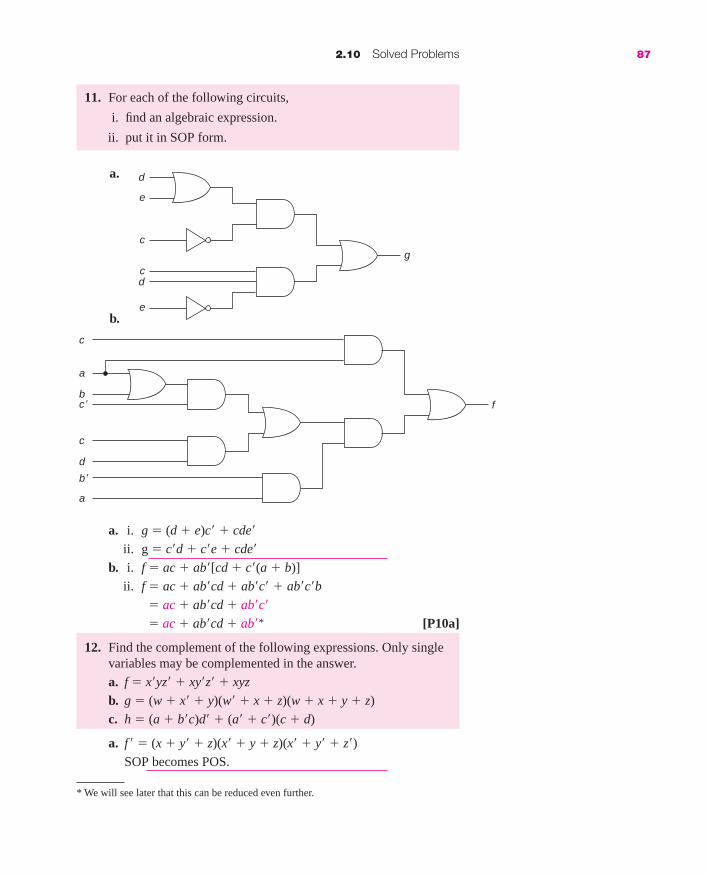
2.10 Solved Problems 87
11. For each of the following circuits,
i. find an algebraic expression.
ii. put it in SOP form.
* We will see later that this can be reduced even further.
d
e
c
cd
e
g
c
f
a
bc�
c
d
b�
a
a. i. g � (d � e)c� � cde�
ii. g � c�d � c�e � cde�
b. i. f � ac � ab�[cd � c�(a � b)]
ii. f � ac � ab�cd � ab�c� � ab�c�b
� ac � ab�cd � ab�c�
� ac � ab�cd � ab�* [P10a]
12. Find the complement of the following expressions. Only singlevariables may be complemented in the answer.
a. f � x�yz� � xy�z� � xyz
b. g � (w � x� � y)(w� � x � z)(w � x � y � z)
c. h � (a � b�c)d� � (a� � c�)(c � d)
a. f � � (x � y� � z)(x� � y � z)(x� � y� � z�)
SOP becomes POS.
a.
b.
mar91647_c02_029_110.qxd 10/22/08 12:56 PM Page 87
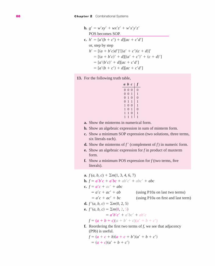
88 Chapter 2 Combinational Systems
b. g� � w�xy� � wx�z� � w�x�y�z�
POS becomes SOP.
c. h� � [a�(b � c�) � d][ac � c�d�]
or, step by step
h� � [�a � b�c�d�]�[�a� � c���c � d�]�� [�a � b�c�� � d][�a� � c��� � �c � d��]� [a��b�c�� � d][ac � c�d�]
� [a��b � c�� � d][ac � c�d�]
13. For the following truth table,
a. Show the minterms in numerical form.
b. Show an algebraic expression in sum of minterm form.
c. Show a minimum SOP expression (two solutions, three terms,six literals each).
d. Show the minterms of f � (complement of f ) in numeric form.
e. Show an algebraic expression for f in product of maxtermform.
f. Show a minimum POS expression for f (two terms, fiveliterals).
a. f (a, b, c) � �m(1, 3, 4, 6, 7)
b. f � a�b�c � a�bc � ab�c� � abc� � abc
c. f � a�c � ac� � abc
� a�c � ac� � ab (using P10a on last two terms)
� a�c � ac� � bc (using P10a on first and last term)
d. f ��a, b, c� � �m�0, 2, 5�e. f ��a, b, c� � �m�0, 2, 5�
� a�b�c� � a�bc� � ab�c
f � (a � b � c)(a � b� � c)(a� � b � c�)
f. Reordering the first two terms of f, we see that adjacency(P9b) is useful.
f � �a � c � b��a � c � b���a� � b � c��� �a � c��a� � b � c��
a b c f
0 0 0 00 0 1 10 1 0 00 1 1 11 0 0 11 0 1 01 1 0 11 1 1 1
mar91647_c02_029_110.qxd 10/22/08 12:56 PM Page 88

2.10 Solved Problems 89
a.
b. f � x�yz� � x�yz � xy�z � xyz� � xyzc. f � x�y � xy�z � xy
� y � xy�z� y � xz
d. f ��x, y, z� � �m�0, 1, 4�e. f � � x�y�z� � x�y�z � xy�z�
f � (x � y � z) (x � y � z�)(x� � y � z)f. f � � x�y�z� � x�y�z � xy�z� � x�y�z�
� x�y� � y�z�
f � (x � y) (y � z)
15. Show a block diagram corresponding to each of the expressionsbelow using only NAND gates. Assume all inputs are availableboth uncomplemented and complemented. There is no need tomanipulate the functions to simplify the algebra.
a. f � ab�d� � bde� � bc�d � a�ce
b. g � b(c�d � c�e�) � (a � ce) (a� � b�d�)
Or, we can minimize f � and then use DeMorgan’s theorem:
f � � a�c� � ab�c
f � (a � c)(a� � b � c�)
14. For the following function,
f (x, y, z) � �m(2, 3, 5, 6, 7)
a. Show the truth table.
b. Show an algebraic expression for f in sum of minterm form.
c. Show a minimum SOP expression for f (two terms, threeliterals).
d. Show the minterms of f � (complement of f ) in numeric form.
e. Show an algebraic expression for f in product of maxtermform.
f. Show a minimum POS expression for f (two terms, fiveliterals).
x y z f
0 0 0 00 0 1 00 1 0 10 1 1 11 0 0 01 0 1 11 1 0 11 1 1 1
mar91647_c02_029_110.qxd 10/22/08 12:56 PM Page 89

90 Chapter 2 Combinational Systems
ab �
f
a �ce
d �
b
b
d
d
e �
c �
ga �
c �
d
c
e
ab �
d �
c �
e� b
(b)(a)
Note that in part (a), this is a two-level circuit. In part (b), theonly inputs that go directly into an OR are a and a�; they arecomplemented.
16. Show a block diagram corresponding to each of the followingexpressions using only NOR gates. Assume all inputs areavailable both uncomplemented and complemented. There is noneed to manipulate the functions to simplify the algebra.
a. f � (a � b�)(a� � c � d)(b � d�)
b. g � [a�b� � a(c � d)](b � d�)
a
a�c fd
b
d �
b �
b
g
d �
d
c
b�
a�
a
b
a
a�
(b)(a)
17. For each of the following circuits,
i. Find an algebraic expression.
ii. Put it in minimum SOP form.
mar91647_c02_029_110.qxd 10/22/08 12:56 PM Page 90

2.10 Solved Problems 91
a. i. f � (a � b) � (a � c�)
ii. f � �a�b � ab�� � �a�c� � ac�� �a�b � ab��� �a�c� � ac�� �a�b � ab�� �a�c� � ac��� �a�b� � ab� �a�c� � ac� � �a�b � ab���a�c � ac��� a�b�c� � abc � a�bc � ab�c�
� b�c� � bc
b. i. g � x� � y� � �a�b � ab��� � c � d
ii. g � ab � a�b� � c � d
c. i. f � {[(a� � b)� � c](c�d)�}� � [(b(c�d)�]�
ii. f � {[�a� � b�� � c]� � �c�d�} � [b� � c�d]
� �a� � b�c� � c�d � b� � c�d
� a�c� � bc� � c�d � b� � a�c� � c� � c�d � b�
� c� � a�c� � c�d� � b� � c� � b�
18. Reduce the following expressions to a minimum SOP form.Show each step (number of terms and number of literals inminimum shown in parentheses).
a. F � A � B � A�B�C�D (3 terms, 4 literals)
b. f � x�y�z � w�xz � wxyz� � wxz � w�xyz(3 terms, 7 literals)
c. g � wxy� � xyz � wx�yz � xyz� � wy�
(3 terms, 6 literals)
a
f
a
c �
b
(a) (b)
a
g
c
x
yd
b
(c)
a�
bc
fc �
d
b
mar91647_c02_029_110.qxd 10/22/08 12:56 PM Page 91

92 Chapter 2 Combinational Systems
d. H � AB � B�C � ACD � ABD� � ACD�(2 terms, 4 literals)
e. G � ABC� � A�C�D � AB�C� � BC�D � A�D(2 terms, 4 literals)
f. f � abc � b�cd � acd � abd�(2 solutions, 3 terms, 9 literals)
a. F � A � B � A�B�C�D
� �A � A�B�C�D� � B
� �A � B�C�D� � B [P10a]� A � �B � B�C�D�� A � B � C�D [P10a]
We can also achieve the same result using a different approach.
A � B � A�B�C�D � �A � B� � �A � B��C�D [P11a]� �A � B� � C�D [P10a]
b. f � x�y�z � w�xz � wxyz� � wxz � w�xyz
� x�y�z � w�xz � wxyz� � wxz [P12a]� x�y�z � xz � wxyz� [P9a]� x�y�z � x�z � wyz��� x�y�z � x�z � wy� [P10a]� x�y�z � xz � wxy
� z�x�y� � x� � wxy
� z�y� � x� � wxy [P10a]� y�z � xz � wxy
c. There are two ways to apply P10a. If we use it with the firstand third terms, we get
g � w(y� � yx�z) � xy
� w(y� � x�z) � xy
� wy� � wx�z � xy
But now, there is nothing further we can do (without a great dealof backtracking or P13a).
However, if we first used P10a with the second and third terms,
g � wy� � y(x � x�wz)
� wy� � y(x � wz)
� wy� � xy � wyz
Now we can apply P10a again to the first and third terms toproduce the solution with six literals.
g � w(y� � yz) � xy � w(y� � z) � xy � wy� � wz � xy
mar91647_c02_029_110.qxd 10/22/08 12:56 PM Page 92
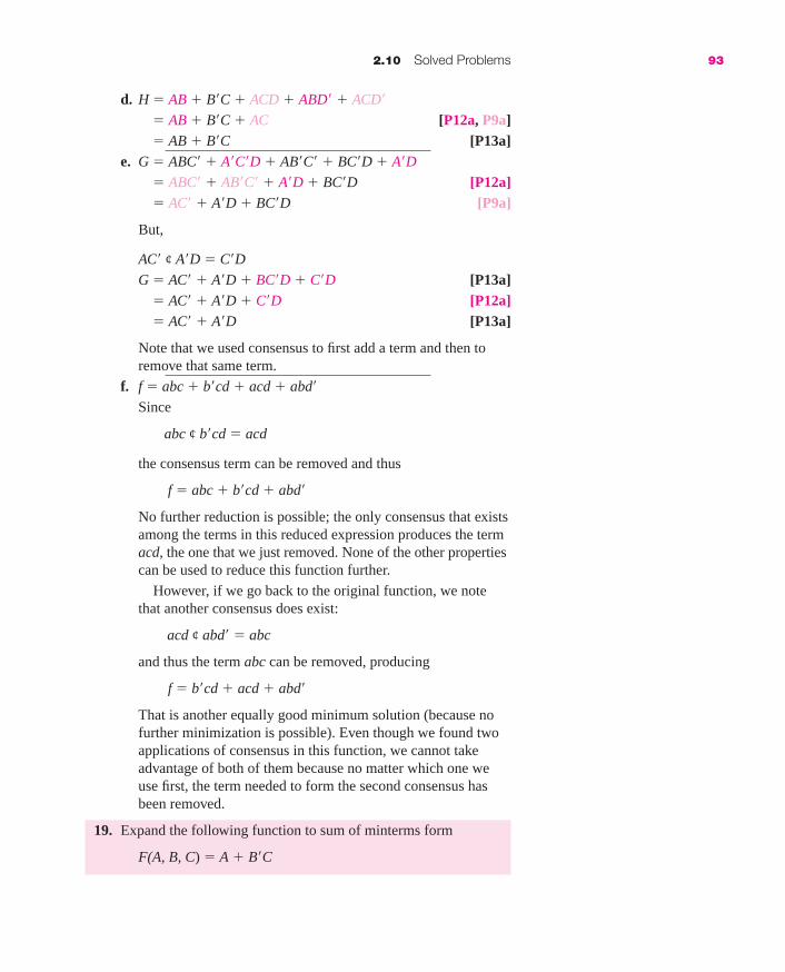
2.10 Solved Problems 93
the consensus term can be removed and thus
f � abc � b�cd � abd�
No further reduction is possible; the only consensus that existsamong the terms in this reduced expression produces the termacd, the one that we just removed. None of the other propertiescan be used to reduce this function further.
However, if we go back to the original function, we notethat another consensus does exist:
acd ¢ abd� � abc
and thus the term abc can be removed, producing
f � b�cd � acd � abd�
That is another equally good minimum solution (because nofurther minimization is possible). Even though we found twoapplications of consensus in this function, we cannot takeadvantage of both of them because no matter which one weuse first, the term needed to form the second consensus hasbeen removed.
19. Expand the following function to sum of minterms form
F(A, B, C) � A � B�C
d. H � AB � B�C � ACD � ABD� � ACD�
� AB � B�C � AC [P12a, P9a]� AB � B�C [P13a]
e. G � ABC� � A�C�D � AB�C� � BC�D � A�D
� ABC� � AB�C� � A�D � BC�D [P12a]� AC� � A�D � BC�D [P9a]
But,
AC� ¢ A�D � C�D
G � AC� � A�D � BC�D � C�D [P13a]� AC� � A�D � C�D [P12a]� AC� � A�D [P13a]
Note that we used consensus to first add a term and then toremove that same term.
f. f � abc � b�cd � acd � abd�
Since
abc ¢ b�cd � acd
mar91647_c02_029_110.qxd 12/16/08 2:41 PM Page 93

94 Chapter 2 Combinational Systems
We have a choice of two approaches. We could use P3b,P5aa (both from right to left) and P8a repeatedly to produce
A � B�C � A�B� � B� � �A� � A�B�C
� AB� � AB � A�B�C � AB�C
� AB��C� � C� � AB�C� � C� � A�B�C � AB�C
� AB�C� � AB�C � ABC� � ABC � A�B�C � AB�C
� AB�C� � AB�C � ABC� � ABC � A�B�C
having removed the duplicated term (AB�C). Or we could use atruth table, such as
A B C B�C F
0 0 0 0 00 0 1 1 10 1 0 0 00 1 1 0 01 0 0 0 11 0 1 1 11 1 0 0 11 1 1 0 1
and thus,
F � A�B�C � AB�C� � AB�C � ABC� � ABC
which is the same as the previous expression reordered, or
F (A, B, C) � �m(1, 4, 5, 6, 7)
20. Convert each of the following expressions to SOP form:
a. (w � x� � z)(w� � y � z�)(x � y � z)
b. (a � b � c � d�)(b � c � d)(b� � c�)
a. �w � x� � z��w� � y � z���x � y � z�� [z � �w � x���x � y�]�w� � y � z�� [P8b]� �z � wx � x�y��w� � y � z�� [P14a]� z�w� � y� � z��wx � x�y� [P14a]� w�z � yz � wxz� � x�yz� [P8a]
Note that this is not a minimum SOP expression, even thoughthe original was a minimum POS expression. Using P10a, wecould reduce this to
w�z � yz � wxz� � x�y
b. �a � b � c � d���b � c � d��b� � c��� [b � c � �a � d��d]�b� � c�� [P8b]� �b � c � ad��b� � c�� [P8b, P5b, P3a]
mar91647_c02_029_110.qxd 12/16/08 2:41 PM Page 94

2.10 Solved Problems 95
� bc� � b��c � ad� [P14a]� bc� � b�c � ab�d [P8a]
or using c instead of b for P14a
� �b � c � ad��b� � c��� b�c � c��b � ad�� b�c � bc� � ac�d
These are two equally good solutions.
21. Convert the following expression to POS form:
a�c�d � a�cd� � bc
a�c�d � a�cd� � bc
� c�b � a�d�� � c�a�d [P8a]� �c � a�d��c� � b � a�d�� [P14a]� �c � a���c � d��c� � b � a���c� � b � d�� [P8b]
Two comments are in order. This is not in minimum POS form.P12b allows us to manipulate the first and third terms so as toreplace the third term by (a� � b). We could have started theprocess by factoring a� from the first two terms, but that wouldrequire more work.
22. Implement each of the following expressions (which are alreadyin minimum SOP form) using only two-input NAND gates. No gate may be used as a NOT. All inputs are available bothuncomplemented and complemented. (The number of gatesrequired is shown in parentheses.)
a. f � w�y� � xyz � wyz� � x�y�z (8 gates)
b. f � abc � abd � a�c�d � a�b�c (8 gates)
c. F � B�C�D� � BD � ACD � ABC (7 gates)
d. g � a�b�c�d� � abcd� � a�ce � ab�d � be (12 gates)
a. f � y�(w� � x�z) � y(xz � wz�)
fw
x
z
x �
z
w
z � y
y �
mar91647_c02_029_110.qxd 10/22/08 12:56 PM Page 95

96 Chapter 2 Combinational Systems
b. f = abc + abd + a�c�d + a�b�cFactoring ab from the first two terms and a� from the second, weget
f = ab(c + d) + a�(c�d + b�c)
But that would require a three-input AND for the first term. Wecould distribute the a or b through the parentheses, getting
f = a(bc + bd) + a�(c�d + b�c)
That requires nine gates. Instead, we can factor c from the firstand last term, and d from the middle terms, yielding
f = c(ab + a�b�) + d(ab + a�c�)
Since the term ab appears twice, we can share that gate,producing
a�
b�
a�
c�
a
b
c
d
f
c. F = AC(B + D) + B�C�D� + BD= (C + B�D�)[C� + A(B + D)] + BD
F
D �
C �
C
A
B �
D
B
Note that the gate on the left is used to implement both the B�D�term and the (B � D) term.
d. g � a�b�c�d� � abcd� � a�ce � ab�d � be
The first attempt at a solution yields one with 13 gates.
mar91647_c02_029_110.qxd 10/22/08 12:56 PM Page 96

2.10 Solved Problems 97
g � d��a�b�c� � abc� � e�b � a�c� � ab�d
� �d� � ab���d � a�b�c� � abc� � e�b � a�c�� �d� � ab��[d � �a � b�c���a� � bc�] � e�b � a�c�
1 2 3 4 5 6 7 8 9 10 11 12 13
Another approach is
g � a��b�c�d� � ce� � a�bcd� � b�d� � be
� [a � b�c�d� � ce][a� � bcd� � b�d] � be
� [a � �c � b�d���c� � e�][a� � (b � d)�b� � cd��] � be
1 2 3 4 5 6 7 3 8 9 10 11 12
where gate three is used twice, as follows.
g
e
bd �
d �
c �
b �
e � a �
a
c
c
b
23. For the following function, show the block diagram for aNAND gate implementation that uses only four 7400 seriesNAND gate modules. No gate may be used as a NOT. Assumethat all variables are available both uncomplemented andcomplemented. (Note that a two-level solution would require2 six-input gates and a five-input gate (each of which would beimplemented with a 7430 module containing 1 eight-input gate),plus a 7420 for the four-input gate and a 7410 for the 2 three-input gates and the 1 two-input gate.)
g � abcdef � d�e�f � a�b� � c�d�e� � a�def� � abcd�f�
g � abc(def � d�f�) � d�e�(c� � f ) � a�(b� � def�)
This requires 1 four-input gate (for the first term), 4 three-inputgates, and 5 two-input gates (one 7420, with the second gateused as a three-input one, one 7410, and two 7400s with three
mar91647_c02_029_110.qxd 10/22/08 12:56 PM Page 97

98 Chapter 2 Combinational Systems
a�e
g
b�
abc
d �
d
c�
e �
f
a
f�
e
f
f�
gates unused). If we required that no four-input gates be used,we could further manipulate the algebra as follows:
g � [a� � bc(def � d�f �)][a � b� � def�] � d�e�(c� � f )
using P14a on the first and last terms, which would require 5 three-input gates and 6 two-input gates (still four modules).
We could also do a completely different factoring, yielding
g � de�abcf � a�f�� � d��abcf� � e�f � c�e�� � a�b�
� [d� � e�abcf � a�f ��][d � abcf �� e�f � c�e�] � a�b�
� [d� � e�a� � f�� f�� abc�]� [d � c�e� � � f � abc�� f � � e��] � a�b�
This requires 3 three-input gates and 10 two-input gates (alsofour modules), as shown below.
24. The following is already in minimum sum of products form.
F � B�DE� � A�B�D � A�BC�D� � ABD�E� � ABDE � ACDE
All variables are available both uncomplemented andcomplemented. Find two solutions, each of which uses no morethan three integrated circuit packages of NAND gates (4 two-input or 3 three-input or 2 four-input gates per package). Onesolution must use only two- and three-input gates; the other mustuse at least 1 four-input gate package.
The easiest starting point is to factor pairs of terms as follows:
F � B�D(A� � E�) � BD�(A�C� � AE�) � ADE(B � C)
mar91647_c02_029_110.qxd 12/16/08 2:41 PM Page 98

2.10 Solved Problems 99
This indeed corresponds to a solution that satisfies the problemrequirements. There are 3 three-input gates (corresponding to thefirst AND of B�D ( ), the second AND of BD� ( ), and the outputOR). There is 1 four-input gate, corresponding to the last AND,and 5 two-input gates. We thus need one 7420 for the four-inputgate; the second gate on that package can be used as the fifth two-input gate. The 3 three-input gates require one 7410, and theremaining 4 two-input gates require one 7400.
By utilizing P14a, we obtain
F � B�D(A� � E�) � BD�(A�� E�)(A � C�) � ADE(B � C )
Note that the term A� � E� appears twice in the expression, andwe can thus share the output of the NAND gate that creates it.This requires 2 four-input gates, 2 three-input gates, and 3 two-input gates, leaving an extra two- and three-input gate unused. (This might be useful if we were building other circuits at thesame time and physically close to this one.) A block diagram ofthis circuit follows.
DB �
F
B �
C �
A �
C
A
E
A
ED
BD �
If we wish to find a solution that does not use four-input gates,then we can factor D from the four terms containing it, asfollows:
F � D[B�(A� � E�) � AE(B � C)] � BD�(A�C� � AE�)
2 2 2 2 3 2 2 3 2 2 2
As can be seen from the listing under the expression, thisimplementation requires 9 two-input gates and 2 three-inputones, a total of three chips. There are several other solutionswhich we will not enumerate here (but none of them use onlytwo-input gates).
mar91647_c02_029_110.qxd 10/22/08 12:56 PM Page 99

100 Chapter 2 Combinational Systems
2.11 EXERCISES
1. Show a truth table for a 1-bit full subtractor that has a borrow inputbin and inputs x and y, and produces a difference, d, and a borrowoutput, bout.
bin
x
�y
bout d
2. Show truth tables for each of the following.★a. There are four inputs and three outputs. The inputs, w, x, y, z,
are codes for the grade that may be received:
0000 A 0100 B� 1000 D� 1100 Incomplete
0001 A� 0101 C� 1001 D 1101 Satisfactory
0010 B� 0110 C 1010 D� 1110 Unsatisfactory
0011 B 0111 C� 1011 F 1111 Pass
The outputs are
1: a 1 if and only if the grade is C or better (only lettergrades; C� is not C or better)
2: a 1 if and only if the university will count it towardthe 120 credits required for a degree (passing grade only)
3: a 1 if and only if it will be counted in computing a gradepoint average (letter grades only).
b. This system has four inputs and three outputs. The first twoinputs, a and b, represent a 2-bit binary number (range of 0 to3). A second binary number (same range) is represented by theother two inputs, c and d. The output f is to be 1 if and only ifthe two numbers differ by exactly 2. Output g is to be 1 if andonly if the numbers are equal. Output h is to be 1 if and only ifthe second number is larger than the first.
c. The system has four inputs. The first two, a and b, represent anumber in the range 1 to 3 (0 is not used). The other two, cand d, represent a second number in the same range. Theoutput, y, is to be 1 if and only if the first number is greaterthan the second or the second is 2 greater than the first.
★d. A system has one output, F, and four inputs, where the firsttwo inputs (A, B) represent one 2-bit binary number (in therange 0 to 3) and the second two inputs (C, D) representanother binary number (same range). F is to be 1 if and only ifthe two numbers are equal or if they differ by exactly 1.
e. A system has one output, F, and four inputs, where the firsttwo inputs (A, B) represent one 2-bit binary number (in therange 0 to 3) and the second two inputs (C, D) represent
EX
ER
CIS
ES
mar91647_c02_029_110.qxd 10/22/08 12:56 PM Page 100

2.11 Exercises 101
another binary number (same range). F is to be 1 if and only ifthe sum of the two numbers is odd.
f. The system has four inputs. The first two, a and b, represent anumber in the range 0 to 2 (3 is not used). The other two, cand d, represent a second number in the same range. Theoutput, y, is to be 1 if and only if the two numbers do notdiffer by more than 1.
★g. The months of the year are coded in four variables, abcd,such that January is 0000, February is 0001, . . . , andDecember is 1011. The remaining 4 combinations are neverused. (Remember: 30 days has September, April, June, andNovember. All the rest have 31, except February. . . .) Show atruth table for a function, g, that is 1 if the month has 31 daysand 0 if it does not.
h. The months of the year are coded as in 2g, except thatFebruary of a leap year is coded as 1100. Show a truth tablewith five outputs, v, w, x, y, z that indicates the number of daysin the selected month.
i. Repeat 2h, except that the outputs are to be in BCD (8421 code).There are now six outputs, u, v, w, x, y, z (where the first decimaldigit is coded 0, 0, u, v and the second digit is coded w, x, y, z).
j. The system has four inputs, a, b, c, and d, and one output, f.The last three inputs (b, c, d) represent a binary number, n, inthe range 0 to 7; however, the input 0 never occurs. The firstinput (a) specifies which of two computations is made.
a � 0: f is 1 iff n is a multiple of 2
a � 1: f is 1 iff n is a multiple of 3
k. The system has four inputs, a, b, c, and d, and one output, f.The first two inputs (a, b) represent one binary number (in therange 0 to 3) and the last two (c, d) represent another numberin the range 1 to 3 (0 never occurs). The output, f, is to be 1 iffthe second number is at least two larger than the first.
l. Show the truth table for a system with four inputs, a, b, c, andd, and two outputs, f and g. The inputs represent a BCD digitbetween 1 and 9 (8421 code). All other inputs never happen.The output f is 1 if and only if the input represents an oddnumber larger than 6 or an even number less than 7. Theoutput g is 1 iff the input represents a perfect square. (A perfect square is a number whose square root is an integer.)
3. Show a block diagram of a circuit using AND and OR gates foreach side of each of the following equalities:
★a. P2a: a � (b � c) � (a � b) � c
b. P8a: a(b � c) � ab � ac
EX
ER
CIS
ES
mar91647_c02_029_110.qxd 12/16/08 2:41 PM Page 101

102 Chapter 2 Combinational Systems
4. Show a truth table for the following functions:★a. F � X�Y � Y�Z� � XYZ
b. G � XY � (X� � Z)(Y � Z�)
c. H � WX � XY� � WX�Z � XYZ� � W�XY�
5. Determine, using truth tables, which expressions in each of thegroups are equal:
a. f � ac� � a�c � bcg � �a � c��a� � b � c��
★b. f � a�c� � bc � ab�
g � b�c� � a�c� � ac
h � b�c� � ac � a�b
c. f � ab � ac � a�bd
g � bd � ab�c � abd�
6. For each of the following expressions, indicate which (if any) ofthe following apply (more than one may apply):
i. Product term
ii. SOP expression
iii. Sum term
iv. POS expression
a. abc�d � b�cd � ad�★b. a� � b � cd
c. b�c�d�★d. (a � b)c�
e. a� � b★ f. a�★g. a(b � c) � a�(b� � d)h. (a � b� � d)(a� � b � c)
★7. For the expressions of problem 4, how many literals are in each?
8. Using properties 1 to 10, reduce the following expressions to aminimum SOP form. Show each step (number of terms andnumber of literals in minimum shown in parentheses).
★a. x�z � xy�z � xyz (1 term, 1 literal)b. x�y�z� � x�yz � xyz (2 terms, 5 literals)c. x�y�z� � x�y�z � xy�z � xyz� (3 terms, 7 literals)
★d. a�b�c� � a�b�c � abc � ab�c (2 terms, 4 literals)
e. x�y�z� � x�yz� � x�yz � xyz (2 terms, 4 literals)★f. x�y�z� � x�y�z � x�yz � xyz � xyz�
(2 solutions, each with 3 terms, 6 literals)
EX
ER
CIS
ES
mar91647_c02_029_110.qxd 10/22/08 4:56 PM Page 102

2.11 Exercises 103
g. x�y�z� � x�y�z � x�yz � xy�z � xyz � xyz�
(3 terms, 5 literals)
h. a�b�c� � a�bc� � a�bc � ab�c � abc� � abc
(3 terms, 5 literals)
9. Using Properties 1 to 10, reduce the following expressions to aminimum POS form. The number of terms and number of literalsare shown in parentheses.
a. (a � b � c)(a � b� � c)(a � b� � c�)(a� � b� � c�)(2 terms, 4 literals)
b. (x � y � z)(x � y � z�)(x � y� � z)(x � y� � z�)(1 term, 1 literal)
★c. (a � b � c�)(a � b� � c�)(a� � b� � c�)(a� � b� � c)(a� � b � c) (2 solutions, each with 3 terms, 6 literals)
10. Show a block diagram of a system using AND, OR, and NOT gatesto implement the following functions. Assume that variables areavailable only uncomplemented. Do not manipulate the algebra.
a. P�Q� � PR � Q�R
b. ab � c(a � b)★c. wx�(v � y�z) � (w�y � v�)(x � yz)�
11. For each of the following circuits,
i. find an algebraic expression.
ii. put it in sum of product form.
a �
b �
d
bc
a
c �
g
a �
b �
d
bc
a
c �
f
b
d
b
d
c �
a �
c
a
h
EX
ER
CIS
ES
a. b.
c.
mar91647_c02_029_110.qxd 10/22/08 12:56 PM Page 103

104 Chapter 2 Combinational Systems
12. Find the complement of the following expressions. Only singlevariables may be complemented in the answer.
★ a. f � abd� � b�c� � a�cd � a�bc�d
b. g � (a � b� � c)(a� � b � c)(a � b� � c�)
c. h � (a � b)(b� � c) � d�(a�b � c)
13. For each of the following functions:
f �x, y, z� � �m�1, 3, 6�g�x, y, z� � �m�0, 2, 4, 6�
a. Show the truth table.
b. Show an algebraic expression in sum of minterms form.
c. Show a minimum SOP expression (a: 2 terms, 5 literals; b: 1 term, 1 literal).
d. Show the minterms of f � (complement of f ) in numeric form.
e. Show an algebraic expression in product of maxterms form.
f. Show a minimum POS expression ( f: 2 solutions, 3 terms,6 literals; g: 1 term, 1 literal)
14. For each of the following functions,★
a b c f g
0 0 0 0 10 0 1 1 10 1 0 0 00 1 1 0 01 0 0 0 11 0 1 1 11 1 0 1 11 1 1 1 0
a. Show the minterms in numerical form.
b. Show an algebraic expression in sum of minterms form.
c. Show a minimum SOP expression ( f : 2 terms, 4 literals; g: 2 terms, 3 literals).
d. Show the minterms of f � (complement of f ) in numeric form.
e. Show an algebraic expression in product of maxterms form.
f. Show a minimum POS expression ( f : 2 terms, 4 literals; g: 2 terms, 4 literals)
15. For each of the following functions:
F � AB� � BC � AC
G � (A � B)(A � C�) � AB�
a. Show the truth table.
b. Show an algebraic expression in sum of minterms form.
EX
ER
CIS
ES
mar91647_c02_029_110.qxd 12/16/08 3:52 PM Page 104

2.11 Exercises 105
★
c. Show a minimum sum of products expression (F: 2 terms,4 literals; G: 2 terms, 3 literals).
d. Show the minterms of the complement of each function innumeric form.
e. Show an algebraic expression in product of maxterms form.
f. Show a minimum POS expression ( F: 2 terms, 4 literals; G: 2 terms, 4 literals)
16. Consider the following function with don’t cares:
G(X, Y, Z) � �m(5, 6) � �d(1, 2, 4)
For each of the following expressions, indicate whether it could beused as a solution for G. (Note: It may not be a minimum solution.)
a. XYZ� � XY�Z d. Y�Z � XZ� � X�Z
b. Z� � XY�Z e. XZ� � X�Z
c. X(Y� � Z�) f. YZ� � Y�Z
17. Show that the NOR is functionally complete by implementing a NOT,a two-input AND, and a two-input OR using only two-input NORs.
18. For each of the following circuits,
i. find an algebraic expression.
ii. put it in SOP form.
b
c
a
d �
f
c
da
b�
f
d
★a.
b.
EX
ER
CIS
ES
mar91647_c02_029_110.qxd 12/16/08 3:52 PM Page 105

106 Chapter 2 Combinational Systems
a
c
d
bf
1 a
c
d
bg
0
★e. f.
a
f
c
d
b
c
d
b
a
g
c.d.
19. Show a block diagram corresponding to each of the expressionsbelow using only NAND gates. Assume all inputs are availableboth uncomplemented and complemented. Do not manipulate thefunctions to simplify the algebra.
a. f � wy� � wxz� � xy�z � w�x�z
b. g � wx � (w� � y)(x � y�)
c. h � z(x�y � w�x�) � w(y� � xz�)★ d. F � D[B�(A� � E�) � AE(B � C)] � BD�(A�C� � AE�)
20. Reduce the following expressions to a minimum sum of productsform, using P1 through P12. Show each step (number of terms andnumber of literals in minimum shown in parentheses).
a. h � ab�c � bd � bcd� � ab�c� � abc�d (3 terms, 6 literals)
b. h � ab� � bc�d� � abc�d � bc (3 terms, 5 literals)★ c. f � ab � a�bd � bcd � abc� � a�bd� � a�c
(2 terms, 3 literals)
d. g � abc � abd � bc�d� (2 terms, 5 literals)
e. f � xy � w�y�z � w�xy� � wxyz� � w�yz � wz(3 terms, 5 literals)
21. Reduce the following expressions to a minimum sum of productsform. Show each step and the property used (number of terms andnumber of literals in minimum shown in parentheses).
a. f � x�yz � w�x�z � x�y � wxy � w�y�z(3 terms, 7 literals)
b. G � A�B�C� � AB�D � BCD� � A�BD � CD � A�D(4 terms, 9 literals)
★ c. F � W�YZ� � Y�Z � WXZ � WXYZ� � XY�Z � W�Y�Z�(3 terms, 7 literals)
EX
ER
CIS
ES
mar91647_c02_029_110.qxd 10/22/08 12:56 PM Page 106

2.11 Exercises 107
d. g � wxz � xy�z � wz� � xyz � wxy�z � w�y�z�(3 terms, 6 literals)
e. F � ABD� � B�CE � AB�D� � B�D�E � ABCD�E � B�C�D�(3 terms, 8 literals)
f. f � b�c � abc � b�cd � a�b�d � a�c�d (3 terms, 7 literals)★ g. G � B�C�D � BC � A�BD � ACD � A�D
(3 terms, 6 literals)
h. f � ab � bcd � ab�c� � abd � bc � abc�(2 terms, 4 literals)
i. h � abc� � ab�d � bcd � a�bc (3 terms, 8 literals)★ j. g � a�bc� � bc�d � abd � abc � bcd� � a�bd�
(2 solutions, 3 terms, 9 literals)
22. i. For the following functions, use consensus to add as manynew terms to the sum of product expression given.
ii. Then reduce each to a minimum sum of products, showingeach step and the property used.
★ a. f � a�b�c� � a�bd � a�cd� � abc (3 terms, 8 literals)
b. g � wxy � w�y�z � xyz � w�yz� (3 terms, 8 literals)
23. Expand the following functions to sum of minterms form:
a. f (a, b, c) � ab� � b�c�★ b. g(x, y, z) � x� � yz � y�z�
c. h(a, b, c, d) � ab�c � bd � a�d�
24. Convert each of the following expressions to sum of products form:
a. (a � b � c � d�)(b � c�� d)(a � c)
b. (a� � b � c�)(b � c� � d)(b� � d�)★ c. (w� � x)(y � z)(w� � y)(x � y� � z)
d. (A � B � C)(B� � C � D)(A � B� � D)(B � C� � D�)
25. Convert each of the following expressions to product of sums form:
a. AC � A�D�
b. w�xy� � wxy � xz★ c. bc�d � a�b�d � b�cd�
26. Implement each of the following expressions (which are alreadyin minimum sum of products form) using only two-input NANDgates. No gate may be used as a NOT. All inputs are available bothuncomplemented and complemented. (The number of gatesrequired is shown in parentheses.)
★ a. f � wy� � wxz� � y�z � w�x�z (7 gates)
b. ab�d� � bde� � bc�d � a�ce (10 gates)
c. H � A�B�E� � A�B�CD� � B�D�E� � BDE� � BC�E � ACE�(14 gates)
★ d. F � A�B�D� � ABC� � B�CD�E � A�B�C � BC�D (11 gates)
EX
ER
CIS
ES
mar91647_c02_029_110.qxd 10/22/08 12:56 PM Page 107

108 Chapter 2 Combinational Systems
e. G � B�D�E� � A�BC�D � ACE � AC�E� � B�CE(12 gates, one of which is shared)
f. h � b�d�e� � ace � c�e� � bcde (9 gates)
27. Each of the following is already in minimum sum of productsform. All variables are available both uncomplemented andcomplemented. Find two solutions each of which uses no morethan the number of integrated circuit packages of NAND gates (4 two-input or 3 three-input or 2 four-input gates per package)listed. One solution must use only two and three input gates; theother must use at least 1 four-input gate package.
★ a. F � ABCDE � B�E� � CD�E� � BC�D�E � A�B�C� A�BC�E (3 packages)
b. G � ABCDEF � A�B�D� � C�D�E � AB�CE� � A�BC�DF� ABE�F� (4 packages)
2.12 CHAPTER 2 TEST (100 MINUTES,OR TWO 50-MINUTE TESTS)
1. The inputs of this system A and B represent one binary number inthe range 0:3. The inputs C and D represent a second binary number(also in the range 0:3). There are three outputs, X, Y, and Z.
Show a truth table such that Y and Z represent a numberequal to the magnitude of the difference of the two inputs and Xis 1 if and only if the first is larger. Two lines of the table arefilled in.
A B C D X Y Z
0 0 0 00 0 0 10 0 1 00 0 1 10 1 0 00 1 0 10 1 1 0 0 0 10 1 1 11 0 0 01 0 0 1 1 0 11 0 1 01 0 1 11 1 0 01 1 0 11 1 1 01 1 1 1
EX
ER
CIS
ES
CH
AP
TE
R T
ES
T
mar91647_c02_029_110.qxd 10/22/08 12:56 PM Page 108

2.12 Chapter 2 Test 109
2. Use a truth table to demonstrate whether or not the followingfunctions are equal:
f � a�b� � a�c� � abg � �b� � c���a� � b�
3. Reduce the following expression to a SOP expression with twoterms and four literals. Show each step.
a�b�c � a�bc � ab�c � ab�c�
4. For each part, assume all variables are available bothuncomplemented and complemented.
f � ab�c � ad � bd
a. Show a block diagram for a two-level implementation of fusing AND and OR gates.
b. Show a block diagram for an implementation of f using onlytwo-input AND and OR gates.
5. For the following truth table
a b c f g
0 0 00 0 10 1 00 1 11 0 01 0 11 1 01 1 1
x y z f
0 0 0 10 0 1 00 1 0 10 1 1 11 0 0 01 0 1 11 1 0 01 1 1 1
a. Write a sum of minterms function in numeric form, forexample,
m(0, . . .)
b. Write a sum of minterms function in algebraic form, forexample,
x�yz � . . .
CH
AP
TE
R T
ES
T
mar91647_c02_029_110.qxd 10/22/08 12:56 PM Page 109

110 Chapter 2 Combinational Systems
c. Find one minimum SOP expression (3 terms, 6 literals).
d. Find a POS expression in product of maxterms form.
e. Find a minimum POS form (2 terms, 5 literals).
6. Assume all inputs are available both uncomplemented andcomplemented. Show an implementation of
g � wx � wz � w�x� � w�y�z�
� �w� � x � z��w � x� � y���w � x� � z��
a. using NAND gates of any size.
b. using NOR gates of any size.
c. using two-input NAND gates (none of which may be used as aNOT).
7. For each of the following functions find a minimum SOPexpression (3 terms, 6 literals). Show each algebraic step.
a. f � b�d� � bc�d � b�cd� � bcd � ab�d
5-POINT BONUS: Find a second minimum sum of products.
b. g � xy�z� � yz � xy�z � wxy � xz
8. a. Expand the following to sum of minterms (sum of standardproduct terms). Eliminate any duplicates.
g � a� � ac � b�c
b. Manipulate the following to a SOP expression.
f � (x� � y)(w� � y � z�)(y� � z)(w � y� � z�)
9. Implement the following function using only two-input NANDgates. No gate may be used as a NOT gate. The function is inminimum SOP form. All inputs are available bothuncomplemented and complemented.
f � ac � bcd � a�b�d� (7 gates)
10. Implement the following function using only two-input NANDgates. No gate may be used as a NOT gate. The function is inminimum SOP form. All inputs are available bothuncomplemented and complemented.
f � abc � ac�d�e� � a�d�e � ce � cd
(Full credit for 11 gates, 5-point bonus for 10 gates)
CH
AP
TE
R T
ES
T
mar91647_c02_029_110.qxd 10/22/08 12:56 PM Page 110

C H A P T E R
111*This tool was introduced in 1953 by Maurice Karnaugh.
The Karnaugh Map
The algebraic methods developed in Chapter 2 allow us, in theory,to simplify any function. However, there are a number of prob-lems with that approach. There is no formal method, such as first
apply Property 10, then P14, etc. The approach is totally heuristic,depending heavily on experience. After manipulating a function, weoften cannot be sure whether it is a minimum. We may not always findthe minimum, even though it appears that there is nothing else to do. Fur-thermore, it gets rather difficult to do algebraic simplification with morethan four or five variables. Finally, it is easy to make copying mistakes aswe rewrite the equations.
In this chapter, we will examine an approach that is easier to imple-ment, the Karnaugh map* (sometimes referred to as a K-map). This is agraphical approach to finding suitable product terms for use in sum ofproduct expressions. (The product terms that are “suitable” for use in min-imum SOP expressions are referred to as prime implicants. We will definethat term shortly.) The map is useful for problems of up to six variables andis particularly straightforward for most problems of three or four variables.Although there is no guarantee of finding a minimum solution, the meth-ods we will develop nearly always produce a minimum. We will adapt theapproach (with no difficulty) to finding minimum POS expressions, toproblems with don’t cares, and to multiple output problems.
In Chapter 4, we will introduce two other techniques that can be com-puterized and could be used for more than six variables (although theamount of work required to use them for hand computation is very large).
3.1 INTRODUCTION TO THEKARNAUGH MAP
In this section, we will look at the layout of two-, three-, and four-variable maps. The Karnaugh map consists of one square for each possibleminterm in a function. Thus, a two-variable map has 4 squares, a three-variable map has 8 squares, and a four-variable map has 16 squares.
Three views of the two-variable map are shown in Map 3.1. In each,the upper right square, for example, corresponds to A � 1 and B � 0,minterm 2.
3
mar91647_c03a_111_128.qxd 11/5/08 11:46 AM Page 111
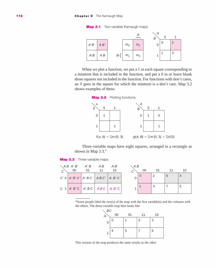
When we plot a function, we put a 1 in each square corresponding toa minterm that is included in the function, and put a 0 in or leave blankthose squares not included in the function. For functions with don’t cares,an X goes in the square for which the minterm is a don’t care. Map 3.2shows examples of these.
112 Chapter 3 The Karnaugh Map
Map 3.1 Two-variable Karnaugh maps.
A�B � A B �
A�B A B
0 2
1 3
0 1
0
1
A
B
m0 m2
m1B
A
m3
Map 3.2 Plotting functions.
1
1
1
0
0
1
ab
f (a, b) � �m (0, 3)
1 X
1
0 1
0
1
A
B
g(A, B) � �m (0, 3) � �d (2)
Map 3.3 Three-variable maps.
A �B �C � A� B C � A B C � A B �C �
A� B �C A� B C A B C A B �C
00 01 11 10A� B� A� B A B A B�
0
1
C�
C
A B
C0 2 6 4
1 3 7 5
00 01 11 10
0
1
A B
C
*Some people label the row(s) of the map with the first variable(s) and the columns withthe others. The three-variable map then looks like
This version of the map produces the same results as the other.
Three-variable maps have eight squares, arranged in a rectangle asshown in Map 3.3.*
0 1 3 2
4 5 7 6
00 01 11 10
0
1
B C
A
mar91647_c03a_111_128.qxd 11/5/08 11:46 AM Page 112

Notice that the last two columns are not in numeric order. That is the keyidea that makes the map work. By organizing the map that way, theminterms in adjacent squares can always be combined using the adja-cency property,
P9a. ab � ab� � a
m0 � m1: A�B�C� � A�B�C � A�B�
m4 � m6: AB�C� � ABC� � AC�
m7 � m5: ABC � AB�C � AC
Also, the outside columns (and the outside rows when there are four rows)are adjacent. Thus,
m0 � m4: A�B�C� � AB�C� � B�C�
m1 � m5: A�B�C � AB�C � B�C
If we had ordered the columns in numeric order, as shown in Map 3.4(where the algebraic version of the minterms is shown only for m2 andm4), we would not be able to combine adjacent squares:
3.1 Introduction to the Karnaugh Map 113
Map 3.4 Incorrect arrangement ofthe map.
0A� B C �
2A B � C �
4 6
1 3 5 7
00 01 10 11
0
1
A B
C
EXAMPLE 3.1
m2 � m4 � A�BC� � AB�C� � C�(A�B � AB�)
However, we cannot manipulate that into a single term.Product terms that correspond to the sum of two minterms appear
as two adjacent 1’s on the map. The terms of Example 3.1 are shown inMap 3.5.
It is sometimes more convenient to draw the map in a vertical orien-tation (that is, two columns and four rows) as shown in Map 3.6. Bothversions of the map produce the same results.
In reading the map, it is useful to label the pairs of columns (in thosearrangements where there are four columns) as shown in Map 3.7. Thus,1’s in squares 4 and 6 are in the A columns and the C� row (that is, not inthe C row), producing the AC� term as shown earlier.
mar91647_c03a_111_128.qxd 11/5/08 11:46 AM Page 113

114 Chapter 3 The Karnaugh Map
Map 3.5 Product terms corresponding to groups of two.
00 01 11 10
0 1
1
A B
A� B �
C
1
00 01 11 10
0 1 1
1
A B
A C �
C 00 01 11 10
0
1
A B
A C
C
1 1
00 01 11 10
0 1 1
1
A B
B � C �
C 00 01 11 10
0
1 1 1
A B
B � C
C
Map 3.6 Vertical orientation of three-variable map.
0 1
00 0 4
A
B C
01 1 5
11 3 7
10 2 6
0 1
00 1
A
B C
01 1
11
10
A� B �
0 1
00
A
B C
01
1
1
11
10
A C �
0 1
00
A
B C
01 1
111
10
A C
Map 3.7 Map with columnslabeled.
00 01 11 10
00 2 6 4
1 C
A B
C
1 3 7 5
B
A
The four-variable map consists of 16 squares in the 4 by 4 arrange-ment shown in Map 3.8.
As with the three-variable map, 1’s in two adjacent squares (wherethe top and bottom rows as well as the left and right columns are consid-ered to be adjacent) correspond to a single product term (combined usingP9a). Example 3.2 shows three such terms.
mar91647_c03a_111_128.qxd 11/5/08 11:46 AM Page 114

m13 � m9: ABC�D � AB�C�D � AC�D
m3 � m11: A�B�CD � AB�CD � B�CD
m0 � m2: A�B�C�D� � A�B�CD� � A�B�D�
3.1 Introduction to the Karnaugh Map 115
00 01 11 10
00
01
11
10
A B
A C �D
C D
1 1
00 01 11 10
00
01
11
10
A B
B �C D
C D
1 1
00 01 11 10
00
01
11
10
A B
A� B �D�
C D
1
1
Map 3.8 The four-variable map.
00 01 11 10
00
01
11 A�B C D A B C D A B�C D
A�B C D� A B C D�10
A B
C D00 01 11 10
00
01
11
0 4 12 8
1 5 13 9
3 7 15 11
2 6 14 1010
A B
C D
EXAMPLE 3.2
Up to this point, all of the product terms that we have shown corre-spond to two minterms combined using P9a. These correspond to aproduct term with one literal missing, that is, with only two literals in athree-variable function and three literals in a four-variable function. Letus next look at the maps of Map 3.9 with a group of four 1’s.
mar91647_c03a_111_128.qxd 11/5/08 11:46 AM Page 115

On the map to the left, we have circled two groups of two, one form-ing the term A�C and the other forming the term AC. Obviously, P9a canbe applied again to these two terms, producing
A�C � AC � C
116 Chapter 3 The Karnaugh Map
Map 3.9 A group of four 1’s.
00 01 11 10
0
1
A B
A� C A C
C
1 1 1 1
00 01 11 10
0
1
A B
C
C
1 1 1 1
That is shown on the map to the right as a rectangle of four 1’s. In gen-eral, rectangles of four 1’s will correspond to a product term with two ofthe variables missing (that is, a single literal for three-variable problemsand a two-literal term for four-variable problems).
We could have factored C from all of the terms producing
A�B�C � A�BC � ABC � AB�C � C(A�B� � A�B � AB � AB�)
However, the sum inside the parentheses is just a sum of all of theminterms of A and B; that must be 1. Thus, we can get the result in justthat one step. Indeed, we could have added a secondary property to P9,namely,
P9aa. a�b� � a�b � ab � ab� � 1P9bb. (a� � b�) (a� � b) (a � b) (a � b�) � 0
These can be proved by repeated application of P9, first to the first twoterms, then to the last two terms, and finally to the resulting terms asshown
(a�b� � a�b) � (ab � ab�) � (a�) � (a) � 1
[(a� � b�) (a� � b)][(a � b) (a � b�)] � [a�][a] � 0
Some examples of such groups for four-variable problems are shown inMap 3.10.
The easiest way to identify the term from the map is by determiningin which row(s) and column(s) all of the 1’s are located. Thus, on the firstmap, the 1’s in the group on the left are all in the 00 (A�B�) column andthus the term is A�B�. The other group has its 1’s in the 11 and 10columns; the common feature is the 1 in the A position (which corre-sponds to A). Furthermore, the 1’s are in the 01 and 11 rows; there is acommon 1 in the D position. Thus, the term is AD. In the middle map, the
mar91647_c03a_111_128.qxd 11/5/08 11:46 AM Page 116

1’s are in the 00 and 10 columns, producing B� and the 01 and 11 rows,resulting in D; the term is thus B�D. (Notice, by the way, that that termalso appears on the first map, even though it was not circled.) On the lastmap, the four corners produce the term B�D� (since all the 1’s are in the00 or 10 columns and the 00 or 10 rows). The middle group is BD. Anyof these terms could also be obtained algebraically by first writing theminterms, then applying P10a to pairs of terms, and then applying itagain to the two terms that resulted (as we did for the three-variableexample). However, the whole idea of the map is to eliminate the need todo algebra.
Two adjacent groups of four can be combined in a similar way toform a group of eight squares (with three of the literals missing). Twosuch groups are shown in Map 3.11. The terms are A� for the map on theleft and D� for the map on the right.
3.1 Introduction to the Karnaugh Map 117
Map 3.10 Examples of groups of four.
00 01 11 10
00
01
11
10
A B
A� B � A D
C D
11 1
1
11 1
1
00 01 11 10
00
01
11
10
A B
B �D
C D
1 1
1 1
00 01 11 10
00
01
11
10
A B
B �D � B D
C D
11
1
11
1
1
1
Map 3.11 Groups of eight.
00 01 11 10
00
01
11
10
A B
C D
1
1
1
1
1
1
1
1
00 01 11 10
00
01
11
10
A B
C D
1
1
1 1 1
1 1 1
mar91647_c03a_111_128.qxd 11/5/08 11:46 AM Page 117
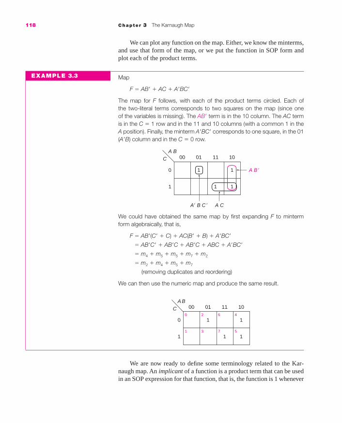
We can plot any function on the map. Either, we know the minterms,and use that form of the map, or we put the function in SOP form andplot each of the product terms.
Map
F � AB� � AC � A�BC�
The map for F follows, with each of the product terms circled. Each ofthe two-literal terms corresponds to two squares on the map (since oneof the variables is missing). The AB� term is in the 10 column. The AC termis in the C � 1 row and in the 11 and 10 columns (with a common 1 in theA position). Finally, the minterm A�BC� corresponds to one square, in the 01(A�B) column and in the C � 0 row.
118 Chapter 3 The Karnaugh Map
EXAMPLE 3.3
00 01 11 10
0
1
A B
A B �
A� B C � A C
C
1
1 1
1
We could have obtained the same map by first expanding F to mintermform algebraically, that is,
F � AB�(C� � C) � AC(B� � B) � A�BC�
� AB�C� � AB�C � AB�C � ABC � A�BC�
� m4 � m5 � m5 � m7 � m2
� m2 � m4 � m5 � m7
(removing duplicates and reordering)
We can then use the numeric map and produce the same result.
000 2 6 4
1 3 7 5
01 11 10
0
1
A B
C
1
1 1
1
We are now ready to define some terminology related to the Kar-naugh map. An implicant of a function is a product term that can be usedin an SOP expression for that function, that is, the function is 1 whenever
mar91647_c03a_111_128.qxd 11/5/08 11:46 AM Page 118

the implicant is 1 (and maybe other times, as well). From the point ofview of the map, an implicant is a rectangle of 1, 2, 4, 8, . . . (any powerof 2) 1’s.* That rectangle may not include any 0’s. All minterms areimplicants.
Consider the function, F, of Map 3.12. The second map shows thefirst four groups of 2; the third map shows the other groups of 2 and thegroup of 4.
3.1 Introduction to the Karnaugh Map 119
Map 3.12 A function to illustrate definitions.
00 01 11 10
00
01
11
10
A B
C D
1 1
11 1 1
1
00 01 11 10
00
01
11
10
A B
C D
1 1
11 1 1
1
00 01 11 10
00
01
11
10
A B
C D
1 1
11 1 1
1
The implicants of F are
Minterms Groups of 2 Groups of 4A�B�C�D� A�CD CD
A�B�CD BCD
A�BCD ACD
ABC�D� B�CD
ABC�D ABC�
ABCD ABD
AB�CD
Any SOP expression for F must be a sum of implicants. Indeed, wemust choose enough implicants such that each of the 1’s of F areincluded in at least one of these implicants. Such an SOP expressionis sometimes referred to as a cover of F, and we sometimes say thatan implicant covers certain minterms (for example, ACD covers m11
and m15).Implicants must be rectangular in shape and the number of 1’s in the
rectangle must be a power of 2. Thus, neither of the functions whosemaps are shown in Example 3.4 are covered by a single implicant, butrather by the sum of two implicants each (in their simplest form).
*We will expand the definition of an implicant to include maps with don’t cares in Section 3.3.
mar91647_c03a_111_128.qxd 11/5/08 11:46 AM Page 119

EXAMPLE 3.4
00 01 11
G
10
00
01
11
10
A B
C D
1
1
1
00 01 11 10
00
01
11
10
A B
C D
1
1
11
H
A prime implicant is an implicant that (from the point of view of themap) is not fully contained in any one other implicant. For example, it isa rectangle of two 1’s that is not part of a single rectangle of four 1’s. OnMap 3.13, all of the prime implicants of F are circled. They areA�B�C�D�, ABC�, ABD, and CD. Note that the only minterm that is notpart of a larger group is m0 and that the other four implicants that aregroups of two 1’s are all part of the group of four.
From an algebraic point of view, a prime implicant is an implicantsuch that if any literal is removed from that term, it is no longer an impli-cant. From that viewpoint, A�B�C�D� is a prime implicant because B�C�D�,A�C�D�, A�B�D�, and A�B�C� are not implicants (that is, if we remove anyliteral from that term, we get a term that is 1 for some input combinationsfor which the function is to be 0). However, ACD is not a prime implicantsince when we remove A, leaving CD, we still have an implicant. (Surely,the graphical approach of determining which implicants are prime impli-cants is easier than the algebraic method of attempting to delete literals.)
The purpose of the map is to help us find minimum SOP expres-sions, where we defined minimum as being minimum number of productterms (implicants), and among those with the same number of impli-cants, the ones with the fewest number of literals. However, the onlyproduct terms that we need consider are prime implicants. Why? Say wefound an implicant that was not a prime implicant. Then, it must be con-tained in some larger implicant, a prime implicant. But that larger impli-cant (say four 1’s rather than two) has fewer literals. That alone makes a
Map 3.13 Prime implicants.
00 01 11 10
00
01
11
10
A B
C D
1 1
11 1 1
1
G consists of three minterms, ABC�D, ABCD, and ABCD�, in the shape of arectangle. It can be reduced no further than is shown on the map, namely,to ABC � ABD, since it is a group of three 1’s, not two or four. Similarly, Hhas the same three minterms plus A�BC�D; it is a group of four, but not inthe shape of a rectangle. The minimum expression is, as shown on themap, BC�D � ABC. (Note that ABD is also an implicant of G, but it includes1’s that are already included in the other terms.)
120 Chapter 3 The Karnaugh Map
mar91647_c03a_111_128.qxd 11/5/08 11:46 AM Page 120

[SP 1; EX 1]
3.2 Minimum Sum of Product Expressions Using the Karnaugh Map 121
solution using the term that is not a prime implicant not a minimum. (Forexample, CD has two literals, whereas, ACD has three.) Furthermore,that larger implicant covers more 1’s, which often will mean that weneed fewer terms.
An essential prime implicant is a prime implicant that includes atleast one 1 that is not included in any other prime implicant. (If we wereto circle all of the prime implicants of a function, the essential primeimplicants are those that circle at least one 1 that no other prime implicantcircles.) In the example of Map 3.13, A�B�C�D�, ABC�, and CD areessential prime implicants; ABD is not. The term essential is derived fromthe idea that we must use that prime implicant in any minimum SOPexpression. A word of caution is in order. There will often be a prime implicant that is used in a minimum solution (even in all minimum solu-tions when more than one equally good solution exists) that is not “essen-tial.” That happens when each of the 1’s covered by this prime implicantcould be covered in other ways. We will see examples of that in Section 3.2.
3.2 MINIMUM SUM OF PRODUCTEXPRESSIONS USING THE KARNAUGH MAP
In this section, we will describe two methods for finding minimum SOPexpressions using the Karnaugh map. Although these methods involvesome heuristics, we can all but guarantee that they will lead to a mini-mum SOP expression (or more than one when multiple solutions exist)for three- and four-variable problems. (It also works for five- and six-variable maps, but our visualization in three dimensions is more limited.We will discuss this in detail in Section 3.6.)
In the process of finding prime implicants, we will be consideringeach of the 1’s on the map starting with the most isolated 1’s. By iso-lated, we mean that there are few (or no) adjacent squares with a 1 in it.In an n-variable map, each square has n adjacent squares. Examples forthree- and four-variable maps are shown in Map 3.14.
Map 3.14 Adjacencies on three- and four-variable maps.
1
1
1
1
mar91647_c03a_111_128.qxd 11/5/08 12:49 PM Page 121

Map Method 11. Find all essential prime implicants. Circle them on the map and
mark the minterm(s) that make them essential with a star (★). Dothis by examining each 1 on the map that has not already beencircled. It is usually quickest to start with the most isolated 1’s, thatis, those that have the fewest adjacent squares with 1’s in them.
2. Find enough other prime implicants to cover the function. Do thisusing two criteria:a. Choose a prime implicant that covers as many new 1’s (that is,
those not already covered by a chosen prime implicant).b. Avoid leaving isolated uncovered 1’s.
It is often obvious what “enough” is. For example, if there are fiveuncovered 1’s and no prime implicants cover more than two of them,then we need at least three more terms. Sometimes, three may not besufficient, but it usually is.
We will now look at a number of examples to demonstrate this method. First, we will look at the example used to illustrate thedefinitions.
As noted, m0 has no adjacent 1’s; therefore, it (A�B�C�D�) is a prime impli-cant. Indeed, it is an essential prime implicant, since no other prime implicantcovers this 1. (That is always the case when minterms are prime implicants.)The next place that we look is m12, since it has only one adjacent 1. Those1’s are covered by prime implicant ABC�. Indeed, no other prime implicantcovers m12, and thus ABC� is essential. (Whenever we have a 1 with onlyone adjacent 1, that group of two is an essential prime implicant.) At thispoint, the map has become
and
F � A�B�C�D� � ABC� � � � �
00 01 11 10
00
01
11
10
A B
C D
1★ 1★
11 1 1
1
122 Chapter 3 The Karnaugh Map
EXAMPLE 3.5
mar91647_c03a_111_128.qxd 11/5/08 11:46 AM Page 122

Each of the 1’s that have not yet been covered are part of the group of four,CD. Each has two adjacent squares with 1’s that are part of that group. Thatwill always be the case for a group of four. (Some squares, such as m15 mayhave more than two adjacent 1’s.) CD is essential because no other primeimplicant covers m3, m7, or m11. However, once that group is circled, wehave covered the function:
resulting in
F � A�B�C�D � ABC� � CD
In this example, once we have found the essential prime implicants, we aredone; all of the 1’s have been covered by one (or more) of the essentialprime implicants. We do not need step 2. There may be other prime impli-cants that were not used (such as ABD in this example).
We start looking at the most isolated 1, m11. It is covered only by the groupof two shown, wyz. The other essential prime implicant is y�z� because ofm0, m8, or m12. None of these are covered by any other prime implicant;each makes that prime implicant essential. The second map shows thesetwo terms circled.
00 01 11 10
00
01
11
10
w x
y z
1★ 1 1★ 1★
1 1 1★
1
00 01 11 10
00
01
11
10
w x
y z
1 1 11
1 1 1
1
00 01 11 10
00
01
11
10
A B
C D
1★ 1★
1★1★ 1 1★
1
3.2 Minimum Sum of Product Expressions Using the Karnaugh Map 123
EXAMPLE 3.6
mar91647_c03a_111_128.qxd 11/5/08 11:46 AM Page 123

That leaves two 1’s uncovered. Each of these can be covered by two differ-ent prime implicants, but the only way to cover them both with one term isshown on the first of the maps below.
Thus, the minimum sum of product solution is
f � y�z� � wyz � w�xz
The other two prime implicants are w�xy� and xyz, circled in brown on thelast map. They are redundant, however, since they cover no new 1’s. Eventhough w�xz must be used in a minimum solution, it does not meet the def-inition of an essential prime implicant; each of the 1’s covered by it can becovered by other prime implicants.
We will next look at the “dead end” example from Chapter 2(Example 2.2).
f � a�b�c� � a�bc� � a�bc � ab�c�
In the first attempt at algebraic manipulation, we grouped the first twominterms. But, as can be seen on the left-hand map below, the two 1’s thatare left could not be combined and resulted in a three-term solution. Further-more, a�c� is not an essential prime implicant. If, on the other hand, we usedthe map, we could see that choosing the two essential prime implicants onthe right-hand map includes all of the minterms and produces the solution
f � a�b � b�c�
00 01 11 10
0
1
a b
c
1
11 1
00 01 11 10
0
1
a b
c
1★
11 1★
00 01 11 10
00
01
11
10
w x
y z
1★ 1 1★ 1★
1 1 1★
1
00 01 11 10
00
01
11
10
w x
y z
1★ 1 1★ 1★
1 1 1★
1
124 Chapter 3 The Karnaugh Map
EXAMPLE 3.7
mar91647_c03a_111_128.qxd 11/5/08 11:46 AM Page 124

Sometimes, after selecting all of the essential prime implicants,there are two choices for covering the remaining 1’s, but only one ofthese produces a minimum solution, as in Example 3.8.
f (a, b, c, d) � �m(0, 2, 4, 6, 7, 8, 9, 11, 12, 14)
The first map shows the function and the second shows all essential primeimplicants circled. In each case, one of the 1’s (as indicated with a star, ★)can be covered by only that prime implicant. (That is obvious from the lastmap, where the remaining two prime implicants are circled.)
3.2 Minimum Sum of Product Expressions Using the Karnaugh Map 125
EXAMPLE 3.8
00 01 11 10
00
01
11
10
a b
c d
1 1 1 1
1 1 1
1 1
1
00 01 11 10
00
01
11
10
a b
c d
1 1 1 1
1★ 1 1★
1★ 1★
1
00 01 11 10
00
01
11
10
a b
c d
1 1 1 1
1 1 1
1 1
1
Only one 1 (m8) is not covered by an essential prime implicant. It can becovered in two ways, by a group of four (in brown) and a group of two(tan). Clearly, the group of four provides a solution with one less literal,namely,
f � a�d� � bd� � a�bc � ab�d � c�d�
When asking whether a 1 makes a group of four an essential primeimplicant on a four-variable map, we need find only two adjacent 0’s. Ifthere are fewer than two adjacent 0’s, this 1 must be either in a group ofeight or part of two or more smaller groups. Note that in Example 3.8, m2
and m14 have two adjacent 0’s, and thus each makes a prime implicantessential. In contrast, m0, m4, m8, and m12 each have only one adjacent 0and are each covered by two or three prime implicants.
We will now consider some examples with multiple minimum solu-tions, starting with the three-variable function used to illustrate the defi-nition of terminology in Section 2.2.3.
mar91647_c03a_111_128.qxd 11/5/08 11:46 AM Page 125

x�yz� � x�yz � xy�z� � xy�z � xyz
A map of that function is shown on the left. The two essential prime impli-cants are shown on the map on the right.
After finding the two essential prime implicants, m7 is still uncovered. Thefollowing maps show the two solutions.
This example is one we call “don’t be greedy.”
At first glance, one might want to take the only group of four (circled in tan).However, that term is not an essential prime implicant, as is obvious oncewe circle all of the essential prime implicants and find that the four 1’s in thecenter are covered. Thus, the minimum solution is
G � A�BC� � A�CD � ABC � AC�D
00 01 11 10
00
01
11
10
A BC D
1
1
11 1
111
00 01 11 10
00
01
11
10
A BC D
1★
1★
1 11★
1★11
00 01 11 10
0
1
x y
x� y � x y � � x z
z
1 1
1
1
1
x� y � x y � � y z
00 01 11 10
0
1
x y
z
1 1
1
1
1
00 01 11 10
0
1
x y
z
1 1
1
1
1
00 01 11 10
0
1
x y
z
1 1 1
1★1★
126 Chapter 3 The Karnaugh Map
EXAMPLE 3.9
EXAMPLE 3.10
mar91647_c03a_111_128.qxd 11/5/08 12:49 PM Page 126

g(w, x, y, z) � �m(2, 5, 6, 7, 9, 10, 11, 13, 15)
The function is mapped first, and the two essential prime implicants areshown on the second map, giving
g � xz � wz � � � �
Although m2 looks rather isolated, it can indeed be covered by w�yz� (withm6) or by x�yz� (with m10). After choosing the essential prime implicants, theremaining three 1’s can each be covered by two different prime implicants.Since three 1’s still need to be covered (after choosing the essential primeimplicants), and since all the remaining prime implicants are groups of twoand thus have three literals, we need at least two more of these primeimplicants. Indeed, there are three ways to cover the remaining 1’s with twomore prime implicants. Using the first criteria, we choose one of the primeimplicants that covers two new 1’s, w�yz�, as shown on the left-hand map.
00 01 11 10
00
01
11
10
w x
y z
1 1 1
1 1 1
111
00 01 11 10
00
01
11
10
w x
y z
1 1 1
1 1 1
1★11★
3.2 Minimum Sum of Product Expressions Using the Karnaugh Map 127
00 01 11 10
00
01
11
10
w x
y z
1 1 1
1 1 1
111
00 01 11 10
00
01
11
10
w x
y z
1 1 1
1 1 1
111
00 01 11 10
00
01
11
10
w x
y z
1 1 1
1 1 1
111
EXAMPLE 3.11
Then, only m10 remains, and it can be covered either by wx�y or by x�yz�, asshown on the center map. Similarly, we could have started with x�yz�, inwhich case we could use w�xy to complete the cover, as on the right-handmap. (We could also have chosen w�yz�, but that repeats one of the answers from before.) Thus, the three solutions are
mar91647_c03a_111_128.qxd 11/5/08 11:46 AM Page 127

g � xz � wz � w�yz� � wx�y
g � xz � wz � w�yz� � x�yz�
g � xz � wz � x�yz� � w�xy
All three minimum solutions require four terms and 10 literals.
At this point, it is worth stating the obvious.
128 Chapter 3 The Karnaugh Map
EXAMPLE 3.12
00 01 11 10
00
01
11
10
A B
C D
1 11
1 11
11 1
11
00 01 11 10
00
01
11
10
A B
C D
1★ 11
1★1 1
1 11★
1★ 1
00 01 11 10
00
01
11
10
A B
C D
1 11
11 1
1 11
1 1
The four essential prime implicants are shown on the second map, leavingthree 1’s to be covered:
F � A�C�D� � AC�D � A�CD � ACD� � � � �
These squares are shaded on the right-hand map. The three other primeimplicants, all groups of four, are also shown on the right-hand map. Eachof these covers two of the remaining three 1’s (no two the same). Thus, anytwo of B�D�, AB�, and B�C can be used to complete the minimum SOPexpression. The resulting three equally good answers are
F � A�C�D� � AC�D � A�CD � ACD� � B�D� � AB�
F � A�C�D� � AC�D � A�CD � ACD� � B�D� � B�C
F � A�C�D� � AC�D � A�CD � ACD� � AB� � B�C
COMMON MISTAKE: If there are multiple solutions, all minimumsolutions must have the same number of terms and literals. If, forexample, you find a minimum solution with three terms and sevenliterals, no solution with four terms is minimum, and no solutionwith three terms and eight literals is minimum.
mar91647_c03a_111_128.qxd 11/5/08 11:46 AM Page 128

3.2 Minimum Sum of Product Expressions Using the Karnaugh Map 129
EXAMPLE 3.13
Once again there are two essential prime implicants, as shown on the right-hand map. The most isolated 1’s are m10 and m15. Each has only two adja-cent 1’s. But all of the 1’s in groups of four have at least two adjacent 1’s; ifthere are only two, then that minterm will make the prime implicant essen-tial. (Each of the other 1’s in those groups of four has at least three adjacent1’s.) The essential prime implicants give us
f � b�d� � bd � � � �
There are three 1’s not covered by the essential prime implicants. There isno single term that will cover all of them. However, the two in the 01 col-umn can be covered by either of two groups of four, as shown on the mapon the left (a�d� circled in brown, a�b in tan). And, there are two groups oftwo that cover m9 (ac�d circled in brown, ab�c� in tan), shown on the mapto the right.
We can choose one term from the first pair and (independently) one fromthe second pair. Thus, there are four solutions. We can write the solution asshown, where we take one term from within each bracket
f � b�d� � bd � � � � � �ac�dab�c�
a�d�
a�b
00 01 11 10
00
01
11
10
a b
c d
1 1 1★
1 1 1
1 1★
111
00 01 11 10
00
01
11
10
a b
c d
1 1 1★
1 1 1
1 1★
111
00 01 11 10
00
01
11
10
a b
c d
1 1 1
1 1 1
1 1
111
00 01 11 10
00
01
11
10
a b
c d
1 1 1★
1 1 1
1 1★
111
mar91647_c03b_129_161.qxd 11/5/08 11:47 AM Page 129

or we can write out all four expressions
f � b�d� � bd � a�d� � ac�d
� b�d� � bd � a�d� � ab�c�
� b�d� � bd � a�b � ac�d
� b�d� � bd � a�b � ab�c�
130 Chapter 3 The Karnaugh Map
00 01 11 10
00
01
11
10
A B
C D
1 11
1 11
11 1
11
00 01 11 10
00
01
11
10
A B
C D
1★ 11
1★1 1
1 11★
1★ 1
00 01 11 10
00
01
11
10
A B
C D
1 11
11 1
1 11
1 1
EXAMPLE 3.14
The four essential prime implicants are shown on the second map, leavingthree 1’s to be covered:
F � A�C�D� � AC�D � A�CD � ACD� � � � �
These squares are shaded on the third map. The three other prime impli-cants, all groups of four, are also shown on the third map. Each of thesecovers two of the remaining three 1’s (no two the same). Thus any two ofB�D�, AB�, and B�C can be used to complete the minimum sum of productsexpression. The resulting three equally good answers are
F � A�C�D� � AC�D � A�CD � ACD� � B�D� � AB�
F � A�C�D� � AC�D � A�CD � ACD� � B�D� � B�C
F � A�C�D� � AC�D � A�CD � ACD� � AB� � B�C
Before doing additional (more complex) examples, we will intro-duce a somewhat different method for finding minimum sum of productsexpressions.
Map Method 21. Circle all of the prime implicants.
2. Select all essential prime implicants; they are easily identified byfinding 1’s that have only been circled once.
3. Then choose enough of the other prime implicants (as inMethod 1). Of course, these prime implicants have already beenidentified in step 1.
mar91647_c03b_129_161.qxd 11/5/08 11:47 AM Page 130

3.2 Minimum Sum of Product Expressions Using the Karnaugh Map 131
EXAMPLE 3.15
00 01 11 10
00
01
11
10
A B
C D
1 11
11
11
1111
00 01 11 10
00
01
11
10
A B
C D
1 11
1 1
1★ 1
11★1 1
00 01 11 10
00
01
11
10
A B
C D
1 11
1 1
1 1
111 1
All of the prime implicants have been circled on the center map. Note thatm0 has been circled three times and that several minterms have beencircled twice. However, m3 and m5 have only been circled once. Thus, theprime implicants that cover them, A�B� and C�D are essential. On the thirdmap, we have shaded the part of the map covered by essential primeimplicants to highlight what remains to be covered. There are four 1’s, eachof which can be covered in two different ways, and five prime implicants notused yet. No prime implicant covers more than two new 1’s; thus, we needat least two more terms. Of the groups of four, only B�D� covers two new1’s; B�C� covers only one. Having chosen the first group, we must use ABCto cover the rest of the function, producing
F � A�B� � C�D � B�D� � ABC
Notice that this is the only set of four prime implicants (regardless of size)that covers the function.
00 01 11 10
00
01
11
10
W X
Y Z
1 11
1 1★ 1 1
11
00 01 11 10
00
01
11
10
W X
Y Z
1 11
1 1 1 1
11
00 01 11 10
00
01
11
10
W X
Y Z
1 11
1 1 1 1
11
G(A, B, C, D) � �m(0, 1, 3, 7, 8, 11, 12, 13, 15)
This is a case with more 1’s left uncovered after finding the essential primeimplicant. The first map shows all the prime implicants circled. The only essential prime implicant is YZ; there are five 1’s remaining to be covered.Since all of the other prime implicants are groups of two, we need threemore prime implicants. These 1’s are organized in a chain, with each primeimplicant linked to one on either side. If we are looking for just one solution,we should follow the guidelines from Method 1, choosing two terms that
EXAMPLE 3.16
mar91647_c03b_129_161.qxd 11/5/08 11:47 AM Page 131

each cover new 1’s and then select a term to cover the remaining 1. Onesuch example is shown on the third map, starting with WXY� and X�Y�Z�. Ifwe wish to find all of the minimum solutions, one approach is to start at oneend of the chain (as shown in the second map). (We could have started atthe other end, with m13, and achieved the same results.) To cover m1, wemust either use W�X�Z, as shown in brown above, or W�X�Y� (as shown onthe maps below). Once we have chosen W�X�Z, we have no more freedom,since the terms shown on the third map above are the only way to cover theremaining 1’s in two additional terms. Thus, one solution is
F � YZ � W�X�Z � X�Y�Z� � WXY�
The next three maps show the solutions using W�X�Y� to cover m0.
132 Chapter 3 The Karnaugh Map
EXAMPLE 3.17
00 01 11 10
00
01
11
10
a b
c d
1 1
1 1
1 1
11
00 01 11 10
00
01
11
10
a b
c d
1 1
1 1
1 1
11
00 01 11 10
00
01
11
10
a b
c d
1 1
1 1
1 1
11
00 01 11 10
00
01
11
10
W X
Y Z
1 11
1 1 1 1
11
00 01 11 10
00
01
11
10
W X
Y Z
1 11
1 1 1 1
11
00 01 11 10
00
01
11
10
W X
Y Z
1 11
1 1 1 1
11
After choosing W�X�Y�, there are now three 1’s to be covered. We can usethe same last two terms as before (left) or use WY�Z� to cover m8 (right twomaps). The other three solutions are thus
F � YZ � W�X�Y� � X�Y�Z� � WXY�
F � YZ � W�X�Y� � WY�Z� � WXY�
F � YZ � W�X�Y� � WY�Z� � WXZ
We will now look at some examples with no essential prime impli-cants. A classic example of such a function is shown in Example 3.17.
mar91647_c03b_129_161.qxd 11/5/08 11:47 AM Page 132

3.2 Minimum Sum of Product Expressions Using the Karnaugh Map 133
There are eight 1’s; all prime implicants are groups of two. Thus, we need atleast four terms in a minimum solution. There is no obvious place to start;thus, in the second map, we arbitrarily chose one of the terms, a�c�d�.Following the guidelines of step 2, we should then choose a second termthat covers two new 1’s, in such a way as not to leave an isolated uncov-ered 1. One such term is bc�d, as shown on the third map. Another possi-bility would be b�cd� (the group in the last row). As we will see, that groupwill also be used. Repeating that procedure, we get the cover on the left-hand map below,
f � a�c�d� � bc�d � acd � b�cd�
Notice that if, after starting with a�c�d�, we chose one of the primeimplicants not included in this solution above, such as abd, shown on themiddle map, we leave an isolated uncovered 1 (which would require a thirdterm) plus three more 1’s (which would require two more terms). A solutionusing those two terms would require five terms (obviously not minimumsince we found one with four). Another choice would be a term such asa�b�d�, which covers only one new 1, leaving five 1’s uncovered. That, too,would require at least five terms.
The other solution to this problem starts with a�b�d�, the only otherprime implicant to cover m0. Using the same process, we obtain the map onthe right and the expression
f � a�b�d� � a�bc� � abd � ab�c
G(A, B, C, D) � �m(0, 1, 3, 4, 6, 7, 8, 9, 11, 12, 13, 14, 15)
All of the prime implicants are groups of four. Since there are 13 1’s, weneed at least four terms. The first map shows all of the prime implicantscircled; there are nine. There are no 1’s circled only once, and thus, thereare no essential prime implicants.
00 01 11 10
00
01
11
10
a b
c d
1 1
1 1
1 1
11
00 01 11 10
00
01
11
10
a b
c d
1 1
1 1
1 1
11
00 01 11 10
00
01
11
10
a b
c d
1 1
1 1
1 1
11
EXAMPLE 3.18
mar91647_c03b_129_161.qxd 11/5/08 11:47 AM Page 133

134 Chapter 3 The Karnaugh Map
As a starting point, we choose one of the minterms covered by onlytwo prime implicants, say m0. On the second map, we used C�D� to coverit. Next, we found two additional prime implicants that cover four new 1’seach, as shown on the third map. That leaves just m13 to be covered. As canbe seen on the fourth map (shown below), there are three different primeimplicants that can be used. Now, we have three of the minimum solutions.
F � C�D� � B�D � BC � �AB or AC� or AD�
If, instead of using C�D� to cover m0, we use B�C� (the only other primeimplicant that covers m0), as shown on the next map, we can find two othergroups of four that each cover four new 1’s and leave just m13 to becovered. Once again, we have three different ways to complete the cover(the same three terms as before).
Thus, there are six equally good solutions
F � � � � � �where one group of terms is chosen from the first bracket and an additionalterm from the second. We are sure that there are no better solutions, sinceeach uses the minimum number of prime implicants, four. Although it maynot be obvious without trying other combinations, there are no additionalminimum solutions.
ABAC�
AD
C�D� � B�D � BCB�C� � BD� � CD
00 01 11 10
00
01
11
10
A B
C D
1 1 1 1
1 1
111 1
1 11
00 01 11 10
00
01
11
10
A B
C D
1 1 1 1
1 1
111 1
1 11
00 01 11 10
00
01
11
10
A B
C D
1 1 1 1
1 1
111 1
1 11
00 01 11 10
00
01
11
10
A B
C D
1 1 1 1
1 1
111 1
1 11
00 01 11 10
00
01
11
10
A B
C D
1 1 1 1
1 1
111 1
1 11
00 01 11 10
00
01
11
10
A B
C D
1 1 1 1
1 1
111 1
1 11
mar91647_c03b_129_161.qxd 11/5/08 11:47 AM Page 134

3.3 Don’t Cares 135
EXAMPLE 3.19
00 01 11 10
00
01
11
10
a b
c d
1★ 1
1 1 1
11 1
1 11
00 01 11 10
00
01
11
10
a b
c d
1 1
1 1 1
11 1
1 11
00 01 11 10
00
01
11
10
a b
c d
1 1
1 1 1
11 1
1 11
This function has one essential prime implicant (a minterm) and ten other1’s. All of the other prime implicants are groups of two. The second mapshows all 13 prime implicants. The prime implicants of this function are
a�b�c�d a�cd b�cd ac�d bc�d bcd� acd�
a�cd a�bd abc� abd� ab�c ab�d
Note that every 1 (other than m0) can be covered by two or three differentterms.
Since there are ten 1’s to be covered by groups of two, we know thatwe need at least five terms, in addition to a�b�c�d�. The third map shows thebeginnings of an attempt to cover the function. Each term covers two new1’s without leaving any isolated uncovered 1. (The 1 at the top could becombined with m14.) The four 1’s that are left require three additional terms.After trying several other groupings, we can see that it is not possible tocover this function with less than seven terms. There are 32 different mini-mum solutions to this problem. A few of the solutions are listed below. Theremainder are left as an exercise (Exercise 1p).
f � a�b�c�d� � a�cd � bc�d � ab�d � abc� � a�bc � acd�
� a�b�c�d� � a�cd � bc�d � ab�d � abd� � bcd� � ab�c
� a�b�c�d� � b�cd � a�bd � ac�d � abd� � acd� � bcd�
� a�b�c�d� � b�cd � abc� � bcd� � a�bd � ab�c � ab�d
3.3 DON’T CARES
Finding minimum solutions for functions with don’t cares does notsignificantly change the methods we developed in the last section. Weneed to modify slightly the definitions of an implicant and a prime implicant, and clarify the definition of an essential prime implicant.
[SP 2, 3, 4; EX 2, 3, 4]
A number of other examples are included in Solved Problems 1 and2. Example 3.19 is one of the most complex four-variable problems,requiring more terms than we might estimate at first.
mar91647_c03b_129_161.qxd 11/5/08 11:47 AM Page 135

An implicant is a rectangle of 1, 2, 4, 8, . . . 1’s or X’s (containingno 0’s).
A prime implicant is an implicant not included in any one larger rec-tangle. Thus, from the point of view of finding prime implicants, X’s(don’t cares) are treated as 1’s.
An essential prime implicant is a prime implicant that covers at leastone 1 not covered by any other prime implicant (as always). Don’tcares (X’s) do not make a prime implicant essential.
Now, we just apply either of the methods of the last section. When we aredone, some of the X’s may be included and some may not. But we don’tcare whether or not they are included in the function.
F(A, B, C, D) � �m(1, 7, 10, 11, 13) � �d(5, 8, 15)
136 Chapter 3 The Karnaugh Map
EXAMPLE 3.20
00 01 11 10
00
01
11
10
A B
C D
X
1
1 X
1
1
1X
00 01 11 10
00
01
11
10
A B
C D
X
1
1★ X
1★
1
1★X
00 01 11 10
00
01
11
10
A B
C D
X
1
1 X
1
1
1X
We first mapped the function, entering a 1 for those minterms included inthe function and an X for the don’t cares. We found two essential primeimplicants, as shown on the center map. In each case, the 1’s with a starcannot be covered by any other prime implicant. That left the two 1’s circledin brown to cover the rest of the function. That is not an essential prime implicant, since each of the 1’s could be covered by another prime implicant(as shown in tan on the third map). However, if we did not use AB�C, wewould need two additional terms, instead of one. Thus, the only minimumsolution is
F � BD � A�C�D � AB�C
and terms AB�D� and ACD are prime implicants not used in the minimumsolution. Note that if all of the don’t cares were made 1’s, we would need afourth term to cover m8, making
F � BD � A�C�D � AB�C � AB�D� or
F � BD � A�C�D � ACD � AB�D�
and that if all of the don’t cares were 0’s, the function would become
F � A�B�C�D � A�BCD � ABC�D � AB�C
In either case, the solution is much more complex then when we treatedthose terms as don’t cares (and made two of them 1’s and the other a 0).
mar91647_c03b_129_161.qxd 11/5/08 11:47 AM Page 136

3.3 Don’t Cares 137
EXAMPLE 3.21
00 01 11 10
00
01
11
10
w x
y z
1
X
X
X
X
1
1
11
1
00 01 11 10
00
01
11
10
w x
y z
1★
X
X
X
X
1★
1
11
1
00 01 11 10
00
01
11
10
w x
y z
1
X
X
X
X
1
1
11
1
There are two essential prime implicants, as shown on the center map, x�zand w�yz. The group of four don’t cares, w�x�, is a prime implicant (since itis a rectangle of four 1’s or X’s) but it is not essential (since it does not coverany 1’s not covered by some other prime implicant). Surely, a prime impli-cant made up of all don’t cares would never be used, since that would adda term to the sum without covering any additional 1’s. The three remaining1’s require two groups of two and thus there are three equally good solu-tions, each using four terms and 11 literals:
g1 � x�z � w�yz � w�y�z� � wxy�
g2 � x�z � w�yz � xy�z� � wxy�
g3 � x�z � w�yz � xy�z� � wy�z
An important thing to note about Example 3.21 is that the threealgebraic expressions are not all equal. The first treats the don’t care form0 as a 1, whereas the other two (which are equal to each other) treat itas a 0. This will often happen with don’t cares. They must treat the spec-ified part of the function (the 1’s and the 0’s) the same, but the don’tcares may take on different values in the various solutions. The maps ofMap 3.15 show the three functions.
Map 3.15 The different solutions for Example 3.21.
00 01 11 10
00
01
11
10
w x
y z
1★
1
1
g1
1
1★
1
11
1
g2
00 01 11 10
00
01
11
10
w x
y z
1★
1
1 1★
1
11
1
g3
00 01 11 10
00
01
11
10
w x
y z
1★
1
1 1★
1
11
1
mar91647_c03b_129_161.qxd 11/5/08 11:47 AM Page 137

On the first map, we have shown the only essential prime implicant, c�d�,and the other group of four that is used in all three solutions, ab. (This mustbe used since the only other prime implicant that would cover m15 is bcd,which requires one more literal and does not cover any 1’s that are notcovered by ab.) The three remaining 1’s require two terms, one of whichmust be a group of two (to cover m3) and the other must be one of thegroups of four that cover m10. On the second map, we have shown two ofthe solutions, those that utilize b�d� as the group of four. On the third map,we have shown the third solution, utilizing ad�. Thus, we have
g1 � c�d� � ab � b�d� � a�cd
g2 � c�d� � ab � b�d� � a�b�c
g3 � c�d� � ab � ad� � a�b�c
We can now ask if these solutions are equal to each other. We can either map all three solutions as we did for Example 3.21, or we can makea table of the behavior of the don’t cares—one column for each don’t careand one row for each solution.
138 Chapter 3 The Karnaugh Map
EXAMPLE 3.22
00 01 11 10
00
01
11
10
a b
c d
1 1★ 1 1
1 1 1
X1 1
1 X
00 01 11 10
00
01
11
10
a b
c d
1 1 1 1
1 1 1
X1 1
1 X
00 01 11 10
00
01
11
10
a b
c d
1 1 1 1
1 1 1
X1 1
1 X
From the table, it is clear that g2 � g3, but neither is equal to g1. A morecomplex example is found in the solved problems.
Don’t cares give us another option for solving map problems forfunctions with or without don’t cares. At any point in the process ofusing either Map Method 1 or 2, we can replace all 1’s covered by theterms already chosen by don’t cares. That highlights the 1’s remaining tobe covered. We then need to choose enough terms to cover the remaining
m7 m9
g1 1 0g2 0 0g3 0 0
mar91647_c03b_129_161.qxd 11/5/08 11:47 AM Page 138
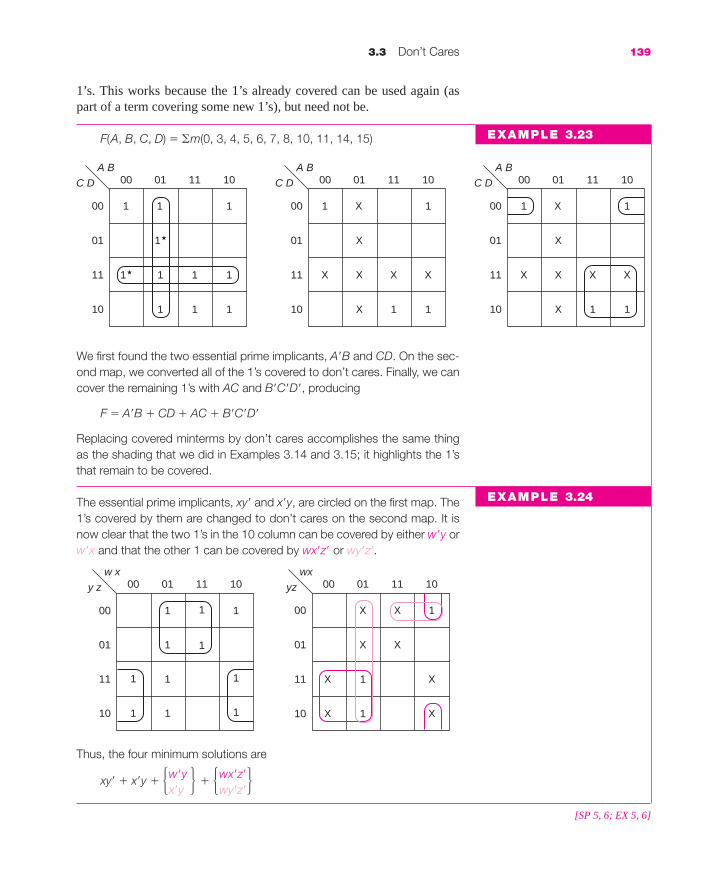
3.3 Don’t Cares 139
1’s. This works because the 1’s already covered can be used again (aspart of a term covering some new 1’s), but need not be.
F(A, B, C, D) � �m(0, 3, 4, 5, 6, 7, 8, 10, 11, 14, 15) EXAMPLE 3.23
00 01 11 10
00
01
11
10
A B
C D
111
111
11★ 1 1
1★
00 01 11 10
00
01
11
10
A B
C D
1X1
11X
XX X X
X
00 01 11 10
00
01
11
10
A B
C D
1X1
11X
XX X X
X
We first found the two essential prime implicants, A�B and CD. On the sec-ond map, we converted all of the 1’s covered to don’t cares. Finally, we cancover the remaining 1’s with AC and B�C�D�, producing
F � A�B � CD � AC � B�C�D�
Replacing covered minterms by don’t cares accomplishes the same thingas the shading that we did in Examples 3.14 and 3.15; it highlights the 1’sthat remain to be covered.
The essential prime implicants, xy� and x�y, are circled on the first map. The1’s covered by them are changed to don’t cares on the second map. It isnow clear that the two 1’s in the 10 column can be covered by either w�y orw�x and that the other 1 can be covered by wx�z� or wy�z�.
[SP 5, 6; EX 5, 6]
00 01 11 10
00
01
11
10
w x
y z
1
1
1
1 1
1 1
1
1
11
00 01 11 10
00
01
11
10
wx
yz
X 1
X 1
1X
X
X
X
X
X
EXAMPLE 3.24
Thus, the four minimum solutions are
xy� � x�y � � � � � �wx�z�
wy�z�
w�yx�y
mar91647_c03b_129_161.qxd 11/5/08 11:47 AM Page 139

3.4 PRODUCT OF SUMS
Finding a minimum product of sums expression requires no new theory.The following approach is the simplest:
1. Map the complement of the function. (If there is already a map forthe function, replace all 0’s by 1’s, all 1’s by 0’s, and leave X’sunchanged.)
2. Find the minimum sum of products expression for the complementof the function (using the techniques of the last two sections).
3. Use DeMorgan’s theorem (P11) to complement that expression,producing a product of sums expression.
Another approach, which we will not pursue here, is to define thedual of prime implicants (referred to as prime implicates) and develop anew method.
f(a, b, c, d) � �m(0, 1, 4, 5, 10, 11, 14)
Since all minterms must be either minterms of f or of f�, then f� must be thesum of all of the other minterms, that is
f�(a, b, c, d) � �m(2, 3, 6, 7, 8, 9, 12, 13, 15)
Maps of both f and f� are shown below:
We did not need to map f, unless we wanted both the sum of productsexpression and the product of sums expression. Once we mapped f, we didnot need to write out all the minterms of f�; we could have just replaced the 1’sby 0’s and 0’s by 1’s. Also, instead of mapping f�, we could look for rectanglesof 0’s on the map of f. This function is rather straightforward. The maps forthe minimum sum of product expressions for both f and f� are shown next:
00 01 11 10
00
01
11
10
a b
c d
11
1
11
f
1
1
00 01 11 10
00
01
11
10
a b
c d
11
f �
1 1 1
11
1 1
140 Chapter 3 The Karnaugh Map
EXAMPLE 3.25
mar91647_c03b_129_161.qxd 11/5/08 11:47 AM Page 140

3.4 Product of Sums 141
There is one minimum solution for f and there are two equally good solu-tions for the sum of products for f�:
f � a�c� � ab�c � acd� f� � ac� � a�c � abd
f� � ac� � a�c � bcd
We can then complement the solutions for f� to get the two minimum prod-uct of sums solutions for f:
f � (a� � c)(a � c�)(a� � b� � d�)
f � (a� � c)(a � c�)(b� � c� � d�)
The minimum sum of products solution has three terms and eight literals;the minimum product of sums solutions have three terms and seven literals.(There is no set pattern; sometimes the sum of products solution has fewerterms or literals, sometimes the product of sums does, and sometimes theyhave the same number of terms and literals.)
Find all of the minimum sum of products and all minimum product of sumssolutions for
g(w, x, y, z) � �m(1, 3, 4, 6, 11) � �d(0, 8, 10, 12, 13)
We first find the minimum sum of products expression by mapping g.However, before complicating the map by circling prime implicants, we alsomap g� (top of next page). Note that the X’s are the same on both maps.
00 01 11 10
00
01
11
10
a b
c d
11
1
11
f
1
1
00 01 11 10
00
01
11
10
a b
c d
11
f �
1 1 1
11
1 1
EXAMPLE 3.26
00 01 11 10
00
01
11
10
w x
y z
1 X XX
1
X1
11
X
00 01 11 10
00
01
11
10
w x
y z
1 X XX
1
X1★
11
X
00 01 11 10
00
01
11
10
w x
y z
X X XX
1
XX
11
Xg
mar91647_c03b_129_161.qxd 11/5/08 11:47 AM Page 141

For g, the only essential prime implicant, w�xz� is shown on the center map.The 1’s covered by it are made don’t cares on the right-hand map, and theremaining useful prime implicants are circled. We have seen similar exam-ples before, where we have three 1’s to be covered in groups of two. Thereare three equally good solutions:
g � w�xz� � � �For g�, there are three essential prime implicants, as shown on the centermap. Once all of the 1’s covered by them have been made don’t cares,there is only one 1 left; it can be covered in two ways as shown on the rightmap:
g� � x�z� � xz � wy� � � �g � (x � z)(x� � z�)(w� � y)� �
Note that in this example, the sum of products solutions each require onlythree terms (with nine literals), whereas the product of sums solutions eachrequire four terms (with eight literals).
Finally, we want to determine which, if any, of the five solutions areequal. The complication (compared to this same question in the last sec-tion) is that when we treat a don’t care as a 1 for g�, that means that we aretreating it as a 0 of g. Labeling the three sum of product solutions as g1, g2,and g3, and the two product of sums solutions as g4 and g5, we produce thefollowing table:
0 8 10 12 13
g1 1 0 0 0 0g2 0 0 0 0 0g3 0 0 1 0 0g�4 1 1 1 1 1g4 0 0 0 0 0g�5 1 1 1 1 1g5 0 0 0 0 0
(w� � x�)(w� � z)
wxwz�
w�x�y� � x�yzw�x�z � x�yzw�x�z � wx�y
142 Chapter 3 The Karnaugh Map
00 01 11 10
00
01
11
10
w x
y z
X XX
11
X1 1
11
X
00 01 11 10
00
01
11
10
w x
y z
X XX
1 1★
X1★ 1
11★
X
00 01 11 10
00
01
11
10
w x
y z
X
X X
X
X
X1X
X
X X
g�
mar91647_c03b_129_161.qxd 11/5/08 11:47 AM Page 142
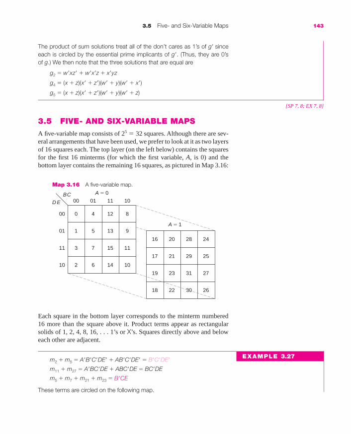
3.5 Five- and Six-Variable Maps 143
[SP 7, 8; EX 7, 8]
The product of sum solutions treat all of the don’t cares as 1’s of g� sinceeach is circled by the essential prime implicants of g�. (Thus, they are 0’sof g.) We then note that the three solutions that are equal are
g2 � w�xz� � w�x�z � x�yz
g4 � (x � z)(x� � z�)(w� � y)(w� � x�)
g5 � (x � z)(x� � z�)(w� � y)(w� � z)
3.5 FIVE- AND SIX-VARIABLE MAPS
A five-variable map consists of 25 � 32 squares. Although there are sev-eral arrangements that have been used, we prefer to look at it as two layersof 16 squares each. The top layer (on the left below) contains the squaresfor the first 16 minterms (for which the first variable, A, is 0) and thebottom layer contains the remaining 16 squares, as pictured in Map 3.16:
Each square in the bottom layer corresponds to the minterm numbered16 more than the square above it. Product terms appear as rectangularsolids of 1, 2, 4, 8, 16, . . . 1’s or X’s. Squares directly above and beloweach other are adjacent.
m2 � m5 � A�B�C�DE� � AB�C�DE� � B�C�DE�
m11 � m27 � A�BC�DE � ABC�DE � BC�DE
m5 � m7 � m21 � m23 � B�CE
These terms are circled on the following map.
00 01 11 10
00
01
11
10
B C
D E
51 13 9
40 12
A � 0
8
73 15 11
62 14 10
2117 29 25
2016 28
A � 1
24
2319 31 27
2218 30 26
Map 3.16 A five-variable map.
EXAMPLE 3.27
mar91647_c03b_129_161.qxd 11/5/08 11:47 AM Page 143

In a similar manner, six-variable maps are drawn as four layers of 16-square maps, where the first two variables determine the layer and the other variables specify the square within the layer. The layout,with minterm numbers shown, is given in Map 3.17. Note that the layersare ordered in the same way as the rows and the columns, that is 00, 01,11, 10.
In this section, we will concentrate on five-variable maps,although we will also do an example of six-variable maps at the end. Thetechniques are the same as for four-variable maps; the only thing new isthe need to visualize the rectangular solids. Rather than drawing themaps to look like three dimensions, we will draw them side by side. Thefunction, F, is mapped in Map 3.18.
F(A, B, C, D, E) � �m(4, 5, 6, 7, 9, 11, 13, 15, 16, 18, 27, 28, 31)
00 01 11 10
00
01
11
10
B C
D E
1
A � 0
1 1
1
1
A � 1
1 1
1
144 Chapter 3 The Karnaugh Map
00 01 11 10
00
01
11
10
C DE F
51 13 9
40 12
A B � 00
8
73 15 11
62 14 10
A B � 01
2117 29 25
2016 28 24
2319 31 27
2218 30 26
A B � 11
5349 61 57
5248 60 56
5551 63 59
5450 62 58
A B � 10
3733 45 41
3632 44 40
3935 47 43
3834 46 42
Map 3.17 A six-variable map.
mar91647_c03b_129_161.qxd 11/5/08 11:47 AM Page 144

As always, we first look for the essential prime implicants. A goodstarting point is to find 1’s on one layer for which there is a 0 in the cor-responding square on an adjoining layer. Prime implicants that cover that1 are contained completely on that layer (and thus, we really only have afour-variable map problem). In this example, m4 meets this criteria (sincethere is a 0 in square 20 below it). Thus, the only prime implicants cov-ering m4 must be on the first layer. Indeed, A�B�C is an essential primeimplicant. (Note that the A� comes from the fact that this group is con-tained completely on the A � 0 layer of the map and the B�C from thefact that this group is in the second column.) Actually, all four 1’s in thisterm have no counterpart on the other layer and m6 would also make thisprime implicant essential. (The other two 1’s in that term are part ofanother prime implicant, as well.) We also note that m9, m16, m18, and m28
have 0’s in the corresponding square on the other layer and make a primeimplicant essential. Although m14 has a 0 beneath it (m30), it does notmake a prime implicant on the A� layer essential. Thus, Map 3.19 showseach of these circled, highlighting the essential prime implicants that arecontained on one layer.
3.5 Five- and Six-Variable Maps 145
00 01 11 10
00
01
11
10
B C
D E
1 1
0A
1
1
1 1 1
1
1
00 01 11 10
00
01
11
10
B C
D E
1 1
1 1
1
Map 3.18 A five-variable problem.
00 01 11 10
00
01
11
10
B C
D E
1 1
0A
1★
1★
1 1 1
1★
100 01 11 10
00
01
11
10
B C
D E
1★ 1★
1 1
1★
Map 3.19 Essential prime implicants on one layer.
mar91647_c03b_129_161.qxd 11/5/08 11:47 AM Page 145

The complete solution is thus
F � A�B�C � A�BE � AB�C�E� � ABCD�E� � BDE
Groups of eight 1’s are not uncommon in five-variable problems, asillustrated in Example 3.28.
G(A, B, C, D, E ) � �m(1, 3, 8, 9, 11, 12, 14, 17, 19, 20, 22, 24, 25, 27)
The first map shows a plot of that function. On the second map, to theright, we have circled the two essential prime implicants that we found byconsidering 1’s on one layer with 0’s in the corresponding square on theother layer, A�BCE�and AB�CE�. The group of eight 1’s, C�E (also anessential prime implicant), is shown in brown on the third map (where theessential prime implicants found on the second map are shown as don’tcares). Groups of eight have three literals missing (leaving only two). At thispoint, only two 1’s are left uncovered; that requires the essential primeimplicant, BC�D�, shown on the fourth map in tan.
146 Chapter 3 The Karnaugh Map
00 01 11 10
00
01
11
10
B C
D E
1 1
0A
1★
1★
1 1 1
1★
1
00 01 11 10
00
01
11
10
B C
D E
1★ 1★
1★ 1★
1★
Map 3.20 A prime implicant covering 1’s on both layers.
EXAMPLE 3.28
So far, we have
F � A�B�C � A�BE � AB�C�E� � ABCD�E� � � � �
The two 1’s remaining uncovered do have counterparts on the other layer.However, the only prime implicant that covers them is BDE, as shown onMap 3.20 in brown. It, too, is an essential prime implicant. (Note thatprime implicants that include 1’s from both layers do not have the vari-able A in them. Such prime implicants must, of course, have the samenumber of 1’s on each layer; otherwise, they would not be rectangular.)
mar91647_c03b_129_161.qxd 11/5/08 11:47 AM Page 146

3.5 Five- and Six-Variable Maps 147
The solution is thus
G � A�BCE� � AB�CE� � C�E � BC�D�
Note that there is only one other prime implicant in this function, A�BD�E�; itcovers no 1’s not already covered.
The next problem is shown on the maps below. Once again, we start bylooking for 1’s that are on one layer, with a corresponding 0 on the otherlayer. Although there are several such 1’s on the A � 0 layer, only m10
makes a prime implicant essential. Similarly, on the A � 1 layer, m30 is cov-ered by an essential prime implicant. These terms, A�C�E� and ABCD, areshown on the second map. The 1’s covered are shown as don’t cares onthe next map.
A A
00 01 11 10
00
01
11
10
B CD E
1
0
1
1 1
1 1
1
00 01 11 10
00
01
11
10
B CD E
1
1
1
1 1
1 1
1
00 01 11 10
00
01
11
10
B CD E
1
0
1
1 1
1 1
1*
00 01 11 10
00
01
11
10
B CD E
1
1
1
1
1 1
A A
00 01 11 10
00
01
11
10
B CD E
1★
0
1
X 1
1★ 1★
X
00 01 11 10
00
01
11
10
B CD E
1★
1
1
X 1
1★ 1★
X
00 01 11 10
00
01
11
10
B CD E
1
0
1
1 1
1 1
1
00 01 11 10
00
01
11
10
B CD E
1
1
1
1 1★
1 1
1
1★
1★
A A
00 01 11 10
00
01
11
10
B CD E
1
0
1
111 1
1
11
00 01 11 10
00
01
11
10
B CD E
1
1
1
1
1 1
00 01 11 10
00
01
11
10
B CD E
1
0
1
111 1
1
1★1
00 01 11 10
00
01
11
10
B CD E
1
1
1
1
1★1
Three other essential prime implicants include 1’s from both layers of the map;they are CD�E, BCE and B�C�DE�, as shown on the left-hand map below.These were found by looking for isolated 1’s, such as m21, m15, and m18.
EXAMPLE 3.29
mar91647_c03b_129_161.qxd 11/5/08 11:47 AM Page 147
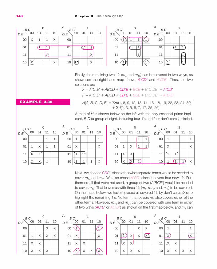
Finally, the remaining two 1’s (m4 and m12) can be covered in two ways, asshown on the right-hand map above, A�CD� and A�D�E�. Thus, the two solutions are
F � A�C�E� � ABCD � CD�E � BCE � B�C�DE� � A�CD�
F � A�C�E� � ABCD � CD�E � BCE � B�C�DE� � A�D�E�
H(A, B, C, D, E ) � �m(1, 8, 9, 12, 13, 14, 16, 18, 19, 22, 23, 24, 30)� �d(2, 3, 5, 6, 7, 17, 25, 26)
A map of H is shown below on the left with the only essential prime impli-cant, B�D (a group of eight, including four 1’s and four don’t cares), circled.
148 Chapter 3 The Karnaugh Map
Next, we choose CDE�, since otherwise separate terms would be needed tocover m14 and m30. We also chose A�BD� since it covers four new 1’s. Fur-thermore, if that were not used, a group of two (A�BCE�) would be neededto cover m12. That leaves us with three 1’s (m1, m16, and m24) to be covered.On the maps below, we have replaced all covered 1’s by don’t cares (X’s) tohighlight the remaining 1’s. No term that covers m1 also covers either of theother terms. However, m16 and m24 can be covered with one term in eitherof two ways (AC�E� or AC�D�) as shown on the first map below, and m1 can
EXAMPLE 3.30
A A
00 01 11 10
00
01
11
10
B CD E
X X X1 1
0
1
1 1 1 1
X X
X 1X
00 01 11 10
00
01
11
10
B CD E
1
1 1★
1 1 1 X
00 01 11 10
00
01
11
10
B CD E
X1
0
1 1
1 1 1 1
XX
1X X
00 01 11 10
00
01
11
10
B CD E
X
1
X
11
11 X1
A A
00 01 11 10
00
01
11
10
B CD E
X X X1 X
0
X
X X 1 1
X X
X XX
00 01 11 10
00
01
11
10
B CD E
1
X X
X X X X
00 01 11 10
00
01
11
10
B CD E
X1
0
X X
X X 1 1
XX
XX X
00 01 11 10
00
01
11
10
B CD E
X
1
X
XX
XX XX
A A
00 01 11 10
00
01
11
10
B CD E
1
0
1
11X X
1★
XX
00 01 11 10
00
01
11
10
B CD E
1★
1
1
X
1★ X
00 01 11 10
00
01
11
10
B CD E
1
0
1
111 1
1
11
00 01 11 10
00
01
11
10
B CD E
1
1
1
1
11
mar91647_c03b_129_161.qxd 11/5/08 11:47 AM Page 148

3.5 Five- and Six-Variable Maps 149
be covered by four different groups of four, as shown on the second map(A�D�E, A�B�E, B�C�E, or C�D�E ), yielding the eight solutions shown.
H � B�D � CDE� � A�BD� � � � � � �Finally, we will look at one example of a six-variable function.
G(A, B, C, D, E, F ) � �m(1, 3, 6, 8, 9, 13, 14, 17, 19, 24, 25, 29, 32,
33, 34, 35, 38, 40, 46, 49, 51, 53, 55, 56, 61, 63)
The map is drawn horizontally, with the first two variables determining the16-square layer (numbered, of course 00, 01, 11, 10).
A�D�EA�B�EB�C�EC�D�E
AC�E�
AC�D�
EXAMPLE 3.31
AB
00 01 11 10
00
01
11
10
C DE F
1 1 11 1
00
1
1 1
1★
1 1
00 01 11 10
00
01
11
10
C DE F
01
1★
00 01 11 10
00
01
11
10
C DE F
11
11
1
1★ 1 1
1 1★1
00 01 11 10
00
01
11
10
C DE F
1
10
1
111
AB
00 01 11 10
00
01
11
10
C DE F
X 1 1X 1
00
1★
X X
X
1★ 1★
00 01 11 10
00
01
11
10
C DE F
01
X
00 01 11 10
00
01
11
10
C DE F
XX
11
X
X 1 X
X XX
00 01 11 10
00
01
11
10
C DE F
X
10
X
1★11
The first map shows three of the essential prime implicants. The only one thatis confined to one layer is on the third layer, ABDF. The 1’s in the upper right-hand corner of each layer form another group of four (without the first two vari-ables), CD�E�F�. The brown squares form a group of eight, C�D�F. The nextmap shows 1’s covered by the first three prime implicants as don’t cares.
The other two essential prime implicants are A�CE�F and B�DEF�. (Remem-ber that the top and bottom layers are adjacent.) Finally, m32 and m34 (on thefourth layer) remain uncovered; they are covered by the term, AB�C�D�.(Each of them could have been covered by a group of two, but that wouldtake two terms.) Thus, the minimum expression is
G � ABDF � CD�E�F� � C�D�F � A�CE�F � B�DEF� � AB�C�D�
[SP 9, 10; EX 9, 10]
mar91647_c03b_129_161.qxd 11/5/08 11:47 AM Page 149
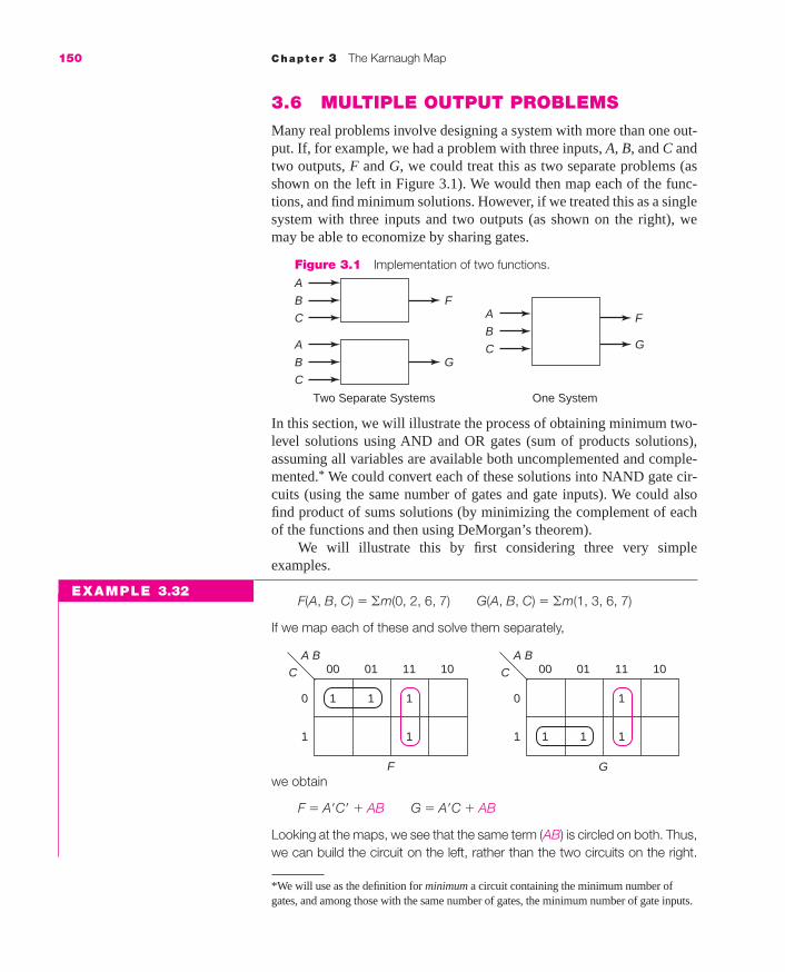
3.6 MULTIPLE OUTPUT PROBLEMS
Many real problems involve designing a system with more than one out-put. If, for example, we had a problem with three inputs, A, B, and C andtwo outputs, F and G, we could treat this as two separate problems (asshown on the left in Figure 3.1). We would then map each of the func-tions, and find minimum solutions. However, if we treated this as a singlesystem with three inputs and two outputs (as shown on the right), wemay be able to economize by sharing gates.
150 Chapter 3 The Karnaugh Map
A
B F
C
A
B G
Two Separate Systems
C
A
B
C G
F
One System
Figure 3.1 Implementation of two functions.
In this section, we will illustrate the process of obtaining minimum two-level solutions using AND and OR gates (sum of products solutions),assuming all variables are available both uncomplemented and comple-mented.* We could convert each of these solutions into NAND gate cir-cuits (using the same number of gates and gate inputs). We could alsofind product of sums solutions (by minimizing the complement of eachof the functions and then using DeMorgan’s theorem).
We will illustrate this by first considering three very simpleexamples.
F(A, B, C) � �m(0, 2, 6, 7) G(A, B, C) � �m(1, 3, 6, 7)
If we map each of these and solve them separately,
we obtain
F � A�C� � AB G � A�C � AB
Looking at the maps, we see that the same term (AB) is circled on both. Thus,we can build the circuit on the left, rather than the two circuits on the right.
00 01 11 10
0
1
A B
C
1
F
11 1
00 01 11 10
0
1
A B
C
11 1
G
1
EXAMPLE 3.32
*We will use as the definition for minimum a circuit containing the minimum number ofgates, and among those with the same number of gates, the minimum number of gate inputs.
mar91647_c03b_129_161.qxd 11/5/08 11:47 AM Page 150
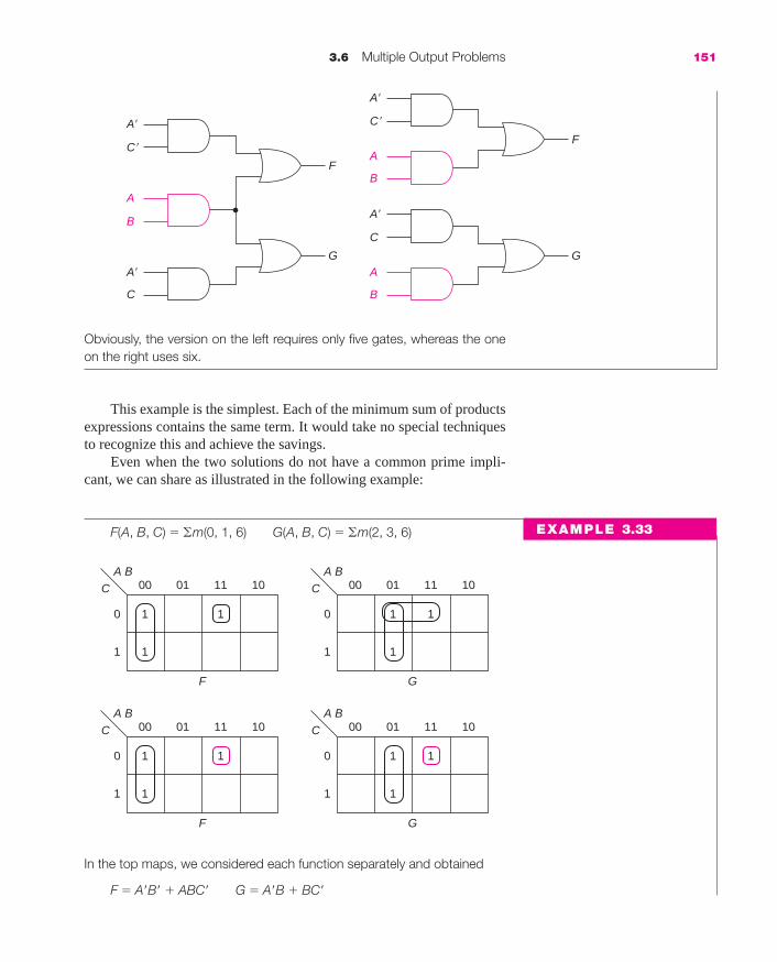
3.6 Multiple Output Problems 151
Obviously, the version on the left requires only five gates, whereas the oneon the right uses six.
This example is the simplest. Each of the minimum sum of productsexpressions contains the same term. It would take no special techniquesto recognize this and achieve the savings.
Even when the two solutions do not have a common prime impli-cant, we can share as illustrated in the following example:
F(A, B, C) � �m(0, 1, 6) G(A, B, C) � �m(2, 3, 6)
In the top maps, we considered each function separately and obtained
F � A�B� � ABC� G � A�B � BC�
00 01 11 10
0
1
A B
C
1
F
1 1
00 01 11 10
0
1
A B
C
1
G
11
00 01 11 10
0
1
A B
C
1
F
1 1
00 01 11 10
0
1
A B
C
1
G
11
A
GA�
C
B
A�
C�
F
A�
FA
B
C�
A�
GA
B
C
EXAMPLE 3.33
mar91647_c03b_129_161.qxd 11/5/08 11:47 AM Page 151

This solution requires six gates (four ANDs and two ORs) with 13 inputs.However, as can be seen from the second pair of maps, we can share theterm ABC� and obtain
F � A�B� � ABC� G � A�B � ABC�
(To emphasize the sharing, we have shown the shared term in brown, andwill do that in other examples that follow.) As can be seen from the circuitbelow, this only requires five gates with 11 inputs.
This example illustrates that a shared term in a minimum solutionneed not be a prime implicant. (In Example 3.33, ABC� is a prime impli-cant of F but not of G; in Example 3.34, we will use a term that is not aprime implicant of either function.)
F(A, B, C) � �m(2, 3, 7) G(A, B, C) � �m(4, 5, 7)
In the first pair of maps, we solved this as two problems. Using essentialprime implicants of each function, we obtained
F � A�B � BC G � AB� � AC
00 01 11 10
0
1
A B
C
F
1 1
1
00 01 11 10
0
1
A B
C
1 1
G
1
00 01 11 10
0
1
A B
C
1
F
1
1
00 01 11 10
0
1
A B
C
G
11
1
AB
GA�
B
C�
A�
B�
F
152 Chapter 3 The Karnaugh Map
EXAMPLE 3.34
mar91647_c03b_129_161.qxd 11/5/08 11:47 AM Page 152

3.6 Multiple Output Problems 153
However, as can be seen in the second set of maps, we can share the termABC, even though it is not a prime implicant of either function, and onceagain get a solution that requires only five gates:
F � A�B � ABC G � AB� � ABC
The method for solving this type of problem is to begin by lookingat the 1’s of each function that are 0’s of the other function. They must becovered by prime implicants of that function. Only the shared terms neednot be prime implicants. In this last example, we chose A�B for F sincem2 makes that an essential prime implicant of F and we chose AB� for Gsince m4 makes that an essential prime implicant of G. That left just one 1 uncovered in each function—the same 1—which we covered withABC. We will now look at some more complex examples.
F(A, B, C, D) � �m(4, 5, 6, 8, 12, 13)
G(A, B, C, D) � �m(0, 2, 5, 6, 7, 13, 14, 15)
The maps of these functions are shown below. In them, we have shown inbrown the 1’s that are included in one function and not the other.
We then circled each of those prime implicants that was made essential bya brown 1. The only brown 1 that was not circled in F is m4 because thatcan be covered by two prime implicants. Even though one of the termswould have fewer literals, we must wait. Next, we will use A�BD� for F. Sincem6 was covered by an essential prime implicant of G, we are no longer look-ing for a term to share. Thus, m6 will be covered in F by the prime implicant,A�BD�. As shown on the maps below, that leaves m4 and m12 to be coveredin both functions, allowing us to share the term BC�D, as shown on thefollowing maps circled in brown.
00 01 11 10
00
01
11
10
A B
C D
1 1★1
1
1
F
1
00 01 11 10
00
01
11
10
A B
C D
1★
11 1★
1
G
1
11
EXAMPLE 3.35
mar91647_c03b_129_161.qxd 11/5/08 11:47 AM Page 153

leaving
F � AC�D� � A�BD� � BC�D
G � A�B�D� � BC � BC�D
for a total of seven gates with 20 gate inputs. Notice that if we had mini-mized the functions individually, we would have used two separate terms forthe third term in each expression, resulting in
F � AC�D� � A�BD� � BC�
G � A�B�D� � BC � BD
for a total of eight gates with 21 gate inputs. Clearly, the shared circuit costsless.
The shared version of the circuit is shown below.*
BC�
GB
A�B�D�
C
D
A�BD�
AC�D�
F
00 01 11 10
00
01
11
10
A BC D
1 1★1
1
1
F
1
00 01 11 10
00
01
11
10
A BC D
1★
11 1★
1
G
1
11
154 Chapter 3 The Karnaugh Map
*All of these gates can be changed to NAND gates, even though the output of BC�D goes totwo places. There are still two bubbles (NOTs) in each path.
mar91647_c03b_129_161.qxd 11/5/08 11:47 AM Page 154

3.6 Multiple Output Problems 155
F(A, B, C, D) � �m(0, 2, 3, 4, 6, 7, 10, 11)
G(A, B, C, D) � �m(0, 4, 8, 9, 10, 11, 12, 13)
Once again the maps are shown with the unshared 1’s in brown and theprime implicants made essential by one of those 1’s circled.
Each of the functions can be solved individually with two more groups offour, producing
F � A�C � A�D� � B�C G � AC� � C�D� � AB�
That would require eight gates with 18 gate inputs. However, sharing thegroups of two as shown on the next set of maps reduces the number ofgates to six and the number of gate inputs to 16. If these functions wereimplemented with NAND gates, the individual solutions would require a totalof three packages, whereas the shared solution would require only two.
00 01 11 10
00
01
11
10
A B
C D
11
1
F G
1 1
00 01 11 10
00
01
11
10
A B
C D
1 1 1 1
1
1 1
11 1 1
00 01 11 10
00
01
11
10
A B
C D
11
11 1
00 01 11 10
00
01
11
10
A B
C D
1 1 1 1
1
1★ 1
11 1★ 1
EXAMPLE 3.36
mar91647_c03b_129_161.qxd 11/5/08 11:47 AM Page 155

leaving the equations and the resulting AND/OR circuit.
F � A�C � A�C�D� � AB�C G � AC� � A�C�D� � AB�C
F(W, X, Y, Z ) � �m(2, 3, 7, 9, 10, 11, 13)
G(W, X, Y, Z ) � �m(1, 5, 7, 9, 13, 14, 15)
On the maps below, the 1’s that are not shared are shown in brown and theessential prime implicants that cover these 1’s are circled.
F � X�Y � � � �
G � Y�Z � WXY � � � �
Now, there are three 1’s left in F. Since m9 and m13 have been covered in Gby an essential prime implicant, no sharing is possible for these terms in F.Thus, WY�Z, a prime implicant of F, is used in the minimum cover. Finally,there is one uncovered 1 in each function, m7; it can be covered by a sharedterm, producing the solution
00 01 11 10
00
01
11
10
W X
Y Z
11
F G
1★ 1★
00 01 11 10
00
01
11
10
W X
Y Z
1★
111★ 1
111 1 1
A�C� G
A
C�
D �
A�
C
FAB�C
156 Chapter 3 The Karnaugh Map
EXAMPLE 3.37
mar91647_c03b_129_161.qxd 11/5/08 11:47 AM Page 156

3.6 Multiple Output Problems 157
F � X�Y � WY�Z � W�XYZ
G � Y�Z � WXY � W�XYZ
This requires seven gates and 20 inputs, compared to the solution weobtain by considering these as separate problems
F � X�Y � WY�Z � W�YZ
G � Y�Z � WXY � XZ
which requires eight gates with 21 inputs.
The same techniques can be applied to problems with three or moreoutputs.
First, we show the solution obtained if we considered them as three sepa-rate problems.
00 01 11 10
00
01
11
10
W X
Y Z
11
F G
1★ 1★
00 01 11 10
00
01
11
10
W X
Y Z
1★
111★ 1
111 1 1
F � AB� � BD � B�C
G � C � A�BD
H � BC � AB�C� � (ABD or AC�D)
This solution requires 10 gates and 25 gate inputs. (Note that the term C infunction G does not require an AND gate.)
EXAMPLE 3.38
00 01 11 10
00
01
11
10
A B
C D
1
1★
11★
F
1★ 1
1 1 11
00 01 11 10
00
01
11
10
A B
C D
1★
G
1★ 1★ 1★ 1★
1★ 1 1★1★
00 01 11 10
00
01
11
10
A B
C D
H
1 1
1
1
1
1
1
mar91647_c03b_129_161.qxd 11/5/08 11:47 AM Page 157
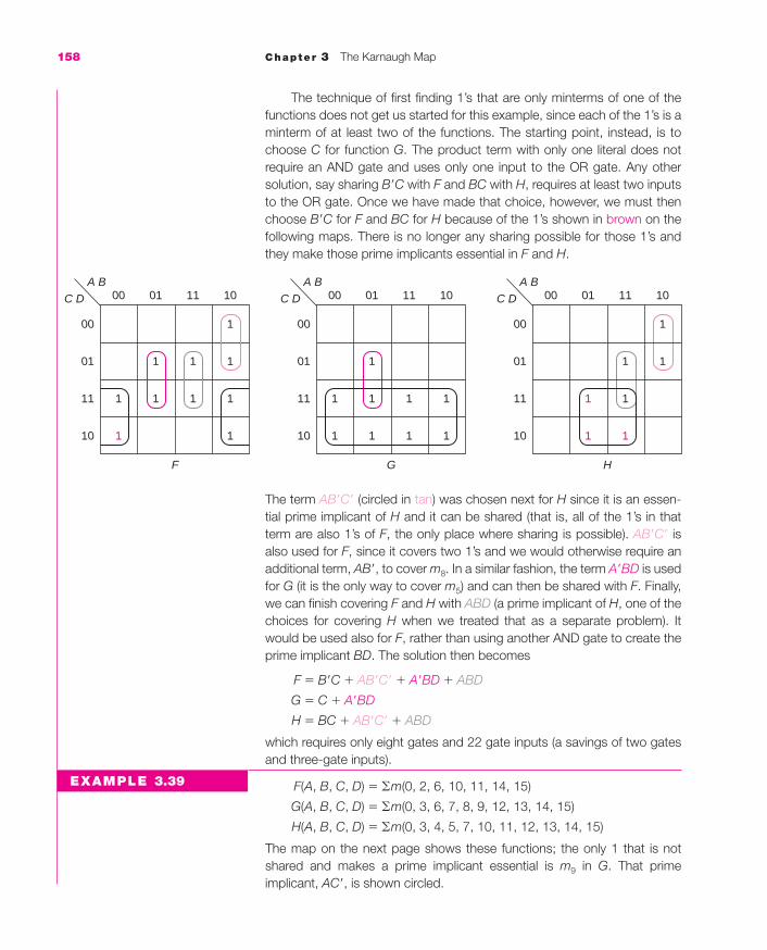
The technique of first finding 1’s that are only minterms of one of thefunctions does not get us started for this example, since each of the 1’s is aminterm of at least two of the functions. The starting point, instead, is tochoose C for function G. The product term with only one literal does notrequire an AND gate and uses only one input to the OR gate. Any othersolution, say sharing B�C with F and BC with H, requires at least two inputsto the OR gate. Once we have made that choice, however, we must thenchoose B�C for F and BC for H because of the 1’s shown in brown on thefollowing maps. There is no longer any sharing possible for those 1’s andthey make those prime implicants essential in F and H.
158 Chapter 3 The Karnaugh Map
00 01 11 10
00
01
11
10
A B
C D
1
1
11
F
1 1
1 1 11
00 01 11 10
00
01
11
10
A B
C D
1
G
1 1 1 1
1 1 11
00 01 11 10
00
01
11
10
A B
C D
H
1 1
1
1
1
1
1
EXAMPLE 3.39
The term AB�C� (circled in tan) was chosen next for H since it is an essen-tial prime implicant of H and it can be shared (that is, all of the 1’s in thatterm are also 1’s of F, the only place where sharing is possible). AB�C� isalso used for F, since it covers two 1’s and we would otherwise require anadditional term, AB�, to cover m8. In a similar fashion, the term A�BD is usedfor G (it is the only way to cover m5) and can then be shared with F. Finally,we can finish covering F and H with ABD (a prime implicant of H, one of thechoices for covering H when we treated that as a separate problem). Itwould be used also for F, rather than using another AND gate to create theprime implicant BD. The solution then becomes
F � B�C � AB�C� � A�BD � ABD
G � C � A�BD
H � BC � AB�C� � ABD
which requires only eight gates and 22 gate inputs (a savings of two gatesand three-gate inputs).
F(A, B, C, D) � �m(0, 2, 6, 10, 11, 14, 15)
G(A, B, C, D) � �m(0, 3, 6, 7, 8, 9, 12, 13, 14, 15)
H(A, B, C, D) � �m(0, 3, 4, 5, 7, 10, 11, 12, 13, 14, 15)
The map on the next page shows these functions; the only 1 that is notshared and makes a prime implicant essential is m9 in G. That primeimplicant, AC�, is shown circled.
mar91647_c03b_129_161.qxd 11/5/08 11:47 AM Page 158

3.6 Multiple Output Problems 159
Next, we note that AC is an essential prime implicant of F (because of m11
and m15) and of H (because of m10). Furthermore, neither m10 nor m11 are 1’s of G. Thus, that term is used for both F and H. Next, we chose BC� forH and BC for G; each covers four new 1’s, some of which can no longer beshared (since the 1’s that correspond to other functions have already beencovered).
At this point, we can see that A�B�C�D� can be used to cover m0 in all threefunctions; otherwise, we would need three different three-literal terms.A�CD can be used for G and H, and, finally, CD� is used for F, producing thefollowing map and algebraic functions.
00 01 11 10
00
01
11
10
A B
C D
1
F
1 111
11
00 01 11 10
00
01
11
10
A B
C D
1 1
111
G
1 1
1 1 1
00 01 11 10
00
01
11
10
A B
C D
H
11
11
111
1 1
11
00 01 11 10
00
01
11
10
A B
C D
1
F
1 111
11
00 01 11 10
00
01
11
10
A B
C D
1 1
111
G
1 1
1 1 1
00 01 11 10
00
01
11
10
A B
C D
H
11
11
111
1 1
11
00 01 11 10
00
01
11
10
A B
C D
1
F
1 111
11
00 01 11 10
00
01
11
10
A B
C D
1 1★
111
G
1 1
1 1 1
00 01 11 10
00
01
11
10
A B
C D
H
11
11
111
1 1
11
mar91647_c03b_129_161.qxd 11/5/08 11:47 AM Page 159

F � AC � A�B�C�D� � CD�
G � AC� � BC � A�B�C�D� � A�CD
H � AC � BC� � A�B�C�D� � A�CD
This solution requires 10 gates with 28 inputs, compared to 13 gates and35 inputs if these were implemented separately.
Finally, we will consider an example of a system with don’t cares:
F(A, B, C, D) � �m(2, 3, 4, 6, 9, 11, 12) � �d(0, 1, 14, 15)
G(A, B, C, D) � �m(2, 6, 10, 11, 12) � �d(0, 1, 14, 15)
A map of the functions, with the only prime implicant made essential by a 1that is not shared circled, B�D, is shown below.
Since m11 has now been covered in F, we must use the essential primeimplicant of G, AC, to cover m11 there. Also, as shown on the next maps,ABD� is used for G, since that is an essential prime implicant of G, and thewhole term can be shared. (We will share it in the best solution.)
00 01 11 10
00
01
11
10
A B
C D
X 1 1
F
1 X1
1
1★ X
X1
00 01 11 10
00
01
11
10
A B
C D
X 1
G
1 X1 1
1
X
X
00 01 11 10
00
01
11
10
A B
C D
X 1 1
F
1 X1
1
1★X
X1
00 01 11 10
00
01
11
10
A B
C D
X 1
G
1 X1 1
1
X
X
160 Chapter 3 The Karnaugh Map
EXAMPLE 3.40
mar91647_c03b_129_161.qxd 11/5/08 11:47 AM Page 160

3.6 Multiple Output Problems 161
Since we need the term ABD� for G, one approach is to use it for F also.(That only costs a gate input to the OR gate.) If we do that, we could coverthe rest of F with A�D� and the rest of G with CD�, yielding the map andequations that follow.
F � B�D � ABD� � A�D�
G � AC � ABD� � CD�
That solution uses seven gates and 17 inputs. Another solution using thesame number of gates but one more input shares A�CD�. That completesG, and then the cover of F is completed with BD�. The maps and equationsare thus:
F � B�D � A�CD� � BD�
G � AC � ABD� � A�CD�
That, too, requires seven gates, but using a three-input AND gate instead ofa two-input one, bringing the total number of inputs to 18. Thus, this solu-tion is not minimum.
00 01 11 10
00
01
11
10
A B
C D
X 1 1
F
1 X1
1
1★X
X1
00 01 11 10
00
01
11
10
A B
C D
X 1
G
1 X1 1
1
X
X
00 01 11 10
00
01
11
10
A B
C D
X 1 1
F
1 X1
1
1★X
X1
00 01 11 10
00
01
11
10
A B
C D
X 1
G
1 X1 1
1
X
X
[SP 11; EX 11, 12]
mar91647_c03b_129_161.qxd 11/5/08 11:47 AM Page 161

3.7 SOLVED PROBLEMS
1. Plot the following functions on a Karnaugh map:
a. f (a, b, c) � �m(0, 1, 3, 6)
b. g(w, x, y, z) � �m(3, 4, 7, 10, 11, 14) � �d(2, 13, 15)
c. F � BD� � ABC � AD � A�B�C
00 01 11 10
0
1
a bc
11
1 1
00 01 11 10
00
01
11
10
w x
y z
X 1
1 1X
1
X
11
00 01 11 10
00
01
11
10
A B
C D
1
1
1
1 1
1 1
1
1 1
a. b. c.
162 Chapter 3 The Karnaugh Map
c. g(a, b, c, d) � �m(0, 6, 8, 9, 10, 11, 13, 14, 15)(2 solutions)
d. f(a, b, c, d) � �m(0, 4, 5, 6, 7, 8, 9, 10, 11, 13, 14, 15)(2 solutions)
e. f(a, b, c, d) � �m(0, 1, 2, 4, 6, 7, 8, 9, 10, 11, 12, 15)
f. g(a, b, c, d) � �m(0, 2, 3, 5, 7, 8, 10, 11, 12, 13, 14, 15)(4 solutions)
00 01 11 10
0
1
X Y
Z
11 1
1 1 1
G � Y � X Z� � X� Z
00 01 11 10
0
1
X Y
Z
1★1★ 1
1★ 1 1★
a. All of the prime implicants are essential, as shown on the mapto the right.
2. For each of the following, find all minimum sum of productsexpressions. (If there is more than one solution, the number ofsolutions is given in parentheses.)
a. G(X, Y, Z) � �m(1, 2, 3, 4, 6, 7)
b. f(w, x, y, z) � �m(2, 5, 7, 8, 10, 12, 13, 15)
mar91647_c03c_162_200.qxd 11/5/08 11:48 AM Page 162

3.7 Solved Problems 163
00 01 11 10
00
01
11
10
w x
y z
11
11
1
1 1
1
00 01 11 10
00
01
11
10
w x
y z
11
11★
1★
1★ 1
1★
00 01 11 10
00
01
11
10
w x
y z
11
11
1
1 1
1
b.
The essential prime implicants are shown on the second map,leaving two 1’s to be covered. The third map shows that eachcan be covered by two different prime implicants, but thebrown group shown is the only one that covers both with oneterm. We would require both tan terms. The minimum is
f � xz � x�yz� � wy�z�
c.
00 01 11 10
00
01
11
10
a b
c d
11
11 1
1
11
1
00 01 11 10
00
01
11
10
a b
c d
11★
11★ 1
1
11★
1
00 01 11 10
00
01
11
10
a b
c d
11
11 1
1
11
1
The three essential prime implicants are shown on the centermap. The only 1 left to be covered can be covered by either oftwo groups of four, as shown circled in brown on the thirdmap, producing
g � b�c�d� � bcd� � ad � ab�
g � b�c�d� � bcd� � ad � ac
mar91647_c03c_162_200.qxd 11/5/08 11:48 AM Page 163

There are no essential prime implicants. We need one group oftwo to cover m0; all other 1’s can be covered by groups of four.Once we have chosen a�c�d� to cover m0 (center map),we would choose ab� to cover m8. (Otherwise, we must useb�c�d�, a group of two, to cover that 1. Not only is that moreliterals, but it covers nothing else new; ab� covered three addi-tional uncovered 1’s.) Once that has been done, the other twoprime implicants become obvious, giving
f � a�c�d� � ab� � bc � bd
164 Chapter 3 The Karnaugh Map
In a similar fashion (on the next map), once we choose b�c�d�(the other prime implicant that covers m0), a�b is the appropri-ate choice to cover m4:
00 01 11 10 00 01 11 10
00
01
11
10
a b
c d
11 1
11 1
1
111
11
00
01
11
10
a b
c d
11 1
11 1
1
111
11
The only way to cover the remaining 1’s in two terms is withac and ad, as shown on the second map, leaving
f � b�c�d� � a�b � ac � ad
e. There are two essential prime implicants, as indicated on thefirst map, leaving six 1’s to be covered. The essential primeimplicants are shaded on the second map.
00 01 11 10 00 01 11 10
00
01
11
10
a b
c d
11 1
11 1
1
111
11
00 01 11 10
00
01
11
10
a b
c d
11 1
11 1
1
111
11
00
01
11
10
a b
c d
11 1
11 1
1
111
11
d.
mar91647_c03c_162_200.qxd 11/5/08 11:48 AM Page 164

3.7 Solved Problems 165
1
00 01 11 10
00
01
11
10
a b
c d
11 1 1★
111
1
11★
11
00 01 11 10
00
01
11
10
a b
c d
11 1
111
1
11
11
00 01 11 10
00
01
11
10
a b
c d
11 1 1
111
1
11
11
No prime implicant covers more than two of the remaining1’s; thus, three more terms are needed. The three groups offour (two literal terms) are circled in brown on the secondmap. We can cover four new 1’s only using a�d� and ab�. Notethat m7 and m15 are uncovered; they require a group of two,bcd. The only minimum solution, requiring five terms and 11literals,
f � c�d� � b�c� � a�d� � ab� � bcd
is shown on the third map. There is another solution that usesfive terms, but it requires 12 literals, namely,
f � c�d� � b�c� � b�d� � a�bc � acd
Obviously, it is not minimum (since it has an extra literal); itonly used one of the groups of four instead of two.
f. On the second map, the two essential prime implicants havebeen highlighted (b�d� � bd), leaving four 1’s uncovered. Onthe third map, we have shown the 1’s covered by these primeimplicants shaded.
00 01 11 10
00
01
11
10
a b
c d
11 1
111
1
11
111
00 01 11 10
00
01
11
10
a b
c d
11★ 1
111
1
11★
111
00 01 11 10
00
01
11
10
a b
c d
11★ 1
111
1
11★
111
mar91647_c03c_162_200.qxd 11/5/08 11:48 AM Page 165

166 Chapter 3 The Karnaugh Map
We can cover m3 and m11 by either cd or b�c (shown withbrown lines), and we can cover m12 and m14 by either ab or ad�(shown in gray lines). Thus, there are four solutions:
f � b�d� � bd � cd � ab
f � b�d� � bd � cd � ad�
f � b�d� � bd � b�c � ab
f � b�d� � bd � b�c � ad�
The term ac is also a prime implicant. However, it is not usefulin a minimum solution since it leaves two isolated 1’s to becovered, resulting in a five-term solution.
3. For each of the following functions, find the minimum SOPexpression(s). There are two solutions for z.
00 01 11 10
00
01
11
10
a b
c d
1
1
1
1
1
1
1
1
00 01 11 10
00
01
11
10
a b
c d
1
11
1
11 1
1 1
w x
00 01 11 10
00
01
11
10
a b
c d
11
1
1
11
1
1
1
1
00 01 11 10
00
01
11
10
a b
c d
1
11
1
11
1 1
1
1
1
1
y z
All of the 1’s of w are also 1’s of the other functions. For x, weadded one 1; for y, we added a second 1; and for z, we addedtwo more. Only essential prime implicants are used for w (andthe group of four is not needed).
w = ac�d� + bc�d + acd + bcd�
mar91647_c03c_162_200.qxd 11/5/08 11:48 AM Page 166

3.7 Solved Problems 167
For x, the last three terms of w are still essential primeimplicants, as is b�c�d�. As can be seen on the next map,that leaves only m12 uncovered.
That leaves a choice between ab and ac�d�. Obviously, theformer has one less literal, leaving the minimum solution:
x = bc�d + acd + bcd� + b�c�d� + ab
For y, there are only two essential prime implicants, leavingsix 1’s to cover.
No term covers more than two of them. We must then use thegroup of four, giving
y = acd + bcd� + ab + b�c�d� + a�c�d
Finally, for z, we need 4 three-literal terms to cover the 1’s incolumns 01 and 10.
00 01 11 10
00
01
11
10
a b
c d
11
11
1
y
1
1
1★
11★
00 01 11 10
00
01
11
10
a b
c d
11
1
1
1
x
1★
1★
1★
1★
mar91647_c03c_162_200.qxd 11/5/08 12:51 PM Page 167
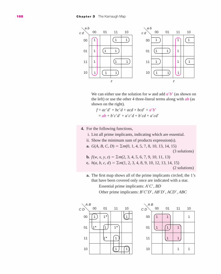
00 01 11 10
00
01
11
10
11 1★
11
1 1★1★
11★
00 01 11 10
00
01
11
10
A B
11 1
11
1 11
11
C D
A B
C D
We can either use the solution for w and add a�b� (as shown onthe left) or use the other 4 three-literal terms along with ab (asshown on the right).
f = ac�d� + bc�d + acd + bcd� + a�b�
= ab + b�c�d� + a�c�d + b�cd + a�cd�
00 01 11 10
00
01
11
10
a b
c d
11
1
1
z
1
1
1
1
1
1
1 1
00 01 11 10
00
01
11
10
a b
c d
11
1
1
z
1
1
1
1
1
1
1 1
168 Chapter 3 The Karnaugh Map
4. For the following functions,
i. List all prime implicants, indicating which are essential.
ii. Show the minimum sum of products expression(s).
a. G(A, B, C, D) � �m(0, 1, 4, 5, 7, 8, 10, 13, 14, 15)(3 solutions)
b. f (w, x, y, z) � �m(2, 3, 4, 5, 6, 7, 9, 10, 11, 13)
c. h(a, b, c, d) � �m(1, 2, 3, 4, 8, 9, 10, 12, 13, 14, 15)(2 solutions)
a. The first map shows all of the prime implicants circled; the 1’sthat have been covered only once are indicated with a star.
Essential prime implicants: A�C�, BD
Other prime implicants: B�C�D�, AB�D�, ACD�, ABC
mar91647_c03c_162_200.qxd 11/5/08 11:48 AM Page 168

3.7 Solved Problems 169
On the second map, the essential prime implicants have beenshaded, highlighting the three 1’s remaining to be covered. Weneed two terms to cover them, at least one of which mustcover two of these remaining 1’s. The three solutions are thus
F � A�C� � BD � ACD� � B�C�D�
F � A�C� � BD � AB�D� � ACD�
F � A�C� � BD � AB�D� � ABC
b.
The second map shows all of the prime implicants circled andthe 1’s that have been covered only once are indicated with astar:
Essential prime implicants: w�x, x�y
Other prime implicants: w�y, xy�z, wy�z, wx�z
With the essential prime implicants shaded on the third map, itis clear that the only minimum solution is
f � w�x � x�y � wy�z
00 01 11 10
00
01
11
10
w x
1
111
1 1 1
111
y z 00 01 11 10
00
01
11
10
w x
1★
1★11
1 1 1
111
y z 00 01 11 10
00
01
11
10
w x
1
111
1 1 1
111
y z
c. All of the prime implicants are circled on the first map, withthe essential prime implicants shown in brown.
00 01 11 10
00
01
11
10
a b
1★ 1 1
111
1 1 1
1★1
c d 00 01 11 10
00
01
11
10
a b
1 1 1
111
1 1 1
11
c d
mar91647_c03c_162_200.qxd 11/5/08 11:48 AM Page 169
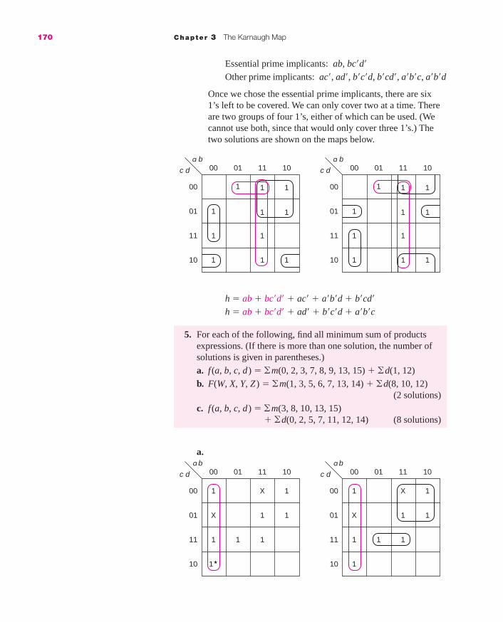
170 Chapter 3 The Karnaugh Map
a.
00 01 11 10
00
01
11
10
a b
c d
1★
1
111
X 1
X1 1
00 01 11 10
00
01
11
10
a b
c d
1
1
1
111
X 1
X 1
Essential prime implicants: ab, bc�d�
Other prime implicants: ac�, ad�, b�c�d, b�cd�, a�b�c, a�b�d
Once we chose the essential prime implicants, there are six 1’s left to be covered. We can only cover two at a time. Thereare two groups of four 1’s, either of which can be used. (Wecannot use both, since that would only cover three 1’s.) Thetwo solutions are shown on the maps below.
h � ab � bc�d� � ac� � a�b�d � b�cd�
h � ab � bc�d� � ad� � b�c�d � a�b�c
5. For each of the following, find all minimum sum of productsexpressions. (If there is more than one solution, the number ofsolutions is given in parentheses.)
a. f (a, b, c, d ) � �m(0, 2, 3, 7, 8, 9, 13, 15) � �d(1, 12)
b. F(W, X, Y, Z ) � �m(1, 3, 5, 6, 7, 13, 14) � �d(8, 10, 12)(2 solutions)
c. f (a, b, c, d ) � �m(3, 8, 10, 13, 15)� �d(0, 2, 5, 7, 11, 12, 14) (8 solutions)
00 01 11 10
00
01
11
10
a b
c d
1
1
1
1
11
1
1
1
1 1
00 01 11 10
00
01
11
10
a b
c d
1
1
1
1
11
1
1
1
1 1
mar91647_c03c_162_200.qxd 11/5/08 11:48 AM Page 170

3.7 Solved Problems 171
The first map shows the one essential prime implicant, a�b�.The remaining 1’s can be covered by two additional terms, asshown on the second map. In this example, all don’t cares aretreated as 1’s. The resulting solution is
f � a�b� � ac� � bcd
Although there are other prime implicants, such as b�c�, abd,and a�cd, three prime implicants would be needed in additionto a�b� if any of them were chosen.
b.
The second map shows all of the prime implicants circled. It is clear that only W�Z is essential, after which three 1’s remainuncovered. The prime implicant XYZ� is the only one that cancover two of these and thus appears in both minimum solu-tions. That leaves a choice of two terms to cover the remainingone—either WXY� (tan) or XY�Z (gray). Note that they treat thedon’t care at m12 differently, and, thus, although the two solu-tions shown below both satisfy the requirements of the prob-lem, they are not equal:
F � W�Z � XYZ� � WXY�
F � W�Z � XYZ� � XY�Z
00 01 11 10
00
01
11
10
W X
Y Z
111
1
1
1
X X
X
00 01 11 10
00
01
11
10
W X
Y Z
1
1
1 1 X
1
1★
1★
X X
1
00 01 11 10
00
01
11
10
W X
Y Z
1
1
1 1
1
1
1
X X
X
Also, the group of four (WZ�) is not used; that would require afour-term solution.
c. There are no essential prime implicants in this problem.The left map shows the only two prime implicants that coverm8; they also cover m10. We must choose one of these. The
mar91647_c03c_162_200.qxd 11/5/08 11:48 AM Page 171
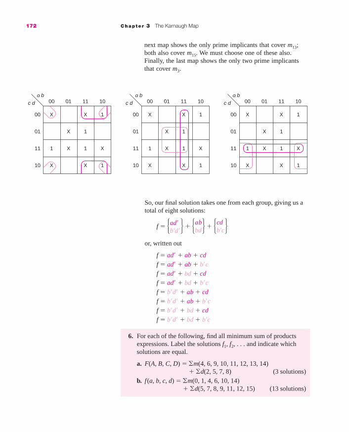
172 Chapter 3 The Karnaugh Map
00 01 11 10
00
01
11
10
a b
c d
1
1
X
X X
X
1
XX 1
00 01 11 10
00
01
11
10
a b
c d
1
1
1
X X
X X
1
X
XX 1
X 1
00 01 11 10
00
01
11
10
a b
c d
1
1
XX 1
1
XX
X
1
X X
next map shows the only prime implicants that cover m13;both also cover m15. We must choose one of these also.Finally, the last map shows the only two prime implicantsthat cover m3.
So, our final solution takes one from each group, giving us atotal of eight solutions:
f � � � � � � � � �or, written out
f � ad� � ab � cd
f � ad� � ab � b�c
f � ad� � bd � cd
f � ad� � bd � b�c
f � b�d� � ab � cd
f � b�d� � ab � b�c
f � b�d� � bd � cd
f � b�d� � bd � b�c
6. For each of the following, find all minimum sum of productsexpressions. Label the solutions f1, f2, . . . and indicate whichsolutions are equal.
a. F(A, B, C, D) � �m(4, 6, 9, 10, 11, 12, 13, 14)� �d(2, 5, 7, 8) (3 solutions)
b. f (a, b, c, d) � �m(0, 1, 4, 6, 10, 14)� �d(5, 7, 8, 9, 11, 12, 15) (13 solutions)
cdb�c
abbd
ad�b�d�
mar91647_c03c_162_200.qxd 11/5/08 11:48 AM Page 172

3.7 Solved Problems 173
a.
00 01 11 10
00
01
11
10
A B
C D
1 1X
X
X
X1 1
00 01 11 10
00
01
11
10
A B
C D
1 1
1
111
X
X
X
X11
1
1★
11
00 01 11 10
00
01
11
10
A B
C D
1 1
X 111
1
X
X11
X
On the first map, we have shown the one essential primeimplicant, AB�. Neither A�B nor CD� are essential, since the1’s covered by them can each be covered by some other primeimplicant. (That there is a don’t care that can only be coveredby one of these terms does not make that term essential.) Withfive 1’s left to be covered, we need two additional terms. Thefirst that stands out is BD�, circled on the middle map, since itcovers four of the remaining 1’s. If that is chosen, it leavesonly m13, which can be covered by BC� or AC�. However, thethird map shows still another cover, utilizing BC� and CD�.Thus, the three solutions are
F1 � AB� � BD� � BC�
F2 � AB� � BD� � AC�
F3 � AB� � BC� � CD�
Notice that none of the solutions utilize the remaining primeimplicant, A�B.
Next is the question of whether or not these three solu-tions are equal. The answer can be determined by examininghow the don’t cares are treated by each of the functions. Thefollowing table shows that:
In all functions, m7 is treated as 0 (that is, it is not included inany prime implicant used) and m8 as 1 (since it is included inthe essential prime implicant, AB�); but the first two columnsshow that no two functions treat m2 and m5 the same. Thus,none of these is equal to any other.
2 5 7 8
F1 0 1 0 1F2 0 0 0 1F3 1 1 0 1
mar91647_c03c_162_200.qxd 11/5/08 11:48 AM Page 173

174 Chapter 3 The Karnaugh Map
b. There are no essential prime implicants. The best place to startis with a 1 that can only be covered in two ways; in this prob-lem there is only one, m1. Any solution must contain either theterm a�c� (as shown on the first four maps) or the term b�c� (asshown on the remaining two maps). There is no reason to useboth, since b�c� does not cover any 1’s that are not alreadycovered by a�c�. The first map shows a�c�. Note that there arethree 1’s left, requiring two more terms. At least one of theseterms must cover two of the remaining 1’s.
00 01 11 10
00
01
11
10
a b
c d
X
X
X
X
XX
X11
1
00 01 11 10
00
01
11
10
a b
c d
111
X X
X
X
X
X
X11
1
111
00 01 11 10
00
01
11
10
a b
c d
111
X1
X
X
X
X1 1
X X
00 01 11 10
00
01
11
10
a b
c d
X
X
X
X
XX
X11
1
00 01 11 10
00
01
11
10
a b
c d
111
X X
X
X
X
X
X11
1
111
00 01 11 10
00
01
11
10
a b
c d
1
XX
X
X
X
XXX
X X
X X
The second map shows two ways of covering m6 and m14, bcand bd�. In either case, only one 1 is left to be covered. Thethird map shows the previously covered 1’s as don’t cares andthree ways of covering the last 1, m10. Thus, we have as thefirst six solutions
f1 � a�c� � bc � ab�
f2 � a�c� � bc � acf3 � a�c� � bc � ad�
f4 � a�c� � bd� � ab�
f5 � a�c� � bd� � acf6 � a�c� � bd� � ad�
Next, we consider how we may cover both m10 and m14 withone term (in addition to those already found). That providestwo more solutions shown on the left map below. (Other solu-tions that use these terms have already been listed.)
mar91647_c03c_162_200.qxd 11/5/08 11:48 AM Page 174

3.7 Solved Problems 175
f7 � a�c� � a�b � ad�
f8 � a�c� � a�b � ac
We next consider the solutions that use b�c�. The middle mapshows two of these, utilizing a�b. The last map shows the finalthree, utilizing bd�, instead; it has the same three last terms asin the first series. Thus, we have
f9 � b�c� � a�b � ad�
f10 � b�c� � a�b � ac
f11 � b�c� � bd� � ab�
f12 � b�c� � bd� � ac
f13 � b�c� � bd� � ad�
Finally, the table below shows how each of the functions treatsthe don’t cares:
Comparing the rows, the only two pairs that are equal are
f1 � f10 and f2 � f8.
7. For each of the following functions, find all of the minimumsum of products expressions and all of the minimum product ofsums expressions:
a. f (w, x, y, z) � �m(2, 3, 5, 7, 10, 13, 14, 15)(1 SOP, 1 POS solution)
b. f (a, b, c, d) � �m(3, 4, 9, 13, 14, 15) � �d(2, 5, 10, 12)(1 SOP, 2 POS solutions)
c. f (a, b, c, d) � �m(4, 6, 11, 12, 13) � �d(3, 5, 7, 9, 10, 15)(2 SOP and 8 POS solutions)
5 7 8 9 11 12 15
f1 1 1 1 1 1 0 1f2 1 1 0 0 1 0 1f3 1 1 1 0 0 1 1f4 1 0 1 1 1 1 0f5 1 0 0 0 1 1 1f6 1 0 1 0 0 1 0f7 1 1 1 0 0 1 0f8 1 1 0 0 1 0 1f9 1 1 1 1 0 1 0f10 1 1 1 1 1 0 1f11 0 0 1 1 1 1 0f12 0 0 1 1 1 1 1f13 0 0 1 1 0 1 0
mar91647_c03c_162_200.qxd 11/5/08 11:48 AM Page 175
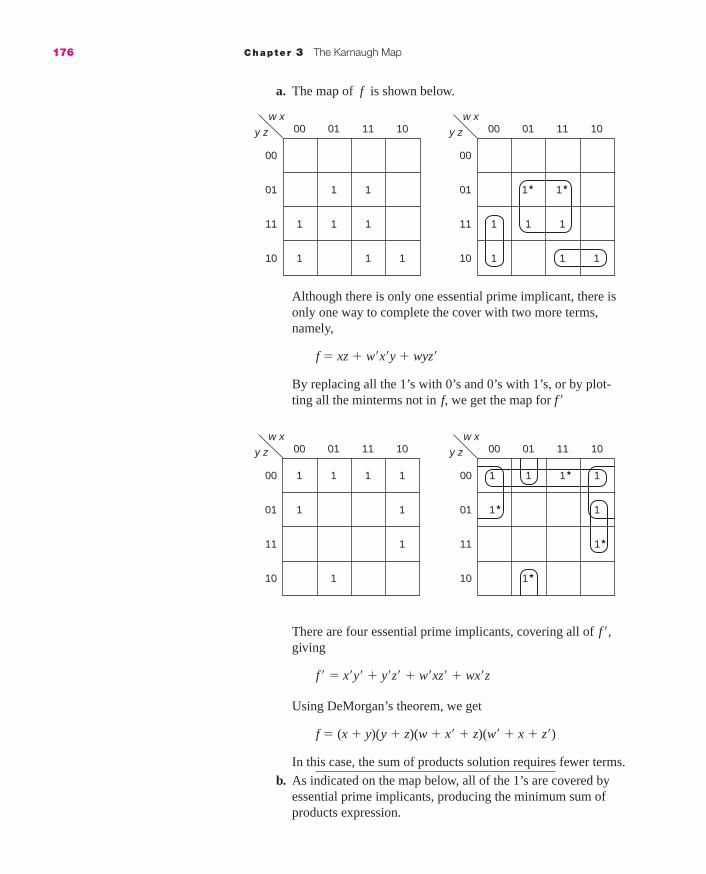
176 Chapter 3 The Karnaugh Map
a. The map of f is shown below.
Although there is only one essential prime implicant, there isonly one way to complete the cover with two more terms,namely,
f � xz � w�x�y � wyz�
By replacing all the 1’s with 0’s and 0’s with 1’s, or by plot-ting all the minterms not in f, we get the map for f �
00 01 11 10
00
01
11
10
w x
y z
1 1
11
1
1
00 01 11 10
00
01
11
10
w x
y z
11
11
1
1★
1
11
1★
00 01 11 10
00
01
11
10
w x
y z
1 1
1
1 11
1
1
00 01 11 10
00
01
11
10
w x
y z
1 1 1
1
1★
1★
1★
1★
There are four essential prime implicants, covering all of f �,giving
f � � x�y� � y�z� � w�xz� � wx�z
Using DeMorgan’s theorem, we get
f � (x � y)(y � z)(w � x� � z)(w� � x � z�)
In this case, the sum of products solution requires fewer terms.
b. As indicated on the map below, all of the 1’s are covered byessential prime implicants, producing the minimum sum ofproducts expression.
mar91647_c03c_162_200.qxd 11/5/08 11:48 AM Page 176
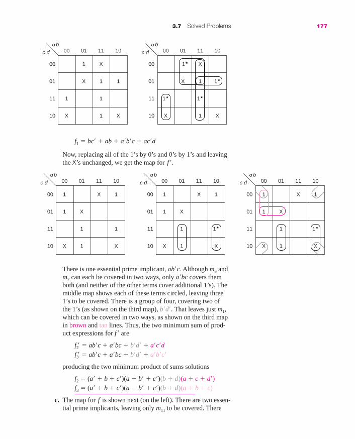
3.7 Solved Problems 177
f1 � bc� � ab � a�b�c � ac�d
Now, replacing all of the 1’s by 0’s and 0’s by 1’s and leavingthe X’s unchanged, we get the map for f �.
00 01 11 10
00
01
11
10
a b
c d
1
X
X X
X
XX
X
X
11
1
1
1
00 01 11 10
00
01
11
10
a b
c d
1
1
1★
1★1★
1★
00 01 11 10
00
01
11
10
a b
c d
11
X
XX
1
1
X 1
00 01 11 10
00
01
11
10
a b
c d
1★ 1★
X
1
X
X
X
11
1
1
00 01 11 10
00
01
11
10
a b
c d
1
1
1
1X X
X
X
1
1
There is one essential prime implicant, ab�c. Although m6 andm7 can each be covered in two ways, only a�bc covers themboth (and neither of the other terms cover additional 1’s). Themiddle map shows each of these terms circled, leaving three1’s to be covered. There is a group of four, covering two of the 1’s (as shown on the third map), b�d�. That leaves just m1,which can be covered in two ways, as shown on the third mapin brown and tan lines. Thus, the two minimum sum of prod-uct expressions for f � are
f2� � ab�c � a�bc � b�d� � a�c�d
f3� � ab�c � a�bc � b�d� � a�b�c�
producing the two minimum product of sums solutions
f2 � (a� � b � c�)(a � b� � c�)(b � d)(a � c � d�)
f3 � (a� � b � c�)(a � b� � c�)(b � d)(a � b � c)
c. The map for f is shown next (on the left). There are two essen-tial prime implicants, leaving only m11 to be covered. There
mar91647_c03c_162_200.qxd 11/5/08 11:48 AM Page 177

178 Chapter 3 The Karnaugh Map
00 01 11 10
00
01
11
10
a b
c d
1
X X
X X
X
1
1
1
00 01 11 10
00
01
11
10
a b
c d
1
X
XX
X
X
X
1★
1★
1
1
1
X
00 01 11 10
00
01
11
10
a b
c d
X
XX
X
X
X
1 1
1
00 01 11 10
00
01
11
10
a b
c d
11
XX X
X X
X
1 1 1 1
1
1
1
11
00 01 11 10
00
01
11
10
a b
c d
1
X
X
X
X
X X
Thus the two sum of products solutions are
f1 � a�b � bc� � ad
f2 � a�b � bc� � cd
We then mapped f � and found no essential prime implicants.
We chose as a starting point m8. It can be covered either by thefour corners, b�d� (as shown on the second map) or by b�c�, asshown on the third map. Whichever solution we choose, weneed a group of two to cover m14 (as shown in tan); neithercovers any other 1. After choosing one of these (and b�d�),all that remains to be covered is m1. The three brown linesshow the covers. (Notice that one of those is b�c�.) If we don’tchoose b�d�, then we must choose b�c� to cover m0 and a�b� tocover m2 (since the only other prime implicant that covers m2
is b�d�, and we have already found all of the solutions usingthat term). Thus, the eight solutions for f � are
f3� � b�d� � abc � a�b�
f4� � b�d� � abc � a�d
f5� � b�d� � abc � b�c�
are two groups of four that can be used, as indicated on theright-hand map.
mar91647_c03c_162_200.qxd 11/5/08 11:48 AM Page 178

3.7 Solved Problems 179
f6� � b�d� � acd� � a�b�
f7� � b�d� � acd� � a�d
f8� � b�d� � acd� � b�c�
f9� � b�c� � abc � a�b�
f10� � b�c� � acd� � a�b�
The product of sums solutions for f are thus
f3 � (b � d )(a� � b� � c�)(a � b)
f4 � (b � d )(a� � b� � c�)(a � d�)
f5 � (b � d )(a� � b� � c�)(b � c)
f6 � (b � d )(a� � c� � d)(a � b)
f7 � (b � d )(a� � c� � d)(a � d�)
f8 � (b � d )(a� � c�� d)(b � c)
f9 � (b � c)(a� � b� � c�)(a � b)
f10 � (b � c)(a� � c� � d)(a � b)
8. Label the solutions of each part of problem 7 as f1, f2, . . . , andindicate which solutions are equal.
a. Since this problem does not involve don’t cares, all solutionsare equal.
b.
All of the solutions are unique. The sum of products solutiontreats m2 as a 1; the product of sums treats it as a 0. The twoproduct of sums solutions treat m5 differently.
c.
For one of the sum of products expressions to be equal to one of the product of sums expressions, the pattern must be
3 5 7 9 10 15
f1 0 1 1 1 0 1f2 1 1 1 0 0 1f3� 1 0 0 0 1 1f4� 1 1 1 0 1 1f5� 0 0 0 1 1 1f6� 1 0 0 0 1 0f7� 1 1 1 0 1 0f8� 0 0 0 1 1 0f9� 1 0 0 1 0 1f10� 1 0 0 1 1 0
2 5 10 12
f1 1 1 0 1f2� 1 1 1 0f2 0 0 0 1f3� 1 0 1 0f3 0 1 0 1
mar91647_c03c_162_200.qxd 11/5/08 11:48 AM Page 179

180 Chapter 3 The Karnaugh Map
9. Find the minimum sum of products solution(s) for each of thefollowing:
a. F(A, B, C, D, E ) � �m(0, 5, 7, 9, 11, 13, 15, 18, 19, 22, 23,25, 27, 28, 29, 31)
b. F(A, B, C, D, E ) � �m(0, 2, 4, 7, 8, 10, 15, 17, 20, 21, 23,25, 26, 27, 29, 31)
c. G(V, W, X, Y, Z ) � �m(0, 1, 4, 5, 6, 7, 10, 11, 14, 15, 21, 24,25, 26, 27) (3 solutions)
d. G(V, W, X, Y, Z ) � �m(0, 1, 5, 6, 7, 8, 9, 14, 17, 20, 21, 22,23, 25, 28, 29, 30) (3 solutions)
e. H(A, B, C, D, E ) � �m(1, 3, 10, 14, 21, 26, 28, 30)� �d(5, 12, 17, 29)
a. We begin by looking at 1’s for which the correspondingposition on the other layer is 0. On the first map, all of theessential prime implicants that are totally contained on onelayer of the map, A�B�C�D�E�, A�CE, AB�D, and ABCD�, arecircled.
The 1’s covered by these essential prime implicants are shownas don’t cares on the second map. The remaining 1’s are allpart of the group of eight, BE, shown on the second map.Thus, the minimum solution is
F � A�B�C�D�E� � A�CE � AB�D � ABCD� � BE
b. On the left-hand map below, the essential prime implicants arecircled. Note that A�C�E� is on the top layer, AD�E is on thelower layer, and CDE is split between the layers.
A A
00 01 11 10
00
01
11
10
B CD E
1★
1★
0
1 1
1 1 1
00 01 11 10
00
01
11
10
B CD E
1
1
11
1
1★
1★1★
1 1
00 01 11 10
00
01
11
10
B CD E
X
X X
XX
0
1★
1★
00 01 11 10
00
01
11
10
B CD E
1
1★
X
X
1X
XX
X 1★
opposite (since we are showing the values of the don’t caresfor f� for the POS forms). Thus, f1 � f6, and f2 � f8, that is
a�b � bc� � ad � (b � d )(a� � c� � d)(a � b)
a�b � bc� � cd � (b � d )(a� � c� � d)(b � c)
mar91647_c03c_162_200.qxd 11/5/08 11:48 AM Page 180

3.7 Solved Problems 181
A A
00 01 11 10
00
01
11
10
B CD E
0
11 1★
1★
1★1★
1★ 1
00 01 11 10
00
01
11
10
B CD E
1
11
1
1
1
1 1
1
00 01 11 10
00
01
11
10
B CD E
0
1 1
1
1★1★
1★
00 01 11 10
00
01
11
10
B CD E
1
111
1
1 1 1
1
1★
1★
That leaves four 1’s to be covered, using two groups of two asshown on the right map. The minimum is thus
F � A�C�E� � AD�E � CDE � B�CD�E� � ABC�D
c. The map, with essential prime implicants circled, is shown onthe left. After choosing V�W�Y� � VWX� � W�XY�Z, there arestill six 1’s uncovered. On the right-hand map, the mintermscovered by essential prime implicants are shown as don’tcares. Each of the 1’s can be covered by two different groupsof four, which are shown on the map on the right.
V V
00 01 11 10
00
01
11
10
W XY Z
0
1
1
1★
1★
111
111
00 01 11 10
00
01
11
10
W XY Z
1
1★1★
1★
1
1 1 1 1
111
00 01 11 10
00
01
11
10
W XY Z
X
X X X X
X
X
XX
000 01 11 10
00
01
11
10
W XY Z
1
One group that covers four new 1’s must be used (or both ofthem may be used), giving the following solutions:
G � V�W�Y� � VWX� � W�XY�Z � V�XY � V�WY
G � V�W�Y� � VWX� � W�XY�Z � V�XY � WX�Y
G � V�W�Y� � VWX� � W�XY�Z � V�WY � V�W�X
d. On the first map, the two essential prime implicants, V�X�Y�and XYZ�, are circled. The term W�XZ is circled on the secondmap; if it is not used, W�XY would be needed to cover m7 andm23. But then, three more terms would be needed to cover thefunction.
mar91647_c03c_162_200.qxd 11/5/08 11:48 AM Page 181

182 Chapter 3 The Karnaugh Map
The three minimum solutions are thus
G � V�X�Y� � XYZ� � W�XZ � VY�Z � VXY�
G � V�X�Y� � XYZ� � W�XZ � VY�Z � VXZ�
G � V�X�Y� � XYZ� � W�XZ � VXY� � X�Y�Z
e. The two essential prime implicants, A�B�C�E and BDE�, arecircled on the first map. Each of the remaining 1’s can be cov-ered in two ways, by a group of two contained completely onone layer or by the group of four shown.
V V
00 01 11 10
00
01
11
10
W XY Z
X
X X
XX
0
X
X X
00 01 11 10
00
01
11
10
W XY Z
1
1
11
1
X
X
X
1
X
X X
00 01 11 10
00
01
11
10
W XY Z
X X
X
0
X
X X
00 01 11 10
00
01
11
10
W XY Z
1 X
X
X X
1
11
11
A A
00 01 11 10
00
01
11
10
B CD E
1 X
0
X
1★
1★1
00 01 11 10
00
01
11
10
B CD E
X X1
1
1
1 1★
00 01 11 10
00
01
11
10
B CD E
X
X
X
X
0
X
X
00 01 11 10
00
01
11
10
B CD E
1
1
1
X
X X
X
The following maps show the covered terms as don’t cares andthree ways of covering the remaining 1’s. On the left map, thebrown term, VY�Z, is used with either of the other terms, VXY�or VXZ�. On the right map, VXY� and X�Y�Z are used.
V V
00 01 11 10
00
01
11
10
W XY Z
1 1
1★ 1★
0
1
1
1 1★
00 01 11 10
00
01
11
10
W XY Z
1
1
11
1
1
1
1
1 1
00 01 11 10
00
01
11
10
W XY Z
1 1
1★
0
1
1★
1
1 1★
00 01 11 10
00
01
W XY Z
1 1
1
1 1
1
11
11
mar91647_c03c_162_200.qxd 11/5/08 11:48 AM Page 182

3.7 Solved Problems 183
Thus, the minimum solution is
H � A�B�C�E � BDE� � BCE� � B�D�E
10. Find the four minimum sum of products expressions for thefollowing six-variable function
G(A, B, C, D, E, F) � �m(0, 4, 6, 8, 9, 11, 12, 13, 15, 16,20, 22, 24, 25, 27, 28, 29, 31, 32, 34, 36, 38, 40, 41, 42,43, 45, 47, 48, 49, 54, 56, 57, 59, 61, 63)
On the first map, the three essential prime implicants,ABD�E�, CF, and C�DEF�, are circled in black. The first is on just the third layer. The other two include 1’s on all fourlayers (and thus do not involve the variable A and B). Also cir-cled (in brown) is a group of eight, A�E�F�, that is not essential(since each of the 1’s is part of some other prime implicant). Ifthat is not used, however, at least two terms would be neededto cover those 1’s.
AB
00 01 11 10
00
01
11
10
C DE F
1
00
1
111 1
1★1★ 1★1★
1
00 01 11 10
00
01
11
10
C DE F
1
01
1
11 11
1
00 01 11 10
00
01
11
10
C DE F
1★ 1★ 1★
1★ 1★1★
1
11
1
1
1★
00 01 11 10
00
01
11
10
C DE F
10
1
111
1
111
On the next map, the 1’s that have been covered are shown asdon’t cares. The remaining 1’s are all on the bottom (10) layer.The four corners, AB�D�F�, covers four of the five remaining1’s. Then, either AB�C�F� (on the bottom layer) or B�C�E�F�or B�C�DF� (both half on the top layer and half on the bottom)can be used to cover the remaining 1’s. These terms arecircled below.
AB
00 01 11 10
00
01
11
10
C D 00
X X
X
X X
XX
00 01 11 10
00
01
11
10
C DE FE F
01
X
X
X
X X
XX
XX
00 01 11 10
00
01
11
10
C DE F
X
X X X
X
XX
X
1101 11 10
00
01
11
10
C DE F
1 1
10
XX
X
X
X
1
11
X X
00
mar91647_c03c_162_200.qxd 11/5/08 11:48 AM Page 183

184 Chapter 3 The Karnaugh Map
H � ABD�E� � CF � C�DEF� � A�E�F� � AB�D�F�� B�C�DF�
H � ABD�E� � CF � C�DEF� � A�E�F� � AB�C�F�� AB�CD�
11. Find a minimum two-level circuit (corresponding to sum ofproducts expressions) using AND gates and one OR gate perfunction for each of the following sets of functions:
a. f (a, b, c, d ) � �m(0, 1, 2, 3, 5, 7, 8, 10, 11, 13)
g(a, b, c, d ) � �m(0, 2, 5, 8, 10, 11, 13, 15)(7 gates, 19 inputs)
b. f (a, b, c, d ) � �m(1, 2, 4, 5, 6, 9, 11, 13, 15)
g(a, b, c, d ) � �m(0, 2, 4, 8, 9, 11, 12, 13, 14, 15)(8 gates, 23 inputs)
c. F(W, X, Y, Z ) � �m(2, 3, 6, 7, 8, 9, 13)
G(W, X, Y, Z ) � �m(2, 3, 6, 7, 9, 10, 13, 14)
H(W, X, Y, Z ) � �m(0, 1, 4, 5, 9, 10, 13, 14)(8 gates, 22 inputs)
d. f (a, b, c, d ) � �m(0, 2, 3, 8, 9, 10, 11, 12, 13, 15)
g(a, b, c, d ) � �m(3, 5, 7, 12, 13, 15)
h(a, b, c, d ) � �m(0, 2, 3, 4, 6, 8, 10, 14)(10 gates, 28 inputs)
e. f (a, b, c, d ) � �m(0, 3, 5, 7) � �d(10, 11, 12, 13, 14, 15)
g(a, b, c, d ) � �m(0, 5, 6, 7, 8) � �d(10, 11, 12, 13, 14, 15)(7 gates, 19 inputs)
Also, as shown on the map below, AB�C�F� could be usedwith AB�CD�.
Thus, we have the following four solutions
H � ABD�E� � CF � C�DEF� � A�E�F� � AB�D�F�� AB�C�F�
H � ABD�E� � CF � C�DEF� � A�E�F� � AB�D�F�� B�C�E�F�
AB
00 01 11 10
00
01
11
10
C DE F
00
X X
X
X X X X X
X X
XX
X
XX
X
X
X
X
X
X
X X
X
XX
XX
XX
X
00 01 11 10
00
01
11
10
C DE F
0100 01 11 10
00
01
11
10
C DE F
1100 01 11 10
00
01
11
10
C DE F
1
1
1 1
1
10
mar91647_c03c_162_200.qxd 11/5/08 11:48 AM Page 184
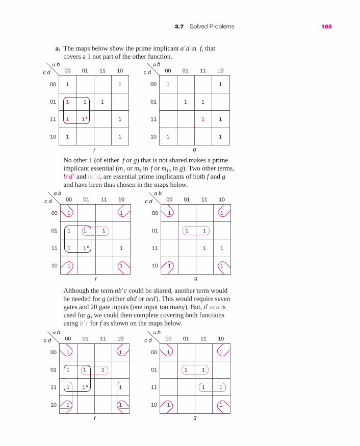
3.7 Solved Problems 185
00 01 11
f g
10
00
01
11
10
a b
c d
1
1
1
1
1 1
1
1
11
1
1
1
1
1
00 01 11 10
00
01
11
10
a b
c d
1
1
1★
No other 1 (of either f or g) that is not shared makes a primeimplicant essential (m1 or m3 in f or m15 in g). Two other terms,b�d� and bc�d, are essential prime implicants of both f and gand have been thus chosen in the maps below.
a. The maps below show the prime implicant a�d in f, thatcovers a 1 not part of the other function.
00 01 11
f g
10
00
01
11
10
a b
c d
1
1
1
1
1 1
1
1
11
1
1
1
1
1
00 01 11 10
00
01
11
10
a b
c d
1
1
1★
Although the term ab�c could be shared, another term wouldbe needed for g (either abd or acd ). This would require sevengates and 20 gate inputs (one input too many). But, if acd isused for g, we could then complete covering both functionsusing b�c for f as shown on the maps below.
00 01 11
f g
10
00
01
11
10
a b
c d
1
1
1
1
1 1
1
1
11
1
1
1
1
1
00 01 11 10
00
01
11
10
a b
c d
1
1
1★
mar91647_c03c_162_200.qxd 11/5/08 11:48 AM Page 185

186 Chapter 3 The Karnaugh Map
Next, we note that ad is an essential prime implicant of bothfunctions, producing the following maps:
00 01 11
f g
10
00
01
11
10
a b
c d
1 1
11
1 1
1
1 1
11★
11
1 1
1
00 01 11 10
00
01
11
10
a b
c d
1 1
1★
Unless we choose c�d� to cover the remaining three 1’s in thefirst row of g, we will need an extra term. Once we have donethat, we see that the last 1 (m2) of g can be covered by theminterm and shared with f. That leaves just two 1’s of f thatcan be covered with the term a�bd�. The functions and themaps are shown next:
00 01 11
f g
10
00
01
11
10
a b
c d
1 1
11
1 1
1
1 1
11★
11
1 1
1
00 01 11 10
00
01
11
10
a b
c d
1 1
1★
Thus,
f � a�d � b�d� � bc�d � b�c
g � b�d� � bc�d � acd
requiring seven gates and 19 inputs.
b. Scanning each function for 1’s that are not part of the otherfunction, we find m1, m5, and m6 in f and m0, m8, m12, and m14
in g. The only ones that make a prime implicant essential areindicated on the map below.
mar91647_c03c_162_200.qxd 11/5/08 11:48 AM Page 186

3.7 Solved Problems 187
c. When minimizing three functions, we still look for 1’s that areonly included in one of the functions and that make a primeimplicant essential. In this problem, the only ones that satisfythese conditions are m8 in F and m0 and m4 in H, as shown onthe map below.
Next, notice that W�Y is an essential prime implicant of bothF and G. Once that is chosen, the term WY�Z covers theremaining 1 of F and two 1’s in G and H. (That term would beused for both F and G in any case since it is an essential primeimplicant of both and is shareable. It is used for H since theremaining 1’s in the prime implicant Y�Z are already covered.)Finally, WYZ�, an essential prime implicant of H, finishes thecover of G and H. The maps and functions below show thefinal solution, utilizing eight gates and 22 inputs.
00 01 11
f g
10
00
01
11
10
a b
c d
1 1
11
1 1
1
1 1
11★
11
1 1
1
00 01 11 10
00
01
11
10
a b
c d
1 1
1★
00 01 11 10
00
01
11
10
W X
Y Z
1 1
1★
1
11
F G H
1
00 01 11 10
00
01
11
10
W X
Y Z
1 1
1111
11
00 01 11 10
00
01
11
10
W X
Y Z
1★ 1★
1 1
1 1
11
f � c�d � ad � a�b�cd� � a�bd�
g � ab � ad � c�d� � a�b�cd�
for a total of eight gates and 23 inputs.
mar91647_c03c_162_200.qxd 11/5/08 11:48 AM Page 187

188 Chapter 3 The Karnaugh Map
F � WX�Y� � W�Y � WY�Z
G � W�Y � WY�Z � WYZ�
H � W�Y� � WY�Z � WYZ�
d. On the maps below, the essential prime implicants that cover1’s not part of any other function are circled. In f, m9 and m11
can be covered with any of three prime implicants.
00 01 11 10
00
01
11
10
W X
Y Z
1 1
1★
1
11
F G H
1
00 01 11 10
00
01
11
10
W X
Y Z
1 1
1111
11
00 01 11 10
00
01
11
10
W X
Y Z
1★ 1★
1 1
1 1
11
00 01 11 10
00
01
11
10
a b
c d
1
1
1 1
1
1
11
f g h
1
1
00 01 11 10
00
01
11
10
a b
c d
1
1
1★
1 11
00 01 11 10
00
01
11
10
a b
c d
1★
11 1★ 1
1 1
1
Next, we note that m8 can only be covered by b�d� in h andthat b�d� is also an essential prime implicant of f. That leavesonly m3 uncovered in h; by using the minterm for that, it canbe shared with both f and g. (Otherwise, a new term would berequired in each of those functions.) The resulting maps areshown below.
mar91647_c03c_162_200.qxd 11/5/08 11:48 AM Page 188

3.7 Solved Problems 189
The only uncovered 1 in g is m12. By using abc� for both that and for f, we can cover the three remaining 1’s in f withad, yielding the maps and equations below.
00 01 11 10
00
01
11
10
a b
c d
1
1
1 1
1
1
11
f g h
1
1
00 01 11 10
00
01
11
10
a b
c d
1
1
1★
1 11
00 01 11 10
00
01
11
10
a b
c d
1★
11 1★ 1
1 1
1
00 01 11 10
00
01
11
10
a b
c d
1
1
1 1
1
1
11
f g h
1
1
00 01 11 10
00
01
11
10
a b
c d
1
1
1★
1 11
00 01 11 10
00
01
11
10
a b
c d
1★
11 1★ 1
1 1
1
f � b�d� � a�b�cd � abc� � ad
g � bd � a�b�cd � abc�
h � a�d� � cd� � b�d� � a�b�cd
e. This example includes a number of don’t cares, but that doesnot change the process significantly. There are two essentialprime implicants, cd in f and bc in g, that cover 1’s that cannotbe shared. In addition, a�b�c�d� must be used in f since it is theonly prime implicant that covers m0. (If a minterm is a primeimplicant, we have no choice but to use it.) The followingmaps show these terms circled.
mar91647_c03c_162_200.qxd 11/5/08 11:48 AM Page 189

190 Chapter 3 The Karnaugh Map
Next, we use bd to cover m5 in both functions, and completethe cover of f. The obvious choice is to use b�c�d� for theremaining 1’s of g, producing the following maps and equa-tions:
00 01 11 10
00
01
11
10
a b
c d
X X
X
X X
X X
X
X X
XX
f g
1★
1
1
1
00 01 11 10
00
01
11
10
a b
c d
11
1★
1
1
00 01 11 10
00
01
11
10
a b
c d
X X
X
X X
X X
X
X X
XX
f g
1★
1
1
1
00 01 11 10
00
01
11
10
a b
c d
11
1★
1
1
f � cd � a�b�c�d� � bd
g � bc � bd � b�c�d�
But, there is another solution, as illustrated below. By usinga�b�c�d� to cover m0 in g (we already needed that term for f ),we can cover the remaining 1 in g with a group of four, ad�,producing the solution
f � cd � a�b�c�d� � bd
g � bc � bd � a�b�c�d� � ad�
as shown on the following maps. Both solutions require sevengates and 19 inputs.
mar91647_c03c_162_200.qxd 11/5/08 11:48 AM Page 190

3.8 Exercises 191
00 01 11 10
00
01
11
10
a b
c d
X X
X
X X
X X
X
X X
XX
f g
1★
1
1
1
00 01 11 10
00
01
11
10
a b
c d
11
1★
1
1
3.8 EXERCISES1. Plot the following functions on the Karnaugh map:
a. f(a, b, c) � �m(1, 2, 3, 4, 6)★ b. g(w, x, y, z) � �m(1, 3, 5, 6, 7, 13, 14) � �d(8, 10, 12)
c. F � WX�Y�Z � W�XYZ � W�X�Y�Z� � W�XY�Z � WXYZ★ d. g � a�c � a�bd� � bc�d � ab�d � ab�cd�
e. h � x � yz� � x�z
2. For each of the following, find all minimum sum of productsexpressions. (If there is more than one solution, the number ofsolutions is given in parentheses.)
a. f (a, b, c) � �m(1, 2, 3, 6, 7)★ b. g(w, x, y) � �m(0, 1, 5, 6, 7) (2 solutions)
c. h(a, b, c) � �m(0, 1, 2, 5, 6, 7) (2 solutions)d. f (a, b, c, d ) � �m(1, 2, 3, 5, 6, 7, 8, 11, 13, 15)
★ e. G(W, X, Y, Z ) � �m(0, 2, 5, 7, 8, 10, 12, 13)f. h(a, b, c, d ) � �m(2, 4, 5, 6, 7, 8, 10, 12, 13, 15)
(2 solutions)g. f (a, b, c, d ) � �m(1, 3, 4, 5, 6, 11, 12, 13, 14, 15)
(2 solutions)h. g(w, x, y, z) � �m(2, 3, 6, 7, 8, 10, 11, 12, 13, 15)
(2 solutions)★ i. h(p, q, r, s) � �m(0, 2, 3, 4, 5, 8, 11, 12, 13, 14, 15)
(3 solutions)j. F(W, X, Y, Z ) � �m(0, 2, 3, 4, 5, 8, 10, 11, 12, 13, 14, 15)
(4 solutions)k. f (w, x, y, z) � �m(0, 1, 2, 4, 5, 6, 9, 10, 11, 13, 14, 15)
(2 solutions)l. g(a, b, c, d ) � �m(0, 1, 2, 3, 4, 5, 6, 8, 9, 10, 12, 15)
★ m. H(W, X, Y, Z ) � �m(0, 2, 3, 5, 7, 8, 10, 12, 13)(4 solutions)
EX
ER
CIS
ES
mar91647_c03c_162_200.qxd 11/5/08 11:48 AM Page 191

192 Chapter 3 The Karnaugh Map
★ n. f (a, b, c, d ) � �m(0, 1, 2, 4, 5, 6, 7, 8, 9, 10, 11, 13, 14, 15)(6 solutions)
o. g(w, x, y, z) � �m(0, 1, 2, 3, 5, 6, 7, 8, 9, 10, 13, 14, 15)(6 solutions)
★ p. f (a, b, c, d ) � �m(0, 3, 5, 6, 7, 9, 10, 11, 12, 13, 14)(32 solutions)
3. For the following functions,
i. List all prime implicants, indicating which are essential.
ii. Show the minimum sum of products expression(s).
a. f (a, b, c, d ) � �m(0, 3, 4, 5, 8, 11, 12, 13, 14, 15)★ b. g(w, x, y, z) � �m(0, 3, 4, 5, 6, 7, 8, 9, 11, 13, 14, 15)
4. Map each of the following functions and find the minimum sum ofproducts expression:
a. F � AD � AB � A�CD� � B�CD � A�BC�D�★ b. g � w�yz � xy�z � wy � wxy�z� � wz � xyz�
5. For each of the following, find all minimum sum of productsexpressions. (If there is more than one solution, the number ofsolutions is given in parentheses.) Label the solutions f1, f2, . . . .
a. f (w, x, y, z) � �m(1, 3, 6, 8, 11, 14) � �d(2, 4, 5, 13, 15)(3 solutions)
b. f (a, b, c, d ) � �m(0, 3, 6, 9, 11, 13, 14) � �d(5, 7, 10, 12)★ c. f (a, b, c, d ) � �m(0, 2, 3, 5, 7, 8, 9, 10, 11) � �d(4, 15)
(3 solutions)
d. f (w, x, y, z) � �m(0, 2, 4, 5, 10, 12, 15) � �d(8, 14)(2 solutions)
e. f (a, b, c, d ) � �m(5, 7, 9, 11, 13, 14) � �d(2, 6, 10, 12, 15)(4 solutions)
★ f. f (a, b, c, d ) � �m(0, 2, 4, 5, 6, 7, 8, 9, 10, 14) � �d(3, 13)(3 solutions)
g. f (w, x, y, z) � �m(1, 2, 5, 10, 12) � �d(0, 3, 4, 8, 13, 14, 15)(7 solutions)
6. For each of the functions of problem 5, indicate which solutionsare equal.
7. For each of the following functions, find all of the minimum sumof products expressions and all of the minimum product of sumsexpressions:
★ a. f (A, B, C, D) � �m(1, 4, 5, 6, 7, 9, 11, 13, 15)
b. f (W, X, Y, Z ) � �m(2, 4, 5, 6, 7, 10, 11, 15)
EX
ER
CIS
ES
mar91647_c03c_162_200.qxd 11/5/08 11:48 AM Page 192

3.8 Exercises 193
c. f (A, B, C, D) � �m(1, 5, 6, 7, 8, 9, 10, 12, 13, 14, 15)(1 SOP and 2 POS solutions)
★ d. f(a, b, c, d ) � �m(0, 2, 4, 6, 7, 9, 11, 12, 13, 14, 15)(2 SOP and 1 POS solutions)
e. f (w, x, y, z) � �m(0, 4, 6, 9, 10, 11, 14) � �d(1, 3, 5, 7)
f. f (a, b, c, d ) � �m(0, 1, 2, 5, 7, 9) � �d(6, 8, 11, 13, 14, 15)(4 SOP and 2 POS solutions)
g. f (w, x, y, z) � �m(4, 6, 9, 10, 11, 13) � �d(2, 12, 15)(2 SOP and 2 POS solutions)
h. f(a, b, c, d) � �m(0, 1, 4, 6, 10, 14) � �d(5, 7, 8, 9, 11, 12, 15)(13 SOP and 3 POS solutions)
i. f (w, x, y, z) � �m(1, 3, 7, 11, 13, 14) � �d(0, 2, 5, 8, 10, 12, 15)(6 SOP and 1 POS solutions)
j. f (a, b, c, d ) � �m(0, 1, 6, 15) � �d(3, 5, 7, 11, 14)(1 SOP and 2 POS solutions)
8. Label the solutions of each part of problem 7 as f1, f2, . . . andindicate which solutions are equal.
9. For each of the following five-variable functions, find all minimumsum of products expressions. (If there is more than one solution,the number of solutions is given in parentheses.)
a. F(A, B, C, D, E ) � �m(0, 1, 5, 7, 8, 9, 10, 11, 13, 15, 18, 20,21, 23, 26, 28, 29, 31)
b. G(A, B, C, D, E ) � �m(0, 1, 2, 4, 5, 6, 10, 13, 14, 18, 21, 22,24, 26, 29, 30)
★ c. H(A, B, C, D, E) � �m(5, 8, 12, 13, 15, 17, 19, 21, 23, 24, 28, 31)
d. F(V, W, X, Y, Z ) � �m(2, 4, 5, 6, 10, 11, 12, 13, 14, 15, 16,17, 18, 21, 24, 25, 29, 30, 31)
e. G(V, W, X, Y, Z ) � �m(0, 1, 4, 5, 8, 9, 10, 15, 16, 18, 19, 20,24, 26, 28, 31)
★ f. H(V, W, X, Y, Z ) � �m(0, 1, 2, 3, 5, 7, 10, 11, 14, 15, 16, 18,24, 25, 28, 29, 31) (2 solutions)
g. F(A, B, C, D, E ) � �m(0, 4, 6, 8, 12, 13, 14, 15, 16, 17, 18,21, 24, 25, 26, 28, 29, 31) (6 solutions)
h. G(A, B, C, D, E ) � �m(0, 3, 5, 7 12, 13, 14, 15, 19, 20, 21,22, 23, 25, 26, 29, 30) (3 solutions)
★ i. H(A, B, C, D, E ) � �m(0, 1, 5, 6, 7, 8, 9, 14, 17, 20, 21, 22,23, 25, 28, 29, 30) (3 solutions)
j. F(V, W, X, Y, Z ) � �m(0, 4, 5, 7, 10, 11, 14, 15, 16, 18, 20,21, 23, 24, 25, 26, 29, 31) (4 solutions)
k. G(V, W, X, Y, Z ) � �m(0, 2, 5, 6, 8, 10, 11, 13, 14, 15, 16, 17,18, 19, 20, 21, 22, 24, 26, 29, 31)
(3 solutions)
EX
ER
CIS
ES
★
mar91647_c03c_162_200.qxd 11/5/08 11:48 AM Page 193

194 Chapter 3 The Karnaugh Map
l. H(V, W, X, Y, Z ) � �m(0, 1, 2, 3, 5, 8, 9, 10, 13, 17, 18, 19,20, 21, 26, 28, 29)
(3 solutions)
m. F(A, B, C, D, E ) � �m(1, 2, 5, 8, 9, 10, 12, 13, 14, 15, 16, 18,21, 22, 23, 24, 26, 29, 30, 31)
(18 solutions)★ n. G(V, W, X, Y, Z ) � �m(0, 1, 5, 7, 8, 13, 24, 25, 29, 31)
� �d(9, 15, 16, 17, 23, 26, 27, 30)(2 solutions)
o. H(A, B, C, D, E ) � �m(0, 4, 12, 15, 27, 29, 30) � �d(1, 5, 9,10, 14, 16, 20, 28, 31)
(4 solutions)
p. F(A, B, C, D, E ) � �m(8, 9, 11, 14, 28, 30) � d(0, 3, 4, 6, 7,12, 13, 15, 20, 22, 27, 29, 31)
(8 solutions)
10. For each of the following six-variable functions, find all minimumsum of products expressions. (The number of terms and literals,and, if there is more than one solution, the number of solutions isgiven in parentheses.)
a. G(A, B, C, D, E, F ) � �m(4, 5, 6, 7, 8, 10, 13, 15, 18, 20, 21,22, 23, 26, 29, 30, 31, 33, 36, 37, 38,39, 40, 42, 49, 52, 53, 54, 55, 60, 61)
(6 terms, 21 literals)★ b. G(A, B, C, D, E, F ) � �m(2, 3, 6, 7, 8, 12, 14, 17, 19, 21, 23,
25, 27, 28, 29, 30, 32, 33, 34, 35, 40, 44,46, 49, 51, 53, 55, 57, 59, 61, 62, 63)
(8 terms, 30 literals)
c. G(A, B, C, D, E, F ) � �m(0, 1, 2, 4, 5, 6, 7, 9, 13, 15, 17, 19,21, 23, 26, 27, 29, 30, 31, 33, 37, 39,40, 42, 44, 45, 46, 47, 49, 53, 55, 57,59, 60, 61, 62, 63)
(8 terms, 28 literals, 2 solutions)
11. Find a minimum two-level circuit (corresponding to sum ofproducts expressions) using AND and one OR gate per function foreach of the following sets of functions.
★ a. f (a, b, c, d ) � �m(1, 3, 5, 8, 9, 10, 13, 14)
g(a, b, c, d ) � �m(4, 5, 6, 7, 10, 13, 14) (7 gates, 21 inputs)
b. f (a, b, c, d ) � �m(0, 1, 2, 3, 4, 5, 8, 10, 13)
g(a, b, c, d ) � �m(0, 1, 2, 3, 8, 9, 10, 11, 13)(6 gates, 16 inputs)
c. f (a, b, c, d ) � �m(5, 8, 9, 12, 13, 14)
g(a, b, c, d ) � �m(1, 3, 5, 8, 9, 10)(3 solutions, 8 gates, 25 inputs)
EX
ER
CIS
ES
mar91647_c03c_162_200.qxd 11/5/08 11:48 AM Page 194

3.8 Exercises 195
d. f (a, b, c, d ) � �m(1, 3, 4, 5, 10, 11, 12, 14, 15)
g(a, b, c, d ) � �m(0, 1, 2, 8, 10, 11, 12, 15)(9 gates, 28 inputs)
★ e. F(W, X, Y, Z ) � �m(1, 5, 7, 8, 10, 11, 12, 14, 15)
G(W, X, Y, Z ) � �m(0, 1, 4, 6, 7, 8, 12) (8 gates, 23 inputs)
f. F(W, X, Y, Z ) � �m(0, 2, 3, 7, 8, 9, 13, 15)
G(W, X, Y, Z ) � �m(0, 2, 8, 9, 10, 12, 13, 14)(2 solutions, 8 gates, 23 inputs)
g. f (a, b, c, d ) � �m(1, 3, 5, 7, 8, 9, 10)
g(a, b, c, d ) � �m(0, 2, 4, 5, 6, 8, 10, 11, 12)
h(a, b, c, d ) � �m(1, 2, 3, 5, 7, 10, 12, 13, 14, 15)(2 solutions, 12 gates, 33 inputs)
★ h. f (a, b, c, d ) � �m(0, 3, 4, 5, 7, 8, 12, 13, 15)
g(a, b, c, d ) � �m(1, 5, 7, 8, 9, 10, 11, 13, 14, 15)
h(a, b, c, d ) � �m(1, 2, 4, 5, 7, 10, 13, 14, 15)(2 solutions, 11 gates, 33 inputs)
i. f (a, b, c, d ) � �m(0, 2, 3, 4, 6, 7, 9, 11, 13)
g(a, b, c, d ) � �m(2, 3, 5, 6, 7, 8, 9, 10, 13)
h(a, b, c, d ) � �m(0, 4, 8, 9, 10, 13, 15)(2 solutions for f and g, 10 gates, 32 inputs)
★ j. f (a, c, b, d ) � �m(0, 1, 2, 3, 4, 9) � �d(10, 11, 12, 13, 14, 15)
g(a, c, b, d ) � �m(1, 2, 6, 9) � �d(10, 11, 12, 13, 14, 15)(3 solutions for f, 6 gates, 15 inputs)
k. f (a, c, b, d ) � �m(5, 6, 11) � �d(0, 1, 2, 4, 8)
g(a, c, b, d ) � �m(6, 9, 11, 12, 14) � �d(0, 1, 2, 4, 8)(2 solutions for g, 7 gates, 18 inputs)
12. In each of the following sets, the functions have been minimizedindividually. Find a minimum two-level circuit (corresponding tosum of products expressions) using AND and one OR gate perfunction for each.
a. F � B�D� � CD� � AB�C
G � BC � ACD (6 gates, 15 inputs)★ b. F � A�B�C�D � BC � ACD � AC�D�
G � A�B�C�D� � A�BC � BCD�
H � B�C�D� � BCD � AC� � AD(2 solutions for H, 10 gates, 35 inputs)
c. f � a�b� � a�d � b�c�d�
g � b�c�d� � bd � acd � abc
h � a�d� � a�b � bc�d � b�c�d� (10 gates, 31 inputs)
EX
ER
CIS
ES
mar91647_c03c_162_200.qxd 11/5/08 11:48 AM Page 195

196 Chapter 3 The Karnaugh Map
3.9 CHAPTER 3 TEST (100 MINUTES, ORTWO 50-MINUTE TESTS)
1. Map each of the following functions (be sure to label the maps):
a. f (x, y, z) � �m(1, 2, 7) � �d(4, 5)
b. g � a�c � ab�c�d � a�bd � abc�
Circle each of the terms.
2. Find the minimum sum of products expression for each of thefollowing functions (that is, circle the terms on the map and writethe algebraic expressions).
a. b.
3. Find all four minimum sum of products expressions for thefollowing function. (Two copies of the map are given for yourconvenience.)
00 01 11 10
00
01
11
10
a b
c d
11
1
1
1
11
1
1 1
1
00 01 11 10
00
01
11
10
w x
y z
1
1
1
1
1
1
1
00 01 11 10
00
01
11
10
00 01 11 10
0
1
CH
AP
TE
R T
ES
T
mar91647_c03c_162_200.qxd 11/5/08 11:48 AM Page 196

3.9 Chapter 3 Test 197
4. For the following function (three copies of the map are shown),
a. List all prime implicants, indicating which, if any, areessential.
b. Find all four minimum solutions.
00 01 11 10
00
01
11
10
a b
c d
1 11
11
11
1
11 1
1
00 01 11 10
00
01
11
10
a b
c d
1 11
11
11
1
11 1
1
00 01 11 10
00
01
11
10
w x
y z
1 X
X
1
X
X
1
1
1
X
00 01 11 10
00
01
11
10
w x
y z
1 X
X
1
X
X
1
1
1
X
00 01 11 10
00
01
11
10
w x
y z
1 X
X
1
X
X
1
1
1
X
5. For the following four-variable function, f, find both minimum sumof products expressions and both minimum product of sumsexpressions.
00 01 11 10
00
01
11
10
a b
c d
X1 1
1
X
X
X
X1
CH
AP
TE
R T
ES
T
mar91647_c03c_162_200.qxd 11/5/08 11:48 AM Page 197

198 Chapter 3 The Karnaugh Map
6. For the following function, f, find all four minimum sum ofproducts expressions and all four minimum product of sumsexpressions.
7. For the following five-variable problem, find both minimum sumof products expressions.
8. For the following five-variable problem, find both minimum sumof products expressions. (5 terms, 15 literals)
00 01
0 1
11 10
00
01
11
10
B C
D E
1
1 1
1 1
1
1
1
00 01 11 10
00
01
11
10
B C
D E
1
1
1
11 1
1
1
1
11
1
A
00 01 11 10
00
01
11
10
B C 0 1
D E
1
1
1
1
1
1
00 01 11 10
00
01
11
10
B C
D E
1
1
1
1 1
11
A
00 01 11 10
00
01
11
10
w x
y z
11
1
X
X
X
X
X
X 1
CH
AP
TE
R T
ES
T
mar91647_c03c_162_200.qxd 11/5/08 11:48 AM Page 198

3.9 Chapter 3 Test 199
9. a. For the following two functions, find the minimum sum ofproducts expression for each (treating them as two separateproblems).
b. For the same two functions, find a minimum sum of productssolution (corresponding to minimum number of gates, andamong those with the same number of gates, minimumnumber of gate inputs). (7 gates, 19 inputs)
10. Consider the three functions, the maps of which are shown below.
00 01 11 10
00
01
11
10
w x
y z
1
1
1 1
1
1
1
00 01 11 10
00
01
11
10
w x
y z
11
1 11
1
1
f g
00 01 11 10
00
01
11
10
w x
y z
1 1 1 1 1
11
1
11
11 1
1
00 01 11 10
00
01
11
10
w x
y z
1
1
11
00 01 11 10
00
01
11
10
w x
y z
1
1
1
1 1
1
1
f g h
a. Find the minimum sum of products expression (individually)for each of the three functions. Indicate which, if any, primeimplicants can be shared.
b. Find a minimum two-level NAND gate solution. Full credit fora solution using 10 gates and 32 inputs. All variables areavailable both uncomplemented and complemented. Show theequations and a block diagram.
CH
AP
TE
R T
ES
T
mar91647_c03c_162_200.qxd 11/5/08 11:48 AM Page 199

mar91647_c03c_162_200.qxd 11/5/08 11:48 AM Page 200
C H A P T E R
4
201
Function MinimizationAlgorithms
In this chapter, we will look at two approaches to finding all of theprime implicants of a function and then algorithms for finding mini-mum sum of products solutions. We will then extend the approaches
to problems with multiple outputs.The first approach to finding prime implicants is referred to as the
Quine-McCluskey method. It starts with minterms and uses, repeatedly,the adjacency property
ab � ab� � a
The second approach is iterated consensus. It starts with any set ofterms that covers the function and uses the consensus operation and theabsorption property
a � ab � a
Each of these methods has been computerized and is effective for alarger number of variables than the Karnaugh map, although the amountof computing becomes excessive for many practical problems.
4.1 QUINE-McCLUSKEY METHOD FOR ONE OUTPUT*
In this section, we will use the Quine-McCluskey method to find all ofthe prime implicants of a function. In Section 4.3, we will use that set ofprime implicants to find the minimum sum of products expression(s) forthat function. We start with a list of minterms, in numerical form (that is,1 for an uncomplemented variable and 0 for a complemented one). If westart with minterm numbers, this is just the binary equivalent of theminterm number. We order this list by the number of 1’s in each term. Wewill use the function of Example 3.6:
f(w, x, y, z) � �m(0, 4, 5, 7, 8, 11, 12, 15)
*The Quine-McCluskey algorithm was developed by W. V. Quine and Edward J.McCluskey in the 1950s.
mar91647_c04_201_248.qxd 11/5/08 10:40 AM Page 201

202 Chapter 4 Function Minimization Algorithms
Our initial list, grouped by the number of 1’s, is
A 0 0 0 0
--------
B 0 1 0 0
C 1 0 0 0
--------
D 0 1 0 1
E 1 1 0 0
--------
F 0 1 1 1
G 1 0 1 1
--------
H 1 1 1 1
where we have labeled the terms for easy reference.We now apply the adjacency property to each pair of terms. Since
that property requires all the variables to be the same except for one, weneed only consider terms in consecutive groups. We produce a secondcolumn of terms with one variable missing:
A � B � J � 0 – 0 0 (where the dash represents a missingvariable)
A � C � K � – 0 0 0
B � D � L � 0 1 0 –
B � E � M � – 1 0 0
C � D � none
C � E � N � 1 – 0 0
D � F � O � 0 1 – 1
D � G � none
E � F � none
E � G � none
F � H � P � – 1 1 1
G � H � Q � 1 – 1 1
Of course, some pairs of terms, even in adjacent groups, cannot be com-bined because they differ in more than one place, such as terms C and D.Whenever a term is used to produce another term, it is checked off; it isnot a prime implicant. These (three literal) terms are placed in a secondcolumn as shown in Table 4.1. All of the minterms have been used toform at least one term in the second column; thus, no minterms are primeimplicants.
We now repeat the process with the second column. Again, we needonly consider terms in consecutive sections of that column (number of
mar91647_c04_201_248.qxd 11/5/08 10:40 AM Page 202

4.1 Quine-McCluskey Method for One Output 203
Table 4.1 Quine-McCluskey prime implicant computation.
A 0 0 0 0 √ J 0 – 0 0 √ R – – 0 0------------- K – 0 0 0 √B 0 1 0 0 √ -------------C 1 0 0 0 √ L 0 1 0 –------------- M – 1 0 0 √D 0 1 0 1 √ N 1 – 0 0 √E 1 1 0 0 √ -------------------------- O 0 1 – 1F 0 1 1 1 √ -------------G 1 0 1 1 √ P – 1 1 1------------- Q 1 – 1 1 H 1 1 1 1 √
1’s differing by only one). Also, we need only consider terms withdashes in the same position, since they are the only ones with the samethree variables. Thus, we find
J � N � R � – – 0 0
K � M � R (same term)
Each term in this column is always formed by two different pairs ofterms. In this example, y�z� is formed by the computation w�y�z� + wy�z�as well as by x�y�z� + xy�z�, as shown on the map below. (Note that onlythese terms of the function are shown.)
There are no adjacencies between the second and third group or betweenthe third and fourth group.
Since there is only one term in the third column, we are done. Ifthere were more terms, we would repeat the process, forming a columnwith three literals missing (corresponding to a group of eight minterms).The prime implicants are
L 0 1 0 – w�xy�
O 0 1 – 1 w�xz
P – 1 1 1 xyz
Q 1 – 1 1 wyz
R – – 0 0 y�z�
00 01 11 10
00
01
11
10
11 1 1
w x
y z
mar91647_c04_201_248.qxd 11/5/08 10:40 AM Page 203

204 Chapter 4 Function Minimization Algorithms
[SP 1; EX 1]
EXAMPLE 4.1
If there are don’t cares in the problem, all of them must be included in thefirst column of the table, since don’t cares are part of prime implicants.
g(w, x, y, z) � �m(1, 3, 4, 6, 11) � �d(0, 8, 10, 12, 13)
The process proceeds as before
0 0 0 0 √ 0 0 0 – – – 0 0-------- 0 – 0 0 √0 0 0 1 √ – 0 0 0 √0 1 0 0 √ --------1 0 0 0 √ 0 0 – 1-------- 0 1 – 00 0 1 1 √ – 1 0 0 √0 1 1 0 √ 1 0 – 01 0 1 0 √ 1 – 0 0 √1 1 0 0 √ ---------------- – 0 1 11 0 1 1 √ 1 0 1 –1 1 0 1 √ 1 1 0 –
Thus, the prime implicants are
w�x�y� x�yzw�x�z wx�yw�xz� wxy�
wx�z� y�z�
Although wxy� and wx�z� are prime implicants, they consist of all don’t caresand would never be used in a minimum solution.
This process works for larger number of variables, but the number ofminterms and other implicants can increase rapidly. We will see oneexample with five variables in the solved problems. This process hasbeen computerized.
4.2 ITERATED CONSENSUSFOR ONE OUTPUT
In this section, we will use the iterated consensus algorithm to list all ofthe prime implicants of a function. In the next section, we will use thatlist to find the minimum sum of products expression(s).
To simplify the discussion, we will first define the relationshipincluded in.
Product term t1 is included in product term t2 (written t1 � t2) if t2 is 1whenever t1 is 1 (and elsewhere, too, if the two terms are not equal).*
*The relationship included in is also applied to more complex functions than productterms, but that will not be important here.
mar91647_c04_201_248.qxd 11/5/08 10:40 AM Page 204

4.2 Iterated Consensus for One Output 205
All this really means for product terms is that either t1 � t2, or t1 � xt2,where x is a literal or a product of literals. From the perspective of themap, it means that t1 is a subgroup of t2. If an implicant, t1, is included inanother implicant, t2, then t1 is not a prime implicant since
t1 � t2 � xt2 � t2 � t2 [P12a]
The iterated consensus algorithm for single functions is as follows:
1. Find a list of product terms (implicants) that cover the function.Make sure that no term is equal to or included in any other term on the list. (The terms on the list could be prime implicants orminterms or any other set of implicants. However, the rest of thealgorithm proceeds more quickly if we start with prime implicants.)
2. For each pair of terms, ti and tj (including terms added to the list instep 3), compute ti ¢ tj.
3. If the consensus is defined, and the consensus term is not equal toor included in a term already on the list, add it to the list.
4. Delete all terms that are included in the new term added to the list.
5. The process ends when all possible consensus operations havebeen performed. The terms remaining on the list are ALL of theprime implicants.
Consider the following function (Example 3.6 from Chapter 3 andthe function we used to describe the Quine-McCluskey method inSection 4.1).
f(w, x, y, z) � �m(0, 4, 5, 7, 8, 11, 12, 15)
We chose as a starting point a set of product terms that cover the func-tion; they include some prime implicants and a minterm, as well as otherimplicants.
A w�x�y�z�B w�xy�C wy�z�D xyzE wyz
We labeled the terms for reference and go in the order, B ¢ A, C ¢ B,C ¢ A, D ¢ C, . . . , omitting any computation when the term has beenremoved from the list. When a term is removed, we cross it out. The firstconsensus, B ¢ A, produces w�y�z�; A is included in that term and canthus be removed. After the first step, the list becomes
A w�x�y�z�B w�xy�C wy�z�D wyzE wyzF w�y�z�
mar91647_c04_201_248.qxd 11/5/08 10:40 AM Page 205

206 Chapter 4 Function Minimization Algorithms
Table 4.3 Numeric computation of prime implicants.
A 0 0 0 0
B 0 1 0 –
C 1 – 0 0
D – 1 1 1
E 1 – 1 1
F 0 – 0 0 B ¢ A � A
G – 1 0 0 C ¢ B
H 0 1 – 1 D ¢ B (D ¢ C undefined)
(E ¢ D, E ¢ C, E ¢ B, F ¢ E, F ¢ D undefined)J – – 0 0 F ¢ C � G, F, C
(H ¢ E � D; H ¢ D, H ¢ B undefined; J ¢ H � B;J ¢ E, J ¢ D, J ¢ B undefined)
Table 4.2 Computing the primeimplicants.
A w�x�y�z�B w�xy�C wy�z�D xyzE wyzF w�y�z� B ¢ A � A (remove A)G xy�z� C ¢ B
D ¢ C undefinedH w�xz D ¢ B
E ¢ D undefinedE ¢ C undefinedE ¢ B undefinedF ¢ E undefinedF ¢ D undefined
J y�z� F ¢ C � G, F, C(remove G, F, C )
H ¢ E � D (do not add)H ¢ D undefinedH ¢ B undefinedJ ¢ H � B (do not add)J ¢ E undefinedJ ¢ D undefinedJ ¢ B undefined
We next find C ¢ B, which creates term G, xy�z�; it is not includedin any other term and no other term is included in it. There is no needto compute C ¢ A, since term A has already been removed fromthe list.
The complete computation is shown in Table 4.2, where each possi-ble consensus is listed on a separate line.
The terms that remain, B, D, E, H, and J, that is, w�xy, xyz, wyz,w�xz, and y�z�, are all the prime implicants. The minimum sum of prod-ucts expression(s) will use some of these, typically not all of them.
The process can be simplified by using a numeric representation ofthe terms. As in the truth table, a 0 represents a complemented variable,and a 1 represents an uncomplemented variable. If a variable is missingfrom a term, as we did in Quine-McCluskey, a dash (–) is used in itsplace so that each term has four entries. A consensus exists if there is a1 for exactly one variable in one term and a 0 for that variable in theother. The consensus term has a 1 for a variable if one term has a 1 andthe other either a 1 or a –; it has a 0 if one term has a 0 and the other a0 or a –, and a – if one term has a 0 and the other a 1 or if both termshave a –. For the function of Table 4.2, the process becomes that ofTable 4.3 (where we have not left lines for consensus operations that areundefined).
The five terms remaining in Table 4.3 are the same as those inTable 4.2.
If there are don’t cares in the function, all of them must be includedin at least one of the terms to start the process. The resulting list of primeimplicants will then include all possible prime implicants (includingpossibly some that are made up of only don’t cares). The prime implicanttable will then allow us to choose the minimum cover.
mar91647_c04_201_248.qxd 11/5/08 10:40 AM Page 206
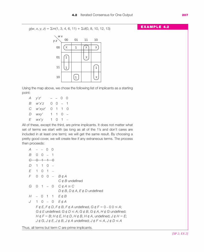
g(w, x, y, z) � �m(1, 3, 4, 6, 11) � �d(0, 8, 10, 12, 13)
Using the map above, we chose the following list of implicants as a startingpoint:
A y�z� – – 0 0
B w�x�z 0 0 – 1
C w�xyz� 0 1 1 0
D wxy� 1 1 0 –
E wx�y 1 0 1 –
All of these, except the third, are prime implicants. It does not matter whatset of terms we start with (as long as all of the 1’s and don’t cares areincluded in at least one term); we will get the same result. By choosing apretty good cover, we will create few if any extraneous terms. The processthen proceeds:
A – – 0 0
B 0 0 – 1
C 0 1 1 0
D 1 1 0 –
E 1 0 1 –
F 0 0 0 – B ¢ AC ¢ B undefined
G 0 1 – 0 C ¢ A � CD ¢ B, D ¢ A, E ¢ D undefined
H – 0 1 1 E ¢ B
J 1 0 – 0 E ¢ A
F ¢ E, F ¢ D, F ¢ B, F ¢ A undefined, G ¢ F � 0 – 0 0 � A;G ¢ E undefined; G ¢ D � A; G ¢ B, G ¢ A, H ¢ G undefined; H ¢ F � B; H ¢ E, H ¢ D, H ¢ B, H ¢ A, undefined; J ¢ H � E;J ¢ G, J ¢ E, J ¢ B, J ¢ A undefined; J ¢ F � A, J ¢ D � A
Thus, all terms but term C are prime implicants.
00 01 11 10
00
01
11
10
XX
1 X
1 1
1 X
w x
y z
X1
4.2 Iterated Consensus for One Output 207
EXAMPLE 4.2
[SP 2; EX 2]
mar91647_c04_201_248.qxd 11/5/08 10:40 AM Page 207

208 Chapter 4 Function Minimization Algorithms
Table 4.4 A prime implicant (PI) table.
PI Numeric $ Label 0 4 5 7 8 11 12 15
w�xy� 0 1 0 – 4 A X X
xyz – 1 1 1 4 B X X
wyz 1 – 1 1 4 C X X
w�xz 0 1 – 1 4 D X X
y�z� – – 0 0 3 E X X X X
4.3 PRIME IMPLICANT TABLESFOR ONE OUTPUT
Once we have a complete list of prime implicants, using either Quine-McCluskey or iterated consensus, a table is constructed with one row foreach prime implicant and one column for each minterm included in thefunction (not don’t cares). An X is entered in the column of a mintermthat is covered by that prime implicant. Thus, for the prime implicants ofthe first function, f, in both Sections 4.1 and 4.2, the prime implicanttable is shown in Table 4.4.
The first column is the list of prime implicants in algebraic form; thesecond is in numeric form.* The latter makes it easy to find a list of minterms that are covered by this term, since each – can representeither a 0 or a 1. For example, term 010– covers minterms 0100 (4) and 0101 (5). The third column is the number of gate inputs when that termis used in a two-level circuit, that is, just one for each literal plus one forthe input to the output gate (OR). The fourth column is just the label (tosave writing the whole term later). We will label terms in alphabeticorder. (They may differ from the labeling of these terms in Sections 4.1and 4.2.)
Our job is to find a minimum set of rows such that using only theserows, every column has at least one X, that is, all of the minterms areincluded in the expression. If there is more than one set, the total numberof gate inputs ($ column) is minimized. The first step in the process isto find essential prime implicants. They correspond to rows where the Xis the only one in at least one column. Those squares are shaded; theminterms covered by each of the essential prime implicants are checkedoff; and an asterisk is placed next to the prime implicant as shown inTable 4.5.
*The order of the list is not important. The two methods used to find prime implicantsproduced the same list but in different order.
mar91647_c04_201_248.qxd 11/5/08 10:40 AM Page 208

4.3 Prime Implicant Tables for One Output 209
Table 4.5 Finding essential prime implicants.
√ √ √ √ √ √
PI Numeric $ Label 0 4 5 7 8 11 12 15
w�xy� 0 1 0 – 4 A X X
xyz – 1 1 1 4 B X X
wyz★ 1 – 1 1 4 C X X
w�xz 0 1 – 1 4 D X X
y�z�★ – – 0 0 3 E X X X X
Table 4.6 The reducedtable.
$ Label 5 7
4 A X
4 B X
4 D X X
EXAMPLE 4.3
Note that all of the minterms covered by the essential prime implicantsare checked, not just those columns with shaded X’s. The table is nowreduced to that of Table 4.6 by eliminating the essential prime implicantrows and the covered minterms.
In this simple example, the answer is apparent. Prime implicant Hcovers the remaining 1’s; any other solution would require at least twomore terms, for a total of four. Thus, the solution is
C � E � D � wyz � y�z� � w�xz
Before looking at some more complex examples that will require usto develop additional techniques, we will complete Examples 4.1 and 4.2(with don’t cares), for which we have already developed a list of primeimplicants. The only thing that is different from the first example is thatwe only have columns for minterms included in the function—not fordon’t cares. That is really what happened in the reduced table above; thecolumns that were eliminated correspond to minterms that became don’tcares after having chosen the essential prime implicants (as in MapMethod 3).
√ √PI $ Label 1 3 4 6 11
y�z� – – 0 0 3 A X
w�x�z 0 0 – 1 4 B X X
wxy� 1 1 0 – 4 C
wx�y 1 0 1 – 4 D X
w�x�y� 0 0 0 – 4 E X
w�xz�★ 0 1 – 0 4 F X X
x�yz – 0 1 1 4 G X X
wx�z� 1 0 – 0 4 H
mar91647_c04_201_248.qxd 11/5/08 10:40 AM Page 209

210 Chapter 4 Function Minimization Algorithms
EXAMPLE 4.4
The first thing to note about this table is that rows C and H have no X’s inthem; they correspond to prime implicants that cover only don’t cares. F isessential, as indicated by the shading. We can now eliminate rows C, H,and F and columns 4 and 6, producing the reduced table:
Note that row A has no X’s; the minterm that it covered was already coveredby the essential prime implicant. There are several ways to proceed fromhere. By looking at the table, we can see that we need at least one primeimplicant that covers two minterms (either B or G). In either case, oneminterm is left. There are three solutions:
F � B � D � w�xz� � w�x�z � wx�y
F � B � G � w�xz� � w�x�z � x�yz
F � G � E � w�xz� � x�yz � w�x�y�
All of these are equal cost, since each of the prime implicants used have thesame number of literals. (We will see in other examples that some of thecovers that use the same number of terms may have a different number ofliterals.)
If we are looking for only one of the minimum solutions, instead ofall of them, we can often reduce a prime implicant table by removingdominated or equal rows. A row dominates another if the term it repre-sents costs no more than the other and has X’s in every column that thedominated row does (and possibly more).
In Example 4.3, row E is dominated by B, and row D is dominated by G.Removing the dominated rows, the table reduces to
and the only solution produced is
F � B � G � w�xz� � w�x�z � x�yz
Finally, a third approach, called Petrick’s method, utilizes the tablewe have obtained after removing the essential prime implicants, but
$ Label 1 3 11
4 B X X
4 G X X
$ Label 1 3 11
3 A
4 B X X
4 D X
4 E X
4 G X X
mar91647_c04_201_248.qxd 11/5/08 10:40 AM Page 210

4.3 Prime Implicant Tables for One Output 211
EXAMPLE 4.5
before removing dominated and equal rows. Create a product of sumsexpression by producing one term for each column. For the last example,the expression is
(B � E)(B � G)(D � G)
Minterm 1 must be covered by B or E, minterm 3 by B or G, and minterm11 by E or G. Expanding that expression to sum of products form, we get
(B � EG)(D � G) � BD � BG � DEG � EG� BD � BG � EG
Each product term corresponds to a set of prime implicants that could beused to cover the function. These are, of course, the solutions that wefound.
We are now ready to look at some more complex examples.
f(a, b, c, d) � �m(1, 3, 4, 6, 7, 9, 11, 12, 13, 15)
From the map, Quine-McCluskey, or iterated consensus,* we could find allof the prime implicants and construct the following table:
*An effective approach is to map the function and find as many prime implicants aspossible. Then, use iterated consensus to check that none have been left out.
There is one essential prime implicant, b�d, as shown in the table above.The table is then reduced, by eliminating that row and the terms that havebeen covered.
√ √ √ √$ 1 3 4 6 7 9 11 12 13 15
b�d★ – 0 – 1 3 A X X X X
cd – – 1 1 3 B X X X X
ad 1 – – 1 3 C X X X X
abc� 1 1 0 – 4 D X X
bc�d� – 1 0 0 4 E X X
a�bd� 0 1 – 0 4 F X X
a�bc 0 1 1 – 4 G X X
$ 4 6 7 12 13 15
3 B X X
3 C X X
4 D X X
4 E X X
4 F X X
4 G X X
mar91647_c04_201_248.qxd 11/5/08 10:40 AM Page 211

212 Chapter 4 Function Minimization Algorithms
The reduced table has two X’s in each column and two X’s in each row.Since there are six minterms to be covered, we need at least three primeimplicants. Also, since B and C cost less than the other terms, we shouldtry to use them. A careful study of the table will show that there are two cov-ers that use three terms, each of which uses one of the less costly terms,namely,
A � B � D � F � b�d � cd � abc� � a�bd�
A � C � E � G � b�d � ad � bc�d� � a�bc
(We cannot complete the cover with three terms in addition to A by usingboth of the less costly rows, since they only cover three 1’s between them.)The more systematic approach is to choose one of the minterms that canbe covered in the fewest number of ways, for example, 4. We then recog-nize that we must choose either E or F in order to cover minterm 4. We willnext derive a minimum solution using each of those and compare them.After we choose E, the table reduces to
Note that row D is dominated by C and costs more than C. It can beremoved. (This row is shaded in the table above.) If that is eliminated, C isneeded to cover minterm 13. (It also covers minterm 15.) Now, onlyminterms 6 and 7 need to be covered; the only way to do that with one termis with G. That produces the solution
A � C � E � G
Row F is also dominated (by G); but those two terms cost the same. Ingeneral (although not in this example), we risk losing other equally goodsolutions if we delete dominated rows that are not more expensive.
If, instead, we chose prime implicant F to cover minterm 4, we wouldhave
$ 6 7 13 15
3 B X X
3 C X X
4 D X
4 F X
4 G X X
$ 7 12 13 15
3 B X X
3 C X X
4 D X X
4 E X
4 G X
mar91647_c04_201_248.qxd 11/5/08 10:40 AM Page 212

4.3 Prime Implicant Tables for One Output 213
EXAMPLE 4.6
Row G is dominated by row B and costs more. Thus, prime implicant B isneeded to cover the function. With only minterms 12 and 13 left, we mustchoose term D, giving the other solution
A � F � B � D
Finally, we could go back to the second table (with six minterms) and con-sider the prime implicants needed to cover each minterm. Petrick’s methodproduces the following expression
(E � F )(F � G)(B � G)(D � E )(C � D)(B � C)
� (F � EG)(B � CG)(D � CE )
� (BF � BEG � CFG � CEG)(D � CE )
� BDF � BDEG � CDFG � CDEG � BCEF� BCEG � CEFG � CEG
Any of these eight combinations could be used; but only the two underlinedcorrespond to three terms (in addition to A). This approach produces thesame two minimum solutions.
f(w, x, y, z) � �m(1, 2, 3, 4, 8, 9, 10, 11, 12)
The prime implicants are
x�z
x�y
wx�
xy�z�
wy�z�
The prime implicant table is
There are three essential prime implicants, A, B, and D, which cover all butone of the 1’s. The reduced table is thus
√ √ √ √ √ √ √ √$ 1 2 3 4 8 9 10 11 12
x�z★ – 0 – 1 3 A X X X X
x�y★ – 0 1 – 3 B X X X X
wx� 1 0 – – 3 C X X X X
xy�z�★ – 1 0 0 4 D X X
wy�z� 1 – 0 0 4 E X X
$ 8
C 3 X
E 4 X
mar91647_c04_201_248.qxd 11/5/08 10:40 AM Page 213

214 Chapter 4 Function Minimization Algorithms
EXAMPLE 4.7
Although either prime implicant could cover m8, C is less expensive. Thus,the only minimum solution is
f � x�z � x�y � xy�z� � wx�
g(a, b, c, d ) � �m(0, 1, 3, 4, 6, 7, 8, 9, 11, 12, 13, 14, 15)
From Example 3.18 we came up with the list of nine prime implicants shownin the table below. (We can check that this list is complete and that all ofthese are prime implicants by using them as the starting point for iteratedconsensus. If we do that, no new terms are produced in this example.) Wedo not need a cost column since all terms consist of two literals.
All of the minterms are covered by at least two prime implicants (some byas many as four). We will choose one of the columns that has only two X’sand try to minimize the function first using one term, and then using theother. For this example, we will use either term A or term B to cover m0; firstwe will use A and reduce the table by removing the minterms covered by A.
Row B is dominated by C; and row D is dominated by E. Although row H isdominated by J, we will leave that for now. Thus, we will choose terms C
0 1 3 4 6 7 8 9 11 12 13 14 15
– – 0 0 A X X X X
– 0 0 – B X X X X
– 0 – 1 C X X X X
– 1 – 0 D X X X X
– 1 1 – E X X X X
– – 1 1 F X X X X
1 1 – – G X X X X
1 – 0 – H X X X X
1 – – 1 J X X X X
√ √ √ √ √ √ √ √1 3 6 7 9 11 13 14 15
– 0 0 – B X X
– 0 – 1★ C X X X X
– 1 – 0 D X X
– 1 1 – E X X X X
– – 1 1 F X X X X
1 1 – – G X X X
1 – 0 – H X X
1 – – 1 J X X X X
mar91647_c04_201_248.qxd 11/5/08 10:40 AM Page 214

4.3 Prime Implicant Tables for One Output 215
and E. Reducing the table once more, we get
Obviously, any of G, H, or J could be used to cover minterm 13. Notice thatrow H, even though it was dominated, is used in one of the minimum solu-tions. We must now ask if that might be true of row B or row D. To be sure,we must go back to the previous table and see what happens if we don’teliminate them. We will choose B (rather than C to cover m1 and m4) and Eand leave it to the reader to do it for D (rather than E ) and C. The reducedtable now becomes
Now, however, we need two more prime implicants to complete the cover,a total of five. Those solutions cannot be minimum, since we found three (sofar) with only four terms. Thus, the three minimum solutions using term A are
f � c�d� � b�d � bc � ab
f � c�d� � b�d � bc � ac�
f � c�d� � b�d � bc � ad
We will now go back and repeat the process, starting with term B. Wecan eliminate row A, since we already found all minimum solutions usingrow A.
13
– – 1 1 F
1 1 – – G X
1 – 0 – H X
1 – – 1 J X
3 11 13
– 0 – 1 C X X
– – 1 1 F X X
1 1 – – G X
1 – 0 – H X
1 – – 1 J X X
√ √ √ √3 4 6 7 11 12 13 14 15
– 0 – 1 C X X
– 1 – 0★ D X X X X
– 1 1 – E X X X X
– – 1 1 F X X X X
1 1 – – G X X X X
1 – 0 – H X X
1 – – 1 J X X X
mar91647_c04_201_248.qxd 11/5/08 10:40 AM Page 215

216 Chapter 4 Function Minimization Algorithms
[SP 3; EX 3]
Row D is now required. We will reduce the table one more time.
It is clear now that F is necessary, covering all the remaining minterms except m13. (Otherwise, we would need both C and E and wouldstill leave m13 uncovered.) As before, prime implicants G, H, and Jcould be used to complete the function. The three solutions using term Bare thus
f � b�c� � bd� � cd � ab
f � b�c� � bd� � cd � ac�
f � b�c� � bd� � cd � ad
giving a total of six solutions.
4.4 QUINE-McCLUSKEY FOR MULTIPLEOUTPUT PROBLEMS
The Quine-McCluskey method can be expanded to include multipleoutput systems by adding a tag section to each product term. Thetag indicates for which functions that term can be used. We will includea bit for each function, with a – if the term is included in that functionand a 0 if not. Terms can be combined if they have a common –. Whencombining terms (using the adjacency property), each tag is 0 if eitherterm had a 0 and is – if both terms had a dash. We will developthe technique for finding all useful terms in this section and deferto Section 4.6 the method for finding minimum sum of productsexpressions.
To illustrate the process, consider the following functions (the samefunctions as in Example 3.34):
f(a, b, c) � �m(2, 3, 7)
g(a, b, c) � �m(4, 5, 7)
3 7 11 13 15
– 0 – 1 C X X
– 1 1 – E X X
– – 1 1 F X X X X
1 1 – – G X X
1 – 0 – H X
1 – – 1 J X X X
mar91647_c04_201_248.qxd 11/5/08 10:40 AM Page 216

4.4 Quine-McCluskey for Multiple Output Problems 217
There are no adjacencies in the second column. At the end of the process,there are 2 two-literal terms for each function and 1 three-literal term thatcan be shared.
Before completing the solution of this problem using multipleoutput prime implicant tables (in Section 4.6), we will consider twoadditional examples.
f(a, b, c, d ) � �m(2, 3, 4, 6, 9, 11, 12) � �d(0, 1, 14, 15)*
g(a, b, c, d ) � �m(2, 6, 10, 11, 12) � �d(0, 1, 14, 15)
We begin, by grouping the terms based on the number of 1’s (where let-ters are added for easy identification).
We now apply the adjacency property to each pair of terms in adjacentgroups that have at least one – in common.
When we continue to another column, terms are checked off only if theyare covered in all functions. Thus, for example, term E is not checkedbecause no term covers it in both F and G.
A 0 1 0 – 0
B 1 0 0 0 –
--------------
C 0 1 1 – 0
D 1 0 1 0 –
--------------E 1 1 1 – –
Table 4.7 Multiple output Quine-McCluskeymethod.
A 0 1 0 – 0 √ F 0 1 – – 0B 1 0 0 0 – √ G 1 0 – 0 –
C 0 1 1 – 0 √ H – 1 1 – 0D 1 0 1 0 – √ J 1 – 1 0 –
E 1 1 1 – –
A + C = F = 0 1 – – 0
B + D = G = 1 0 – 0 –-----------------------------------------------C + E = H = – 1 1 – 0
D + E = J = 1 – 1 0 –
EXAMPLE 4.8
*This is the same problem as Example 3.40.
mar91647_c04_201_248.qxd 11/5/08 10:40 AM Page 217

Thus, the terms that can be shared are a�b�c�, a�b�d�, a�cd�, bcd�, abd�,acd, and abc. The prime implicants of f are a�b�, a�d�, b�d, and bd�. Theprime implicants of g are cd� and ac.
Note that some sums, such as AF � AN exist, but the two termsbelong to different functions (and would have a tag of 00); they are notincluded.
Last, we will consider a small example with three outputs:
f(x, y, z) � �m(0, 2, 5, 6, 7)
g(x, y, z) � �m(2, 3, 5, 6, 7)
h(x, y, z) � �m(0, 2, 3, 4, 5)
The tag now has three bits, but otherwise the process is as before:
218 Chapter 4 Function Minimization Algorithms
A 0 0 0 0 – – √
--------------
B 0 0 0 1 – – √
C 0 0 1 0 – – √
D 0 1 0 0 – 0 √
--------------
E 0 0 1 1 – 0 √
F 0 1 1 0 – – √
G 1 0 0 1 – 0 √
H 1 0 1 0 0 – √
I 1 1 0 0 – – √
--------------
J 1 0 1 1 – – √
K 1 1 1 0 – – √
--------------
L 1 1 1 1 – – √
AA 0 0 0 – – –
AB 0 0 – 0 – –
AC 0 – 0 0 – 0 √
--------------
AD 0 0 – 1 – 0 √
AE – 0 0 1 – 0 √
AF 0 0 1 – – 0 √
AG 0 – 1 0 – –
AH – 0 1 0 0 – √
AI 0 1 – 0 – 0 √
AJ – 1 0 0 – 0 √
--------------
AK – 0 1 1 – 0 √
AL – 1 1 0 – –
AM 1 0 – 1 – 0 √
AN 1 0 1 – 0 – √
AO 1 – 1 0 0 – √
AP 1 1 – 0 – –
--------------
AQ 1 – 1 1 – –
AR 1 1 1 – – –
BA 0 0 – – – 0
BB 0 – – 0 – 0
--------------
BC – 0 – 1 – 0
BD – – 1 0 0 –
BE – 1 – 0 – 0
--------------
BF 1 – 1 – 0 –
EXAMPLE 4.9
We begin by listing all of the minterms, with tags, including the don’tcares, grouping terms by the number of 1’s:
mar91647_c04_201_248.qxd 11/5/08 10:40 AM Page 218

A 0 0 0 – 0 – √
--------------
B 0 1 0 – – –
C 1 0 0 0 0 – √
--------------
D 0 1 1 0 – – √
E 1 0 1 – – –
F 1 1 0 – – 0 √
--------------
G 1 1 1 – – 0 √
4.5 Iterated Consensus for Multiple Output Problems 219
H 0 – 0 – 0 –
J – 0 0 0 0 –
--------------
K 0 1 – 0 – –
L – 1 0 – – 0
M 1 0 – 0 0 –
--------------
N – 1 1 0 – 0 √
P 1 – 1 – – 0
Q 1 1 – – – 0
The terms that can be used for all three functions are x�yz� and xy�z. For fand g, we can use yz�, xz, and xy. For f and h, we can use x�z�. For g andh, we can use x�y. For h, we can use y�z� and xy�. For g, we can use y.
4.5 ITERATED CONSENSUS FOR MULTIPLE OUTPUT PROBLEMS
The iterated consensus algorithm needs only minor modifications to pro-duce all of the terms that may be used for sum of products expressionsfor multiple output problems. Candidates are terms that are prime impli-cants of any one function or prime implicants of the product of functions.(Although we did not make use of this property in other approaches, ifwe look back, we will find that all terms that were shared between twofunctions were indeed prime implicants of the product of those two func-tions, and terms that were shared among three functions were primeimplicants of the product of the three functions.) In this section, we willfind all prime implicants. We will find minimum solutions in Section 4.6.
To begin the iterated consensus procedure, we must either start withminterms or include not only a cover of each function but also a cover ofall possible products of functions. We will follow the first approach inthis example and use the second in some of the Solved Problems. To eachproduct term on our list for iterated consensus, we add a tag section witha dummy variable for each output. That tag contains a 0 (complementedoutput variable) if the term is not an implicant of that function and ablank if it is. We will illustrate the process using the same functions asthose of Section 4.4.
f(a, b, c) � �m(2, 3, 7)
g(a, b, c) � �m(4, 5, 7)
[SP 4; EX 4]
R – 1 – 0 – 0
mar91647_c04_201_248.qxd 11/5/08 10:40 AM Page 219

The initial list then becomes
a� b c� g� 0 1 0 – 0
a� b c g� 0 1 1 – 0
a b� c� f � 1 0 0 0 –
a b� c f � 1 0 1 0 –
a b c 1 1 1 – –
We now proceed as before, taking the consensus of each pair of terms(including the tag), adding new terms and deleting terms included inothers. The only new rule is that terms that have an all 0 tag section arealso deleted. (They correspond to a grouping made of a 1 from one func-tion with a 1 from the other function; they are not implicants of eitherfunction.) Note that the tag never affects whether or not a consensusexists, since there are no 1’s in the tag section.
We now proceed, as in Table 4.8.
220 Chapter 4 Function Minimization Algorithms
Table 4.8 Iterated consensus for multiple output functions.
A 0 1 0 – 0B 0 1 1 – 0C 1 0 0 0 –D 1 0 1 0 –E 1 1 1 – –F 0 1 – – 0 B ¢ A � B, AG 1 0 – 0 – D ¢ C � D, CH – 1 1 – 0 F ¢ EJ 1 – 1 0 – G ¢ E (G ¢ F undefined)
H ¢ G zero tag; H ¢ F, H ¢ E undefinedJ ¢ H, J ¢ F zero tag; J ¢ G, J ¢ E undefined
The term that can be shared is abc; a�b and bc are prime implicants of f;ab� and ac are prime implicants of g.
We will consider the functions from Example 4.8, a two-output problem withdon’t cares.
f(a, b, c, d ) � �m(2, 3, 4, 6, 9, 11, 12) � �d(0, 1, 14, 15)
g(a, b, c, d ) � �m(2, 6, 10, 11, 12) � �d(0, 1, 14, 15)
To obtain the list of prime implicants to include in the prime implicant table,we can start with minterms, treating all don’t cares as 1’s and work the iter-ated consensus algorithm. It is very time-consuming and prone to error(although it would be fairly straightforward to write a computer routine toprocess it).* The other approach is to map fg (the product of the two func-tions), find all of the prime implicants of that plus those terms that areonly prime implicants of one of the functions. The following maps show the
EXAMPLE 4.10
*Another example of this approach is given in Solved Problem 5a.
mar91647_c04_201_248.qxd 11/5/08 10:40 AM Page 220

The product terms (with their tag) are
0 0 0 – – – 0 0 – – – 0 – – 1 0 0 –
0 0 – 0 – – 0 – – 0 – 0 1 – 1 – 0 –
0 – 1 0 – – – 1 – 0 – 0
– 1 1 0 – – – 0 – 1 – 0
1 1 1 – – –
1 1 – 0 – –
1 – 1 1 – –
We could try iterated consensus on this list but would find no new terms.
f(x, y, z) � �m(0, 2, 5, 6, 7)
g(x, y, z) � �m(2, 3, 5, 6, 7)
h(x, y, z) � �m(0, 2, 3, 4, 5)
We start by listing all of the minterms used for any of the functions, includingthe tag, and then perform the iterated consensus algorithm to find all of theprime implicants.
A 0 0 0 – 0 – H 0 – 0 – 0 – B ¢ A � A
B 0 1 0 – – – J 0 1 – 0 – – C ¢ B � C
C 0 1 1 0 – – K 1 0 – 0 0 – E ¢ D � D
D 1 0 0 0 0 – L – 1 0 – – 0 F ¢ B � F
E 1 0 1 – – – M 1 – 1 – – 0 G ¢ E � G
F 1 1 0 – – 0 N – 0 0 0 0 – K ¢ H
G 1 1 1 – – 0 P 1 1 – – – 0 M ¢ L
Q – 1 1 0 – 0 M ¢ J
R – 1 – 0 – 0 Q ¢ L � Q
4.5 Iterated Consensus for Multiple Output Problems 221
EXAMPLE 4.11
00 01 11
f g
10
00
01
11
10
a b
c d
1 1
11 1
1
1
1
f
00 01 11 10
00
01
11
10
a b
c d
1 1 1
11 1
1
1 1
11
g
00 01 11 10
00
01
11
10
a b
c d
1 1
1 11 1
1
1
1
prime implicants of fg and those of f and g that are not prime implicants ofboth functions, where all don’t cares have been made 1 on the maps, sincewe must include all prime implicants that cover don’t cares, as well.
mar91647_c04_201_248.qxd 11/5/08 10:40 AM Page 221

We did not show any term that produced an all 0 tag section, and we didnot list the consensus operations that led to undefined terms or to termsincluded in other terms already on the list. This leaves a total of 10 primeimplicants (of one of the functions or the product of functions). Note thattwo of the minterms remain, since they can be used for all three functionsand are not part of any one larger group in all three.
4.6 PRIME IMPLICANT TABLES FORMULTIPLE OUTPUT PROBLEMS
Having found all of the product terms, we create a prime implicant tablewith a separate section for each function. The prime implicant table forthe first set of functions of the last two sections
f(a, b, c) � �m(2, 3, 7)
g(a, b, c) � �m(4, 5, 7)
is shown in Table 4.9. An X is only placed in the column of a function forwhich the term is an implicant. (For example, there is no X in column 7of g or for term D.) Essential prime implicants are found as before (a�bfor f and ab� for g).
222 Chapter 4 Function Minimization Algorithms
Table 4.9 A multiple output prime implicant table.
f g
√ √ √ √$ 2 3 7 4 5 7
1 1 1 4 A X X
0 1 –★ 3 B X X
1 0 –★ 3 C X X
– 1 1 3 D X X
1 – 1 3 E X X
The table is then reduced as in Table 4.10.Now, it is clear that we can use term E to cover both functions, rather
than two separate terms, even though E costs 4 and the others cost 3.Indeed, the cost to use a term in each function after the first is only 1, theinput to another OR gate. (We only build one AND gate for that term.)The solution using A thus costs 5, compared to 6 for a solution that usesboth D and E. (The latter solution requires an extra gate.) The solution isthus,
f � a�b � abc
g � ab� � abc
Table 4.10 A reduced primeimplicant table.
f g
$ 7 7
1 1 1 4 A X X
– 1 1 3 D X
1 – 1 3 E X
mar91647_c04_201_248.qxd 11/5/08 10:40 AM Page 222

4.6 Prime Implicant Tables for Multiple Output Problems 223
The prime implicant table for the functions of Example 4.8 and 4.10
f(a, b, c, d ) � �m(2, 3, 4, 6, 9, 11, 12) � �d(0, 1, 14, 15)
g(a, b, c, d ) � �m(2, 6, 10, 11, 12) � �d(0, 1, 14, 15)
is shown below.
Note that the table is divided into three sections of rows. The first (A toG) includes the terms that are eligible for sharing. The second sectioncontains the prime implicants of f that are not also implicants of g, and thelast section contains those of g that are not implicants of f. Notice thatrows A and F have no X ’s; they are prime implicants made up of onlydon’t cares. (Of course, there are no columns corresponding to the don’tcares.)
Row L, b�d, is an essential prime implicant of f and row G; abd� isan essential prime implicant of g. Although the latter is also useful for f, itis not essential, and we may or may not want to use it. The reduced table isshown next.
EXAMPLE 4.12
f g
√ √ √ √2 3 4 6 9 11 12 2 6 10 11 12
0 0 0 – A 4
0 0 – 0 B 4 X X
0 – 1 0 C 4 X X X X
– 1 1 0 D 4 X X
1 – 1 1 E 4 X X
1 1 1 – F 4
1 1 – 0★ G 4 X X
– 1 – 0 H 3 X X X
0 – – 0 J 3 X X X
0 0 – – K 3 X X
– 0 – 1★ L 3 X X X
– – 1 0 M 3 X X X
1 – 1 – N 3 X X
mar91647_c04_201_248.qxd 11/5/08 10:40 AM Page 223

Note that the cost for term G has been reduced to 1, since the AND gatehas already been built; we only need an input to the OR gate. Term E isdominated by and costs more than term N, and can be eliminated. (It willnever be part of a minimum solution, since it is less expensive to useterm N.) That makes term N, ac, necessary for g. With these two terms andthe minterms they cover removed, the table reduces to
224 Chapter 4 Function Minimization Algorithms
Neither B nor D would be used, since term C covers all of the 1’s of B andD. That leaves us with a choice of using either C or M for function g. If weuse C, we would use it for both functions, since M is less expensive if wewere not sharing. That would require us to use H to complete the cover off. The cost would be 5 (for C) plus 3, or 8. The alternative is to use M (at acost of 3) for g, and then use J and G to cover f, at a total cost of only 7.Either solution requires two new gates.
f g
2 4 6 12 2 6
0 0 – 0 B 4 X X
0 – 1 0 C 4 X X X X
– 1 1 0 D 4 X X
1 1 – 0 G 1 X
– 1 – 0 H 3 X X X
0 – – 0 J 3 X X X
0 0 – – K 3 X
– – 1 0 M 3 X X
f g
√ √2 4 6 12 2 6 10 11
0 0 – 0 B 4 X X
0 – 1 0 C 4 X X X X
– 1 1 0 D 4 X X
1 – 1 1 E 4 X
1 1 – 0★ G 1 X
– 1 – 0 H 3 X X X
0 – – 0 J 3 X X X
0 0 – – K 3 X
– – 1 0 M 3 X X X
1 – 1 – N 3 X X
mar91647_c04_201_248.qxd 11/5/08 10:40 AM Page 224

Thus, the minimum solution is the second one, as we found in Exam-ple 3.36,
f � b�d � abd� � a�d�
g � ac � abd� � cd�
For the functions of Example 4.9 and 4.11, we have the following primeimplicant table:
4.6 Prime Implicant Tables for Multiple Output Problems 225
EXAMPLE 4.13
We see that term C is an essential prime implicant of f, but not of h. (We willthus check off the terms in f and leave those in h, but reduce the cost of thisterm to 1 in the reduced table, since the AND gate is already accounted for;only the input to the h OR gate needs to be charged.) Similarly, term D is anessential prime implicant of h, but not of g. Finally, term K will be used for g,since it only costs 1 (the OR gate input). Even if we could cover that with twoshared terms, that would cost two inputs to the OR gate. The table thusreduces to
f g h
√ √ √ √ √ √ √ √0 2 5 6 7 2 3 5 6 7 0 2 3 4 5
0 1 0 4 A X X X
1 0 1 4 B X X X
0 – 0★ 3 C X X X X
0 1 –★ 3 D X X X X
1 0 – 3 E X X
– 1 0 3 F X X X X
1 – 1 3 G X X X X
– 0 0 3 H X X
1 1 – 3 J X X X X
– 1 –★ 1 K X X X X
f g h
5 6 7 5 0 4 5
0 1 0 4 A
1 0 1 4 B X X X
0 – 0 1 C X
0 1 – 1 D
1 0 – 3 E X X
– 1 0 3 F X
1 – 1 3 G X X X
– 0 0 3 H X X
1 1 – 3 J X X
mar91647_c04_201_248.qxd 11/5/08 10:40 AM Page 225

We can see that terms A and D no longer cover any terms; those rows canbe eliminated. We seem to have two choices now. First, we can use B forall three functions, at a cost of 6. We would then use J for f and H for h, fora cost of 12 (on this table). This solution requires eight gates and 19 inputs.
f � x�z� � xy�z � xyg � y � xy�zh � x�y � xy�z � y�z�
The other choice is to use G for f and g (at a cost of 4). Then F or J can beused for f; and C (since it costs only 1) and E for h. The total cost is 11 inputs and three gates (G, F or J, and E ), and thus this second solutionis best. (Note that the gate to create term C is not included in the gate counthere, since it was already built.) The equations are
f � x�z� � xz � (yz� or xy)g � y � xzh � x�y � x�z� � xy�
It also uses eight gates, but has only 18 inputs.
4.7 SOLVED PROBLEMS
1. For each of the following functions, find all of the primeimplicants using the Quine-McCluskey method. (The first threefunctions have been minimized using the Karnaugh map inSolved Problems 2b, 2d, and 5b of Chapter 3.)
a. f (w, x, y, z) � �m(2, 5, 7, 8, 10, 12, 13, 15)
b. f (a, b, c, d ) � �m(0, 4, 5, 6, 7, 8, 9, 10, 11, 13, 14, 15)(2 solutions)
c. F(W, X, Y, Z) � �m(1, 3, 5, 6, 7, 13, 14) � �d(8, 10, 12)(2 solutions)
d. f(a, b, c, d, e) � �m(0, 2, 4, 5, 6, 7, 8, 9, 10, 11, 13, 15,21, 23, 26, 28, 29, 30, 31)
a. We organize the minterms by the number of 1’s
A 0 0 1 0 √ J – 0 1 0 R – 1 – 1
B 1 0 0 0 √ K 1 0 – 0
-------- L 1 – 0 0
C 0 1 0 1 √ --------
D 1 0 1 0 √ M 0 1 – 1 √
E 1 1 0 0 √ N – 1 0 1 √
-------- O 1 1 0 –
F 0 1 1 1 √ --------
G 1 1 0 1 √ P – 1 1 1 √
-------- Q 1 1 – 1 √
H 1 1 1 1 √
226 Chapter 4 Function Minimization Algorithms
[SP 6; EX 6]
mar91647_c04_201_248.qxd 11/5/08 10:40 AM Page 226

Only sums that produce a product term are shown
A � D � J E � G � O
B � D � K F � H � P
B � E � L G � H � Q
C � F � M M � Q � N � P � R
C � G � N
The prime implicants are thus x�yz�, wx�z�, wy�z�, wxy�, and xz.
b.0 0 0 0 √ 0 – 0 0 0 1 – –-------- – 0 0 0 1 0 – –0 1 0 0 √ -------- --------1 0 0 0 √ 0 1 0 – √ – 1 – 1-------- 0 1 – 0 √ – 1 1 –0 1 0 1 √ 1 0 0 – √ 1 – – 10 1 1 0 √ 1 0 – 0 √ 1 – 1 –1 0 0 1 √ --------1 0 1 0 √ 0 1 – 1 √-------- – 1 0 1 √0 1 1 1 √ 0 1 1 – √1 0 1 1 √ – 1 1 0 √1 1 0 1 √ 1 0 – 1 √1 1 1 0 √ 1 – 0 1 √-------- 1 0 1 – √1 1 1 1 √ 1 – 1 0 √
--------– 1 1 1 √1 – 1 1 √1 1 – 1 √1 1 1 – √
The prime implicants are a�c�d�, b�c�d�, a�b, ab�, bd, bc, ad,and ac.
c.0 0 0 1 √ 0 0 – 1 √ 0 – – 11 0 0 0 √ 0 – 0 1 √ 1 – – 0-------- 1 0 – 0 √0 0 1 1 √ 1 – 0 0 √0 1 0 1 √ --------0 1 1 0 √ 0 – 1 1 √1 0 1 0 √ 0 1 – 1 √1 1 0 0 √ – 1 0 1-------- 0 1 1 – 0 1 1 1 √ – 1 1 01 1 0 1 √ 1 – 1 0 √1 1 1 0 √ 1 1 0 –
1 1 – 0 √
4.7 Solved Problems 227
mar91647_c04_201_248.qxd 11/5/08 10:40 AM Page 227

The prime implicants are XY�Z, W�XY, XYZ�, WXY�, W'Z,and WZ�.
d.0 0 0 0 0 √ 0 0 0 – 0 √ 0 0 – – 0 – – 1 – 1---------- 0 0 – 0 0 √ 0 – 0 – 00 0 0 1 0 √ 0 – 0 0 0 √ ----------0 0 1 0 0 √ ---------- 0 0 1 – –0 1 0 0 0 √ 0 0 – 1 0 √ 0 1 0 – –---------- 0 – 0 1 0 √ ----------0 0 1 0 1 √ 0 0 1 0 – √ 0 – 1 – 1 √0 0 1 1 0 √ 0 0 1 – 0 √ – – 1 0 1 √0 1 0 0 1 √ 0 1 0 0 – √ – 0 1 – 1 √0 1 0 1 0 √ 0 1 0 – 0 √ 0 1 – – 1 ---------- ---------- ----------0 0 1 1 1 √ 0 0 1 – 1 √ – – 1 1 1 √0 1 0 1 1 √ 0 – 1 0 1 √ – 1 1 – 1 √0 1 1 0 1 √ – 0 1 0 1 √ 1 – 1 – 1 √1 0 1 0 1 √ 0 0 1 1 – √ 1 1 1 – –1 1 0 1 0 √ 0 1 0 – 1 √1 1 1 0 0 √ 0 1 – 0 1 √---------- 0 1 0 1 – √0 1 1 1 1 √ – 1 0 1 0 1 0 1 1 1 √ ----------1 1 1 0 1 √ 0 – 1 1 1 √1 1 1 1 0 √ – 0 1 1 1 √---------- 0 1 – 1 1 √1 1 1 1 1 √ 0 1 1 – 1 √
– 1 1 0 1 √1 0 1 – 1 √1 – 1 0 1 √1 1 – 1 0 1 1 1 0 – √1 1 1 – 0 √----------– 1 1 1 1 √1 – 1 1 1 √1 1 1 – 1 √1 1 1 1 – √
Note that terms in the fourth column are formed in three ways.The prime implicants are bc'de', abde', a'b'e', a'c'e', a'b'c,a'bc', a'be, abc, and ce.
2. For each of the functions of Solved Problem 1, find all of theprime implicants using iterated consensus.
a. We will start with the minterms for this solution, listing only those consensus terms that are to be added to the list.
228 Chapter 4 Function Minimization Algorithms
mar91647_c04_201_248.qxd 11/5/08 10:40 AM Page 228

A 0 0 1 0 J 0 1 – 1 C ¢ B � C, B
B 0 1 0 1 K 1 0 – 0 E ¢ D � D, E
C 0 1 1 1 L 1 1 0 – G ¢ F � F, G
D 1 0 0 0 M – 1 1 1 J ¢ H � H
E 1 0 1 0 N – 0 1 0 K ¢ A � A
F 1 1 0 0 P 1 – 0 0 L ¢ K
G 1 1 0 1 Q – 1 0 1 L ¢ J
H 1 1 1 1 R 1 1 – 1 M ¢ L
S – 1 – 1 Q ¢ M � J, M, Q, R
All other consensus operations are either undefined or producea term that is already on the list. The terms remaining on thelist are all the prime implicants—wx�z�, wxy�, x�yz�, wy�z�,and xz.
b. We first map the function (as in Solved Problem 2d of Chapter 3)and find four prime implicants that cover the function. We thenuse iterated consensus to generate the rest.
A 0 – 0 0 E 0 1 0 – B ¢ A
B – 1 – 1 F 0 1 – 0 C ¢ A
C – 1 1 – G 1 – 1 – D ¢ C
D 1 0 – – H 1 – – 1 D ¢ B
J – 0 0 0 D ¢ A
K 0 1 – – E ¢ C � E, F
No other consensus terms are formed.
c. First, we took the map of the function and converted all of thedon’t cares to 1’s. We then found a set of prime implicants thatcovered the function. (We could have used any set of productterms that covered the function, but starting with primeimplicants usually reduces the amount of work.)
00 01 11 10
00
01
11
10
W X
Y Z
X X
X
1
1
1 1
1
1 1
00 01 11 10
00
01
11
10
W X
Y Z
11
1 1 1
11
1 11
4.7 Solved Problems 229
mar91647_c04_201_248.qxd 11/5/08 10:40 AM Page 229

Iterated consensus then proceeds very smoothly
A 0 – – 1
B 1 – – 0
C – 1 0 1
D – 1 1 0
E 1 1 0 – C ¢ B
F 0 1 1 – D ¢ A
No other new terms are formed. The only other consensusterms formed are
E ¢ D � 1 1 � 0 � B
E ¢ A � C
F ¢ C � A
F ¢ B � D
d. We will first map the function and cover the function withproduct terms on one layer.
Those product terms are shown in the first column. We thenperform the consensus algorithm, which creates some newterms (in the second column) and eliminates others. There area total of nine terms.
0 0 – – 0 0 0 1 – –
0 – 1 – 1 0 1 – – 1
0 1 0 – – 0 – 0 – 0
1 1 1 – – – 1 1 – 1
1 – 1 – 1 – – 1 – 1
1 1 – 1 0 – 1 0 1 0
00 01
0a
1
11 10
00
01
11
10
b c
d e
1 1
11
11
1 1
1
1
1
1
00 01 11 10
00
01
11
10
b c
d e
1
1 1
11
11
230 Chapter 4 Function Minimization Algorithms
mar91647_c04_201_248.qxd 11/5/08 10:40 AM Page 230
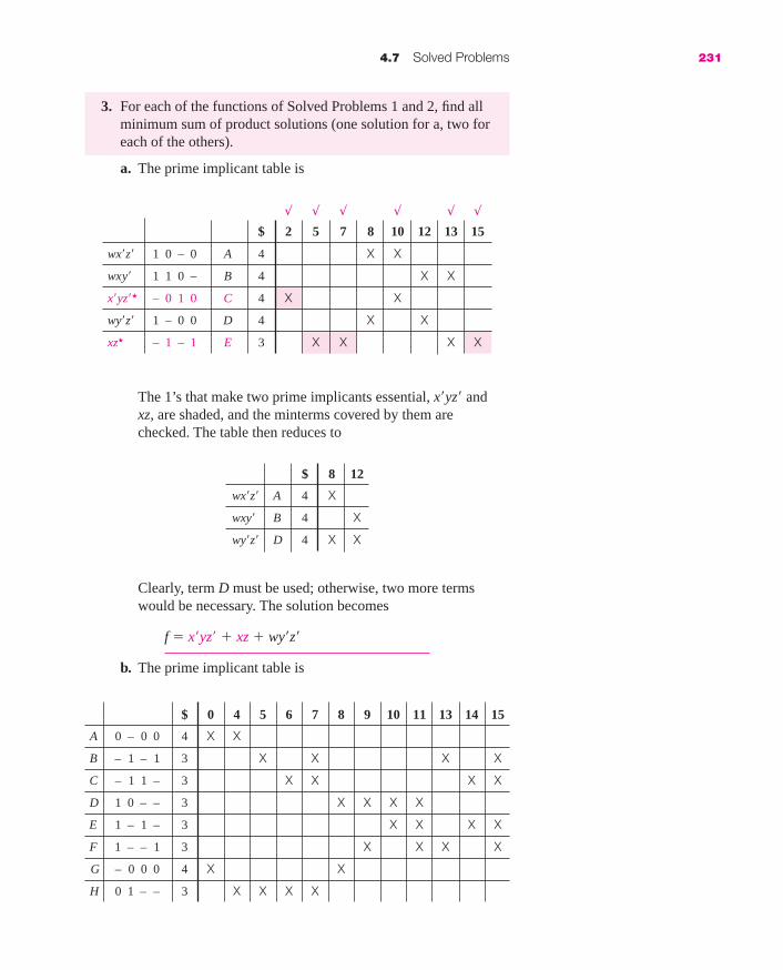
3. For each of the functions of Solved Problems 1 and 2, find allminimum sum of product solutions (one solution for a, two foreach of the others).
a. The prime implicant table is
4.7 Solved Problems 231
√ √ √ √ √ √
$ 2 5 7 8 10 12 13 15
wx�z� 1 0 – 0 A 4 X X
wxy� 1 1 0 – B 4 X X
x�yz�★ – 0 1 0 C 4 X X
wy�z� 1 – 0 0 D 4 X X
xz★ – 1 – 1 E 3 X X X X
$ 8 12
wx�z� A 4 X
wxy� B 4 X
wy�z� D 4 X X
The 1’s that make two prime implicants essential, x�yz� andxz, are shaded, and the minterms covered by them arechecked. The table then reduces to
Clearly, term D must be used; otherwise, two more termswould be necessary. The solution becomes
f � x�yz� � xz � wy�z�
b. The prime implicant table is
$ 0 4 5 6 7 8 9 10 11 13 14 15
A 0 – 0 0 4 X X
B – 1 – 1 3 X X X X
C – 1 1 – 3 X X X X
D 1 0 – – 3 X X X X
E 1 – 1 – 3 X X X X
F 1 – – 1 3 X X X X
G – 0 0 0 4 X X
H 0 1 – – 3 X X X X
mar91647_c04_201_248.qxd 11/5/08 10:40 AM Page 231

There are no essential prime implicants. The starting pointshould be one of the columns in which there are onlytwo X’s. We will choose minterm 5, since both terms willcover four 1’s (but we could have used minterm 0, 4, 5, 6, 8,9, 10, 13, or 14). We will first try prime implicant B; thenwe will try prime implicant H. If we choose B, the tablereduces to
232 Chapter 4 Function Minimization Algorithms
Row F is dominated by row D. If row D is chosen, the tablereduces to
$ 0 4 6 14
A 0 – 0 0 4 X X
C – 1 1 – 3 X X
E 1 – 1 – 3 X
G – 0 0 0 4 X
H 0 1 – – 3 X X
At this point, the only way to cover the function with twoterms is to choose A and C, giving a solution of
f � bd � ab� � a�c�d� � bc
Notice that if the dominated term F had been choseninstead of D, three additional terms would be required tocover the function, since minterms 8 and 10 are not coveredby F.
√ √ √ √$ 0 4 6 8 9 10 11 14
A 0 – 0 0 4 X X
C – 1 1 – 3 X X
D 1 0 – –★ 3 X X X X
E 1 – 1 – 3 X X X
F 1 – – 1 3 X X
G – 0 0 0 4 X X
H 0 1 – – 3 X X
mar91647_c04_201_248.qxd 11/5/08 3:38 PM Page 232

Now, we must consider what happens if we choose termH instead of B. The resulting table is
4.7 Solved Problems 233
√ √ √ √ √ √
$ 0 8 9 10 11 13 14 15
A 0 – 0 0 4 X
B – 1 – 1 3 X X
C – 1 1 – 3 X X
D 1 0 – – 3 X X X X
E 1 – 1 –★ 3 X X X X
F 1 – – 1 3 X X X X
G – 0 0 0★ 4 X X
√ √ √ √$ 1 3 5 6 7 13 14
0 – – 1★ A 3 X X X X
1 – – 0 B 3 X
– 1 0 1 C 4 X X
– 1 1 0 D 4 X X
1 1 0 – E 4 X
0 1 1 – F 4 X X
Prime implicant A is dominated by G, and C is dominated byE. Eliminating them, we must choose G and E, leaving onlyminterms 9 and 13 uncovered. They can both be covered byterm F. No other solution (that used H) requires as few asfour terms (even those using one of the dominated terms, Aor C). The resulting function, the second equally goodsolution, is
f � a�b � ac � b�c�d� � ad
c. The prime implicant table is
Note that there are no columns for the don’t cares; they do notneed to be covered. There is one essential prime implicant,A(W�Z), and the table can then be reduced to
mar91647_c04_201_248.qxd 11/5/08 10:40 AM Page 233

234 Chapter 4 Function Minimization Algorithms
√ √ √ √ √ √ √ √ √ √0 2 4 5 6 7 8 9 10 11 13 15 21 23 26 28 29 30 31
– 1 0 1 0 A 4 X X
1 1 – 1 0 B 4 X X
0 0 – – 0 C 3 X X X X
0 – 0 – 0 D 3 X X X X
0 0 1 – – E 3 X X X X
0 1 0 – – F 3 X X X X
0 1 – – 1 G 3 X X X X
1 1 1 – – H★ 3 X X X X
– – 1 – 1 J★ 2 X X X X X X X X
A study of the reduced table reveals that row D must bechosen; otherwise, it would take both terms B and F to coverminterms 6 and 14. That leaves us two choices to concludethe cover, C or E. Thus, the two solutions to the problem are
F � W�Z � XYZ� � XY�Z
F � W�Z � XYZ� � WXY�
d. The prime implicant table is
0 2 4 6 8 9 10 11 26
– 1 0 1 0 A 4 X X
1 1 – 1 0 B 4 X
0 0 – – 0 C 3 X X X X
0 – 0 – 0 D 3 X X X X
0 0 1 – – E 3 X X
0 1 0 – – F 3 X X X X
0 1 – – 1 G 3 X X
The two essential prime implicants are H and J. The table isthen reduced to
$ 6 13 14
1 – – 0 B 3 X
– 1 0 1 C 4 X
– 1 1 0 D 4 X X
1 1 0 – E 4 X
0 1 1 – F 4 X
mar91647_c04_201_248.qxd 11/5/08 10:40 AM Page 234

4.7 Solved Problems 235
At this point, there are nine minterms left to be covered. EitherA or B must be used for m26. C and F must be used to cover theremaining 1’s, producing the solutions
f � abc � ce � a�b�e� � a�bc� � bc�de�� abc � ce � a�b�e� � a�bc� � abde'
4. For each of the sets of functions, find all terms that may be usedin a minimum two-level AND/OR gate (or NAND gate) solutionusing the Quine-McCluskey method.
a. f(a, b, c, d) � �m(0, 1, 2, 3, 5, 7, 8, 10, 11, 13)g(a, b, c, d) � �m(0, 2, 5, 8, 10, 11, 13, 15)
b. f(w, x, y, z) � �m(5, 7, 9, 11, 13, 15)g(w, x, y, z) � �m(1, 5, 7, 9, 10, 11, 14)
c. f(a, b, c, d) � �m(0, 3, 5, 7) � �d(10, 11, 12, 13, 14, 15)g(a, b, c, d) � �m(0, 5, 6, 7, 8) � �d(10, 11, 12, 13, 14, 15)
d. f(a, b, c, d) � �m(0, 2, 3, 8, 9, 10, 11, 12, 13, 15)g(a, b, c, d) � �m(3, 5, 7, 12, 13, 15)h(a, b, c, d) � �m(0, 2, 3, 4, 6, 8, 10, 14)
a. We first form a column of minterms, organized by the numberof 1’s in each term. We then produce a second column ofthree-literal terms and a third of two-literal terms.
0 0 0 0 – – √ 0 0 0 – – 0 √ 0 0 – – – 0--------------- 0 0 – 0 – – √ – 0 – 0 – –0 0 0 1 – 0 √ – 0 0 0 – – √ ---------------0 0 1 0 – – √ --------------- 0 – – 1 – 01 0 0 0 – – √ 0 0 – 1 – 0 √ – 0 1 – – 0--------------- 0 – 0 1 – 0 √0 0 1 1 – 0 √ 0 0 1 – – 0 √0 1 0 1 – – √ – 0 1 0 – – √1 0 1 0 – – √ 1 0 – 0 – – √--------------- ---------------0 1 1 1 – 0 √ 0 – 1 1 – 0 √
1 0 1 1 – – √ – 0 1 1 – 0 √1 1 0 1 – – √ 0 1 – 1 – 0 √--------------- – 1 0 1 – –1 1 1 1 0 – √ 1 0 1 – – –
---------------1 – 1 1 0 –1 1 – 1 0 –
The unshared prime implicants of f are a�b�, a�d, and b�c; thoseof g are acd and abd. The shared terms are b�d�, bc�d, and ab�c.
mar91647_c04_201_248.qxd 11/5/08 10:40 AM Page 235

b.0 0 0 1 0 – √ 0 – 0 1 0 – – 1 – 1 – 0
--------------- – 0 0 1 0 – 1 – – 1 – 0
0 1 0 1 – – √ ---------------
1 0 0 1 – – √ 0 1 – 1 – –
1 0 1 0 0 – √ – 1 0 1 – 0 √
--------------- 1 0 – 1 – –
0 1 1 1 – – √ 1 – 0 1 – 0 √
1 0 1 1 – – √ 1 0 1 – 0 –
1 1 0 1 – 0 √ 1 – 1 0 0 –
1 1 1 0 0 – √ ---------------
--------------- – 1 1 1 – 0 √
1 1 1 1 – 0 √ 1 – 1 1 – 0 √
1 1 – 1 – 0 √
The prime implicants of f are xz and wz; those of g are w�y�z,x�y�z, wx�y, and wyz�. The terms that can be shared are w�xzand wx�z.
c. We must include all of the don’t cares
0 0 0 0 – – – 0 0 0 0 – 1 – – 0 0 –
--------------- --------------- ---------------
1 0 0 0 0 – √ 1 0 – 0 0 – √ – – 1 1 – 0
--------------- 1 – 0 0 0 – √ – 1 – 1 – –
0 0 1 1 – 0 √ --------------- – 1 1 – 0 –
0 1 0 1 – – √ 0 – 1 1 – 0 √ 1 – 1 – – –
0 1 1 0 0 – √ – 0 1 1 – 0 √ 1 1 – – – –
1 0 1 0 – – √ 0 1 – 1 – – √
1 1 0 0 – – √ – 1 0 1 – – √
--------------- 0 1 1 – 0 – √
0 1 1 1 – – √ – 1 1 0 0 – √
1 0 1 1 – – √ 1 0 1 – – – √
1 1 0 1 – – √ 1 – 1 0 – – √
1 1 1 0 – – √ 1 1 0 – – – √
--------------- 1 1 – 0 – – √
1 1 1 1 – – √ ---------------
– 1 1 1 – – √
1 – 1 1 – – √
1 1 – 1 – – √
1 1 1 – – – √
236 Chapter 4 Function Minimization Algorithms
mar91647_c04_201_248.qxd 11/5/08 10:40 AM Page 236

4.7 Solved Problems 237
The unshared prime implicant of f is cd; those of g areb�c�d�, ad�, and bc. The shared terms are a�b�c�d�, bd, ac,and ab.
d. The tag has three terms
0 0 0 0 – 0 – √ 0 0 – 0 – 0 – √ 0 – – 0 0 0 –
----------------- 0 – 0 0 0 0 – √ – 0 – 0 – 0 –
0 0 1 0 – 0 – √ – 0 0 0 – 0 – √ -----------------
0 1 0 0 0 0 – √ ----------------- – 0 1 – – 0 0
1 0 0 0 – 0 – √ 0 0 1 – – 0 – – – 1 0 0 0 –
----------------- 0 – 1 0 0 0 – √ 1 0 – – – 0 0
0 0 1 1 – – – – 0 1 0 – 0 – √ 1 – 0 – – 0 0
0 1 0 1 0 – 0 √ 0 1 – 0 0 0 – √ -----------------
0 1 1 0 0 0 – √ 1 0 0 – – 0 0 √ – 1 – 1 0 – 0
1 0 0 1 – 0 0 √ 1 0 – 0 – 0 – √ 1 – – 1 – 0 0
1 0 1 0 – 0 – √ 1 – 0 0 – 0 0 √
1 1 0 0 – – 0 √ -----------------
----------------- 0 – 1 1 0 – 0
0 1 1 1 0 – 0 √ – 0 1 1 – 0 0 √
1 0 1 1 – 0 0 √ 0 1 – 1 0 – 0 √
1 1 0 1 – – 0 √ – 1 0 1 0 – 0 √
1 1 1 0 0 0 – √ – 1 1 0 0 0 – √
----------------- 1 0 – 1 – 0 0 √
1 1 1 1 – – 0 √ 1 – 0 1 – 0 0 √
1 0 1 – – 0 0 √
1 – 1 0 0 0 – √
1 1 0 – – – 0
-----------------
– 1 1 1 0 – 0 √
1 – 1 1 – 0 0 √
1 1 – 1 – – 0
The unshared prime implicants of f are b�c, ab�, ac�, and ad;those of g are a�bc and bd; those of h are a�d� and cd�. Termsshared by f and g are abc� and abd; those shared by f and hare a�b�c and b�d�; the one shared by all three functionsis a�b�cd.
5. Repeat Solved Problem 4 using iterated consensus.
mar91647_c04_201_248.qxd 11/5/08 10:40 AM Page 237

We will start by finding all of the prime implicants of theproduct, fg, and then those that are prime implicants of theindividual functions but not of the product. (Of course, wewill add the appropriate tag section, – if it is included in thefunction, 0 if it is not.)
A – 0 – 0 – –
B 1 0 1 – – –
C – 1 0 1 – –
D 0 0 – – – 0
E 0 – – 1 – 0
F 1 1 – 1 0 –
G 1 – 1 1 0 –
After “completing” the list, it is a good idea to try theconsensus of all pairs of terms, in case we missed one. In thiscase, we did.
H – 0 1 – – 0 D ¢ B
Note that in trying the consensus, there is no need to take theconsensus of F or G with D or E (or H) since the tag would be0 0, indicating that the term is in neither function.
The unshared prime implicants of f are a�b�, a�d, andb�c; those of g are abd and acd. The terms that can be sharedare b�d�, ab�c, and bc�d.
b. We will solve this problem by starting with minterms andfinding all of the prime implicants.
238 Chapter 4 Function Minimization Algorithms
a. The maps of f, g, and fg are shown below
00 01 11 10
00
01
11
10
a b
c d
111
1
1
11
f g f g
1 1
1
00 01 11 10
00
01
11
10
a b
c d
11
11
11
1 1
00 01 11 10
00
01
11
10
a b
c d
1 1
1 1
1 1
1
mar91647_c04_201_248.qxd 11/5/08 10:40 AM Page 238

1 0 0 0 1 0 – A 0 – 0 1 0 – 5 ¢ 1 � 1
5 0 1 0 1 – – B 0 1 – 1 – – 7 ¢ 5 � 7, 5
7 0 1 1 1 – – C 1 0 1 – 0 – 11 ¢ 10 � 10
9 1 0 0 1 – – D 1 0 – 1 – – 11 ¢ 9 � 11, 9
10 1 0 1 0 0 – E 1 1 – 1 – 0 15 ¢ 13 � 15, 13
11 1 0 1 1 – – F 1 – 1 0 0 – C ¢ 14 � 14
13 1 1 0 1 – 0 G – 0 0 1 0 – D ¢ A
14 1 1 1 0 0 – H 1 – – 1 – 0 E ¢ D � E
15 1 1 1 1 – 0 J – 1 – 1 – 0 H ¢ B
Each of the new terms that is created by consensus is shown;all of the original terms and one of the groups of 2 areincluded in a larger prime implicant.
The unshared prime implicants of f are wz and xz; thoseof g are w�y�z, wx�y, wyz�, and x�y�z. The product terms thatcan be shared are w�xz and wx�z.
c. In finding the prime implicants, we must treat all don’t caresas 1’s. We first map f, g, and fg, converting all X’s to 1’s to findthe prime implicants. (Once again, it is a good idea to checkthat none have been missed by using the iterated consensusalgorithm on the result.)
4.7 Solved Problems 239
The unshared prime implicant of f is cd; those of g are bc,ad�, and b�c�d�. The shared terms are a�b�c�d�, bd, ab,and ac.
d. We first map the functions and all the products of pairs offunctions. (We do not need a separate map for fgh, since itequals gh.)
00 01 11 10
00
01
11
10
a b
c d
1
1 1
1
f g f g
1 1 1 1
11
00 01 11 10
00
01
11
10
a b
c d
1
11 1
111
1
1 1 1
00 01 11 10
00
01
11
10
a b
c d
1
1 11
1 1
1
11
mar91647_c04_201_248.qxd 11/5/08 10:40 AM Page 239
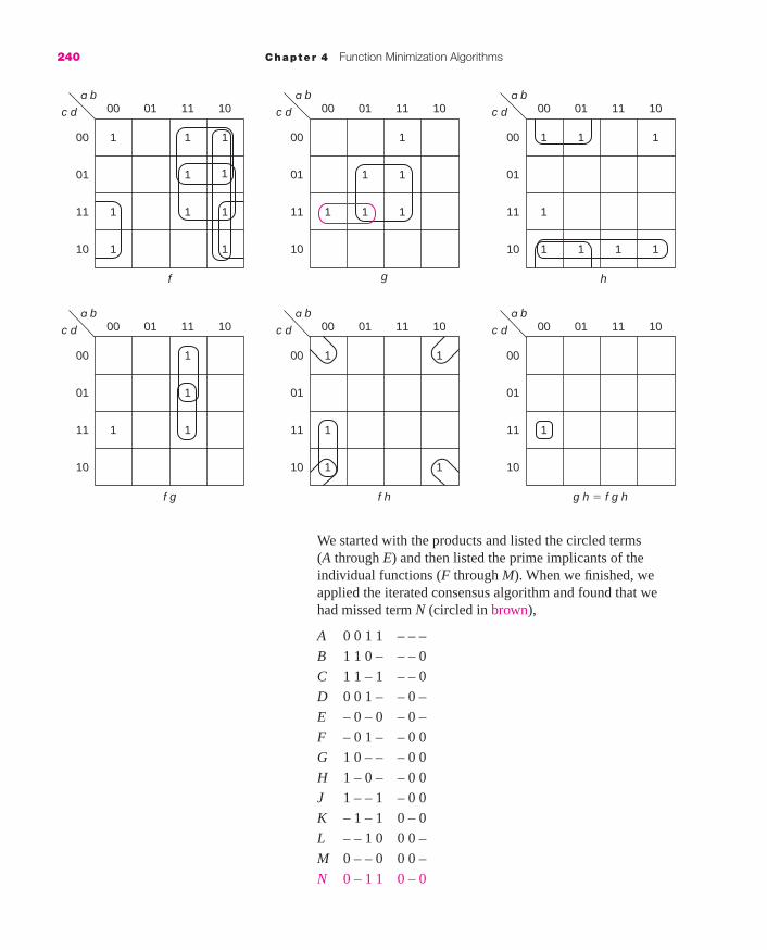
We started with the products and listed the circled terms(A through E) and then listed the prime implicants of theindividual functions (F through M). When we finished, weapplied the iterated consensus algorithm and found that wehad missed term N (circled in brown),
A 0 0 1 1 – – –
B 1 1 0 – – – 0
C 1 1 – 1 – – 0
D 0 0 1 – – 0 –
E – 0 – 0 – 0 –
F – 0 1 – – 0 0
G 1 0 – – – 0 0
H 1 – 0 – – 0 0
J 1 – – 1 – 0 0
K – 1 – 1 0 – 0
L – – 1 0 0 0 –
M 0 – – 0 0 0 –
N 0 – 1 1 0 – 0
240 Chapter 4 Function Minimization Algorithms
00 01 11 10
00
01
11
10
a b
c d
1
1
1
1
f g h
1 1 1
1
00 01 11 10
00
01
11
10
a b
c d
11
1
1
1
00 01 11 10
00
01
11
10
a b
c d
1
1
11
1111
00 01 11 10
00
01
11
10
a b
c d
1
1
f g f h g h � f g h
1 1
00 01 11 10
00
01
11
10
a b
c d
1 1
1
1
1
00 01 11 10
00
01
11
10
a b
c d
1
1
1 1
mar91647_c04_201_248.qxd 11/5/08 10:40 AM Page 240

f g
√ √ √ √ √ √ √ √ √ √ √ √ √ √ √0 1 2 3 5 7 8 10 11 13 0 2 5 8 10 11 13 15
– 0 – 0★ 3 A X X X X X X X X
1 0 1 – 4 B X X X X
– 1 0 1★ 4 C X X X X
0 0 – – 3 D X X X X
0 – – 1★ 3 E X X X X
1 1 – 1 4 F X X
1 – 1 1 4 G X X
– 0 1 – 3 H X X X X
4.7 Solved Problems 241
Terms A and C are essential prime implicants of both f and g,and E is an essential prime implicant of f. The reduced tablethus becomes
Term G completes the cover of g and term H would thenbe used for f since it is less expensive than B. The otheroption, using B for both f and g, and then using either F orG to cover m15 in g, would cost an extra input. The solution
6. For each of the sets of functions of Solved Problems 4 and 5, find a set of minimum sum of products expressions,corresponding to a two-level AND/OR gate (or NAND gate)system (a. 1 solution, b. 6 solutions, c. 2 solutions,d. 2 solutions).
a. The prime implicant table is
f g
11 11 15
1 0 1 – 4 B X X
0 0 – – 3 D
1 1 – 1 4 F X
1 – 1 1 4 G X X
– 0 1 – 3 H X
mar91647_c04_201_248.qxd 11/5/08 10:40 AM Page 241

The two essential prime implicants of g, w�xz and wyz�, areshown. The table is then reduced (and the cost of B is made 1,since the AND gate was already built).
242 Chapter 4 Function Minimization Algorithms
We have two sharing possibilities. We could share B, using itwith G to cover f. Then, we have three choices for g: A + D,F + D, and F + C, costing 1 for B, 3 for G, and 8 for any of thepair of terms covering g, costing a total of 12. If not, we couldchoose D to share. In that case, we could cover f with onemore term, H, and cover g with either A or F. That would cost5 for D, 3 for H, and 4 for A or F, also a total of 12.
thus becomes
f � b�d� � bc�d � a�d � b�c
g � b�d� � bc�d � acd
b. The prime implicant table is
f g
√ √ √ √5 7 9 11 13 15 1 5 7 9 10 11 14
0 – 0 1 A 4 X X
0 1 – 1★ B 4 X X X X
1 0 1 – C 4 X X
1 0 – 1 D 4 X X X X
1 – 1 0★ E 4 X X
– 0 0 1 F 4 X X
1 – – 1 G 3 X X X X
– 1 – 1 H 3 X X X X
f g
5 7 9 11 13 15 1 9 11
0 – 0 1 A 4 X
0 1 – 1 B 1 X X
1 0 1 – C 4 X
1 0 – 1 D 4 X X X X
– 0 0 1 F 4 X X
1 – – 1 G 3 X X X X
– 1 – 1 H 3 X X X X
mar91647_c04_201_248.qxd 11/5/08 10:40 AM Page 242

The three solutions that share B, w�x z, are
f1 � w�xz � wzg1 � w�xz � wyz� � w�y�z � wx�zg2 � w�xz � wyz� � wx�y � x�y�zg3 � w�xz � wyz� � wx�z � x�y�z
The two that share D, wx�z, are
f2 � wx�z � xzg4 � w�xz � wyz� � wx�z � w�y�zg5 � w�xz � wyz� � wx�z � x�y�z
c. This produces the following prime implicant table.
4.7 Solved Problems 243
Notice that prime implicants A and C cover no minterms;they are both groups of four don’t cares. The function f iscovered by essential prime implicants; only minterms 0 and8 of g are left. The reduced prime implicant table (for g)becomes
f g
√ √ √ √ √ √ √0 3 5 7 0 5 6 7 8
1 1 – – A 3
– 1 – 1★ B 3 X X X X
1 – 1 – C 3
0 0 0 0★ D 5 X X
– – 1 1★ E 3 X X
– 0 0 0 F 4 X X
– 1 1 –★ G 3 X X
1 – – 0 H 3 X
g
0 8
0 0 0 0 D 1 X
– 0 0 0 F 4 X X
1 – – 0 H 3 X
There are two equally good solutions. Prime implicant Fcovers both minterms, but requires one AND gate and fourinputs. Prime implicant D was an essential prime implicant of
mar91647_c04_201_248.qxd 11/5/08 10:40 AM Page 243

f and thus does not require a new AND gate and only one gateinput. Thus, D and H also produce a solution that requires onenew gate and four inputs. The two solutions are
f � bd � a�b�c�d� � cd
and
g1 � bd � bc � b�c�d�
or
g2 � bd � bc � a�b�c�d� � ad�
d. When we map the various products and find all of the primeimplicants, we come up with the following prime implicanttable. Note that because of its size, we have broken it intotwo parts. We show all of the prime implicants in each part of the table, although some of the rows are empty in onepart of the table. After finding essential prime implicants,we will be able to combine the tables and complete theproblem.
244 Chapter 4 Function Minimization Algorithms
f
√ √ √ √0 2 3 8 9 10 11 12 13 15
0 0 1 1 A 5 X
1 1 0 – B 4 X X
1 1 – 1 C 4 X X
– 0 – 0★ D 3 X X X X
0 0 1 – E 4 X X
1 0 – – F 3 X X X X
1 – 0 – G 3 X X X X
1 – – 1 H 3 X X X X
– 0 1 – J 3 X X X X
– 1 – 1 K 3
0 – 1 1 L 4
0 – – 0 M 3
– – 1 0 N 3
mar91647_c04_201_248.qxd 11/5/08 10:40 AM Page 244
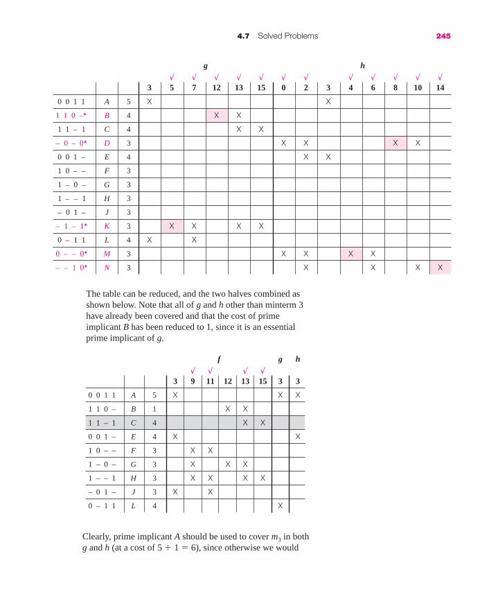
4.7 Solved Problems 245
g h
√ √ √ √ √ √ √ √ √ √ √ √3 5 7 12 13 15 0 2 3 4 6 8 10 14
0 0 1 1 A 5 X X
1 1 0 –★ B 4 X X
1 1 – 1 C 4 X X
– 0 – 0★ D 3 X X X X
0 0 1 – E 4 X X
1 0 – – F 3
1 – 0 – G 3
1 – – 1 H 3
– 0 1 – J 3
– 1 – 1★ K 3 X X X X
0 – 1 1 L 4 X X
0 – – 0★ M 3 X X X X
– – 1 0★ N 3 X X X X
The table can be reduced, and the two halves combined asshown below. Note that all of g and h other than minterm 3have already been covered and that the cost of primeimplicant B has been reduced to 1, since it is an essentialprime implicant of g.
f g h
√ √ √ √3 9 11 12 13 15 3 3
0 0 1 1 A 5 X X X
1 1 0 – B 1 X X
1 1 – 1 C 4 X X
0 0 1 – E 4 X X
1 0 – – F 3 X X
1 – 0 – G 3 X X X
1 – – 1 H 3 X X X X
– 0 1 – J 3 X X
0 – 1 1 L 4 X
Clearly, prime implicant A should be used to cover m3 in bothg and h (at a cost of 5 � 1 � 6), since otherwise we would
mar91647_c04_201_248.qxd 11/5/08 10:40 AM Page 245

need both E and L at a cost of 8. For f, we can eliminate primeimplicant C, since that row is dominated by row H and costsmore. That requires us to choose H to cover m15. Once H ischosen, all that remains to be covered are m3 and m12, whichcan be covered by A and B (respectively), each at a cost of 1.(J or G could have been used, but they would cost 3 each.) Thefinal functions are
f � b�d� � ad � a�b�cd � abc�
g � abc� � bd � a�b�cd
h � b�d� � a�d� � cd� � a�b�cd
4.8 EXERCISES*
1. For each of the following functions, find all prime implicants usingthe Quine-McCluskey method.
a. f(a, b, c) � �m(1, 2, 3, 6, 7)★ b. g(w, x, y) � �m(0, 1, 5, 6, 7)
c. g(w, x, y, z) � �m(2, 3, 6, 7, 8, 10, 11, 12, 13, 15)★ d. h(p, q, r, s) � �m(0, 2, 3, 4, 5, 8, 11, 12, 13, 14, 15)
e. f(a, b, c, d) � �m(5, 7, 9, 11, 13, 14) � �d(2, 6, 10, 12, 15)★ f. f(a, b, c, d) � �m(0, 2, 4, 5, 6, 7, 8, 9, 10, 14) � �d(3, 13)
g. G(V, W, X, Y, Z) � �m(0, 1, 4, 5, 8, 9, 10, 15, 16, 18, 19,20, 24, 26, 28, 31)
★ h. H(V, W, X, Y, Z) � �m(0, 1, 2, 3, 5, 7, 10, 11, 14, 15,16, 18, 24, 25, 28, 29, 31)
2. For the functions of Exercise 1, find all prime implicants usingiterated consensus.
3. For the functions of Exercises 1 and 2, find all minimum sum ofproducts expressions (b. 2 solutions, c. 2 solutions, d. 4 solutions,e. 4 solutions, f. 3 solutions, h. 2 solutions, all others, 1 solution).
4. For the following sets of functions, find all product terms thatcould be used in a minimum two-level AND/OR system using theQuine-McCluskey algorithm.
a. f(a, b, c, d) � �m(5, 8, 9, 12, 13, 14)
g(a, b, c, d) � �m(1, 3, 5, 8, 9, 10)★ b. F(W, X, Y, Z) � �m(1, 5, 7, 8, 10, 11, 12, 14, 15)
G(W, X, Y, Z) � �m(0, 1, 4, 6, 7, 8, 12)
246 Chapter 4 Function Minimization Algorithms
*Each of the functions and sets of functions was included in the exercises of Chapter 3.Other exercises from that chapter could also be used here.
EX
ER
CIS
ES
mar91647_c04_201_248.qxd 11/5/08 10:40 AM Page 246

4.9 Chapter 4 Test 247
c. f(a, b, c, d) � �m(1, 3, 5, 7, 8, 9, 10)
g(a, b, c, d) � �m(0, 2, 4, 5, 6, 8, 10, 11, 12)
h(a, b, c, d) � �m(1, 2, 3, 5, 7, 10, 12, 13, 14, 15)★ d. f(a, b, c, d) � �m(0, 3, 4, 5, 7, 8, 12, 13, 15)
g(a, b, c, d) � �m(1, 5, 7, 8, 9, 10, 11, 13, 14, 15)
h(a, b, c, d) � �m(1, 2, 4, 5, 7, 10, 13, 14, 15)
5. For each of the sets of functions of Solved Problem 4, find allproduct terms that could be used in a minimum two-level AND/ORsystem using iterated consensus.
6. For each of the sets of functions of Solved Problems 4 and 5, find aset of minimum sum of products expressions, corresponding to atwo-level AND/OR gate (or NAND gate) system.
a. 3 solutions, 8 gates, 25 inputs
b. 8 gates, 23 inputs
c. 2 solutions, 12 gates, 33 inputs
d. 2 solutions, 11 gates, 33 inputs
4.9 CHAPTER 4 TEST (50 MINUTES)*
1. For the following function, find all of the prime implicants using
a. the Quine-McCluskey method.
b. iterated consensus.
f(w, x, y, z) � �m(0, 2, 3, 6, 8, 12, 15) � �d (1, 5)
2. For the following function,
g(a, b, c, d) � �m(3, 4, 5, 6, 7, 8, 9, 12, 13, 14)
we have found the complete list of prime implicants
a�cd bd'
a�b ac'
bc'
Find both of the minimum sum of products solutions.
3. For the following set of functions, find all terms that can be used ina minimum two-level AND/OR system using
a. the Quine-McCluskey method.
b. iterated consensus.
f(w, x, y, z) � �m(1, 2, 5, 7, 10, 11, 13, 15)
g(w, x, y, z) � �m(0, 2, 3, 4, 5, 7, 8, 10, 11, 12)
*The timing assumes that the student will solve either 1a. or 1b. and either 3a. or 3b.
EX
ER
CIS
ES
CH
AP
TE
R T
ES
T
mar91647_c04_201_248.qxd 11/5/08 3:38 PM Page 247

248 Chapter 4 Function Minimization Algorithms
4. For the following set of functions,
f(a, b, c, d) � �m(2, 3, 4, 6, 7) � �d(0, 1, 14, 15)g(a, b, c, d) � �m(2, 3, 5, 7, 8, 10, 13) � �d(0, 1, 14, 15)
We found the possible shared terms: a�b�, a�cd, bcd, abc.
Other prime implicants of f are a�d�, a�c, bc.
Other prime implicants of g are a�d, b�d�, bd, acd�.
Find a set of minimum sum of products expressions, correspondingto a two-level AND/OR gate (or NAND gate) system.
CH
AP
TE
R T
ES
T
mar91647_c04_201_248.qxd 11/5/08 10:40 AM Page 248

249
C H A P T E R
5Designing Combinational Systems
Until now, we have concentrated on rather small systems—mostlysystems with five or fewer inputs and three or fewer outputs. Inthis chapter, we want to expand our horizons. Large systems are
usually designed by breaking them up into smaller subsystems. Indeed,these subsystems may need to be broken down still further.
In this chapter, we will first look at systems that consist of a numberof identical blocks. (These are sometimes referred to as iterative systems.)Adders and other arithmetic functions are examples of this type of system.
Because signals in large systems pass through many layers of logic,the small delay encountered as a signal passes through a single gate addsup. We will use the design of a multibit adder to illustrate this.
Next, we will look at some common types of circuit—the binarydecoder and encoder, and the multiplexer. Each of these have manyapplications in digital system design and are available commercially in avariety of forms.
Another class of circuits used in the design of medium- and large-size systems is gate arrays, sometimes referred to as programmablelogic devices (PLDs). As we will discuss in Chapter 7, some PLDs alsocontain memory. Gate arrays consist of a set of AND gates and a set ofOR gates connected to form SOP expressions. The basic structure isstandard; some of the connections can be specified by the user. Gatearrays are commonly available in three forms: read only memory (ROM),programmable logic array (PLA), and programmable array logic (PAL).
We will also look at issues of testing and simulation of combina-tional circuits.
We will then look at the design of a decimal adder and a driver for aseven-segment display. We will use a variety of the techniques of thischapter and Chapter 3 in these designs. A large number of exercises(Exercises 20–25) fall into this category.
mar91647_c05a_249_285.qxd 11/14/08 12:16 PM Page 249

250 Chapter 5 Designing Combinational Systems
5.1 ITERATIVE SYSTEMSWe will first look at adders as an example of a system that can be imple-mented with multiple copies of a smaller circuit. We will use the adder toillustrate the issue of delay in multiple-level circuits and then discussother iterative circuits.
When we add two numbers by hand, we add the two least significantdigits (plus possibly a carry-in) to produce one bit of the sum and a carry to the next bit. Such a one-bit adder (referred to as a full adder) isdefined as CE3 and was designed with NAND gates in Example 2.34 (Section 2.8). If we wish to build an n-bit adder, we need only connect nof these. A 4-bit version is shown in Figure 5.1.
FullAdder
FullAdder
FullAdder
FullAdder
a4 b4 a3 b3 b2a2
c1
c1 cina1
s1s2s3s4cout
b1
Figure 5.1 A 4-bit adder.
A
F
X
B
C
(a) (b)
A
B
X
C
F
1 2 4 53
5.1.1 Delay in Combinational Logic Circuits
When the input to a gate changes, the output of that gate does not changeinstantaneously, but there is a small delay, �. If the output of one gate isused as the input to another, the delays add. A block diagram of a simplecircuit is shown in Figure 5.2a and the timing diagram associated with itin Figure 5.2b.
Figure 5.2 Illustration of gate delay.
mar91647_c05a_249_285.qxd 11/14/08 12:16 PM Page 250

When a change in C causes F to change, F changes one delay time,�, later, as shown at time 1. If A or B changes, then point X changes onedelay time later, and F changes one time after that, as indicated at time 2.At time 3, a change in C does not cause a change in F, and at time 4, achange in B causes a change in X, but not the output. Finally, at time 5,both B and C change simultaneously. The output F goes to 0 briefly whenthe change in C is recognized (� after the change in C), and then F returnsto 1 when the change in B is propagated (2� after the change in B). Thissituation is known as a hazard or a glitch.
The output is stable after the longest delay path. We are not usuallyinterested in the output until it is stable. In this case, that time is 2�. Asa more complex example of delay, we will consider the full adder, thesystem of CE3. It adds two 1-bit numbers and a carry input from the nextless significant digit and produces a sum bit and a carry out to the nextmore significant digit.
We will now look at the time it takes for the result of an addition tobe available at the two outputs of the full adder. We will assume that allinputs are available at the same time. Figure 5.3 repeats the adder circuitof Example 2.34 (from Section 2.8), with the delay (from when inputs aand b change) indicated at various points in the circuit. Of course, if twoinputs to a gate change at different times, the output may change as lateas � after the last input change.
As shown, the delay from the time inputs a or b change to the timethat the sum is available is 6� and to the time that the carry-out is avail-able is 5�. If a and b are established,* the delay from the carry-in to the
5.1 Iterative Systems 251
*All of the bits of the two multidigit numbers to be added are normally available at one time.Thus, after the least significant digit, all of the a’s and b’s are established before cin arrives.
a
b s
cin
cout
�
2�
3�
4�
5�
6�
5�
Figure 5.3 Delay through a 1-bit adder.
mar91647_c05a_249_285.qxd 11/14/08 12:16 PM Page 251

carry-out is only 2�, since cin passes through only two gates on the wayto cout, as shown in the brown path. This latter time is most critical, as wewill see shortly. (Also, the delay from carry-in to sum is 3�.)
We can build an n-bit adder with n copies of the full adder; as shownin Figure 5.1. The total time required is calculated as the delay from theinputs to cout (for the least significant bit) plus n � 2 times the delay fromcin to cout (for the middle full adders), plus the longer of the delay from cin
to cout or from cin to s (for the most significant bit). For the multileveladder, that equals 5� � 2(n � 2)� � 3� � (2n � 4)�. For a 64-bitadder, the delay would be 132�.
5.1.2 Adders
As indicated in the previous section, one approach to building an n-bitadder is to connect together n 1-bit adders. This is referred to as a carry-ripple adder. The time for the output of the adder to become stable maybe as large as (2n � 4)�. It does not always take that long for all the out-puts to be set, because, for any bit, if ai and bi are both 1, then a carry-outis always 1 (independent of the carry-in from lower order bits) and if ai
and bi are both 0, then a carry-out is always 0.To speed this up, several approaches have been attempted. One
approach is to implement a multibit adder with an SOP expression. Afterall, an n-bit adder (with a carry-in to the least significant bit) is just a 2n � 1 variable problem. In theory, we can construct a truth table for thatand get an SOP (or POS) expression.
The truth table for a 2-bit adder is shown in Table 5.1, where bit 1 isthe low order bit. This can be implemented by an SOP expression. The(five-variable) maps are shown in Map 5.1. The prime implicants are notcircled because that would make the map unreadably cluttered.
The minimum SOP expressions are
cout � a2b2 � a1b1a2 � a1b1b2 � cinb1b2 � cinb1a2 � cina1b2
� cina1a2
s2 � a1b1a2�b2� � a1b1a2b2 � cin� a1�a2�b2 � cin� a1�a2b2�
� cin� b1�a2�b2 � cin� b1�a2b2� � a1�b1�a2b2�
� a1�b1�a2�b2 � cinb1a2�b2� � cinb1a2b2
� cina1a2�b2� � cina1a2b2
s1 � cin� a1�b1 � cin� a1b1� � cina1�b1� � cina1b1
The equations are very complex, requiring 23 terms with 80 literals. Atwo-level solution would require a 12-input gate for s1. Clearly, we couldrepeat this process for a 3-bit or 4-bit adder, but the algebra gets verycomplex, and the number of terms increases drastically. (We do not haveseven- or nine-variable maps; other methods would work, although it
252 Chapter 5 Designing Combinational Systems
mar91647_c05a_249_285.qxd 11/14/08 12:16 PM Page 252

would be a lengthy process by hand.) We could also manipulate thealgebra to produce multilevel solutions with fewer large gates, but thatwould increase the delay. Another problem that we would encounter inthat implementation in the real world is that there is a limitation on thenumber of inputs (called fan-in) for a gate. Gates with 12 inputs may notbe practical or may encounter delays of greater than �.
For the 2-bit adder, cout can be implemented with two-level logic(with a maximum fan-in of seven). Thus, the delay from carry-in tocarry-out of every two bits is only 2� (other than the first 2 and the last2 bits) producing a total delay of
2� � 2(n�2 � 2)� � 3� � (n � 1)�
about half that of the previous solution.
5.1 Iterative Systems 253
Table 5.1 Two-bit adder truth table.
a2 b2 a1 b1 cin cout s2 s1
0 0 0 0 0 0 0 00 0 0 0 1 0 0 10 0 0 1 0 0 0 10 0 0 1 1 0 1 00 0 1 0 0 0 0 10 0 1 0 1 0 1 00 0 1 1 0 0 1 00 0 1 1 1 0 1 10 1 0 0 0 0 1 00 1 0 0 1 0 1 10 1 0 1 0 0 1 10 1 0 1 1 1 0 00 1 1 0 0 0 1 10 1 1 0 1 1 0 00 1 1 1 0 1 0 00 1 1 1 1 1 0 11 0 0 0 0 0 1 01 0 0 0 1 0 1 11 0 0 1 0 0 1 11 0 0 1 1 1 0 01 0 1 0 0 0 1 11 0 1 0 1 1 0 01 0 1 1 0 1 0 01 0 1 1 1 1 0 01 1 0 0 0 1 0 01 1 0 0 1 1 0 11 1 0 1 0 1 0 11 1 0 1 1 1 1 01 1 1 0 0 1 0 11 1 1 0 1 1 1 01 1 1 1 0 1 1 01 1 1 1 1 1 1 1
mar91647_c05a_249_285.qxd 11/14/08 12:16 PM Page 253

There have been some compromises, where the carry is imple-mented with a two-level circuit and the sum is a less complex multilevelcircuit. This only increases the delay by a few � (for the last sum), inde-pendent of n.
There are commercially available 4-bit adders: the 7483, 7483A,and 74283. Each is implemented differently, with a three-level circuit forthe carry-out. The 7483A and 74283 differ only in pin connections; each
254 Chapter 5 Designing Combinational Systems
00 01 11 10
00
01
11
10
1
1
1
1
00 01 11 10
00
01
11
10 1
1
11
1
1
1
1
1
1
1
1
00 01 11 10
00
01
11
10
1 1
1
1
00 01 11 10
00
01
11
10
1
11
1
1
1
1
1
00 01 11 10
00
01
11
10
1
1
1
00 01 11 10
00
01
11
10
11
1
1
1
1
1
1
11
1
1
1
1
1 1
1
cinb1
b2a1
cinb1
b2a1
cinb1
b2a1
cinb1
b2a1
cinb1
a2
a2
a2
s1
s2
cout
b2a1
cinb1
b2a1
0 1
0 1
0 1
Map 5.1 2-bit adder.
mar91647_c05a_249_285.qxd 11/14/08 12:16 PM Page 254
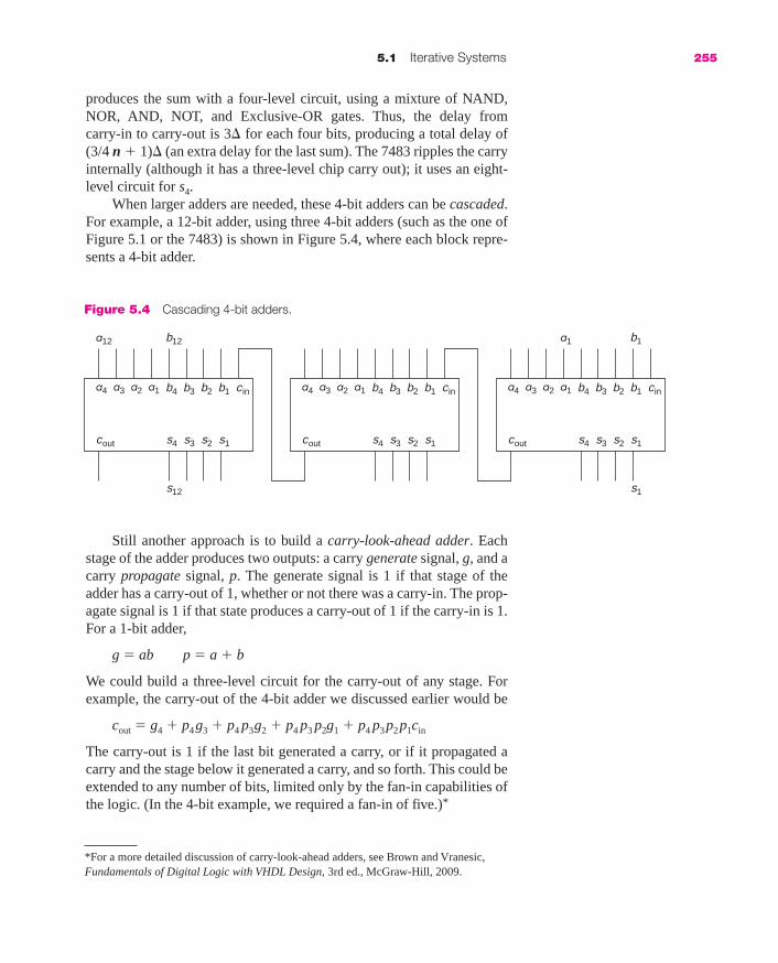
produces the sum with a four-level circuit, using a mixture of NAND,NOR, AND, NOT, and Exclusive-OR gates. Thus, the delay from carry-in to carry-out is 3� for each four bits, producing a total delay of(3/4 n � 1)� (an extra delay for the last sum). The 7483 ripples the carryinternally (although it has a three-level chip carry out); it uses an eight-level circuit for s4.
When larger adders are needed, these 4-bit adders can be cascaded.For example, a 12-bit adder, using three 4-bit adders (such as the one ofFigure 5.1 or the 7483) is shown in Figure 5.4, where each block repre-sents a 4-bit adder.
5.1 Iterative Systems 255
*For a more detailed discussion of carry-look-ahead adders, see Brown and Vranesic,Fundamentals of Digital Logic with VHDL Design, 3rd ed., McGraw-Hill, 2009.
Figure 5.4 Cascading 4-bit adders.
a4
cout
a3 a2 a1 b4
a12 b12
b3 b2 b1
s4
s12 s1
s3 s2 s1
cin a4
cout
a3 a2 a1 b4 b3 b2 b1
s4 s3 s2 s1
cin a4
cout
a3 a2 a1 b4 b3 b2 b1
a1 b1
s4 s3 s2 s1
cin
Still another approach is to build a carry-look-ahead adder. Eachstage of the adder produces two outputs: a carry generate signal, g, and acarry propagate signal, p. The generate signal is 1 if that stage of theadder has a carry-out of 1, whether or not there was a carry-in. The prop-agate signal is 1 if that state produces a carry-out of 1 if the carry-in is 1.For a 1-bit adder,
g � ab p � a � b
We could build a three-level circuit for the carry-out of any stage. Forexample, the carry-out of the 4-bit adder we discussed earlier would be
cout � g4 � p4g3 � p4 p3g2 � p4 p3 p2g1 � p4 p3p2p1cin
The carry-out is 1 if the last bit generated a carry, or if it propagated acarry and the stage below it generated a carry, and so forth. This could beextended to any number of bits, limited only by the fan-in capabilities ofthe logic. (In the 4-bit example, we required a fan-in of five.)*
mar91647_c05a_249_285.qxd 11/14/08 12:16 PM Page 255

5.1.3 Subtractors and Adder/Subtractors
To do subtraction, we could develop the truth table for a 1-bit full sub-tractor (See Solved Problem 3) and cascade as many of these as areneeded, producing a borrow-ripple subtractor.
Most of the time, when a subtractor is needed, an adder is needed aswell. In that case, we can take advantage of the approach to subtractionwe developed in Section 1.2.4. There, we complemented each bit of thesubtrahend and added 1.
To build such an adder/subtractor, we need a signal line that is 0 foraddition and 1 for subtraction. We will call that a�/s (short for add�/subtract).* Remembering that
1 � x � x� and 0 � x � x
we can now build the circuit of Figure 5.5, using the 4-bit adder we havealready designed. There needs to be an Exclusive-OR on each input. Thecarry-out from one stage is connected directly to the carry-in of the next.The bi of all stages are connected through Exclusive-OR gates enabledby a�/s.
256 Chapter 5 Designing Combinational Systems
a4
cout
a3 a2 a1 b4 b3 b2 b1
b4
b3
b2
b1
s4 s3 s2 s1
cina�/s
*This notation is quite common. The a� indicates that a 0 on this line calls for additionand the s implies that a 1 on this line calls for subtraction.
Figure 5.5 A 4-bit adder/subtractor.
5.1.4 Comparators
A common arithmetic requirement is to compare two numbers, produc-ing an indication if they are equal or if one is larger than the other. The
mar91647_c05a_249_285.qxd 11/14/08 12:16 PM Page 256

Exclusive-OR produces a 1 if the two inputs are unequal and a 0,otherwise. Multibit numbers are unequal if any of the input pairs areunequal. The circuit of Figure 5.6a shows a 4-bit comparator. The outputof the NOR is 1 if the numbers are equal. In Figure 5.6b, we accom-plished the same thing with Exclusive-NORs and an AND gate.
5.1 Iterative Systems 257
Figure 5.6 Two 4-bit comparators.
a4
a3
a2
a1
b4
b3
b2
b1
(a) Exclusive-OR
a � b
a4
a3
a2
a1
b4
b3
b2
b1
(b) Exclusive-NOR
a � b
These comparators can be extended to any number of bits.To build a 4-bit comparator that will indicate greater than and less
than, as well as equal to (for unsigned numbers), we recognize that, start-ing at the most significant bit (a4 and b4),
a �b if a4 � b4 or (a4 � b4 and a3 � b3) or (a4 � b4 and
a3 � b3 and a2 � b2) or (a4 � b4 and a3 � b3 and a2 � b2 and
a1 > b1)
a � b if a4 � b4 or (a4 � b4 and a3 � b3) or (a4 � b4 and
a3 � b3 and a2 � b2) or (a4 � b4 and a3 � b3 and a2 � b2 and
a1 � b1)
a � b if a4 � b4 and a3 � b3 and a2 � b2 and a1 � b1
This can, of course, be extended to any size, or 4-bit comparators can becascaded, passing on the three signals, greater than, less than, and equalto. A typical bit of such a comparator is shown in Figure 5.7.
The 7485 is a 4-bit comparator, with cascading inputs and outputs.Like the adder, the cascading signals go from lower order module tohigher order module (as opposed to the previous example). It thus com-putes the greater output as 1 if the a inputs to this module are greater thanthe b inputs or if they are equal and the cascading input is greater.
mar91647_c05a_249_285.qxd 11/14/08 12:16 PM Page 257

258 Chapter 5 Designing Combinational Systems
ba
�
�
�
�
�
�
Figure 5.7 Typical bit of a comparator.
*Although 4 inputs have 16 combinations, some decoders only have 10 outputs.
5.2 BINARY DECODERSA binary decoder is a device that, when activated, selects one of severaloutput lines, based on a coded input signal. Most commonly, the input isan n-bit binary number, and there are up to 2n output lines.* (Somedecoders have an enable signal that activates it; we will get to that shortly.)
The truth table for a two-input (four-output) decoder is shown inTable 5.2a. The inputs are treated as a binary number, and the outputselected is made active. In this example, the output is active high, that is,the active output is 1 and the inactive ones are 0. (We will use the termsactive high and active low (active value is 0) to refer both to inputs andoutputs.) This decoder just consists of an AND gate for each output, plusNOT gates to invert the inputs. (We assume only a and b are available,not their complements.) The block diagram is given in Figure 5.8a. Out-put 0 is just a�b�; output 1 is a�b; output 2 is ab�; and output 3 is ab. Eachoutput corresponds to one of the minterms for a two-variable function.
An active low output version of the decoder has one 0 correspondingto the input combination; the remaining outputs are 1. The circuit and thetruth table describing it are shown in Figure 5.8b and Table 5.2b. TheAND gates in the previous circuit are just replaced by NANDs.
Most decoders also have one or more enable inputs. When such aninput is active, the decoder behaves as described. When it is inactive, allof the outputs of the decoder are inactive. In most systems with a single
[SP 1, 2, 3, 4; EX 1, 2, 3, 4, 5, 6; LAB]
mar91647_c05a_249_285.qxd 11/14/08 12:16 PM Page 258

enable input (not just decoders), that input is active low. The truth table,a block diagram, and the circuit for an active high output decoder with anactive low enable input is shown in Figure 5.9. Note that the enable inputis inverted and connected to each AND gate. When EN� � 1, a 0 is on theinput to each AND gate, and, thus, all of the AND gate outputs are 0.When EN� � 0, the additional input (beyond those for the circuit withoutan enable) is 1, and, thus, the output selected by a and b is 1, as before.Active low signals are often indicated with a circle (bubble), as shown inthe block diagram in Figure 5.9. In most commercial literature, such sig-nals are labeled with an overbar (
——EN ), rather than as EN�.
5.2 Binary Decoders 259
Figure 5.8a An active high decoder. Table 5.2a An active highdecoder.
a b 0 1 2 3
0 0 1 0 0 00 1 0 1 0 01 0 0 0 1 01 1 0 0 0 1
Figure 5.8b An active low decoder. Table 5.2b An active lowdecoder.
a b 0 1 2 3
0 0 0 1 1 10 1 1 0 1 11 0 1 1 0 11 1 1 1 1 0
0
1
2
3
a b
0
1
2
3
a b
mar91647_c05a_249_285.qxd 11/14/08 12:16 PM Page 259

Notice that we have shortened the truth table (from eight rows tofive) by the notation in the first row. That row says that if EN� � 1, wedon’t care what a and b are (X’s); all outputs are 0. That notation willappear in many places where we discuss commercial circuits.
Larger decoders can be built; 3-input, 8-output as well as 4-input,16-output decoders are commercially available. The limitation on size isbased on the number of connections to the integrated circuit chip that isrequired. A 3-input decoder uses 11 logic connections (three inputs andeight outputs) in addition to two power connections and one or moreenable inputs.
A truth table for the 74138 one of eight decoders is shown in Table 5.3 and the block diagram is shown in Figure 5.10. This chip hasactive low outputs and three enable inputs (thus requiring a 16-pin chip),one of which is active high (EN1) and the other two are active low. Onlywhen all three ENABLES are active, that is, when
EN1 � 1, EN2� � 0, and EN3� � 0
is the chip enabled. Otherwise, all outputs are inactive, that is, 1.Notice that in this circuit (and this is true in many of the com-
mercial integrated circuit packages) the inputs are labeled C, B, A (withC the high-order bit). In previous examples, we have made A the
260 Chapter 5 Designing Combinational Systems
a
EN�
b
0123
0
0
1
0
0
10
b
XX
a
0
0
0
2
0 0
0
3
1
EN �
0
1010 000
00 1 00 1
0 01 0 10 1
0
1
2
3
a bEN�
Figure 5.9 Decoder with enable.
Figure 5.10 The 74138decoder.
C
B
A
EN1
EN2�
EN3�
Y0
Y1
Y2
Y3
Y4
Y5
Y6
Y7
74138
mar91647_c05a_249_285.qxd 11/14/08 12:16 PM Page 260

high-order bit. When using such a device, be sure which input has whichmeaning.
Two other commercially available decoder chips are the 74154,which is a four-input (plus two active low enables), 16-output decoder(implemented in a 24-pin package), and the 74155, which containsdual two-input, four-output decoders with common inputs and separateenables (such that it can be used as a three-input, eight-outputdecoder).
One application of decoders is to select one of many devices, eachof which has a unique address. The address is the input to the decoder;one output is active, to select the one device that was addressed. Some-times, there are more devices than can be selected with a single decoder.We will consider two such examples.
5.2 Binary Decoders 261
EXAMPLE 5.1We have available 74138 decoders and wish to select one of 32 devices.We would need four such decoders. Typically, one of these would selectone of the first eight addressed devices; another would select one of thenext eight, and so forth. Thus, if the address were given by bits a, b, c, d, e,then c, d, e would be the inputs (to C, B, A in order) for each of the fourdecoders, and a, b would be used to enable the appropriate one. Thus, thefirst decoder would be enabled when a � b � 0, the second when a � 0and b � 1, the third when a � 1 and b � 0, and the fourth when a � b � 1.Since we have two active low enable inputs and one active high enable, onlythe fourth decoder would require a NOT gate for the enable input assuminga� and b� are not available. The circuit is shown next.
Table 5.3 The 74138 decoder.
Enables Inputs Outputs
EN1 EN2� EN3� C B A Y0 Y1 Y2 Y3 Y4 Y5 Y6 Y7
0 X X X X X 1 1 1 1 1 1 1 1X 1 X X X X 1 1 1 1 1 1 1 1X X 1 X X X 1 1 1 1 1 1 1 11 0 0 0 0 0 0 1 1 1 1 1 1 11 0 0 0 0 1 1 0 1 1 1 1 1 11 0 0 0 1 0 1 1 0 1 1 1 1 11 0 0 0 1 1 1 1 1 0 1 1 1 11 0 0 1 0 0 1 1 1 1 0 1 1 11 0 0 1 0 1 1 1 1 1 1 0 1 11 0 0 1 1 0 1 1 1 1 1 1 0 11 0 0 1 1 1 1 1 1 1 1 1 1 0
mar91647_c05a_249_285.qxd 11/14/08 12:16 PM Page 261

262 Chapter 5 Designing Combinational Systems
c
d
e
a
b
1
0
0
0
0
1
2
3
4
5
6
7
8
9
10
11
12
13
14
15
16
17
18
19
20
21
22
23
24
25
26
27
28
29
30
31
74138
74138
74138
C
B
A
C
B
A
C
B
A
C
B
A
EN1
EN2�
EN3�
EN1
EN2�
EN3�
EN1
EN2�
EN3�
EN1
EN2�
EN3�
Y0
Y1
Y2
Y3
Y4
Y5
Y6
Y7
Y0
Y1
Y2
Y3
Y4
Y5
Y6
Y7
Y0
Y1
Y2
Y3
Y4
Y5
Y6
Y7
Y0
Y1
Y2
Y3
Y4
Y5
Y6
Y7
74138
EXAMPLE 5.2 Sometimes, an extra decoder is used to enable other decoders. If, forexample, we had a two-input, four-output active low decoder with an activelow enable, and needed to select one of 16 devices, we could use one
mar91647_c05a_249_285.qxd 11/14/08 12:16 PM Page 262

Another application of decoders is the implementation of logicfunctions. Each active high output of a decoder corresponds to a mintermof that function. Thus, all we need is an OR gate connected to the appro-priate outputs. With an active low output decoder, the OR gate isreplaced by a NAND (making a NAND-NAND circuit from an AND-OR). With more than one such function of the same set of inputs, we stillonly need one decoder, but one OR or NAND for each output function.
5.2 Binary Decoders 263
ac
EN�bd
000
01
10
11
123
aa
EN�bb
0
0
123
a
EN�b
0123
a
EN�b
0123
a
EN�b
0123
4567
891011
12131415
0123
decoder to choose among four groups of devices, based on two of theinputs. Most commonly, the first two (highest order) inputs are used, so thatthe groupings are devices 0–3, 4–7, 8–11, and 12–15. Then, for eachgroup, one decoder is used to choose among the four devices in thatgroup. Such an arrangement is shown below.
f (a, b, c) � m(0, 2, 3, 7)
g(a, b, c) � m(1, 4, 6, 7)
It could be implemented with either of the decoder circuits shown here.
EXAMPLE 5.3
mar91647_c05a_249_285.qxd 11/14/08 12:16 PM Page 263

264 Chapter 5 Designing Combinational Systems
g
fY0
Y1
Y2
Y3
Y4
Y5
Y6
Y7
f
a
b
c
a
b
c
g
Y0
Y1
Y2
Y3
Y4
Y5
Y6
Y7
EXAMPLE 5.4 For the following functions, implement them using only the decoders shownbelow and three NAND gates (with as many inputs as necessary). Try to doit with no NAND gate larger than 8 inputs and only four decoders; it wouldbe even better to do it with only 4-input NANDs.
00 01 11 10
00
01
11
10
a b
f g h
c d
1 1 11 1
11
1 1 11
1 11
1
1 1 11
1 1 1
11
1 11
00 01 11 10
00
01
11
10
a bc d 00 01 11 10
00
01
11
10
a bc d
EN� a b 0 1 2 3
1 X X 1 1 1 10 0 0 0 1 1 10 0 1 1 0 1 10 1 0 1 1 0 10 1 1 1 1 1 0
If we use the layout of Example 5.2, we would need a 9-input NAND for fand a 10-input gate for g. By using c and d for the inputs to the first decoder, we get the layout that follows.
mar91647_c05a_249_285.qxd 11/14/08 12:16 PM Page 264

5.2 Binary Decoders 265
0
0
4
8
a
b12
1
5
9
13
2
6
10
14
3
7
11
15
0
1
2
3
0
1
2
3
0
1
2
3
0
1
2
3
EN �
EN �
EN �
0
1
2
3EN �
EN �
c
d
This would still require the same set of NAND gates if we did not takeadvantage of the fact that for f, minterms 3, 7, 11, and 15 are all included.Thus, we can connect the enable input to the fourth decoder directly to the
mar91647_c05a_249_285.qxd 11/14/08 12:16 PM Page 265

266 Chapter 5 Designing Combinational Systems
f output gate. In the next diagram, we can see that the same approach canbe taken for g and h. All NAND gates now have less than 8 inputs. Also,one of the decoders is not necessary (shown in dashed lines), since its out-puts are not used. That is because the 01 row of the maps either have no1’s or all 1’s.
4812
6
10
14
5913
f
0
2
1
0123
EN �
0123
EN �
0123
EN �
c
d
a
b
0123
EN �
0
371115
0123
EN �
g
h
To implement this with only 4-input NAND gates, we must take a differentapproach. The next set of maps shows several groups of four.
mar91647_c05a_249_285.qxd 11/14/08 12:16 PM Page 266

5.2 Binary Decoders 267
00 01 11 10
00
01
11
10
a b
f g h
c d
1 1 11 1
11
1 1 11
1 11
1
1 1 11
1 1 1
11
1 11
00 01 11 10
00
01
11
10
a bc d 00 01 11 10
00
01
11
10
a bc d
The brown terms correspond to cd, c�d, and cd�, the 3, 1, and 2 outputs,respectively, from a decoder with inputs c and d. Similarly, the tan outputscorrespond to b�d� and bd�, the 0 and 2 outputs from a decoder with inputsb and d. The remaining 1’s are covered as before, by adding a second-leveldecoder for the 0 and 3 outputs of the cd decoder.
4
12
001
23
EN �
15
3
EN �
a
b
c
d
b
d
711
0
0
EN �
01
23
EN �
f
g
h
8
01
23
01
23
[SP 5, 6, 7, 8, 14c; EX 7, 8, 9, 10, 16c; LAB]
mar91647_c05a_249_285.qxd 11/14/08 12:16 PM Page 267

268 Chapter 5 Designing Combinational Systems
5.3 ENCODERS AND PRIORITY ENCODERSA binary encoder is the inverse of a binary decoder. It is useful when oneof several devices may be signaling a computer (by putting a 1 on a wirefrom that device); the encoder then produces the device number. If wecan assume that exactly one input (of A0, A1, A2, A3) is 1, then the truthtable of Table 5.4 describes the behavior of the device.
If, indeed, only one of the inputs can be 1, then this table is adequateand
Z0 � A2 � A3
Z1 � A1 � A3
This arrangement does not differentiate between device 0 and no device sig-naling. (If there is no device numbered 0, this is not a problem.) Otherwise,we could add another output, N, which indicates that no input is active.
N � A�0 A�1A�2A�3 � (A0 � A1 � A2 � A3)�
If more than one input can occur at the same time, then some prioritymust be established. The output would then indicate the number of the high-est priority device with an active input. The priorities are normally arrangedin descending (or ascending) order with the highest priority given to thelargest (smallest) input number. The truth table for an eight-input priorityencoder is shown in Table 5.5, where device 7 has the highest priority.
Table 5.4 A four-line encoder.
A0 A1 A2 A3 Z0 Z1
1 0 0 0 0 00 1 0 0 0 10 0 1 0 1 00 0 0 1 1 1
Table 5.5 A priority encoder.
A0 A1 A2 A3 A4 A5 A6 A7 Z0 Z1 Z2 NR
0 0 0 0 0 0 0 0 X X X 1X X X X X X X 1 1 1 1 0X X X X X X 1 0 1 1 0 0X X X X X 1 0 0 1 0 1 0X X X X 1 0 0 0 1 0 0 0X X X 1 0 0 0 0 0 1 1 0X X 1 0 0 0 0 0 0 1 0 0X 1 0 0 0 0 0 0 0 0 1 01 0 0 0 0 0 0 0 0 0 0 0
The output NR indicates that there are no requests. In that case, wedon’t care what the other outputs are. If device 7 has an active signal(that is, a 1), then the output is the binary for 7, regardless of what theother inputs are (as shown on the second line of the table). Only when A7 � 0 is any other input recognized. The equations describing thisdevice are
NR � A�0A�1A�2A�3A�4A�5A�6A�7Z0 � A4 � A5 � A6 � A7
mar91647_c05a_249_285.qxd 11/14/08 12:16 PM Page 268
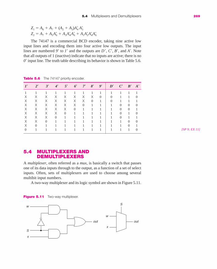
Z1 � A6 � A7 � (A2 � A3)A�4 A�5Z2 � A7 � A5A�6 � A3A�4A�6 � A1A�2A�4A�6
The 74147 is a commercial BCD encoder, taking nine active lowinput lines and encoding them into four active low outputs. The inputlines are numbered 9� to 1� and the outputs are D�, C�, B�, and A�. Notethat all outputs of 1 (inactive) indicate that no inputs are active; there is no0� input line. The truth table describing its behavior is shown in Table 5.6.
5.4 Multiplexers and Demultiplexers 269
[SP 9; EX 11]
Table 5.6 The 74147 priority encoder.
1� 2� 3� 4� 5� 6� 7� 8� 9� D� C� B� A�
1 1 1 1 1 1 1 1 1 1 1 1 1X X X X X X X X 0 0 1 1 0X X X X X X X 0 1 0 1 1 1X X X X X X 0 1 1 1 0 0 0X X X X X 0 1 1 1 1 0 0 1X X X X 0 1 1 1 1 1 0 1 0X X X 0 1 1 1 1 1 1 0 1 1X X 0 1 1 1 1 1 1 1 1 0 0X 0 1 1 1 1 1 1 1 1 1 0 10 1 1 1 1 1 1 1 1 1 1 1 0
5.4 MULTIPLEXERS AND DEMULTIPLEXERS
A multiplexer, often referred as a mux, is basically a switch that passesone of its data inputs through to the output, as a function of a set of selectinputs. Often, sets of multiplexers are used to choose among severalmultibit input numbers.
A two-way multiplexer and its logic symbol are shown in Figure 5.11.
Figure 5.11 Two-way multiplexer.
w
S
x
out
w
S
x
out
mar91647_c05a_249_285.qxd 11/14/08 12:16 PM Page 269

The output, out, equals w if S � 0, and equals x if S � 1.A four-way multiplexer can be implemented with AND and OR
gates, as shown in Figure 5.12a, or with three two-way multiplexers, asshown in Figure 5.12b. The logic symbol is shown in Figure 5.12c.
270 Chapter 5 Designing Combinational Systems
Figure 5.12 (a) A four-way multiplexer. (b) From two-way multiplexers. (c) Logic symbol.
w
Select Inputs
x
y
z
S1 S0
out
Dat
a In
puts
(a)
w
x
y
z
S1
S0 out
(b)
w
z
y
x
S0S1
out
(c)
The output equals input w if the select inputs (S1, S0) are 00, x if they are01, y if they are 10, and z if they are 11. The circuit is very similar to thatof the decoder, with one AND gate for each select input combination.Some multiplexers also have enable inputs, such that out is 0 unless theenable is active.
If the inputs consist of a set of 16-bit numbers, and the control inputschoose which of these numbers is to be passed on, then we would need16 multiplexers, one for each bit. We could build 16 of the circuits of Figure 5.12a, utilizing 64 three-input AND gates and 16 four-input ORgates. (Of course, all of the gates could be replaced by NAND gates.)
mar91647_c05a_249_285.qxd 11/14/08 12:16 PM Page 270

The alternative is to use one decoder to drive all the multiplexers. Thefirst 3 bits of such a circuit are shown in Figure 5.13.
There are still 16 four-input OR gates, but now the AND gates in themultiplexers require only two inputs. There are, of course, 4 two-inputAND gates in the decoder. The total is then 68 two-input gates for a 16-bit multiplexer. If we were to implement this with 7400 series inte-grated circuits, this implementation would require 17 packages of two-input AND gates (four to a package), whereas the previous solution wouldrequire 22 packages of three-input AND gates (three to a package).
5.4 Multiplexers and Demultiplexers 271
Figure 5.13 A multibit multiplexer.
w0
Decoder
x0
y0
z0
w1
x1
y1
z1
w2
x2
y2
z2
S1
3 2 1 0
S0
out0
out1
out2
mar91647_c05a_249_285.qxd 11/14/08 12:16 PM Page 271

Multiplexers can be used to implement logic functions. The simplestapproach is to use the select inputs to make a decoder and connect theconstants 0 and 1 to the data inputs.
272 Chapter 5 Designing Combinational Systems
A three-variable function can be directly implemented with an eight-waymultiplexer. The three variables go to the control inputs. The truth table forthe function is then connected to the data inputs.
For f (a, b, c) = �m(0, 1, 2, 5), the truth table is
a b c f
0 0 0 10 0 1 10 1 0 10 1 1 01 0 0 01 0 1 11 1 0 01 1 1 0
With a mux, it would be implemented by
EXAMPLE 5.5
1
1
1
1
0
0
0
0
f
a b c
We could also use a four-way multiplexer. To do this, we would rewrite thetruth table as follows.
f fa b c = 0 c = 1
0 0 1 1 10 1 1 0 c�1 0 0 1 c1 1 0 0 0
mar91647_c05a_249_285.qxd 11/14/08 12:16 PM Page 272
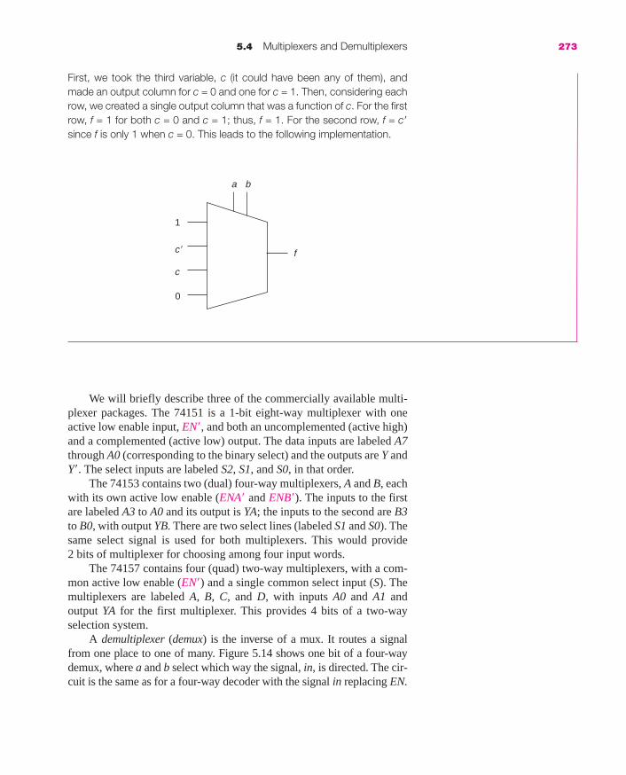
5.4 Multiplexers and Demultiplexers 273
We will briefly describe three of the commercially available multi-plexer packages. The 74151 is a 1-bit eight-way multiplexer with oneactive low enable input, EN�, and both an uncomplemented (active high)and a complemented (active low) output. The data inputs are labeled A7through A0 (corresponding to the binary select) and the outputs are Y andY�. The select inputs are labeled S2, S1, and S0, in that order.
The 74153 contains two (dual) four-way multiplexers, A and B, eachwith its own active low enable (ENA� and ENB�). The inputs to the firstare labeled A3 to A0 and its output is YA; the inputs to the second are B3to B0, with output YB. There are two select lines (labeled S1 and S0). Thesame select signal is used for both multiplexers. This would provide 2 bits of multiplexer for choosing among four input words.
The 74157 contains four (quad) two-way multiplexers, with a com-mon active low enable (EN�) and a single common select input (S). Themultiplexers are labeled A, B, C, and D, with inputs A0 and A1 andoutput YA for the first multiplexer. This provides 4 bits of a two-wayselection system.
A demultiplexer (demux) is the inverse of a mux. It routes a signalfrom one place to one of many. Figure 5.14 shows one bit of a four-waydemux, where a and b select which way the signal, in, is directed. The cir-cuit is the same as for a four-way decoder with the signal in replacing EN.
0
c
f
a b
1
c �
First, we took the third variable, c (it could have been any of them), andmade an output column for c = 0 and one for c = 1. Then, considering eachrow, we created a single output column that was a function of c. For the firstrow, f = 1 for both c = 0 and c = 1; thus, f = 1. For the second row, f = c�
since f is only 1 when c = 0. This leads to the following implementation.
mar91647_c05a_249_285.qxd 11/14/08 12:16 PM Page 273

274 Chapter 5 Designing Combinational Systems
Figure 5.14 A four-way demux.
in a b
out0
out1
out2
out3
[SP 10, 11, 12; EX 12, 13, 14; LAB]
5.5 THREE-STATE GATESUp to this point, we assumed that all logic levels were either 0 or 1.Indeed, we also encountered don’t care values, but in any real circuitimplementation, each don’t care took on either the value 0 or 1. Further-more, we never connected the output of one gate to the output of anothergate, since if the two gates were producing opposite values, there wouldbe a conflict. (In some technologies, it is possible to connect the outputof two AND gates and achieve a “wired AND” or a “wired OR,” but inothers, there is a real possibility that one or more of the gates would bedestroyed. Thus, we have not suggested this option in anything we havediscussed so far.)
Some design techniques have been used that do allow us to connectoutputs to each other. The more commonly used one today is referred toas three-state (or tristate) output gates. (We will not discuss other simi-lar implementations, such as transmission gates and open-collectorgates.)
In a three-state gate, there is an enable input, shown on the side ofthe gate. If that input is active (it could be active high or active low), thegate behaves as usual. If the control input is inactive, the output behaves as if it is not connected (as an open circuit). That output is typically represented by a Z. The truth table and the circuit representa-tion of a three-state buffer (with an active high enable) is shown in Fig-ure 5.15.
1
a
00
EN
0
01
Z
f
Z
0
111
EN
a f
Figure 5.15 A three-state buffer.
mar91647_c05a_249_285.qxd 11/14/08 12:16 PM Page 274

5.5 Three-State Gates 275
Three-state buffers with active low enables and/or outputs exist; inthe latter case, it is a three-state NOT gate. Three-state outputs also existon other more complex gates. In each case, they behave normally whenthe enable is active and produce an open circuit output when it is not.With three-state gates, we can build a multiplexer without the OR gate.For example, the circuit of Figure 5.16 is a two-way multiplexer. Theenable is the control input, determining whether f � a (EN � 0) or f � b(EN � 1). The three-state gate is often used for signals that travelbetween systems.
A bus is a set of lines over which data are transferred. Sometimes,that data may travel in either direction between devices located physi-cally at a distance. The bus itself is really just a set of multiplexers, onefor each bit in the set.
Figure 5.16 A multiplexer usingthree-state gates.
a
EN
b
f
SystemA
SystemA
SystemB
SystemB
Enable A
Enable B
Enable A
Enable B
� �
(a) Using AND/OR Gates (b) Using Three-State Gates
�
The following circuits show a bit of two implementations of the bus—oneusing AND and OR gates and the other using three-state gates.
The major difference is the two long wires per bit between the systems forthe AND-OR multiplexer compared to only one for the three-state version.The difference is even greater if what is being transferred between systemsis 32-bit words. In that case, there would be 32 multiplexers. The AND–ORsystem would require 64 wires between systems, whereas the three-stateversion would require only 32. Further, if the enable signal came from one ofthe systems (instead of being generated internally in each), that would onlyadd one wire, no matter how long the words are.
EXAMPLE 5.6
mar91647_c05a_249_285.qxd 11/14/08 12:16 PM Page 275

276 Chapter 5 Designing Combinational Systems
*A more general term is a programmable logic device (PLD). That includes all of these,as well as devices that include gate arrays and memory. The term field programmablegate array (FPGA) is also commonly used for such devices.
Figure 5.17 Structure of a gate array.
When we discuss gate arrays, both in this chapter and in Chapter 8,we will see that many systems have three-state output buffers.
5.6 GATE ARRAYS*—ROMs, PLAs, AND PALs
Gate arrays are one approach to the rapid implementation of fairlycomplex systems. They come in several varieties, but all have much incommon. The basic concept is illustrated in Figure 5.17 for a systemwith three inputs and three outputs where the dashed lines indicatepossible connections. (This is much smaller than most real gate arrays.)
mar91647_c05a_249_285.qxd 11/14/08 12:16 PM Page 276

5.6 Gate Arrays—ROMs, PLAs, and PALs 277
What these devices implement are SOP expressions. (In this case, threefunctions of three variables can be implemented. However, since thereare only six AND gates, a maximum of six different product terms can beused for the three functions.) The array only requires uncomplementedinputs; there is internal circuitry that produces the complement.
The following circuit shows the implementation of
f � a�b� � abc
g � a�b�c� � ab � bc
h � a�b� � c
using such an array, where the solid lines show the actual connections.
a b
a�b �
a�b �c �
abc
ab
bc
c
c
f g h
EXAMPLE 5.7a
mar91647_c05a_249_285.qxd 11/14/08 12:16 PM Page 277
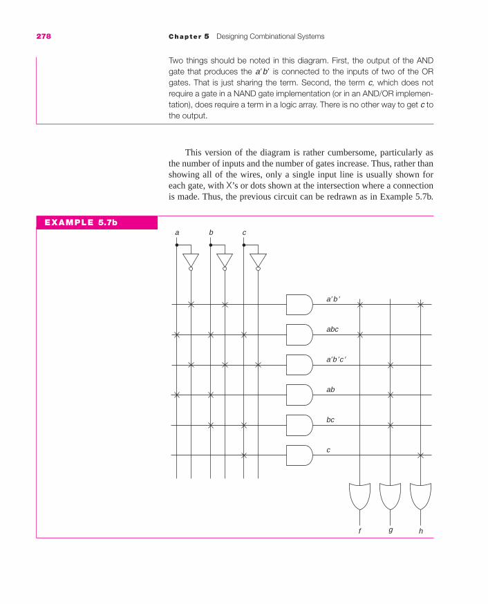
This version of the diagram is rather cumbersome, particularly asthe number of inputs and the number of gates increase. Thus, rather thanshowing all of the wires, only a single input line is usually shown foreach gate, with X’s or dots shown at the intersection where a connectionis made. Thus, the previous circuit can be redrawn as in Example 5.7b.
278 Chapter 5 Designing Combinational Systems
Two things should be noted in this diagram. First, the output of the ANDgate that produces the a�b� is connected to the inputs of two of the ORgates. That is just sharing the term. Second, the term c, which does notrequire a gate in a NAND gate implementation (or in an AND/OR implemen-tation), does require a term in a logic array. There is no other way to get c tothe output.
a b
a�b �
a�b �c �
abc
ab
bc
c
c
f g h
EXAMPLE 5.7b
mar91647_c05a_249_285.qxd 11/14/08 12:16 PM Page 278

5.6 Gate Arrays—ROMs, PLAs, and PALs 279
Sometimes, the AND and OR gates are not shown but are understood.(We will see examples of this shortly.)
There are three common types of combinational logic arrays. (We willdiscuss those with memory in Chapter 8.) The most general type (the onewe have illustrated so far) is the Programmable Logic Array (PLA). In thePLA, the user specifies all of the connections (in both the AND array andin the OR array). Thus, we can create any set of SOP expressions (andshare common terms). The second type is the Read-Only Memory (ROM).In a ROM, the AND array is fixed. It is just a decoder, consisting of 2n AND gates for an n-input ROM. The user can only specify the connec-tions to the OR gate. Thus, he produces a sum of minterms solution. Thethird type is the Programmable Array Logic (PAL), where the connectionsto the OR gates are specified; the user can determine the AND gate inputs.Each product term can be used only for one of the sums. We will discusseach of these in more detail in the sections that follow.
In each case, the base array is manufactured first, with the connec-tions added later. One option is to have them added by the manufactureron the user’s specifications. There are also field programmable versions,where the user can enter the connections using a special programmingdevice. The concept behind field programmable devices is to include afuse in each connection line. If the user does not want the connection, heblows the fuse. (A blown fuse produces a 1 input to the AND gates and a0 input to the OR gates. That fuse may be electronic, in which case itmay be reset.) This sounds more complicated and time consuming thanit is; the programming device does all of this automatically from inputsdescribing the desired array. This idea is carried one step further in thecase of ROMs; there are Erasable Programmable Read-Only Memories(EPROMs). (This does sound like an oxymoron, to have a writable read-only device, but they do exist.) One type of fuse can be reset by exposingthe device to ultraviolet light for several minutes; another type can bereset electronically.
In addition to the logic shown above, many field programmabledevices make the output available in either active high or active lowform. (By active low, we really mean the complement of the output, thatis, f � instead of f.) This just requires an Exclusive-OR gate on the outputwith the ability to program one of the inputs to 0 for f and to 1 for f �. Theoutput logic for such a case is shown in Figure 5.18.
f
0 or 1
f � 0 � ff � 1 � f �
Figure 5.18 A programmableoutput circuit.
mar91647_c05a_249_285.qxd 11/14/08 12:16 PM Page 279

Note that if the three-state gate is enabled, the connection from theOR array to the output and back as an input to the AND array is estab-lished. If the three-state gate is not enabled, the logic associated with thatOR is disconnected, and this Out/In can be used as just another input tothe AND array.
5.6.1 Designing with Read-Only Memories
To design a system using a ROM, you need only to have a list ofminterms for each function. A ROM has one AND gate for eachminterm; you connect the appropriate minterm gates to each output. Thisis really the same type of circuitry as the decoder implementation of asum of product expression presented in Example 5.3.
280 Chapter 5 Designing Combinational Systems
EN
Out/In
AND Array
Figure 5.19 Three-state output.
Some programmable devices have a three-state buffer at the output,which may be enabled either by an enable input line or one of the logicAND gates. This allows the output to be easily connected to a bus.
Sometimes, the output is fed back as another input to the AND array.This allows for more than two-level logic (most commonly in PALs, aswe will discuss later). It also allows that output to be used as an inputinstead of an output, if a three-state output gate is added, as shown inFigure 5.19.
W ( A, B, C, D) � m(3, 7, 8, 9, 11, 15)
X ( A, B, C, D) � m(3, 4, 5, 7, 10, 14, 15)
Y ( A, B, C, D) � m(1, 5, 7, 11, 15)
The rows of the ROM are numbered (in order) from 0 to 15 for the four-inputROM shown here. An X or a dot is then placed at the appropriate intersec-tion. In the following circuit, the connections shown as X’s are built into theROM; the user supplied the ones shown as dots to implement the functionsabove.
EXAMPLE 5.8
mar91647_c05a_249_285.qxd 11/14/08 12:16 PM Page 280

5.6 Gate Arrays—ROMs, PLAs, and PALs 281
In spite of the terminology, that is, referring to this device as amemory, it is really a combinational logic device, as used in a circuit.The outputs are just a function of the present inputs. In Chapter 8, wewill see programmable devices that do have memory in them. Typicalcommercial programmable ROMs have 8 to 12 inputs and 4 to 8 outputs.
5.6.2 Designing with ProgrammableLogic Arrays
To design a system using a PLA, you need only find SOP expressions forthe functions to be implemented. The only limitation is the number ofAND gates (product terms) that are available. Any SOP expression foreach of the functions will do, from just a sum of minterms to one thatminimizes each function individually to one that maximizes sharing(uses the techniques of Section 3.6).
BA C D
W X Y
0
1
2
3
4
5
6
7
8
9
10
11
12
13
14
15
Consider the same example we used to illustrate the ROM design:
W ( A, B, C, D) � m(3, 7, 8, 9, 11, 15)
X ( A, B, C, D) � m(3, 4, 5, 7, 10, 14, 15)
Y ( A, B, C, D) � m(1, 5, 7, 11, 15)
EXAMPLE 5.9
mar91647_c05a_249_285.qxd 11/14/08 12:16 PM Page 281

282 Chapter 5 Designing Combinational Systems
The first set of maps shows the solution considering these as individualfunctions. X and Y have two solutions.
00 01 11 10
00
01
11
10
A B
W X Y
C D
1 1 11
1
1
00 01 11 10
00
01
11
10
A BC D
11 1
1 1
1
1
00 01 11 10
00
01
11
10
A BC D
1 1 1
11
W � AB�C� � CD
Y � A�BC� � A�CD � ACD� � {BCD or ABC}
Z � A�C�D � ACD � { A�BD or BCD}
If we choose BCD for both Y and Z, this solution requires eight terms.Otherwise, it requires nine terms.
We can use fewer terms, by treating this as a multiple-output problem,as shown in the following maps:
00 01 11 10
00
01
11
10
A B
W X Y
C D
1 1 11
1
1
00 01 11 10
00
01
11
10
A BC D
11 1
1 1
1
1
00 01 11 10
00
01
11
10
A BC D
1 1 1
11
W � AB�C� � A�CD � ACD
X � A�BC� � ACD� � A�CD � BCD
Y � A�C�D � ACD � BCD
This solution only uses seven terms instead of eight or nine.The following PLA shows both solutions. In the first set of output
columns, we show the first solution. The first eight terms are used or the
mar91647_c05a_249_285.qxd 11/14/08 12:16 PM Page 282
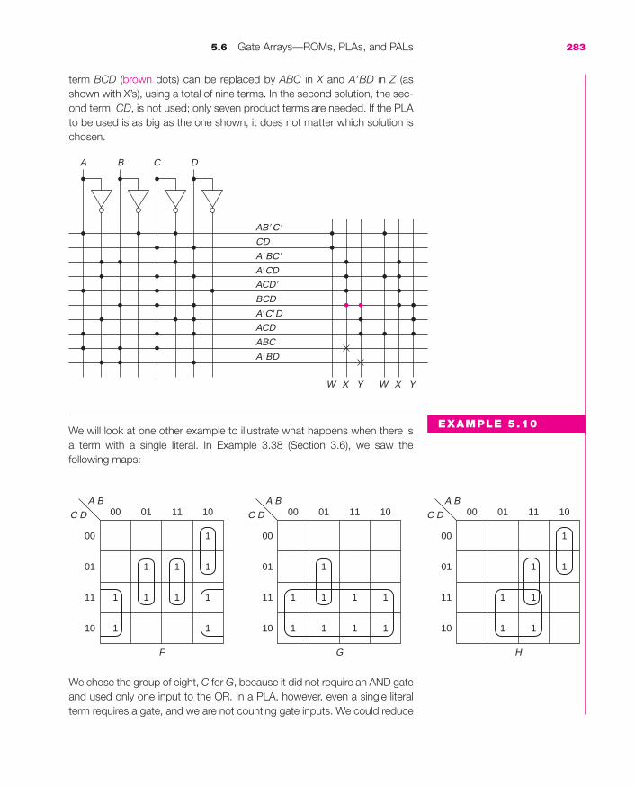
5.6 Gate Arrays—ROMs, PLAs, and PALs 283
term BCD (brown dots) can be replaced by ABC in X and A�BD in Z (asshown with X’s), using a total of nine terms. In the second solution, the sec-ond term, CD, is not used; only seven product terms are needed. If the PLAto be used is as big as the one shown, it does not matter which solution ischosen.
BA C D
W X Y W X Y
AB�C�
CD
A�BC�
A�CDACD�
BCD
A�C�DACD
ABC
A�BD
We will look at one other example to illustrate what happens when there isa term with a single literal. In Example 3.38 (Section 3.6), we saw thefollowing maps:
00 01 11 10
00
01
11
10
A B
F G H
C D
1 1 1
1
1
1
1
111
00 01 11 10
00
01
11
10
A BC D
1
1
1
1
1
1 1
1
1
00 01 11 10
00
01
11
10
A BC D
1
1
1
1
1
1
1
We chose the group of eight, C for G, because it did not require an AND gateand used only one input to the OR. In a PLA, however, even a single literalterm requires a gate, and we are not counting gate inputs. We could reduce
EXAMPLE 5.10
mar91647_c05a_249_285.qxd 11/14/08 12:16 PM Page 283

A typical commercially available PLA (PLS100) has 16 inputs,48 product terms, and 8 outputs. Each output is programmable to be activehigh or low and has a three-state buffer, controlled by a common active lowenable input. Note that this is less than one thousandth the number of prod-uct terms that would be required for a ROM with 16 inputs.
5.6.3 Designing with ProgrammableArray Logic
In a PAL, each output comes from an OR that has its own group of ANDgates connected to it. The layout of a small PAL is shown in Figure 5.20.
For this PAL, there are six inputs and four outputs, with each OR gatehaving four input terms. When using a PAL, the output of each AND gategoes to only one OR. Thus, there is no sharing of terms, and we wouldsolve each function individually. However, most PALs provide for the pos-sible feedback of some or all of the outputs to an input. Sometimes this isinternal, that is, the output of some of the OR gates is available as anotherinput to all of the AND gates. In other cases, an external connection ismade (as implied in Example 5.12). This allows for more terms (more than
284 Chapter 5 Designing Combinational Systems
the number of terms needed by using BC � B�C for G, since B�C wasrequired for F and BC was required for H. Thus, either set of output columnsin the following PLA diagram would be a solution. Note that the term C isonly used in the first implementation; the second requires one less term.
BA C D
F G H F G H
B�C
AB�C�
A�BD
ABDBC
C
mar91647_c05a_249_285.qxd 11/14/08 12:16 PM Page 284
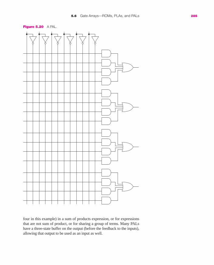
5.6 Gate Arrays—ROMs, PLAs, and PALs 285
four in this example) in a sum of products expression, or for expressionsthat are not sum of product, or for sharing a group of terms. Many PALshave a three-state buffer on the output (before the feedback to the inputs),allowing that output to be used as an input as well.
Figure 5.20 A PAL.
mar91647_c05a_249_285.qxd 11/14/08 12:16 PM Page 285

286 Chapter 5 Designing Combinational Systems
We will first return to the example we used for ROMs and PLAs, namely,
W � AB�C� � CD
X � A�BC� � A�CD � ACD� � {BCD or ABC}
Y � A�C�D � ACD� � {A�BD or BCD}
There is no reason to consider sharing. Choosing the first of each of theoptional terms, the implementation is
A B C D
W
X
Y
EXAMPLE 5.11
mar91647_c05b_286_318.qxd 11/14/08 12:17 PM Page 286

5.6 Gate Arrays—ROMs, PLAs, and PALs 287
h
00 01 11 10
00
01
11
10
a b
c d
11 1
111
1
00 01 11 10
00
01
11
10
a b
f g
c d
11
11
111
00 01 11 10
00
01
11
10
a b
c d
1
1 1
111
1
Note that the three brown terms are essential prime implicants of each func-tion; the other two are not. This results in the following equations:
f � a�b�c� � a�c�d � b�c�d � abd� � bcd�
g � a�b�c� � a�c�d � b�c�d � abc � acd�
h � a�b�c� � a�c�d � b�c�d � a�cd� � b�cd�
(This solution was obtained by considering each function individually. If wetreated this as a multiple-output problem, we would use the term ab�cd� inboth g and h, rather than acd� in g and b�cd� in h. That would reduce thenumber of different terms in the algebraic solution, but it would not changethe number of gates used in the PAL.) The PAL implementation is shown inthe following circuit. The first three terms are implemented in the first ORgate, the output of which, t, is fed back to the input of one of the ANDgates in each of the other three circuits. Note that the fourth AND gate ofthe t circuit has both a and a� connected at its input. Obviously, the outputof that AND gate is 0. Some implementations require the user to connectunused AND gates in that way. (We did not do that for the other unusedAND gates.)
As an example of a system where feedback is useful, consider the functionsshown in the following maps:
EXAMPLE 5.12
mar91647_c05b_286_318.qxd 11/14/08 12:17 PM Page 287

288 Chapter 5 Designing Combinational Systems
a b c d t
t
f
g
h
[SP 13, 14; EX 15, 16, 17]
mar91647_c05b_286_318.qxd 11/14/08 12:17 PM Page 288

5.7 Testing and Simulation of Combinational Systems 289
*For a detailed discussion of Verilog or VHDL, see Brown and Vranesic, Fundamentalsof Digital Logic with Verilog Design, 2nd ed. McGraw-Hill, 2008 or Brown and Vranesic,Fundamentals of Digital Logic with VHDL Design, 3rd ed. McGraw-Hill, 2009.
5.7 TESTING AND SIMULATION OFCOMBINATIONAL SYSTEMS
After designing a system, it is necessary to test it to make sure that it doeswhat it was intended to do. For a small system, this means applying all pos-sible input combinations and comparing the output with what was expected.As systems get a little larger, that process becomes very time-consuming.For example, if we are testing the behavior of a 4-bit adder (with carryinput), there are 29 input combinations to test. We can be sure that it worksby trying many fewer input sets, as long as we are careful to make sure thatall parts of the circuit are tested (each sum circuit and each carry circuit).
When building a large system, it is often necessary to break it intoseveral smaller systems and design and test each subsystem separately.If you are building a large number of a particular system, you wouldnormally design an integrated circuit. Before committing to that design,you must test the design, either by building a circuit using small-scalecomponents or simulating it.
5.7.1 An Introduction to Verilog
Most design of significant digital systems is done with computer-aidedtools. They allow the user to specify either the behavior of the system orthe structure of the system (or a mixture of the two) using a notation sim-ilar to a programming language. The two most widely used systems areVerilog and VHDL. They have many similarities, but differ in detail. Inthis section, we will show examples of Verilog code, both structural andbehavioral, but a discussion adequate to allow the user to design usingany HDL is beyond the scope of this book.*
We will first illustrate a structural Verilog description, using the fulladder first discussed in Example 2.34 and shown here as Figure 5.21.
Figure 5.21 A full adder.
a
bc
s
c_out
x 1
n 1
n 2
n 3
x 2
w 3
w 2
w 1
mar91647_c05b_286_318.qxd 11/14/08 12:17 PM Page 289

The corresponding Verilog code (description) is shown in Figure 5.22.
290 Chapter 5 Designing Combinational Systems
Figure 5.22 Verilog structural description of a full adder.
module full_adder (c_out, s, a, b, c);input a, b, c;wire a, b, c;output c_out, s;wire c_out, s;wire w1, w2, w3;xor x1 (w1, a, b);xor x2 (s, w1, c);
nand n1 (w2, a, b);nand n2 (w3, w1, c);nand n3 (c_out, w3, w2);
endmodule
Figure 5.23 A 4-bit adder.
module adder_4_bit (c, sum, a, b);input a, b;output c, sum;wire [3:0] a, b, sum;wire c0, c1, c2, c;full_adder f1 (c0, sum[0], a[0], b[0], 'b0);full_adder f2 (c1, sum[1], a[1], b[1], c0);full_adder f3 (c2, sum[2], a[2], b[2], c1);full_adder f4 (c, sum[3], a[3], b[3], c2);
endmodule
The first line includes the key word module followed by the name of themodule and the parameters, that is, the outputs and the inputs. Names mayinclude characters other than spaces; Verilog is case-sensitive, that is x1means something different from X1. (The symbol _ is used to connect mul-tiple word names.) Each module ends with the statement endmodule.Statements within Verilog are ended with a semicolon (;), other thanendmodule. A list of inputs and outputs must be included, and eachgate output must be declared a wire. Structural Verilog includes moststandard gate types, such as and, or, not, nand, nor, xor. Theyare indicated by listing the key word (such as xor), a unique name foreach copy of that device, their output wire name, and their inputs, asshown in Figure 5.22. The connections for the circuit are made exactly asin Figure 5.21. The order in which the logic statements are written doesnot matter. (That is not true in behavioral Verilog.)
A 4-bit adder can be built using the full adder as a building block, asshown in Figure 5.23. (We will use a full adder for the least significantbit, although a half adder would do.)
mar91647_c05b_286_318.qxd 11/14/08 12:17 PM Page 290

5.7 Testing and Simulation of Combinational Systems 291
Some additional notation appears in this example. Multibit wires arelabeled with brackets. The wire [3:0] a, b, sum declaration statesthat each of the inputs and the sum output are 4 bits (with the highest num-ber on the left. When a module is used, such as full_adder, the order ofthe parameters is what matters, not the name. Thus, the first copy of the fulladder adds the least significant bits, a[0] and b[0], with a 0 in the carryposition (denoted as 'b0, where the 'b indicates that the number follow-ing it is binary).
Verilog also provides for the description of the behavior of a system,without specifying the details of the structure. This is often the first stepin the design of a complex system, made up of a number of modules. Thebehavioral description of each module can be completed and tested. Thatis often much more straightforward. Once that works, the individualmodules can be designed and described structurally. The structuraldescription can then replace the behavioral one, one module at a time.Behavioral Verilog uses notation very similar to the C programminglanguage. The normal mathematics operators (such as �, �, *, and / )are available, as are the bitwise logical operators (not: ~, and: &, or: |,and exclusive or: ^). Two behavioral Verilog descriptions of the fulladder are shown in Figure 5.24.
Figure 5.24 Behavioral Verilog for the full adder.
module full_adder (c_out, s, a, b, c);input a, b, c;wire a, b, c;output c_out, s;reg c_out, s;always
begins = a ^ b ^ c;c_out = (a & b) | (a & c_in) | (b & c_in);
endendmodule
(a) With logic equations.
module full_adder (c_out, s, a, b, c);input a, b, c;wire a, b, c;output c_out, s;reg c_out, s;always
{c_out, s} � a � b � c;endmodule
(b) With algebraic equations.
mar91647_c05b_286_318.qxd 11/14/08 12:17 PM Page 291

Note that values set in behavioral models are referred to as reg, ratherthan wire.
5.8 LARGER EXAMPLESIn this section, we will look at the design of three systems that are some-what larger than any we have considered so far.
5.8.1 A One-Digit Decimal Adder
We want to design an adder to add two decimal digits (plus a carry-in),where the digits are stored in 8421 code. This system would have nineinputs (two coded digits plus the carry-in) and five outputs (the one digitand the carry-out). Rather than trying to solve a nine-input problem, wecan break it up into smaller parts, using the 4-bit binary adder that wealready designed (or obtained on a single chip). We will assume thatnone of the unused inputs ever occur.
Decimal addition can be performed by first doing binary addition.Then, if the sum is greater than 9, a carry is generated and 6 is added tothis digit. (That is to make up for the six combinations that are not used).For example,
292 Chapter 5 Designing Combinational Systems
We add the two numbers using a binary adder and detect whether thesum is greater than 10. If it is, we must add six (0110) to the result. Ablock diagram of the decimal adder, using two binary adders, is shown inFigure 5.25.
The carry detect circuit takes the output of the first adder (includingthe carry) and produces a 1 output if that number is greater than 9. Thatis the carry output from the decimal adder, as well as the correction indi-cator. When there is a carry-out, 6 is added to the answer from the firstadder; otherwise, 0 is added. A map for the carry detect circuit is shownas Map 5.2.
0 1 1
0011 3 0111 7 1000 8
0101 5 0101 5 1001 9
0 1000 8 0 1100 – – 1 0010 1 2
sum � 9 0110 6 0110 6
no correction 1 0010 1 2 1 1000 1 8
mar91647_c05b_286_318.qxd 11/14/08 12:17 PM Page 292
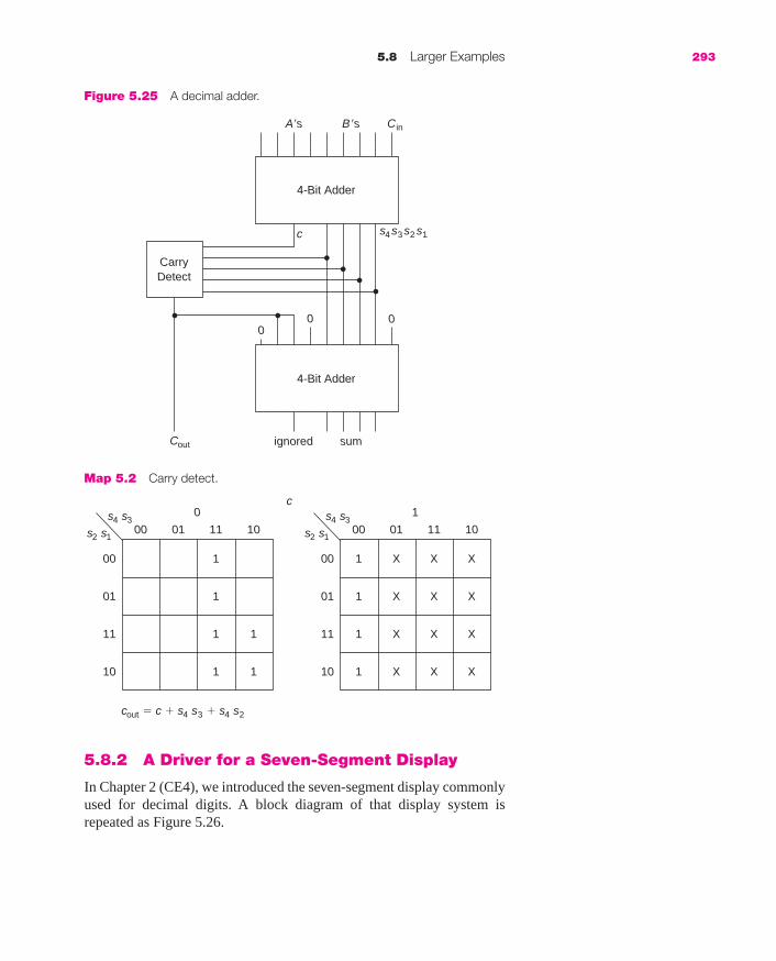
5.8 Larger Examples 293
Map 5.2 Carry detect.
cout � c � s4 s3 � s4 s2
00 01 11 10
00
01
11
10
s4 s3
1
0
11
1
11
s2 s100 01 11 10
00
01
11
10
s4 s31
X
X
X
X
X
X
X
X
X
X
X
X
1
1
1
1
c
s2 s1
Figure 5.25 A decimal adder.
CarryDetect
4-Bit Adder
4-Bit Adder
A�s B�s
s4s3s2s1
Cin
Cout sumignored
c
000
5.8.2 A Driver for a Seven-Segment Display
In Chapter 2 (CE4), we introduced the seven-segment display commonlyused for decimal digits. A block diagram of that display system isrepeated as Figure 5.26.
mar91647_c05b_286_318.qxd 11/14/08 12:17 PM Page 293

where the solid lines represent segments to be lit and the dashed onessegments that are not lit. For digits 6, 7, and 9, two alternative rep-resentations are shown (that is, one segment of each may or may not be lit).
This display driver is a problem with four inputs, W, X, Y, and Z andseven outputs, a, b, c, d, e, f, and g. If, indeed, the system is to display onlya decimal digit, and the inputs are limited to only proper codes for thosedigits, then only 10 of the possible 16 input combinations can occur. Theothers can be treated as don’t cares. In Section 2.1.2, we chose the 8421code (straight binary) to represent the decimal digits and showed the truthtable under the assumption that a 1 input to the display would cause thatsegment to be lit. Although this seems like a natural assumption, displaysare available that require a 0 on a segment input to light that segment.
There are several approaches to this design. There are BCD-to-seven-segment converters available, such as the 7449, that could be used for thisproblem. (There are also chips that produce an active low output.)
We could solve each of these as individual functions (as in Sec-tion 3.3), or we could treat them as multiple-output problems, as in Section 3.6. We could also use a ROM, a PLA, or a PAL to complete thedesign. We will design the ROM and PLA solution for this problem.
Solving each as an individual function is very straightforward.There are several prime implicants that can be shared. The minimum is obtained by choosing one of the multiple solutions for g that takesadvantage of sharing. A minimum solution, shown in Map 5.3, is
a � W � Y � XZ � X�Z�
b � X� � YZ � Y�Z�
c � X � Y� � Z
d � X�Z� � YZ� � X�Y � XY�Z
e � X�Z� � YZ�
f � W � X � Y�Z�
g � W � X�Y � XY� � {XZ� or YZ�}
294 Chapter 5 Designing Combinational Systems
Figure 5.26 A seven-segment display and driver.
a
DisplayDriver
W
X
Y
Z
a
gf b
e c
d
dcb
efg
mar91647_c05b_286_318.qxd 11/14/08 12:17 PM Page 294

5.8 Larger Examples 295
Map 5.3 Seven-segment display driver.
00 01 11 10
00
01
11
10
W X
Y Z
a
c
e
g
X X X
1X
X
X X
1
1
1
11
1
00 01 11 10
00
01
11
10
W X
Y Z
1
1 1
1
1
1
1
X
X
X
X
X
X
X
X
X
X
X
X
X
X
X
X
X
X
X
X
X
X
X
X
1
1
00 01 11 10
00
01
11
10
W X
Y Z
11
1 1
00 01 11 10
00
01
11
10
W X
Y Z
11
1
1
11
1
b
d
f
00 01 11 10
00
01
11
10
W X
Y Z
11
1
1
1 1 X
X
1X
1X
1
1
00 01 11 10
00
01
11
10
W X
Y Z
XX
X
XX
XX
1
1
1
1
1
1
00 01 11 10
00
01
11
10
W X
Y Z
11
1
1 1 1
X
mar91647_c05b_286_318.qxd 11/14/08 12:17 PM Page 295

where the shared terms are shown in brown, tan, and gray. There areeight unique terms requiring gates (since single literal terms do notrequire a gate). Thus, this would require a total of 15 gates, assuming allinputs are available both uncomplemented and complemented. (Other-wise, four additional NOT gates would be required.) If these were imple-mented with 7400 series NAND gates, then we would use
296 Chapter 5 Designing Combinational Systems
Type Number Number of modules Chip number
2-in 8 2 74003-in 4 1 74104-in 3 2 7420
where only one 7410 is required since the extra four-input gate would beused as the fourth three-input gate. Treating this as a multiple-output prob-lem, we could save one gate by using XY�Z in function a in place of XZ.
A more interesting problem (in the sense that there is more of anadvantage to treating the problem as a multiple-output one) results if wedemand that all segments be unlit if the code is not one of those used fora decimal digit. The maps for this, with the minimum solutions circled,are shown in Map 5.4. All of the don’t cares for minterms 10 to 15 havebecome 0’s. (The don’t cares for the alternative representations of 6, 7,and 9 remain.) The shared prime implicants are shown circled in brown,tan, and gray. (There are multiple solutions to several of the functions;the one that provides the maximum sharing is shown.)
One way to display the answer is shown in Table 5.7, with a row foreach product term and a column for each function. An X is placed in thecolumn if that product term is used in the function.
Table 5.7 Seven-segment display driver (prime implicants only).
a b c d e f g
X�Y�Z� X X XWX�Y� X X XW�Y XW�XZ XW�Y�Z� X XW�X� XW�YZ XX�Y� X XW�X X XW�Z XW�YZ� X X XW�X�Y X XW�XY�Z XW�XY� X
mar91647_c05b_286_318.qxd 11/14/08 12:17 PM Page 296

5.8 Larger Examples 297
Map 5.4 Seven-segment display driver (individual).
00 01 11 10
00
01
11
10
W X
Y Z
a
c
e
g
X
11
1
1
11
1
00 01 11 10
00
01
11
10
W X
Y Z
1
1 1
1
1
1
1
1
1
00 01 11 10
00
01
11
10
W X
Y Z
11
1 1
00 01 11 10
00
01
11
10
W X
Y Z
11
1
1
11
1
b
d
f
00 01 11 10
00
01
11
10
W X
Y Z
11
1
1
1 1
1
1
00 01 11 10
00
01
11
10
W X
Y Z
X1
1
1
1
1
1
00 01 11 10
00
01
11
10
W X
Y Z
11
1
1 1 1
X
mar91647_c05b_286_318.qxd 11/14/08 12:17 PM Page 297

The algebraic expressions can be obtained by just ORing the termsincluded in each function. We can count the number of gates (one foreach term, that is, each row and one for each output column). The num-ber of gate inputs is also easy to compute, since we just add the numberof literals in each term and the number of X’s in each function (corre-sponding to OR gate inputs). For this example, the total is 21 gates and62 gate inputs.
We next attempt to solve this by sharing terms wherever possible,even if the term is not a prime implicant. The first obvious spot is in a,where the prime implicant W�XZ can be replaced by the term W�XY�Z, aterm we already need for d. Map 5.5 shows a minimum solution, whereterms that are shared are shown circled in brown, tan, and gray. Thisresults in the solution of Table 5.8.
298 Chapter 5 Designing Combinational Systems
This solution requires only 10 terms and thus 17 gates, a savings of4 gates, and 54 inputs, a savings of 8 gate inputs. The correspondingequations are thus
a � X�Y�Z� � WX�Y� � W�XY�Z � W�YZ � W�X�Y
b � W�YZ � W�X�Y � W�Y�Z� � X�Y�
c � W�YZ � X�Y� � W�X
d � X�Y�Z� � W�XY�Z � W�X�Y � W�YZ�
e � X�Y�Z� � W�YZ�
f � WX�Y� � W�Y�Z� � W�X
g � WX�Y� � W�X�Y � W�YZ� � W�XY�
If we are to implement each of these with 7400 series NAND gates,the system would require
Table 5.8 Seven-segment display driver (maximum sharing).
a b c d e f g
X�Y�Z� X X XWX�Y� X X XW�XY�Z X XW�YZ X X XW�X�Y X X X XW�Y�Z� X XX�Y� X XW�X X XW�YZ� X X XW�XY� X
mar91647_c05b_286_318.qxd 11/14/08 12:17 PM Page 298

5.8 Larger Examples 299
Map 5.5 Seven-segment display driver (maximum sharing).
b
d
f
00 01 11 10
00
01
11
10
W X
Y Z
11
1
1
1 1
1
1
00 01 11 10
00
01
11
10
W X
Y Z
X1
1
1
1
1
1
00 01 11 10
00
01
11
10
W X
Y Z
11
1
1 1 1
X
00 01 11 10
00
01
11
10
W X
Y Z
a
c
e
g
X
11
1
1
11
1
00 01 11 10
00
01
11
10
W X
Y Z
1
1 1
1
1
1
1
1
1
00 01 11 10
00
01
11
10
W X
Y Z
11
1 1
00 01 11 10
00
01
11
10
W X
Y Z
11
1
1
11
1
mar91647_c05b_286_318.qxd 11/14/08 12:17 PM Page 299

Thus, we save four gates and one module by treating this as a multiple-output problem.
Notice that these two solutions are not equal. The first treats thedon’t care in d as 0 and the don’t cares in a and f as 1’s; the second treatsthe don’t cares in a and d as 0’s and only the one in f as a 1.
We could also implement this problem using the ROM shown inFigure 5.27. Note that we did not include any of the don’t cares; wecould have made any or all of them 1’s. Notice that this solution is notequal to either of the other ones, since each of them treat at least one ofthe don’t cares as 1.
300 Chapter 5 Designing Combinational Systems
Individually Multiple output
Number NumberType Chip number Number of modules Number of modules
2-in 7400 6 2 3 13-in 7410 10 3 9 34-in 7420 5 3 4 28-in 7430 0 1 1
Total 21 8 17 7
Figure 5.27 ROM implementation of seven-segment display driver.
XW Y Z
a b c d e f g
0
1
2
3
4
56
7
8
9
10
11
12
13
14
15
mar91647_c05b_286_318.qxd 11/14/08 12:17 PM Page 300
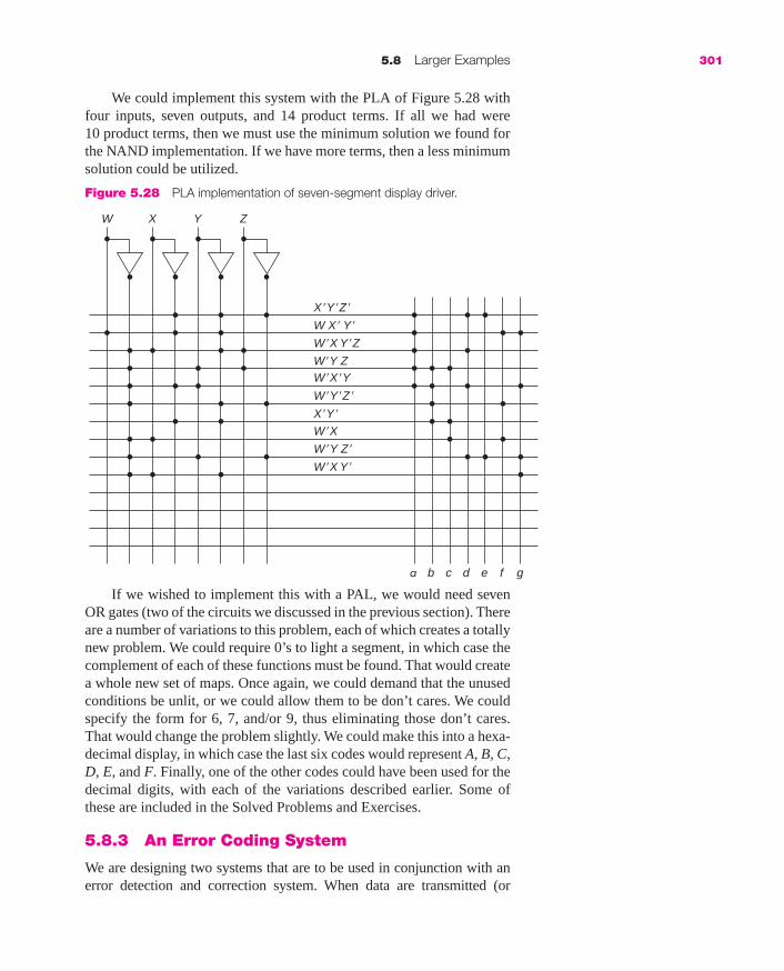
5.8 Larger Examples 301
We could implement this system with the PLA of Figure 5.28 withfour inputs, seven outputs, and 14 product terms. If all we had were 10 product terms, then we must use the minimum solution we found forthe NAND implementation. If we have more terms, then a less minimumsolution could be utilized.
If we wished to implement this with a PAL, we would need sevenOR gates (two of the circuits we discussed in the previous section). Thereare a number of variations to this problem, each of which creates a totallynew problem. We could require 0’s to light a segment, in which case thecomplement of each of these functions must be found. That would createa whole new set of maps. Once again, we could demand that the unusedconditions be unlit, or we could allow them to be don’t cares. We couldspecify the form for 6, 7, and/or 9, thus eliminating those don’t cares.That would change the problem slightly. We could make this into a hexa-decimal display, in which case the last six codes would represent A, B, C,D, E, and F. Finally, one of the other codes could have been used for thedecimal digits, with each of the variations described earlier. Some ofthese are included in the Solved Problems and Exercises.
5.8.3 An Error Coding System
We are designing two systems that are to be used in conjunction with anerror detection and correction system. When data are transmitted (or
Figure 5.28 PLA implementation of seven-segment display driver.
XW Y Z
a b c d e f g
X�Y�Z�
W X� Y�
W�X Y�Z
W�Y ZW�X�Y
W�Y�Z �
X�Y�
W�X
W�Y Z�
W�X Y�
mar91647_c05b_286_318.qxd 11/14/08 12:17 PM Page 301

302 Chapter 5 Designing Combinational Systems
stored), errors occur. Richard Hamming developed a technique for codingdata (by adding extra digits) so that a single error (that is, an error in 1 bit)can be corrected. (This can be extended to double error detection and evenmultiple error correction.) To detect an error in a set of bits, a check bit iscreated so that the total number of 1’s in the word, including the check bit,is even.* That bit is referred to as a parity bit. If one error is made, either a 1will become a 0, or a 0 will become a 1, making the total number of 1’s odd.
The parity bit can be computed by using the Exclusive-OR functionon the bits to be checked. On the receiving end, the checked bits andthe parity bit are Exclusive-ORed; if the result is 0, then the answer isassumed to be correct.† For error correction, multiple parity bits arerequired, each checking a different set of information bits. Data arecoded in such a way that a single error from any transmitted word willnot produce another transmitted word or a word that has a single errorfrom another transmitted word. (The Hamming distance between wordsis the number of digits in which they differ. For single error correction,transmitted words must be at distance 3.) For a single data bit, two checkbits are required. The two transmitted words would be 000 for data 0 and111 for data 1. A single error from 000 would produce a word with one1; thus, all words with zero or one 1 would be decoded as 0 and all wordswith two or three 1’s would be decoded as 1.
Hamming showed that for three check bits, we could have up to fourdata bits, and that for four check bits, we can have up to 11 data bits. Asan example, we will consider three data bits and three check bits, whichprovide for the correction of all single errors and the detection of somedouble errors (since some of the possible received words may not corre-spond to a transmitted word or a single error from one of those words). Ablock diagram is shown in Figure 5.29.
*The parity bit could be chosen so as to make the total number of 1’s odd, instead.†This method is not foolproof. If two errors are made, there will once again be an evennumber of 1’s, and it will look like the received word is correct. This approach is usedwhen the likelihood of multiple errors is very small.
xyz
uvw
abc
ed
fCoder
Errordetector/corrector
Transmissionmedia
p
q
r
g
Figure 5.29 Error detection and correction system.
The first check bit, u, checks x and y; v checks x and z; and w checksy and z. Thus, the coder is just
u � x � y v � x � z w � y � z
The list of transmitted words is shown in Table 5.9.
Table 5.9 Transmitted words.
Data Check
x y z u v w
0 0 0 0 0 00 0 1 0 1 10 1 0 1 0 10 1 1 1 1 01 0 0 1 1 01 0 1 1 0 11 1 0 0 1 11 1 1 0 0 0
mar91647_c05b_286_318.qxd 11/14/08 12:17 PM Page 302

For each transmitted word, there are six single errors that will bedecoded to that word (plus the correct word). For example, single errorsfrom the first word are 100000, 010000, 001000, 000100, 000010, and000001. Each of these, plus 000000, should be decoded as 000. Map 5.6shows the maps for p, q, and r—the corrected word—and for g, which is1 if a multiple error is detected (in which case, p, q, and r are not
5.8 Larger Examples 303
Map 5.6 Error detector/corrector.ab
00 01 11 10
00
01
11
10
c de f
0
0
00
0
0
0
0
X
1
1
X
0
0
0
0
0
0
00 01 11 10
00
01
11
10
c de f
0
0
01
1
X
0
0
0
0
0
0
0
0
X
1
0
0
00 01 11 10
00
01
11
10
c de f
1
1
11
1
1
0
X
1
1
1
1
X
0
1
1
1
1
00 01 11 10
00
01
11
10
c de f
X
0
10
1
1
1
1
1
1
1
1
1
1
1
1
0
X
ab
00 01 11 10
00
01
11
10
c de f
0
0
00
0
0
1
0
X
0
0
X
0
1
0
0
0
0
00 01 11 10
00
01
11
10
c de f
1
0
01
1
X
1
1
1
1
1
1
1
1
X
1
0
1
00 01 11 10
00
01
11
10
c de f
1
1
11
1
1
1
X
1
0
0
1
X
1
1
1
1
1
00 01 11 10
00
01
11
10
c de f
X
0
10
1
0
0
0
0
0
0
0
0
0
0
1
0
X
ab
00 01 11 10
00
01
11
10
c de f
0
0
00
1
0
0
0
X
0
1
X
1
1
1
0
1
1
00 01 11 10
00
01
11
10
c de f
0
0
01
0
X
0
0
0
1
0
1
1
1
X
1
1
1
00 01 11 10
00
01
11
10
c de f
0
1
11
0
0
0
X
0
0
1
1
X
1
1
1
0
1
00 01 11 10
00
01
11
10
c de f
X
0
10
0
0
1
0
0
0
1
1
1
0
1
1
1
X
ab
00 01 11 10
00
01
11
10
c de f
00
1
1
00 01 11 10
00
01
11
10
c de f
01
1
1
00 01 11 10
00
01
11
10
c de f
11
1
1
00 01 11 10
00
01
11
10
c de f
1
10
1
p
q
r
g
mar91647_c05b_286_318.qxd 11/14/08 12:17 PM Page 303

reliable). The shaded squares correspond to the words with no errors.The outputs that produce uvw � 000 are shown in brown. Squares thatdo not correspond to correct words or single errors are shown as don’tcares on the first three maps, and as 1’s on the map for g (which indicatesmultiple errors). Sum of products expressions for these functions arevery complex, requiring 30 product terms. If implemented with NANDgates, 22 integrated circuit packages would be needed.
However, the code has been set up in such a way that the correct out-puts can be determined more easily. Computing the Exclusive-OR ofeach check bit with the bits that formed it, we get
t1 � a � b � d
t2 � a � c � e
t3 � b � c � f
That test word indicates which bit is in error (if a single error was made),as described in Table 5.10.
304 Chapter 5 Designing Combinational Systems
Table 5.10 Bit error.
t1 t2 t3 Error
0 0 0 none0 0 1 f0 1 0 e0 1 1 c1 0 0 d1 0 1 b1 1 0 a1 1 1 multiple
The decoder circuit can then be built with three 7486 (quad Exclusive-OR)packages and one three-input/eight-output decoder (such as the one usedin Example 5.3), as shown in Figure 5.30.
Figure 5.30 Error decoder.
0
1
4
5
6
7
2
3
Decoder
a
a
b
c
c
e
b
d
f
t1
t2
t3
p
q
r
c
b
a
g
[SP 15, 16, 17, 18; EX 18, 19, 20, 21, 22, 23, 24, 25; LAB]
mar91647_c05b_286_318.qxd 11/14/08 12:17 PM Page 304

5.9 SOLVED PROBLEMS
1. For the following circuit
a. Compute the maximum delay,
i. Assuming that all inputs are available bothuncomplemented and complemented.
ii. Assuming only uncomplemented inputs are available and anadditional gate must be added to complement each input.
b. Compute the maximum delay from input a to the output,assuming that all inputs are available both uncomplementedand complemented.
a. i. The signal from the gate whose inputs are b� and d� mustpass through six gates.
ii. Both b and d must be complemented and thus there is aseventh delay.
b. Signal a passes through only three gates.
2. We want to build a NAND gate circuit to compute the parity ofan n-bit number. The parity is defined as 1 if and only if thereare an odd number of 1’s in the number.* One way of doing thisis to build the circuit 1 bit at a time (as in the adder), such thatthe circuit computes the parity after that bit as a function of the
g
e
bd�
d�
c�
b�
e� a�
a
c
c
b
*This is sometimes referred to as odd parity. However, the terminology is used in twodifferent ways. Some use odd parity to mean an odd number of 1’s in the word plus theparity bit (which is, of course, the opposite of what we defined). For our purposes, wewill stick to the definition above.
5.9 Solved Problems 305
mar91647_c05b_286_318.qxd 11/14/08 12:17 PM Page 305

parity up to that bit and the one input bit. A block diagram ofthe first few bits of such a circuit is shown below.
a. Show a NAND gate circuit to implement 1 bit and computethe delay for n bits. Assume that inputs are available onlyuncomplemented.
b. Reduce the delay by implementing 2 bits at a time.
a. Each block has a truth table
p2 p1
a2 a1 a0
0p0
pi�1 ai pi
0 0 00 1 11 0 11 1 0
that is, the output parity indicates an odd number of 1’s so farif the input indicated there were an even number of 1’s (pi�1 � 0) and this bit (ai) is 1, or if the input indicated therewere an odd number of 1’s (pi�1 � 1) and this bit (ai) is 0. Thelogic expression is
pi � p�i�1ai � pi�1a�i
This requires a three-level NAND circuit; it is just anExclusive-OR, as shown here
The delay from either input to the output is 3�. If we had an n-bit number, the total delay would then be 3n�.
pi
ai
pi – 1 2 �
�
3 �
306 Chapter 5 Designing Combinational Systems
mar91647_c05b_286_318.qxd 11/14/08 1:51 PM Page 306

b. We can build a block that computes 2 bits of parity at a time.We will call the inputs a, b, and pin and the output pout. Thetruth table is thus*
5.9 Solved Problems 307
a b pin pout
0 0 0 00 0 1 10 1 0 10 1 1 01 0 0 11 0 1 01 1 0 01 1 1 1
The equation for pout is thus
pout � a�b�pin � a�bp�in � ab�p�in � abpin
and the NAND circuit is
where the NOT gate required for pin is shown (but not thosefor a and b). The total delay for the 2 bits is 3� and thus the n-bit delay is 1.5 n�. We could reduce the delay by building aseparate circuit for p�out in each box. It would also require fiveNAND gates, since
p�out � a�b�p�in � a�bpin � ab�pin � abp�in
However, now we do not need the NOT gate for the parityinput, and, thus, these circuits are all two-level. The delay pertwo bits is 2�, and the total delay for n bits is n�.
3. Design a full subtractor, that is, a circuit that computes a � b � c, where c is the borrow from the next less significantdigit and produces a difference, d, and a borrow from the nextmore significant bit, p.
a�b�
b�
a�b
a
ba
pinpout
2�
�3�
*Notice that this is the same truth table as the sum in a full adder if we replace pin by cin.
mar91647_c05b_286_318.qxd 11/14/08 12:17 PM Page 307

The truth table for the full subtractor is as follows:
308 Chapter 5 Designing Combinational Systems
a b c p d
0 0 0 0 00 0 1 1 10 1 0 1 10 1 1 1 01 0 0 0 11 0 1 0 01 1 0 0 01 1 1 1 1
Note that the difference bit is the same as the sum bit for theadder. The borrow is 1 if there are more 1’s in b and c than in a.Thus, the equations become
d � a�b�c � a�bc� � ab�c� � abc
p � bc � a�c � a�b
The eight-NAND gate circuit used for the adder could be usedfor d. However, the p circuit would be different from cout.
p � bc � a�c � a�b � c�b � a�� � a�b � c�a� � b� � a�b
� c�a � b�� � a�b
This would require two NAND gates and two NOT gates for theborrow (in addition to the eight NAND gates for the difference).The timing would be the same as for the adder, except that thefirst borrow out delay would now be 6� (an increase of 1).
If we wish to use the minimum number of gates, we wouldneed to factor a from both functions, rather than c, producingthe equation
p = a�(b � c) + bc
An extra NAND and a NOT is needed (compared with theadder). One solution would be
d
p
a
c
b
mar91647_c05b_286_318.qxd 11/14/08 12:17 PM Page 308

The disadvantage of this approach is that the delay from borrowin to borrow out is 5�.
4. We have two 4-bit comparators that produce greater than (�),equal (�), and less than () outputs. Show the external logic that can be used to cascade them.
The output indicates equal if both comparators show equal. It isgreater than if the high-order one is greater than or if it is equaland the low-order one is greater than. Finally, it shows less than ifthe high-order one shows less than or if the high-order one isequal and the low-order one is less than. (This is how the internallogic of the 7485 works, although the details of the circuit arequite different.)
5.9 Solved Problems 309
a4 a3 a2 a1 b4 b3 b2 b1 a4 a3 a2 a1 b4 b3 b2 b1
High Low
� � � �
�
�
5. We have a decoder with three inputs, a, b, and c, and eightactive low outputs, labeled 0 through 7. In addition, there is an active low enable input EN�. We wish to implement thefollowing function using the decoder and as few NAND gates as possible. Show a block diagram.
f (a, b, c, e) � m(1, 3, 7, 9, 15)
Note that all of the minterms are odd; thus, variable e is 1 foreach of these. If we enable the decoder when e � 1, that is, con-nect e� to the enable input, and connect a, b, and c to the control
mar91647_c05b_286_318.qxd 11/14/08 12:17 PM Page 309

inputs, the outputs of the decoder will correspond to minterms1, 3, 5, 7, 9, 11, 13, and 15. Thus, the following circuit solvesthe problem:
6. We wish to build a 32-way active high decoder, using only thefour-way decoders shown here.
01
4567
23
a
b
c
EN�
a
b
c
e
f
310 Chapter 5 Designing Combinational Systems
EN a b 0 1 2 3
0 X X 0 0 0 01 0 0 1 0 0 01 0 1 0 1 0 01 1 0 0 0 1 01 1 1 0 0 0 1
0
1
2
3
a
b
EN
The inputs are v, w, x, y, and z; the outputs are numbered 0 to 31.
We need eight of these decoders at the output. Each is enabledbased on the first 3 bits of the input. Thus, we need an eight-way decoder for the enabling. That must be built in two levels,as shown in the following diagram.
mar91647_c05b_286_318.qxd 11/14/08 12:17 PM Page 310

7. Professor Smith computes grades as follows: He uses only thefirst digit (that is, 9 for averages between 90 and 99). He neverhas an average of 100. He gives a P (pass) to anyone with anaverage of 60 or above and an F to anyone with an averagebelow 60. That first digit is coded in 8421 code (that is, straightbinary, 5 as 0101, for example); these are inputs w, x, y, and z.
5.9 Solved Problems 311
ab
y
zEN
1
0123
EN
10
23
EN
10
23
EN
10
23
EN
10
23
EN
10
23
EN
10
23
EN
10
23
ab
w
xEN
10
23
EN
10
abv
023
EN
1
0123
4567
891011
12131415
16171819
20212223
28293031
24252627
0
23
ab
y
z
ab
y
z
ab
y
z
ab
y
z
ab
y
z
ab
y
z
ab
y
z
ab
w
x
mar91647_c05b_286_318.qxd 11/14/08 12:17 PM Page 311

Design a circuit using up to two of the decoders with active highoutputs and an active low enable shown below, one NOT gate,and one OR gate to produce an output of 1 iff the studentpasses.
312 Chapter 5 Designing Combinational Systems
01
4567
23
a
b
c
EN�
EN� a b c 0 1 2 3 4 5 6 7
1 X X X 0 0 0 0 0 0 0 00 0 0 0 1 0 0 0 0 0 0 00 0 0 1 0 1 0 0 0 0 0 00 0 1 0 0 0 1 0 0 0 0 00 0 1 1 0 0 0 1 0 0 0 00 1 0 0 0 0 0 0 1 0 0 00 1 0 1 0 0 0 0 0 1 0 00 1 1 0 0 0 0 0 0 0 1 00 1 1 1 0 0 0 0 0 0 0 1
This problem has two solutions. The more straightforward one uses two decoders, where one is enabled when w � 0 andhas outputs corresponding to minterms 0 to 7 and the other isenabled when w � 1 and has outputs corresponding to minterms8 to 15 (although only 8 and 9 ever occur). The output is 1 forminterms 6, 7, 8, and 9.
01
4567
23
a
w
b
c
EN �
01
4567
23
a
b
c
x
y
z
x
y
z
EN � P
mar91647_c05b_286_318.qxd 11/14/08 12:17 PM Page 312

EN a b 0 1 2 3
0 X X 0 0 0 01 0 0 1 0 0 01 0 1 0 1 0 01 1 0 0 0 1 01 1 1 0 0 0 1
Another approach is to recognize that the only inputs thatwill lead to P � 0 are minterms 0, 1, 2, 3, 4, and 5. Thus, wecan use just one decoder and the following circuit:
In this case, we OR together the first six outputs of the decoder,which produces a 1 for grades between 0 and 59 (and a 0 forpassing grades).We then complement it to get the desired output.
8. For the following functions, implement them only using asmany of the decoders shown below as needed and three ORgates (with as many inputs as necessary). If possible, limit theOR gates to less than eight inputs and use only four decoders.
01
4567
23
a
b
c
x
y
z
wEN �
P
5.9 Solved Problems 313
00 01 11 10
00
01
11
10
w x
11
11
1
1
1
1
1
1
1
1
1
1
1
1
y z
g
00 01 11 10
00
01
11
10
w x
1
1
1
y z
h
00 01
f
11 10
00
01
11
10
w x
1
1
1
1
1
1
11
y z
mar91647_c05b_286_318.qxd 11/14/08 12:17 PM Page 313
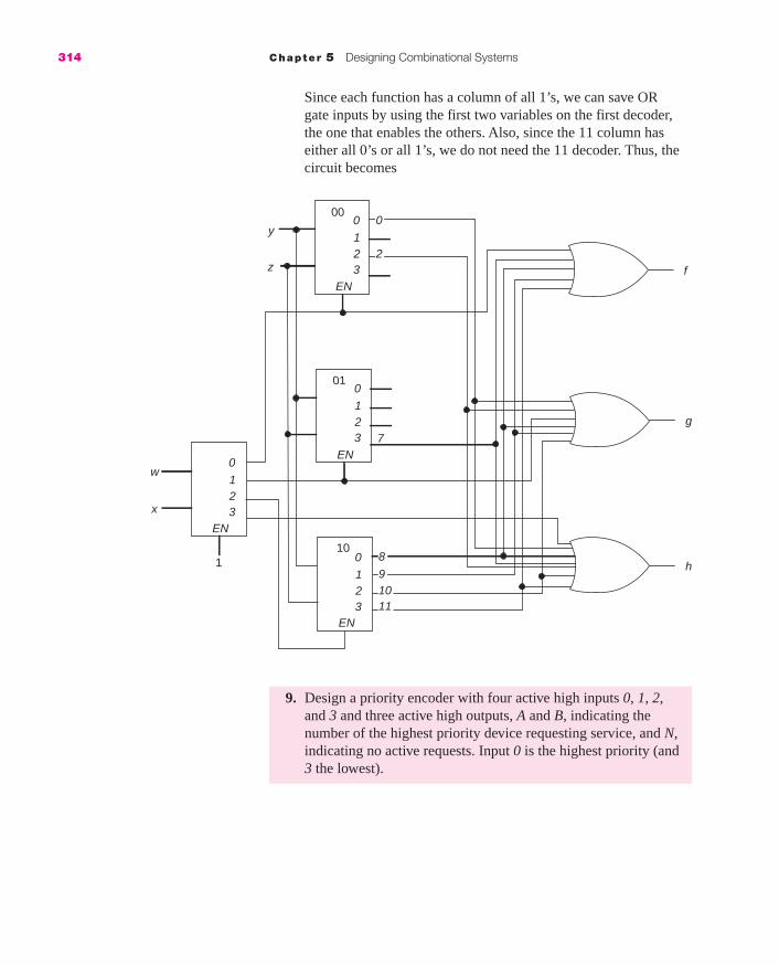
314 Chapter 5 Designing Combinational Systems
9. Design a priority encoder with four active high inputs 0, 1, 2,and 3 and three active high outputs, A and B, indicating thenumber of the highest priority device requesting service, and N,indicating no active requests. Input 0 is the highest priority (and3 the lowest).
EN
w
x
y
z
EN
EN
01
10
0
123
ENf
00
g
h
0
2
7
8
91011
0
123
0
123
0
123
1
Since each function has a column of all 1’s, we can save ORgate inputs by using the first two variables on the first decoder,the one that enables the others. Also, since the 11 column haseither all 0’s or all 1’s, we do not need the 11 decoder. Thus, thecircuit becomes
mar91647_c05b_286_318.qxd 11/14/08 12:17 PM Page 314

5.9 Solved Problems 315
0 1 2 3 A B N
0 0 0 0 X X 11 X X X 0 0 00 1 X X 0 1 00 0 1 X 1 0 00 0 0 1 1 1 0
N is clearly just
N � 0� 1� 2� 3�
We can map A and B to obtain
A � 0� 1�
B � 0� 1 � 0� 2�
00 01 11 10
00
01
11
10
0 1
1
1
1
1
X
1
2 3
B
00 01
A
11 10
00
01
11
10
0 1
X
1
1
1
2 3
10. We have four 3-bit numbers: w2 � w0, x2 � x0, y2 � y0, and z2 � z0. We want to select one of these, based on the input s andt (where st � 00 selects w, st � 01 selects x, and so forth). Theanswer is to appear on output lines f2 � f0. Use the 74153 multiplexer chip to do this.
mar91647_c05b_286_318.qxd 11/14/08 12:17 PM Page 315

316 Chapter 5 Designing Combinational Systems
GA 1 5 3
S1 S0
S1 S0
GB
A3A2A1A0
B3B2B1B0
YA f2
f1YB
w2x2
y2z2
w1x1
y1z1
GA 1 5 3
GB
A3A2A1A0
0
0
0
0
B3B2B1B0
YA f0
not usedYB
w0x0
ts
y0z0
not used
11. Create an eight-way multiplexer using some of the 2-way multi-plexers of Figure 5.11.
We build two 4-way multiplexers as in Figure 5.12b and use athird layer of multiplexer to switch those two outputs. AssumeS2 is the high-order select bit.
The 74153 contains two 4-way multiplexers. Since we needthree, we will use two such circuits as shown below. Note thatone-half of the second 74153 is unused.
mar91647_c05b_286_318.qxd 11/14/08 12:17 PM Page 316

5.9 Solved Problems 317
S2
out
e
f
g
h
S0
a
b
c
d
S1
S1
12. Implement the function
f (w, x, y, z) = �m(0, 1, 5, 7, 8, 10, 13, 14, 15)
a. Using two 8-way multiplexers with an active low enable, plusan OR gate
b. Using one 8-way multiplexer
a. We will enable the first multiplexer if w � 0 and the second if w � 1. Thus, the inputs to the first correspond to the first eightminterms, and those to the second correspond to the second eight.
1
1
1
1
0
0
0
0
w
x y z
1
1
0
1
1
0
0
1
w �
x y z
f
mar91647_c05b_286_318.qxd 11/14/08 12:17 PM Page 317

318 Chapter 5 Designing Combinational Systems
b. We can construct an 8-line truth table with columns for w� andw. Finally, we add a column that is a function of w.
f f
x y z w = 0 w = 1
0 0 0 1 1 10 0 1 1 0 w�0 1 0 0 1 w0 1 1 0 0 01 0 0 0 0 01 0 1 1 1 11 1 0 0 1 w1 1 1 1 1 1
That produces the circuit (with no need for an enable):
13. For the three functions of four variables shown on the mapsbelow,
a. Implement it with the ROM.
b. Find a minimum cost two-level NAND circuit (whereminimum cost is minimum number of gates, and amongthose with the same number of gates, minimum numberof gate inputs). Assume all inputs are available bothcomplemented and uncomplemented. (Minimum is10 gates.)
c. Implement with a PAL similar to the one in the text.
d. Implement it with the PLA with eight product terms available(less may be used).
1
1
w �
1
w
0
0
w
f
x y z
mar91647_c05b_286_318.qxd 11/14/08 2:14 PM Page 318

5.9 Solved Problems 319
a. For the ROM, we need a list of minterms, namely,
X(A, B, C, D) � �m(1, 3, 5, 7, 8, 9, 11)
Y(A, B, C, D) � �m(0, 2, 4, 5, 7, 8, 10, 11, 12)
Z(A, B, C, D) � �m(1, 2, 3, 5, 7, 10, 12, 13, 14, 15)
We can then complete the ROM diagram below.
A B C D
X
0
1
2
3
4
5
6
7
8
9
10
11
12
13
14
15
Y Z
X Y Z
00 01 11 10
00
01
11
10
A BC D
11 1
1
11 1
00 01 11 10
00
01
11
10
A BC D
1
1111
1
1 1
1
00 01 11 10
00
01
11
10
A BC D
11 1
1
11
1 11
1
mar91647_c05c_319_364.qxd 11/14/08 10:23 AM Page 319

where the terms circled in brown and gray are shared. Theresulting equations are
X � A�D � AB�C� � AB�CD
Y � C�D� � A�BD � B�CD� � AB�CD
Z � A�D � AB � B�CD�
The resulting circuit is
320 Chapter 5 Designing Combinational Systems
Y
A�BD
C�
D
B�C ZD�
A
B
AB�
A�
XD
AB�CD
C�
b. The maps below show the minimum cost two-level solution.
00 01 11 10
00
01
11
10
A BC D
11 1
1
11 1
00 01 11 10
00
01
11
10
A BC D
1
1111
1
1 1
1
00 01 11 10
00
01
11
10
A BC D
11 1
1
11
1 11
1
mar91647_c05c_319_364.qxd 11/14/08 10:23 AM Page 320

5.9 Solved Problems 321
c. For the PAL, nothing is gained by treating this as a multipleoutput problem. Thus, the equations we get solving eachfunction individually are implemented.
X � B�D � A�D � AB�C�
Y � C�D� � B�D� � A�BD � AB�C
Z � AB � A�D � B�CD�
A B C D
X
Y
Z
Two of the inputs are not used; the fourth output is not shown.AND gates that are not used have D and D� connected to theirinputs to produce a 0 output.
d. For the PLA, we also need sum of products expressions, butare limited to eight terms. The solution used for part c usesnine terms. We could use B�CD� (which is required for Z ) inplace of B�D� in Y, or we could use the solution to part b; thatsolution is shown on the next page.
mar91647_c05c_319_364.qxd 11/14/08 10:23 AM Page 321
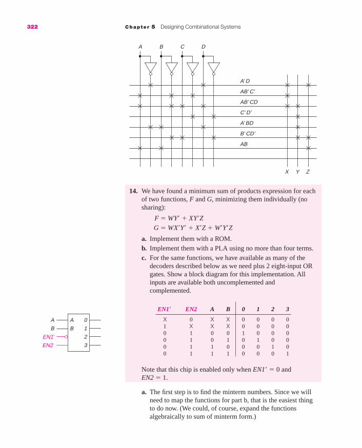
14. We have found a minimum sum of products expression for eachof two functions, F and G, minimizing them individually (nosharing):
F � WY� � XY�Z
G � WX�Y� � X�Z � W�Y�Z
a. Implement them with a ROM.
b. Implement them with a PLA using no more than four terms.
c. For the same functions, we have available as many of thedecoders described below as we need plus 2 eight-input ORgates. Show a block diagram for this implementation. Allinputs are available both uncomplemented andcomplemented.
A B C D
X
A�D
AB�C�
AB�CD
C�D�
A�BD
B�CD�
AB
Y Z
322 Chapter 5 Designing Combinational Systems
EN1� EN2 A B 0 1 2 3
X 0 X X 0 0 0 01 X X X 0 0 0 00 1 0 0 1 0 0 00 1 0 1 0 1 0 00 1 1 0 0 0 1 00 1 1 1 0 0 0 1
0
1
2
3
A
B
A
B
EN2
EN1�
Note that this chip is enabled only when EN1� � 0 andEN2 � 1.
a. The first step is to find the minterm numbers. Since we willneed to map the functions for part b, that is the easiest thingto do now. (We could, of course, expand the functionsalgebraically to sum of minterm form.)
mar91647_c05c_319_364.qxd 11/14/08 10:23 AM Page 322

5.9 Solved Problems 323
From this, we get
F(W, X, Y, Z) � �m(5, 8, 9, 12, 13)
G(W, X, Y, Z) � �m(1, 3, 5, 8, 9, 11)
This produces the following ROM diagram:
W X Y Z
F
0
1
2
3
4
5
6
7
8
9
10
11
12
13
14
15
G
F G
00 01 11 10
00
01
11
10
W XY Z
1 1 1
11
00 01 11 10
00
01
11
10
W XY Z
11 1
1
1 1
mar91647_c05c_319_364.qxd 11/14/08 10:23 AM Page 323

b. For the PLA, we need to find a sum of products solution thatuses only four different terms. The maps below show such asolution.
The PLA below implements this four-term solution.
c. The straightforward approach is to use W and X to enableeach of four decoders. However, looking at the maps, we seethat the last row of each map contains no 1’s. If we use Y andZ to enable the decoders, we only need three, enabled on 00,
W X Y Z
F
W Y�
W� X Y� Z
X� Z
W X� Y�
G
F
F � W Y� � W� X Y� ZG � X� Z � W X� Y� � W� X Y� Z
G
00 01 11 10
00
01
11
10
W XY Z
1 1 1
11
00 01 11 10
00
01
11
10
W XY Z
11 1
1
1 1
324 Chapter 5 Designing Combinational Systems
mar91647_c05c_319_364.qxd 11/14/08 10:23 AM Page 324

5.9 Solved Problems 325
01, and 11. The first decoder has active outputs for all of theminterms that end in 00, that is, 0, 4, 8, and 12. The circuitthen becomes
15. Design a 1-bit decimal adder, where decimal digits are stored inexcess 3 code.
When you add the two codes using a binary adder, the carry isalways correct. The sum must be corrected by adding �3 ifthere is no carry or �3 if there is a carry.
0011 0 1010 7
0100 1 1001 6
0 0111 1 0011
�3 1101 +3 0011
(1) 0100 1 0110 13
0
1
28
123
A
B
W
X
Y
EN2
EN1�
Z �
0
1
29
5
1
133
A
B
W
X
Y
EN2
EN1�
Z
0
1
211
3
3
A
B
W
X
Y �
EN2
EN1�
Z
F
G
mar91647_c05c_319_364.qxd 11/14/08 10:23 AM Page 325

326 Chapter 5 Designing Combinational Systems
Excess 3 2 of 5Digit wxyz abcde
0 0011 110001 0100 101002 0101 100103 0110 100014 0111 011005 1000 010106 1001 010017 1010 001108 1011 001019 1100 00011
16. We have two different codes for the decimal digits that wesometimes use—the excess 3 code and the 2 of 5 code, shownbelow.
4-Bit Adder
4-Bit Adder
A�s B�s
s4s3s2s1
cin
cout
sumignored
c
01
mar91647_c05c_319_364.qxd 11/14/08 10:23 AM Page 326

5.9 Solved Problems 327
All other combinations of input bits never occur. We wish tobuild a box that converts excess 3 code to 2 of 5 code. It thushas four inputs—w, x, y, and z—and has five outputs—a, b, c, d,and e. All inputs are available both complemented anduncomplemented.
a. Map each of the five functions and find all minimum sum ofproducts and product of sums solutions for each of the fivefunctions individually.
b. Our building blocks consist of integrated circuit chips. We canbuy any of the following chips:
7404: 6 inverters7400: 4 two-input NAND gates 7402: 4 two-input NOR gates7410: 3 three-input NAND gates 7427: 3 three-input NOR gates7420: 2 four-input NAND gates 7425: 2 four-input NOR gates
All chips cost the same, 25¢ each.Find one of the least expensive ($1.25) implementations
of the five outputs. (The gates on any chip may be used aspart of the implementation of more than one of the outputs.)Show the algebraic expression and the block diagram for thesolution.
c. Find three solutions, one of which uses only 7400 and 7410packages, one of which uses 7420s also (it must use at leastone four-input gate), and a solution that uses only NOR gates.Each of these must cost no more than $1.25. (Of course, oneof these is the solution to part b.)
d. Implement this with a ROM.
e. Implement this with a PLA.
a. The maps of the five functions and their complements areshown next.
mar91647_c05c_319_364.qxd 11/14/08 10:23 AM Page 327
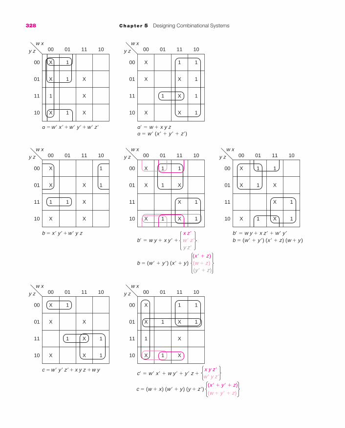
328 Chapter 5 Designing Combinational Systems
00 01 11 10
00
01
11
10
w x
a � w � x � � w � y � � w � z� a� � w � x y za � w � (x � � y � � z�)
y z
1X X
1X
1
X 1 X
X
00 01 11 10
00
01
11
10
w xy z
X X 1
11X
1 X
X X 1
1
10
1
1
b � x� y� � w � y z b� � w y � x z� � w� y �
b � (w � � y �) (x � � z) (w � y ) x z�
b� � w y � x y � � w � z�
y z�
00 01 11
00
01
11
10
w xy z
1X X
11X
X X1
X
00 01 11 10
00
01
11
10
w xy z
X X1
11X
X
X X 11
1
00 01 11 10
00
01
11
10
w xy z
1X X
1X
1 1
X X
X
(x � � z)b � (w � � y �) (x � � y ) (w � z) (y � � z)
00 01 11 10
00
01
11
10
w xy z
X X
1X
11
X X 1
X
00 01 11 10
00
01
11
10
w xy z
X X1 1
1 1X
X
X X1
1
c � w � y � z� � x y z � w y
c � (w � x) (w � � y ) (y � z�)(x � � y � � z)
(w � y � � z)
x y z�
w � y z�c� � w � x� � w y � � y � z �
mar91647_c05c_319_364.qxd 11/14/08 10:23 AM Page 328

5.9 Solved Problems 329
10
1
1
00 01 11
00
01
11
10
w xy z
X X
1X
X X1
X
11 10
X
1
X
X 1
00 01
00
01
11
10
w xy z
X 1
1X
X
1 1
e� � x� z� � w � y � � w � ze � (x � z) (w � y ) (w � z�)
e � w z � w x �
10
1
00 01 11
00
01
11
10
w xy z
X X
1X
X
X X1
1 1 1
d� � w � z� � x � z � x yd � (w � z) (x � z�) (x � � y �)
00 01 11 10
00
01
11
10
w xy z
1X X
1X
X X1
X 111
00 01 11 10
00
01
11
10
w xy z
1X X
11X
X X 1
X
d � w z� �x y � zw � y � z
d � (w � z )
x � zw zd� � w� z� �
w� yy z
(x � z�)(w � � z�)
(w � y �)(y � � z�)
�
w � y z�
x y z�
Note that there are two SOP solutions for d and e, and thatthere are four POS solutions for b, two for c, and five for d.
b. If we were to use the solutions that we found in part a, thereare no common product terms and thus no sharing is possiblein the NAND gate implementation. We would need 10 two-input gates and 8 three-input gates, for a total of three 7400sand three 7410s (at a total cost of $1.50). For the NOR gatesolution, we would use the product of sums. There is onlyone term that can be shared, w � y, in b and e. There wouldbe a total of 1 four-input gate, 5 three-input gates, and12 two-input gates, once again requiring six integrated circuitpackages.
We must then attempt to do sharing. The following mapsshow that for the sum of product solutions.
mar91647_c05c_319_364.qxd 11/14/08 10:23 AM Page 329

330 Chapter 5 Designing Combinational Systems
10
1
00 01 11
00
01
11
10
w xy z
X X
1 1X
X X 1
X
11 10
X
X
X1
00 01
00
01
11
10
w xy z
X 1
1X
X
1
d e
a
10
1
00 01 11
00
01
11
10
w xy z
X X
1X
X
X X
1 1
00 01 11 10
00
01
11
10
w xy z
X X
1X
X X 1
X 11
00 01 11 10
00
01
11
10
w xy z
1X X
1X
X X1
X1
b c
a � w � x� � x y � z � w � z�
b � x� y � � w � x� � x y zc � w � y � z� � x y z � w yd � w z� � x y � ze � w z � w x � w � y z�
In this solution, three terms have been shared (as indicatedby the colored circling and terms). There are some otherchoices (w�y�z in place of xy�z in a and d, and xyz� inplace of w�yz� in e), but they would not alter the gatecount. This solution requires 8 two-input gates and 8 three-input gates and utilizes two 7400s and three 7410s (totalcost $1.25).
c. The solution to part b could be used as one of the threesolutions to part c, and any of those shown here could havebeen used for part b. A solution that requires one less newproduct term is
a � w�x� � xy�z � w�y�z� � w�yz�
where the last two terms are required for (and shared with)c and e, respectively. This saves 1 two-input gate, butreplaces a three-input gate with a four-input one (all in theimplementation of a). This solution requires 1 four-inputgate and 7 each of three-input and two-input gates. It utilizes
mar91647_c05c_319_364.qxd 11/14/08 10:23 AM Page 330

5.9 Solved Problems 331
one 7420, two 7430s (using the extra four-input gate for theseventh three-input one) and two 7400s (total cost $1.25).
There is also a solution using NOR gates, based on theproduct of sums solutions. The maps of the complementsbelow produce one solution that almost works:
10
1
00 01 11
00
01
11
10
w xy z
X X
11X
X
X X1 1
1
00 01 11 10
00
01
11
10
w xy z
X X1 1
1 1X
X X1
X1
00 01 11 10
00
01
11
10
w xy z
1X X
1 1X
X X 1
X1 1
10
1
00 01 11
00
01
11
10
w xy z
X X
1X
X X1
X11 1
11 10
X
X
X 1
00 01
00
01
11
10
w xy z
X 1
11X
X
11
a b
d e
c
a � w�(x� � y� � z�)
b � (x� � y)(w� � y�)(w � y� � z)
c � (w � x)(w� � y)(y � z�)(w � y� � z)
d � (w � z)(x � z�)(x� � y� � z�)
e � (x � z)(w � y)(w � z�)
This solution requires 1 four-input gate, 5 three-input gates,and 11 two-input gates (utilizing six packages).
However, if we do not restrict ourselves to two-levelsolutions, we could eliminate the four-input gate, by rewritingc as
c � (w � x)(y � w�z�)(w � y� � z)
mar91647_c05c_319_364.qxd 11/14/08 10:23 AM Page 331

332 Chapter 5 Designing Combinational Systems
Now, the gate count becomes 6 three-input gates and10* two-input gates (utilizing five packages). (Similarmanipulation could be done on e, replacing a three-inputgate by a two-input one, but that would not change thepackage count.) A block diagram of the circuit is shownbelow.
d, e. The implementation with a ROM and a PLA arerather straightforward. For the ROM, all we need isthe minterms; the don’t cares are ignored. For the PLA,any of the sum of product solutions can be used, as longas we have enough terms. The two solutions are shownbelow.
c
aw
y
w
x
w
z
x�
z�y�
w
zy�
x
z�d
e
x
z
w
y
w
z�
b
x�
y
w�
y�
*By doing this, we have saved a two-input gate, since the term w�z� uses the same NORgate as the term w � z.
mar91647_c05c_319_364.qxd 11/14/08 10:23 AM Page 332

e.
5.9 Solved Problems 333
d. w x y z
a
0
1
2
3
4
5
6
7
8
9
10
11
12
13
14
15
cb ed
17. Design a controller to display an electronic nine-dotted die asshown next. A set of these could be used to display decimalnumbers and some mathematical equations.
w x y z
a
w�x�
x y�z
w�z�
x�y�
x y z
w�y�z�
wy
wz�
wz
wx
w�yz �
cb ed
mar91647_c05c_319_364.qxd 11/14/08 10:23 AM Page 333

334 Chapter 5 Designing Combinational Systems
The inputs to the controller represent a 4-bit number, W, X,Y, Z, which indicates what is to be displayed. They are allavailable both uncomplemented and complemented. There arenine outputs, A, B, C, D, E, F, G, H, J, one for each of the dots.
The display comes in two types. The first type requires a 1 tolight the display. The second type requires a 0 to light the display.For the second version, the outputs of the controller are thecomplement of the outputs required for the first type of display.
The diagram below shows each of the inputs and thedisplay that results. A black dot indicates that the bit is lit; acircle indicates not lit. Note that 0 lights none of the lights;9 lights all of them.
a. Show the truth table for the controller.
b. Write a minimum sum of products expression for each of theoutputs, treating each output as a separate problem. Showboth maps and algebraic expressions. For each expression,
00000
01015
1010�
00011
01106
1011�
00102
01117
1100.
decimalpoint
00113
10008
1101�
01004
10019
Other combinations(1110, 1111)will never occur.
A
D
B C
E F
G H J
mar91647_c05c_319_364.qxd 11/14/08 10:23 AM Page 334

5.9 Solved Problems 335
all terms must be prime implicants of that function. Sharingis possible only if a product term is a prime implicant ofmore than one function.
c. Assume that the functions found in part b are to beimplemented with a two-level NAND gate circuit. Do notbuild two gates with the same inputs. How many two-inputand how many three-input gates are used? (No gates may beused as NOT gates; there is no need for any gates with morethan three inputs.) If 7400 and 7410 integrated circuitpackages were used, how many of each are used?
d. Show the equations and a block diagram of a minimum costtwo-level NAND gate implementation. (Of course, there willbe sharing, and some of the terms will not be prime implicantsof one or more of the functions for which they are used.) Nogates may be used as NOT gates. How many integrated circuitpackages are needed?
e. We went to implement this but ran into a problem. All wecould find was one 7410 package of three-input NAND gates(three gates in the package). There were plenty of 7400packages of two-input gates. Show the equations and a blockdiagram for an implementation this way. No gates may beused as NOT gates. (It is possible to start with either thesolution to part b or d above, or some other set of equations.)Use as few 7400s as possible.
a. The truth table for the controller with active high outputs isshown below. (In the output columns of the version withactive low outputs, there would be 0’s where this one has 1’sand 1’s where this has 0’s. The don’t cares would be thesame.)
W X Y Z A B C D E F G H J
0 0 0 0 0 0 0 0 0 0 0 0 00 0 0 1 0 0 0 0 1 0 0 0 00 0 1 0 1 0 0 0 0 0 0 0 10 0 1 1 1 0 0 0 1 0 0 0 10 1 0 0 1 0 1 0 0 0 1 0 10 1 0 1 1 0 1 0 1 0 1 0 10 1 1 0 1 0 1 1 0 1 1 0 10 1 1 1 1 0 1 1 1 1 1 0 11 0 0 0 1 1 1 1 0 1 1 1 11 0 0 1 1 1 1 1 1 1 1 1 11 0 1 0 0 1 0 1 1 1 0 1 01 0 1 1 0 0 0 1 1 1 0 0 01 1 0 0 0 0 0 0 0 0 0 0 11 1 0 1 0 0 0 1 1 1 1 1 11 1 1 0 X X X X X X X X X1 1 1 1 X X X X X X X X X
mar91647_c05c_319_364.qxd 11/14/08 10:23 AM Page 335
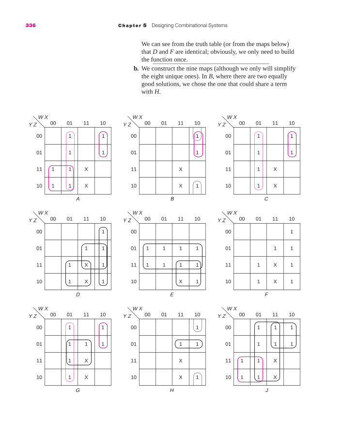
336 Chapter 5 Designing Combinational Systems
A
1000 01 11
00
01
11
10
W XY Z
1
1
X
1X
00 01 11 10
00
01
11
10
W XY Z
1 1
1 1
1 X
X1
00 01 11 10
00
01
11
10
W XY Z
1
1
X1
X1
1
1
1
1
B C
D
1000 01 11
00
01
11
10
W XY Z
1
1X
00 01 11 10
00
01
11
10
W XY Z
1
1
1
1X
X 1
1
1
00 01 11 10
00
01
11
10
W XY Z
1 1
1
1
1
X 1
X 1
1
1
1 1
1
1
1
E F
G
1000 01 11
00
01
11
10
W XY Z
1
1 1
X
1X
00 01 11 10
00
01
11
10
W XY Z
1
1
1
1
1
X
X
1
1 1
1 1
00 01 11 10
00
01
11
10
W XY Z
1 1
1
1
1
X1
X1
H J
We can see from the truth table (or from the maps below)that D and F are identical; obviously, we only need to buildthe function once.
b. We construct the nine maps (although we only will simplifythe eight unique ones). In B, where there are two equallygood solutions, we chose the one that could share a termwith H.
mar91647_c05c_319_364.qxd 11/14/08 10:23 AM Page 336

The equations for the eight functions are
A � W�X � W�Y � WX�Y�
B � WX�Y� � WX�Z�
C � W�X � WX�Y�
D � XY � WX� � WZ
E � Z � WY
G � W�X � WX�Y� � XZ
H � WX�Z� � WY�Z
J � X � WY� � W�Y
c. Note that there are four terms that are shared. This solutionrequires 12 two-input gates and 7 three-input gates (three7400s and three 7410s).
b, c. The maps for the complementary outputs are shown next.The equations for this active low controller (where we areimplementing the complements) are
A� � W�X�Y� � WX � WY
B� � W� � X � YZ
C� � WX � WY � W�X�
D� � W�X� � W�Y� � WXZ�
E� � Y�Z� � W�Z�
G� � WY � W�X� � WXZ�
H� � W� � YZ � XZ�
J� � W�X�Y� � WY
They require 10 two-input gates and 8 three-input gates(three 7400s and three 7410s). There is a lot more sharing,but still six integrated circuit packages are required.
5.9 Solved Problems 337
mar91647_c05c_319_364.qxd 11/14/08 10:23 AM Page 337
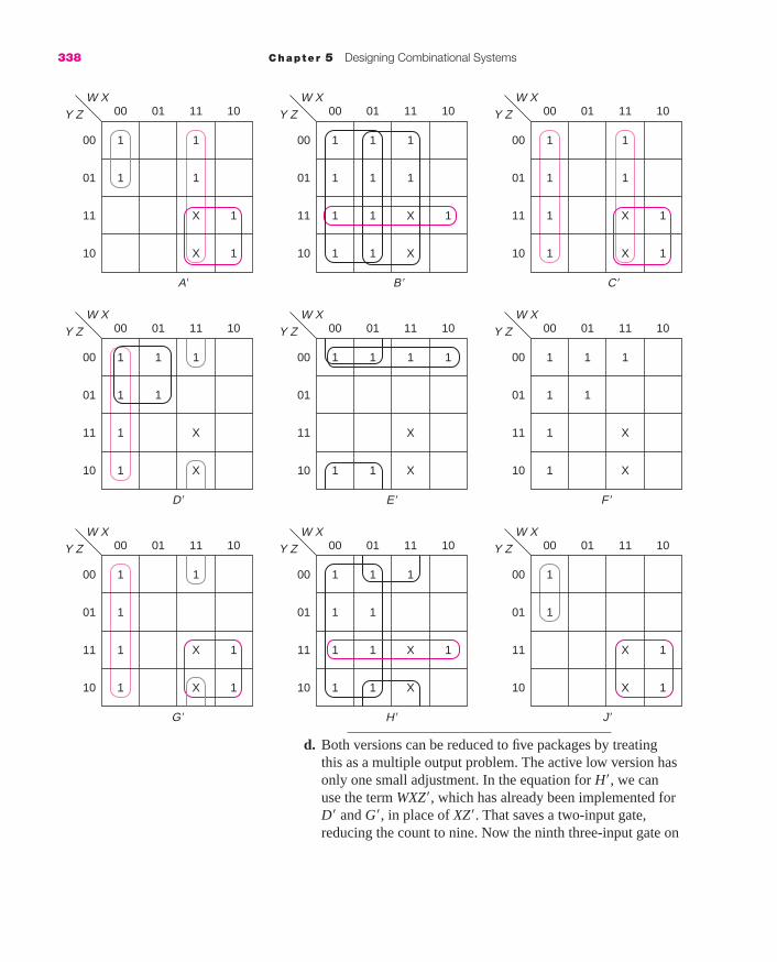
338 Chapter 5 Designing Combinational Systems
d. Both versions can be reduced to five packages by treatingthis as a multiple output problem. The active low version hasonly one small adjustment. In the equation for H�, we canuse the term WXZ�, which has already been implemented forD� and G�, in place of XZ�. That saves a two-input gate,reducing the count to nine. Now the ninth three-input gate on
A�
1000 01 11
00
01
11
10
W XY Z
1 1 1
1 1 1
X
1 1 X
1 1 1
00 01 11 10
00
01
11
10
W XY Z
1 1
1 1
1 X 1
X 11
00 01 11 10
00
01
11
10
W XY Z
1 1
11
X 1
X 1
B� C�
D�
1000 01 11
00
01
11
10
W XY Z
1 1 1 1
X
1 1 X
00 01 11 10
00
01
11
10
W XY Z
1
1 1
1
1
1 X
X1
00 01 11 10
00
01
11
10
W XY Z
1 1
1 11
X1
X1
E� F �
G�
1000 01 11
00
01
11
10
W XY Z
1 1 1
X
1 1
1 1
1
1
1
X
00 01 11 10
00
01
11
10
W XY Z
1
1
1X
X 1
00 01 11 10
00
01
11
10
W XY Z
1
11
X1
X1
1
1
H� J�
mar91647_c05c_319_364.qxd 11/14/08 10:23 AM Page 338

5.9 Solved Problems 339
the 7410 packages can be used as a two-input gate and onlytwo 7400s are needed.
For the active high version, a considerable amount ofsharing can be achieved. The maps for a minimum solutionare shown below.
A
00 01 11 10
00
01
11
10
W XY Z
1 1
11
X11
X11
B
00 01 11 10
00
01
11
10
W XY Z
1
1
X 1
X
C
00 01 11 10
00
01
11
10
W XY Z
11
11
X1
X1
D
00 01 11 10
00
01
11
10
W XY Z
1 1
1
X1 1
X1 1
E
00 01 11 10
00
01
11
10
W XY Z
1111
X 1
X11 1
F
00 01 11 10
00
01
11
10
W XY Z
11
1
X1 1
X1 1
G
00 01 11 10
00
01
11
10
W XY Z
11 1
11
X1
X1
H
00 01 11 10
00
01
11
10
W XY Z
1
1
1
X 1
X
J
00 01 11 10
00
01
11
10
W XY Z
111
111
X11
X11
mar91647_c05c_319_364.qxd 11/14/08 10:23 AM Page 339
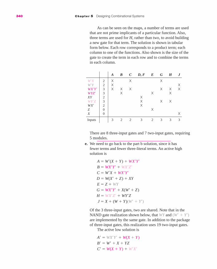
As can be seen on the maps, a number of terms are usedthat are not prime implicants of a particular function. Also,three terms are used for H, rather than two, to avoid buildinga new gate for that term. The solution is shown in tabularform below. Each row corresponds to a product term; eachcolumn to one of the functions. Also shown is the size of thegate to create the term in each row and to combine the termsin each column.
A B C D, F E G H J
W�X 2 X X XW�Y 2 X XWX�Y� 3 X X X X X XWYZ� 3 X X XXY 2 XWY�Z 3 X X XWX� 2 XZ 0 XX 0 X
Inputs 3 2 2 3 2 3 3 3
There are 8 three-input gates and 7 two-input gates, requiring5 modules.
e. We need to go back to the part b solution, since it hasfewer terms and fewer three-literal terms. An active highsolution is
A � W�(X � Y ) � WX�Y�
B � WX�Y� � WX�Z�
C � W�X � WX�Y�
D � W(X� � Z) � XY
E � Z � WY
G � WX�Y� � X(W� � Z )
H � WX�Z� � WY�Z
J � X � (W � Y )(W� � Y�)
Of the 3 three-input gates, two are shared. Note that in theNAND gate realization shown below, that WY and (W� � Y�)are implemented by the same gate. In addition to the packageof three-input gates, this realization uses 19 two-input gates.
The active low solution is
A� � WX�Y� � W(X � Y )
B� � W� � X � YZ
C� � W(X � Y ) � W�X�
340 Chapter 5 Designing Combinational Systems
mar91647_c05c_319_364.qxd 11/14/08 1:50 PM Page 340

5.9 Solved Problems 341
D� � W�X� � (W� � XZ�)(W � Y�)
E� � Y�Z� � W�Z�
G� � W(Y � XZ�) � W�X�
H� � W� � (X � Z)(Y � Z�)
J� � WX�Y� � WY
It uses seven modules. The circuits are shown below.
AWX�Y�
W�
X�
Y�
JW�
Y�
Z�
X�
W
Y
DX
Y
W
X
Z�
G
E
XW
Z�
WX�Z�
B
W�
X
C
WY�Z
H
A�WX�Y�
WX�
W
X�
Y�
W�
X�
X
Z�
B�Y
Z
E�W�
Z�
Y�
Z�
W�
Y
W
C�
W
Y
J�
D�
Y�
ZW
X�
Z�
H �
WY�
G�
mar91647_c05c_319_364.qxd 11/14/08 2:01 PM Page 341

18. You are to design a driver for an eight-segment display asdescribed below. It has four inputs, a, b, c, d and eight outputs,X1, . . . , X8.
This is to display the decimal equivalent of a 4-bit binarynumber that is in one’s complement format. In one’scomplement, the following values are coded:
0000 0 1000 �70001 1 1001 �60010 2 1010 �50011 3 1011 �40100 4 1100 �30101 5 1101 �20110 6 1110 �10111 7 1111 0
(Note that the minus sign (X8) is lit for �1 to �7, but not foreither 0 or for 1 to 7.) Segment X1 may or may not be lit for thedigit 6; segment X6 is not lit for digit 7. All inputs are availableboth complemented and uncomplemented.
a. Show the maps, equations, and a block diagram for aminimum two-level NAND gate solution that treats this aseight separate problems and uses only prime implicants ofeach of the functions. However, the gate implementationshould share gates whenever possible. (Minimum is 36 gates,107 inputs.)
b. Show the maps, equations, and a block diagram for aminimum two-level NAND gate solution—but this time gatesare to be shared wherever possible. Restriction: There are nogates with more than eight inputs. Also, indicate how manymodules you have used.
c. X4 requires at least eight terms and thus an eight-inputNAND gate for a two-level solution. Find a minimumsolution for X4 that uses only two-input gates. (This must,of course, be more than two levels.) Note: This part hasnothing to do with part b. No gate may be used as a NOT.
X1
X7
X4
X2X6
X8
X5 X3
342 Chapter 5 Designing Combinational Systems
mar91647_c05c_319_364.qxd 11/14/08 1:50 PM Page 342

5.9 Solved Problems 343
d. Implement these functions using a PLA with as few terms aspossible. Show a PLA diagram.
a. All but X3 and X7 have unique solutions. There are sixsolutions for X3, the first three of which can share two termswith other solutions. The maps for one of the best solutions,requiring 36 gates and 107 gate inputs, are shown on the nextpage. Shared terms are in brown. The list of solutions is givenbelow. The underlined subscripted terms are shared in thissolution. Other terms that could be shared in a differentsolution are underlined:
X1 � b�d� � bd � ac�7 � a�c
X2 � a�b� � ab � c�d�6 � cd
X3 � ab�5 � c�d�6 � a�d � bc
� ab� � bd� � cd � a�c�
� a�b � cd � ad� � b�c�
� b�d � c�d� � a�b � ac
� a�c� � ad� � b�d � bc
� b�c� � ac � bd� � a�d
X4 � a�b�d�4 � b�cd� � a�b�c � a�cd�3 � abc� � abd2
� bc�d � ac�d1
X5 � ac�d1 � abd 2 � a�cd�3 � a�b�d�4X6 � a�c�d�� a�bc� � a�bd� � ab�d � ab�c � acd
X7 � bc� � b�c � {a�cd�3 or a�bd�} � {ac�d1 or ab�d}
X8 � ab�5 � ac�7 � ad'
The gate count for this solution is
X1: 2 2 2 2 4
X2: 2 2 2 2 4
X3: 2 (2) 2 2 4
X4: 3 3 3 3 3 3 3 3 8
X5: (3) (3) (3) (3) 4
X6: 3 3 3 3 3 3 6
X7: 2 2 (3) (3) 4
X8: (2) (2) 2 3
2�s: 14 7430s: 2 36 gates/107 inputs
3�s: 15 7420s: 3
4�s: 5 7410s: 5
6�s: 1 7400s: 4
8�s: 114 chips
mar91647_c05c_319_364.qxd 11/14/08 1:50 PM Page 343

00 01 11 10
00
01
11
10
a bc d
X1 X2
X
11★ 1★
1
1★1★
1
X
1★
1★
1
00 01 11 10
00
01
11
10
a bc d
1★1 1★ 1
1★
1★
1
1★
1
1★
1★1★
00 01 11 10
00
01
11
10
a bc d
X3 X4
1
11 1 1
1
1
1
1
1
1
1
1
1
00 01 11 10
00
01
11
10
a bc d
1★
1★ 1★
1
1★1★
1
1★
1★
1★
00 01 11 10
00
01
11
10
a bc d
X 5 X6
1★
1★
1
1★
1
1★
00 01 11 10
00
01
11
10
a bc d
1★
1★ 1
1★
1★
1
1★
1★
00 01 11 10
00
01
11
10
a bc d
X 7 X8
1
1 1★
1
1★
1
1
1
1
1★
00 01 11 10
00
01
11
10
a bc d
11
1★
1★
1
1★
1
344 Chapter 5 Designing Combinational Systems
mar91647_c05c_319_364.qxd 11/14/08 1:50 PM Page 344
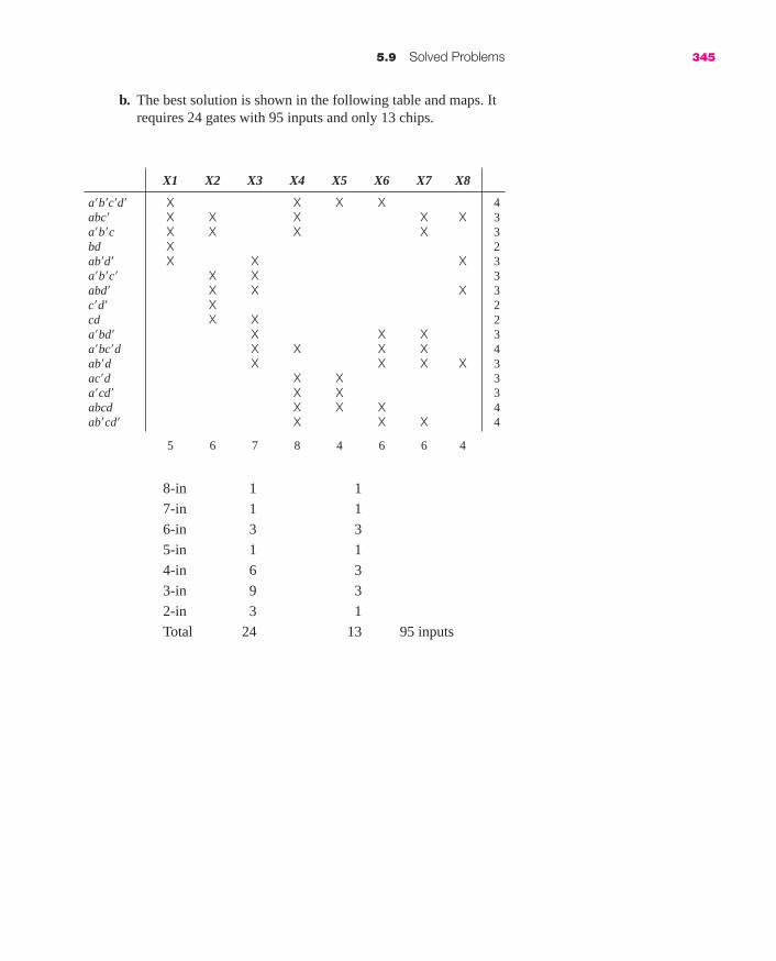
5.9 Solved Problems 345
b. The best solution is shown in the following table and maps. Itrequires 24 gates with 95 inputs and only 13 chips.
8-in 1 1
7-in 1 1
6-in 3 3
5-in 1 1
4-in 6 3
3-in 9 3
2-in 3 1
Total 24 13 95 inputs
X1 X2 X3 X4 X5 X6 X7 X8
a�b�c�d� X X X X 4abc� X X X X X 3a�b�c X X X X 3bd X 2ab�d� X X X 3a�b�c� X X 3abd� X X X 3c�d� X 2cd X X 2a�bd� X X X 3a�bc�d X X X X 4ab�d X X X X 3ac�d X X 3a�cd� X X 3abcd X X X 4ab�cd� X X X 4
5 6 7 8 4 6 6 4
mar91647_c05c_319_364.qxd 11/14/08 1:50 PM Page 345

00 01 11 10
00
01
11
10
a bc d
X1 X2
X
11 1
1
11
1
X
1
1
1
00 01 11 10
00
01
11
10
a bc d
11 1 1
1
1
1
1
1
1
11
00 01 11 10
00
01
11
10
a bc d
X3 X4
1
11 1 1
1
1
1
1
1
1
1
1
1
00 01 11 10
00
01
11
10
a bc d
1
1 1
1
11
1
1
1
1
00 01 11 10
00
01
11
10
a bc d
X 5 X6
1
1
1
1
1
1
00 01 11 10
00
01
11
10
a bc d
1
1 1
1
1
1
1
1
00 01 11 10
00
01
11
10
a bc d
X 7 X8
1
1 1
1
1
1
1
1
1
1
00 01 11 10
00
01
11
10
a bc d
11
1
1
1
1
1
346 Chapter 5 Designing Combinational Systems
mar91647_c05c_319_364.qxd 11/14/08 1:50 PM Page 346

5.9 Solved Problems 347
c.
X4 � a�b�d� � b�cd� � a�b�c � a�cd� � abc� � abd � bc�d � ac�d� a�b�(c � d�) � ab(c� � d) � cd�(a� � b�) � c�d(a � b)� [a� � b(c� � d)][a � b�(c � d�)]
� [c � d(a � b)][c�� d�(a� � b�)]
d. The solution to part b translates directly into a PLA with 16product terms (where each row corresponds to a product term).An equally good solution would be to design the PLA as aROM. It, too, would have 16 terms. (Note: The ROM solutiondoes not work for part b since it would require a 14-input gatefor X3.)
X4
b
b�
b�
d
d�
a
a�
c�
c
c
d�
d
c�
a�
b
a
mar91647_c05c_319_364.qxd 11/14/08 1:50 PM Page 347

5.10 EXERCISES1. For the following circuit:
G
D
E�
D�
C�
E
C
A
E
B
B�
A
a. Compute the maximum delay,
i. Assuming that all inputs are available bothuncomplemented and complemented
ii. Assuming only uncomplemented inputs are available andan additional gate must be added to complement eachinput
b. Compute the maximum delay from input C to the output,assuming that all inputs are available both uncomplementedand complemented.
�2. We are building an adder to add the 32-bit constant
10101010101010101010101010101010
to an arbitrary 32-bit number. We will implement this with 16identical adder modules, each of which will add 2 bits of thenumber to the constant (10) and a carry from the next lower pairof bits and produce 2 bits of the sum and the carry to the next bits. A block diagram of part of this is shown below:
2-bitadder
a bc
sy
t
EX
ER
CIS
ES
348 Chapter 5 Designing Combinational Systems
mar91647_c05c_319_364.qxd 11/14/08 1:50 PM Page 348

5.10 Exercises 349
The problem each 2-bit adder solves is
c
a b
1 0y s t
a. Show a truth table for that 2-bit adder (it has three inputs, a, b,and c, and it has three outputs, y, s, and t), and find minimumSOP expressions for each output.
b. Compute the delay from the c input of each module to the y output of that module and the total delay for the 32 bits.
3. We want to build a circuit to compute the two’s complement ofan n-bit number. We will do this with n modules, each of whichcomplements that bit and then adds the carry from the next lowerbit. Thus, the first three bits of a block diagram of the circuit willlook like
a. Show a block diagram for each of the boxes using NANDgates. (Design the first—on the right—box specially.)
b. Compute the delay for n bits.
c. Improve the speed by designing 2 bits at a time. Show aNAND gate circuit and compute the total delay.
4. We want to build an adder to simultaneously add three multidigitbinary numbers. Design a single bit of that adder. It has threeinputs for that digit, x, y, and z, plus two carry inputs, u and v(since you may have a carry of 0, 1, or 2). There are three outputs,a sum, s, and two carries, f and g. Show a truth table and find theminimum sum of products expressions for the three outputs.
5. Design a circuit to multiply two 2-bit numbers—a, b and c, d andproduce a 4-bit product—w, x, y, z. Show a truth table and theequations.
c2 1c1 c0
a2 a1 a0
b2 b1 b0
EX
ER
CIS
ES
mar91647_c05c_319_364.qxd 11/14/08 1:50 PM Page 349

6. We need to determine whether a three-bit number, a3, a2, a1, isequal to another number, b3, b2, b1, or if it is greater than thatnumber. (We do not need an output for less than.)
a. Show how the 7485 would be connected to accomplish this.
b. Implement this with AND and OR gates.
c. Assuming that the 7485 costs $1, what must 7400 seriesAND and OR gate packages cost to make the AND/ORimplementation less expensive?
�7. Consider the following circuit with an active high output decoder.Draw a truth table for X and Y in terms of a, b, and c.
8. We wish to design a decoder, with three inputs, x, y, z, and eightactive high outputs, labeled 0, 1, 2, 3, 4, 5, 6, 7. There is no enableinput required. (For example, if xyz � 011, then output 3 would be1 and all other outputs would be 0.)
The only building block is a two-input, four-output decoder(with an active high enable), the truth table for which is shownbelow.
Y
Xa
b
c
0
1
2
3
4
5
6
7
Draw a block diagram of the system using as many of thesebuilding blocks as are needed.
�9. We want to implement a full adder; we’ll call the inputs a, b, and cand the outputs s and cout. As always, the adder is described by thefollowing equations:
s(a, b, c) � �m(1, 2, 4, 7)
cout(a, b, c) � �m(3, 5, 6, 7)
To implement this, all we have available are two decoders (asshown below) and two OR gates. Inputs a and b are availableboth uncomplemented and complemented; c is available only
0123
A
EN
B
EN A B 0 1 2 3
0 X X 0 0 0 01 0 0 1 0 0 01 0 1 0 1 0 01 1 0 0 0 1 01 1 1 0 0 0 1
EX
ER
CIS
ES
350 Chapter 5 Designing Combinational Systems
mar91647_c05c_319_364.qxd 11/14/08 1:50 PM Page 350

5.10 Exercises 351
uncomplemented. Show a block diagram for this system. Be sureto label all of the inputs to the decoders.
11. Design, using AND, OR, and NOT gates, a priority encoder withseven active low inputs, 1�, . . . , 7� and three active high outputs,CBA that indicate which is the highest priority line active. Input 1�is highest priority; 7� is lowest. If none of the inputs are active, theoutput is 000. There is a fourth output line, M, which is 1 if thereare multiple active inputs.
12. Implement the function
f (x, y, z) � �m(0, 1, 3, 4, 7)
using two-way multiplexers.
13. In the following circuit, the decoder (DCD) has two inputs andfour (active high) outputs (such that, for example, output 0 is 1if and only if inputs A and B are both 0). The three multiplexerseach have two select inputs (shown on the top of the box), fourdata inputs (shown on the left) and an active high enable input(shown on the bottom). Inputs A, B, C, and D are select inputs;inputs N through Z are data inputs. Complete a truth giving thevalue of F for each of the 16 possible select input combinations.(Comment: For some values, F � 0; for one value, F � W.)
EN� A B 0 1 2 3
1 X X 0 0 0 00 0 0 1 0 0 00 0 1 0 1 0 00 1 0 0 0 1 00 1 1 0 0 0 1
0123
EN �
A
B
10. Show the block diagram for a decoder, the truth table for whichis shown below. The available components are one-, two-, and three-input NAND gates. (A one-input NAND is an inverter.)
Inputs Outputs
E1 E2 a b 1 2 3
0 X X X 1 1 1X 0 X X 1 1 11 1 0 0 1 1 11 1 0 1 0 1 11 1 1 0 1 0 11 1 1 1 1 1 0
�
EX
ER
CIS
ES
mar91647_c05c_319_364.qxd 11/14/08 1:50 PM Page 351

14. The following circuit includes a multiplexer with select inputs,A and B, and data inputs, W, X, Y, and Z:
Write an algebraic equation for F.
15. For the following sets of functions, design a system
i. Using a ROM
ii. Using a PLA with the number of product terms shown
iii. Using a PAL
a. F(A, B, C) � �m(3, 4, 5, 7)
G(A, B, C) � �m(1, 3, 5, 6, 7)
H(A, B, C) � �m(1, 4, 5) (4 product terms)
b. W(A, B, C) � �m(0, 1, 4)
X(A, B, C) � �m(0, 3, 4, 7)
Y(A, B, C) � �m(1, 2, 6)
Z(A, B, C) � �m(2, 3, 6, 7) (4 product terms)
WX
A B
FYZ
NP
C D
QR
ST
C D
UV
WX
C D
YZ
AB
DCD
0123
F
EX
ER
CIS
ES
352 Chapter 5 Designing Combinational Systems
mar91647_c05c_319_364.qxd 11/14/08 1:50 PM Page 352

5.10 Exercises 353
c. f(a, b, c, d ) � �m(3, 5, 6, 7, 8, 11, 13, 14, 15)
g(a, b, c, d ) � �m(0, 1, 5, 6, 8, 9, 11, 13, 14)(6 product terms)
d. F(A, B, C, D) � �m(1, 2, 6, 7, 8, 9, 12, 13)
G(A, B, C, D) � �m(1, 8, 9, 10, 11, 13, 15)
H(A, B, C, D) � �m(1, 6, 7, 8, 11, 12, 14, 15)(8 product terms)
16. We have found a minimum sum of products expression for eachof two functions, F and G, minimizing them individually (nosharing):
F � W�X�Y� � XY�Z � W�Z
G � WY�Z � X�Y�
a. Implement them with a ROM.
b. Implement them with a PLA with four terms.
c. For the same functions, we have available as many of thedecoders described below as are needed plus 2 eight-inputOR gates. Show a block diagram for this implementation. Allinputs are available both uncomplemented and complemented.
AB
EN1�
EN2
0123
EN1� EN2 A B 0 1 2 3
X 0 X X 0 0 0 01 X X X 0 0 0 00 1 0 0 1 0 0 00 1 0 1 0 1 0 00 1 1 0 0 0 1 00 1 1 1 0 0 0 1
Note that this chip is enabled only when EN1� � 0 andEN2 � 1.
17. Consider the following three functions, f, g, and h of the fourvariables, a, b, c, and d, whose minimum solutions (treating eachas a separate problem) are listed below. Throughout, all variablesare available only uncomplemented:
f � b�c�d� � bd � a�cd
g � c�d� � bc� � bd� � a�b�cd
h � bd� � cd � ab�d
a. Implement them with a ROM.
b. Implement them on a PLA with six terms.
c. Implement them using only decoders of the type shown below(as many as needed) and three OR gates (each with as manyinputs as you need). (No other gates are allowed.) Logic 0 andlogic 1 are available.
EX
ER
CIS
ES
mar91647_c05c_319_364.qxd 11/14/08 1:50 PM Page 353

18. We have three functions, X, Y, Z of the four variables, A, B, C, D.Note: Each part can be solved without the other:
X(A, B, C, D) � �m(0, 2, 6, 7, 10, 13, 14, 15)
Y(A, B, C, D) � �m(2, 6, 7, 8, 10, 12, 13, 15)
Z(A, B, C, D) � �m(0, 6, 8, 10, 13, 14, 15)
a. Implement with a two-level NAND gate circuit. This can bedone using only prime implicants of the individual functionswith 13 gates. With sharing, it can be done with 10 gates.Assume that all variables are available both complemented anduncomplemented.
b. Implement these functions using a ROM.
c. Implement this with 2 three-input (plus active low enable)decoders as shown below, plus a minimum number of AND,OR, and NOT gates.
d. Implement it with a PLA with eight terms. (You may not needto use all of them.)
e. Implement them with the PAL shown in the text.
19. Implement the 2-bit adder of Section 5.1.2 using the PAL ofSection 5.6.3. The problem is that one of the output functionsrequires 7 terms and another 12. This can be overcome by buildingthe carry between the 2 bits and using that output as another inputto compute s1 and cout.
20. In Solved Problem 16, we designed a converter from excess 3 to 2 of 5 code. In this exercise, we want to do the reverse, that is
01
4567
23
a
b
c
EN
AB
EN1EN2�
0123
EN1 EN2� A B 0 1 2 3
0 X X X 0 0 0 0X 1 X X 0 0 0 00 1 0 0 1 0 0 00 1 0 1 0 1 0 00 1 1 0 0 0 1 00 1 1 1 0 0 0 1
�
EX
ER
CIS
ES
354 Chapter 5 Designing Combinational Systems
mar91647_c05c_319_364.qxd 11/14/08 1:50 PM Page 354

design a converter from 2 of 5 code to excess 3. There will be fourfunctions of five variables. We will assume that only legitimatedigit codes are input; thus, there will be 22 don’t cares on eachmap. All inputs are available both uncomplemented andcomplemented.
a. Map each of the four functions and find all minimum sum ofproducts and product of sums solutions for each of the fourfunctions individually.
b. Our building blocks consist of integrated circuit chips. We canbuy any of the following chips:
7404: 6 inverters7400: 4 two-input NAND gates 7402: 4 two-input NOR gates7410: 3 three-input NAND gates 7427: 3 three-input NOR gates7420: 2 four-input NAND gates 7425: 2 four-input NOR gates
All chips cost the same, 25¢ each.Find one of the least expensive ($1.00) implementations
of the four outputs. (The gates on any chip may be used aspart of the implementation of more than one of the outputs.)Show the algebraic expression and the block diagram for thesolution.
c. Find two solutions, one of which uses only 7400 and 7410packages, and a solution that uses only NOR gates. Each ofthese must cost no more than $1.00. (Of course, one of these isthe solution to part b.)
d. Implement this with a ROM.
e. Implement this with a PLA.
f. Implement this with the PAL described in the text.
21. We have a special eight-segment display, as shown below.
We want to display the numbers from 0 to 15, as shown on the nextfigure, where a dashed line means an unlit segment and a solid linea lit one. Note that for 6 and 9, one segment each may be lit orunlit, as you wish.
X1
X7
X4
X2X6
X8
X5 X3
5.10 Exercises 355
�
EX
ER
CIS
ES
mar91647_c05c_319_364.qxd 11/14/08 1:50 PM Page 355

Design three versions of a system that accepts as an input a4-bit number, A, B, C, D and produces the eight outputs, X1,X2, . . . , X8 under each of the following constraints. (All inputsare available both complemented and uncomplemented.)
a. Each output is minimized independently using a two-levelNAND gate circuit, where minimum is minimum numberof gates, and among those with the same number of gates,minimum number of gate inputs. (Each function must be asum of prime implicants of that function. A gate can be sharedamong functions only if it implements a prime implicant ofeach function.) (Minimum solution: 32 gates, 95 inputs.)
b. Two-level NAND gates, using a minimum number of thefollowing modules:
Type 7400: 4 two-input NAND gates
Type 7410: 3 three-input NAND gates
Type 7420: 2 four-input NAND gates
Type 7430: 1 eight-input NAND gate
(There is a solution that uses 11 modules.) (Note: The solutionto part a uses 13 modules.)
c. A PLA with the minimum number of terms.For parts a and b, show the maps, the equations, and a blockdiagram.
22. We have a decimal digit stored in excess 3 code. The bits of thecode are labeled w, x, y, z (from left to right). We wish to displaythat digit on a seven-segment display. The layout follows. Note thatthere are two ways to display a 6, a 7, and a 9; choose whichever ismost convenient. The display requires a 1 to light a segment and a0 for it not to be lit.
EX
ER
CIS
ES
356 Chapter 5 Designing Combinational Systems
mar91647_c05c_319_364.qxd 11/14/08 1:50 PM Page 356

5.10 Exercises 357
a
DisplayDriver
W
X
Y
Z
a
gf b
e c
d
dc
b
efg
Design the four-input, seven-output device that takes the codefor the digit produces the signals to drive the display. If any of theunused input combinations are applied to your device, the displayis to be blank, that is all the outputs from the device are to be 0.Assume that the four inputs are available both uncomplementedand complemented.
We are looking for three different designs for this. For each,show the maps, the algebraic equations, and a block diagram.Please use color to make your solutions readable. For the first twoparts, indicate how many of each type of package you need (7400,7410, 7420, 7430). But minimum is defined as minimum number ofgates, and among those with the same number of gates, minimumnumber of gate inputs.
a. First, find a minimum cost two-level NAND gate solution suchthat all terms are prime implicants of the individual functions.Only terms that are prime implicants of each function are to beshared. When there are multiple solutions, one answer willoften lead to more sharing than others.
b. Second, reduce the number of gates by doing more sharing(including terms that are not prime implicants).
c. Third, implement this with a PLA, which has four inputs,seven outputs, and 12 product terms.
23. For the following three functions (of five variables)
f(a, b, c, d, e) � �m(0, 2, 5, 7, 8, 10, 13, 15, 16, 21,23, 24, 29, 31)
EX
ER
CIS
ES
mar91647_c05c_319_364.qxd 11/14/08 1:50 PM Page 357

g(a, b, c, d, e) � �m(2, 5, 7, 10, 13, 15, 16, 18,20, 21, 22, 23, 25, 27)
h(a, b, c, d, e) � �m(2, 9, 10, 12, 13, 14, 16, 18,20, 22, 28, 29, 30, 31)
a. Find a minimum sum of products solution for each. Show themaps and the algebraic equations for each.
b. Find a minimum solution, assuming a two-level NAND gatecircuit. All variables are available both uncomplemented andcomplemented. Show the maps, the equations and a blockdiagram of the circuit. Also, indicate how many 7400 seriespackages you need (that is 7400, 7410, 7420, 7430). (It can bedone with no more than 12 gates.)
c. Find an implementation that uses as few two-input NANDgates as possible. No gate may be used as a NOT. Show theequations and a block diagram of the circuit. (Comment: Thesolution may be derived from part a or from part b or somecombination thereof.)
d. Show an implementation with a PLA with five inputs, threeoutputs, and 10 product terms.
24. Consider the following three functions:
f(a, b, c, d, e) � �m(2, 3, 4, 5, 8, 9, 12, 20, 21, 24, 25, 31)
g(a, b, c, d, e) � �m(2, 3, 4, 5, 6, 7, 10, 11, 12,20, 21, 26, 27, 31)
h(a, b, c, d, e) � �m(0, 2, 3, 4, 5, 8, 10, 12, 16, 18,19, 20, 21, 22, 23, 24, 28, 31)
All variables are available both uncomplemented andcomplemented.
a. Consider each as a separate problem and find all the minimumSOP expression(s). Both f and h have multiple solutions.
b. Assume that 7400, 7410, 7420, and 7430 packages areavailable at 25¢ each. Show the number of each sizegate, how many of each package is required, and the totalcost for a two-level solution. (Take advantage of sharingONLY if the same term is a prime implicant of more thanone function.)
c. For each function (again using the solutions of part a), find asolution that only uses 7400 and 7410 packages (25¢ each)(no four- or eight-input gates). Show the maps, the equations,
358 Chapter 5 Designing Combinational Systems
EX
ER
CIS
ES
mar91647_c05c_319_364.qxd 11/14/08 1:50 PM Page 358
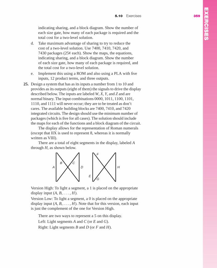
indicating sharing, and a block diagram. Show the number ofeach size gate, how many of each package is required and thetotal cost for a two-level solution.
d. Take maximum advantage of sharing to try to reduce the cost of a two-level solution. Use 7400, 7410, 7420, and 7430 packages (25¢ each). Show the maps, the equations,indicating sharing, and a block diagram. Show the number of each size gate, how many of each package is required, andthe total cost for a two-level solution.
e. Implement this using a ROM and also using a PLA with fiveinputs, 12 product terms, and three outputs.
25. Design a system that has as its inputs a number from 1 to 10 andprovides as its outputs (eight of them) the signals to drive the displaydescribed below. The inputs are labeled W, X, Y, and Z and arenormal binary. The input combinations 0000, 1011, 1100, 1101,1110, and 1111 will never occur; they are to be treated as don’tcares. The available building blocks are 7400, 7410, and 7420integrated circuits. The design should use the minimum number ofpackages (which is five for all cases). The solution should includethe maps for each of the functions and a block diagram of the circuit.
The display allows for the representation of Roman numerals(except that IIX is used to represent 8, whereas it is normallywritten as VIII).
There are a total of eight segments in the display, labeled Athrough H, as shown below.
Version High: To light a segment, a 1 is placed on the appropriatedisplay input (A, B, . . . , H ).
Version Low: To light a segment, a 0 is placed on the appropriatedisplay input (A, B, . . . , H ). Note that for this version, each inputis just the complement of the one for Version High.
There are two ways to represent a 5 on this display.
Left: Light segments A and C (or E and G).
Right: Light segments B and D (or F and H).
ACB
D
E
F
G
H
5.10 Exercises 359
EX
ER
CIS
ES
mar91647_c05c_319_364.qxd 11/14/08 1:50 PM Page 359

This is really four separate problems, one for each version ofthe design.
5.11 CHAPTER 5 TEST (60 MINUTES)1. Implement the following functions using only two of the decoders
described below and two 8-input OR gates.
f(w, x, y, z) � �m(0, 4, 5, 6, 7, 12, 15)
g(w, x, y, z) � �m(1, 3, 12, 13, 14, 15)
360 Chapter 5 Designing Combinational Systems
Left
1 2 3 4 5
6 7 8 9 10
Right
1 2 3 4 5
6 7 8 9 10
The following illustration shows all digits as they should becoded for each of these, with a lit segment represented by a boldline and an unlit segment represented by a dashed line.E
XE
RC
ISE
SC
HA
PT
ER
TE
ST
mar91647_c05c_319_364.qxd 11/14/08 1:50 PM Page 360

5.11 Chapter 5 Test 361
EN1 EN2� a b c 0 1 2 3 4 5 6 7
0 X X X X 0 0 0 0 0 0 0 0X 1 X X X 0 0 0 0 0 0 0 01 0 0 0 0 1 0 0 0 0 0 0 01 0 0 0 1 0 1 0 0 0 0 0 0 1 0 0 1 0 0 0 1 0 0 0 0 01 0 0 0 1 0 0 0 1 0 0 0 01 0 1 0 0 0 0 0 0 1 0 0 01 0 1 0 1 0 0 0 0 0 1 0 01 0 1 1 0 0 0 0 0 0 0 1 01 0 1 0 1 0 0 0 0 0 0 0 1
01
4567
23
abc
EN1EN2�
2. Consider the three functions, the maps of which are shown below:
Implement them on the PLA shown here. Be sure to label theinputs and the outputs. Full credit if you use eight terms or less.
f
00 01 11 10
00
01
11
10
w xy z
11
1
1
1
11
111
g
00 01 11 10
00
01
11
10
w xy z
111
11 1
1
h
00 01 11 10
00
01
11
10
w xy z
11
1
11
1
11
CH
AP
TE
R T
ES
T
mar91647_c05c_319_364.qxd 11/14/08 1:50 PM Page 361

362 Chapter 5 Designing Combinational Systems
3. For the same set of functions, implement them with the ROMshown. Be sure to label the inputs and the outputs.
CH
AP
TE
R T
ES
T
mar91647_c05c_319_364.qxd 11/14/08 1:50 PM Page 362
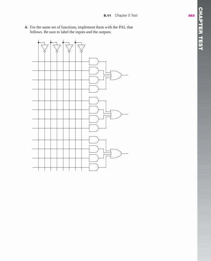
5.11 Chapter 5 Test 363
4. For the same set of functions, implement them with the PAL thatfollows. Be sure to label the inputs and the outputs.
CH
AP
TE
R T
ES
T
mar91647_c05c_319_364.qxd 11/14/08 1:50 PM Page 363

CH
AP
TE
R T
ES
T364 Chapter 5 Designing Combinational Systems
5. For the same set of functions, we have available as componentsthree NAND gates (as many inputs as you need) and some activelow input, active low enable decoders, as shown below (as manyas you need).
EN a b 0 1 2 3
1 X X 1 1 1 10 0 0 0 1 1 10 0 1 1 0 1 1 0 1 0 1 1 0 10 1 1 1 1 1 0
0123
EN �
a
b
Show a diagram of a circuit to implement these functions with onlythese components.
5 points extra credit: Show a diagram that uses only 3 eight-inputNAND gates and 4 of these decoders.
mar91647_c05c_319_364.qxd 11/14/08 1:50 PM Page 364

C H A P T E R
6Analysis ofSequential Systems
Up to now everything has been combinational—that is, the outputat any instant of time depends only on what the inputs are at thattime. (This ignores the small delay between the time the input of
a circuit changes and when the output changes.)We will now focus on systems that have memory, referred to as
sequential systems or as finite state machines. Thus, the output willdepend not only on the present input but also on the past history—whathas happened earlier.
We will deal primarily with clocked systems (sometimes referred toas synchronous). A clock is just a signal that alternates (over time)between 0 and 1 at a regular rate.* Two versions of a clock signal areshown in Figure 6.1. In the first, the clock signal is 0 half of the time and1 half of the time. In the second, it is 1 for a shorter part of the cycle. Thesame clock is normally connected to all flip flops.
The period of the signal (T on the diagram) is the length of onecycle. The frequency is the inverse (1/T). A frequency of 200 MHz (mega-hertz, million cycles per second) corresponds to a period of 5 nsec†
(5 nanoseconds, 5 billionths of a second). The exact values are notimportant in most of the discussion that follows.
365
Figure 6.1 Clock signals.
T
*Although the clock is usually a regular waveform as shown, the regularity of the clock isnot crucial to the operation of most sequential systems.
†1/(200 � 106) � (1000/200) � 10�9 � 5 � 10�9 � 5 nsec.
mar91647_c06a_365_372.qxd 11/14/08 11:22 AM Page 365

In most synchronous systems, change occurs on the transition of theclock signal. We will look at this in more detail as we introduce the sev-eral types of flip flops, clocked binary storage devices.
The block diagram of Figure 6.2 is a conceptual view of a synchro-nous sequential system. A sequential system consists of a set of memorydevices and some combinational logic. This diagram depicts a systemwith n inputs (x’s), in addition to the clock, k outputs (z’s), and m binarystorage devices (q’s). Each memory device may need one or two inputsignals. Many systems have only one input and one output, although wewill see examples with several of each, and some where there is no input,other than the clock. Many memory devices provide the complementedoutput (q�) as well as q.
366 Chapter 6 Analysis of Sequential Systems
Figure 6.2 Conceptual view of a sequential system.
Combinational Logicxn zk
x1
z1
q1
qmMemory
Clock
. . .
. . .
. . .
. . .
The inputs to the combinational logic are the system inputs and thecontents of memory; the combinational logic outputs are the system out-puts and signals to update the memory.
In Section 6.2, we will introduce the simplest storage device, thelatch. It is a static device constructed of gates. The output changesimmediately whenever the input changes; there is no clock involved.Latches are used primarily for temporary (buffer) storage.
In Section 6.3, we will develop the most common binary storagedevice, the flip flop. A flip flop almost always has two outputs, q and q�;that is, both the bit stored and its complement. It may have one or twoinputs (indeed, they used to make one with three); we will describe sev-eral types of flip flops.
In Section 6.1, we will introduce state table, state diagrams, andtiming traces. In Section 6.4, we will discuss the analysis of sequentialsystems.
6.1 STATE TABLES AND DIAGRAMSA simple example of a sequential system is the first of a set of contin-uing examples for sequential systems. (Others will be introduced inChapter 7.)
mar91647_c06a_365_372.qxd 11/14/08 11:22 AM Page 366

CE6. A system with one input x and one output z such that z � 1iff x has been 1 for at least three consecutive clock times.*
For this example, the system must store in its memory informationabout the last three inputs and produce an output based on that. What isstored in memory is the state of the system. Memory consists of a set ofbinary devices. They may just store the last few inputs, but it is oftenmore economical to code the information in a different way. Sometimes,a finite number of recent inputs is not adequate.
A timing trace is a set of values for the input and the output (andsometimes the state or other variables of the system, as well) at consecu-tive clock times. It is often used to clarify the definition of systembehavior or to describe the behavior of a given system. The inputs are anarbitrary set of values that might be applied to the system, chosen so asto demonstrate the behavior of the system. For CE6, the timing trace isshown in Trace 6.1.
6.1 State Tables and Diagrams 367
*In Section 6.3, we will define exactly when during the clock that the input matters.
Trace 6.1 Three consecutive 1’s.
x 0 1 1 0 1 1 1 0 0 1 0 1 1 1 1 1 0 0z ? 0 0 0 0 0 0 1 0 0 0 0 0 0 1 1 1 0 0 0 0
For CE6, the output depends only on the state of the system (not thepresent input) and, thus, occurs after the desired input pattern hasoccurred. Such a system is called a Moore model, named after E. F. Moore. The output for the first input is shown as unknownbecause we have no history of what happened before. (If the systemwere initialized to indicate that no 1’s had yet occurred, then that out-put would be 0.) After three consecutive inputs are 1, the system goesto a state where the output is 1, and remains there as long as the inputremains 1.
Several designs are possible for this system. We will defer untilChapter 7 our discussion of the techniques for designing a system from averbal description. At this point, we will introduce two tools for describingsequential systems.
A state table shows, for each input combination and each state, whatthe output is and what the next state is, that is, what is to be stored inmemory after the next clock.
A state diagram (or state graph) is a graphical representation of thebehavior of the system, showing for each input combination and eachstate what the output is and what the next state is, that is, what is to bestored in memory after the next clock.
Table 6.1 shows an example of a state table, one that does describeCE6, although that is not obvious at this point.
mar91647_c06a_365_372.qxd 11/14/08 11:22 AM Page 367

We will refer to the present state as q and the next state as q★. (Somebooks use Q or q� or q(t � �) to represent the next state.) The next stateis what will be stored in memory after this clock transition. That willthen become the present state at the next clock time. The next state is afunction of the present state and the input, x. The output, in this example,depends on the present state, but not the present input. The output onlychanges when the state changes, at the time of a clock transition. Thefirst row of the table signifies that if the system is in state A, that is, factA is stored in memory and the input is a 0, then the next state is A (thatis, A is to be stored in memory again); and if fact A is stored in memoryand the input is a 1, then the next state is B. Whenever the system is instate A (or B or C), the output is 0.
The state diagram that corresponds to this state table is shown inFigure 6.3. Each state is represented by a circle. Also included in thecircle is the output for that state. Each line coming out of a circle repre-sents a possible transition. The label on the line indicates the input thatcauses that transition. There must be one path from each state for eachpossible input combination. (In this example, there is only one input;thus, there are two paths.) Sometimes, the same next state is reached forboth input combinations and a single line is shown either with two labelsor with a don’t care (X). This state diagram contains the identicalinformation as the state table.
368 Chapter 6 Analysis of Sequential Systems
Figure 6.3 A state diagram.
1
00 0
11B0
C0
0
A0
D1
1
Table 6.1 A state table.
Present Next state Presentstate x � 0 x � 1 output
A A B 0B A C 0C A D 0D A D 1
If we were given the state table or diagram, we can construct thetiming trace. In Trace 6.2, we repeat the previous trace but include thestate.
mar91647_c06a_365_372.qxd 11/14/08 11:22 AM Page 368

Whether we know the initial state or not, the state table and the statediagram both show that a 0 input takes the system to state A from allstates. From state A, a 1 input takes the system to state B; from B, it goesto C; from C, it goes to D; and from D, it remains in D.
In some systems, the output depends not only on the present state ofthe machine, but also on the present input. This type of system is referredto as a Mealy model (after G. B. Mealy). The state table has as many out-put columns as the next state portion (one for each possible input combi-nation). An example (which we will return to in the next chapter) isshown in Table 6.2.
6.1 State Tables and Diagrams 369
Trace 6.2 Trace with state.
x 0 1 1 0 1 1 1 0 0 1 0 1 1 1 1 1 0 0q ? A B C A B C D A A B A B C D D D A A ?z ? 0 0 0 0 0 0 1 0 0 0 0 0 0 1 1 1 0 0 0 0
Figure 6.4 State diagram for the Mealy system of Table 6.2.
0/0
0/0two or more 1’s
one 1
no 1’s
1/1
0/0
1/0
1/0B
A
C
Table 6.2 State table for a Mealy model system.
q★ zq x � 0 x � 1 x � 0 x � 1
A A B 0 0B A C 0 0C A C 0 1
The Mealy model state diagram is different from the Moore model.The output is associated with the transition, rather than the state, asshown in Figure 6.4. Each path has a double label: the input causing thetransition, followed by a slash and the output that occurs when the sys-tem is in that state and that is the input. Thus, from state A, the path tostate B is labeled 1/0, meaning that that path is followed when x � 1, andthe output produced is 0.
mar91647_c06a_365_372.qxd 11/14/08 11:22 AM Page 369
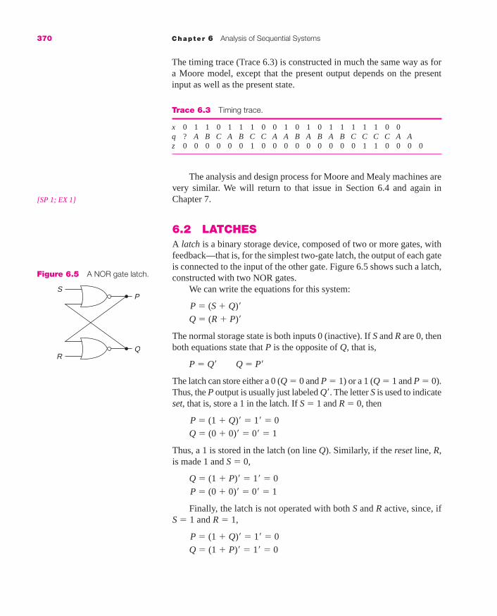
The timing trace (Trace 6.3) is constructed in much the same way as fora Moore model, except that the present output depends on the presentinput as well as the present state.
[SP 1; EX 1]
370 Chapter 6 Analysis of Sequential Systems
Trace 6.3 Timing trace.
x 0 1 1 0 1 1 1 0 0 1 0 1 0 1 1 1 1 1 0 0q ? A B C A B C C A A B A B A B C C C C A Az 0 0 0 0 0 0 1 0 0 0 0 0 0 0 0 0 1 1 0 0 0 0
The analysis and design process for Moore and Mealy machines arevery similar. We will return to that issue in Section 6.4 and again inChapter 7.
6.2 LATCHESA latch is a binary storage device, composed of two or more gates, withfeedback—that is, for the simplest two-gate latch, the output of each gateis connected to the input of the other gate. Figure 6.5 shows such a latch,constructed with two NOR gates.
We can write the equations for this system:
P � (S � Q)�
Q � (R � P)�
The normal storage state is both inputs 0 (inactive). If S and R are 0, thenboth equations state that P is the opposite of Q, that is,
P � Q� Q � P�
The latch can store either a 0 (Q � 0 and P � 1) or a 1 (Q � 1 and P � 0).Thus, the P output is usually just labeled Q�. The letter S is used to indicateset, that is, store a 1 in the latch. If S � 1 and R � 0, then
P � (1 � Q)� � 1� � 0
Q � (0 � 0)� � 0� � 1
Thus, a 1 is stored in the latch (on line Q). Similarly, if the reset line, R,is made 1 and S � 0,
Q � (1 � P)� � 1� � 0
P � (0 � 0)� � 0� � 1
Finally, the latch is not operated with both S and R active, since, ifS � 1 and R � 1,
P � (1 � Q)� � 1� � 0
Q � (1 � P)� � 1� � 0
Figure 6.5 A NOR gate latch.
PS
RQ
mar91647_c06a_365_372.qxd 11/26/08 12:11 PM Page 370

Both outputs would be 0 (not the complement of each other). Further, ifboth S and R became inactive (went to 0) simultaneously, it is not clearto which state the latch would go (since either Q � 0 or Q � 1 wouldsatisfy the logic equations). What happens would depend on such issuesas whether they go to 0 at exactly the same time or one input goes to 0ahead of the other, in which case the last 1 will dominate. Otherwise,such factors that are beyond the normal interest of the logic designer(such as the stray capacitance or the gain of the individual transistors)will determine the final state. To avoid this problem, we ensure that bothinputs are not active simultaneously.
More complex latches can also be built. We will look at a gated latch,as shown in Figure 6.6. When the Gate signal is inactive (� 0), SG and RGare both 0, and the latch remains unchanged. Only when Gate goes to 1, cana 0 or 1 be stored in the latch, exactly as in the simpler latch of Figure 6.5.
[SP 2; EX 2]
6.3 Flip Flops 371
Figure 6.6 A gated latch.
S SG
RG
Gate
R
Q
Q�
*Many flip flops also have asynchronous clear and/or preset inputs that override the clockand put a 0 (clear) or a 1 (preset) in the flip flop immediately, in much the same way as inthe simple SR latch. We will address that issue shortly.
6.3 FLIP FLOPSA flip flop is a clocked binary storage device, that is, a device that storeseither a 0 or a 1. Under normal operation, that value will only change onthe appropriate transition of the clock.* The state of the system (that is,what is in memory) changes on the transition of the clock. For some flipflops, that change takes place when the clock goes from 1 to 0; that isreferred to as trailing-edge triggered. For others, that change takes placewhen the clock goes from 0 to 1; that is referred to as leading-edgetriggered. What is stored after the transition depends on the flip flop datainputs and what was stored in the flip flop prior to the transition.
Flip flops have one or two outputs. One output is the state of theflip flop. If there are two, the other output is the complement of the state.
mar91647_c06a_365_372.qxd 11/14/08 11:22 AM Page 371

Individual flip flops almost always have both outputs. However, whenseveral flip flops are contained in one integrated circuit package, pinlimitations may make only the uncomplemented output available.
A simple SR master/slave flip flop can be constructed with twogated latches, as shown in Figure 6.7. When the clock is 1, the S and Rinputs establish the values for the first flip flop, the master. During thattime, the slave is not enabled. As soon as the clock goes to 0, the masteris disabled and the slave enabled. The values of the master’s outputs, Xand X�, are determined by the value of S and R just before the trailingedge. These are the inputs of the slave. Thus, the slave (and the flip flopoutput) changes as the clock goes to 0 (on the trailing edge) and remainsthat way until the next clock cycle. We could get a leading-edge triggeredflip flop by connecting the clock to the slave and its complement to themaster. The change in the output of the flip flop is delayed from the edgeof the clock (a somewhat longer delay than that through a gate). Com-mercial flip flops use a more complex but faster circuit.
We will concentrate on two types of flip flops, the D and the JK. TheD flip flop is the most straightforward and is commonly found in pro-grammable logic devices (Chapter 8). The JK flip flop almost alwaysproduces the simplest combinational logic. We will also introduce the SRand T flip flops, in between the discussion of the D and JK, since theynaturally lead to the JK.
372 Chapter 6 Analysis of Sequential Systems
Figure 6.7 A master/slave flip flop.S
R
Clock
Master Slave
X�
X Q�
Q
The simplest flip flop is the D flip flop. The name comes from Delay,since the output is just the input delayed until the next active clock transi-tion. The next state of the D flip flop is the value of D before the clocktransition. Block diagrams of D flip flops, both trailing-edge triggered andleading-edge triggered, are shown in Figure 6.8. The triangle is used
mar91647_c06a_365_372.qxd 11/14/08 11:22 AM Page 372

6.3 Flip Flops 373
Figure 6.8 D flip flop diagrams.
D
q
q�
ClockTrailing-edgetriggered
Leading-edgetriggered
D
q
q�
Clock
We will use two forms of a truth table (Table 6.3) and a state dia-gram to describe the behavior of each type of flip flop. Although theseare particularly simple for the D flip flop, we will show them here aswell. In the first form of the truth table, the flip flop input(s) and thepresent state are in the input columns; in the second, only the flipflop input(s) are needed. The state diagram for a D flip flop is shown inFigure 6.9. It has two states (for all types of flip flops). The transitionpaths are labeled with the input that causes that transition. The output isnot shown in the circle since it is the same as the state.
to indicate which input is the clock. A circle is usually shown on theclock input of a trailing-edge triggered flip flop. (We will do that consis-tently.) Caution is in order, however, since some publications do not dif-ferentiate in the diagram.
Table 6.3 The D flip flop behavioral tables.
D q q� D q�
0 0 0 0 00 1 0 1 11 0 11 1 1
Figure 6.9 D flip flop statediagram.
0 1
1
D
0
0 1
The next state of a flip flop can be described algebraically as a func-tion of its inputs and present state (by obtaining an equation directlyfrom the first truth table). In the case of the D flip flop, the equation is
q� � D
The behavior of a trailing-edge triggered D flip flop is illustrated inthe timing diagram of Figure 6.10a. Unless we know the initial value ofq, that is, what was stored in the flip flop before we started to look, thenq is unknown until after the first negative-going clock transition. That isindicated by the slashed section on the timing diagram. When the firsttrailing edge of the clock occurs, the state of the flip flop is established.
mar91647_c06b_373_390.qxd 11/14/08 11:37 AM Page 373

374 Chapter 6 Analysis of Sequential Systems
Figure 6.10 D flip flop timing diagram.
Clock
D
(a)
q
q�
Clock
D
(b)
Since D is 0 at that time, q goes to 0 (and, of course, q� goes to 1). Notethat there is a slight delay in the output. The input, D, usually changesshortly after the transition, as shown for the first change, but may changeat any time, as long as it has reached the correct value well before thenext active transition. (Note that the second and third changes in D comelater in the clock cycle.) As shown, the q� output is (as the name implies)the opposite of the q output. At the second trailing edge, D is 1; thus, q is1 for the next clock period. At the third trailing edge, D is still 1, and qremains 1 for another clock period. Note that if the D input were to goback and forth between clock transitions, as shown in Figure 6.10b, theoutput would not be affected, since the value of D is only relevant nearthe time of a trailing edge. It would be the same as in Figure 6.10a.*
Next, we will look at the behavior of a leading-edge triggered ver-sion of that flip flop. The tables describing the flip flop need not be mod-ified; the only difference is when the output changes relative to the clock.A timing diagram for a leading-edge triggered D flip flop, using the sameinput as before, is shown in Figure 6.11. The output (the state of the flip
*In some flip flops, the input must be established by the preceding leading edge. We willnot discuss those further.
mar91647_c06b_373_390.qxd 11/14/08 11:37 AM Page 374

6.3 Flip Flops 375
Figure 6.11 Leading-edge triggered D flip flop.
Clock
D
q
Since the behavior of the flip flop at a clock transition depends onthe value of the flip flop inputs prior to that transition, we can connect theoutput of one flip flop to the input of another, as shown in Figure 6.12(with trailing-edge triggered flip flops), and clock them simultaneously.At a clock transition when flip flop q changes, the old value of q isused to compute the behavior of r, as indicated in the timing diagram ofFigure 6.13. The input to the first flip flop has not changed from the lastexample, and thus, q is the same as it was before. (We have not shown q�on this diagram.) At the first trailing edge, the input to r (the output of theq flip flop) is unknown; thus, the output remains unknown after thatclock. At the second trailing edge, the input to r is 0 and thus r goes to 0.That flip flop q changes from 0 to 1 as a result of this clock edge is notrelevant; it is the value of the input before the clock edge that determinesthe behavior of r. The new value of q will be used to determine the
Figure 6.12 Two flip flops.
Dx
q
q�
Clock
D
r
r �
Figure 6.13 Timing for two flip flops.
Clock
D
q
r
flop) changes shortly after the clock goes from 0 to 1 (based on the inputjust before that transition).
mar91647_c06b_373_390.qxd 11/14/08 11:37 AM Page 375

376 Chapter 6 Analysis of Sequential Systems
*Preset is sometimes referred to as set, in which case, clear may be referred to as reset.
behavior of r at the next clock transition. The output of flip flop r is areplica of that of q, delayed by one clock period.
This type of behavior is common throughout sequential systems.Usually, all flip flops in the system are triggered by the same clock.Often, the inputs to flip flops are a function of the contents of the flipflops of the system, as was shown in the global view of a sequential sys-tem at the beginning of this chapter.
Before going on to look at other types of flip flops, we will examinethe behavior of flip flops with static (asynchronous) clear* and presetinputs. Any type of flip flop may have one or both of these available. A Dflip flop with active low (the most common arrangement) clear and pre-set inputs is shown in Figure 6.14. The version on the left uses overbarsfor the complement (the most common notation in the integrated circuitliterature); we will continue to use primes, as on the right, where thebehavior of the flip flop is described by the truth table of Table 6.4. Theclear and preset inputs act immediately (except for circuit delay) andoverride the clock, that is, they force the output to 0 and 1, respectively.Only when both of these static inputs are 1, does the flip flop behave asbefore, with the clock transition and the D input determining the behav-ior. A timing example is shown in Figure 6.15. The clear input becomesactive near the beginning of the time shown, forcing q to 0. As long asthat input remains 0, the clock and D are ignored; thus, nothing changesat the first trailing edge of the clock that is shown. Once the clear returnsto 1, then the clock and D take over; but they have no effect until the nexttrailing edge of the clock. The D input determines the behavior of the flipflop at the next four trailing edges. When the preset input goes to 0, theflip flop output goes to 1. When the preset input goes back to 1, the clockand D once again take over.
Figure 6.14 Flip flop with clear and preset inputs.
D q
CLRClock q�
PRED q
CLR�Clock q�
PRE�
Table 6.4 D flip flop with clear and preset inputsbehavioral table.
PRE� CLR� D q q�
0 1 X X 1 static1 0 X X 0 immediate0 0 X X — not allowed
1 1 0 0 01 1 0 1 0 clocked1 1 1 0 1 (as before)1 1 1 1 1
mar91647_c06b_373_390.qxd 11/14/08 11:37 AM Page 376

Table 6.5 SR flip flop behavioral tables.
S R q q� S R q�
0 0 0 0 0 0 q0 0 1 1 0 1 00 1 0 0 1 0 10 1 1 0 1 1 — not allowed1 0 0 11 0 1 11 1 0 — not1 1 1 — allowed
6.3 Flip Flops 377
Next, we will look at the SR (Set-Reset) flip flop. It has two inputs,S and R, which have the same meaning as those for the SR latch. Itsbehavior is described by the truth tables of Table 6.5 and state diagram ofFigure 6.16. The Set (S) input causes a 1 to be stored in the flip flop at thenext active clock edge; the Reset (R) input causes a 0 to be stored. The Sand R inputs are never made 1 at the same time. Although that would notdamage the flip flop, as in the case of the latch, it is not certain what hap-pens when S and R both go back to 0. Note that in the diagram, each labelis two digits; the first is the value of S and the second the value of R. Two labels are on the path from 0 to 0 since either 00 or 01 will cause theflip flop to return to state 0. (There are also two input combinations thatcause the flip flop to go from state 1 to 1.)
In Map 6.1, we map q� (from the first truth table). Notice that two ofthe squares are don’t cares, since we will never make both S and R equalto 1 at the same time. This allows us to write an equation for the next
Figure 6.15 Timing for flip flop with clear and preset.
Clock
D
q
CLR�
PRE�
Figure 6.16 SR flip flop statediagram.
0001
0010
10
S R
01
0 1
Map 6.1 SR flip flop behavioralmap.
00 01 11 10
0
1
S R
q
q★
X1 1
X 1
mar91647_c06b_373_390.qxd 11/14/08 11:37 AM Page 377

The third type of flip flop is the T (Toggle) flip flop. It has one input,T, such that if T � 1, the flip flop changes state (that is, is toggled), andif T � 0, the state remains the same. The truth tables describing thebehavior of the T flip flop are given in Table 6.6 and the state diagram isshown in Figure 6.18.
378 Chapter 6 Analysis of Sequential Systems
state of the flip flop, q�, in terms of the present state, q, and the inputs,S and R:
q� � S � R�q
The equation says that after the clock, there will be a 1 in the flip flop ifwe set it (S � 1) or if there was already a 1 and we don’t reset it (R � 0).A timing example (where there is only a clear input, not a preset one) isgiven in Figure 6.17. Note that we never made both S and R equal to 1 atthe same time. Also, when both S and R are 0, q does not change.
Figure 6.17 SR flip flop timing diagram.
Clock
CLR�
S
R
q
Figure 6.18 T flip flop statediagram.
0 0
1
T
1
0 1
Table 6.6 T flip flop behavioral tables.
T q q� T q�
0 0 0 0 q0 1 1 1 q�1 0 11 1 0
*The T flip flop must have static clear or preset, since the next state always depends on the previous one. For each of the other types of flip flops, there is at least one inputcombination that will force the flip flop to state 0.
The behavioral equation is
q� � T � q
and a timing example is shown in Figure 6.19.*
mar91647_c06b_373_390.qxd 11/14/08 11:37 AM Page 378

6.3 Flip Flops 379
Figure 6.19 T flip flop timing diagram.
Clock
CLR�
T
q
The last type of flip flop we will present is the JK (where the lettersare not an acronym), which is a combination of the SR and T, in that itbehaves like an SR flip flop, except that J � K � 1 causes the flip flop tochange states (as in T � 1). The truth tables are given in Table 6.7 and thestate diagram is shown in Figure 6.20.
Figure 6.20 JK flip flop state diagram.
0001
0010
1011
J K
0111
0 1
Map 6.2 JK flip flop behavioralmap.
00 01 11 10
0
1
J K
q
q★
1 1
11
Table 6.7 JK flip flop behavioral tables.
J K q q� J K q�
0 0 0 0 0 0 q0 0 1 1 0 1 00 1 0 0 1 0 10 1 1 0 1 1 q�1 0 0 11 0 1 11 1 0 11 1 1 0
From the first truth table, we can derive Map 6.2 and the equation for q�:
q� � Jq� � K�q
A timing example for the JK flip flop is shown in Figure 6.21. Notethat there are times when both J and K are 1 simultaneously; the flip flopjust changes state at those times.
We now have the behavioral aspects of all of the flip flops and canbegin to analyze more complex systems. Before we continue with that,we will look at some of the commercially available flip flop packages. Dand JK flip flops are the most common. We will look at four packages, allof which are available in LogicWorks and in the Breadboard simulator(although the latter two are listed under registers in the simulator).
mar91647_c06b_373_390.qxd 11/14/08 11:37 AM Page 379

380 Chapter 6 Analysis of Sequential Systems
[SP 3, 4; EX 3, 4, 5, 6; LAB]
Figure 6.21 Timing diagram for JK flip flop.
Clock
CLR�
J
K
q
The 7473 is a dual JK flip flop package. It contains two independentJK flip flops, each of which has an active low clear input, and both q andq� outputs. It is trailing-edge triggered (with separate clock inputs foreach of the flip flops). (Each flip flop has four inputs—J, K, clear, andclock—and two outputs—q and q�; it fits in a 14-pin integrated circuitpackage.)
The 7474 is a dual D flip flop, also in a 14-pin package. Since thereis only one data input per flip flop, there are two available pins; they areused for active low preset inputs. It is leading-edge triggered (with sepa-rate clock inputs for each of the flip flops).
There are packages of D flip flops with four or six flip flops. The74174 is a hex (six) D flip flop package, with only a q output for each flipflop and a common leading-edge triggered clock. There is a commonactive low clear (sometimes referred to as a Master Reset). This is a 16-pin package.
Lastly, we have the 74175, a quad (four) D flip flop package. Eachflip flop has both a q and q� output. There is a common leading-edge trig-gered clock and a common active low clear. Once again, this is a 16-pinpackage. The pin connections for these are shown in Appendix A.6.
6.4 ANALYSIS OF SEQUENTIAL SYSTEMS
In this section, we will examine some small state machines (consisting offlip flops and gates) and analyze their behavior, that is, produce timingdiagrams, timing traces, state tables, and state diagrams. We will alsolook at the relationship between the state table and the timing.
The first example, the circuit of Figure 6.22, is a circuit with twotrailing-edge triggered D flip flops. (We will call the flip flops q1 and q2;sometimes we will use names, such as A and B.)
mar91647_c06b_373_390.qxd 11/14/08 11:37 AM Page 380

6.4 Analysis of Sequential Systems 381
Figure 6.22 A D flip flop Moore model circuit.x
z
D q2
q1� q 2�
D q1
Clock
From the circuit, we find
D1 � q1 q2� � x q1�
D2 � x q1
z � q2�
We will first construct the state table. Since this is a Moore model,there is only one output column. The next state part is particularly easyfor a D flip flop q� � D. We first complete the output (z) column and theq1
� (� D1) part of the table as shown in Table 6.8a.Finally, we add q2
�(D2) to produce the complete state table ofTable 6.8b.
Table 6.8a Partial state table.
q1� q2
�
q1q2 x � 0 x � 1 z
0 0 0 1 10 1 0 1 01 0 1 1 11 1 0 0 0
Table 6.8b Complete state table.
q1� q2
�
q1q2 x � 0 x � 1 z
0 0 0 0 1 0 10 1 0 0 1 0 01 0 1 0 1 1 11 1 0 0 0 1 0
Figure 6.23 A Moore statediagram.
0
0
00
001
010
101
110
1
11
1
Figure 6.24 A Moore model circuit.
J
K B�
BJ
K A�
A
Clock
x
z
The corresponding state diagram is shown in Figure 6.23.We will now look at a Moore model circuit with JK flip flops (See
Figure 6.24).
mar91647_c06b_373_390.qxd 11/26/08 12:16 PM Page 381

This is a Moore model, since the output z, which equals A � B, is a func-tion of the state (that is, the contents of the flip flops) and not of theinput x.
We will now write equations for the flip flop inputs and the output,and, from them, construct a state table:
JA � x KA � xB�
JB � KB � x � A�
z � A � B
The output column comes directly from the z equation. We can now fillin the next state section one entry at a time. For the first entry, since x �A � B � 0, JA � KA � 0 and JB � KB � 1. From the flip flop behavioraltable of Table 6.7 (Section 6.3), we can see that A does not change state,but B does. Thus, the next state is 0 1. Next, for x � A � 0 and B � 1(the second row of the first column), JA � KA � 0 and JB � KB � 1.Again, A does not change state, but once again B does. The resulting nextstate is 00. At this point, we have the state table of Table 6.9a.
382 Chapter 6 Analysis of Sequential Systems
Table 6.9a State table with firsttwo entries.
A� B�
A B x � 0 x � 1 z
0 0 0 1 00 1 0 0 11 0 11 1 1
Table 6.9b State table with A�
entered.
A� B�
A B x � 0 x � 1 z
0 0 0 1 00 1 0 1 11 0 1 0 11 1 1 1 1
We can continue through the remaining entries, or we can look atthe equations for one flip flop at a time (as we did with the D flip flops).When x � 0 (no matter what A and B are), JA � KA � 0 and flip flop Adoes not change state. Thus, we can complete A� for x � 0, as inTable 6.9b. When x � 1, JA � 1 and KA � B�. For the two rows whereB � 0 (the first and third), JA and KA are both 1 and A toggles. For thetwo rows where B � 1 (the second and fourth), JA � 1 and KA � 0,putting a 1 in flip flop A. That results in the partial table (where A� hasbeen filled in) of Table 6.9b.
mar91647_c06b_373_390.qxd 11/14/08 11:37 AM Page 382

Now we can complete the B� section of the table. When A � 0 (the firsttwo rows of both columns), JB � KB � 1 and B changes state. WhenA � 1, JB � KB � x. For x � 0 (the first column, last two rows), Bremains unchanged. Finally, for A � 1 and x � 1, JB � KB � 1 and Bchanges, producing the completed Table 6.9c.
6.4 Analysis of Sequential Systems 383
Another technique to construct the state table is to use the equationswe developed in the last section for the next state, namely,
q� � Jq� � K�q
Using the values from this problem, we obtain
A� � JAA� � K�AA � xA� � (xB�)�A � xA� � x�A � AB
B� � JBB� � K�BB � (x � A�)B� � (x � A�)�B
� xB� � A�B� � x�AB
We can now construct the state table as we did with D flip flops. Theseequations give exactly the same results as before.
For this example, we will produce a timing trace and a timing dia-gram if we are given the input x and the initial state.* The values of x andthe initial values of A and B in Trace 6.4 are given.
Table 6.9c Completed state table.
A� B�
A B x � 0 x � 1 z
0 0 0 1 1 1 00 1 0 0 1 0 11 0 1 0 0 1 11 1 1 1 1 0 1
Trace 6.4 Trace for Table 6.9.
x 0 0 1 0 1 1 0A 0 0 0 1 1 1 0 0B 0 1 0 1 1 0 1 0 1
z 0 1 0 1 1 1 1 0 1
→
→
*The process is really a repetition of what we did in Trace 6.2. The major differences are that there we had state names and here we have the values of the state variables (flipflops).
mar91647_c06b_373_390.qxd 11/14/08 11:37 AM Page 383

At the first clock edge, the values in the shaded box determine the nextstate (the box to the right) and the present output (the box below). Thenext state is obtained from the first row (AB � 00) and the first column(x � 0), the shaded square in Table 6.9c. The output is just the value of zin the first row. (Only the state is needed to determine the output.) For thenext column of the timing trace, we start the process over again; this iseffectively a new problem. The state is 01 (second row of the state table)and the input is 0, giving a next state of 00. This continues through suc-cessive inputs. The last input shown, a 0 when the system is in state 01takes the system to state 00. We know that state and that output, eventhough we do not know the input any longer. Finally, for this example,we can determine the output and the value of B for one more clock time,since, from state 00, the next state is either 01 or 11, both of which haveB � 1 and a 1 output. (We cannot go any further.)
In Figure 6.25, we will next look at a timing diagram for the samesystem with the same input sequence. We must look at the value of thevariables (A, B, and x) just before the trailing edge. From that, we knowthe present state and the input, and can determine what the values for Aand B must be during the next clock period. At any time that we know Aand B, we can determine z.
384 Chapter 6 Analysis of Sequential Systems
Figure 6.25 Timing diagram for Table 6.9.
Clock
x
A
B
z
We did not need to construct the state table to obtain either the tim-ing diagram or the trace. We could, at each clock trailing edge, determinethe behavior of each flip flop. The output can then be constructed last,since it is just the OR of the two state variables (A and B). Thus, when thefirst clock edge arrives, A � B � x � 0 and, thus, JA � KA � 0, leavingA at 0. At the same time, JB � KB � 1 and thus B toggles, that is, goes to1. We can now shift our attention to the next clock time and repeat thecomputations.
At this point, a word is in order about the initial value. For thisexample, we assumed that we knew what was stored in A and B when the
mar91647_c06b_373_390.qxd 11/14/08 11:37 AM Page 384

first clock arrived. That may have been achieved using a static clearinput, which was not shown to simplify this problem. In some cases, wecan determine the behavior of the system after one or two clock periodseven if we did not know the initial value. (That will be the case in thenext example.) But, in this problem, we must initialize the system. (Trythe other initial states and note that each follows a completely differentsequence over the time period shown.) Finally, for this problem (a Mooremodel), the state diagram is given in Figure 6.26.
Figure 6.26 State diagram forTable 6.9.
0
0
1
11
1
0 00
0 11
1 11
1 01
0
0
In some systems, the output depends on the present input, as well asthe state. From a circuit point of view, that just means that z is a functionof x, as well as the state variables. This type of circuit is referred to as aMealy model. An example of such a system is shown in Figure 6.27.
6.4 Analysis of Sequential Systems 385
Figure 6.27 A Mealy model.
q2
q2�
Dq1
q1�
D
xz
Clock
mar91647_c06b_373_390.qxd 11/14/08 11:37 AM Page 385

Note that state 11 is never reached; this problem really only has 3 states(although when the system is first turned on, it could start in state 11).But after the first clock, it will leave that state and never return. Thatbecomes obvious from the state diagram of Figure 6.28.
386 Chapter 6 Analysis of Sequential Systems
The flip flop input and the output equations are
D1 � xq1 � xq2
D2 � xq�1q�2z � xq1
Of course, with D flip flops, q� � D. Thus,
q1� � xq1 � xq2
q2� � xq�1q�2
From that, we obtain the state table of Table 6.10. Notice that we needtwo output columns, one for x � 0 and one for x � 1.
Table 6.10 State table for the Mealy system.
q� zq x � 0 x � 1 x � 0 x � 1
0 0 0 0 0 1 0 00 1 0 0 1 0 0 01 0 0 0 1 0 0 11 1 0 0 1 0 0 1
Figure 6.28 State diagram fora Mealy model.
0/0
0/0
0/0 1/1
1/1
0/0
1/0
1/00 1
0 0 1 1
1 0
Notice that there is no path into state 11. Also note that whenever there isa 0 input, we return to state 00. Thus, even if we do not initialize this sys-tem, it will behave properly after the first 0 input.
We will next look at the timing trace (see Trace 6.5, where the inputis given and shown in tan) and then at the timing diagram for this system.
mar91647_c06b_373_390.qxd 11/14/08 11:37 AM Page 386

6.4 Analysis of Sequential Systems 387
Even though we do not know the initial state (the ? for q1 and q2), the 0input forces the system to state 00 at the next clock time and we can com-plete the trace. Note that the output is known for two clock periods afterthe input is not, since the system cannot reach state 10 (the only state forwhich there is a 1 output) any sooner than that. A word of caution: Thepresent state and the present input determine the present output and thenext state, as indicated.
The timing diagram for this example is shown in Figure 6.29. Itillustrates a peculiarity of Mealy systems.* Note that there is a false out-put (sometimes referred to as a glitch), that is, the output goes to 1 for ashort period even though that is not indicated in the timing trace nor inthe state table.
The output comes from combinational logic; it is just xq1. If the input xdoes not change simultaneously with the trailing edge of the clock (as isthe case here), and it remains 1 after q1 goes to 1, the output will go to 1.But the output indicated by the state table or the timing trace is basedon the value of q1 at the time of the next clock. The false output is notusually important, since the output of a Mealy system is mainly of inter-est at clock times (that is, just before the edge on which flip flops mightchange state). Furthermore, it is often the case that system inputs change
Trace 6.5 Mealy model timing.
x 0 1 1 0 1 1 1 1 0q1 ? 0 0 1 0 0 1 1 1 0q2 ? 0 1 0 0 1 0 0 0 0
z 0 0 0 0 0 0 1 1 0 0 0
→
→
Figure 6.29 Illustration of false output.
Clock
x
q1
q2
z
false output
*In the timing diagram, the delay through the output AND gate is ignored since it istypically shorter than that of the flip flop.
mar91647_c06b_373_390.qxd 11/14/08 11:37 AM Page 387

388 Chapter 6 Analysis of Sequential Systems
simultaneously with the trailing edge of the clock.* The glitch occurredonly because x changed well after the flip flop change. As the change inx gets closer (in time) to the changes in q (that is, the clock edge), theglitch gets narrower and if x goes to 0 at the same time that q1 goes to 1,the false output disappears.
Consider the following circuit with one JK and one D flip flop:EXAMPLE 6.1a
q2
q2�
Dq1
q1�
J
K
x
z
Clock
The output, z � q1q2, does not depend on the input x; thus, this is a Mooremodel. (This system also produces an output of 1 if the input is 1 for threeor more consecutive clock periods [CE 6]).
The input equations for the system are
J1 � xq2 K1 � x�
D2 � x(q1 � q�2)
Notice that when x � 0, J1 is 0, K1 is 1, and D2 is 0; thus the system goesto state 00. When x � 1,
J1 � q2 K1 � 0 D2 � q1 � q�2
Flip flop q1 goes to 1 when q2 � 1 and is unchanged otherwise. (Of course,q1 remains at 1 in state 10.) Flip flop q2 goes to 1 when q1 � 1 or q2 � 0 andto 0 only if q1 � 0 and q2 � 1.
We could also use, for q1, the equation
q� � Jq� � K�q
and obtain
q1� � xq2q�1 � xq1 � x(q2 � q1)
From either approach, we get the following state table:
*Sometimes, circuitry is added to synchronize the input changes with the clock edge.
q1★ q2
★
q1 q2 x � 0 x � 1 z
0 0 0 0 0 1 00 1 0 0 1 0 01 0 0 0 1 1 01 1 0 0 1 1 1
mar91647_c06b_373_390.qxd 11/14/08 12:03 PM Page 388

6.4 Analysis of Sequential Systems 389
There is never a false output in a Moore model, since the output dependsonly on the state of the flip flops, and they all change simultaneously, on thetrailing edge of the clock. The output is valid for a whole clock period, fromjust after one negative-going transition to just after the next.
If the AND gate of Example 6.1a had a third input, x�, then z � x�q1q2 andthis would be a Mealy model. The next state portion of the state table andof the timing diagram would be unchanged. There would be two columns inthe state table.
Clock
x
z
q1
q2
EXAMPLE 6.2
R
D q4
q3�q2� q 4�
S q3x
T q2
Clock
q1�K
J q1
This is the same state table as in Table 6.1 if we note that A has been codedas 00, B as 01, C as 10, and D as 11.
This system produces the following timing diagram:
EXAMPLE 6.1b
q1★ q2
★ zq1 q2 x � 0 x � 1 x � 0 x � 1
0 0 0 0 0 1 0 00 1 0 0 1 0 0 01 0 0 0 1 1 0 01 1 0 0 1 1 1 0
The z in the timing diagram would remain 0 until after x goes to 0 (one clocktime later than in Example 6.1a).
mar91647_c06b_373_390.qxd 11/14/08 11:38 AM Page 389

390 Chapter 6 Analysis of Sequential Systems
[SP 5, 6, 7, 8; EX 7, 8, 9; LAB]
Complete the timing trace as far as possible. Assume that the system isinitially in state 0000. The given values are shown in brown.
J1 � K1 � xq4
T2 � q1�
S2 � q2� R2 � q2
D4 � q3
Therefore,
q1 changes state only when xq4 � 1
q2 changes state only when q1 � 0
q3� � q2�
q4� � q3
x 1 1 1 0 1 1
q1 0 0 0 1 1 0 0 0 0
q2 0 1 0 1 1 1 0 1 1 0
q3 0 1 0 1 0 0 0 1 0 0 1
q4 0 0 1 0 1 0 0 0 1 0 0 1
After the first clock, q1 remains at 0, q2 toggles, q3 is loaded with 1 (q2�),and q4 goes to 0 (from q3). After the last input is known for this circuit, wecan determine the next value of q1 as long as the present value of q4 is 0(since xq4 will be 0). The next state of each of the other flip flops dependsonly on the present state of the one to its left. Thus, we can find a value forq2 one clock time after q1 is known, for q3 one clock time after that, and forq4 one additional clock time later.
6.5 SOLVED PROBLEMS
1. For each of the following state tables, show a state diagram andcomplete the timing trace as far as possible (even after the inputis no longer known).
a. q1★ q2
★ zq1q2 x � 0 x � 1 x � 0 x � 1
0 0 0 0 1 0 0 10 1 0 0 0 0 0 01 0 1 1 0 1 1 11 1 1 0 1 0 1 0
mar91647_c06b_373_390.qxd 11/14/08 11:38 AM Page 390
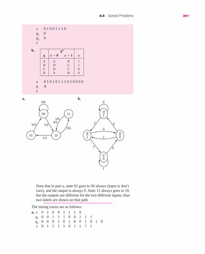
6.5 Solved Problems 391
q★
q x � 0 x � 1 z
A A B 1B D C 1C D C 0D A B 0
x 0 1 0 0 1 1 1 0q1 0q2 0z
b.
x 0 1 0 1 0 1 1 1 0 1 0 0 0 0q Az
a. b.0/0
1/1
X/0 1/1
01
00
10
0/1
1/00/1
11A1
C0
0
0
0
1
1
1
0
B1
D0
1
Note that in part a, state 01 goes to 00 always (input is don’tcare), and the output is always 0. State 11 always goes to 10,but the outputs are different for the two different inputs; thustwo labels are shown on that path.
The timing traces are as follows:
a. x 0 1 0 0 1 1 1 0q1 0 0 1 1 1 0 0 1 1 1q2 0 0 0 1 0 1 0 0 1 0 1 0z 0 1 1 1 1 0 1 1 ? 1
mar91647_c06c_391_398.qxd 11/14/08 11:11 AM Page 391

392 Chapter 6 Analysis of Sequential Systems
Since state 11 always goes to state 10 (independent of theinput), we can determine the next state for the second clockafter the input is no longer known. At the first clock after thelast input, the output is unknown, but at the next one, we knowthat it must be 1, since the output is 1 from state 10, no matterwhat the input is. Note that we can determine q2 for twoadditional clock times.
b. x 0 1 0 1 0 1 1 1 0 1 0 0 0 0q A A B D B D B C C D B D A A Az 1 1 1 0 1 0 1 0 0 0 1 0 1 1 1 1
Since state A goes to either A or B, and the output in each ofthose states is 1, we can determine the output for one extraclock time.
2. Analyze the following latch; give the appropriate inputs andoutputs meaningful labels.
PA
BQ
P � (AQ)� Q � (BP)�
If A � B � 0,
P � Q � 1
If A � B � 1,
P � Q� Q � P�
If A � 0 and B � 1,
P � 1 Q � 0
If A � 1 and B � 0,
Q � 1 P � 0
This is an active low input latch, where both inputs active(A � B � 0) is not allowed. The store state is A � B � 1(inactive), where the outputs are the complement of each other.When A is active, P is made 1 (and Q � 0). When B is active,Q � 1 and P � 0. Thus, we could label the latch as follows:
mar91647_c06c_391_398.qxd 11/14/08 11:11 AM Page 392

6.5 Solved Problems 393
S
R
CLR�
Q�
Q
Clock
J
K
Clock
CLR�
PRE�
q�
q
Q�R�
S�Q
3. Consider the trailing-edge triggered flip flops shown.
a. b. c.
D
Q�
Q
Clock
a. Show a timing diagram for Q.
Clock
S
R
CLR�
Clock
D
b. Show a timing diagram for Q if
i. there is no CLR� input.
ii. the CLR� input is as shown.
c. Show a timing diagram for Q if
i. there is no PRE� input.
ii. the PRE� input is as shown (in addition to the CLR� input).
mar91647_c06c_391_398.qxd 11/14/08 11:11 AM Page 393

394 Chapter 6 Analysis of Sequential Systems
Clock
J
K
CLR�
PRE �
a.
Clock
D
Q
The state of the flip flop is not known until the first trailingedge. At that point, D determines what is to be stored. Thus,the first time, Q goes to 1; the second time, Q goes to 0; thethird time, Q goes to (stays at) 0. When D changes betweenclock times, that does not affect the behavior; it is the valuejust before the trailing edge that matters.
Clock
S
R
Q
Q
CLR �
i.
ii.
b.
mar91647_c06c_391_398.qxd 11/14/08 11:11 AM Page 394

6.5 Solved Problems 395
Without the clear, we do not know what Q is until after thefirst trailing edge. At that point, since S � 1, Q goes to 1. Atthe next clock, both S and R are 0; thus, Q does not change.Since R � 1 for the next two clock times, Q goes to 0. ThenS � 1, making Q � 1; both are 0 leaving Q at 1; and finallyR � 1, returning Q to 0. With the clear, Q goes to 0 earlierand the first clock edge is ignored. Thus, Q remains at 0 forthe next three clock times. Then, this part behaves like thefirst part. (Once the Q from the second part is the same asthat from the first, the behavior is identical.)
Clock
q
q
J
K
PRE�
CLR�
i.
ii.
c.
The two parts are the same up to the time of the active presetinput. In the second case, the preset overrides the clock and keepsthe output at 1. Then, when the outputs start toggling (since J andK are 1), the two timing pictures are the opposite of each other.
4. We have a new flip flop with three inputs, S, R, and T (in additionto a trailing-edge triggered clock input). No more than one ofthese inputs may be 1 at any time. The S and R inputs behaveexactly as they do in an SR flip flop (that is, S puts a 1 into theflip flop and R puts a 0 in the flip flop). The T input behaves as itdoes in a T flip flop (that is, it causes the flip flop to change state).
a. Show a state graph for this flip flop.
b. Write an equation for Q★ in terms of S, R, T, and Q.
mar91647_c06c_391_398.qxd 11/14/08 11:11 AM Page 395

396 Chapter 6 Analysis of Sequential Systems
010000
100000
001100
S R T
010001
0 1
00 01 11 10
00
01
11
10
QSRT
1
1
1
X
X
XX
XX X
X
1
a. b.
Q★� S � Q�T � QR�T�
5. For the following circuit,
q2
q2�
Dq1
q1�
D
x
Clock
CLR�
a. Ignore the CLR� input. Find a state diagram and a state table.
b. Assume that the flip flops are each initially in state 0 (andthere is no CLR�), complete the timing trace for the states ofthe flip flops as far as possible.
x 1 0 1 1 1 0
c. For the following inputs (both x and CLR�), complete thetiming diagram for the state of each flip flop.
Clock
CLR�
x
mar91647_c06c_391_398.qxd 11/14/08 11:11 AM Page 396

6.5 Solved Problems 397
a. For this circuit,
D1 � q1q2 � xq�1 D2 � xq1 � q�1q�2
The state table is
q1★ q2
★
q1 q2 x � 0 x � 1
0 0 0 1 1 10 1 0 0 1 01 0 0 0 0 11 1 1 0 1 1
Since no outputs are shown, we will assume that the state isthe only output. The state diagram becomes
11
10
0
0
0
1
10
1
01 1
00
b. The timing trace for the given string is
x 1 0 1 1 1 0
q1 0 1 1 0 1 0 0
q2 0 1 0 1 0 1 0 1
c. The timing diagram is
Clock
q1
q2
x
CLR�
mar91647_c06c_391_398.qxd 11/14/08 11:11 AM Page 397

398 Chapter 6 Analysis of Sequential Systems
The flip flop contents are unknown until the CLR� signal goes to 0. The first transition of the clock has no effect. At the secondnegative-going transition of the clock, x � 1. Both flip flops go to 1. We can evaluate the flip flop inputs at the next three clocktrailing edges and produce the balance of the timing, until CLR�goes to 0 again. At that time, q1 and q2 go to 0. The clock takesover again at the last transition.
6. For each of the following circuits, complete the timing diagramfor the state of each flip flop and the output, where shown. Allflip flops are trailing-edge triggered.
Q2
Q2�
J
K
z
Clock
x
CLR�
Q1
Q1�
J
K
Clock
CLR�
x
a.
mar91647_c06c_391_398.qxd 11/14/08 11:11 AM Page 398

6.5 Solved Problems 399
C
C�
J
K
Clock
B
B�
S
R
A
A�
Tx
Clock
x
Clock
Q1
Q2
x
CLR�
z
a. For this circuit,
J1 � x�Q�1 K1 � Q�2 J2 � K2 � x � Q�1 z � Q1Q2
The output z is just a function of the state of the flip flops. Itcan be determined last (after completing the flip flop outputs).At the last clock transition, the input is not known and thus J1
is unknown (since Q�1 � 1). Thus, we cannot determine thenext value of Q1. But, J2 � K2 � 1 (no matter what x is) andthus we can determine the value for Q2.
b. For this circuit,
T � x � C S � A R � A� J � K � B�
b. Assume that the three flip flops are all initially 0.
mar91647_c06d_399_403.qxd 11/14/08 11:14 AM Page 399
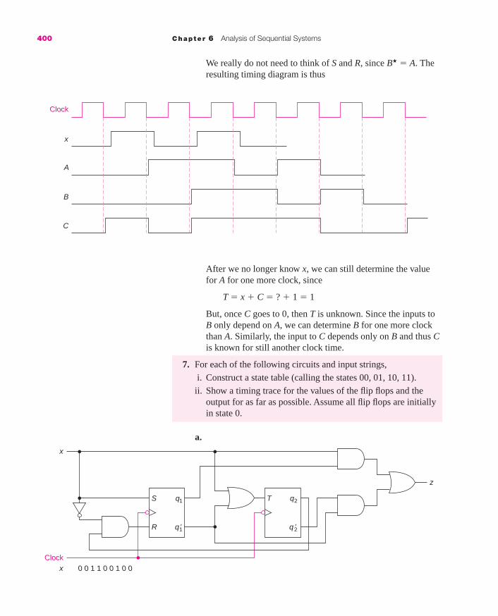
We really do not need to think of S and R, since B� � A. Theresulting timing diagram is thus
Clock
x
A
B
C
After we no longer know x, we can still determine the valuefor A for one more clock, since
T � x � C � ? � 1 � 1
But, once C goes to 0, then T is unknown. Since the inputs toB only depend on A, we can determine B for one more clockthan A. Similarly, the input to C depends only on B and thus Cis known for still another clock time.
7. For each of the following circuits and input strings,
i. Construct a state table (calling the states 00, 01, 10, 11).
ii. Show a timing trace for the values of the flip flops and theoutput for as far as possible. Assume all flip flops are initiallyin state 0.
x
z
T q2
q1�R q 2�
S q1
Clockx 0 0 1 1 0 0 1 0 0
a.
400 Chapter 6 Analysis of Sequential Systems
mar91647_c06d_399_403.qxd 11/14/08 11:14 AM Page 400
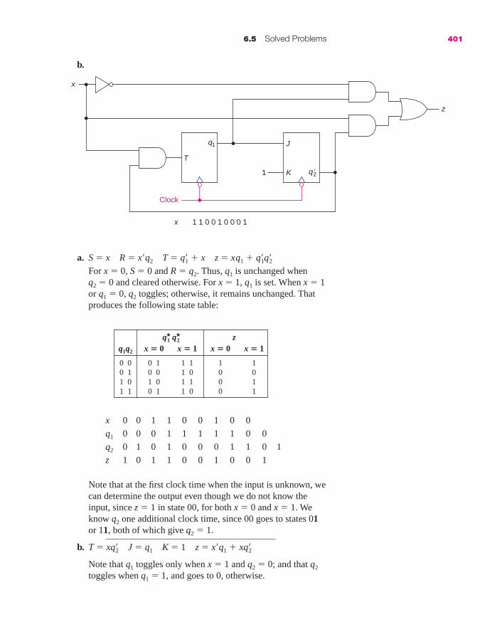
a. S � x R � x�q2 T � q�1 � x z � xq1 � q�1q�2For x � 0, S � 0 and R � q2. Thus, q1 is unchanged whenq2 � 0 and cleared otherwise. For x � 1, q1 is set. When x � 1or q1 � 0, q2 toggles; otherwise, it remains unchanged. Thatproduces the following state table:
6.5 Solved Problems 401
Clock
x 1 1 0 0 1 0 0 0 1
J
q2�K1
q1
T
x
z
b.
q1� q2
� zq1q2 x � 0 x � 1 x � 0 x � 1
0 0 0 1 1 1 1 10 1 0 0 1 0 0 01 0 1 0 1 1 0 11 1 0 1 1 0 0 1
x 0 0 1 1 0 0 1 0 0
q1 0 0 0 1 1 1 1 1 0 0
q2 0 1 0 1 0 0 0 1 1 0 1
z 1 0 1 1 0 0 1 0 0 1
Note that at the first clock time when the input is unknown, wecan determine the output even though we do not know theinput, since z � 1 in state 00, for both x � 0 and x � 1. Weknow q2 one additional clock time, since 00 goes to states 01or 11, both of which give q2 � 1.
b. T � xq�2 J � q1 K � 1 z � x�q1 � xq�2
Note that q1 toggles only when x � 1 and q2 � 0; and that q2
toggles when q1 � 1, and goes to 0, otherwise.
mar91647_c06d_399_403.qxd 11/14/08 11:14 AM Page 401

x 1 1 0 0 1 0 0 0 1 1
q1 0 1 0 0 0 1 1 1 1 1 0 0
q2 0 0 1 0 0 0 1 0 1 0 1 0 0
z 1 1 0 0 1 1 1 1 0 1 0
In this example, we can determine the state for two clocksafter the input is no longer known, the value of q2 for a third(since from state 00, we go either to 00 or 10) and the outputfor one clock after the last known input.
8. For the following circuits, complete the timing trace as far aspossible. The state of some flip flops can be determined as manyas five or six clocks after the input is no longer known. Assumethat all flip flops are initially 0.
a.
q1� q2
� zq1q2 x � 0 x � 1 x � 0 x � 1
0 0 0 0 1 0 0 10 1 0 0 0 0 0 01 0 1 1 0 1 1 11 1 1 0 1 0 1 0
B� C�A�K
T B DJx A
Clock
x 0 1 1 1
C
K q3�q 2�R
J
x
S q2
Clock
x 0 1 1 1 0 0 1
T
q4D q1
b.
402 Chapter 6 Analysis of Sequential Systems
mar91647_c06d_399_403.qxd 11/14/08 11:14 AM Page 402
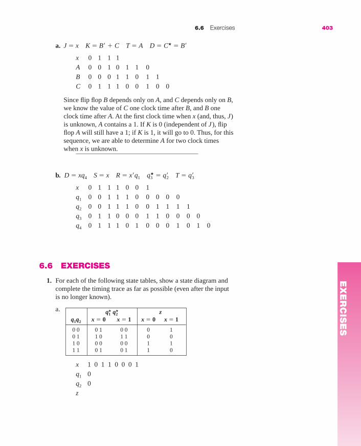
a. J � x K � B� � C T � A D � C� � B�
x 0 1 1 1
A 0 0 1 0 1 1 0
B 0 0 0 1 1 0 1 1
C 0 1 1 1 0 0 1 0 0
Since flip flop B depends only on A, and C depends only on B,we know the value of C one clock time after B, and B oneclock time after A. At the first clock time when x (and, thus, J)is unknown, A contains a 1. If K is 0 (independent of J ), flipflop A will still have a 1; if K is 1, it will go to 0. Thus, for thissequence, we are able to determine A for two clock timeswhen x is unknown.
b. D � xq4 S � x R � x�q1 q3� � q�2 T � q�3
x 0 1 1 1 0 0 1
q1 0 0 1 1 1 0 0 0 0 0
q2 0 0 1 1 1 0 0 1 1 1 1
q3 0 1 1 0 0 0 1 1 0 0 0 0
q4 0 1 1 1 0 1 0 0 0 1 0 1 0
6.6 Exercises 403
6.6 EXERCISES
1. For each of the following state tables, show a state diagram andcomplete the timing trace as far as possible (even after the inputis no longer known).
a. q1★ q2
★ zq1q2 x � 0 x � 1 x � 0 x � 1
0 0 0 1 0 0 0 10 1 1 0 1 1 0 01 0 0 0 0 0 1 11 1 0 1 0 1 1 0
x 1 0 1 1 0 0 0 1
q1 0
q2 0
z
EX
ER
CIS
ES
mar91647_c06d_399_403.qxd 11/14/08 11:14 AM Page 403

404 Chapter 6 Analysis of Sequential Systems
★b. q★
q x � 0 x � 1 z
A A B 0B C B 0C A D 0D C B 1
x 1 1 0 1 0 1 0 1 0 0 1 0 1 1
q A
z
c. q★ zq x � 0 x � 1 x � 0 x � 1
A B C 0 1B C A 0 0C A B 1 0
q★ zq x � 0 x � 1 x � 0 x � 1
A A B 1 0B C D 0 0C A B 0 0D C D 1 0
x 0 0 1 1 1 0 0 0 0 0 1 0
q A
z
d.
x 0 1 0 0 0 1 1 1 1 0 1
q A
z
2. Show the block diagram for a gated latch that behaves similarlyto the one of Figure 6.6, but uses only NAND gates.
EX
ER
CIS
ES
mar91647_c06e_404_414.qxd 11/14/08 11:20 AM Page 404

3. For the input shown below, show the flip flop outputs.
a. Assume that the flip flop is a D flip flop without a clear orpreset.
b. Assume that the flip flop is a D flip flop with an active lowclear.
c. Assume that the flip flop is a D flip flop with active low clearand preset inputs.
d. Assume that the flip flop is a T flip flop with the same input aspart a, and that Q is initially 0.
e. Assume that the flip flop is a T flip flop with an active low clearand the same inputs as part b.
6.6 Exercises 405
Clock
D or T
CLR�
CLR�
PRE �
4. For the following JK flip flops, complete each of the timingdiagrams. First, assume that CLR� and PRE� are inactive (1).Then, use the values shown.
Clock
J
K
q
q�
CLR�
PRE�
b. and e.
c.
EX
ER
CIS
ES
mar91647_c06e_404_414.qxd 11/14/08 11:20 AM Page 405

406 Chapter 6 Analysis of Sequential Systems
5. Consider the following flip flop circuit
a.
b.
★c.
Clock
J
K
CLR�
J
K
CLR�
PRE�
Q
CLR�
J
K
Clock
IN Q�
x
Q
Complete the timing diagram below if that flip flop is
a. a D flip flop
b. a T flip flop
In both cases, the flip flop starts with a 0 in it.
Clock
x
EX
ER
CIS
ES
mar91647_c06e_404_414.qxd 11/14/08 11:20 AM Page 406
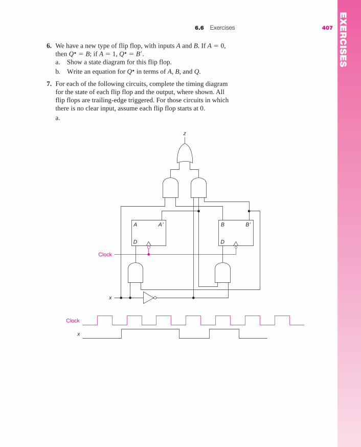
6. We have a new type of flip flop, with inputs A and B. If A � 0,then Q★ � B; if A � 1, Q★ � B�.a. Show a state diagram for this flip flop.
b. Write an equation for Q★ in terms of A, B, and Q.
7. For each of the following circuits, complete the timing diagramfor the state of each flip flop and the output, where shown. Allflip flops are trailing-edge triggered. For those circuits in whichthere is no clear input, assume each flip flop starts at 0.
a.
6.6 Exercises 407
Clock
A
D
A� B
D
B�
x
z
Clock
x
EX
ER
CIS
ES
mar91647_c06e_404_414.qxd 11/14/08 11:20 AM Page 407

★b.
d.
408 Chapter 6 Analysis of Sequential Systems
T q1
q1�
S zx
R
q2
q 2�
Clock
Clock
x
S q1
q 1�
Dx
R
q2
q2�
J
K
q3
q3�
Clock
CLR�
CLR�
Clock
x
D q1
q1�
J
K
q2
q2�
z
x
Clock
Clock
x
c.
EX
ER
CIS
ES
mar91647_c06e_404_414.qxd 11/14/08 11:20 AM Page 408

8. For each of the following circuits and input strings
i. Construct a state table (calling the states 00, 01, 10, 11).
ii. Show a timing trace for the values of the flip flops and theoutput for as far as possible. Assume that the initial value ofeach flip flop is 0.
★a.
6.6 Exercises 409
D q1
q1�
D q2
q2�
z
x
Clock
x 0 0 1 1 0 0 1 1 0
b.
J B
B�K
J A
A�K
x
Clock
x 0 0 1 1 0 0 1 1 0
z
EX
ER
CIS
ES
mar91647_c06e_404_414.qxd 11/14/08 11:20 AM Page 409

410 Chapter 6 Analysis of Sequential Systems
d.
q1 q1�
S R
Clock
x 0 0 1 1 0 0 1 1 0
x
z
q2 q 2�
T
c.
J q1
q 1�K K
J q2
z
x
Clock
x 0 1 1 0 1 1 1 1 1
EX
ER
CIS
ES
mar91647_c06e_404_414.qxd 11/14/08 11:20 AM Page 410

9. For the following circuits, complete the timing trace as far aspossible. The state of some flip flops and the output can be determined for as many as three clocks after the input is nolonger known. Assume that all flip flops are initially 0.
6.6 Exercises 411
C �RK
S C
B�
T B
z
x J A
Clock
x 0 1 1 0 1 0 1
R
S C
B�
T Bx
D A
Clock
x 0 1 0 1 0 1 0
b.
a.
EX
ER
CIS
ES
mar91647_c06e_404_414.qxd 11/14/08 11:20 AM Page 411

412 Chapter 6 Analysis of Sequential Systems
6.7 CHAPTER 6 TEST (50 MINUTES)
1. For the following state table, complete the timing trace as far asyou can.
q★ zq x � 0 x � 1 x � 0 x � 1
A C A 0 0B A D 1 1C B C 0 1D B B 0 0
x 0 0 1 1 0 0 0 1 0 1
q A
z
d.
R
D q3
q2�q1�K q3�
S q2x J q1
Clock
x 0 0 1 0 0 0
★c.
RK
S C
B�A� C�
J B
x
T A
Clock
x 0 1 1 0 0 1 1 1 0
z EX
ER
CIS
ES
CH
AP
TE
R T
ES
T
mar91647_c06e_404_414.qxd 11/14/08 11:20 AM Page 412

2. For the following JK trailing-edge triggered flip flop with an active low clear, show the timing diagram for Q.
a. Assuming no CLR� input.
b. With the CLR� input shown.
6.7 Chapter 6 Test 413
J
Q�
CLR�
K
Clock
Q
K
J
Q
Q
CLR�
Clock
3. For the following circuit, construct the state table.
B�
T B
x
Clock
A�
D A
z
a.
b.
CH
AP
TE
R T
ES
T
mar91647_c06e_404_414.qxd 11/14/08 11:20 AM Page 413
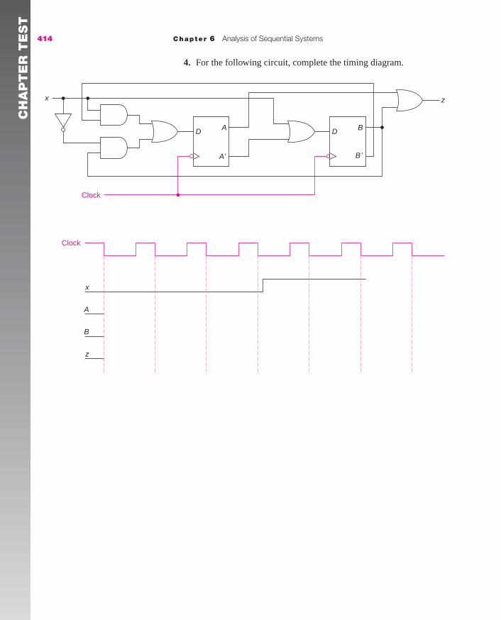
414 Chapter 6 Analysis of Sequential Systems
4. For the following circuit, complete the timing diagram.
B�
D B
x
Clock
A�
D A
z
x
A
B
z
Clock
CH
AP
TE
R T
ES
T
mar91647_c06e_404_414.qxd 11/14/08 11:20 AM Page 414

415
*This is very similar to CE6 (introduced in Chapter 6), except that the output goes to 1simultaneously with the third consecutive 1 (whereas in CE6, the system went to a statewith a 1 output when it received the third 1).
C H A P T E R
7The Design ofSequential Systems
As in the case of combinational systems, the design process typi-cally starts with a problem statement, a verbal description of theintended behavior of the system. The goal is to develop a block
diagram of the system utilizing the available components and meetingthe design objectives and constraints.
We will first present five additional Continuing Examples, which wewill use throughout the chapter to illustrate the design techniques.
Continuing Examples (CE)
CE7. A Mealy system with one input x and one output z such that z � 1at a clock time iff x is currently 1 and was also 1 at the previous two clocktimes.*
CE8. A Moore system with one input x and one output z, the output ofwhich is 1 iff three consecutive 0 inputs occurred more recently than threeconsecutive 1 inputs.
CE9. A system with no inputs and three outputs, that represent a numberfrom 0 to 7, such that the outputs cycle through the sequence 0 3 2 4 1 5 7 and repeat on consecutive clock inputs.
CE10. A system with two inputs, x1 and x2, and three outputs, z1, z2, andz3, that represent a number from 0 to 7, such that the output counts up ifx1 � 0 and down if x1 � 1, and recycles if x2 � 0 and saturates if x2 � 1.Thus, the following output sequences might be seen
x1 � 0, x2 � 0: 0 1 2 3 4 5 6 7 0 1 2 3 4 5 6 7 . . .
x1 � 0, x2 � 1: 0 1 2 3 4 5 6 7 7 7 7 7 7 7 7 7 . . .
x1 � 1, x2 � 0: 7 6 5 4 3 2 1 0 7 6 5 4 3 2 1 0 . . .
x1 � 1, x2 � 1: 7 6 5 4 3 2 1 0 0 0 0 0 0 0 0 0 . . .
mar91647_c07a_415_465.qxd 11/24/08 12:01 PM Page 415

(Of course, x1 and x2 may change at some point so that the output wouldswitch from one sequence to another.)
CE11. A bus controller that receives requests on separate lines, R0 to R3,from four devices desiring to use the bus. It has four outputs, G0 to G3,only one of which is 1, indicating which device is granted control of thebus for that clock period. (We will consider, in Section 7.4, the design forsuch a priority controller, where the low number device has the highestpriority, if more than one device requests the bus at the same time. Welook at both interrupting controllers, where a high priority device canpreempt the bus, and one where a device keeps control of the bus once it gets control until it no longer needs the bus.)
In addition to these Continuing Examples, there are three additionalcomplete examples (from verbal description to final design) in Appen-dix E.2.
We will next look at the design process for systems similar to thosethat we just described. In Chapter 8, we will look at some other tech-niques that are suitable for larger systems.
Sometimes there may be different ways of storing the necessary infor-mation. For CE7, we could just store the last two values of the input. If weknow that and we know the current input, then we know if all three havebeen 1. But we could also store how many consecutive 1’s there havebeen—none, one, or two or more. We can develop the state table either way;each will produce a properly working circuit. However, the cost might bequite different. Just consider what would have been the case if we wanted anoutput of 1 iff the input was now 1 and was also 1 for the last 27 consecutiveclocks. The first approach would require us to store the last 27 inputs—in27 flip flops. The second approach would require us to keep track of only28 things, 0 consecutive 1’s through 27 or more consecutive 1’s. But 28 factscan be stored using only five binary storage devices, coding none as 00000,through 27 or more as 11011 (the binary equivalent of 27).
This is the same problem as for combinational systems. Many prob-lems are stated in such a way that this step is not necessary.
Step 3: Derive a state table or state diagram to describe thebehavior of the system.
Step 2: If necessary, code the inputs and outputs in binary.
Step 1: From a word description, determine what needs to bestored in memory. That is, what are the possible states?
416 Chapter 7 The Design of Sequential Systems
mar91647_c07a_415_465.qxd 11/24/08 12:01 PM Page 416

In Moore systems, such as CE6 and CE8, the output depends onlyon the present state of the system. (The combinational logic that pro-duces the output is just a function of the contents of the various flipflops.) (The output does, of course, depend on the input, since the statedepends on the input, but the effect on the output is delayed until after thenext clock.) In other examples, such as CE7, the output depends on thecurrent input as well as the contents of memory.
Fewer states may mean fewer storage devices. By reducing the num-ber of flip flops, we also reduce the number of inputs to the combina-tional logic. Thus, for example, a system with one input and three flipflops requires four-variable combinational logic, whereas one withtwo flip flops would use only three-variable logic. This usually means aless expensive circuit. (This step could be omitted and a correctly work-ing system designed.)
Any coding will do, that is, will produce a correct solution. However, agood choice will often lead to simpler combinational logic (see Chapter 9).
The state table and state assignment produce a table that tells whatis to be stored in each flip flop as a function of what is in memory nowand the system input. This part of the problem is to determine what inputmust be applied to each flip flop to get that transition to take place. In thischapter, we will look at the technique that is required for the varioustypes of flip flops commonly used.
Step 7: Produce the logic equation and draw a block diagram (as inthe case of combinational systems).
Step 6: Choose a flip flop type and derive the flip flop input maps ortables.
Step 5: Choose a state assignment, that is, code the states inbinary.
Step 4: Use state reduction techniques (see Chapter 9)* to find astate table that produces the same input/output behavior but hasfewer states.
Chapter 7 The Design of Sequential Systems 417
*Chapter 9 is available on the student side of the book’s Web site,http://www.mhhe.com/marcovitz.
mar91647_c07a_415_465.qxd 11/24/08 12:01 PM Page 417

In this chapter, we will be concerned first with Steps 6 and 7; then,we will return to Step 1. In Chapter 9, we will develop techniques forstate reduction (Step 4) and state assignment (Step 5).
The state table of Table 6.1 and the state diagram of Figure 6.3 arerepeated here as Figure 7.1.
418 Chapter 7 The Design of Sequential Systems
Three state assignments are shown in Table 7.1.*
1
00 0
11B0
C0
0
A0
D1
1
*We will demonstrate in Chapter 9 that all of the other possible state assignments result inthe same amount of combinational logic as one of these. Each can be obtained either by arenumbering of the flip flops or the replacement of variables by their complement or both.
Table 7.1 State assignments.
q q1 q2 q q1 q2 q q1 q2
A 0 0 A 0 0 A 0 0B 0 1 B 1 1 B 0 1C 1 0 C 1 0 C 1 1D 1 1 D 0 1 D 1 0
(a) (b) (c)
These assignments were chosen arbitrarily. It is not clear which choicemight lead to the least combinational logic.
From either the state diagram or the state table, we construct thedesign truth table of Table 7.2 for the next state. For this first example,we will use the state assignment of Table 7.1a.
Although the q column is not really needed, it is helpful in thedevelopment of the truth table, particularly if the states are assigned insome order other than numerical (such as in Tables 7.1b and 7.1c). Thefirst half of the design truth table corresponds to the first column of thestate table (x � 0). The next state is 00 for the first four rows, since eachof the states go to state A on a 0 input. The second half of the table cor-responds to x � 1.
For a Moore system, we construct a separate table for the output(Table 7.3), since it depends only on the two state variables. (As we will
Table 7.2 Design truth table.
q x q1 q2 q1� q2
�
A 0 0 0 0 0B 0 0 1 0 0C 0 1 0 0 0D 0 1 1 0 0A 1 0 0 0 1B 1 0 1 1 0C 1 1 0 1 1D 1 1 1 1 1
q�
q x � 0 x � 1 z
A A B 0B A C 0C A D 0D A D 1
Figure 7.1 Design example.
mar91647_c07a_415_465.qxd 11/26/08 9:57 AM Page 418

see shortly, the z column would be included as another column in thedesign truth table for a Mealy system.)
We can now map q1�, q2
�, and z, as shown in Map 7.1. We prefer todraw the Karnaugh maps in the vertical orientation for such problemssince the columns correspond to the input and the rows to the states.
Chapter 7 The Design of Sequential Systems 419
Table 7.3 Output truth table.
q q1 q2 z
A 0 0 0B 0 1 0C 1 0 0D 1 1 1
0 1
00
01
11
10
x
q1 q2
1
1
1
0 1
00
01
11
10
x
q1 q2
1
1
1
0
z
1
0
1
q1
q2
1
Map 7.1 Next state and output maps.
We thus have the equations
q1� � xq2 � xq1
q2� � xq�2 � xq1
z � q1q2
(Although we took advantage of the obvious sharing available in thisexample, we will not emphasize sharing in the development of flip flopinput equations.) Note that this sum of products solution requires 4 two-input AND gates and 2 two-input OR gates (or 6 two-input NAND gatesplus a NOT, since z comes from an AND, requiring a NAND followed bya NOT).*
If we use the state assignment of Table 7.1b, we get the following designtruth table:
*We assumed that q1 and q2 are available both uncomplemented and complemented, but xis only available uncomplemented (although the latter is irrelevant in this example).
EXAMPLE 7.1
q1� q2
�
x q1 q2 q1� q2
� q q1 q2 z
A 0 0 0 0 0 A 0 0 0D 0 0 1 0 0 D 0 1 1C 0 1 0 0 0 C 1 0 0B 0 1 1 0 0 B 1 1 0A 1 0 0 1 1D 1 0 1 0 1C 1 1 0 0 1B 1 1 1 1 0
mar91647_c07a_415_465.qxd 11/24/08 12:01 PM Page 419
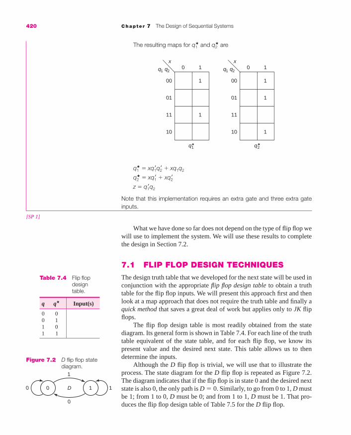
420 Chapter 7 The Design of Sequential Systems
q1� � xq1�q2� � xq1q2
q2� � xq1� � xq2�
z � q1�q2
Note that this implementation requires an extra gate and three extra gateinputs.
What we have done so far does not depend on the type of flip flop wewill use to implement the system. We will use these results to completethe design in Section 7.2.
7.1 FLIP FLOP DESIGN TECHNIQUES
The design truth table that we developed for the next state will be used inconjunction with the appropriate flip flop design table to obtain a truthtable for the flip flop inputs. We will present this approach first and thenlook at a map approach that does not require the truth table and finally aquick method that saves a great deal of work but applies only to JK flipflops.
The flip flop design table is most readily obtained from the statediagram. Its general form is shown in Table 7.4. For each line of the truthtable equivalent of the state table, and for each flip flop, we know itspresent value and the desired next state. This table allows us to thendetermine the inputs.
Although the D flip flop is trivial, we will use that to illustrate theprocess. The state diagram for the D flip flop is repeated as Figure 7.2.The diagram indicates that if the flip flop is in state 0 and the desired nextstate is also 0, the only path is D � 0. Similarly, to go from 0 to 1, D mustbe 1; from 1 to 0, D must be 0; and from 1 to 1, D must be 1. That pro-duces the flip flop design table of Table 7.5 for the D flip flop.
The resulting maps for q1� and q2
� are
0 1
00
01
11
10
x
q1 q2
1
1
0 1
00
01
11
10
x
q1 q2
1
1
1
q1★ q2
★
[SP 1]
Table 7.4 Flip flopdesigntable.
q q� Input(s)
0 00 11 01 1
Figure 7.2 D flip flop statediagram.
0 1
1
D
0
0 1
mar91647_c07a_415_465.qxd 11/24/08 12:01 PM Page 420

7.1 Flip Flop Design Techniques 421
For the D flip flop, we do not need separate columns in the truthtable for D1 and D2, since they are identical to the q1
� and q2� columns. We
will use the design table of Table 7.2 as an example throughout this sec-tion. Thus, for D flip flops,
D1 � x q2 � x q1
D2 � x q2� � x q1
A block diagram of the solution, using D flip flops and AND and ORgates, is shown in Figure 7.3.
We will now repeat the process for the JK flip flop. The state dia-gram for the JK flip flop is repeated as Figure 7.4. To go from state 0 tostate 0, we have two choices; we can make J � 0 and K � 0, or J � 0and K � 1. In other words, J must be 0 and it does not matter what K is,that is, K is a don’t care. Similarly, to go from 1 to 1, K must be 0 and Jis a don’t care. To go from 0 to 1, J must be 1 and K is a don’t care andto go from 1 to 0, K must be 1 and J is a don’t care. This results in theJK flip flop design table of Table 7.6. The truth table for the systemdesign is thus shown in Table 7.7. Now, the truth table for the designrequires four more columns for the four flip flop inputs. (The q columnwith state names has been omitted since the first five columns of thistable are identical to the corresponding columns of Table 7.2.) Theshaded columns, q1 and q1
�, produce the shaded flip flop input columns,using Table 7.6. The unshaded columns (for flip flop 2) produce theunshaded flip flop inputs. In each of the first two rows, q1 goes from 0 to 0;thus, from the first row of the flip flop design table, J1 � 0 and K1 � X.In the first row, q2 also goes from 0 to 0, producing J2 � 0 and K2 � X.
Figure 7.3 Implementation using D flip flops.
q1
q1�
D
Clock
q2
q 2�
D
z
x
Figure 7.4 JK flip flop statediagram.
0001
0010
1011
J K
0111
0 1
Table 7.6 JK flip flopdesign table.
q q� J K
0 0 0 X0 1 1 X1 0 X 11 1 X 0
Table 7.5 D flip flopdesign table.
q q� D
0 0 00 1 11 0 01 1 1
mar91647_c07a_415_465.qxd 11/24/08 12:01 PM Page 421
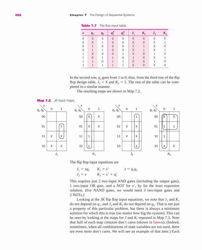
422 Chapter 7 The Design of Sequential Systems
In the second row, q2 goes from 1 to 0; thus, from the third row of the flipflop design table, J2 � X and K2 � 1. The rest of the table can be com-pleted in a similar manner.
The resulting maps are shown in Map 7.2.
Table 7.7 Flip flop input table.
x q1 q2 q1� q2
� J1 K1 J2 K2
0 0 0 0 0 0 X 0 X0 0 1 0 0 0 X X 10 1 0 0 0 X 1 0 X0 1 1 0 0 X 1 X 11 0 0 0 1 0 X 1 X1 0 1 1 0 1 X X 11 1 0 1 1 X 0 1 X1 1 1 1 1 X 0 X 0
Map 7.2 JK input maps.
0 1
00
01
11
10
x
q1 q2
J1 K1
X
X
X
X
1
0 1
00
01
11
10
x
q1 q2
X
XX
X
1
1
J2
0 1
1
1
00
01
11
10
x
q1 q2
X X
X X
XX
XX
K2
0 1
00
01
10
10
x
q1 q2
1
1
1
The flip flop input equations are
J1 � xq2 K1 � x� z � q1q2
J2 � x K2 � x� � q�1
This requires just 2 two-input AND gates (including the output gate),1 two-input OR gate, and a NOT for x�, by far the least expensivesolution. (For NAND gates, we would need 3 two-input gates and2 NOTs.)
Looking at the JK flip flop input equations, we note that J1 and K1
do not depend on q1, and J2 and K2 do not depend on q2. That is not justa property of this particular problem, but there is always a minimumsolution for which this is true (no matter how big the system). This canbe seen by looking at the maps for J and K, repeated in Map 7.3. Notethat half of each map contains don’t cares (shown in brown). (Indeed,sometimes, when all combinations of state variables are not used, thereare even more don’t cares. We will see an example of that later.) Each
mar91647_c07a_415_465.qxd 11/24/08 12:01 PM Page 422

7.1 Flip Flop Design Techniques 423
0 1
00
01
11
10
x
q1 q2
J1 K1
X X
XX
1
0 1
00
01
11
10
x
q1 q2
1
XX
XX
1
0 1
00
01
11
10
x
q1 q2
J2 K2
X
XX
X
1
1
0 1
00
01
10
10
x
q1 q2
1
1 1
X
XX
X
x q2 x � q2�
x � q2
x q1�
x q1
x � q1�
x � q1x q1�
Map 7.3 Pairing of 1’s and don’t cares in JK flip flop inputs.
of the 1’s on the map has a don’t care in such a position that the 1 canbe combined with the don’t care to eliminate the variable involved.These are shown circled on the maps and the terms listed below. Theseterms are not necessarily prime implicants, but those for J1 and K1 donot involve q1, and those for J2 and K2 do not involve q2.
In Examples 7.2 and 7.3, we will repeat this process for the SR andT flip flops.
The state diagram for the SR flip flop is repeated below.
To go from state 0 to state 0 or from state 1 to state 1, we have the sametwo choices as for the JK. To go from 0 to 1, S must be 1 and R must be 0,and to go from 1 to 0, R must be 1 and S must be 0. The resulting SR flipflop design table is
0001
0010
10
S R
01
0 1
EXAMPLE 7.2
q q� S R
0 0 0 X0 1 1 01 0 0 11 1 X 0
Note that S and R will never both be made 1 (whatever values we choosefor the don’t cares). Following the same technique as for JK flip flops, we get
mar91647_c07a_415_465.qxd 11/24/08 12:01 PM Page 423
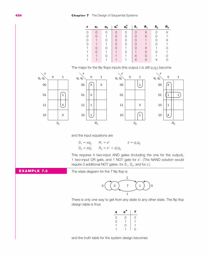
424 Chapter 7 The Design of Sequential Systems
0 1
00
01
11
10
x
q1 q2
S1 R1
X
X
1
0 1
00
01
11
10
x
q1 q2
X
X
X
1
1
S2
0 1
1
1
00
01
11
10
x
q1 q2
X
X
X
R2
0 1
00
01
10
10
x
q1 q2
1
1
1
x q1 q2 q1� q2
� S1 R1 S2 R2
0 0 0 0 0 0 X 0 X0 0 1 0 0 0 X 0 10 1 0 0 0 0 1 0 X0 1 1 0 0 0 1 0 11 0 0 0 1 0 X 1 01 0 1 1 0 1 0 0 11 1 0 1 1 X 0 1 01 1 1 1 1 X 0 X 0
The maps for the flip flops inputs (the output z is still q1q2) become
and the input equations are
S1 � xq2 R1 � x� z � q1q2
S2 � xq�2 R2 � x� � q�1q2
This requires 4 two-input AND gates (including the one for the output), 1 two-input OR gate, and 1 NOT gate for x�. (The NAND solution wouldrequire 3 additional NOT gates, for S1, S2, and for z.)
The state diagram for the T flip flop is
There is only one way to get from any state to any other state. The flip flopdesign table is thus
0 0
1
T
1
0 1
EXAMPLE 7.3
and the truth table for the system design becomes
q q� T
0 0 00 1 11 0 11 1 0
mar91647_c07a_415_465.qxd 11/24/08 12:01 PM Page 424

7.1 Flip Flop Design Techniques 425
The maps for T and the equations are shown below.
0 1
00
01
11
10
x
q1 q2
T1 T2
1
1
1
0 1
00
01
11
10
x
q1 q2
1
1
1
1
1
x q1 q2 q1� q2
� T1 T2
0 0 0 0 0 0 00 0 1 0 0 0 10 1 0 0 0 1 00 1 1 0 0 1 11 0 0 0 1 0 11 0 1 1 0 1 11 1 0 1 1 0 11 1 1 1 1 0 0
T1 � x�q1 � xq�1q2
T2 � x�q2 � xq�2 � xq�1q2
z � q1q2
This requires 4 two-input AND gates, 1 three-input AND gate, 1 two-inputand 1 three-input OR gate, and a NOT for x. This is the most expensivesolution for this example. (But, there are systems for which the T will resultin a less expensive circuit than D or SR.)
The JK solution never requires more logic than either the SR or theT. Comparing the maps for the SR and the JK solutions, we see that bothmaps have 1’s in exactly the same places. Further, all of the X’s in the SRsolution are also X’s on the JK maps. The JK maps have additional don’tcares. We could always choose to make those don’t cares 0 and arrive atthe SR solution. But, as we saw above, some of those X’s were useful tomake larger groupings and thus simplify the logic. From a different pointof view, say we were to design a system for SR flip flops and build thecombinational logic. If we then found that all we had available withwhich to build it was JK flip flops, we could use the logic and it wouldwork. Similarly, if we designed for T flip flops, we could connect thatlogic to both J and K; the JK flip flop would behave like a T. (As in thecase of the SR, there is often more logic required this way.) The
mar91647_c07a_415_465.qxd 11/24/08 12:01 PM Page 425
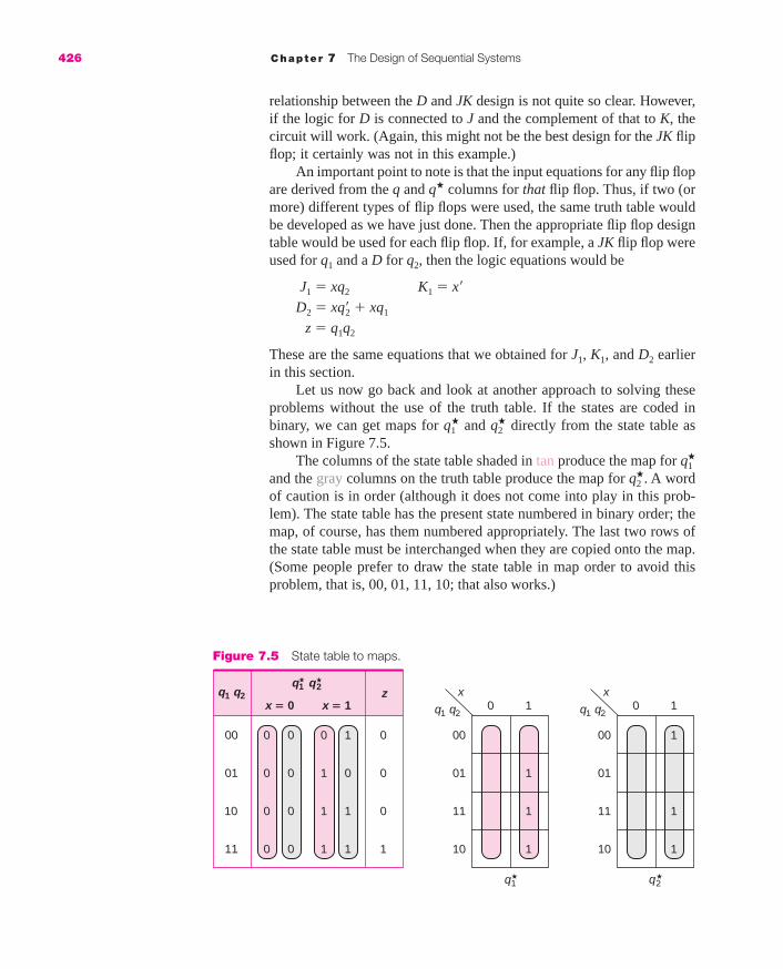
426 Chapter 7 The Design of Sequential Systems
relationship between the D and JK design is not quite so clear. However,if the logic for D is connected to J and the complement of that to K, thecircuit will work. (Again, this might not be the best design for the JK flipflop; it certainly was not in this example.)
An important point to note is that the input equations for any flip flopare derived from the q and q� columns for that flip flop. Thus, if two (ormore) different types of flip flops were used, the same truth table wouldbe developed as we have just done. Then the appropriate flip flop designtable would be used for each flip flop. If, for example, a JK flip flop wereused for q1 and a D for q2, then the logic equations would be
J1 � xq2 K1 � x�
D2 � xq�2 � xq1
z � q1q2
These are the same equations that we obtained for J1, K1, and D2 earlierin this section.
Let us now go back and look at another approach to solving theseproblems without the use of the truth table. If the states are coded inbinary, we can get maps for q1
� and q2� directly from the state table as
shown in Figure 7.5. The columns of the state table shaded in tan produce the map for q1
�
and the gray columns on the truth table produce the map for q2�. A word
of caution is in order (although it does not come into play in this prob-lem). The state table has the present state numbered in binary order; themap, of course, has them numbered appropriately. The last two rows ofthe state table must be interchanged when they are copied onto the map.(Some people prefer to draw the state table in map order to avoid thisproblem, that is, 00, 01, 11, 10; that also works.)
0 1
00
01
11
10
x
q1 q2
q1 q2
1
1
1
0 1
00
01
11
10
x
q1 q2
1
1
1
zx � 1x � 0
0
0
0
1
00
01
10
11
0 1
0
1
1
0
0
0
0
1
1
1
0
0
0
0
q1★ q2
★
q1★ q2
★
Figure 7.5 State table to maps.
mar91647_c07a_415_465.qxd 11/24/08 12:01 PM Page 426
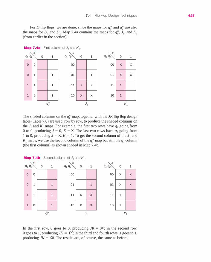
7.1 Flip Flop Design Techniques 427
0 1
0
1
1
0
xq1 q2
J1
1
1
1
0 1
00
01
11
10
xq1 q2
1
XX
XX
K1
0 1
1
1
00
01
11
10
xq1 q2
X X
XX
0
1
1
0
q1★
Map 7.4a First column of J1 and K1.
The shaded columns on the q1� map, together with the JK flip flop design
table (Table 7.6) are used, row by row, to produce the shaded columns onthe J1 and K1 maps. For example, the first two rows have q1 going from 0 to 0, producing J � 0, K � X. The last two rows have q1 going from 1 to 0, producing J � X, K � 1. To get the second column of the J1 andK1 maps, we use the second column of the q1
� map but still the q1 column(the first column) as shown shaded in Map 7.4b.
0 1
0
1
1
0
xq1 q2
J1
1
1
1
0 1
00
01
11
10
xq1 q2
1
XX
XX
K1
0 1
1
1
00
01
11
10
xq1 q2
X X
XX
0
1
1
0
q1★
Map 7.4b Second column of J1 and K1.
In the first row, 0 goes to 0, producing JK � 0X; in the second row,0 goes to 1, producing JK � 1X; in the third and fourth rows, 1 goes to 1,producing JK � X0. The results are, of course, the same as before.
For D flip flops, we are done, since the maps for q1� and q2
� are alsothe maps for D1 and D2. Map 7.4a contains the maps for q1
�, J1, and K1
(from earlier in the section).
mar91647_c07a_415_465.qxd 11/24/08 12:01 PM Page 427

428 Chapter 7 The Design of Sequential Systems
0 1
0
0
1
1
xq1 q2
J2
1
1
1
0 1
00
01
11
10
xq1 q2
1
1
X
X
K2
0 1
1
1 1
00
01
10
10
xq1 q2
X
XX
X
1
1
0
0
X
X
q2★
Map 7.4c Computation of J2 and K2.
To find J and K for flip flop q2, we map q2� and use the q2 column, as
shown in the shading for the first column of J2 and K2 in Map 7.4c. Wethen use the same column of q2 with the other column of the q2
� map toform the second columns of the J2 and K2 maps.
This same technique can be used with the other type of flip flops(using the appropriate flip flop design table). Caution: The q1 input (thefirst input column) is used with both the first and second columns of q1
�
to obtain the inputs to the first flip flop. The q2 input (the second inputcolumn) is used with both the first and second columns of q2
� to obtainthe inputs to the second flip flop.
The quick method for JK flip flop design (it does not apply to theother types of flip flop) takes advantage of a property of the JK flip flopinput equations, where J1 and K1 do not depend on q1, and J2 and K2 donot depend on q2. That is not just a property of this particular problem,but there is always a minimum solution for which this is true (no matterhow big the system).
We can take advantage of this property by utilizing the equation wedeveloped in Section 6.3,
q� � Jq� � K�q
Notice that when q � 0,
q� � J · 1 � K� · 0 � J
and when q � 1,
q� � J · 0 � K� · 1 � K�.
Thus, the part of the map of q� (for each variable) for which that vari-able is 0 is the map for J and the part for which that variable is 1 is themap for K�. On Map 7.5a, we show q1
� with the q1 � 0 section shaded in
mar91647_c07a_415_465.qxd 11/24/08 12:01 PM Page 428

7.1 Flip Flop Design Techniques 429
tan and the q1 � 1 section shaded in gray. The two smaller maps are thencopied separately to the right. (That is not really necessary; we couldwork on the separate sections of the larger map.)
The three variable map has been reduced to 2 two-variable maps, one forJ and the other for K�. The variable q1 has been eliminated; that was usedto choose the section of the original map. (We could have drawn the mapfor K; it would just require replacing 0’s by 1’s and 1’s by 0’s.) Fromthese maps, we see
J1 � xq2 K�1 � x or K1 � x�
These are, of course, the same answer we obtained using the other meth-ods as in Map 7.2 and Maps 7.4a and 7.4b. Be careful in using the mapfor K�1; the two rows are reversed, that is, the q2 � 1 row is on the top.That does not affect this problem and just requires care in reading themap in other problems. (We could redraw the map and interchange therows.)
We will repeat this process for the second flip flop on Map 7.5b,since the map geometry is somewhat different.
0 1
0
0
1
1
xq1 q2
J2 K 2� K2
1
1
1
0 1
0
1
xq1
1
1
1
1
0
0
0 1
0
1
xq1
1
0 1
0
1
xq1
11
1
q2★
Map 7.5b Computing J2 and K2 using the quick method.
0 1
0
1
1
0
xq1 q2
J1 K1 �
1
1
1
0 1
0
1
xq2
10
1
1
0
0 1
1
0
xq2
1
1
q1★
Map 7.5a Computing J1 and K1 using the quick method.
mar91647_c07a_415_465.qxd 11/24/08 12:01 PM Page 429

430 Chapter 7 The Design of Sequential Systems
The q2 � 0 portion of the map consists of the first and last rows; theq2 � 1 portion is made up of the middle two rows. The maps for J2, K�2
and then K2 are shown in Map 7.5b. As we found with the other methods,
J2 � x K2 � x� � q�1
For this approach, it is really only necessary to plot maps of q� for eachvariable. We do not need the system truth table nor maps for each of theflip flop inputs.
We will now look at a complete example. The state table and the stateassignment are shown below.
EXAMPLE 7.4
From these, we create the truth table below, including a column with thestate name.
x q1 q2 q1� q2
� z
– 0 0 0 X X XC 0 0 1 1 0 1B 0 1 0 1 1 1A 0 1 1 1 0 1– 1 0 0 X X XC 1 0 1 1 1 0B 1 1 0 1 0 0A 1 1 1 0 1 1
The resulting maps for the output and for D flip flop inputs are shownbelow.
The resulting equations are
z � x� � q1q2
D1 � x� � q1� � q2�
D2 � xq2� � x�q2
0 1x
q1 q2
z
X X XX
1
1
1
1
0 1
00
01
11
10
00
01
11
10
xq1 q2
11
1
1 1
0 1
1
1
1
00
01
11
10
xq1 q2
XX
q1★ q2
★
q� zq x � 0 x � 1 x � 0 x � 1 q q1 q2
A B C 1 1 A 1 1B A B 1 0 B 1 0C B A 1 0 C 0 1
mar91647_c07a_415_465.qxd 12/17/08 4:43 PM Page 430

7.1 Flip Flop Design Techniques 431
Notice that even the maps for D have don’t cares, since one of the combi-nations of state variables is unused.
Columns for J and K are now added to the truth table, producing
EXAMPLE 7.5
x q1 q2 q1� q2
� z J1 K1 J2 K2
– 0 0 0 X X X X X X XC 0 0 1 1 0 1 1 X X 1B 0 1 0 1 1 1 X 0 1 XA 0 1 1 1 0 1 X 0 X 1– 1 0 0 X X X X X X XC 1 0 1 1 1 0 1 X X 0B 1 1 0 1 0 0 X 0 0 XA 1 1 1 0 1 1 X 1 X 0
Even without mapping the functions, we can see that J1 � 1. It is notunusual for one (or both) of the inputs to a JK flip flop to be 1. It is also note-worthy that more than half of the entries in the truth table are don’t cares.The equations for the flip flop inputs follow. (The output is the same for alltypes of flip flops.)
J1 � 1 K1 � xq2
J2 � x� K2 � x�
q�
q x � 0 x � 1 z
S1 S2 S1 0S2 S3 S1 0S3 S4 S1 0S4 S4 S5 1S5 S4 S6 1S6 S4 S1 1
We could have used the quick method to obtain the JK equations. The mapsfor q1
� and q2� are repeated, with the shading for the quick method.
Of course, we get the same answers.
X X
0 1
00
01
11
10
xq1 q2
11
1
1 1
0 1
1
1
1
00
01
11
10
xq1 q2
XX
q1★ q2
★
To conclude this section, we will look at one larger example. We wish todesign the following system:
mar91647_c07a_415_465.qxd 11/24/08 12:01 PM Page 431

432 Chapter 7 The Design of Sequential Systems
00 01 11 10
00
01
11
10
x A
B C
X X
X
X
X
X
X
A B C
1
1
00 01 11 10
00
01
11
10
x A
B C
11
1
1
1
X
00 01 11 10
00
01
11
10
x A
B C
1 1 1
1
1
1
X
X X
X
★ ★ ★
1. q A B C
S1 0 0 0S2 0 0 1S3 0 1 0S4 0 1 1S5 1 0 0S6 1 0 1
2. q A B C
S1 0 0 0S2 1 0 1S3 1 0 0S4 1 1 1S5 0 1 1S6 0 1 0
The first assignment just uses the first six binary numbers; the second usesan assignment meant to reduce the combinational logic (based on ideas wewill develop in Chapter 9).
For the first assignment, we will consider the use of D and JK flip flops.It is easy to produce the maps for the three next states, A�, B�, and C�, with-out first drawing the truth table. The squares on each map correspond tothe present state, as shown below (S1 is 000; S6 is 101; 110 and 111 arenot used.) The left half of the map corresponds to x � 0, and the right half tox � 1.
We can now complete the next state maps directly from the state table.Since S1 goes to S2 when x � 0, the upper left square for the maps become0, 0, and 1. The complete maps are shown next.
00 01 11 10
00
01
11
10
x A
B C
S1 S5 S5
S6S6S2
S4 —
—
—
—S3
S1
S2
S4
S3
The first issue is to make a state assignment. We will consider twodifferent ones, as shown below.
mar91647_c07a_415_465.qxd 11/24/08 12:01 PM Page 432

7.1 Flip Flop Design Techniques 433
0 1A
B C
X
1 X
1
100
01
11
10
These are not only the maps of the next state, but also the D inputs. Themap of the output, which is only a function of the state (since this is a Mooremodel), is shown next.
We can now find the input equations and the output.
DA � xAC� � xBCDB � x�A � x�B � x�CDC � x�A � x�B � x�C� � AC�
z � A � BC
Using AND and OR gates requires 13 gates (including the NOT for x�) with30 inputs (including 1 four-input gate and 3 three-input gates).
To implement this with JK flip flops, we will first use the quick method.On the maps below, the part of the map used for J is shaded.
00 01 11 10
00
01
11
10
x A
B C
X X
X
X
X
X
X
A★ B★ C★
1
00 01 11 10
00
01
11
10
x A
B C
1
1X
00 01 11 10
00
01
11
10
x A
B C
1
1
X X1
11
1 1 1 1
1 X X
From the shaded parts, we can find the J’s:
JA � xBC JB � x�A � x�C JC � x� � A
For JA, A determines which part of the map is shaded; thus, the first columnis only x� and the last x. Similarly, for B, the first row of the shaded partcorresponds to C� and the second to C. From the 0’s (and X’s) of theunshaded part, we can find the K’s, or from the 1’s and X’s, we can find K�
and then complement it:
KA � x� � C KB � x KC � x � A�B�
Of course, the output does not depend on the flip flop type and thus
z � A � BC
mar91647_c07a_415_465.qxd 11/24/08 12:01 PM Page 433

434 Chapter 7 The Design of Sequential Systems
This requires 11 gates (including the NOT for x�) and 22 inputs (only 1 three-input gate).
Next, we will go directly from the maps for Q★ of each flip flop to themaps for J and K.
As we can see, the map for JA has don’t cares in the two columns for whichA is 1, and the map for KA has X’s in the two columns for which A is 0. Rowsof don’t cares are seen in the maps for B★ and C★. Of course, the equationsare the same.
00 01 11 10
00
01
11
10
x A
B C
X X
X
X
X
X
X
A★ JA KA
1
1
00 01 11 10
00
01
11
10
x A
B C
X
1
X
X
X
X
00 01 11 10
00
01
11
10
x A
B C
X
X
1
1
X
X
X
X
X
X
1
X
X X
X
00 01 11 10
00
01
11
10
x A
B C
X
X
X
X
X
X
B★ JB KB
00 01 11 10
00
01
11
10
x A
B C
11
X
X
1
X
X
X
X
11
1
1
1
00 01 11 10
00
01
11
10
x A
B C
X X X
XX X
X
X X
X
X
X
1
1
00 01 11 10
00
01
11
10
x A
B C
X X
X
X
X
X
X
1
1
1
1
1
C★ JC KC
1
00 01 11 10
00
01
11
10
x A
B C
XX
1
X
1
1
X
X
X
1
X
00 01 11 10
00
01
11
10
x A
B C
X X X X
1 1 1
X
X
X X
X
X
1
Before considering the other state assignment, we will look at arelated problem to this. Say we designed the system as above and foundthat we had only one package of two D flip flops and one package of two
mar91647_c07a_415_465.qxd 11/24/08 12:01 PM Page 434

7.1 Flip Flop Design Techniques 435
JK flip flops. We already have done all the design work necessary; we canuse the equation we found for D or those for JK for any of the flip flops.The table below shows the number of gates and gate inputs used in eachof these arrangements (as well as those using only D or JK flip flops),including the output gates.
The truth table above shows the next state and the JK inputs for eachof the flip flops. Note that only the first eight rows are completed for the out-put column z, since z is not a function of the input x.
We can now find expressions for the output (with a three-variable map)and for the D inputs (using the A�, B�, and C� columns) or for the JK
A B C Gates Inputs
D D JK 13 28D JK D 13 29JK D D 12 27D JK JK 12 25JK D JK 12 25JK JK D 12 26D D D 13 30JK JK JK 11 22
As one might guess, the best solution uses two JK flip flops. Even the shar-ing provided by using D’s for B and C requires more gate inputs. The D canbe used equally well for A or B; other arrangements would require an extragate and/or gate input(s).
Next, we will consider the solution using the second state assignment.For this, we will use the truth table approach. When dealing with stateassignments that are not in numeric order, it is still best to list the truth tablein binary order, but to list the state name next to the binary name. In thatway, we can map the appropriate functions most directly.
x A B C z A� B� C� JA KA JB KB JC KC
S1 0 0 0 0 0 1 0 1 1 X 0 X 1 X— 0 0 0 1 X X X X X X X X X XS6 0 0 1 0 1 1 1 1 1 X X 0 1 XS5 0 0 1 1 1 1 1 1 1 X X 0 X 0S3 0 1 0 0 0 1 1 1 X 0 1 X 1 XS2 0 1 0 1 0 1 0 0 X 0 0 X X 1— 0 1 1 0 X X X X X X X X X XS4 0 1 1 1 1 1 1 1 X 0 X 0 X 0S1 1 0 0 0 0 0 0 0 X 0 X 0 X— 1 0 0 1 X X X X X X X X XS6 1 0 1 0 0 0 0 0 X X 1 0 XS5 1 0 1 1 0 1 0 0 X X 0 X 1S3 1 1 0 0 0 0 0 X 1 0 X 0 XS2 1 1 0 1 0 0 0 X 1 0 X X 1— 1 1 1 0 X X X X X X X X XS4 1 1 1 1 0 1 1 X 1 X 0 X 0
mar91647_c07a_415_465.qxd 11/24/08 12:01 PM Page 435

DA � x�
DB � x�B � BC � x�AC�
DC � AB � x�C� � {x�B or x�A�}
This requires a total of 9 gates with 20 inputs (including the NOT for x�).We could have solved the JK version using the quick method, but for
this example, we have completed the truth table for J and K. We will leavethe maps as an exercise for the reader; the equations are
JA � x� KA � x
JB � x�AC� KB � xC�
JC � x� KC � B� � xA�
z � B
This requires 5 gates with 10 inputs, significantly better than the D solution.Both the D and the JK solution for this assignment are considerably lessexpensive than the corresponding ones for the first state assignment.
436 Chapter 7 The Design of Sequential Systems
00 01 11 10
00
01
11
10
x A
B C
X
X X
X
X X
X
A★ B★ C★
1
1
11
1
1
00 01 11 10
00
01
11
10
x A
B C
1 1 1 1
1X
00 01 11 10
00
01
11
10
x A
B C
1 1 1
1 1 1
1 X
X X
X
0 1A
B C
X
X
1 1
1
00
01
11
10
z � B
[SP 2, 3, 4; EX 1, 2, 3, 4; LAB]
inputs. First, the output map and equation are shown, since they apply to asolution using any type of flip flop (with this state assignment).
mar91647_c07a_415_465.qxd 11/24/08 12:01 PM Page 436

7.2 The Design of Synchronous Counters 437
7.2 THE DESIGN OF SYNCHRONOUSCOUNTERS
In this section, we will look at the design of a type of synchronoussequential system referred to as a counter. In the next section, we willlook briefly at asynchronous counters, that is, those that do not require aclock input. In the next chapter, we will discuss some of the commer-cially available counters and the application of counters as part of alarger system.
Most counters are devices with no data input that go through a fixedsequence of states on successive clocks. The output is often just the stateof the system, that is, the contents of all of the flip flops. (Thus, no out-put column is required in the state table.) We will also investigate coun-ters with one or two control inputs that will, for example, determinewhether the sequence is up (to the next larger number) or down.
Our first example, a 4-bit binary counter, has four flip flops thatcycle through the sequence
0 1 2 3 4 5 6 7 8 9 10 11 12 13 14 15 0 1 . . .
There are really no new techniques required for this design. The statetable and the truth table are the same; they have 16 rows, 4 input columns,and 4 output columns, as shown in Table 7.8. Note that the flip flops arelabeled D, C, B, and A, which is the common practice.
As can be seen, the next state for state 0 (0000) is 1 (0001), for 1 is2, and so forth, until the next state for 15 (1111) is 0 (0000).
Table 7.8 A base-16 counter.
D C B A D� C� B� A�
0 0 0 0 0 0 0 10 0 0 1 0 0 1 00 0 1 0 0 0 1 10 0 1 1 0 1 0 00 1 0 0 0 1 0 10 1 0 1 0 1 1 00 1 1 0 0 1 1 10 1 1 1 1 0 0 01 0 0 0 1 0 0 11 0 0 1 1 0 1 01 0 1 0 1 0 1 11 0 1 1 1 1 0 01 1 0 0 1 1 0 11 1 0 1 1 1 1 01 1 1 0 1 1 1 11 1 1 1 0 0 0 0
The maps for the four next state functions are shown in Map 7.6.
mar91647_c07a_415_465.qxd 11/24/08 12:01 PM Page 437
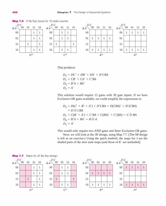
That produces
DD � DC� � DB� � DA� � D�CBA
DC � CB� � CA� � C�BA
DB � B�A � BA�
DA � A�
This solution would require 12 gates with 30 gate inputs. If we haveExclusive-OR gates available, we could simplify the expressions to
DD � D(C� � B� � A�) � D�CBA � D(CBA)� � D�(CBA)
� D � CBA
DC � C(B� � A�) � C�BA � C(BA)� � C�(BA) � C � BA
DB � B�A � BA� � B � A
DA � A�
This would only require two AND gates and three Exclusive-OR gates.Next, we will look at the JK design, using Map 7.7. (The SR design
is left as an exercise.) Using the quick method, the maps for J are theshaded parts of the next state maps (and those of K� are unshaded).
438 Chapter 7 The Design of Sequential Systems
00 01 11 10
00
01
11
10
D CB A
11
1 1
11
11
D★ C★ B★ A★
00 01 11 10
00
01
11
10
D CB A
1 1
11
1 1
1 1
00 01 11 10
00
01
11
10
D CB A
1 1
1111
11
00 01 11 10
00
01
11
10
D CB A
1
1111
111
Map 7.6 D flip flop inputs for 16-state counter.
00 01 11 10
00
01
11
10
D CB A
11
1 1
1
11
D★ C★ B★ A★
00 01 11 10
00
01
11
10
D CB A
1 1
11
1 1
00 01 11 10
00
01
11
10
D CB A
1111
00 01 11 10
00
01
11
10
D CB A
1 1 1
1 111
1111
1111
Map 7.7 Maps for JK flip flop design.
mar91647_c07a_415_465.qxd 11/24/08 12:01 PM Page 438

7.2 The Design of Synchronous Counters 439
This produces the equations
JD � KD � CBA
JC � KC � BA
JB � KB � A
JA � KA � 1
Note that since J = K for each of the flip flops, they are being used as T flip flops (that is, either they remain unchanged or they toggle). Wecould extend the design to 5 flip flops, counting to 31 by adding flip flopE with inputs
JE � KE � DCBA
A circuit to implement this system using JK flip flops is shown inFigure 7.6.
JA 1
Clock
K
JB
K
JC
K
JD
OV
K
Figure 7.6 A 4-bit counter.*
The brown AND gate is not necessary if this is a stand-alone counter; theoutput of the A flip flop would be connected directly to JB and KB. TheOV output is 1 when the counter is in state 15 (1111). OV could be con-nected to the JK inputs of another flip flop or, if we built two 4 flip flopcircuits like the one above, we could connect the OV output of one to theinput where a 1 is now connected to construct an 8-bit counter.
We will next look at an up/down counter, that is, one that can countin either direction, depending upon a control input. We will label thatcontrol input x, such that the counter counts up when x � 0 and downwhen x � 1.† The state table for such a counter is shown as Table 7.9.
*Note that the combinational logic is multilevel. The term CBA is produced by using theoutput of the BA AND gate. In this way, we could extend the counter to any number ofbits by adding as many flip flop/AND gate pairs as are needed.
†In commercial counters, this input is often labeled D�U�, where the notation implies thatdown is active high and up is active low, just as we defined x.
Table 7.9 An up/down counter.
x C B A C� B� A�
0 0 0 0 0 0 10 0 0 1 0 1 00 0 1 0 0 1 10 0 1 1 1 0 00 1 0 0 1 0 10 1 0 1 1 1 00 1 1 0 1 1 10 1 1 1 0 0 01 0 0 0 1 1 11 0 0 1 0 0 01 0 1 0 0 0 11 0 1 1 0 1 01 1 0 0 0 1 11 1 0 1 1 0 01 1 1 0 1 0 11 1 1 1 1 1 0
mar91647_c07a_415_465.qxd 11/24/08 12:01 PM Page 439

The maps for C�, B�, and A� are shown in Map 7.8, with the q � 0section shaded for the quick method with JK flip flops.
440 Chapter 7 The Design of Sequential Systems
00 01 11 10
00
01
11
10
x C
B A
C★ B★ A★
1
1 1
1
11
00 01 11 10
00
01
11
10
x C
B A 00 01 11 10
00
01
11
10
x C
B A
11
1
11
11
1 1 1 1 1
1 1 1 1
1
1
Map 7.8 An up/down counter.
From these maps, we can see that
JA � KA � 1
JB � KB � x�A � xA�
JC � KC � x�BA � xB�A�
Just as in the case of the 4- and 5-bit up counters, this pattern continues,yielding (if we had two more flip flops)
JD � KD � x�CBA � xC�B�A�
JE � KE � x�DCBA � xD�C�B�A�
A block diagram for the 3-bit counter is shown in Figure 7.7.
JA
A�
1
Clock
x
K
JB
B� K
JC
C� K
Figure 7.7 An up/down counter.
mar91647_c07a_415_465.qxd 11/24/08 12:01 PM Page 440

7.2 The Design of Synchronous Counters 441
We will look next at a decimal or decade counter, one that goes through thesequence
0 1 2 3 4 5 6 7 8 9 0 1 . . .
The state (truth) table is similar to that for the binary counter, as seen below
EXAMPLE 7.6
D C B A D� C� B� A�
0 0 0 0 0 0 0 10 0 0 1 0 0 1 00 0 1 0 0 0 1 10 0 1 1 0 1 0 00 1 0 0 0 1 0 10 1 0 1 0 1 1 00 1 1 0 0 1 1 10 1 1 1 1 0 0 01 0 0 0 1 0 0 11 0 0 1 0 0 0 01 0 1 0 X X X X1 0 1 1 X X X X1 1 0 0 X X X X1 1 0 1 X X X X1 1 1 0 X X X X1 1 1 1 X X X X
00 01 11 10
00
01
11
10
D CB A
X
X
X X
XX
1
D* C★ B★ A★
00 01 11 10
00
01
11
10
D CB A
1 X
X
X
X
1
1
00 01 11 10
00
01
11
10
D CB A
11
00 01 11 10
00
01
11
10
D CB A
1 1
1 1
111
11
X
X
X
X X
XX
X
X
X X
XX
X
★
The next state for the 9 (1001) row is 0 (0000) and the remaining nextstates are don’t cares, since states 10 through 15 are never reached. Wehave included rows in this table for the unused states because they areneeded to produce don’t cares on the maps. Some may write the statetable without these rows and then convert it to this truth table (as we did inthe last section). The maps for the next state, with the J section shaded forfinding J and K using the quick method, are shown next.
From this we can see that
JD � CBA KD � A
JC � KC � BA
mar91647_c07a_415_465.qxd 11/24/08 12:01 PM Page 441

JB � D�A KB � A
JA � KA � 1
We will next design a counter that goes through some sequence of statesthat are not in numeric order
0 3 2 4 1 5 7 and repeat
(This is CE9.) Note that the cycle is 7 states; it never goes through state 6.We can now draw the state table (in any order) or go directly to the truthtable, including a row for the unused state.
442 Chapter 7 The Design of Sequential Systems
EXAMPLE 7.7
q1 q2 q3 q1� q2
� q3�
0 0 0 0 1 10 0 1 1 0 10 1 0 1 0 00 1 1 0 1 01 0 0 0 0 11 0 1 1 1 11 1 0 X X X1 1 1 0 0 0
The table can be completed either by going through it row by row and see-ing that state 0 goes to 3, state 1 goes to 5, and so forth, or by following thesequence, first filling in the next state for row 0 as 3, then a next state of 2for state 3, and so forth. In the first approach, when we get to state 6, wefind that it is not in the sequence, and thus the next state is don’t cares. Inthe second approach, when we get to state 7, we must be sure to enter thenext state as 0. Then, when we get done with the cycle, we find that row 6is empty and also put in don’t cares. We surely write the truth table innumeric order.
The table is repeated below with columns for inputs to SR and T flipflops; we will use the quick method for JK flip flops.
q1 q2 q3 q1� q2
� q3� S1 R1 S2 R2 S3 R3 T1 T2 T3
0 0 0 0 1 1 0 X 1 0 1 0 0 1 10 0 1 1 0 1 1 0 0 X X 0 1 0 00 1 0 1 0 0 1 0 0 1 0 X 1 1 00 1 1 0 1 0 0 X X 0 0 1 0 0 11 0 0 0 0 1 0 1 0 X 1 0 1 0 11 0 1 1 1 1 X 0 1 0 X 0 0 1 01 1 0 X X X X X X X X X X X X1 1 1 0 0 0 0 1 0 1 0 1 1 1 1
For D flip flops, we just use the q1�, q2
�, and q3� columns, producing the
following maps and equations.
mar91647_c07a_415_465.qxd 11/24/08 12:01 PM Page 442
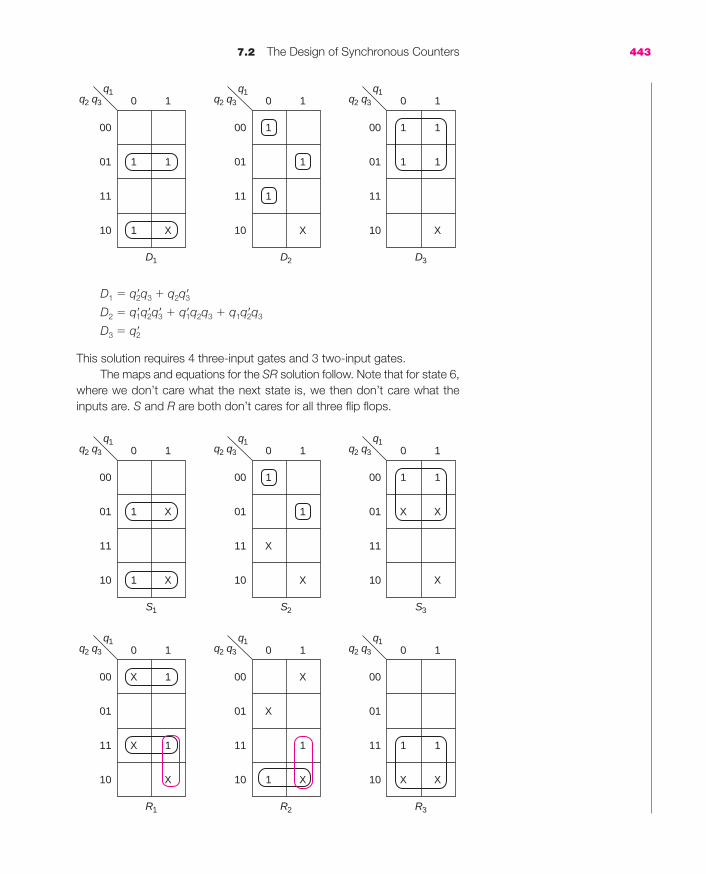
7.2 The Design of Synchronous Counters 443
D1 � q�2q3 � q2q�3
D2 � q�1q�2q�3 � q�1q2q3 � q1q�2q3
D3 � q�2
This solution requires 4 three-input gates and 3 two-input gates.The maps and equations for the SR solution follow. Note that for state 6,
where we don’t care what the next state is, we then don’t care what theinputs are. S and R are both don’t cares for all three flip flops.
0 1q1
q2 q3
X
1 1
1
00
01
11
10
D1
0 1q1
q2 q3
X
1
1
1
00
01
11
10
D2
0 1q1
q2 q3
X
1
1
1
100
01
11
10
D3
0 1q1
q2 q3
X
1 X
1
00
01
11
10
S1
0 1q1
q2 q3
X
X
X X
1
1
00
01
11
10
S2
0 1q1
q2 q3
X
1 100
01
11
10
S3
0 1q1
q2 q3
X
1
1
1
00
01
11
10
R1
0 1q1
q2 q3
X
XX
X
X
00
01
11
10
R2
0 1q1
q2 q3
XX
111
00
01
11
10
R3
mar91647_c07a_415_465.qxd 11/24/08 12:01 PM Page 443

S1 � q2�q3 � q2q3� R1 � q2�q3� � q2q3 � S1�
� q2�q3� � q1q2
S2 � q1�q2�q3� � q1q2�q3 R2 � q1q2 � q2q3�
S3 � q2� R3 � q2
Even taking advantage of the sharing or using a NOT for R1, this requiresmore logic than the D solution (10 or 11 gates).
We will compute the T solution; the maps and the equations are shownnext.
444 Chapter 7 The Design of Sequential Systems
0 1q1
q2 q3
X
1
1
1
1
00
01
11
10
T1
0 1q1
q2 q3
X
1
1
1
1
00
01
11
10
T2
0 1q1
q2 q3
X
1
1 1
100
01
11
10
T3
T1 � q�1q�2q3 � q2q�3 � q1q2 � q1q�3
T2 � q�1q�3 � q1q3
T3 � q�2q�3 � q2q3
This solution requires 11 gates.Finally, we will solve this system using the quick method for JK flip flops
as shown on the maps and equations below.
0 1q1
q2 q3
X
1
00
01
11
10
0 1q1
q2 q3
X
1
00
01
11
10
0 1q1
q2 q3
11
00
01
11
10
1
1
1
1
1 1
X
q1★ q2
★ q3★
J1 � q�2q3 � q2q�3 K1 � q�3 � q2
J2 � q�1q�3 � q1q3 K2 � q1 � q�3
J3 � q�2 K3 � q2
mar91647_c07a_415_465.qxd 11/24/08 12:01 PM Page 444

7.2 The Design of Synchronous Counters 445
This solution requires 8 two-input gates, although the gate for K1 could bereplaced by a NOT gate and the gate for K2 could be eliminated, since bychoosing the don’t cares as 1’s in both places, we get
K1 � J�1 and K2 � J2
If we do not have a static clear (or do not use it) and turn the systemon, we do not know in what state each flip flop will be initially. If wecare, we should clear the flip flops or use some combination of clears andpresets to get the system into the proper initial state. Often, all we careabout is that once this is turned on, it goes through the desired sequenceafter one or two clocks. That will always happen if it is initialized to oneof the states in the sequence. But, if it is initialized to one of the unusedstates, it is not obvious what will happen. When we designed the systemsof the last two examples, we assumed that that state never happened andthus made the next state a don’t care.
Once we complete the design, there are no longer any don’t cares.The algebraic expressions (or the block diagrams) specify what happensfor all possible combinations of variables.
We can determine what would happen by assuming we are in state 110.Thus, we would make q1 � 1, q2 � 1, and q3 � 0 in the equations. For Dflip flops, we would get
D1 � q2�q3 � q2q�3 � 00 � 11 � 1
D2 � q1�q2�q�3 � q1�q2q3 � q1q2�q3 � 001 � 011 � 100 � 0
D3 � q2� � 0
In that case, the system would go to state 4 (100) on the first clock and con-tinue through the sequence from there. (With the design shown, we wouldalso go to state 4 with SR flip flops, to state 2 with T flip flops, and to state 0with JK flip flops.)
If this were not satisfactory, we could go back and redesign the systemby replacing the don’t cares in row 110 of the truth table by the desired nextstate.
A state diagram, showing the behavior of the system designed with Dor SR flip flops, including what happens if the system starts in the unusedstate, is shown next.
EXAMPLE 7.7 (Cont.)
1
7
0
5
4
3
2
6
mar91647_c07a_415_465.qxd 11/24/08 12:01 PM Page 445

Note that there are no labels on the paths, since there is no input to the sys-tem, and the output is just equal to the state. (It is a Moore system.)
As a final example in this section, we will consider the design of a 2-bitup/down, cycling/saturating counter. This counter has two flip flops, A andB, and thus only four states. It has two control inputs, x and y. If x � 0, itcounts up and if x � 1, it counts down. If y � 0, it cycles, that is, goes 0 1 2 3 0 1 . . . or 3 2 1 0 3 2 . . . , and if y � 1, it saturates, that is, itgoes 0 1 2 3 3 3 . . . or 3 2 1 0 0 0 . . . . (This is a two-flip flop versionof CE10.) The state table for this counter is
446 Chapter 7 The Design of Sequential Systems
EXAMPLE 7.8
A� B�
A B xy � 00 xy � 01 xy � 10 xy � 11
0 0 0 1 0 1 1 1 0 00 1 1 0 1 0 0 0 0 01 0 1 1 1 1 0 1 0 11 1 0 0 1 1 1 0 1 0
Since this is a problem with two inputs, there are four input combinationsand thus four columns in the next state section. (If this were a Mealy system,there would also be four output columns.) This can easily be converted intoa 16-row truth table or directly to maps. The latter is easiest if we are toimplement this with either D or JK flip flops. In going to the maps, care mustbe taken since both the rows and columns are in binary order, not maporder. The maps for DA (A�) and DB (B�) are shown below.
The functions are rather complex.
DA � x�A�B � x�AB� � x�yA � xAB � xy�A�B�
DB � x�yA � AB� � x�B� � y�B�
� x�yA � AB� � x�B� � xy�A�B�
00 01 11 10
00
01
11
10
x y
A B
1
00 01 11 10
00
01
11
10
x y
A B
1
111
11
11
1 1
111
1
1
A B★ ★
mar91647_c07a_415_465.qxd 11/24/08 12:01 PM Page 446

7.3 Design of Asynchronous Counters 447
Even if we were to implement this counter with JK flip flops, there isa great deal of combinational logic, as can be seen from the maps andequations below.
JA � x�B � xy�B� KA � xB� � x�y�B
JB � x� � y� � A KB � x � y� � A�
7.3 DESIGN OF ASYNCHRONOUSCOUNTERS
Binary counters are sometimes designed without a clock input. They areconstructed from the same clocked flip flops (typically JK) as syn-chronous counters, but each flip flop is triggered by the transition of theprevious one. Consider the circuit of Figure 7.8 with two flip flops.
00 01 11 10
00
01
11
10
x y
A B 00 01 11 10
00
01
11
10
x y
A B
111
11
1
1
11
1
1 1
111
1
A B★ ★
[SP 5, 6, 7; EX 5, 6, 7, 8, 9, 10, 11; LAB]
B
K
1
1J A
K
Count
J
Figure 7.8 A 2-bit asynchronous counter.
When the Count signal goes from 1 to 0, flip flop A is triggered. If itstarted out at 0, it goes to 1. The 0 to 1 transition on the output of A, andthus on the clock input of B, has no effect. When the next negative tran-sition on Count occurs, A will go from 1 to 0 causing the clock input toB to do the same. Since J and K are 1, flip flop B will change states. Sincethere is a delay from the clock edge to the output change, flip flop B isclocked somewhat later than A and thus its output changes later. This isemphasized in the timing diagram of Figure 7.9. We assume in thisdiagram that flip flops A and B both start at 0.
mar91647_c07a_415_465.qxd 11/24/08 12:01 PM Page 447

448 Chapter 7 The Design of Sequential Systems
There are two things that are different about this timing diagram from theprevious ones. Since the Count signal is not necessarily a clock, it mightbe rather irregular.* Second, the first flip flop (A) changes shortly afterthe negative edge of the Count (the dashed line), but the second flip flop(B) does not change until somewhat after A changes, and thus the delayfrom the clock is much greater. This becomes more significant as thechanges ripple through several flip flops.
Note that the flip flops (BA) go through the sequence 00, 01, 10, 11,and repeat. Thus, this is a 2-bit counter. We can obtain a 4-bit counter byconnecting four flip flops in the same fashion. A block diagram is shownin Figure 7.10.
The timing is shown in Figure 7.11, where there is one unit of delaythrough each flip flop and the clock period is 10 units.
Count
A
B
Figure 7.9 Timing delay in an asynchronous counter.
B
K
1
1J A
K
Count
JC
K
1
JD
K
1
J
Figure 7.10 A 4-bit asynchronous counter.
*The Clock input for synchronous counters is really a Count input also. Although the clockis usually regular, it need not be. The counter will change states on each negative transition.
0
Count
A
B
C
D
100
Figure 7.11 Timing for the 4-bit counter.
mar91647_c07a_415_465.qxd 11/24/08 12:01 PM Page 448

7.3 Design of Asynchronous Counters 449
Notice that A changes one unit of time after the trailing edge of the clock,B one unit after a trailing edge of A, C after B, and D after C. Thus, thechange in D occurs 4 units after the clock (almost at the next leadingedge in this example).
Notice also that this counter does go through the sequence 0 1 2 34 5 6 7 8 9 10 (as far as the timing diagram goes) and would continuethrough 11 12 13 14 15 0 . . . .
The advantage of the asynchronous counter is the simplicity of thehardware. There is no combinational logic required. The disadvantage isspeed. The state of the system is not established until all of the flip flopshave completed their transition, which, in this case, is four flip flopdelays. If the counter were larger or the clock faster, it might not reachits final state until after the next negative clock transition. In that case,its value would not be available for other parts of the system at the nextclock. Also, care must be taken when using outputs from this countersince it goes through unintended states. For example, a close inspectionof the timing diagram as the counter moves from state 7 to state 8, theshaded area in Figure 7.11, shows that it is in state 6, state 4, and thenstate 0 before flip flop D goes to 1 and it reaches state 8. These shortperiods are not important if the outputs are used to light a display or asthe inputs to a clocked flip flop, but they could produce spikes thatwould trigger a flip flop if used as a clock or Count input.
Design an asynchronous base-12 counter using JK flip flops with active lowclears and NAND gates.
The easiest way to do this is to take the 4-bit binary counter and resetit when it reaches 12. Thus, the circuit below computes (DC)� and uses thatto reset the counter.
EXAMPLE 7.9
JD
CLR� K
JC
CLR� K
JB
CLR� K
J 1
Clock
A
CLR� K
As can be seen from the timing diagram below, the counter cycles
0 1 2 3 4 5 6 7 8 9 10 11 (12) 0
mar91647_c07a_415_465.qxd 11/24/08 12:01 PM Page 449
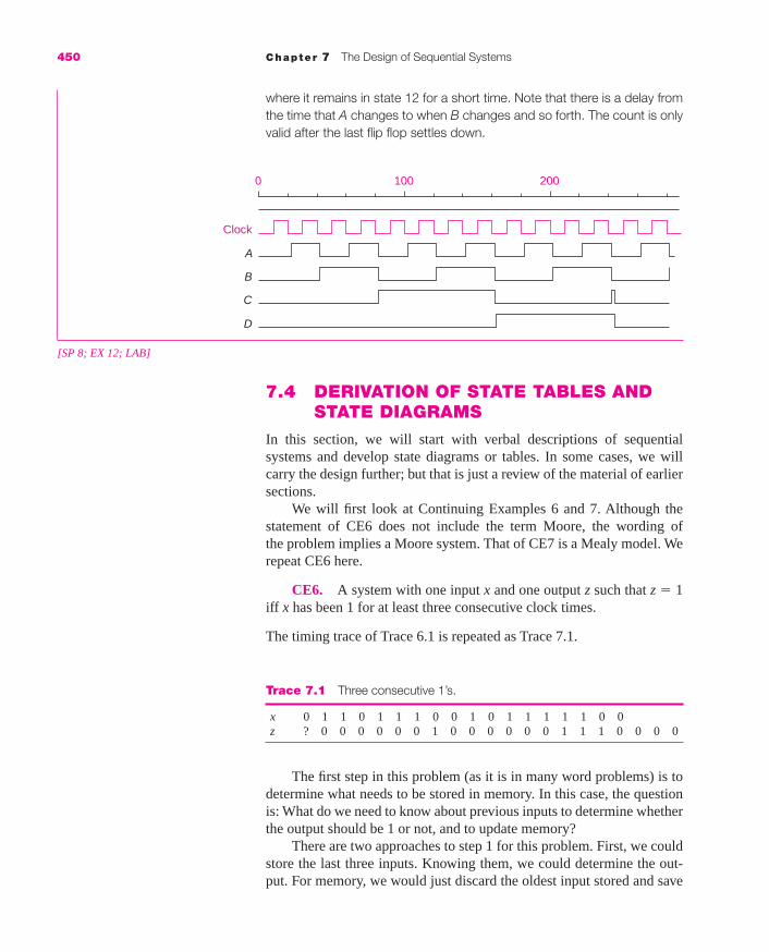
where it remains in state 12 for a short time. Note that there is a delay fromthe time that A changes to when B changes and so forth. The count is onlyvalid after the last flip flop settles down.
450 Chapter 7 The Design of Sequential Systems
0
A
100 200
Clock
B
C
D
[SP 8; EX 12; LAB]
7.4 DERIVATION OF STATE TABLES ANDSTATE DIAGRAMS
In this section, we will start with verbal descriptions of sequentialsystems and develop state diagrams or tables. In some cases, we willcarry the design further; but that is just a review of the material of earliersections.
We will first look at Continuing Examples 6 and 7. Although thestatement of CE6 does not include the term Moore, the wording ofthe problem implies a Moore system. That of CE7 is a Mealy model. Werepeat CE6 here.
CE6. A system with one input x and one output z such that z � 1iff x has been 1 for at least three consecutive clock times.
The timing trace of Trace 6.1 is repeated as Trace 7.1.
Trace 7.1 Three consecutive 1’s.
x 0 1 1 0 1 1 1 0 0 1 0 1 1 1 1 1 0 0z ? 0 0 0 0 0 0 1 0 0 0 0 0 0 1 1 1 0 0 0 0
The first step in this problem (as it is in many word problems) is todetermine what needs to be stored in memory. In this case, the questionis: What do we need to know about previous inputs to determine whetherthe output should be 1 or not, and to update memory?
There are two approaches to step 1 for this problem. First, we couldstore the last three inputs. Knowing them, we could determine the out-put. For memory, we would just discard the oldest input stored and save
mar91647_c07a_415_465.qxd 11/24/08 12:01 PM Page 450

7.4 Derivation of State Tables and State Diagrams 451
the last two plus the present one. The inputs are already coded in binary(step 2). If we store the oldest input in q1, the next oldest in q2, and themost recent one in q3, we get the state table of Table 7.10.
The new value of q3, q3� � x; it will hold the most recent input.
Similarly, q2� � q3 and q1
� � q2. The output is only 1 when the system isin state 111.
For the second approach, we store in memory the number of con-secutive 1’s, as follows:*
A none, that is, the last input was 0
B one
C two
D three or more
That, too, is sufficient information, since the output is 1 if and only ifthere have been three or more.
The state diagram and the state table are the same as those in Figure 7.1and are repeated here as Figure 7.12.
*We will just name the memory contents, that is, the state with letters A, B, C, . . . anddeal with coding these into binary later.
Figure 7.12 State diagram and state table.
1
no 1’s
two 1’s three ormore 1’s
00 0
11
one 1
B0
C0
0
A0
D1
1
q�
q x � 0 x � 1 z
A A B 0B A C 0C A D 0D A D 1
This approach required only four states, whereas the first approachrequired eight. The first approach uses three flip flops, whereas the sec-ond uses only two. This is not much of a difference. Consider, however,what happens if the problem required a 1 output iff the input has been 1for 25 or more consecutive clock times. For the first approach, we wouldneed to save the last 25 inputs, using 25 flip flops. The state table wouldhave 225 rows. The second approach requires 26 states (no 1’s through 25or more 1’s). They could be coded with just five flip flops.
The next step in the process is to reduce the state table, if possible,to one with fewer states. Although we will not be prepared to considerthis step until Chapter 9, it is clear that Table 7.10 has some redundantstates. For example, both states 000 and 100 go to state 000 if the inputis 0; they go to state 001 if the input is 1; both have the same output.
Table 7.10 Three flip flop statetable.
q1� q2
� q3�
q1 q2 q3 x � 0 x � 1 z
0 0 0 0 0 0 0 0 1 00 0 1 0 1 0 0 1 1 00 1 0 1 0 0 1 0 1 00 1 1 1 1 0 1 1 1 01 0 0 0 0 0 0 0 1 01 0 1 0 1 0 0 1 1 01 1 0 1 0 0 1 0 1 01 1 1 1 1 0 1 1 1 1
mar91647_c07a_415_465.qxd 11/26/08 12:19 PM Page 451
Thus, only one of them is needed. Indeed, this table can be reduced toone with only four states. The state table obtained using the secondapproach cannot be reduced.
Even if we do not reduce the table, we can proceed to choose a stateassignment (whether we take advantage of the techniques in Chapter 9 tochoose a “good” assignment or just pick any convenient one) and thencomplete the design. The system might be more expensive than one wewould have obtained, but it will still work correctly.
For the first design, the state assignment has already been made. Welabeled the flip flops q1, q2, and q3. The flip flop inputs require no logicfor D flip flops.
D1 � q2 D2 � q3 D3 � x
For JK flip flops,
J1 � q2 J2 � q3 J3 � x
K1 � q2� K2 � q3� K3 � x�
A NOT gate is needed for x� if we use JK flip flops. For either type of flipflop, one AND gate is needed for z:
z � q1 q2 q3
For the second approach, we have already constructed the designtruth table for one state assignment in Table 7.2 and found that
D1 � q1� � xq2 � xq1 or J1 � xq2 K1 � x
D2 � q2� � xq2� � xq1 or J2 � x K2 � x� � q1
z � q1q2
The corresponding Mealy example is CE7.
CE7. A system with one input x and one output z such that z � 1 at a clock time iff x is currently 1 and was also 1 at the previoustwo clock times.
Another way of wording this same problem is
CE7#. A Mealy system with one input x and one output z such thatz � 1 iff x has been 1 for three consecutive clock times.
The timing trace corresponding to this problem is shown in Trace 7.2.
452 Chapter 7 The Design of Sequential Systems
Trace 7.2 Timing trace for CE7.
x 0 1 1 0 1 1 1 0 0 1 0 1 1 1 1 1 0 0z 0 0 0 0 0 0 1 0 0 0 0 0 0 1 1 1 0 0 0 0
There are two approaches for this problem, as well. We need onlystore the last two inputs (rather than three for the Moore model). Thisproduces the state table of Table 7.11.
mar91647_c07a_415_465.qxd 11/24/08 12:01 PM Page 452

7.4 Derivation of State Tables and State Diagrams 453
For the second approach, we store in memory the number of con-secutive 1’s, as follows:
A none, that is, the last input was 0
B one
C two or more
That, too, is sufficient information since the output is 1 if and only ifthere were previously two or more 1’s and the present input is a 1. If thepresent input is a 0, the next state is A; otherwise, we move from A to Band from B to C. The state diagram is shown in Figure 7.13.
The description can also be written as a state table, as shown inTable 7.12.
0/0
0/0two or more 1’s
one 1
no 1’s
1/1
0/0
1/0
1/0B
A
C
Figure 7.13 State diagram for threeconsecutive 1’s.
Table 7.12 State table for threeconsecutive 1’s.
q� zq x � 0 x � 1 x � 0 x � 1
A A B 0 0B A C 0 0C A C 0 1
Table 7.11 State table for saving last twoinputs.
q1� q2
� zq1 q2 x � 0 x � 1 x � 0 x � 1
0 0 0 0 0 1 0 00 1 1 0 1 1 0 01 0 0 0 0 1 0 01 1 1 0 1 1 0 1
mar91647_c07a_415_465.qxd 11/24/08 12:01 PM Page 453

To compare the behavior of the Mealy and Moore models, we willlook at the timing diagram for each (using the four-state Moore modeland the three-state Mealy model).
454 Chapter 7 The Design of Sequential Systems
Clock
x
q
z
z
Mealy
A B C C C C C C A B C A B C C A B
A BADCBACBADDDDDCBq
Moore
*Notice that, in this example, we can determine the output for two or three clocks after theinput is no longer known, since even if both inputs were 1, the output would remain 0 atleast until the clock time after the one shown.
EXAMPLE 7.10
Basically, the Moore model output is the same as the Mealy, but delayedby one clock period. It does not have any false outputs, since z dependsonly on the flip flops, all of which change at the same time.
Design both a Moore and a Mealy system with one input x and one out-put z such that z � 1 iff x has been 1 for exactly three consecutive clocktimes.
A sample input/output trace for such a system is
x 0 1 1 1 1 1 1 1 0 1 1 0 1 1 1 0 1
z-Mealy 0 0 0 0 0 0 0 0 0 0 0 0 0 0 0 1 0 0 0*
z-Moore 0 0 0 0 0 0 0 0 0 0 0 0 0 0 0 0 1 0 0 0
↑ ↑
We cannot tell whether there should be a 1 output when the third consecu-tive 1 input occurs. The past history and the present input are the same atthe two places indicated with arrows. It is not until the next input arrives thatwe know that there have been exactly three 1’s in a row. For the Mealymodel we now need five states,
A none, that is, the last input was 0
B one 1 in a row
C two 1’s in a row
D three 1’s in a row
E too many (more than 3) 1’s in a row
mar91647_c07a_415_465.qxd 11/24/08 12:01 PM Page 454

7.4 Derivation of State Tables and State Diagrams 455
The state diagram begins like that of the previous solution. However,when we get a third 1 input, we go to state D. From D, a 0 input producesa 1 output; a 1 input gets us to a new state, E. Sometimes, we think of state Aas nowhere, that is, we are looking for the first 1 to get started on the suc-cessful path to a 1 output. In that case, state E is worse than nowhere,since we must first get a 0 before we can even begin to look for three 1’s.The complete state diagram is shown next.
The implementation of this system requires three flip flops. The design is leftas an exercise.
For the Moore model, we need a state D to indicate exactly three 1’s.From there, it goes to E on another 1, indicating too many 1’s. State F isreached on a 0 input; it is the state with a 1 output. The state table is shownbelow. (We could have constructed a state diagram for this version or astate table for the Mealy model.)
0/0
0/0more than three 1’s
one 1
no 1’s
1/0
1/01/0
1/0
three 1’s
0/0
1/0
0/1
A
B E
C D
two 1’s
q�
q x � 0 x � 1 z
A A B 0B A C 0C A D 0D F E 0E A E 0F A B 1
Design a Mealy system whose output is 1 iff the input has been 1 for threeconsecutive clocks, but inputs are nonoverlapping. (That means that a 1input can only be used toward one 1 output.)
EXAMPLE 7.11
mar91647_c07a_415_465.qxd 11/24/08 12:01 PM Page 455
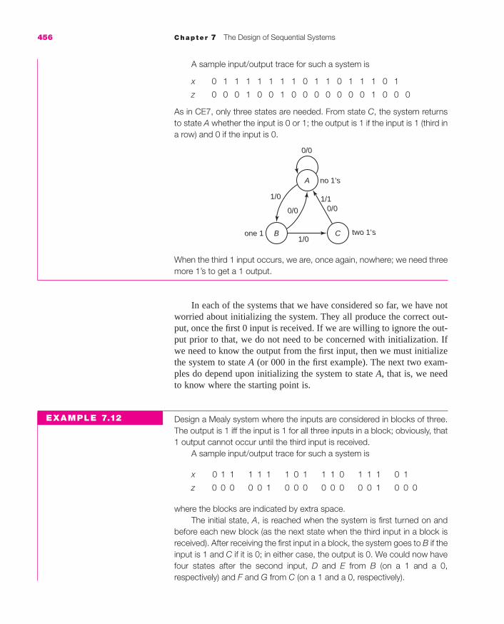
A sample input/output trace for such a system is
x 0 1 1 1 1 1 1 1 0 1 1 0 1 1 1 0 1
z 0 0 0 1 0 0 1 0 0 0 0 0 0 0 1 0 0 0
As in CE7, only three states are needed. From state C, the system returnsto state A whether the input is 0 or 1; the output is 1 if the input is 1 (third ina row) and 0 if the input is 0.
When the third 1 input occurs, we are, once again, nowhere; we need threemore 1’s to get a 1 output.
In each of the systems that we have considered so far, we have notworried about initializing the system. They all produce the correct out-put, once the first 0 input is received. If we are willing to ignore the out-put prior to that, we do not need to be concerned with initialization. Ifwe need to know the output from the first input, then we must initializethe system to state A (or 000 in the first example). The next two exam-ples do depend upon initializing the system to state A, that is, we needto know where the starting point is.
Design a Mealy system where the inputs are considered in blocks of three.The output is 1 iff the input is 1 for all three inputs in a block; obviously, that1 output cannot occur until the third input is received.
A sample input/output trace for such a system is
x 0 1 1 1 1 1 1 0 1 1 1 0 1 1 1 0 1
z 0 0 0 0 0 1 0 0 0 0 0 0 0 0 1 0 0 0
where the blocks are indicated by extra space.The initial state, A, is reached when the system is first turned on and
before each new block (as the next state when the third input in a block isreceived). After receiving the first input in a block, the system goes to B if theinput is 1 and C if it is 0; in either case, the output is 0. We could now havefour states after the second input, D and E from B (on a 1 and a 0,respectively) and F and G from C (on a 1 and a 0, respectively).
0/0
1/1 0/0
two 1’sone 1
no 1’s
0/0
1/0
1/0B
A
C
456 Chapter 7 The Design of Sequential Systems
EXAMPLE 7.12
mar91647_c07a_415_465.qxd 11/24/08 12:01 PM Page 456
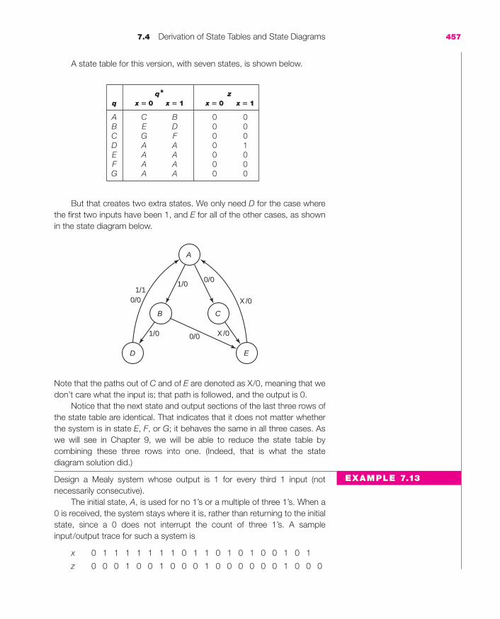
7.4 Derivation of State Tables and State Diagrams 457
But that creates two extra states. We only need D for the case wherethe first two inputs have been 1, and E for all of the other cases, as shownin the state diagram below.
Note that the paths out of C and of E are denoted as X/0, meaning that wedon’t care what the input is; that path is followed, and the output is 0.
Notice that the next state and output sections of the last three rows ofthe state table are identical. That indicates that it does not matter whetherthe system is in state E, F, or G; it behaves the same in all three cases. Aswe will see in Chapter 9, we will be able to reduce the state table bycombining these three rows into one. (Indeed, that is what the statediagram solution did.)
Design a Mealy system whose output is 1 for every third 1 input (notnecessarily consecutive).
The initial state, A, is used for no 1’s or a multiple of three 1’s. When a0 is received, the system stays where it is, rather than returning to the initialstate, since a 0 does not interrupt the count of three 1’s. A sampleinput/output trace for such a system is
x 0 1 1 1 1 1 1 1 0 1 1 0 1 0 1 0 0 1 0 1
z 0 0 0 1 0 0 1 0 0 0 1 0 0 0 0 0 0 1 0 0 0
A
1/0 0/0
0/01/0 X/0
X/01/1
0/0
CB
ED
EXAMPLE 7.13
q� zq x � 0 x � 1 x � 0 x � 1
A C B 0 0B E D 0 0C G F 0 0D A A 0 1E A A 0 0F A A 0 0G A A 0 0
A state table for this version, with seven states, is shown below.
mar91647_c07a_415_465.qxd 11/24/08 12:01 PM Page 457

The state diagram is thus
CE8. Design a Moore system whose output is 1 iff three consecutive 0inputs occurred more recently than three consecutive 1 inputs.* A sampleinput/output trace for such a system is
x 1 1 1 0 0 1 0 1 1 1 0 0 1 0 0 0 0 1 1 1 1 0 1
z ? ? ? 0 0 0 0 0 0 0 0 0 0 0 0 0 1 1 1 1 0 0 0 0 0
We showed the first three outputs as unknown, assuming that we startedlooking at some time when the system was running or that we turned it onand did not know what state it came up in. The wording implies that whenfirst turned on, the system should have a 0 output, since there have notrecently been three consecutive 1’s. (This is the same example that we didat the end of Section 7.1.)
We will call the initial state S1. The first path to develop is to get the out-put to change from 0 to 1. That part of the state diagram is shown below.
S1
0
S2
0
S4
1
0
0
0
S3
0
0/0
1/1
two 1’s
0/0 0/0
no 1’s
one 1
1/0
1/0B
A
C
458 Chapter 7 The Design of Sequential Systems
*We are assuming that three means three or more, not exactly three.
EXAMPLE 7.14
mar91647_c07a_415_465.qxd 11/24/08 12:01 PM Page 458
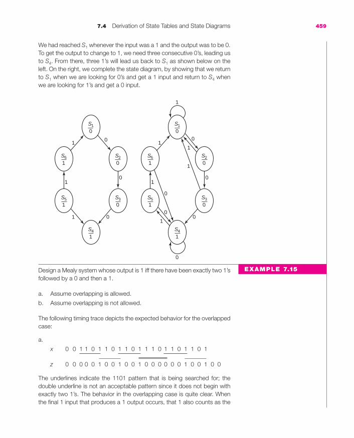
We had reached S1 whenever the input was a 1 and the output was to be 0.To get the output to change to 1, we need three consecutive 0’s, leading usto S4. From there, three 1’s will lead us back to S1 as shown below on theleft. On the right, we complete the state diagram, by showing that we returnto S1 when we are looking for 0’s and get a 1 input and return to S4 whenwe are looking for 1’s and get a 0 input.
Design a Mealy system whose output is 1 iff there have been exactly two 1’sfollowed by a 0 and then a 1.
a. Assume overlapping is allowed.
b. Assume overlapping is not allowed.
The following timing trace depicts the expected behavior for the overlappedcase:
a.
x 0 0 1 1 0 1 1 0 1 1 0 1 1 1 0 1 1 0 1 1 0 1
z 0 0 0 0 0 1 0 0 1 0 0 1 0 0 0 0 0 0 1 0 0 1 0 0
The underlines indicate the 1101 pattern that is being searched for; thedouble underline is not an acceptable pattern since it does not begin withexactly two 1’s. The behavior in the overlapping case is quite clear. Whenthe final 1 input that produces a 1 output occurs, that 1 also counts as the
S1
0
S2
0
S4
1
1
1
0
0
0
S3
0
S6
1
1
S5
1
1
0
S1
0
S2
0
S4
1
11
0
0
0
1
0
0
S3
0
S6
1
1
S5
1
1
7.4 Derivation of State Tables and State Diagrams 459
EXAMPLE 7.15
mar91647_c07a_415_465.qxd 11/24/08 12:01 PM Page 459

first of two consecutive 1 inputs for the next 1 output. The two brownunderlines indicate overlapping patterns.
It is often easiest to begin the state diagram by following a successpath, that is, one leading to the desired output, as shown below.
State A is the nowhere state, where we are looking for the first 1. Onsuccessive 1’s, we move to B and C; a 0 takes us to D and then a 1 pro-duces the 1 output. Since overlapping is allowed, that 1 is the first 1toward a new sequence, and we return to state B from D. We must alsocomplete the failed paths. A 0 in any state other than C (where we arelooking for a 0) returns us to state A. If, after getting two consecutive 1’s,we get a third, we need another state, E, which indicates that we have toomany 1’s and are waiting for a 0 before we can go back to state A andstart again. The complete state diagram for the overlapped solution is thusshown below.
1/0
1/0
1/01/1
0/0
0/0
0/0
1/0
0/0
0110
two 1’smore than two 1’s
0/0
one 1
nowhere, lastinput � 0
A
B
C E
D
1/0
1/0
0/00110
1/1
one 1
two 1's
nowhere, lastinput � 0
C D
0/0
A
B
460 Chapter 7 The Design of Sequential Systems
mar91647_c07a_415_465.qxd 11/24/08 12:01 PM Page 460

7.4 Derivation of State Tables and State Diagrams 461
There are two interpretations to consider in the nonoverlappingcase. The first is shown as b-1. In that case, when a 1 output occurs,there must be a 0 input before we can have exactly two 1’s. Thus, after thefirst 1 output, we do not get started toward another 1 output until after a0 input.
x 0 0 1 1 0 1 1 0 1 1 0 1 1 1 0 1 1 0 1 1 0 1
b-1 0 0 0 0 0 1 0 0 0 0 0 1 0 0 0 0 0 0 1 0 0 0 0 0
A second interpretation (perhaps a little far-fetched) is that once we havecompleted a pattern, we need exactly two more 1’s followed by a 10; thatis what accepts the double-underlined sequence.
x 0 0 1 1 0 1 1 0 1 1 0 1 1 1 0 1 1 0 1 1 0 1
b-2 0 0 0 0 0 1 0 0 0 0 0 1 0 0 0 1 0 0 0 0 0 1 0 0 0
The two solutions for the nonoverlapping versions are shown next. Theybegin exactly like the overlapping version but behave differently when weget the input that produces a 1 output.
b-21/0
1/0
1/0
0/01/1
0/0
1/0
0/0
0110
two 1’s
0/0
one 1
nowhere, lastinput � 0
A
B
C E
D
0/0
b-11/0
1/0
1/0
0/0
0/0
1/0
0/01/1
0110
two 1’s
0/0
one 1
nowhere, lastinput � 0
A
B
C E
D
0/0
EXAMPLE 7.16Finally, we will look at the design of the bus controller CE11.
CE11. Design a Moore model bus controller that receives requests on sep-arate lines, R0 to R3, from four devices desiring to use the bus. It has fouroutputs, G0 to G3, only one of which is 1, indicating which device is grantedcontrol of the bus for that clock period. The low number device has the
mar91647_c07a_415_465.qxd 11/24/08 12:01 PM Page 461

highest priority, if more than one device requests the bus at the same time.We look at both interrupting controllers (where a high priority device canpreempt the bus) and one where a device keeps control of the bus once itgets it until it no longer needs it.
The bus controller has five states:
A: idle, no device is using the bus
B: device 0 is using the bus
C: device 1 is using the bus
D: device 2 is using the bus
E: device 3 is using the bus
We will first consider the case where once device j gets control of the bus(Gj � 1), it retains that control until it is no longer requesting it (until Rj � 0).Further, we will assume that it must return to the idle state for one clockperiod between allocations. This results in the following state diagram.
462 Chapter 7 The Design of Sequential Systems
A0000
0000
1XXX
1XXX X1XX XX1X XXX1
01XX
0XXX
001X XX0X
XXX0
X0XX 0001
C0100
B1000
D0010
E0001
The system remains in the idle state if there are no requests. It goes tothe highest priority state when there are one or more requests. Thus, itgoes to state B if R0 = 1, no matter what the other R’s are. Once it hasgranted the bus, it remains in that state if that device is still requesting thebus and returns to the idle state otherwise. If there is another requestpending, it is idle for one clock period before granting the next highestpriority request.
mar91647_c07a_415_465.qxd 11/24/08 12:01 PM Page 462

7.4 Derivation of State Tables and State Diagrams 463
If the idle period is not necessary, the state diagram becomes muchmore complex. When any device no longer needs the bus, the controller willreturn to state A if no other device is requesting it; but it proceeds directly togranting the highest priority request. A state table for such a system isshown below.
q q� G0 G1 G2 G3
R0 0 0 0 0 0 0 0 0 1 1 1 1 1 1 1 1R1 0 0 0 0 1 1 1 1 0 0 0 0 1 1 1 1R2 0 0 1 1 0 0 1 1 0 0 1 1 0 0 1 1R3 0 1 0 1 0 1 0 1 0 1 0 1 0 1 0 1
A A E D D C C C C B B B B B B B B 0 0 0 0B A E D D C C C C B B B B B B B B 1 0 0 0C A E D D C C C C B B B B C C C C 0 1 0 0D A E D D C C D D B B D D B B D D 0 0 1 0E A E D E C E C E B E B E B E B E 0 0 0 1
Note that in this version, we can go from any state to any other state. Therewould be 20 paths on the state diagram. The partial diagram below showsjust the paths to and from state C.
Finally, we will look at a preemptive controller, where a high prioritydevice will take control from a lower priority one, even if the lower priorityone is still using the bus. For this case (whether we must return to state 0 ornot), we remain in states C, D, and E only if that device is requesting the busand no higher priority device is simultaneously requesting it. The state
X1XX
01XX
01XX
10XX
C0100
B1000
A0000
000001X0
0001
01XX
001X
E0001
D0010
mar91647_c07a_415_465.qxd 11/24/08 12:01 PM Page 463

Although the state diagram for this version would require the same 20 pathsas was needed for the second version, the logic is much simpler. Thecondition for going to state B, from each state is 1XXX (R1), to C is 01XX(R1�R2), to D is 001X (R1�R2�R3), and to E is 0001 (R1�R2�R3�R4) (the same as thecondition from state A in all of the versions).
464 Chapter 7 The Design of Sequential Systems
[SP 9; EX 13, 14, 15, 16, 17]
A0000
0000
1XXX
1XXX 01XX 001X
000101XX
0XXX
001X
0001
XXX01XXXX1XXXX1X
XX0X1XXXX1XXX0XX
1XXX
C0100
B1000
D0010
E0001
q q� G0 G1 G2 G3
R0 0 0 0 0 0 0 0 0 1 1 1 1 1 1 1 1R1 0 0 0 0 1 1 1 1 0 0 0 0 1 1 1 1R2 0 0 1 1 0 0 1 1 0 0 1 1 0 0 1 1R3 0 1 0 1 0 1 0 1 0 1 0 1 0 1 0 1
A A E D D C C C C B B B B B B B B 0 0 0 0B A E D D C C C C B B B B B B B B 1 0 0 0C A E D D C C C C B B B B B B B B 0 1 0 0D A E D D C C C C B B B B B B B B 0 0 1 0E A E D D C C C C B B B B B B B B 0 0 0 1
diagram for the system that must return to idle for one clock period isshown first and then the state table for the system that can go directly to thenext state having use of the bus.
mar91647_c07a_415_465.qxd 11/24/08 12:01 PM Page 464

7.5 Solved Problems 465
We will first construct a truth table and map the functions.
7.5 SOLVED PROBLEMS
1. For the following state table and state assignment, showequations for the next state and the output.
qq� z
x � 0 x � 1 x � 0 x � 1
A C A 1 0B B A 0 1C B C 1 0
q q1 q2
A 0 1B 1 1C 0 0
q x q1 q2 z q1� q2
�
C 0 0 0 1 1 1A 0 0 1 1 0 0— 0 1 0 X X XB 0 1 1 0 1 1C 1 0 0 0 0 0A 1 0 1 0 0 1— 1 1 0 X X XB 1 1 1 1 0 1
q1� � x�q�2 � x�q1
q2� � q1 � x�q�2 � xq2
z � x�q�1 � xq1
2. For each of the following state tables, design the system using
i. D flip flops
ii. SR flip flops
0 1
00
01
11
10
xq1 q2
1
X X
1
X X
0 1
00
01
11
10
xq1 q2
1
11
1
X X
z
0 1
1
00
01
11
10
xq1 q2
1
1
q1★ q2
★
mar91647_c07a_415_465.qxd 11/24/08 12:01 PM Page 465

iii. T flip flops
iv. JK flip flops
Show the equations for each and a block diagram for the JKdesign (using AND, OR, and NOT gates).
a.
b.A� B�
A B x � 0 x � 1 z
0 0 1 0 0 0 00 1 0 0 1 1 11 0 0 1 1 1 11 1 1 0 0 1 1
A� B� zA B x � 0 x � 1 x � 0 x � 1
0 0 0 1 0 0 1 00 1 1 1 0 0 1 11 1 1 1 0 1 0 1
466 Chapter 7 The Design of Sequential Systems
a. We can map A�, B�, and z directly from the state table, wherethe last row of the maps are don’t cares, since state 10 is notused.
For all types of flip flops, z is the same, namely,
z � x�A� � xB
i. For the D flip flop,
DA � A� � x�B DB � B� � x� � A
0 1x
A B
1
X
1
X
00
01
11
10
0 1x
A B
1
1
X
1 1
X
00
01
11
10
0 1x
A B
1 1
1
X
z
1
X
00
01
11
10
A B★ ★
mar91647_c07b_466_492.qxd 11/24/08 10:10 AM Page 466
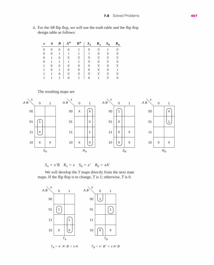
7.5 Solved Problems 467
ii. For the SR flip flop, we will use the truth table and the flip flopdesign table as follows:
x A B A� B� SA RA SB RB
0 0 0 0 1 0 X 1 00 0 1 1 1 1 0 X 00 1 0 X X X X X X0 1 1 1 1 X 0 X 01 0 0 0 0 0 X 0 X1 0 1 0 0 0 X 0 11 1 0 X X X X X X1 1 1 0 1 0 1 X 0
The resulting maps are
0 1x
A B
1
X
SA
X
X
00
01
11
10
0 1x
A B
X
X X
X
RA
1
X
00
01
11
10
0 1x
A B
X
1
X
SB
XX
X
00
01
11
10
0 1x
A B
1
X
X
RB
X
00
01
11
10
SA � x�B RA � x SB � x� RB � xA�
We will develop the T maps directly from the next statemaps. If the flip flop is to change, T is 1; otherwise, T is 0.
0 1x
A B
1
X
TA
TA � x � A� B � x A
1
X
00
01
11
10
TB � x � B� � x A� B
TB
0 1x
A B
1
1
XX
00
01
11
10
mar91647_c07b_466_492.qxd 11/24/08 10:10 AM Page 467

Finally, we will derive the JK inputs using the quickmethod. The maps below show the J section of the mapshaded.
JA � x�B KA � x JB � x� KB � xA�
Note that these are the same equations as those for the SR flipflop and the same amount of logic as is required for the D flipflop. Only the T flip flop requires significantly more logic.
A block diagram of the system with JK flip flops follows.
0 1x
XX
1
00
01
11
10
1
A B 0 1
1
1 1
00
01
11
10
1
XX
xA B
A B★ ★
J B
B�K
J A
A�K
x
Clock
z
468 Chapter 7 The Design of Sequential Systems
b. We can go to the truth table or we can first map A� and B� tofind the D inputs. The output is only a two-variable problem.We do not need to map that to recognize that
z � A � B
The truth table is shown (with columns for all types of flipflops).
mar91647_c07b_466_492.qxd 11/24/08 10:10 AM Page 468

7.5 Solved Problems 469
Maps for each of the functions are shown below (where DA isjust A�).
x A B A� B� SA RA SB RB TA TB JA KA JB KB
0 0 0 1 0 1 0 0 X 1 0 1 X 0 X0 0 1 0 0 0 X 0 1 0 1 0 X X 10 1 0 0 1 0 1 1 0 1 1 X 1 1 X0 1 1 1 0 X 0 0 1 0 1 X 0 X 11 0 0 0 0 0 X 0 X 0 0 0 X 0 X1 0 1 1 1 1 0 X 0 1 0 1 X X 01 1 0 1 1 X 0 1 0 0 1 X 0 1 X1 1 1 0 1 0 1 X 0 1 0 X 1 X 0
0 1
00
01
11
10
xA B
DA DB SA RA SB RB
1
1
1
1
0 1
00
01
11
10
xA B
1
11
1
0 1
00
01
11
10
xA B
1
X
1
X
0 1
00
01
11
10
xA B
X
1
X
1
0 1
00
01
11
10
xA B
X
11
X
0 1
00
01
11
10
xA B
1
XX
1
0 1
00
01
11
10
xA B
TA TB JA KA JB KB
1
1
1
1
0 1
00
01
11
10
xA B
1
11
1
0 1
00
01
11
10
xA B
1
XX
1
X X
0 1
00
01
11
10
xA B
X X
1
XX
1
0 1
00
01
11
10
xA B
XX
1 X X1
XX
0 1
00
01
11
10
xA B
1
XX
1
The corresponding equations are
z � A � B
DA � x�A�B� � x�AB � xA�B � x AB�
DB � xB � AB�
SA � x�A�B� � xA�B RA � x�AB� � xAB
SB � AB� RB � x�B
TA � x�B� � xB TB � x�B � AB�
JA � KA � x�B� � xB JB � A KB � x�
Note that the logic required to implement the JK flip flop solutionis the least, followed by the T and the SR, with the D requiringthe most. A block diagram of the JK solution is shown below. Tomake the drawing clearer, we put flip flop B on the left.
mar91647_c07b_466_492.qxd 11/24/08 10:10 AM Page 469
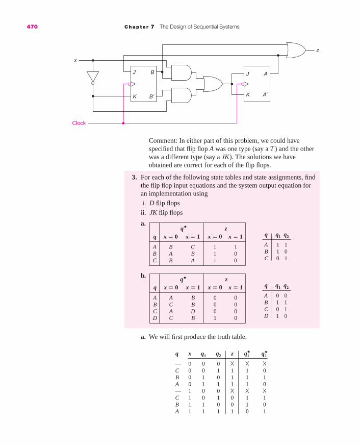
470 Chapter 7 The Design of Sequential Systems
J A
A�K
J B
B�K
x
Clock
z
q x q1 q2 z q1� q2
�
— 0 0 0 X X XC 0 0 1 1 1 0B 0 1 0 1 1 1A 0 1 1 1 1 0— 1 0 0 X X XC 1 0 1 0 1 1B 1 1 0 0 1 0A 1 1 1 1 0 1
Comment: In either part of this problem, we could havespecified that flip flop A was one type (say a T ) and the otherwas a different type (say a JK). The solutions we haveobtained are correct for each of the flip flops.
3. For each of the following state tables and state assignments, findthe flip flop input equations and the system output equation foran implementation using
i. D flip flops
ii. JK flip flops
a.
b.
a. We will first produce the truth table.
q� zq x � 0 x � 1 x � 0 x � 1
A A B 0 0B C B 0 0C A D 0 0D C B 1 0
q q1 q2
A 1 1B 1 0C 0 1
q q1 q2
A 0 0B 1 1C 0 1D 1 0
q� zq x � 0 x � 1 x � 0 x � 1
A B C 1 1B A B 1 0C B A 1 0
mar91647_c07b_466_492.qxd 11/26/08 12:22 PM Page 470

7.5 Solved Problems 471
i. We can now map z, D1 (q1�) and D2 (q2
�)
0 1x
q1 q2
z
z � x� � q1 q2
XX
1
1
1
1
00
01
11
10
D1 � x� � q1� � q2�
D1
X X
0 1
00
01
11
10
xq1 q2
11
1
1 1
D2 � x� q2� � x q2
D2
0 1
1
1
1
00
01
11
10
xq1 q2
XX
ii. Using the quick method, we look at the shaded part of themaps for J and the unshaded parts for K. (z is unchanged.)
0 1x
q1 q2
J1 � 1 K1 � x q2 J2 � x� K2 � x�
XX
1
1 1
11
00
01
11
10
X X
0 1
00
01
11
10
xq1 q2
1
1
1
b. We will first produce the truth table.
q x q1 q2 z q1� q2
�
A 0 0 0 0 0 0C 0 0 1 0 0 0D 0 1 0 1 0 1B 0 1 1 0 0 1A 1 0 0 0 1 1C 1 0 1 0 1 0D 1 1 0 0 1 1B 1 1 1 0 1 1
mar91647_c07b_466_492.qxd 11/24/08 10:10 AM Page 471

We do not need to map z, since it is clear from the truth tablethat
z � x�q1 q�2
i. We can now map D1(q1�) and D2(q2
�)
ii. For JK flip flops, we get
J1 � x K1 � x� J2 � x � q1 K2 � q�1
4. For the state table and each of the state assignments shown,design a system using D flip flops.
0 1x
q1 q2
D1 � x D2 � x q2� � q1
1
1
1
1
00
01
11
10
D2D1
1
0 1
00
01
11
10
xq1 q2
1 1
11
472 Chapter 7 The Design of Sequential Systems
a. b. c.
Each part of this is really a separate problem. (As we will see in Chapter 9, these are the only three assignments that producesignificantly different hardware. Each of the other possible state assignments involve either interchanging variables orcomplementing variables or both.) Compare the amount ofcombinational logic for each state assignment.
q q1 q2
A 0 0B 0 1C 1 0D 1 1
q q1 q2
A 0 0B 0 1C 1 1D 1 0
y q1 q2
A 0 0B 1 1C 1 0D 0 1
q� zq x � 0 x � 1 x � 0 x � 1
A B C 1 0B D A 0 0C B C 1 1D D A 1 0
mar91647_c07b_466_492.qxd 11/24/08 10:10 AM Page 472

7.5 Solved Problems 473
a. Since the assignment is in normal binary order, it is easy to godirectly to the maps.
0 1x
q1 q2
D1 � x� q2 � x q2�
1
1
1
1
00
01
11
10
D1
D2 � x�
D2
1
1
0 1
00
01
11
10
xq1 q2
1
1
z � x� q1 � x� q2� � q1 q2�
z
1
0 1
00
01
11
10
xq1 q2
1 1
1
0 1x
q1 q2
1
1
1
1
00
01
11
10
D1 D2
1 1
0 1
00
01
11
10
xq1 q2
1 1
D1 � x� q1� q2 � x� q1 q2� � x q1� q2� � x q1 q2
D2 � q1� q2� � q1 q2 z �x� q2� � q1 q2
z
1
0 1
00
01
11
10
xq1 q2
1
1 1
b. This assignment is in map order and once again we will godirectly to the maps without first producing a truth table.
where the brown terms are shared between D2 and z.
c. For this part, we will first construct the truth table and then goto the maps.
q x q1 q2 z q1� q2
�
A 0 0 0 1 1 1D 0 0 1 1 0 1C 0 1 0 1 1 1B 0 1 1 0 0 1A 1 0 0 0 1 0D 1 0 1 0 0 0C 1 1 0 1 1 0B 1 1 1 0 0 0
mar91647_c07b_466_492.qxd 11/24/08 5:03 PM Page 473

474 Chapter 7 The Design of Sequential Systems
0 1x
q1 q2
11
1 1
00
01
11
10
D1 D2
1
1
0 1
00
01
11
10
xq1 q2
1
1
D1 � q2� D1 � x� z � x� q1� � q1 q2�
z
1
1
0 1
00
01
11
10
xq1 q2
1 1
We really did not need to map D1 and D2; we should be able tosee those from the truth table.
Comparing the three solutions we see a major difference,based on the three state assignments.
a. 8 gates 16 inputsb. 11 gates 27 inputsc. 4 gates 7 inputs
5. Design a synchronous counter that goes through the sequence
1 3 5 7 4 2 0 6 and repeat
using D flip flops.
The truth table is shown below.
A B C A� B� C�
0 0 0 1 1 00 0 1 0 1 10 1 0 0 0 00 1 1 1 0 11 0 0 0 1 01 0 1 1 1 11 1 0 0 0 11 1 1 1 0 0
The maps for the D inputs are shown next, with the possibleshared terms circled in brown and tan.
0 1
00
01
11
10
A
B C
1
1
11
0 1
00
01
11
10
A
B C
11
1 1
0 1
00
01
11
10
A
B C
11
1
1
A B C★ ★ ★
mar91647_c07b_466_492.qxd 11/24/08 10:10 AM Page 474

7.5 Solved Problems 475
6. Design a synchronous counter that goes through the sequence
2 6 1 7 5 and repeat
using
i. D flip flops
ii. JK flip flops
Show a state diagram, indicating what happens if it initially is inone of the unused states (0, 3, 4) for each of the designs.
The truth table is shown below. The next state for unused states isshown as don’t cares.
A B C A� B� C�
0 0 0 X X X0 0 1 1 1 10 1 0 1 1 00 1 1 X X X1 0 0 X X X1 0 1 0 1 01 1 0 0 0 11 1 1 1 0 1
The maps and equations for the D inputs are shown next.
DA � A� � BC
DB � A� � B�
DC � AB � {A�B� or A�C}
There are two equally good solutions for DC; as we will seeshortly, the behavior of the system is different for those choicesif it is initialized to one of the unused states.
0 1
00
01
11
10
A
B C
1
X X
1X
1
X
1
0 1
00
01
11
10
A
B C
11
X X X X
0 1
00
01
11
10
A
B C
1
1
X 1
A B C★ ★ ★
DB is clearly B�. If we solve for the other two inputs independently,we get
DA = AC + BC DC = A�C + B�C
But, we can save a gate by sharing in either of two ways:
DA = AC + A�BC DC = A�BC + B�C or
DA = AB�C + BC DC = A�C + AB�C
mar91647_c07b_466_492.qxd 11/24/08 10:10 AM Page 475

Substituting the values for the three states not in the cycle:
0 (000): DA � 1, DB � 1, DC � 1 or DC � 0
3 (011): DA � 1, DB � 1, DC � 0 or DC � 1
4 (100): DA � 0, DB � 1, DC � 0
where the color indicates that the next state depends upon thechoice for the second term of DC.
The state diagrams for the two solutions are shown below.
476 Chapter 7 The Design of Sequential Systems
7
5
24
1
6
3
0 7
5
24
1
6
0
3
ii. The maps for the JK solution, with the J section shaded, andthe equations are shown below.
JA � 1 KA � B� � C�
JB � 1 KB � A
JC � A KC � AB�
Substituting the values for the three states not in the cycle:
0 (000): JA � KA � 1, JB � 1, KB � 0,
JC � KC � 0 ⇒ 110
3 (011): JA � 1, KA � 0, JB � 1, KB � 0,
JC � KC � 0 ⇒ 111
4 (100): JA � KA � 1, JB � KB � 1,
JC � KC � 1 ⇒ 011
0 1
00
01
11
10
A
B C
1
X X
1X
1
X
1
0 1
00
01
11
10
A
B C
11
X X X X
0 1
00
01
11
10
A
B C
1
1
X 1
A B C★ ★ ★
mar91647_c07b_466_492.qxd 11/24/08 10:10 AM Page 476
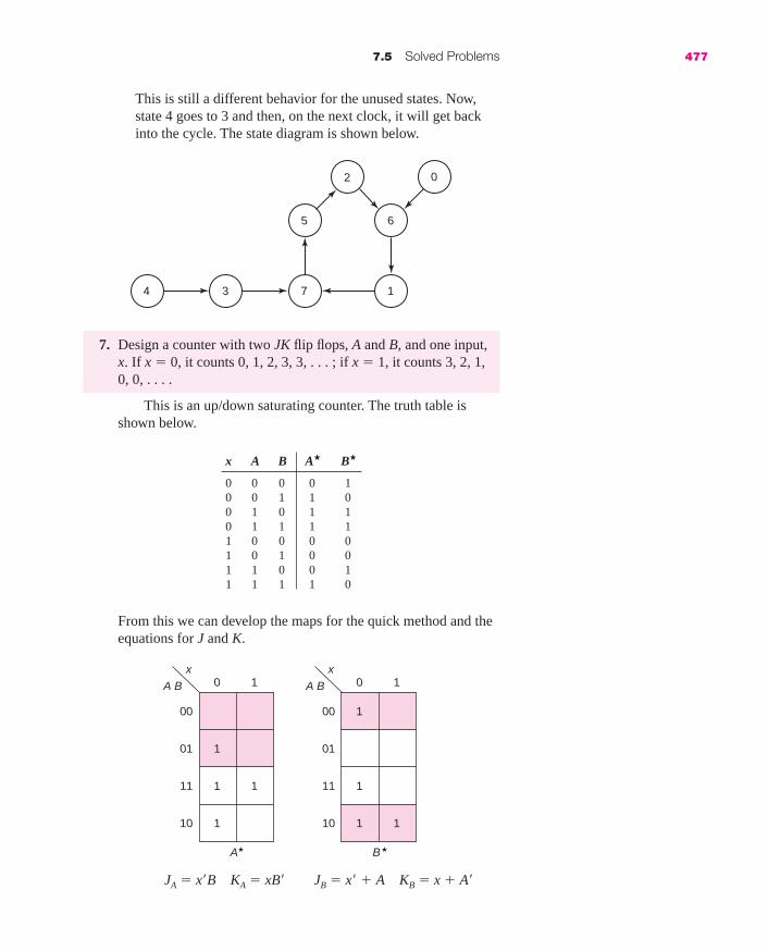
7.5 Solved Problems 477
This is still a different behavior for the unused states. Now,state 4 goes to 3 and then, on the next clock, it will get backinto the cycle. The state diagram is shown below.
7. Design a counter with two JK flip flops, A and B, and one input,x. If x � 0, it counts 0, 1, 2, 3, 3, . . . ; if x � 1, it counts 3, 2, 1,0, 0, . . . .
This is an up/down saturating counter. The truth table isshown below.
7
5
2
1
6
0
34
x A B A� B�
0 0 0 0 10 0 1 1 00 1 0 1 10 1 1 1 11 0 0 0 01 0 1 0 01 1 0 0 11 1 1 1 0
From this we can develop the maps for the quick method and theequations for J and K.
JA � x�B KA � xB� JB � x� � A KB � x � A�
0 1
00
01
11
10
A★
x
A B
1
11
1
1
1 1
0 1
00
01
11
10
B★
x
A B
1
mar91647_c07b_466_492.qxd 11/24/08 10:10 AM Page 477

8. Construct a base 60 (0 to 59) asynchronous counter using JKflip flops.
We need six flip flops and must detect when the count reaches60 and reset the counter. (That occurs when FEDC � 1.)
478 Chapter 7 The Design of Sequential Systems
JD
CLR� K
JC
CLR� K
JB
CLR� K
J 1
Clock
A
CLR� K
JE
CLR� K
JF
CLR� K
9. For each of the following problems show a state table or a statediagram. (A sample input/output trace is shown for each.)
a. A Mealy system that produces a 1 output iff there have beenfour or more consecutive 1 inputs or two or more consecutive0 inputs. (4 states)
x 0 1 1 0 0 1 0 0 1 1 1 1 1 0 0 0 1
z ? 0 0 0 1 0 0 1 0 0 0 1 1 0 1 1 0 0
b. A Mealy system whose output is 1 iff the last three inputswere 010. (3 states)
i. assuming overlapping is allowed
ii. assuming overlapping is not allowed
x 1 1 0 1 0 1 0 1 0 0 1 0 0 1 0 0 1 1 0
z-i 0 0 0 0 1 0 1 0 1 0 0 1 0 0 1 0 0 0 0 0
z-ii 0 0 0 0 1 0 0 0 1 0 0 1 0 0 1 0 0 0 0 0
c. A Mealy system whose output is 1 iff the last four inputs were1100 or the last output was a 1 and it is continuing on that pat-tern. (7 states)
x 1 0 1 1 0 0 1 0 1 1 0 0 1 1 0 0 1 1 1 0 0 1 0
z ? ? 0 0 0 1 1 0 0 0 0 1 1 1 1 1 1 1 0 0 1 1 0 0 0 0
d. A Moore system whose output changes whenever it detects asequence 110. (Assume that initially the output is 0.) (6 states)
x 0 0 1 0 1 1 1 0 1 1 0 0 1 1 0 1 0 1
z 0 0 0 0 0 0 0 0 1 1 1 0 0 0 0 1 1 1 1 1
e. A Moore system whose output is 1 iff the input has beenalternating for at least four clock periods. (8 states)
x 0 0 1 0 1 1 0 1 0 1 0 1 0 0
z ? ? 0 0 0 1 0 0 0 1 1 1 1 1 0
mar91647_c07b_466_492.qxd 11/24/08 10:10 AM Page 478
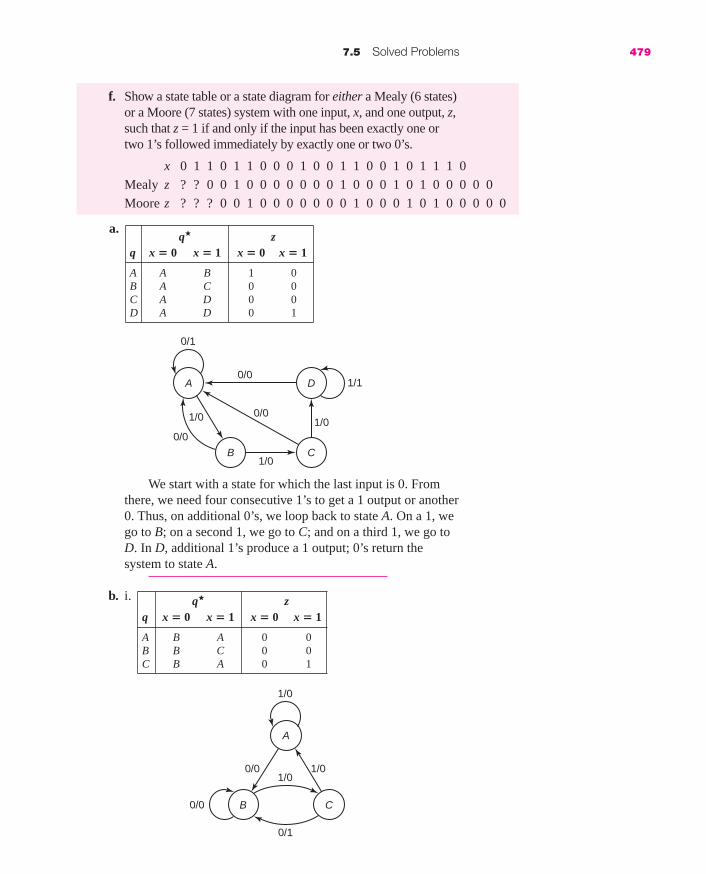
7.5 Solved Problems 479
f. Show a state table or a state diagram for either a Mealy (6 states)or a Moore (7 states) system with one input, x, and one output, z,such that z = 1 if and only if the input has been exactly one ortwo 1’s followed immediately by exactly one or two 0’s.
x 0 1 1 0 1 1 0 0 0 1 0 0 1 1 0 0 1 0 1 1 1 0
Mealy z ? ? 0 0 1 0 0 0 0 0 0 0 1 0 0 0 1 0 1 0 0 0 0 0
Moore z ? ? ? 0 0 1 0 0 0 0 0 0 0 1 0 0 0 1 0 1 0 0 0 0 0
We start with a state for which the last input is 0. Fromthere, we need four consecutive 1’s to get a 1 output or another0. Thus, on additional 0’s, we loop back to state A. On a 1, wego to B; on a second 1, we go to C; and on a third 1, we go toD. In D, additional 1’s produce a 1 output; 0’s return thesystem to state A.
b. i.
q� zq x � 0 x � 1 x � 0 x � 1
A A B 1 0B A C 0 0C A D 0 0D A D 0 1
1/1
1/0
1/0 1/0
0/1
0/0
0/0
0/0
B C
A D
q� zq x � 0 x � 1 x � 0 x � 1
A B A 0 0B B C 0 0C B A 0 1
0/0
1/0
1/0
1/00/0
0/1
B C
A
a.
mar91647_c07b_466_492.qxd 11/24/08 10:10 AM Page 479

State A is the “nowhere” state, where we are looking forthe first 0 in the pattern. A 0 gets us to B and then a 1 gets us toC. From there, a 0 input produces a 1 output. Since overlappingis allowed, that 0 input is the first 0 in a new string, and, thus,we return to state B.
In the case where overlapping is not allowed, we go fromstate C back to state A on a 0 input, since we are now nowhere,looking for a 010 pattern, as shown on the state diagrambelow.
c. If we start with the “nowhere” state, that is, where the outputis to be 0 and we are looking for the first 1, the success pathconsists of 1 1 0 0, at which point the output goes to 1. If thatis followed by a 1, the output remains 1. It also remains 1 ifthere is another 1 input and then a 0 input (which gets thesystem back to state D). That produces the following start forthe state diagram.
Now we can complete the failed paths. When we get a 0while we are looking for 1’s in states A, B, E, and F, wereturn to state A. We go next to state C on a 1 from either Cor G (when there are more than two 1’s in a row) and we goto B from D on a 1. Of course, all of these failed inputs
0/1
0/1
1/1
D E
F
1/1
G
0/0C
1/0
B
1/0
A
0/01/0
1/0
1/00/1
0/0
B C
A
480 Chapter 7 The Design of Sequential Systems
mar91647_c07b_466_492.qxd 11/24/08 10:10 AM Page 480

7.5 Solved Problems 481
produce a 0 output. The state diagram and then the state tableare shown below.
C0
B0
E1
D1
A0
F1
1
1
1
1
1
1
0
0 0
0
0
0
q�
q x � 0 x � 1 z
A A B 0B A C 0C D C 0D D E 1E D F 1F A F 1
d. For a Moore system, the output is associated with the state.There are two “nowhere” states, A and D, one for which theoutput is 0 and another for which the output is 1. The statediagram and table are as follows:
0/1
0/1 1/1
D E
F
1/1
G
0/0C
1/01/0
1/0
B
1/0 1/0
A
0/0
0/0
0/0
0/0
q� z
q x � 0 x � 1 x � 0 x � 1
A A B 0 0B A C 0 0C D C 0 0D E B 1 0E A F 0 1F A G 0 1G D C 1 0
mar91647_c07b_466_492.qxd 11/24/08 10:10 AM Page 481

When in the “nowhere” state and the input is 0, the systemremains there. It progresses on the first 1 to B or E and on thesecond 1 to C or F. The system remains in C or F if 1’scontinue, and goes to the “nowhere” state with the oppositeoutput on a 0 input.
e. We start with two “nowhere” states: A when the input has been0 for two or more consecutive inputs, and B when it has been 1for two or more consecutive inputs. From each of these thereis a separate success path (from A to C to E to G or from B toD to F to H). States G and H have a 1 output. If the inputcontinues to alternate, the system goes back and forth betweenthese two states.
482 Chapter 7 The Design of Sequential Systems
A0
B0
C0
D0
0
E0
F0
1
1
1
0
0
1
1 0
01
0
G1
H1
10
10
f. For both versions, the “nowhere” state, A, is when we arelooking for the first 1 input. The first 1 gets us to B, and thesecond, to C. State D is reached when we have had exactly oneor two 1’s (from B or C). In the Mealy version (on the left), theoutput is 1 when the system is in state D and the input is 1 oris 0 followed by a 1. That 1 is treated as the first 1 of a newinput sequence. The Moore version gets to state F after thesame sequence, where the output is 1. After too many 0’s(from state C), they go to F (Mealy) or G (Moore); after more than two 0’s in a row, the systems return to state A.
mar91647_c07b_466_492.qxd 11/24/08 10:10 AM Page 482

7.6 Exercises 483
7.6 EXERCISES
1. Find equations for q★
1, q★
2, and Z for the state table of Figure 7.1,using the state assignment of Table 7.1c.
2. For each of the following state tables, design the system using
i. D flip flops
ii. SR flip flops
iii. T flip flops
iv. JK flip flops
Show the equations for each and a block diagram for the JK design(using AND, OR, and NOT gates).
A0
E0
D0
F1
B0
G 0
C0
A
F
B E
C D0/0
0/0
0/0
0/0
0/0
0/0
1/0 1/0
1/1
1/11/0
1/0
0
0
0
0
1
111
1
1
1
0
00
b.
�a.A� B� z
A B x � 0 x � 1 x � 0 x � 1
0 0 1 1 0 0 0 10 1 0 1 0 0 1 01 1 0 1 1 1 1 0
A� B� zA B x � 0 x � 1 x � 0 x � 1
0 0 1 0 1 1 0 00 1 0 0 0 1 0 01 0 0 1 1 1 1 01 1 0 0 0 0 1 1
EX
ER
CIS
ES
mar91647_c07b_466_492.qxd 11/24/08 10:10 AM Page 483

g.
�f.
e.
d.
c.
484 Chapter 7 The Design of Sequential Systems
A� B�
A B x � 0 x � 1 z
0 0 1 0 0 0 00 1 0 0 1 1 11 0 0 1 0 1 11 1 0 0 0 1 1
A� B�
A B x � 0 x � 1 z
0 0 1 1 1 0 00 1 1 0 1 0 11 0 1 1 0 0 11 1 0 1 1 1 1
A� B�
A B x � 0 x � 1 z
0 0 1 0 0 1 10 1 1 1 0 0 11 0 0 0 1 1 01 1 0 1 0 0 0
A� B� C� zA B C x � 0 x � 1 x � 0 x � 1
0 0 0 0 0 1 0 0 0 1 10 0 1 0 1 0 0 0 0 1 10 1 0 0 1 1 0 0 0 1 10 1 1 1 0 0 0 0 0 1 11 0 0 1 0 1 0 0 0 1 11 0 1 1 0 1 0 0 0 0 1
A� B�
A B x � 0 x � 1 z
0 0 0 1 0 0 00 1 1 1 0 0 11 1 0 0 0 1 1
EX
ER
CIS
ES
mar91647_c07b_466_492.qxd 11/24/08 10:10 AM Page 484

7.6 Exercises 485
q�
q x � 0 x � 1 z
A C B 1B C A 1C A C 0
q q1 q2
A 1 1B 0 1C 1 0
q�
q x � 0 x � 1 z
A B C 1B A B 0C B A 0
q q1 q2
A 0 0B 1 0C 0 1
q� zq x � 0 x � 1 x � 0 x � 1
A C B 1 1B A A 1 0C C A 1 0
q q1 q2
A 0 0B 1 1C 0 1
q� zq x � 0 x � 1 x � 0 x � 1
A B B 0 0B D A 1 0C D B 0 0D C D 1 0
q q1 q2
A 0 0B 1 1C 1 0D 0 1
3. For each of the following state tables and state assignments, findthe flip flop input equations and the system output equation for animplementation using
i. D flip flops
ii. JK flip flops
a.
b.
c.
d.
b.
�
q� zq x � 0 x � 1 x � 0 x � 1
A B D 0 0B D C 1 0C A B 0 0D C A 1 0
q q1 q2
A 0 0B 0 1C 1 1D 1 0
e.
EX
ER
CIS
ES
mar91647_c07b_466_492.qxd 11/24/08 10:10 AM Page 485

486 Chapter 7 The Design of Sequential Systems
q q1 q2
A 0 0B 0 1C 1 0D 1 1
q q1 q2
A 0 0B 0 1C 1 1D 1 0
q q1 q2
A 0 0B 1 1C 1 0D 0 1
4. a. For the state table and each of the state assignments shown,design a system using D flip flops.
q� zq x � 0 x � 1 x � 0 x � 1
A B C 1 0B A B 0 1C B B 0 0
q� zq x � 0 x � 1 x � 0 x � 1
A A C 0 0B C B 1 1C A B 1 0
i. ii. iii.
q q1 q2
A 0 0B 0 1C 1 0
q q1 q2
A 0 0B 0 1C 1 1
q q1 q2
A 0 0B 1 1C 1 0
b, c. For each of the state tables and each of the state assignmentsshown, design a system using D flip flops.
�b.
q�
q x � 0 x � 1 z
A B D 0B C A 1C B B 1D D C 1
c.
i. ii. iii.
EX
ER
CIS
ES
mar91647_c07b_466_492.qxd 11/24/08 10:10 AM Page 486

5. Complete the design of the 4-bit binary counter (from thebeginning of Section 7.2) with SR flip flops.
6. If we build the decade counter using JK flip flops, show a statediagram, including what happens if it initially is in one of theunused states (10, 11, 12, 13, 14, 15).
7. Design, using
i. D flip flops
ii. JK flip flops�a. a synchronous base-12 counter, one that goes through the
sequence
0 1 2 3 4 5 6 7 8 9 10 11 . . .
b. a synchronous binary down counter, one that goes through thesequence
15 14 13 12 11 10 9 8 7 6 5 4 3 2 1 0 . . .
8. Design synchronous counters that go through each of the followingsequences
a. 6 5 4 3 2 1 and repeat�b. 1 3 4 7 6 and repeat
c. 6 5 4 1 2 3 and repeat
d. 6 5 1 3 7 and repeat
e. 7 4 3 6 1 2 and repeat
f. 1 3 5 7 6 4 2 0 and repeat
using
i. JK flip flops
ii. D flip flops
Show a state diagram, indicating what happens if it initially is inone of the unused states for each of the designs.
9. Design a counter with two JK flip flops, A and B, and one input, x.If x � 0, it counts 1 3 0 and repeat; if x � 1, it counts 1 2 3 andrepeat.
a. Assume that x changes only when it is in state 1 or 3 (in whichcase there are two combinations which never occur—state 2and x � 0, and state 0 and x � 1).
b. After building the design of part a (with the two don’t cares),what happens if somehow x is 0 in state 2 and what happens ifsomehow x is 1 in state 0?
10. a. Design a counter with two JK flip flops (A and B) and an input(x) that counts 0 1 2 3 and repeat when x � 0 and counts 0 1 2and repeat when x � 1. Design this assuming that x never is 1when the count is 3. Show the minimum equations for each.
b. What does happen when x goes to 1 when the count is 3?
7.6 Exercises 487
�
EX
ER
CIS
ES
mar91647_c07b_466_492.qxd 11/24/08 10:10 AM Page 487

11. Design the system of CE10, using JK flip flops.
12. Design an asynchronous base-10 counter, using T flip flops with astatic active high clear.
13. Complete the design of CE6 using JK flip flops for the threedifferent state assignments of Table 7.1.
14. Design the three-state version of CE7, using D flip flops and eachof the following state assignments.
488 Chapter 7 The Design of Sequential Systems
q q1 q2
A 0 0B 0 1C 1 0
q q1 q2
A 0 0B 0 1C 1 1
q q1 q2
A 0 0B 1 1C 0 1
(a) (b) (c)
15. Design a system using JK flip flops that produces a 1 output iffthere have been exactly three 1’s in a row. (See Example 7.10.)
a. Using the Mealy state diagram.
b. Using the Moore state table.
16. For each of the following problems show a state table or a statediagram. (A sample input/output trace and the minimum number ofstates required is shown for each.)
a. A Moore system that produces a 1 output iff the input has been0 for at least two consecutive clocks followed immediately bytwo or more consecutive 1’s. (5 states)
x 0 1 0 0 1 0 0 1 1 0 0 0 1 0 1 0 0 0 1 1 1 1 0
z 0 0 0 0 0 0 0 0 0 1 0 0 0 0 0 0 0 0 0 0 1 1 1 0 0
�b. A Moore system, the output of which is 1 iff there have beentwo or more consecutive 1’s or three or more consecutive 0’s.(5 states)
x 0 0 0 0 1 0 1 1 0 0 1 1 1 0 0 0 1 0
z ? ? ? 1 1 0 0 0 1 0 0 0 1 1 0 0 1 0 0 0
c. A Mealy system that produces a 1 output iff the input has been1 for three or more consecutive clock times or 0 for three ormore consecutive clock times. When first turned on, it is in aninitial state A. (There are four additional states.)
x 0 0 0 0 1 0 1 1 0 0 0 1 1 1 1 1 0 0 1
z 0 0 1 1 0 0 0 0 0 0 1 0 0 1 1 1 0 0 0 0
d. A Mealy system that produces a 1 output iff the input has beeneither 0 1 0 or 1 0 1. Overlapping is allowed. When first turnedon, it is in an initial state A. (There are four additional states.)
EX
ER
CIS
ES
mar91647_c07b_466_492.qxd 11/24/08 10:10 AM Page 488

x 0 0 1 0 0 1 0 1 0 0 1 1 0 1 1 0 1 0 0
z 0 0 0 1 0 0 1 1 1 0 0 0 0 1 0 0 1 1 0 0
e. A Mealy system that produces a 1 output iff the input is 0 forthe first time after it has been 1 for at least two consecutiveclocks or when it is 1 after having been 0 for at least twoconsecutive clocks. Overlapping is allowed. When first turnedon, it is in an initial state A. (There are four additional states.)
x 0 1 0 0 0 1 1 1 1 1 0 0 1 1 0
z 0 0 0 0 0 1 0 0 0 0 1 0 1 0 1 0
f. A Mealy system, the output of which is 1 iff the input hadbeen at least two 0’s followed by exactly two 1’s followed by a0. Overlapping is not allowed. (5 states)
x 1 1 1 0 0 0 1 1 0 0 1 1 0 0 1 1 1 0 0 0 0 1 1 0 0
z 0 0 0 0 0 0 0 0 1 0 0 0 0 0 0 0 0 0 0 0 0 0 0 1 0 0 0
g. A Mealy system, the output of which is 1 iff there have beenexactly two consecutive 1’s followed by at least twoconsecutive 0’s. (5 states)
x 0 1 1 0 0 0 1 1 0 0 1 1 0 0 1 1 1 0 0 0 0 1 1 0 0
z ? 0 0 0 1 1 0 0 0 1 0 0 0 1 0 0 0 0 0 0 0 0 0 0 1
h. A Mealy system, the output of which is 1 iff there have beenexactly two consecutive 0’s or exactly two consecutive 1’s.
i. Overlapping is allowed (6 states)
ii. Overlapping is not allowed (6 states)
x 0 1 1 1 0 1 1 0 0 1 1 0 1 0 1 0 0 1
z-i ? ? 0 0 0 0 0 1 0 1 0 1 0 0 0 0 0 1 0
z-ii ? ? 0 0 0 0 0 1 0 0 0 1 0 0 0 0 0 1 0 0
i. A Mealy system, the output of which is 1 iff there has been apattern of 1 0 1 1.
i. Overlapping is allowed (4 states)
ii. Overlapping is not allowed (4 states)
x 0 0 1 0 1 1 0 1 1 0 1 1 1 0 0 1 0 1 0 1 1
z-i 0 0 0 0 0 1 0 0 1 0 0 1 0 0 0 0 0 0 0 0 1 0 0
z-ii 0 0 0 0 0 1 0 0 0 0 0 1 0 0 0 0 0 0 0 0 1 0 0 0
j. A Mealy system, the output of which is 0 iff there has been apattern of 1 1 0 1. (The output is 1 most of the time.)
i. Overlapping is allowed (4 states)
ii. Overlapping is not allowed (4 states)
7.6 Exercises 489
EX
ER
CIS
ES
�
mar91647_c07b_466_492.qxd 11/24/08 10:10 AM Page 489

x 0 0 1 0 1 1 0 1 1 0 1 1 1 0 0 1 0 1 1 0 1 1
z-i 1 1 1 1 1 1 1 0 1 1 0 1 1 1 1 1 1 1 1 1 0 1 1
z-ii 1 1 1 1 1 1 1 0 1 1 1 1 1 1 1 1 1 1 1 1 0 1 1 1
�k. A Mealy system, the output of which is 1 iff the input hascontained an even number of 0’s (including no 0’s) and amultiple of four 1’s (including no 1’s). When first turned on,the system is initialized to a state indicating no 0’s and no 1’s(but that state is reached again later). (8 states)
x 0 1 1 0 1 1 0 0 0 0 1 0 1 0 0 0 1 0 1 0
z 0 0 0 0 0 1 0 1 0 1 0 0 0 0 0 0 0 0 0 1 0
�l. A Moore system, the output of which is 1 iff the pattern 1 0 1has occurred more recently than 1 1 1. (6 states)
x 1 0 1 0 1 1 0 1 0 1 1 1 1 0 0 1 0 1 1 1
z ? ? ? 1 1 1 1 1 1 1 1 1 0 0 0 0 0 1 1 1 0 0
Determine from the sample whether overlapping is allowed.
m. A Mealy system, the output of which is 1 iff the input isexactly two 1’s followed immediately by exactly one or two 0’s. Full credit for solutions with six or less states.
x 1 0 0 1 1 0 0 1 1 0 1 1 1 0 0 1 1 0 0 0 0 0
z ? 0 0 0 0 0 0 1 0 0 1 0 0 0 0 0 0 0 0 0 0 0 0 0 0 0
n. A Mealy system, the output of which is 1 iff there has been apattern of 1 1 0 0 0. (5 states)
x 0 0 0 0 1 0 1 1 0 0 0 0 1 1 1 1 0 0 0 1
z ? ? ? 0 0 0 0 0 0 0 1 0 0 0 0 0 0 0 1 0 0 0 0
o. In this Mealy system, there are two inputs, a and b; they are tobe treated as a binary number, that is 00 is 0, 01 is 1, 10 is 2,and 11 is 3. The output is to be 1 if the current number isgreater than or equal to the previous one AND the previousone is greater than or equal to the one before that. It is to be 0otherwise. There is an initial state for which there have beenno previous numbers. Be sure to explain the meaning of eachstate. (8 states in addition to the initial one)
a 0 0 1 0 1 0 0 0 1 1 1 0 1 1
b 1 0 0 1 1 0 0 1 0 1 0 0 1 1
z 0 0 0 0 0 0 0 1 1 1 0 0 0 1
490 Chapter 7 The Design of Sequential Systems
EX
ER
CIS
ES
mar91647_c07b_466_492.qxd 11/24/08 10:10 AM Page 490

a. b.
7.7 Chapter 7 Test 491
q�
q x � 0 x � 1 z
A A B 1B B C 1C A C 0
q�
q x � 0 x � 1 z
A C B 1B D D 0C A D 0D C B 0
2. For the following state table and state assignment, design a systemusing an SR flip flop for q1 and a JK flip flop for q2. Show the flipflop input equations and the output equation; you do NOT need todraw a block diagram.
q q1 q2
A 0 0B 0 1C 1 0D 1 1
q q1 q2
A 0 0B 1 1C 0 1D 1 0
c. Show a block diagram for the solution to part b, using AND,OR, and NOT gates.
7.7 CHAPTER 7 TEST (75 MINUTES)
1. For the following state table, design a system using a D flip flop forA, a JK flip flop for B, and AND, OR, and NOT gates. Show theflip flop input equations and the output equation; you do NOT needto draw a block diagram.
q q1 q2
A 0 0B 1 0C 1 1
A�B� zA B x � 0 x � 1 x � 0 x � 1
0 0 1 1 0 1 0 10 1 0 0 1 0 0 01 0 1 0 0 1 1 11 1 0 1 1 0 1 0
3. For the following state table, design a system using D flip flops foreach of the state assignments. Show equations for D1, D2, and z.
CH
AP
TE
R T
ES
T
mar91647_c07b_466_492.qxd 11/24/08 10:10 AM Page 491

4. Design a counter that goes through the sequence
1 4 3 6 2 5 and repeat
using a D flip flop for A, a JK flip flop for B, and a T flip flop for C.
Five-point bonus: Show a state diagram, including what happensif the system is initially in state 0 or 7.
5. a. Show the state table or state diagram for a Mealy system thatproduces a 1 output if and only if the input has been 1 0 1 0for the last four clock times. Overlapping is allowed. (4 states)
b. Show the state table or state diagram for a Mealy system thatproduces a 1 output if and only if the input has been 1 0 1 0for the last four clock times. Overlapping is not allowed. (4 states)
Example:
x 1 1 0 1 0 1 1 1 0 1 0 1 0 1 0 0
z-a 0 0 0 0 1 0 0 0 0 0 1 0 1 0 1 0
z-b 0 0 0 0 1 0 0 0 0 0 1 0 0 0 1 0
6. Show the state table or state diagram for a Moore system thatproduces a 1 output if and only if the input has been 0 1 1 for thelast three clock times. (4 states)
Example:
x 0 0 1 0 1 1 1 0 0 1 1 0 1 1
z ? 0 0 0 0 0 1 0 0 0 0 1 0 0 1
492 Chapter 7 The Design of Sequential Systems
CH
AP
TE
R T
ES
T
mar91647_c07b_466_492.qxd 11/24/08 10:10 AM Page 492

493
Solving LargerSequential Problems
As we get to larger problems, data are often stored in registers,rather than individual flip flops. A register is just a collection offlip flops, often with a common name (using subscripts to indi-
cate the individual flip flops) and usually with a common clock. Forexample, in a computer, the two inputs to the adder (say 16 bits each)may come from two registers, each of which consists of 16 flip flops. Itis nearly impossible to show a block diagram of such a system with allof the individual flip flops and gates.
In this chapter, we will look first at two classes of commercialmedium-scale integrated circuits*—shift registers and counters. We willintroduce programmable logic devices with memory to implement morecomplex problems such as CPLDs and FPGAs. We will then look brieflyat two tools for dealing with these larger systems, ASM (AlgorithmicState Machine) diagrams and HDL (Hardware Design Languages).Lastly, we will then look at some larger design problems than we couldmanage in Chapter 7. We will concentrate on synchronous (clocked)systems.
8.1 SHIFT REGISTERS
A shift register, in its simplest form, is a set of flip flops, such that thedata moves one place to the right on each clock or shift input. A simple4-bit shift register is shown in Figure 8.1, using SR flip flops. (Althoughshift registers are most commonly implemented with SR flip flops, JKflip flops could be used in place of the SR’s in the same circuit. D flipflops could also be used; the q output of one flip flop would be connectedto the D input of the next.) At each clock, the input, x, is moved into q1,and the contents of each of the flip flops is shifted one place to the right.
*When we look at the details of some of these circuits, we will simplify the logicsomewhat by looking at just one bit and by eliminating some of the double NOT gatesthat are used for reducing load.
C H A P T E R
8
mar91647_c08_493_542.qxd 11/24/08 10:32 AM Page 493

494 Chapter 8 Solving Larger Sequential Problems
Figure 8.1 A simple shift register.
D q4
q4�
S q3x q2
Clock
S q1
R
S
Rq3�
q4
q4�q2�q1�R
S
R
A sample timing trace is shown in Trace 8.1, assuming that all flip flopsare initially 0. The sample input is shown in brown.
Trace 8.1 Shift register timing.
x 1 0 1 1 1 0 1 1 1 1 0 0 0q1 0 1 0 1 1 1 0 1 1 1 1 0 0 0q2 0 0 1 0 1 1 1 0 1 1 1 1 0 0 0q3 0 0 0 1 0 1 1 1 0 1 1 1 1 0 0 0q4 0 0 0 0 1 0 1 1 1 0 1 1 1 1 0 0 0
In some commercial shift registers, a NOT gate is added at the clockinput, as shown in Figure 8.2.
Figure 8.2 Leading-edge triggered shift register.
D q4
q4�
S q3x q2
Clock
S q1
R
S
Rq3�
q4
q4�q2�q1�R
S
R
This accomplishes two things. The shift register is now leading-edgetriggered (since the leading edge of the clock is the trailing edge of theflip flop input). Also, the clock input signal only goes to the NOT gate.Thus, this circuit presents a load of 1 to the clock, rather than a load of 4(if the signal went to all four flip flops). When a trailing-edge triggeredshift register is desired, a second NOT gate is added in series with theone shown. Sometimes, the x input is first inverted to present only a loadof 1. Both of these changes are shown in the circuit of Figure 8.3.
mar91647_c08_493_542.qxd 11/24/08 10:32 AM Page 494

This version of the shift register is referred to as serial-in, serial-outin that only 1 bit (the left bit) may be loaded into the register at a timeand, as shown, only 1 bit (the right bit) may be read. (Only the uncom-plemented value, q4, may be available or both the uncomplemented andcomplemented, q4 and q�4, may be outputs.) The main limitation on theamount of logic that can fit on a single chip is the number of input andoutput connections. Thus, one could build a serial-in, serial-out shift reg-ister with a nearly unlimited number of bits on a chip, since there areonly three or four logic connections.
One application of a large serial-in, serial-out shift register is amemory similar to a disk. If the output bit is connected back to the inputas shown in Figure 8.4, when Load is 0, the data circulate around the nflip flops. It is available only when it is in qn, once every n clock cycles.At that time it can be modified, by making Load � 1 and supplying thenew value on x. If we needed a series of 8-bit numbers, we could buildeight such shift registers, storing 1 bit in each. As we clocked all the shiftregisters, we would obtain 1 byte (8 bits) at a time.
8.1 Shift Registers 495
Figure 8.3 Shift register with load-reducing NOT gates.
D q4
q4�
S q3
x
q2
Clock
S q1
R
S
Rq3�
q4
q4�q2�q1�R
S
R
Figure 8.4 Shift register storage.
D q4
q4�
S q3
x
Loadq2
Clock
S q1
R
S
Rq3�
qn
qn�q2�q1�R
S
R
...
...
...
To initialize a 4-bit serial-in, serial-out shift register to all 0’s, wewould have to clock it four times, with 0 on input x each time. To avoidthis, most shift registers have an active low (usually static) clear input.Many shift registers have a parallel output, that is, the contents of eachof the flip flops is available. (Obviously, if we were building this with
mar91647_c08_493_542.qxd 11/24/08 10:32 AM Page 495

independent flip flops, this would just require connecting a wire to eachflip flop output. If, however, the whole shift register were contained on asingle integrated circuit, each output would require a pin.) There is an8-bit serial-in, parallel-out shift register on one chip, using D flip flops(74164); it uses the 12 logic connections for 8 outputs, the clock, theclear, and 2 for serial input, as shown in Figure 8.5. (The x is replaced byA B, two inputs into a built-in AND gate.)
496 Chapter 8 Solving Larger Sequential Problems
One application of a serial-in, parallel-out shift register is an inputport from a modem. Data are transmitted serially over telephone lines. Itis clocked into a shift register until a whole byte or word is received.Only then is there interaction with the computer’s memory; the group ofbits are read in parallel from the shift register and loaded into memory.
A parallel-in shift register allows the register to be loaded in onestep. That, of course, requires an input line for each flip flop, as well asa control line to indicate load. Sometimes the loading is done statically(74165), as demonstrated for a typical bit (q2) in Figure 8.6a. Sometimesit is done synchronously (74166), as shown in Figure 8.6b. Both of theseare serial-out, that is, there is only one output connection, from the rightflip flop. There is a serial input to the left bit for shift operations (goingto the same place in the first flip flop logic that q1 goes to in the typicalbit in Figure 8.6).
For the 74165, the clock input to the flip flops is inverted from theinput to the chip and passed through only when Load� is high (don’tload) and Enable� is low (enable shift). When Load� is high, both CLR�and PRE� are high, and the shift works. When Load� is low, the clock isdisabled, IN�2 appears on PRE�, and IN2 appears on CLR�, thus loadingIN2 into the flip flop.
For the 74166, there is an active low static clear, independent of theload. The clock is inverted when Enable� is 0; otherwise, the flip flopsare not clocked and nothing changes. When enabled and Load� is 0, IN2
is stored in q2; when Load� is 1 (inactive), q1 is shifted into q2.
Figure 8.5 74164 serial-in parallel-out shift register.
q2
Clock
DA
B
Clear �
q1
q1 q2 q3 q4 q5 q6 q7 q8
q2�q1�
D D q3
q3�
D q4
q4�
D q5
q5�
D q6
q6�
D q7
q7�
D q8
q8�
mar91647_c08_493_542.qxd 11/24/08 10:32 AM Page 496

The parallel-in, serial-out shift register is used in the output processfor serial data. A word is loaded (all at once) into the shift register fromthe computer. Then, bits are sent to the modem from the right end of theshift register one at a time.
Parallel-in, parallel-out shift register chips are limited to 4 or 5 bitsbecause of the number of connections required. The 7495 is very similarto the 74166 in control structure, except that it has a separate clock inputfor shifting and for loading.
In most computers, there are both left and right shift and rotate*
instructions. To implement these, we might use a right/left shift register(such as the 74194, a synchronous parallel-in, parallel-out 4-bit shift reg-ister). For this, a three-way multiplexer is needed at each bit, since thatbit can receive the bit to its left, the bit to its right, or the input bit. A truthtable describing the behavior of the shift register is shown in Table 8.1.Bits are numbered 1 to 4 from left to right.
8.1 Shift Registers 497
Figure 8.6 Parallel-in shift registers.
(a) 74165 (b) 74166
q2
IN2
q1
q2�q1�
SPRE�
CLR�R
Clock
Enable�
Load�
q2q1
q2�
S
R
IN2
CLR�
Clock
Enable�
Load�
Clear �
*A one place right rotate moves every bit one place to the right and moves the right-mostbit back into the left flip flop.
Table 8.1 Right/left shift register.
Clear� S0 S1 q1� q2
� q3� q4
�
Static clear 0 X X 0 0 0 0Hold 1 0 0 q1 q2 q3 q4
Shift left 1 0 1 q2 q3 q4 LSShift right 1 1 0 RS q1 q2 q3
Load 1 1 1 IN1 IN2 IN3 IN4
mar91647_c08_493_542.qxd 11/24/08 10:32 AM Page 497

x A B C D E F G H
ck
Note that when S0 and S1 are both 0, the clock input to the flip flop is 0;there is no edge, and thus the flip flop holds. Otherwise, the clock isinverted and thus this is a leading-edge triggered shift register. (Note thatfor q1, the left flip flop, RS comes into the top input of the multiplexer,and for q4, LS comes into the bottom input.)
As an example of an application of shift registers, consider the fol-lowing problem.
We want to design a system with one output, z, which is 1 if the input, x,has been alternating for seven clock times (including the present). We haveavailable an 8-bit serial-in, parallel-out shift register as shown below:
498 Chapter 8 Solving Larger Sequential Problems
Figure 8.7 Right/left shift register.
q1
q3
S0
S1
IN2 q2�
q2S
RCLR�
Clock
Clear �
EXAMPLE 8.1
Where the INi are the inputs for parallel load, RS is the serial input for aright shift, and LS is the serial input for a left shift. The hold combinationis really the “don’t shift, don’t load” input. A typical bit (with the controlcircuitry) is shown in Figure 8.7.
(The shift register probably also has a static clear input, but it is not neededfor this problem.)
mar91647_c08_493_542.qxd 11/24/08 10:32 AM Page 498

At any time, the register contains the value of x at the eight most recentclocks, with the most recent in A and the oldest in H. For this problem, weonly need six of these. The circuit below computes the answer.
8.2 Counters 499
x x
Clock
A B C D E F G H
ck
z
8.2 COUNTERS
In Chapter 7, we discussed the design of counters. In this section, we willlook at some of the commercially available counters and applications ofcounters. A counter consists of a register and the associated logic.
Counters may be synchronous or asynchronous and may be base 10,12, or 16 (that is, cycle through 10, 12, or 16 states on consecutive clockpulses). Most synchronous counters have parallel loads; they may bepreset to a value, using the load signal and an input line for each bit.Many also have a clear (or Master Reset) signal to load the register withall 0’s. These control signals are usually active low; they may be syn-chronous or asynchronous. Most asynchronous counters just have astatic clear. In addition, some synchronous counters count both up anddown. Most counters have a carry or overflow output, which indicatesthat the counter has reached its maximum and is returning to 0 (for upcounters). That may be a logic 1, or it may be a clock pulse coincidentwith the pulse that causes the transition back to 0.
We will first look at the 74161 counter, which does synchronouscounting and loading and has an asynchronous (active low) clear. It hastwo count enables, ENT and ENP* (both of which must be 1 to enable
[SP 1, 2, 4a; EX 1, 2, 4b; LAB]
*Only ENT enables the overflow output.
mar91647_c08_493_542.qxd 11/24/08 10:32 AM Page 499

We could use two of these counters to count to 255 (28 � 1) or threeto count to 4095 (212 � 1). The block diagram of Figure 8.9 illustratesthe 8-bit counter, where no parallel load inputs are shown.
If the counter is cleared initially, only the low-order counter (the oneon the right) is enabled for the first 15 clocks. When that counter reaches
500 Chapter 8 Solving Larger Sequential Problems
Figure 8.8 The 74161 counter.
J
wx
B
AENT
ENP
Load�
INCz
C
C�
CLR�
Clear �
K
y
Clock
D C B A ENT
ENP
Clock
OV
74161
CLR�
Load�INAINBINCIND
counting). Labeling the bits D (high), C, B, and A, a block representationof the counter and the logic for a typical bit, bit C, is shown in Figure 8.8.Since the clock is inverted before going to the trailing-edge triggered flipflop, the counter is leading-edge triggered. The only difference betweenbits is the inputs to the brown AND gate. That is the value for the J andK inputs to each bit when counting (ANDed with the enable). (Thus, D’sinput is A B C, C’s input is A B, B’s input is A, and A’s input is 1.) Whenloading (Load� � 0), point x is 1, point y is 1, point z equals IN�C, andpoint w equals INC. Thus, the flip flop is loaded with the value on INC.When Load� � 1, then point x equals 0, points w and z equal 1, and point yis just the output of the brown AND gate. Thus, J and K are 1 when thebrown gate output is 1, that is, when this flip is to change during thecount.
mar91647_c08_493_542.qxd 11/24/08 10:32 AM Page 500

D
O7 O6 O5 O4
C B A
ENP
Clock
ENTCLR�
OV High
LD�
D
O3 O2 O1 O0
C B A
1
ENPENTCLR�
OV Low
LD�
15 (1111), the overflow output (OV ) becomes 1. That enables the secondcounter. On the next clock, the right counter goes to 0 (returning OV to0) and the left counter increases by 1. (Thus, the count reaches 16.) Onlythe low-order counter increments on the next 15 clocks, as the countreaches 31. On the 32nd clock, the high-order counter is enabled again.
If we wanted to count through a number of states other than a power of 16,we would need to reset the counter when we reached the desired maxi-mum. Since the 74161 counter has a static clear (similar to the asynchro-nous counter example in Example 7.9), we must count one beyond thedesired maximum and use that to clear the counter. We will thus reach theextra state for a brief time (before the clear is effective), but that is wellbefore the next clock time. For example, the counter of Figure 8.9 could beused to count through 120 states (0 to 119) by adding the NAND gateshown to clear it when it reaches 120 (01111000).
8.2 Counters 501
Figure 8.9 8-bit counter.
D
O7 O6 O5 O4
C B A
ENP
Clear�
Clock
ENTCLR�
OV High
LD�
D
O3 O2 O1 O0
C B A
1
ENPENTCLR�
OV Low
LD�
EXAMPLE 8.2
We do not need to AND O�2, O�1, O�0, or O�7, since we never reach a countover 120, and thus these are never 1 when O6, O5, O4, and O3 are all 1.
mar91647_c08_493_542.qxd 11/24/08 10:32 AM Page 501

The 74163 is similar to the 74161, except that the clear is clocked. Theinternal structure of the circuit is modified so that an active clear input loadsa 0 into each flip flop on the clock. To use it in a 120 state counter, we needto detect 119 and reset it on the next clock pulse, as shown below. Theadvantage of this approach is that there is no period (not even a short one)where the counter reaches 120.
502 Chapter 8 Solving Larger Sequential Problems
There are decade counters (counting 0 to 9) similar to the two binarycounters we just described (74160 with a static clear and 74162 with aclocked clear).
There are both binary (74191 and 74193) and decade (74190 and74192) up/down counters. The first of each type has a single clock inputand a Down/Up� input (where a 1 indicates down and a 0 indicates up).The second has two separate clock inputs, one for counting down and theother for counting up; one of those must be a logic 1 for the other towork. All of these have static load inputs. Bit C of the 74191 binarycounter is shown in Figure 8.10. When Load� is 0, the preset input is low
Figure 8.10 Typical bit of the 74191 Down/Up� counter.
J C
C�
A�
B�
AB
Load�
Enable�
INC
CLR�
PRE �
K
Clock
D/U�
EXAMPLE 8.3
D
O7 O6 O5 O4
C B A
ENP
Clock
ENTCLR�
OV High
LD�
D
O3 O2 O1 O0
C B A
1
ENPENTCLR�
OV Low
LD�
mar91647_c08_493_542.qxd 11/24/08 10:32 AM Page 502

8.2 Counters 503
Figure 8.11 The 74191 Down/Up� counter.
Do nothingStatic load
Clocked count up1 0 001 1 Clocked count down
D/U �
11 X
EN �
XX0
LD �
D C B A AIN
B
C
DD/U�EN �CLR �
OV
LD �
(active) if INC is 1 and the clear input is low (active) if INC is 0. (There isno clear input to the counter; that is accomplished by loading 0 into eachbit.) If Load� is 1, then both preset and clear are 1 (inactive) and the clockcontrols the counter. Note that J and K are B A when counting up andB� A� when counting down.
A block diagram and a truth table for the 74191 counter are shownin Figure 8.11.
The final group of counter we will discuss are asynchronous counters
7490 Base 10 (2 � 5)
7492 Base 12 (2 � 6)
7493 Base 16 (2 � 8)
Each of these is trailing-edge triggered and consists of a single flip flopand then a 3-bit counter (base 5, 6, and 8, respectively). The output fromthe single flip flop must be externally connected to the clock of the 3-bitcounter to achieve the full count. Each has two static clear inputs, both ofwhich must be 1 to clear all four flip flops. The decade counter also hasa pair of static set inputs, which (when both are 1) sets the counter to 9(1001); the set overrides the clear.
A simplified block diagram of the 7493 is shown in Figure 8.12.
Figure 8.12 7493 asynchronous binary counter.D C
JD
K
1
1
B
JC
K
1
1
X A
JB
K
1
1
Y
JA
K
1
1
CLR1
CLR2
Note that to count to 8, the clock is connected to point X, and the outputsare from D, C, and B. To count to 16, the clock is connected to point Y,
mar91647_c08_493_542.qxd 11/24/08 10:32 AM Page 503

504 Chapter 8 Solving Larger Sequential Problems
EXAMPLE 8.4
and points A and X must be connected (externally from the integratedcircuit, as shown dashed).
We will now look at four solutions, each using a binary counter, to the fol-lowing problem:
Design a system the output of which is a clock pulse for every ninthinput clock pulse.
For this, the counter must go through nine states. The output isobtained by ANDing the clock with a circuit that detects any one of the ninestates. One solution is to have the counter sequence
0 1 2 3 4 5 6 7 8 0 . . .
If we use a 74163, which has a clocked clear, the circuit is
D is only 1 in state 8; thus it can be used to reset the counter to 0 and forthe output.
If we use a 74161 with a static clear, then we must count to 9 beforeclearing it, as shown below.
D C B A
z
ENP
Clock
ENTCLR�
OV 74161
LD�
1
D C B A
z
ENP
Clock
ENTCLR�
OV 74163
LD�
1
mar91647_c08_493_542.qxd 11/24/08 10:32 AM Page 504

It will remain in state 9 for a short time (depending on the delays in thecircuit). We cannot not use the same output circuit, because we would get ashort output pulse at the beginning of state 9 (as well as the one in state 8),as shown in the timing diagram below. Instead, we made the output 1 whenthe counter was at 7.
Another approach to this problem, using the first counter (74163), is to count
8 9 10 11 12 13 14 15 0 8 . . .
As before, this counter cycles through 9 states. When the count reaches 0,we load an 8 into the counter. Since the load is synchronous, this occurs onthe next clock pulse. The output can be coincident with the time we are instate 0 (or any other state). This results in the following circuit, where theload inputs, IND, INC, INB, and INA, are shown down the right side of theblock. The only state for which D � 0 is state 0; thus, the load is activatedin that state and the output coincides with the clock pulse during that state.
D C B A
z
ENP
Clock
ENTCLR�
OV 74163
LD�
1
0001
D
C
B
A
z
State 7 8 9 0 1
Clock
8.2 Counters 505
mar91647_c08_493_542.qxd 11/24/08 10:32 AM Page 505

Finally, with the 74163, we could implement this to count the sequence
7 8 9 10 11 12 13 14 15 7 . . .
using the OV output. Since that indicates when the count is 15, we caninvert it to create an active low load signal and connect 0111 to the parallelinput lines, as shown below.
8.3 PROGRAMMABLE LOGICDEVICES (PLDs)
Since a sequential system consists of a combination of memory andcombinational logic, one approach to its implementation is to use a PAL(or other logic array described in Chapter 5) and some flip flops (for thememory). There are a variety of devices that combine a PAL and some Dflip flops. One family of these devices is the 16R8,* 16R6, and 16R4. Asimplified schematic of a portion of the 16R4 is shown in Figure 8.13.There are eight external inputs (two of which are shown). The registeredoutputs (all eight in the 16R8 and four in the 16R4) come from a flip flop,driven by a PAL (as shown for the first two outputs in Figure 8.13). EachPAL has eight AND gates (four of which are shown). There is a commonclock and a common (active low) output enable, providing active low flipflop outputs (since the three-state gate inverts). Note that Q� is fed backto the AND array; but, it is then provided both uncomplemented and
D C B A
z
ENP
Clock
ENTCLR�
OV74163
LD�
1
1110
506 Chapter 8 Solving Larger Sequential Problems
[SP 3, 4b; EX 3, 4a, 5, 6; LAB]
*The 16 is the number of inputs to the AND array, the R indicates that at least some ofthe outputs are registered, that is, come from flip flops, and the 8 is the number of flipflops.
mar91647_c08_493_542.qxd 11/24/08 5:30 PM Page 506
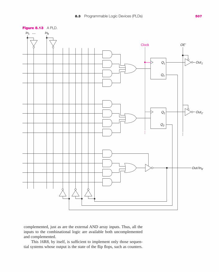
complemented, just as are the external AND array inputs. Thus, all theinputs to the combinational logic are available both uncomplementedand complemented.
This 16R8, by itself, is sufficient to implement only those sequen-tial systems whose output is the state of the flip flops, such as counters.
8.3 Programmable Logic Devices (PLDs) 507
Figure 8.13 A PLD.In1 In8
Q1�
Out1�
Out2�
Out/In8�
Q1
Q2�
Q2
Clock OE�
...
...
...
mar91647_c08_493_542.qxd 11/24/08 10:32 AM Page 507

508 Chapter 8 Solving Larger Sequential Problems
EXAMPLE 8.5
We developed the following equations for the D inputs in Example 7.8:
DA � x�A�B � x�AB� � x�yA � xAB � xy�A�B�
DB � x�yA � AB� � x�B� � y�B�
(There is no point in considering sharing, since the PAL does not permit it.)We can obtain the output equations from the state table (or we could con-struct maps):
F � x�yAB � xyA�B�
G � x�y�AB � xy�A�B�
A block diagram of that PAL, with only the gates that are used included, isshown next. Note that we did not show the output gates for the flip flops.We used five of the eight input lines (including one for a 1 to enable the twooutputs). We used only two of the flip flops. This could be implemented witheither a 16R6 or a 16R4.
A� B� F GA B xy � 00 xy � 01 xy � 10 xy � 11 xy � 00 xy � 01 xy � 10 xy � 11
0 0 0 1 0 1 1 1 0 0 0 0 0 0 0 1 1 00 1 1 0 1 0 0 0 0 0 0 0 0 0 0 0 0 01 0 1 1 1 1 0 1 0 1 0 0 0 0 0 0 0 01 1 0 0 1 1 1 0 1 0 0 1 1 0 0 0 0 0
Those outputs that are not registered (as shown in the bottom of Fig-ure 8.13) are enabled by one of the AND gates (and the PAL has onlyseven terms). If it is not enabled, that pin can be used as an additionalinput (making as many as 12 inputs for the 16R4).
As an example, we will look at the design of the up/down counter fromExample 7.8, where we have added two outputs, F and G, where F indi-cates that the counter is saturated and G indicates that the counter is recy-cling (that is, going from 3 back to 0 or from 0 back to 3). The state table isshown below.
mar91647_c08_493_542.qxd 11/24/08 10:32 AM Page 508

8.3 Programmable Logic Devices (PLDs) 509
1 x y
Q�B�
B�
A�
A�
F
G
Q
D
Q�
Q
D
Clock
The PLDs we have described are useful for relatively smallcircuits—typically no more than a total of 32 inputs and outputs.Although it would theoretically be possible to build them much larger,other approaches are used.
mar91647_c08_493_542.qxd 11/24/08 10:32 AM Page 509

510 Chapter 8 Solving Larger Sequential Problems
A complex programmable logic device (CPLD)* incorporates anarray of PLD-like blocks and a programmable interconnection network.Commercially available CPLDs have as many as a few hundred PLDblocks.
For larger circuits, field programmable gate arrays (FPGA) areused. Rather than containing PALs, FPGAs have as their basic buildingblock a general purpose logic generator (typically three to five variables),with multiplexers and a flip flop. These blocks are connected by a pro-grammable routing network, which also connects to input/output blocks.The logic generator is effectively a lookup table (LUT), often with a flipflop. A three-variable LUT is shown in Figure 8.14, with a flip flop thatmay be bypassed if Control is 0. Each cell can be programmed to a 0 ora 1; thus, any three-variable function can be created.
*For a more complete discussion of CPLDs and FPGAs, see Brown and Vranesic,Fundamentals of Digital Logic with VHDL Design, 3rd ed., McGraw-Hill, 2009.
Figure 8.14 A three-input lookup table.
D
Q
0/1
0/1
0/1
0/1
0/1
0/1
0/1
0/1z y x Control
f
Out
If, for example, the cells are programmed to 0, 0, 0, 1, 0, 0, 1, 1, then thefunction represented is f � x�yz � xyz� � xyz � yz � xy. To illustratethe interconnection network, Figure 8.15 shows an implementation ofthe function
f � x1x2� � x2x3
using two-input LUTs. The brown input/output connectors, connections(X), and LUTs are active. All of the others are inactive. One LUTproduces f1 � x1x2�, the second produces f2 � x2x3, and the third producesf � f1 � f2.
mar91647_c08_493_542.qxd 11/24/08 10:32 AM Page 510

8.4 DESIGN USING ASM DIAGRAMS
As we indicated in Chapter 6, the term state machine, also called finitestate machine or algorithmic state machine (ASM) is the same assequential system. A tool that is a cross between a state diagram and aflow chart is the ASM diagram (sometimes referred to as an ASM chart).We will first describe the basic elements and compare its structure to thatof a state diagram. Then, we will apply this tool to a controller for asmall system of registers (the place where this tool is most useful).
There are three types of blocks in an ASM diagram. The first is thestate box. It is a rectangle, with one entry point and one exit point, asshown in Figure 8.16a.
The name of the state is shown above the box, and the output(s)corresponding to that state is shown in the box. (This is a Moore typeoutput, one that occurs whenever the system is in that state. We will seehow to indicate a Mealy output shortly.) When an output is listed, itindicates that the output is 1; any output not listed is 0.
The second type of box is the decision box, as shown in Figure 8.16b,which allows a two-way branch based on a switching expression.
8.4 Design Using ASM Diagrams 511
Figure 8.15 A section of a programmed FPGA.
0010
x1
x2
x2
x1
x3 f
f1
0001
x2
x3
f2 …
…
……
0111
f1
f2
f
[SP 5]
mar91647_c08_493_542.qxd 11/24/08 10:32 AM Page 511

It has one entry point and two exit points, one corresponding to theexpression equal to 0, the other corresponding to a 1. If more than a two-way branch is needed, the exit of a decision box can go to the entry ofanother decision box.
The third type of box is the conditional output box (Figure 8.16c). Ithas one entry and one exit. It specifies the output that occurs when thatstate transition takes place. (It is the Mealy output.)
An ASM block consists of the state box and all the decision boxesand conditional output boxes connected to it. There is one entry to theblock, but there may be one or more exits; each of these goes to the entryof a state box.
There is no symbol for a merge point; two or more exit paths maygo to the same entry point, as will be seen in some examples below. Atypical ASM block (associated with state A) is shown in Figure 8.17.The output, z, of this system is 1 when the system is in state A andthe input, x, is 1. The system goes to state B when x � 1, and back tostate A when x � 0.
512 Chapter 8 Solving Larger Sequential Problems
Figure 8.17 An ASM block.
z
x0
A
B
1
We will now look at the ASM diagram for the Moore system with anoutput of 1 iff the input has been 1 for at least three consecutive clocks(as first presented in Section 6.1). The state diagram is shown first inFigure 8.18 and then the corresponding ASM diagram.
Figure 8.16a State box.
output
name
Figure 8.16b Decision box.
condition0 1
Figure 8.16c Mealy output box.
output
mar91647_c08_493_542.qxd 11/24/08 10:32 AM Page 512
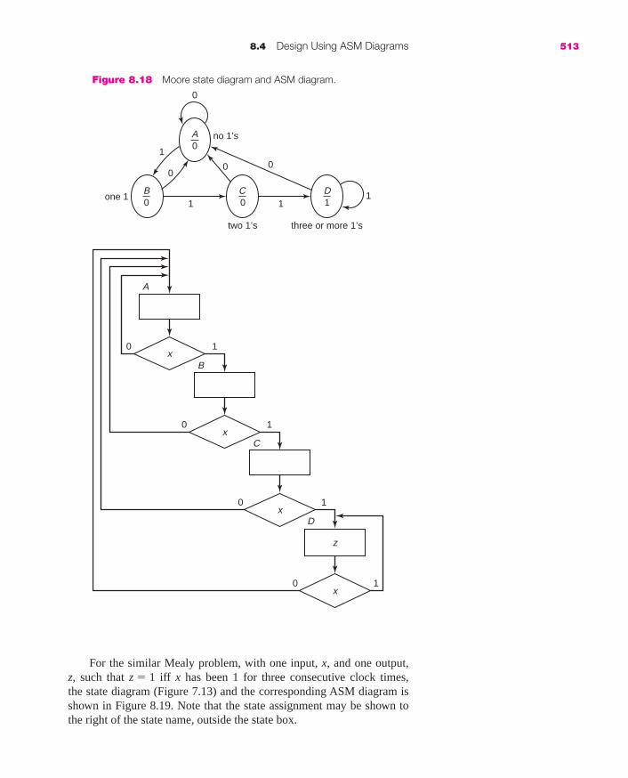
8.4 Design Using ASM Diagrams 513
Figure 8.18 Moore state diagram and ASM diagram.
A0
1
no 1’s
two 1’s three or more 1’s
one 1
00
0
0
B0
C 0 11
D1
1
x
x
x
x
0
0
0
0
A
B
C
D
1
1
1
1
z
For the similar Mealy problem, with one input, x, and one output,z, such that z � 1 iff x has been 1 for three consecutive clock times,the state diagram (Figure 7.13) and the corresponding ASM diagram isshown in Figure 8.19. Note that the state assignment may be shown tothe right of the state name, outside the state box.
mar91647_c08_493_542.qxd 11/24/08 10:32 AM Page 513

514 Chapter 8 Solving Larger Sequential Problems
Figure 8.19 Mealy state diagram and ASM diagram.
0/0
0/0two or more 1's
one 1
no 1’s
0/0
1/0
1/11/0
B
A
Cx
x
0
0
0 1
A
B
C
1
1
10
01
00
z
x
Finally, we will look at the design for a controller for a serial adder. The num-bers are each stored in an 8-bit register (with shifting capability), and theanswer is returned to one of those registers, as shown in the diagram below(a simplified version of this is given in Experiment 24). We will assume thatthe two operands are already loaded into registers A and B.
A signal of 1 on line s indicates that the system is to start the additionprocess. A 1 (for one clock period) on line d indicates that it is done. AnASM diagram for a controller for this system follows. The bits of the registerare numbered 7 (left, most significant) to 0. Bits 0 of the numbers and thecarry (c) are added, and the result is loaded into the left bit (bit 7) of B asboth registers are shifted to the right.
FullAdder
Flip Flop
Registers
...
...
cA
B
EXAMPLE 8.6
mar91647_c08_493_542.qxd 11/24/08 10:32 AM Page 514

This controller can be implemented by a sequential machine with threestates. It requires a 3-bit register, N, and an incrementer to count throughthe eight add/shift steps. This controller goes from state 00 to state 01when s � 1 (and remains in state 00, otherwise). It goes from state 01 to 10when register N contains three 1’s (and returns to state 01, otherwise). Italways goes from state 10 to 00 on the next clock. The design of thesequential circuit is left as an exercise.
8.5 ONE-HOT ENCODING
Up until now, we have encoded states using the minimum number of flipflops. Another approach, particularly simple when designing from anASM diagram, is to use one flip flop for each state. That flip flop is 1 (orhot) and all others are 0 when the system is in that state.
For the Moore system of Figure 8.18, we have four states and wouldthus have four flip flops. If we labeled them A, B, C, and D, we can seeby inspection that
A� � x�(A � B � C � D) � x�
s0
wait
add
1
0 1
done 1 01
0
A <- A[0], A[7:1]B <- A[0]�B [0]�c, B [7:1]c <- carryN <- N�1
0 0
N � 7
c <- 0N <- 0
d
8.5 One-Hot Encoding 515
[SP 6; EX 7, 8]
mar91647_c08_493_542.qxd 11/24/08 10:32 AM Page 515

(since one of the state variables must be 1).
B� � x A
(since the condition box indicates that we go to state B when x � 1)
C� � x B
D� � x(C � D)
This produces very simple combinational logic for the next state (althoughthe savings there is typically not adequate to make up for the cost of extraflip flops).
The output is 1 only when in state D; thus the output equation is
z � D
This approach is sometimes used in designing large controllers, wheremost states produce an output signal. As in the example above, the out-put signal comes directly from a flip flop, rather than from combinationallogic that decodes the state.
8.6 VERILOG FOR SEQUENTIAL SYSTEMS*
In Section 5.7.1, we introduced Verilog constructs for combinational sys-tems. Here, we will give examples of the use of Verilog for sequentialsystems.
We will now look at the structural model for a trailing-edge trig-gered D flip flop with an active low input, CLR� in Figure 8.20.
516 Chapter 8 Solving Larger Sequential Problems
Figure 8.20 Structural model of a D flip flop.
module D_ff (q, ck, D, CLR);input ck, D, CLR;output q;reg q;always @ (negedge ck or negedge CLR)
beginif (!CLR)
q <= 0;else
q <= D;end
endmodule
*For a detailed discussion of Verilog, see Brown and Vranesic, Fundamentals of DigitalLogic with Verilog Design, 2nd ed., McGraw-Hill, 2008, or for VHDL, see Brown andVranesic, Fundamentals of Digital Logic with VHDL Design, 3rd ed., McGraw-Hill, 2009.
mar91647_c08_493_542.qxd 11/24/08 10:32 AM Page 516

8.6 Verilog for Sequential Systems 517
Note that q is referred to as a register (reg) rather than a wire, sinceit is storage. The symbol @ indicates the time when the following stepsare executed. Only on the trailing edge (negedge) of the clock or theCLR input will anything happen. The symbol ! indicates not, and thearrowed equal (<=) is used to indicate time dependence. In the combina-tional models, an equal sign (=) was used since it did not matter in whatorder things happened.
We can use the flip flop we just described to build an 8-bit trailing-edge triggered shift register (shift right), as shown in Figure 8.21a.
Figure 8.21a Shift register using flip flop module.
module shift (Q, x, ck, CLR);input x, clock, CLR;output [7:0]Q;wire [7:0]Q;D_ff Stage 7 (Q[7], x, ck, CLR);D_ff Stage 6 (Q[6], Q[7], ck, CLR);D_ff Stage 5 (Q[5], Q[6], ck, CLR);D_ff Stage 4 (Q[4], Q[5], ck, CLR);D_ff Stage 3 (Q[3], Q[4], ck, CLR);D_ff Stage 2 (Q[2], Q[3], ck, CLR);D_ff Stage 1 (Q[1], Q[2], ck, CLR);D_ff Stage 0 (Q[0], Q[1], ck, CLR);
endmodule
Figure 8.21b Single module shifter.
module shift (Q, x, ck, CLR);input x, clock, CLR;output [7:0]Q;wire [7:0]Q;reg [7:0]Q;
always (@ negedge ck)begin
Q[0] <= Q[1];Q[1] <= Q[2];Q[2] <= Q[3];Q[3] <= Q[4];Q[4] <= Q[5];Q[5] <= Q[6];Q[6] <= Q[7];Q[7] <= x;
endendmodule
Another approach is to define the shift register in a single module.
mar91647_c08_493_542.qxd 11/24/08 10:32 AM Page 517
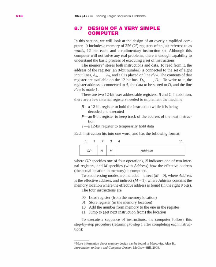
518 Chapter 8 Solving Larger Sequential Problems
*More information about memory design can be found in Marcovitz, Alan B.,Introduction to Logic and Computer Design, McGraw-Hill, 2008.
8.7 DESIGN OF A VERY SIMPLECOMPUTER
In this section, we will look at the design of an overly simplified com-puter. It includes a memory of 256 (28) registers often just referred to aswords, 12 bits each, and a rudimentary instruction set. Although thiscomputer will not solve any real problems, there is enough capability tounderstand the basic process of executing a set of instructions.
The memory* stores both instructions and data. To read from it, theaddress of the register (an 8-bit number) is connected to the set of eightinput lines, A0, . . . , A7, and a 0 is placed on line r�/w. The contents of thatregister are available on the 12-bit bus, D0, . . . , D11. To write to it, theregister address is connected to A, the data to be stored to D, and the liner�/w is made 1.
There are two 12-bit user addressable registers, B and C. In addition,there are a few internal registers needed to implement the machine:
R—a 12-bit register to hold the instruction while it is beingdecoded and executed
P—an 8-bit register to keep track of the address of the next instruc-tion
T—a 12-bit register to temporarily hold data
Each instruction fits into one word, and has the following format:
AddressN MOP
0 1 2 3 4 11
where OP specifies one of four operations, N indicates one of two inter-nal registers, and M specifies (with Address) how the effective address(the actual location in memory) is computed.
Two addressing modes are included—direct (M = 0), where Addressis the effective address, and indirect (M = 1), where Address contains thememory location where the effective address is found (in the right 8 bits).
The four instructions are
00 Load register (from the memory location)01 Store register (in the memory location)10 Add the number from memory to the one in the register11 Jump to (get next instruction from) the location
To execute a sequence of instructions, the computer follows thisstep-by-step procedure (returning to step 1 after completing each instruc-tion):
mar91647_c08_493_542.qxd 11/24/08 10:32 AM Page 518

1. Send the address of the instruction (from the Program Counter, Pin what follows) to memory to fetch the instruction. Save that wordin an internal register of the CPU, sometimes called the InstructionRegister, I, in the description that follows.
2. Update the Program Counter so that it points to the (first word ofthe) next instruction.
3. Decode the instruction, that is, determine what operation is to beperformed and what operands, if any, are needed.
4. Obtain the operands. Some may be in registers and others inmemory. In the latter case, the address may need to be computedand the data fetched from memory into a CPU register.
5. Execute the instruction, that is, do the computation (if any)required.
6. Store the result, if any, either in memory or in a register. (For jumpinstructions, the result may be the address of the next instruction tobe stored in the Program Counter.)
An ASM diagram for the controller of this computer is shown inFigure 8.22. Rather than showing output boxes, we have labeled eachstate box with the steps that are to be performed. In the first step, the pro-gram counter (which contains the address of the instruction about to beexecuted) is connected to the address input and the instruction is readinto I. If I3 is 1, this is indirect addressing, and the right 8 bits of I arereplaced by the contents of the memory location. The Program Counter,P, is incremented to point to the next instruction, and, based on I1, theflow branches. To the left, we read data from memory into the temporaryregister, T. For Load, it is moved to the appropriate register; for Add, T isadded* to either register B or C. For the right branch, P is changed to theaddress portion of I for a jump. For store, the appropriate register is con-nected to D, the address to A, and r�/w is made 1 (to write the data intomemory).
This controller implies that the bus D has inputs from memory andregisters B and C. Its contents can be clocked into registers I (or the right8 bits of I) and T. There is a 12-bit adder, with neither a carry-in nor acarry-out, that takes one input from T and the other either from B or C(implying a multiplexer on the second input). The internal transfersimplied are from the right 8 bits of I to P, and from T to B and C.
The state boxes in the ASM diagram have been numbered, and wethen implemented the controller using a one-hot design (where each statecorresponds to a 1 in just one of the flip flops) in Figure 8.23. The clockinputs have not been connected to the clock in that figure to make it morereadable.
8.7 Design of a Very Simple Computer 519
*We have used the notation ++ to indicate addition (as opposed to OR).
mar91647_c08_493_542.qxd 11/24/08 10:32 AM Page 519

8.8 OTHER COMPLEX EXAMPLES
As the first example, consider the design of the following system:
The system keeps track of how many consecutive 1 inputs occur on inputline x and then, starting at the first time that the input x is 0, it outputs online z that same number of 1’s at consecutive clocks (z is 0 at all othertimes).
520 Chapter 8 Solving Larger Sequential Problems
Figure 8.22 ASM diagram for very simple computer.
1
1
1
10
01 1 1
0
0
11
0
0
4
2
3
0
1
1098765
A = P
r �/w = 0I <- D
R3
R1
R0
R2R2
R0
R2
IncrementP
P <- I � 4:11�
B <-T C <-T B <-B ++ T C <-C ++ TA = I �4:11�
r �/w = 1D = C
A = I �4:11�r �/w = 1D = B
A = I �4:11� r �/w = 1
T <- D
A = I �4:11�r �/w = 0
I �4: 11� <- D �4:11�
mar91647_c08_493_542.qxd 11/24/08 10:32 AM Page 520

8.8 Other Complex Examples 521
A sample timing trace of the input and output of such a system is shownin Trace 8.2.
We will first assume that the available components are AND, OR, andNOT gates, a JK flip flop and a 74191 up/down counter with four out-puts, labeled D, C, B, A (with D the high-order output). We will use thecounter to count the number of consecutive 1’s (counting up) and thencount down to 0 as the 1’s are output.
We will first look at the simplest solution and then examine theassumptions that must be made for this to be valid. We will then addcircuitry so as to make the system work for a more general case. Thecircuit of Figure 8.24 is our first attempt at a solution. No clear wasprovided. Once the system produces its last 1 output, the counter willbe left with 0 in it; so there is no need to clear it. When x is 1, the D/U�is set to 0, and the counter is enabled; thus, it counts up. When x returnsto 0, it will count down, as long as it is enabled, that is, as long as there
Trace 8.2
x 0 0 0 1 0 0 0 0 1 1 1 1 0 0 0 0 0 0 0 1 1 0 0 0z 0 0 0 0 1 0 0 0 0 0 0 0 1 1 1 1 0 0 0 0 0 1 1 0
R3
R1
R0
R2 R2
R0
1
2
3
9
10
11
4
5
6
7
8
Figure 8.23 One hot design of controller.
mar91647_c08_493_542.qxd 11/24/08 10:32 AM Page 521

is a nonzero value in the counter. The output is 1 when x is 0 and thereis a nonzero count. This solution works only if the count never exceeds15, since on the 16th consecutive 1 input, the counter goes back to 0.If a larger number were required, we would need one or more addi-tional counters so as to be able to count higher than 15. An alternativeto that would be to limit the output to a maximum of 15 1’s, even ifthe input included more than 15 consecutive 1’s. In that case, we woulddisable the counter when we reached 15, if x remains 1. That wouldrequire the circuit of Figure 8.25.
522 Chapter 8 Solving Larger Sequential Problems
Figure 8.25 Example with maximum of 16 outputs of 1.
D C B A
END/U�
x
Clock
z
Figure 8.24 A simple solution with a counter.
D C B A
END/U �
x
Clock
z
mar91647_c08_493_542.qxd 11/24/08 10:32 AM Page 522

8.8 Other Complex Examples 523
*Since the counter is not enabled, it does not matter whether it is set to count up or down.
†If there is only one 1, that will cause the counter to increase to 1, but Q will not be set atthe next clock time, since that is the last time the output is to be 1. The condition to set Qis just that the count is between 2 and 15, which yields, from the map, D � C � B.‡When it is counting down (and the output is 1), the input is ignored; it does not matter.
Now the counter is not enabled when the count is 15 (1111) and xis 1. Thus, if there are a large number of consecutive 1’s, it will countto 15 and stop until x goes to 0; then it will count down, outputtingfifteen 1’s.
The other unstated assumption that we made was that x remains 0until the 1 outputs are completed. That was the case in the sample trace.If that is not true, the counter will start counting up again as soon as xreturns to 1 and the output will be 0. Assuming that we want to ignore theinput until the 1 outputs are completed, we need a flip flop, Q, to keeptrack of when the system is counting down and we should ignore x. Wemust then consider the following possibilities.
x � 0 Q � 0 count � 0 EN � 0 z � 0 D/U� � X *
x � 0 Q � 0 count � 1† EN � 1 z � 1 D/U� � 1
x � 0 Q � 0 count � 1 EN � 1 z � 1 D/U� � 1 Q �– 1
x � 1 Q � 0 count 15 EN � 1 z � 0 D/U� � 0
x � 1 Q � 0 count � 15 EN � 0 z � 0 D/U� � Xx � X ‡ Q � 1 count � 1 EN � 1 z � 1 D/U� � 1
x � X Q � 1 count � 1 EN � 1 z � 1 D/U� � 1 Q �– 0
Flip flop Q will be turned on when x is 0 and the count is not 0 or 1, andit will be turned off when it is 1 and the output gets down to 1. Thus,
J � x�(D � C � B) K � D�C�B�A
The output is 1 when Q is 1 or when x is 0 and Q is 0 but the count is not0. Thus,
z � Q � x�Q�(D � C � B � A) � Q � x�(D � C � B � A)
The counter is enabled when x � 1 and the count is not at 15 (as in thelast example, to allow for more than 15 consecutive 1 inputs) or whenz � 1. Thus,
EN � x(ABCD)� � z
mar91647_c08_493_542.qxd 11/24/08 10:32 AM Page 523

Finally,
D/U� � Q � x�(D � C � B � A)
the same as z, since at the only places where they differ, D/U� is a don’tcare (since the counter is not enabled).
We will now look at the same example, utilizing shift registersinstead of a counter. We need some right/left shift registers (more than 1if we are to allow more than four consecutive 1 outputs). If we set thelimit at 12, we could use three 74194 shift registers. They would be con-nected as shown in Figure 8.26, where the parallel inputs are not shown,since they are not used.
524 Chapter 8 Solving Larger Sequential Problems
Figure 8.26 Circuit using three right/left shift registers.
S1
q4
LS
q1
S0CLR �
RSS1
q4
LS
q1
S0CLR �
RSS1
q4
LS
x
z
q1
S0CLR �
RS
CLK
1 0
The three shift registers are connected to form one 12-bit shift register.When x � 1, S0 � 1, and S1 � 0, making the registers shift right. A 1 isshifted into the leftmost bit. When x � 0, the register shifts left, loading0’s from the right. After the input has been 0 for several clocks (or if theshift register is cleared), all bits will be 0. The output is 1 whenever thereis a 1 in the left bit of the shift register and x is 0. Note that if there aremore than 12 consecutive 1 inputs, the shift register will contain all 1’s.When the input goes to 0, the output will be 1 for 12 clock times. Thus,this solution handles the situation where there are more 1 inputs than theregister can hold (similar to the second counter design).
If the input could go to 1 again while the output is still 1, we need anextra flip flop, Q, here, as well. This flip flop is set (J � 1) when x � 0and q2 of the left shift register is 1 (indicating that there have been at leasttwo 1’s). It is cleared (K � 1) when q2 is 0 (indicating that there are nomore than one more 1 to be output). S0 becomes xQ� and S1 becomesx� � Q.
mar91647_c08_493_542.qxd 11/24/08 10:32 AM Page 524

Design a counter that goes through the following sequence of 16 states
1 2 4 7 11 0 6 13 5 14 8 3 15 12 10 9, and repeat
It does not matter where it starts. For the combinational logic, thereare packages of NAND gates (7400, 7404, 7410, 7420, and 7430) avail-able at 50¢ each. We will consider two alternative designs and com-pare them. The first uses four JK flip flops at a total cost of $2.00. Thesecond uses a 4-bit synchronous counter (such as the 74161) and a com-binational decoder block. This block takes the output of the counter thatgoes 0, 1, 2, 3, 4, . . . and translates the 0 to 1, the 1 to 2, the 2 to 4, andso forth.
First, we will design the counter using JK flip flops. The state table isshown below.
8.8 Other Complex Examples 525
D C B A D� C� B� A�
0 0 0 0 0 1 1 00 0 0 1 0 0 1 00 0 1 0 0 1 0 00 0 1 1 1 1 1 10 1 0 0 0 1 1 10 1 0 1 1 1 1 00 1 1 0 1 1 0 10 1 1 1 1 0 1 11 0 0 0 0 0 1 11 0 0 1 0 0 0 11 0 1 0 1 0 0 11 0 1 1 0 0 0 01 1 0 0 1 0 1 01 1 0 1 0 1 0 11 1 1 0 1 0 0 01 1 1 1 1 1 0 0
EXAMPLE 8.7
We can map these functions and use the quick method to find the JK flipflop input equations, as shown next.
00 01 11 10
00
01
11
10
D CB A
1
1
1
1
111
1
00 01 11 10
00
01
11
10
D CB A
1
1111
1
11
00 01 11 10
00
01
11
10
D CB A
1
111
1 11
1
00 01 11 10
00
01
11
10
D CB A
11
1
1
1
1
1
1
ABC ★D★ ★★
mar91647_c08_493_542.qxd 11/24/08 10:32 AM Page 525

JD � CA � CB � BA KD � C�B� � C�A � B�A
JC � D�A� � D�B KC � DA� � D�BA
JB � D� � A� KB � D � A�
JA � D�C � DC� KC � D�B� � CB� � DC�B
This would require 18 two-input gates and 5 three-input gates or a total of7 integrated circuit packages at 50¢ each. Thus, the total cost is $5.50.
For the other approach, we construct the following truth table for thedecoder block:
The output maps are then shown below.
526 Chapter 8 Solving Larger Sequential Problems
D C B A W X Y Z
0 0 0 0 0 0 0 10 0 0 1 0 0 1 00 0 1 0 0 1 0 00 0 1 1 0 1 1 10 1 0 0 1 0 1 10 1 0 1 0 0 0 00 1 1 0 0 1 1 00 1 1 1 1 1 0 11 0 0 0 0 1 0 11 0 0 1 1 1 1 01 0 1 0 1 0 0 01 0 1 1 0 0 1 11 1 0 0 1 1 1 11 1 0 1 1 1 0 01 1 1 0 1 0 1 01 1 1 1 1 0 0 1
00 01 11 10
00
01
11
10
D CB A
1
W
1
11
1 1
1 1
00 01 11 10
00
01
11
10
D CB A
1
X
1
1 1
11
1 1
00 01 11 10
00
01
11
10
D CB A
1
Y
1
11
11
11
00 01 11 10
00
01
11
10
D CB A
Z
1 111
11 1 1
W � CB�A� � DB�A � CBA � DBA�
X � DB� � D�B
Y � C�A � CA�
Z � B�A� � BA
This requires 9 two-input gates, 4 three-input gates, and 1 four-input gate.In addition, we need four NOT gates (a 7404 package), since only theuncomplemented outputs from the counter (D, C, B, and A) are available.
mar91647_c08_493_542.qxd 11/24/08 10:32 AM Page 526

8.9 Solved Problems 527
[SP 5, 6; EX 6, 9, 10, 11, 12, 13, 14, 15;LAB]
The total required is six packages. Thus, this approach costs $3.00 plus thecost of the counter and is less expensive if the counter costs less than$2.50.
It is interesting to note that if we built the counter using four JK flipflops, we would only need to create the functions BA and CBA. That wouldrequire just two NOT gates, since (BA)� and (CBA)� are used in W and Z.Thus, we end up with only six packages and a total cost of $5.00, which isless expensive than the first solution. This solution is best if the countercosts more than $2.00.
x x
Clock
A B C D E F G H
z
(We really only needed a 5-bit shift register, but it is easier andless expensive to use an 8-bit one than to build a 5-bit one withflip flops.)
2. Design a Moore circuit, using a 74164 shift register and AND,OR, and NOT gates to produce a 1 output for every eighth 1input (not necessarily consecutive). We are not concerned aboutwhen the first output comes, as long as there is a 1 for everyeight 1 inputs thereafter.
We will input a 1 to the shift register, clocking it only when theinput is 1. When a 1 reaches the last flip flop, H, the shift registerwill be cleared. We can take the output from G (or from any of the
8.9 SOLVED PROBLEMS
1. Design a Mealy system using a 74164 shift register and what-ever gates are needed to produce an output of 1 when the lastsix inputs have been 1, and 0 otherwise.
The shift register stores the previous eight inputs; we only needthe five most recent ones. The circuit is shown below.
mar91647_c08_493_542.qxd 11/24/08 10:32 AM Page 527

528 Chapter 8 Solving Larger Sequential Problems
The counter will be reset whenever the input is 0 and will beallowed to count when the input is 1 until the count reaches 11.At that point, if the input is 1, there will be a 1 output. A blockdiagram is shown below.
Note that the counter is enabled whenever x � 1 and the outputis not already 1; that keeps it from counting beyond 11.
4. Design a system such that when the input, x, goes to 1 duringone clock period, the output, z, will be the next eight consecutiveclocks. z will be 0 at all other times. Assume that x remains 0throughout the period of nonzero output. Show the blockdiagram.
D C B A
z
ENP
Clock
ENTCLR �
x
OV 74161
LD �
1
1
x
x
Clock
A B C D E F G
z
H
CLR�
3. Design a Mealy system, using a 74161 counter and AND, OR,and NOT gates that produces a 1 output when the input has been1 for at least 12 consecutive clock times.
first seven flip flops); it goes to 1 on the seventh 1 input and iscleared shortly after the eighth. A block diagram is as follows:
mar91647_c08_493_542.qxd 11/24/08 10:32 AM Page 528

Example:
8.9 Solved Problems 529
Clock
x
z
z
or
Use AND, OR, and NOT gates plus either
a. a trailing-edge triggered 8-bit serial-in, serial-out shiftregister with a static, active low clear, CLR�, or
b. a trailing-edge triggered 4-bit counter with a static, activelow clear, CLR�.
Assume either that this has been running for a while or that wedon’t look at the output before the first time x � 1.
a. We will use x to clear the shift register and will clock a 1 intothe leftmost bit at each clock time thereafter. The output willbe taken from the right bit; when it is 0, there will be a clockpulse.
This circuit produces the second timing picture, since the firstoutput occurs during the time x is 1. Note that this only usesthe serial output; if H� is available, we do not need the outputNOT gate.
b. For the counter design, we will use x to clear the counter andlet it count as long as the count is less than 8 (that is, D � 0).Either of the following circuits could be used.
1
x
x
Clock
H
ck CLR�
z
mar91647_c08_493_542.qxd 11/24/08 10:32 AM Page 529

530 Chapter 8 Solving Larger Sequential Problems
In both cases, the timing is that of the second drawing.
5. Design a system that counts up from 1 to 6 (and repeat) wheninput x is 0 and down from 6 to 1 when x � 1 and displays theresults on a die. The die has seven lights (as shown in thediagram below).
A 1 for each segment (a, b, c, d, e, f, g) indicates that it is lit; a 0that it is not. The arrangement for the six numbers on a die areshown below, where the darkened circles are to be lit.
a
b
c
e
fd
g
D C B A
z
x
ENP
Clock
ENTCLR �
OV
LD �
1 1 1
D C B A
x
ENP
Clock
ENTCLR �
OV
LD �
z1 1
1 2 3 4 5 6
Design the counter, using three D flip flops to count from 1(001) to 6 (110) and repeat. Then, design a decoder/driver thattakes the outputs from the counter and produces the sevensignals (a, b, c, d, e, f, g) to drive the display. Use a 16R4 PLD.(That works since there are really only four distinct outputs; aand g, b and f, and c and e are always the same.)
Labeling the flip flops F, G, and H, we get the followingtruth table for the system. There are only eight rows for thedisplay inputs, since they do not depend on x.
mar91647_c08_493_542.qxd 11/24/08 10:32 AM Page 530
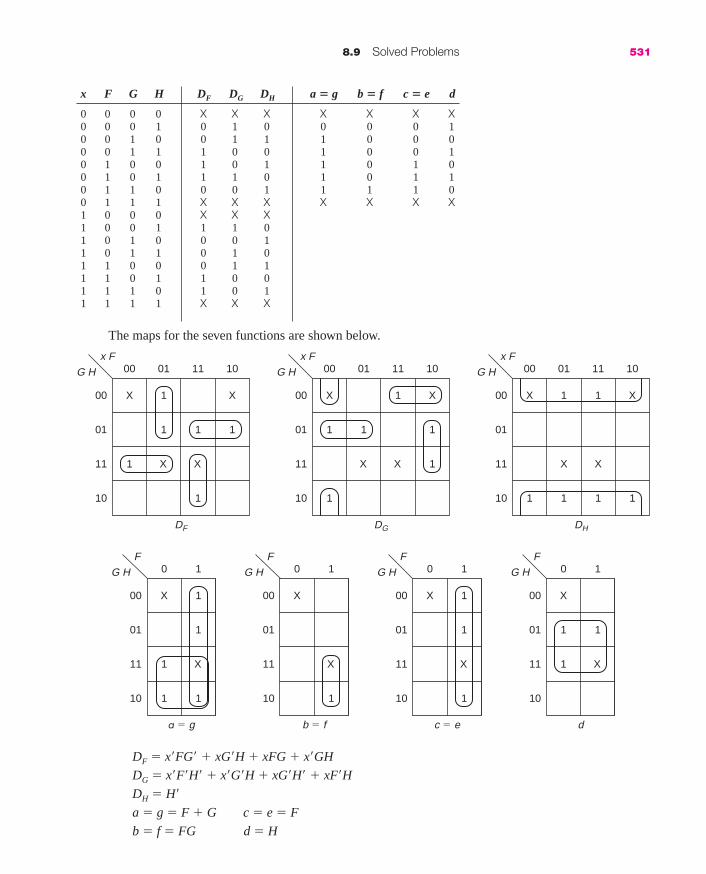
8.9 Solved Problems 531
The maps for the seven functions are shown below.
00 01 11 10
00
01
11
10
x F
DF
G H
X X
1
1
XX 1
111
00 01 11 10
00
01
11
10
x F
DG
G H
X X
1
1
XX 1
11 1
00 01 11 10
00
01
11
10
x F
DH
G H
X X
1 1 1 1
XX 11
0 1
00
01
11
10
F
a � g
G H
X1
1 1
X 1
1
0 1
00
01
11
10
F
b � f
G H
X
1
X
0 1
00
01
11
10
F
c � e
G H
X
1
1
1X
0 1
00
01
11
10
F
d
G H
X1
11
X
DF � x�FG� � xG�H � xFG � x�GH
DG � x�F�H� � x�G�H � xG�H� � xF�H
DH � H�
a � g � F � G c � e � F
b � f � FG d � H
x F G H DF DG DH a � g b � f c � e d
0 0 0 0 X X X X X X X0 0 0 1 0 1 0 0 0 0 10 0 1 0 0 1 1 1 0 0 00 0 1 1 1 0 0 1 0 0 10 1 0 0 1 0 1 1 0 1 00 1 0 1 1 1 0 1 0 1 10 1 1 0 0 0 1 1 1 1 00 1 1 1 X X X X X X X1 0 0 0 X X X1 0 0 1 1 1 01 0 1 0 0 0 11 0 1 1 0 1 01 1 0 0 0 1 11 1 0 1 1 0 01 1 1 0 1 0 11 1 1 1 X X X
mar91647_c08_493_542.qxd 11/24/08 10:32 AM Page 531
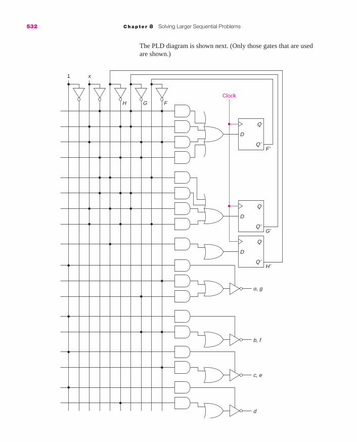
532 Chapter 8 Solving Larger Sequential Problems
1 x
H G F
Q�F �
G�
H�
a, g
b, f
c, e
d
Q
D
Q�
Q
D
Q�
Q
D
Clock
The PLD diagram is shown next. (Only those gates that are usedare shown.)
mar91647_c08_493_542.qxd 11/24/08 10:32 AM Page 532

6. We are designing a rather rudimentary alarm system. The firstpart of the system includes a flip flop A that is 1 if the alarm isset (armed) and 0 if it is not, and a keypad (with 10 keys and 4 output lines). It produces an output of all 1’s if no key is pushedor 0000 to 1001 if one of keys 0 to 9 are pushed. (You mayassume that two keys are never pushed at the same time and thatthe keypad never produces one of the other five combinations.)
To set or clear the alarm, a 3-digit combination must beentered. Hidden away in the control box is a set of three10-position switches (that contains the 3-digit alarm code). Theswitches each produce a 4-bit number, R1:4, S1:4, and T1:4. Asone pushes the buttons to enter the alarm code, the first digitwill appear on the keypad output for several clock periods,followed by a hexadecimal F (indicating that no key is pushed)for several more clock periods, followed by the second digit,and so on. We must design a system that watches the keypadand, if the right code is received, complements A. (Note: Likemany alarms, the same code is used to arm the alarm, that is,put a 1 in A, as to disarm it.) Assume that there is at least oneclock period when no key is pushed between digits. However, ifanother key is not depressed within 100 clocks, the system goesback to looking for the first digit.
The second part of the system is used to sound the alarm.There is an input signal, D, indicating that a door is open (1) orclosed (0) and an output, N, indicating that the alarm is sounded(1) or not (0). (Of course, A is also an input to this part of thesystem.) When the alarm is first armed, the door must be closedwithin 1000 clock pulses or the alarm will sound. (Note that thisgives the user the chance to set the alarm and go out without thealarm sounding.) Also, if the alarm has been armed for morethan 1000 clock periods and the door is opened, the alarm willsound if it is not disarmed within 1000 clock periods.
Design both parts of this system. Available componentsinclude trailing-edge triggered JK flip flops, synchronous 4-bitbinary or decimal counters, and whatever gates that are needed.Show a modular diagram that shows various parts, also adetailed block diagram or the equations for each part, and anASM diagram for the first part.
One approach to the first part uses the following set of states:
1. Waiting for first input digit.
2. Have first input digit, waiting for key to be released.
3. Nothing pushed, but have first digit—waiting for second.
4. Have first two input digits, waiting for key to be released.
5. Nothing pushed, have two digits—waiting for third.
6. Have third input digit, waiting for key to be released.
8.9 Solved Problems 533
mar91647_c08_493_542.qxd 11/24/08 10:32 AM Page 533

An ASM diagram, ignoring the 100 clock timeout, is shownbelow.
534 Chapter 8 Solving Larger Sequential Problems
0 1
1 0
0
0
0
0
idle
G
G
0 0 1
first 0 1 0
H
second 1 0 0
F
M
wait2 1 0 1
1F
1
1
1
1
10M
third 110
A <- A�
H
wait 0 1 1
mar91647_c08_493_542.qxd 11/24/08 10:32 AM Page 534

If we call the inputs from the keyboard X1:4, then
Nothing pushed � X1X2X3X4 � F
First Digit � (X1 � R1)�(X2 � R2)�(X3 � R3)�(X4 � R4)� � G
Second digit � (X1 � S1)�(X2 � S2)�(X3 � S3)�(X4 � S4)� � H
Third digit � (X1 � T1)�(X2 � T2)�(X3 � T3)�(X4 � T4)� � M
This is a seven-variable problem—the three states q1, q2,and q3, and the functions produced by the inputs, F, G, H, andM. We will code the states in binary (for example, 3 will be011). We will then produce a table in binary, separating thethree flip flop next state sections.
8.9 Solved Problems 535
q1� q2
� q3�
q1 q2 q3 F G H M # F G H M # F G H M #
0 0 0 X X X X X X X X X X X X X X X0 0 1 0 0 0 0 0 0 1 0 0 0 1 0 1 1 10 1 0 0 0 X X X 1 1 X X X 1 0 X X X0 1 1 0 0 1 0 0 1 0 0 0 0 1 1 0 1 11 0 0 1 X 1 X X 0 X 0 X X 1 X 0 X X1 0 1 1 0 0 1 0 0 0 0 1 0 1 1 1 0 11 1 0 0 X X 1 X 0 X X 1 X 1 X X 0 X1 1 1 X X X X X X X X X X X X X X X
where # � F�G�H�M�. Note, only one of F, G, H, or M can be 1.We found expressions for the next state by considering one
column of the table at a time. Although this might not beminimum, it is close.
q1� � Fq1q�2 � H(q2 � q�3) � Mq1
q2� � Fq�1q2 � G(q�1q�2 � q�3) � Mq1
q3� � F � G(q1 � q2q3) � H(q�1q�2 � q1q3) � Mq�1
� F�G�H�M�
The control flip flop, A, is complemented when this controllergoes from state 5 to 6, that is, on q1q�2q3M. The one thing thathas been omitted so far is the time out. A base 100 counter isbuilt with two decade counters. It is cleared when going fromstate 2 to 3 or from 4 to 5 and is enabled whenever thecontroller is in state 2 or 4. It uses the static clear and presetinputs of the controller flip flops to set the controller to state 1as the counter rolls over, that is, goes from 99 to 00.
Next we will design the alarm control. When A goes to 1,a three-digit decade counter will be cleared. When that reaches1000, a second flip flop, B, will be set. When B is set and D
mar91647_c08_493_542.qxd 11/24/08 10:32 AM Page 535

In this diagram, all of the clock inputs are connected to thesystem clock (but not shown to simplify the diagram). Thetwo counters are base 1000 (that is, three decade counterscascaded); all inputs are assumed to be active high. When Agoes to 1, the first counter is cleared. Flip flop B is 0, since it iscleared whenever A has been 0. It will be set when the counterreaches 1000. However, the alarm will be sounded if the door isstill open (first counter overflows and door is open). The alarmflip flop (N) remains set until the code is entered to clear A.The E flip flop is used to produce a clear signal for the secondcounter when the door is first opened. That counter is enabledwhen the door is open and B � 1. The alarm will sound if ithas not been disarmed (causing A and B to go to 0) within1000 clocks.
536 Chapter 8 Solving Larger Sequential Problems
CLR
EN
OV
Counter
CLR
EN OV
Counter
J
A
K
A�
q1
q2� q3
M
J
D
K
E �
J B
K B�
J N
K N �
goes to 1, we will start to count to 1000 again. If, by the timethe counter gets to 1000, A does not go to 0, the alarm willsound; flip flop N will go to 1. Both B and N are cleared whenA goes to 0. A diagram of the system is shown below.
mar91647_c08_493_542.qxd 11/24/08 10:32 AM Page 536

8.10 EXERCISES1. Using a 74164 shift register, design a Mealy system that produces
an output of 1 when the last nine inputs were 0.
2. Using two 74164 shift registers, design a Moore system whoseoutput is 1 when there have been exactly six 1’s followed byexactly eight 0 inputs.
3. Design a system using a counter that produces a 1 output when theinput has been 1 for eight or more consecutive clock times.
a. Use a counter with a clocked active low clear and no enableinput.
b. Use a counter with a static active low clear and an active highenable.
�4. Design a system that has an output of 1 when the input has been0 for exactly seven clock times. In addition to combinational logicblocks, one of the following is available:
a. A 4-bit counter
b. An 8-bit shift register
5. Design a sequential system that has a clock pulse input andproduces a pulse that is coincident with every 25th clock pulse.(We do not care about initializing the system.)
The only available components are
1. AND gates (any number of inputs)
2. Inverters (NOT gates)
3. Two base 16-counters (as described below)
The counter is trailing-edge triggered. It has four outputs—D(high-order bit), C, B, and A. It has a clock input and an active lowstatic Clear� input. There is also an active low static Load� input,along with data input lines, IND, INC, INB, and INA. (Assume thatClear� and Load� are never both 0 at the same time. When either is0, it overrides the clock.)
a. Design a system using these components that uses the Clear�input, but not the Load� input.
b. Design a system using these components that uses the Load�input, but not the Clear� input.
6. Design a system using
a. a 74190
b. a 74192
plus whatever other logic that is needed (including a flip flop) to gothrough the sequence
0 1 2 3 4 5 6 7 8 9 8 7 6 5 4 3 2 1 (0 1) and repeat
7. Implement the controller for the system of Example 8.6 usingD flip flops and NAND gates.
8.10 Exercises 537
EX
ER
CIS
ES
mar91647_c08_493_542.qxd 11/24/08 10:32 AM Page 537

�8. Show the ASM diagram for the controller of a system that has a16-bit register, A, and a 4-bit register, N. When a signal of 1appears on input line s, the register A is shifted right the number ofplaces (0 to 15) as specified by N (with 0’s put in the left bits). Theregister A can be shifted only one place at a time. The register Ncan be decremented (decreased by 1). When shifting is complete, a1 is to appear on output line d for two clock periods.
�9. Design a system that consists of three components, a counter, adisplay driver, and a seven-segment display, as shown below.
a. Design the counter using four JK flip flops, A, B, C, and D,and a minimum number of NOR gates. The counter is binarycoded decimal, using 2421 code (as described in Table 1.7)and is to go through the sequence:
0 3 6 9 2 5 8 1 4 7 and repeat
Thus, the counter sequences 0000, 0011, 1100, 1111, 0010,and so on. After completing the design of this counter, draw astate graph. Make sure that it shows what happens if thecounter is turned on and comes up in one of the unused states(for example, 0101).
b. The outputs of the counter are inputs to the display driver. It isjust a four-input, seven-output combinational circuit. If one ofthe unused codes turns up (for example, the counter is turnedon and ABCD � 0111), the display should be blank (that is,all seven inputs should be 0). Find a near minimum sum ofproducts implementation of X1, X2, X3, X4, X5, X6, and X7.(Use the versions of 6, 7, and 9 without the extra segment lit.)(There is a solution with 17 gates and 56 inputs.)
10. We already have a decimal counter that sequences
0000 0001 0010 0011 0100 0101 0110 0111 1000 1001 and repeat
It has flip flops W, X, Y, and Z. We still want the display to cyclethrough 0, 3, 6, 9, 2, 5, 8, 1, 4, 7, and repeat (as in Exercise 9).Accomplish this by designing another box to go between thecounter and the display driver of Exercise 9b. Note that this means,for example, that when the counter has WXYZ � 0010, the displayis to be 6 and thus ABCD � 1100 (6 in 2421 code). Implement thisbox with a PLA with four inputs and four outputs.
DisplayDriver
Counter
ABCDX1 : X 7
538 Chapter 8 Solving Larger Sequential Problems
EX
ER
CIS
ES
mar91647_c08_493_542.qxd 11/24/08 10:32 AM Page 538

11. Show a block diagram of a system whose output, z, is 1 if and onlyif at least two of the latest three inputs (including the present one)are 0. There is no need to show a state table or state diagram. Anykind of flip flops and gates may be used.
12. Design a sequential system (a counter) with one input line, x, andthree flip flops, A, B, and C. When x � 0, the system sequencesthrough the states (0, 1, 2, 3, 4), 0, . . . and when x � 1, the systemsequences through the states (2, 3, 4, 5, 6, 7), 2, . . . . If, at anytime, x is 0 when the system is in states 5, 6, or 7, or if x is 1 whenthe system is in states 0 or 1, it should go to state 3 on the nextclock.
a. The available components are
7400, 7404, 7410, 7420, and 7430 (NANDgate packages) 25¢ each
Dual JK trailing-edge triggered flipflop packages $1.00 each
Dual D flip flop packages cost to be determined
Design the system two ways:
i. First, using JK flip flops
ii. Second, using D flip flops
Show the equations for both designs and a block diagram ofone of them.
b. Determine the price range for the D flip flop packages forwhich it would be more economical to use
all JK flip flops
one package of JK and one of D
all D flip flops.
c. We would like to add an output that is 1 whenever the systemis in state 3 and got there because it was out of sequence(when x is 0 and the system is in states 5, 6, or 7, or if x is1 and the system is in states 0 or 1). This requires anotherflip flop.
d. Design the system of part c using a PLD. (Any of the ones wedescribed will do.)
13. Design a clock display to show the time in hours, minutes, andseconds. Assume that we have a clock of exactly 1 KHz (1000clock pulses per second). It will use 6 seven-segment displays andoperate either in military time (hours 00 to 23) or regular time (1 to12, with AM and PM). An input line, x, differentiates between thetwo. A seventh display is used to show A or P in the latter case; itis blank otherwise. Assume that there is a BCD-to-seven-segmentdecoder driver available; one is needed for each display other thanthe AM/PM one.
8.10 Exercises 539
�
EX
ER
CIS
ES
mar91647_c08_493_542.qxd 11/24/08 10:32 AM Page 539

a. Design this using asynchronous counters (utilizing the 7490and 7492). The problem with these is that they can not be setarbitrarily.
b. Design this using synchronous counters with static loadinputs. (They would require a large number of switches to setthis to some arbitrary time, four for each digit.)
c. For either design, provide a set function for minutes and hoursas follows:
When input f is 0, the clock operates normally; whenf � 1, we can adjust the time.
When f � 1 and g � 1, the hour advances onceevery second.
When f � 1 and h � 1, the minute advances onceevery second.
Also, when f � 1, the seconds go to 00.
14. Design a counter that goes through the following sequence of12 states
10 4 5 1 2 8 11 3 9 12 13 0 and repeat
It is not important where it starts. The available packages areNAND gates (7400, 7404, 7410, 7420, and 7430) at 50¢ each, plusthe storage devices described below.
Consider three alternate designs and compare them. For each,show the equations and a block diagram. Label the four outputs ineach design W (high-order bit), X, Y, Z.
a. The available storage devices are four JK flip flops at a totalcost of $2.50.
b. The available storage devices are four D flip flops at a cost tobe determined.
c. There is a 74161 4-bit synchronous counter, and we mustbuild a combinational decoder block. This block takes theoutput of the counter that goes 0, 1, 2, 3, 4, . . . and translatesthe 0 to 10, the 1 to 4, the 2 to 5, the 3 to 1, the 4 to 2, and soforth. It must also go back to state 0 from state 11.
Comparing the three designs, how much must the D flipflops cost for design b to be less expensive than design a, andhow much must the counter cost for design c to be lessexpensive than design a?
15. a. Repeat Solved Problem 5, so that we can count to 7, where a7 lights all of the dots on the die display.
b. Repeat Solved Problem 5, so that we can count from 0 (nolights lit) to 7, but the counter saturates (that is, it remains at7 counting up or 0 counting down, rather than recycling).
540 Chapter 8 Solving Larger Sequential Problems
EX
ER
CIS
ES
mar91647_c08_493_542.qxd 11/26/08 12:22 PM Page 540

8.11 CHAPTER 8 TEST (50 MINUTES)1. Show two designs for a Mealy system that produces an output of 1
if and only if the input is 0 for exactly seven consecutive clocktimes. In addition to AND, OR, and NOT gates, we have availablean 8-bit serial-in, parallel-out shift register, with an active low,clocked clear (that works whether or not the counter is enabled) forone and a 4-bit counter with an active low, static clear, and anactive low enable for the other.
2. We wish to implement the following state table.
CLR �
Clock
D C B A
CLR�EN�
Clock
8.11 Chapter 8 Test 541
To implement this, we have the PAL shown. Two of the outputsare connected to the input of a D flip flop; the third is availablefor an output. Label the diagram and show the connections eitherwith dots or X’s. Note that the PAL has more inputs and gatesthan you need; you can ignore the extras.
AB A� B� zx � 0 x � 1 x � 0 x � 1
0 0 1 1 0 1 1 00 1 1 0 0 1 0 01 0 0 1 1 1 1 11 1 0 0 1 1 0 1
CH
AP
TE
R T
ES
T
mar91647_c08_493_542.qxd 11/24/08 10:32 AM Page 541

542 Chapter 8 Solving Larger Sequential Problems
Clock
D
Q �
Q
D
Q �
Q
CH
AP
TE
R T
ES
T
mar91647_c08_493_542.qxd 11/24/08 10:32 AM Page 542

C H A P T E R
9
9-1
Simplification ofSequential Circuits
In this chapter, we will first look at a technique to remove redundantstates from sequential systems. We will then introduce the concept ofpartitions as another approach to reducing the number of states and
as a technique to find state assignments that reduce the amount of com-binational logic.
Two states of a sequential system are said to be equivalent if everyinput sequence will produce the same output sequence starting in eitherstate. If the output sequence is the same, then we don’t need to know inwhich of the two states we started. That definition is rather hard to apply,since we must try a very long input sequence or a large number of shortersequences to be sure that we satisfied the definition.
A more practical definition is:
Two states of a sequential system are equivalent if, starting in either state,any one input produces the same output and equivalent next states.
If two states are equivalent, we can remove one of them and have a sys-tem with fewer states. Usually, systems with fewer states are less expen-sive to implement. This is particularly true if the reduced system requiresfewer state variables. For example, reducing a system from six states tofour states reduces the number of flip flops required to store the statefrom three to two. If the system is built with JK flip flops and there isone input, x, and one output, z, we have only five functions to implementinstead of seven. Furthermore, the J and K inputs are two-variablefunctions rather than three and the output is also a function of one lessvariable (three for a Mealy and two for a Moore system). Fewer variablesusually means less combinational logic.
Occasionally, we can tell states are equivalent by just inspecting thestate table. We will look at the simple example of Table 9.1 to illustratethis approach.
mar91647_c09_000_000.qxd 11/24/08 12:08 PM Page 9-1

9-2 Chapter 9 Simplification of Sequential Circuits
Note that for states D and E, the next state is the same (A) for x � 0 andis also the same (B) for x � 1. Also, the outputs are the same for eachstate, for both x � 0 and x � 1. Thus, we can delete one of the states. Wewill remove state E and obtain Table 9.2.
Table 9.1 A state table.
q� zq x � 0 x � 1 x � 0 x � 1
A C B 0 0B E D 0 0C A D 0 1D A B 0 1E A B 0 1
Table 9.2 Reduced state table.
q� zq x � 0 x � 1 x � 0 x � 1
A C B 0 0B D D 0 0C A D 0 1D A B 0 1
We replaced each appearance of E in the state table by D. Although it isnot obvious, no further reduction is possible. Often, we cannot see theequivalences so easily.
EXAMPLE 9.1q� z
q x � 0 x � 1 x � 0 x � 1
A C B 0 0B D D 0 0C A D 0 1D A C 0 1
States C and D are equivalent. They both have a 0 output for x � 0, and a1 output for x � 1. Both go to A when x � 0, and they go to either C or Dwhen x � 1. We could say that C and D are equivalent if D is equivalent toC; but that is a truism. Thus, this system can be reduced to three states:
q� zq x � 0 x � 1 x � 0 x � 1
A C-D B 0 0B C-D C-D 0 0
C-D A C-D 0 1
mar91647_c09_000_000.qxd 11/24/08 12:08 PM Page 9-2

where we have named the state resulting from the equivalence of C and Dby a compound name C-D. (We will do that some of the time, but it oftengets cumbersome, and we will name the state in the reduced system usingthe name of the first state in the group.)
More commonly, equivalences are not so obvious. Therefore, wewill develop two algorithmic methods in the next two sections.
9.1 A TABULAR METHOD FOR STATE REDUCTION
In this section, we will develop a technique using a chart with one squarefor each possible pairing of states. We will enter in that square an X ifthose states cannot be equivalent because the outputs are different, a √if the states are equivalent (because they have the same output and go tothe same state or to each other for each input), and otherwise the condi-tions that must be met for those two states to be equivalent (that is, whichstates must be equivalent to make these equivalent).
The chart has one row for each state except the first and one columnfor each state except the last; only the lower half of the chart is necessaryto include all pairs of states. For the state table of Table 9.1, we first getthe chart of Figure 9.1.
9.1 A Tabular Method for State Reduction 9-3
Figure 9.1 Chart for Table 9.1.
B C E, B D
B D
B D
C
D
E
A B C D
�
In order for states A and B to be equivalent, they must have the same out-put for both x � 0 and x � 1 (which they do) and must go to equivalentstates. Thus, C must be equivalent to E and B must be equivalent to D, asshown in the first square. Each square in the balance of that column andthe whole next column contains an X since states A and B have a 0 outputfor x � 1 and states C, D, and E have a 1 output. In the CD square, weplace BD since C goes to D and D goes to B when x � 1. That is also thecase in the CE square. Finally, in the DE square, we place a check (√ ),since both states have the same output and next state for each input. Wemust now go back through the table to see if the conditions are met.Since B cannot be equivalent to D (there is already an X in the BD
mar91647_c09_000_000.qxd 11/24/08 12:08 PM Page 9-3
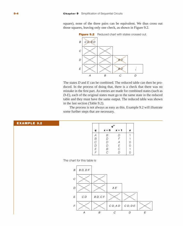
The states D and E can be combined. The reduced table can then be pro-duced. In the process of doing that, there is a check that there was nomistake in the first part. As entries are made for combined states (such asD-E), each of the original states must go to the same state in the reducedtable and they must have the same output. The reduced table was shownin the last section (Table 9.2).
The process is not always as easy as this. Example 9.2 will illustratesome further steps that are necessary.
square), none of the three pairs can be equivalent. We thus cross outthose squares, leaving only one check, as shown in Figure 9.2.
9-4 Chapter 9 Simplification of Sequential Circuits
Figure 9.2 Reduced chart with states crossed out.
B C E, B D
B D
B D
C
D
E
A B C D
�
EXAMPLE 9.2q�
q x � 0 x � 1 z
A B D 1B D F 1C D A 0D D E 0E B C 1F C D 0
The chart for this table is
B D, D F
B D, C F
C D, A D C D, D E
B
C
D
C D
A E
E
F
A B C D E
mar91647_c09_000_000.qxd 11/24/08 12:08 PM Page 9-4

Note that the first entry could have been written BDF, that is, all three statesmust be equivalent. (Indeed, since this is the condition for A and B to beequivalent, we then require that A, B, D, and F all be equivalent.) Goingthrough the table, we see that B and D cannot be equivalent; neither can Aand D, nor D and E. That reduces the table to the following:
What remains is that A is equivalent to E if C is equivalent to D and that C isequivalent to D if A is equivalent to E. That allows us to check off both ofthese, producing the reduced table:
B D, D F
B D, C F
C D, A D C D, D E
B
C
D
C D
A E
E
F
A B C D E
9.1 A Tabular Method for State Reduction 9-5
EXAMPLE 9.3
q�
q x � 0 x � 1 z
A-E B C-D 1B C-D F 1
C-D C-D A-E 0F C-D C-D 0
Before looking at some more complex examples, we want to empha-size the effect that the output column has on the process. The state tableand chart of Example 9.3 correspond to a system with the same next statebehavior as that of Example 9.2, but a different output column.
The chart is different, because the pairings that are automatically X’d (dueto the output) are different.
q�
q x � 0 x � 1 z
A B D 1B D F 1C D A 1D D E 0E B C 0F C D 0
mar91647_c09_000_000.qxd 11/24/08 12:08 PM Page 9-5

None of the conditions can be satisfied, and thus, no states can be com-bined and the state table cannot be reduced.
Sometimes, when the obvious unequivalences are crossed off, theremay be some doubt as to whether the remaining states can be combined.We could try to combine them all and develop the reduced state table. Ifwe were mistaken, it will quickly become evident. Also, if we find one ormore equivalences before completing the process, we can reduce the tableand start the process over. That is somewhat more work, but the chart forthe reduced table is much smaller and may be easier to work with.
B D F
B D, C E
B C DC D E
A B D A F
B
C
D
E
F
A B C D E
9-6 Chapter 9 Simplification of Sequential Circuits
EXAMPLE 9.4q� z
q x � 0 x � 1 x � 0 x � 1
A F B 0 0B E G 0 0C C G 0 0D A C 1 1E E D 0 0F A B 0 0G F C 1 1
The chart for this table is
E F, B G
B G, C F
E F, B D
A E, B DA C, B GA E, B G
C E
D G D G
B
C
D
E
F
G A F
A B C D E F
mar91647_c09_000_000.qxd 11/24/08 12:08 PM Page 9-6

Note that we checked AF, since the requirement that A is equivalent to F isjust that F is equivalent to A. That is always true. We first go through thechart to find which conditions cannot be met, crossing them out. We alsonote that condition AF has already been checked and therefore D and G areequivalent. During this pass, we may take advantage of the new equiva-lences and the cross outs or we may wait until the next pass. Waiting untilthe next pass, the table becomes
We now have A equivalent to F and D equivalent to G. The latter satisfies thecondition for C being equivalent to E and B being equivalent to E. Finally,since C and E are equivalent, B is equivalent to C. That makes B, C, and Eall equivalent. Thus, the reduced table has three states—A (A-F ), B (B-C-E ),and D (D-G).
E F, B G
B G, C F
E F, B D
A E, B DA C, B GA E, B G
C E
D G D G
B
C
D
E
F
G A F
A B C D E F
�
�
9.1 A Tabular Method for State Reduction 9-7
q� zq x � 0 x � 1 x � 0 x � 1
A A B 0 0B B D 0 0D A B 1 1
q� zq x � 0 x � 1 x � 0 x � 1
A A B 0 0B E D 0 0C C D 0 0D A C 1 1E E D 0 0
With the last chart above, we could have reduced the system to one withfive states, just using the equivalences checked (A-F and D-G). That wouldproduce the new table
mar91647_c09_000_000.qxd 11/24/08 12:08 PM Page 9-7
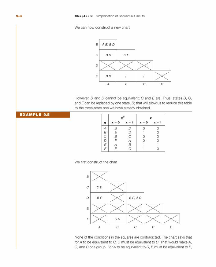
We can now construct a new chart
However, B and D cannot be equivalent; C and E are. Thus, states B, C,and E can be replaced by one state, B; that will allow us to reduce this tableto the three-state one we have already obtained.
A E, B D
B D
B D C E
B
C
D
E
A B C D
� �
9-8 Chapter 9 Simplification of Sequential Circuits
EXAMPLE 9.5q� z
q x � 0 x � 1 x � 0 x � 1
A B D 0 0B E D 1 0C B C 0 0D F A 0 0E A B 1 1F E C 1 0
We first construct the chart
None of the conditions in the squares are contradicted. The chart says thatfor A to be equivalent to C, C must be equivalent to D. That would make A,C, and D one group. For A to be equivalent to D, B must be equivalent to F,
C D
B
C
D B F B F, A C
E
C DF
BA C D E
mar91647_c09_000_000.qxd 11/24/08 12:08 PM Page 9-8

and for B to be equivalent to F, C must be equivalent to D. Finally, C is equiv-alent to D if B is equivalent to F and A is equivalent to C. All of these canbe true, producing a reduced state table with only three states, A (A-C-D),B (B-F), and E. (As we construct that table, we can check our conclusionsfrom the chart by making sure that all states in one group go to a state in asingle group for each input.)
9.1 A Tabular Method for State Reduction 9-9
EXAMPLE 9.6
q� zq x � 0 x � 1 x � 0 x � 1
A B A 0 0B E A 1 0E A B 1 1
As our last example of this technique, we will consider a system with twoinputs, x y. Thus, there are four columns in the next state section of thetable.
The charting problem is really no different than before; we just have moreconditions, since equivalent states must go to equivalent states for all fourinput combinations (that is, all four columns). The chart then becomes
None of the groups of three states shown in the chart can be equivalent;one of each has a different output than the other two. Crossing out thosesquares, we have
B EC D F
A E
B
C
DA B FC D
B C DC FB D
E A B C
F B D
BA C D E
x y q�
q 0 0 0 1 1 0 1 1 z
A B A F D 1B E A D C 1C A F D C 0D A A B C 1E B A C B 1F A F B C 0
mar91647_c09_000_000.qxd 11/24/08 12:08 PM Page 9-9

That leaves three pairings intact, A E, B D, and C F. The only requirementfor any of these is that one of the others be equivalent. Thus, we can reducethis to three states as follows:
B EC D F
C FB D
B D
A E
B
C
D
E
F
A B C D E
A B FC D
B C D A B C
9-10 Chapter 9 Simplification of Sequential Circuits
[SP 1; EX 1]
x y q�
q 0 0 0 1 1 0 1 1 z
A B A C B 1B A A B C 1C A C B C 0
9.2 PARTITIONS
A partition on the states of a system is a grouping of the states of thatsystem into one or more blocks. Each state must be in one and only oneblock. For a system with four states, A, B, C, and D, the complete list ofpartitions is
P0 � (A)(B)(C)(D) P8 � (AC)(BD)
P1 � (AB)(C)(D) P9 � (AD)(BC)
P2 � (AC)(B)(D) P10 � (ABC)(D)
P3 � (AD)(B)(C) P11 � (ABD)(C)
P4 � (A)(BC)(D) P12 � (ACD)(B)
P5 � (A)(BD)(C) P13 � (A)(BCD)
P6 � (A)(B)(CD) PN � (ABCD)
P7 � (AB)(CD)
This list of partitions does not depend on the details of the state table,only on the list of states. P0 is the partition with each state in a separateblock; PN is the partition with all of the states in the same block. We willbe concerned with partitions that have special properties for a particularstate table. There are three categories of partitions that will be of interest.To illustrate these, we will use Table 9.3.
mar91647_c09_000_000.qxd 11/24/08 12:08 PM Page 9-10

Any partition with two blocks can be used to assign one of the statevariables. Those states in the first block would be assigned 0 and those inthe second block 1 (or vice versa). P7 through P13 meet that requirement.(We write partitions in alphabetic order; thus, state A will usually beassigned all 0’s.) In a four-state system, there are only three pairs of par-titions that can be used for a two-variable state assignment, P7 and P8, P7
and P9, and P8 and P9. The three are shown in Table 9.4.
9.2 Partitions 9-11
Table 9.5 An unsuccessfulassignment.
q q1 q2
A 0 0B 1 0C 0 1D 1 0
P8 P11
If we try any other pair of two-block partitions, we do not have an ade-quate state assignment. For example, using P8 and P11, we get the assign-ment of Table 9.5. Note that states B and D have the same assignment.
A second useful class of partitions are those for which all of thestates in each block have the same output for each of the inputs. Suchpartitions are referred to as output consistent. P0 is always output consis-tent; for Table 9.3, the other output consistent partitions are
P2 � (AC)(B)(D)
P5 � (A)(BD)(C)
P8 � (AC)(BD)
Knowing the block of an output consistent partition and the input isenough information to determine the output (without having to knowwhich state within a block).
For some partitions, knowing the block of the partition and the inputis enough information to determine the block of the next state. Such apartition is said to have the substitution property and is referred to as anSP partition. PN is always SP since all states are in the same block, andP0 is always SP since knowing the block is the same as knowing the state.Others may be SP, depending on the details of the state table. For thisstate table, there are two nontrivial SP partitions (those other than P0 andPN), namely,
P7 � (AB)(CD)
P9 � (AD)(BC)
If a partition other than P0 is both SP and output consistent, then wecan reduce the system to one having just one state for each block of thatpartition. (That should be obvious since knowing the input and the block
Table 9.3 State table to illustratetypes of partitions.
q�
q x � 0 x � 1 z
A C A 1B D B 0C A B 1D B A 0
q q1 q2
A 0 0B 0 1C 1 0D 1 1
P7 P8
(a)
q q1 q2
A 0 0B 0 1C 1 1D 1 0
P7 P9
(b)
q q1 q2
A 0 0B 1 1C 0 1D 1 0
P8 P9
(c)
Table 9.4 State assignments for four states.
mar91647_c09_000_000.qxd 11/24/08 12:08 PM Page 9-11

of the partition is all we need to know to determine the output, since itis output consistent, and to determine the next state, since it is SP). Forthis example, neither of the SP partitions is also output consistent. InExample 9.1, the partition
(A)(B)(CD)
is both SP and output consistent; thus, we were able to reduce the systemto one with only three states.
Before developing a method for finding all SP partitions, we willlook at Example 9.7. It will help us understand the application of the var-ious categories of partitions.
9-12 Chapter 9 Simplification of Sequential Circuits
EXAMPLE 9.7
For this state assignment, we obtain the output equation and the inputs toD flip flops
z � q2 � q3
D1 � xq1 � xq3
D2 � x�q�1q�2 � xq�1q�3
D3 � x�q2q3 � x�q1 � xq�1q�3
This requires 11 gates and 25-gate inputs (for either AND and OR or NAND,including a NOT for x�). We would need four 7400 series integrated circuitpackages to implement the combinational logic with NAND gates. (Thedevelopment of the equations and the gate count is left as an exercise.)
If we make the state assignment using the following three partitions:
P1 � (ABC)(DE ) SP
P2 � (AB)(CDE ) SP
P3 � (AE )(BCD) output consistent
we have
q�
q x � 0 x � 1 z
A C D 0B C E 1C A D 1D B E 1E B E 0
Assignment 1q q1 q2 q3
A 0 0 0B 0 0 1C 0 1 0D 0 1 1E 1 0 0
Assignment 2q q1 q2 q3
A 0 0 0B 0 0 1C 0 1 1D 1 1 1E 1 1 0
Logic Equations
z � q3D1 � xD2 � x � q2�D3 � x�q1 � x�q�2 � {q�2q�3 or q�1q�3} � xq�1q2
mar91647_c09_000_000.qxd 11/24/08 12:08 PM Page 9-12

9.2 Partitions 9-13
This requires only seven gates, 16 inputs, and three 7400 series NAND gateintegrated circuit packages. D3 is the only complex function.
We saw the advantage of using an output consistent partition, thatthe output is just equal to that variable or its complement. Thus, z is onlya function of q3.
We saw the advantage of using an SP partition to assign a state vari-able, that the next state of that variable is only a function of the input, x,and that variable (no matter how many flip flops are needed to implementthat system). Since q1 and q2 are assigned using SP partitions, D1 is onlya function of x (could also depend on q1), and D2 is only a function of xand q2. For JK flip flops, the inputs are functions only of x (x, x�, and 1are the only possibilities). Indeed, we do not need to deal with the wholestate table for the implementation of flip flops assigned according to SPpartitions; we only need a block table. Thus, for the flip flops assignedaccording to partition P1 � (ABC)(DE), where the first block is assigned0, we would have Table 9.6, which gives
D1 � q1� � x J1 � x K1 � x�
This is, of course, the same answer we got for D1 before. We could fol-low this approach for D2 or J2 and K2 as well, but would need the fullfour-variable truth table to solve for the inputs to q3.
9.2.1 Properties of Partitions
First, we will define, for pairs of partitions, the relationship greater thanor equal (�) and two operators, the product and the sum.
■ Pa � Pb if and only if all states in the same block of Pb are also inthe same block of Pa.
For example,
P10 � (ABC)(D) � P2 � (AC)(B)(D)
since the only states in the same block of P2 (A and C) are also in thesame block of P10. P0 is the smallest partition; all other partitions aregreater than it. PN is the largest partition; it is greater than all others. Notall partitions are ordered. For example, P1 is neither � nor � P2.
■ The product of two partitions is written Pc � PaPb.
Two states are in the same block of the product Pc if and only ifthey are in the same block of both Pa and Pb.
For example,
P12P13 � {(ACD)(B)}{(A)(BCD)} � (A)(B)(CD) � P6
Table 9.6 Truth table for q1.
x q1 q1� J K
(ABC) 0 0 0 0 X(DE ) 0 1 0 X 1(ABC) 1 0 1 1 X(DE ) 1 1 1 X 0
mar91647_c09_000_000.qxd 11/24/08 12:08 PM Page 9-13

The only states that are in the same block of both P12 and P13 are C andD; they are then together in the product. The partitions Pa and Pb arealways greater than or equal to the product Pc. If the two partitions areordered, the product is equal to the smaller one. For example, P6 � P13
and thus, P6P13 � P6. It is also clear from the definitions that, for anypartition, Pa
PaP0 � P0 and PaPN � Pa
■ The sum of two partitions is written Pc � Pa � Pb.
Two states are in the same block of the sum Pd if they are in thesame block of either Pa or Pb or both.
For example,
P2 � P5 � {(AC)(B)(D)} � {(A)(BD)(C)} � P8 � (AC)(BD)
The sum sometimes brings together states that are not in the same blockof either since whole blocks are combined. Consider the followingexample:
Pa � (AB)(C)(DF)(EG)
Pb � (ACD)(BG)(E)(F)
Pa � Pb � (ABCDEFG) � PN
Since A and B are in the same block of Pa and A, C, and D are in the sameblock of Pb, then ABCD are in one block of the sum. But F is in the sameblock as D in Pa and G is in the same block as B of Pb; so they must beincluded with ABCD. Finally, E is in the same block as G in Pa, produc-ing a sum of PN. The sum Pc is always greater than or equal to bothPa and Pb. If Pa and Pb are ordered, the sum equals the greater. Thus,P6 � P13 � P13. Also,
Pa � P0 � Pa and Pa � PN � PN
9.2.2 Finding SP Partitions
The process of finding all SP partitions has two steps.
We must ask what is required to make a partition SP if these twostates are in the same block, that is, what makes these two states equiva-lent. They must go to equivalent states for each input. We must thenfollow through, determining what groupings are forced.
Step 1: For each pair of states, find the smallest SP partition thatputs those two states in the same block.
9-14 Chapter 9 Simplification of Sequential Circuits
mar91647_c09_000_000.qxd 11/24/08 12:08 PM Page 9-14

We will use the state table of Table 9.3, repeated here without theoutput columns (since that has no relevance to finding SP partitions) asTable 9.7.
For A to be equivalent to B, C must be equivalent to D. We continueby checking what conditions are required to make C equivalent to D. Inthis example, the only requirement is that A be equivalent to B. Thus, wehave our first SP partition
(AB) → (CD) → → (AB)(CD) � P1
where the right arrow (→) is used to indicate requires, and the doublearrow indicates the smallest SP partition that results. Sometimes, we findno new conditions and other times the conditions force all of the statesinto one block, producing PN.
The next step is
(AC) → (AB) → (CD) → (ABCD) � PN
(Since C must be with A and B must be with A, then A, B, and C must allbe together. But then D must be with C, resulting in PN.) The balance ofstep 1 produces
(AD) → (BC) → → (AD)(BC) � P2
(BC) → (AD) → → (AD)(BC) � P2
(BD) → (AB) → → PN
(CD) → (AB) → → (AB)(CD) � P1
In this process, we do not need to find the sum of another partitionwith any two-block partition since that always results in either the two-block partition or PN. Also, if one partition is greater than another, itssum is always the greater partition. We can omit those additions, too.
For the first example, there are no sums to compute, since the onlytwo unique nontrivial (that is, other than P0 and PN) SP partitions formedby step 1 are both two-block.
Step 2: Find the sum of all of the SP partitions found in step 1 and,if new ones are found, repeat step 2 on these new ones.
9.2 Partitions 9-15
EXAMPLE 9.8
Table 9.7 A state table forfinding SPpartitions.
q�
q x � 0 x � 1
A C AB D BC A BD B A
q�
q x � 0 x � 1 z
A C D 1B C D 0C B D 1D C A 1
Step 1 produces five SP partitions.
mar91647_c09_000_000.qxd 11/24/08 12:08 PM Page 9-15

(AB) → √* → → P1 � (AB)(C)(D)
(AC) → (BC), (BC) → ok → → P2 � (ABC)(D)
(AD) → √ → → P3 � (AD)(B)(C)
(BC) → √ → → P4 � (A)(BC)(D)
(BD) → (AD) → (ABD) → → P5 � (ABD)(C)
(CD) → (BC), (AD) → → PN
Step 2 really only requires three sums, although we will show all 10below:
P1 � P2 � (ABC)(D) → → P2 not needed
P1 � P3 � (ABD)(C) → → P5
P1 � P4 � (ABC)(D) → → P2
P1 � P5 � (ABD)(C) → → P5 not needed
P2 � P3 → → PN not needed
P2 � P4 � (ABC)(D) → → P2 not needed
P2 � P5 → → PN not needed
P3 � P4 � (AD)(BC) → → P6 � (AD)(BC)
P3 � P5 � (ABD)(C) → → P5 not needed
P4 � P5 → → PN not needed
Those partitions shown in bold are two-block and thus never produceanything new. Only one new SP partition is found by step 2.
9-16 Chapter 9 Simplification of Sequential Circuits
*Here is the first example of a pairing that requires no other states to be combined. Itresults in a partition where these two states are in one block and all others are bythemselves.
EXAMPLE 9.9q�
q x � 0 x � 1 z
A C D 0B D A 0C E D 0D B A 1E C D 1
Step 1 of the process produces five SP partitions, as follows:
(AB) → (CD)(AD) → (ACD) → (BCE) → → PN
(AC) → (CE ) → → (ACE)(B)(D) � P1
(AD) → (BC) → (DE) → → (ADE)(BC) � P2
(AE ) → √ → → (AE)(B)(C)(D) � P3
(BC) → (ADE) → → P2
(BD) → √ → → (A)(BD)(C)(E ) � P4
(BE) → (ACD) → (BCE ) → → PN
(CD) → (BE)(AD) → (BC) → → PN
(CE) → √ → → (A)(B)(CE )(D) � P5
(DE ) → (BC)(AD) → (ADE) → → P2
mar91647_c09_000_000.qxd 11/24/08 12:08 PM Page 9-16

Table 9.9 Reduced statetable.
q�
q x � 0 x � 1 z
A C A 1B C A 0C B A 1
For step 2, we add each of the pairs of partitions found in step 1,except that we do not need to add P2 to anything (since it is two-block) andP1 need not be added to P3 or P5 (since it is greater than each of them).
P1 � P4 � (ACE )(BD) � P6
P3 � P4 � (AE )(BD)(C) � P7
P3 � P5 � (ACE)(B)(D) � P1
P4 � P5 � (A)(BD)(CE ) � P8
We now add pairs of these new partitions (with the same exceptions asabove); there is only one sum (which does not produce anything new):
P7 � P8 � (ACE )(BD) � P6
If there were new partitions of more than two blocks, they must also beadded.
For this example, there are eight nontrivial SP partitions, of which twoare two-block and none are output-consistent. We will return to this statetable in the next sections when we discuss state reduction and how tomake good state assignments.
9.3 STATE REDUCTION USING PARTITIONS
Any partition that is both output consistent and SP can be used to reducethe system to one with one state for each block of that partition. Just asthere is always a unique largest SP partition (PN), there is always a uniquelargest output consistent SP partition. That is the one with the fewestblocks and thus corresponds to the reduced system with the fewest num-ber of states.*
For the state table of Example 9.8, repeated here as Table 9.8, the onlySP partition that is output consistent is P3 � (AD)(B)(C); thus, this statetable can be reduced to one with three states (one for each block of P3).
We will call the combined state A (rather than A-D); the reducedtable is shown in Table 9.9.
We do not need to recalculate all of the SP partitions (although forthis small example, that would be very easy). Any SP partition of theoriginal system that is greater than (�) the one used to reduce the systemis still SP. For this example, only P5 � P3. Thus, we get one nontrivial SPpartition for the reduced system, namely,
P5� � (AB)(C)
where AD of the original P5 has been replaced by the new state A. The last state table of the previous section, Example 9.9, did not
have any output consistent SP partitions. Thus, it can not be reduced.
9.3 State Reduction Using Partitions 9-17
[SP 2, EX 2]
*It is possible that PN is output consistent; but that is a combinational system, where theoutput does not depend on the state.
Table 9.8 A reducible statetable.
q�
q x � 0 x � 1 z
A C D 1B C D 0C B D 1D C A 1
mar91647_c09_000_000.qxd 11/24/08 12:08 PM Page 9-17

We will now look at two state tables with the same next state section, butdifferent output columns.
9-18 Chapter 9 Simplification of Sequential Circuits
EXAMPLE 9.10q�
q x � 0 x � 1 z
A C D 0B D A 1C E D 0D B A 0E C D 0
q�
q x � 0 x � 1 z
A C D 0B D A 1C E D 0D B A 1E C D 0
q�
q x � 0 x � 1 z
A-C-E A-C-E D 0B D A-C-E 1D B A-C-E 0
The set of SP partitions for these two is the same as those for Example 9.9,since the substitution property does not depend on the output. Repeatingthe complete list here, we have
P1 � (ACE )(B)(D)
P2 � (ADE )(BC)
P3 � (AE )(B)(C)(D)
P4 � (A)(BD)(C)(E )
P5 � (A)(B)(CE )(D)
P6 � (ACE )(BD)
P7 � (AE )(BD)(C)
P8 � (A)(BD)(CE )
In the first table, P1, P3, and P5 are the only output consistent partitions.Since
P1 � (ACE )(B)(D)
is greater than either of the others, we will use it to reduce the system to onewith three states, as follows:
(We labeled the combined state with a compound name; we could have justcalled it A.) Note that only P6 � P1; thus, the only SP partition of the reducedsystem is
P6� � (A-C-E )(BD)
For the second state table, P1, P3, P4, P5, P6, and P8 are all outputconsistent. The largest is
P6 � (ACE )(BD)
as can be seen from the chart below, where the smaller ones are on the left.
mar91647_c09_000_000.qxd 11/24/08 12:08 PM Page 9-18

We can thus reduce the system to one with only two states, A (ACE ) andB (BD), as shown below. This system requires only one flip flop.
(A E ) (B) (C) (D)
(A C E ) (B) (D)
(A C E ) (B D)(A) (B) (C E ) (D)
(A) (B D) (C E )
(A) (B D) (C) (E )
�
�
�
�
�
�
9.3 State Reduction Using Partitions 9-19
EXAMPLE 9.11
q�
q x � 0 x � 1 z
A A B 0B B A 1
The computation of all of the SP partitions for a fairly large systemcan be quite time-consuming. If our interest is in reducing the system toone with the minimum number of states, we can do that immediately whenwe find an output consistent SP partition. Consider the following example.
As we begin the process of finding SP partitions, we get
(AB) → (BD)(AE ) → (DF )(AG)(CE ) → → PN
(AC) → (BG)(AE ) → (ACE ) → → (ACE )(BG)(D)(F )
This SP partition is also output consistent. Therefore, we could stop andreduce the system to one with four states (one for each block) and find theSP partitions of that smaller system.
q�
q x � 0 x � 1 z
A B E 0B D A 1C G A 0D F G 1E B C 0F D G 1G D E 1
q�
q x � 0 x � 1 z
A B A 0B D A 1D F B 1F D B 1
mar91647_c09_000_000.qxd 11/24/08 12:08 PM Page 9-19

We can now find the SP partitions of this smaller system
(AB) → (BD) → (DF ) → → PN
(AD) → (AB)*(BF) → → PN
(AF ) → (BD)(AB) → → PN
(BD) → (DF )(AB) → → PN
(BF ) → (AB) → → PN
(DF ) → √ → (A)(B)(DF)
This system can be reduced further, to one with three states, since the SPpartition is also output consistent. The smallest equivalent system is thus
9-20 Chapter 9 Simplification of Sequential Circuits
EXAMPLE 9.12
*Since we found that the only SP partition that combines A and B is PN, we can stoplooking; this must also produce PN.
q�
q x � 0 x � 1 z
A B A 0B D A 1D D B 1
As a final example, consider the following state table, where five dif-ferent output columns are shown. (This is a Moore system with an outputthat does not depend on the input; we will consider the different outputsas five different problems.)
We will start by finding all of the SP partitions. That, of course, does notdepend upon which output column is used.
(AB) → (BC)(DE ) → (AE ) → → PN
(AC) → (AD) → (AE ) (BC) → → PN
(AD) → (DE)(BC) → → (ADE )(BC) � P1
(AE ) → √ → → (AE )(B)(C)(D) � P2
(BC) → (AE ) → → (AE )(BC)(D) � P3
(BD) → √ → → (A)(BD)(C)(E ) � P4
(BE ) → (BC)(DE ) → (AE ) → → PN
(CD) → (AE )(BC) → → (AE)(BCD) � P5
(CE ) → (AD) → (DE )(BC) → → PN
(DE ) → (BC) → (AE ) → → P1
q�
q x � 0 x � 1 z1 z2 z3 z4 z5
A D B 0 0 0 1 1B E C 0 0 1 0 1C A B 1 1 0 0 1D E C 1 1 1 1 1E D B 1 0 0 1 1
mar91647_c09_000_000.qxd 11/24/08 12:08 PM Page 9-20

9.3 State Reduction Using Partitions 9-21
Now, forming sums, we obtain only one new partition
P2 � P4 � (AE)(BD)(C) � P6
Thus, there are six nontrivial SP partitions.For the first output column, none of the SP partitions are output con-
sistent. Thus, the state table cannot be reduced. (We will return to thisexample in the next section and determine a good state assignment.)
For the second output column, only P2 is output consistent. Thus, thissystem can be reduced to one with four states (replacing A and E by a statecalled A).
q�
q x � 0 x � 1 z3
A B B 0B A C 0C A B 1
q�
q x � 0 x � 1 z2
A D B 0B A C 0C A B 1D A C 1
Since any SP partition that is greater than P2 is an SP partition of thereduced table (with states A and E shown as one, just A), we can see thatthe SP partitions are
P1� � (AD)(BC)
P3� � (A)(BC)(D)
P5� � (A)(BCD)
P6� � (A)(BD)(C)
For the third output column, P2, P4, and P6 are all output consistent.Since P6 is the largest of these, it is used to reduce the system to one withonly three states.
The only nontrivial SP partition for this system is
P5� � (A)(BC)
For the fourth output column, P1 is output consistent, reducing thestate table to one with only two states.
mar91647_c09_000_000.qxd 11/24/08 12:08 PM Page 9-21

Finally, for the last output column, there was no need to find the SPpartitions; PN is output consistent; the system is combinational. It does notdepend on the state.
z � 1
9.4 CHOOSING A STATE ASSIGNMENT
In this section, we will look at a strategy for making a “good” stateassignment. We will first find all of the SP partitions, then reduce the sys-tem if possible, and finally make a state assignment to solve the problem.We have three levels of work, depending upon how important it is toreduce the cost of the combinational logic. If an absolute minimum isrequired, we must try all possible sets of two-block partitions for whichthe product is P0. For three or four states, there are only three suchassignments, and it is fairly easy to do that. For five states, however, thatnumber goes up to 140, and this method is not practical. (It rises to 420for six states, to 840 for seven or eight states, and to over 10 million fornine states.) If we can use two-block SP partitions for one or more of thevariables, that is almost always preferable (as long as we do not increasethe number of variables). We can then try to group states that are in thesame block of multiblock SP partitions or to use partitions that corre-spond to one or more of the output columns for the other variables. Thiswill usually lead to a pretty good solution. Last, and least likely to pro-duce good results, we could choose an assignment at random, say using000 for A, 001 for B, and so forth. Sometimes, that will lead to a goodsolution. But more often, it will result in a more costly system.
To illustrate this, we will consider the example in Table 9.10. TheSP partitions are
P1 � (AB)(CD)
P2 � (AD)(B)(C)
P3 � (A)(BC)(D)
P2 � P3 � P4 � (AD)(BC )
There are no output consistent SP partitions. There are two SP partitionsthat could be used for state assignment, namely, P1 and P4. That wouldproduce the assignment of Table 9.11 and the D flip flop input equationsshown.
9-22 Chapter 9 Simplification of Sequential Circuits
Table 9.10 State assignmentexample.
q�
q x � 0 x � 1 z
A B C 0B A D 1C A D 0D B C 1
q�
q x � 0 x � 1 z4
A A B 0B A B 1
[SP 3, EX 3]
mar91647_c09_000_000.qxd 11/24/08 12:08 PM Page 9-22

9.4 Choosing a State Assignment 9-23
Since both flip flops were assigned according to an SP partition, theinput equations are very simple.
If we repeat the design, using the output consistent partition forq2, we get the state assignment of Table 9.12 and the equations shownbeside it.
Table 9.11 State assignment.
q q1 q2
A 0 0B 0 1C 1 1D 1 0
z � q�1q2 � q1q�2D1 � xD2 � q�2
Notice that D1 is unchanged. Since it was assigned according to the sameSP partition as before, its behavior does not depend on the rest of theassignment. Also, z becomes simple, since q2 is assigned according toan output consistent partition. This is an extreme case; D2 is particu-larly complex. If, on the other hand, we assigned q1 according to theoutput consistent partition and q2 according to P4 (as in the first exam-ple), we would get the assignment of Table 9.13 and the equations shownbelow.
Table 9.13 State assignment.
q q1 q2
A 0 0B 1 1C 0 1D 1 0
z � q1
D1 � x�q�2 � xq2
D2 � q�2
Table 9.12 State assignment.
q q1 q2
A 0 0B 0 1C 1 0D 1 1
z � q�2D1 � xD2 � x�q�1q�2 � x�q1q2 � xq�1q2 � xq1q�2
Now, D1 is more complex, although the total cost of combinational logicis the same as for the first assignment. Costs do not vary as much in twoflip flop circuits as they do in larger ones.
We will illustrate the procedure with two of the output columns fromExample 9.12.
mar91647_c09_000_000.qxd 11/24/08 12:08 PM Page 9-23

We will first consider the table of Example 9.12 with output column z2.
9-24 Chapter 9 Simplification of Sequential Circuits
EXAMPLE 9.13
q�
q x � 0 x � 1 z2
A D B 0B E C 0C A B 1D E C 1E D B 0
q�
q x � 0 x � 1 z2
A D B 0B A C 0C A B 1D A C 1
The first step is to see if the system can be reduced. The SP partition,(AE )(B)(C)(D) is output consistent, and thus this system can be reduced toone with four states, as shown below.
The SP partitions for this are (as we found earlier)
P1� � (AD)(BC) P5
� � (A)(BCD)
P3� � (A)(BC)(D) P6
� � (A)(BD)(C)
The best assignment seems to be the one that uses P1� and the output
consistent partition (POC � (AB)(CD)). That produces
z � q2
D1 � x
D2 � q�1q�2 � xq2
If, instead, we used output column z1, there could be no reduction, andthree flip flops would be needed. However, there are 2 two-block SP parti-tions, in addition to the output consistent one, that can be used for the stateassignment.
P1 � (ADE )(BC)
P5 � (AE )(BCD)
POC � (AB)(CDE )
This produces the state assignment
q q1 q2 q3
A 0 0 0B 1 1 0C 1 1 1D 0 1 1E 0 0 1
and the equations
mar91647_c09_000_000.qxd 11/24/08 12:08 PM Page 9-24

z � q3
D1 � x
D2 � x � q�2
D3 � {x�q�1 or x�q�2} � q�1q2 � {q2q�3 or q1q�3}
This requires only five gates plus the NOT gate for x�.
9.4 Choosing a State Assignment 9-25
EXAMPLE 9.14
The nontrivial SP partitions are
P1 � (AB)(C)(DF )(E ) P6 � (AB)(CE )(DF )
P2 � (ABC)(DEF ) P7 � (ABDF )(C)(E )
P3 � (AD)(B)(C)(E )(F ) P8 � (ABDF )(CE )
P4 � (AF)(BD)(C)(E ) P9 � (AD)(BF )(C)(E )
P5 � (A)(BF )(C)(D)(E )
As can be seen, none of these are output consistent; thus the table cannotbe reduced.
For the first two variables, we will use the 2 two-block SP partitions, P2
and P8. The product of these are
P1 � (AB)(C)(DF )(E )
For the third variable, we need a partition that separates A from B and Dfrom F. There are many that will do that; we chose
P9 � (AF )(BCDE )
because that corresponds to the second output column and will simplifysomewhat the expression for z.
First, we will construct next block tables for q1 and q2.
q� zq x � 0 x � 1 x � 0 x � 1
A D C 0 1B F C 0 0C E A 0 0D A C 1 0E C B 1 0F B C 1 1
q1�
q1 x � 0 x � 1
0 1 01 0 0
q2�
q2 x � 0 x � 1
0 0 11 1 0
This produces
D1 � x�q�1 D2 � xq�2 � x�q2
For q3 and z, we will need the state assignment and truth table:
mar91647_c09_000_000.qxd 11/24/08 12:08 PM Page 9-25

9-26 Chapter 9 Simplification of Sequential Circuits
(We do not need columns for q1� and q2
�, since we already computed theinputs for those flip flops from the next block table.) The resulting maps are
From this, we can find
D3 � x�q�2q�3 � xq�1q2 z � x�q1 � xq3
The advantage of using SP partitions is even more dramatic with JKflip flops (since J and K do not depend on the state of that flip flop). Thus,for this example,
J1 = x� K1 = 1J2 = x K2 = xJ3 = x�q2� + xq1�q2 K3 = 1
If, instead, we used the state assignment
00 01 11 10
00
01
11
10
x q1
q2 q3
X X X
1
X
1 1
00 01 11 10
00
01
11
10
x q1
z
q2 q3
X X X
1
X
1
1 1 1
q3★
q q1 q2 q3
A 0 0 1B 0 0 0C 0 1 0D 1 0 0E 1 1 0F 1 0 1
P2 P8 P9
x q1 q2 q3 q3� z
B 0 0 0 0 1 0A 0 0 0 1 0 0C 0 0 1 0 0 0— 0 0 1 1 X XD 0 1 0 0 1 1F 0 1 0 1 0 1E 0 1 1 0 0 1— 0 1 1 1 X XB 1 0 0 0 0 0A 1 0 0 1 0 1C 1 0 1 0 1 0— 1 0 1 1 X XD 1 1 0 0 0 0F 1 1 0 1 0 1E 1 1 1 0 0 0— 1 1 1 1 X X
q q1 q2 q3
A 0 0 0B 0 0 1C 0 1 0D 0 1 1E 1 0 0F 1 0 1
mar91647_c09_000_000.qxd 11/24/08 12:08 PM Page 9-26

we would obtain the equations
z � x�q1 � q1q3 � xq�1q�2q�3 � x�q2q3
D1 � x�q�1q�2q3 � x�q2q�3
D2 � xq3 � x�q�2q�3 � q�1q�2q�3
D3 � x�q�1q�2 + xq1q�3 � x�q1q3
These equations are much more complex than the previous solution.
9.4 Choosing a State Assignment 9-27
EXAMPLE 9.15
The SP partitions are
P1 � (ABD)(C)(E ) P4 � (A)(B)(CE )(D)
P2 � (ABDE )(C) P5 � (A)(B)(C)(DE )
P3 � (A)(B)(CDE ) P6 � (ABD)(CE )
None of these is output consistent; therefore, the system cannot bereduced. Although there are 2 two-block partitions, we cannot use both ofthem, since their product is P1, which has three states in the same block.One more two-block partition cannot separate these three states. We canuse P6 and the output consistent partition,
P7 � (ACD)(BE )
for two of the variables. Their product is
(AD)(B)(C)(E )
We now need to choose one more partition to separate A and D. From thelist of SP partitions, P3 is attractive. It groups C, D, and E. We could useeither
P8 � (AB)(CDE ) or P9 � (A)(BCDE )
The two state assignments are
q�
q x � 0 x � 1 z
A B C 0B D C 1C A E 0D A C 0E A C 1
q q1 q2 q3
A 0 0 0B 0 1 0C 1 0 1D 0 0 1E 1 1 1
q q1 q2 q3
A 0 0 0B 0 1 1C 1 0 1D 0 0 1E 1 1 1
mar91647_c09_000_000.qxd 11/24/08 12:08 PM Page 9-27

The resulting sets of equations for the first assignment are
J1 � x K1 � x�
J2 � x�q�3 � xq1 K2 � 1
J3 � x � q2 K3 � x�
z � q2
For the second assignment, J1, K1, J2, K2, and z are unchanged; the othersbecome
J3 � 1 K3 � x�q�2 � x�q1
If, instead, we use the first five combinations for the five states, the equa-tions become
J1 � q2q�3 K1 � 1
J2 � x � q3 K2 � x� � q�3
J3 � x�q�1q�2 K3 � x � q2
z � q1 � q�2q3
The cost of this combinational logic is about double that of the first solution.
The choice of state assignment is more of an art than a science.Surely, we want to use two-block SP partitions when possible. But whenwe run out of those, we use the output consistent partition and the group-ings suggested by other SP partitions (if there are any).
This approach does not guarantee a minimum solution. The onlyway to do that is to try all possible sets of partitions. (In some unusualcircumstances, it may even be possible to find a less costly solutionwith an extra flip flop or without reducing the number of states to aminimum.)
9.5 SOLVED PROBLEMS
1. Reduce each of the following systems to ones with theminimum number of states using the tabular method.
a. b.
9-28 Chapter 9 Simplification of Sequential Circuits
[SP 4; EX 4, 5, 6, 7]
q�
q x � 0 x � 1 z
A C B 0B D A 1C A B 0D B B 1
q�
q x � 0 x � 1 z
A C D 1B C C 1C E B 0D E A 0E A B 1
mar91647_c09_000_000.qxd 11/24/08 12:08 PM Page 9-28

c. d.
a. We will first construct the chart
Since the AB box already has an X in it, the only equivalentstates are A and C. The state table can be reduced to one withthree states, as follows:
B
C
D A B
A B C
�
9.5 Solved Problems 9-29
q�
q x � 0 x � 1 z
A-C A-C B 0B D A-C 1D B B 1
b. The chart for this table is
B C D
C
D
A B C D
A B
E A C, B D A B C
q�
q x � 0 x � 1 z
A E B 0B D A 1C F B 0D E B 1E D C 1F D A 1
q�
q x � 0 x � 1 z
A D G 0B C E 1C B G 0D A B 1E F E 0F G B 1G F A 0
mar91647_c09_000_000.qxd 11/24/08 12:08 PM Page 9-29

Since for A to be together with B requires C to be groupedwith D, and the CD grouping requires A and B to be together,both of those can be checked off. A and C cannot be in thesame block of a partition; thus, the other two are crossed off,resulting in
The reduced state table is thus (where A-B has been called A,and C-D has been called C)
A C, B D A B C
B
C
D
A B C D
E
�
�
9-30 Chapter 9 Simplification of Sequential Circuits
q�
q x � 0 x � 1 z
A C C 1C E A 0E A A 1
c. We get the following chart:
B and F are already grouped; AC and EF also group. Thatproduces a group with B, E, and F, reducing the table to one
B
E FC
D
B C
A CA B, D E
E
F
A B, D E
A C
D ECA B
�
mar91647_c09_000_000.qxd 11/24/08 12:08 PM Page 9-30

with only three states (since AB and BC cannot be grouped):
9.5 Solved Problems 9-31
d. The chart becomes
We can cross out a few squares and obtain
On the first pass, we were able to cross out BE, which thenallowed us to cross out BD and BF. Since those pairs could not
B D
A C, B E
B
C
D
D F, E GE B F, E G
C G, B EF
D F G B F, A G A E
A G
BA C D E F
�
�
B D
A C, B E
B
C
D
D F, E GE B F, E G
C G, B EF
D FG B F, A G A E
A G
BA C D E F
q�
q x � 0 x � 1 z
A B B 0B D A 1D B B 1
mar91647_c09_000_000.qxd 11/24/08 12:08 PM Page 9-31
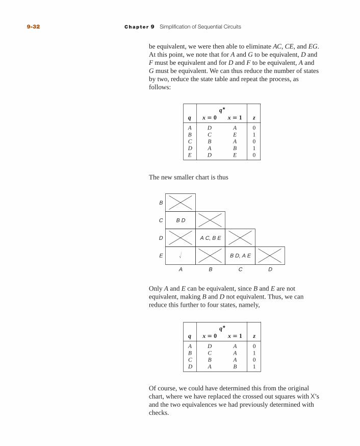
be equivalent, we were then able to eliminate AC, CE, and EG.At this point, we note that for A and G to be equivalent, D andF must be equivalent and for D and F to be equivalent, A andG must be equivalent. We can thus reduce the number of statesby two, reduce the state table and repeat the process, asfollows:
9-32 Chapter 9 Simplification of Sequential Circuits
Of course, we could have determined this from the originalchart, where we have replaced the crossed out squares with X’sand the two equivalences we had previously determined withchecks.
q�
q x � 0 x � 1 z
A D A 0B C E 1C B A 0D A B 1E D E 0
The new smaller chart is thus
Only A and E can be equivalent, since B and E are notequivalent, making B and D not equivalent. Thus, we canreduce this further to four states, namely,
B D
A C, B E
B
C
D
E B D, A E
BA C D
�
q�
q x � 0 x � 1 z
A D A 0B C A 1C B A 0D A B 1
mar91647_c09_000_000.qxd 11/24/08 12:08 PM Page 9-32
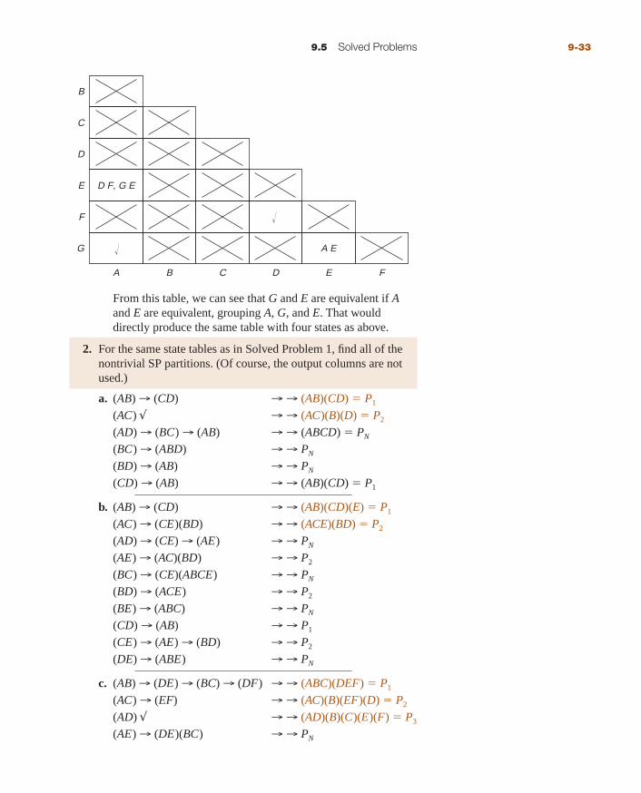
9.5 Solved Problems 9-33
From this table, we can see that G and E are equivalent if Aand E are equivalent, grouping A, G, and E. That woulddirectly produce the same table with four states as above.
2. For the same state tables as in Solved Problem 1, find all of thenontrivial SP partitions. (Of course, the output columns are notused.)
a. (AB) → (CD) → → (AB)(CD) � P1
(AC) √ → → (AC)(B)(D) � P2
(AD) → (BC) → (AB) →→ (ABCD) � PN
(BC) → (ABD) →→ PN
(BD) → (AB) →→ PN
(CD) → (AB) →→ (AB)(CD) � P1
b. (AB) → (CD) →→ (AB)(CD)(E) � P1
(AC) → (CE)(BD) →→ (ACE)(BD) � P2
(AD) → (CE) → (AE) →→ PN
(AE) → (AC)(BD) →→ P2
(BC) → (CE)(ABCE) →→ PN
(BD) → (ACE) →→ P2
(BE) → (ABC) →→ PN
(CD) → (AB) →→ P1
(CE) → (AE) → (BD) →→ P2
(DE) → (ABE) →→ PN
c. (AB) → (DE) → (BC) → (DF) →→ (ABC)(DEF) � P1
(AC) → (EF) →→ (AC)(B)(EF)(D) � P2
(AD) √ →→ (AD)(B)(C)(E)(F) � P3
(AE) → (DE)(BC) →→ PN
B
C
D
D F, G EE
F
G A E
BA C D E F
�
�
mar91647_c09_000_000.qxd 11/24/08 12:08 PM Page 9-33

(AF) → (DE)(AB) → (BC) →→ PN
(BC) → (DF)(AB)→ (ABC)(DEF) →→ P1
(BD) → (DE)(AB) → (BC) →→ PN
(BE) → (AC) → (EF) →→ (AC)(BEF)(D) � P4
(BF) → √ →→ (A)(BF)(C)(D)(E) � P5
(CD) → (EF)(AC) →→ (ACD)(B)(EF) � P6
(CF) → (DF)(AB) → (DE) →→ PN
(DE) → (BC) → (DF)(AB) →→ P1
(DF) → (DE)(AB) →→ P1
(EF) → (AC) →→ P2
At this point, we have found six SP partitions. We must nowadd each pair, since the sum of SP partitions is also SP. Theonly new partitions are
P3 � P4 � P7 � (ACD)(BEF)
P3 � P5 � P8 � (AD)(BF)(C)(E )
No new sums are formed from these two (since P7 is two-block). (We will return to this example in later solvedproblems.)
d. (AB) → (CD)(EG) → (ABEG)→ (CDF) →→ (ABEG)(CDF) � P1
(AC) → (BD) → (BE) → (CF) → (BDG) →→ PN
(AD) → (BG) → (CF)(AE) →→ PN
(AE) → (DF)(EG) → (AEG) →→ (AEG)(B)(C)(DF) � P2
(AF) → (BDG) → (ACF)(ABE) →→ PN
(AG) → (DF) →→ (AG)(B)(C)(DF)(E) � P3
(BC) → (GE) → (AE) → (DF) →→ (AEG)(BC)(DF) � P4
(BD) → (AC)(BE) →→ PN
(BE) → (CF) → (BG) → (AE) →→ P1
(BF) → (CG)(BE) → (BF)(AG) →→ PN
(BG) → (CF)(AE) → (DF)(EG) →→ P1
(CD) → (ABG) →→ P1
(CE) → (BF)(EG) →→ PN
(CF) → (BG) → (AE) → (DF)(EG) →→ P1
(CG) → (BF)(AG) →→ PN
(DE) → (AF)(BE) →→ PN
(DF) → (AG) →→ P3
(DG) → (ABF) →→ PN
(EF) → (FG)(BE) → (AB) →→ PN
9-34 Chapter 9 Simplification of Sequential Circuits
mar91647_c09_000_000.qxd 11/24/08 12:08 PM Page 9-34

(EG) → (AE) →→ P2
(FG) → (AB) →→ PN
The sums produce nothing new. Thus, there are four nontrivial SP partitions.
3. a. Reduce the system of Solved Problem 2a to one with aminimum number of states if the output column is
A (i) 0 (ii) 1 (iii) 0B 1 0 0C 0 0 1D 1 1 1
b. Reduce the system of Solved Problem 2c to one with aminimum number of states and find all of the SP partitions ofthe reduced system if the output column is
A (i) 0 (ii) 1 (iii) 0B 1 0 0C 0 1 1D 0 0 1E 0 0 1F 1 0 0
a. (i) P2 � (AC)(B)(D) is the only output consistent SPpartition. Thus, the system can be reduced to one withthree states:
9.5 Solved Problems 9-35
q�
q x � 0 x � 1 z
A A B 0B D A 1D B B 1
(ii) There are no output consistent SP partitions; therefore,the system cannot be reduced for this output column.
(iii) P1 � (AB)(CD) is the only output consistent SP partition.Thus, we can reduce the system to one with just twostates:
q�
q x � 0 x � 1 z
A C A 0C A A 1
mar91647_c09_000_000.qxd 11/24/08 12:08 PM Page 9-35

b. (i) The output consistent SP partitions are
P3 � (AD)(B)(C)(E)(F)
P5 � (A)(BF)(C)(D)(E)
P8 � (AD)(BF)(C)(E)
Clearly, P8 is larger than either of the others; it can beused to reduce the system to one with only four states.None of the SP partitions is larger than P8; therefore, thereduced system has no nontrivial SP partitions.
9-36 Chapter 9 Simplification of Sequential Circuits
(ii) The output consistent SP partitions are
P2 � (AC)(B)(D)(EF)
P4 � (AC)(BEF)(D)
P5 � (A)(BF)(C)(D)(E)
P4 is larger than either of the others and can be used toreduce this to a system with three states:
Since P7 � P4, then P7� � (AD)(B) is SP.
(iii) The only output consistent SP partition is
P5 � (A)(BF)(C)(D)(E)
Thus, the minimum system requires five states, namely,
q�
q x � 0 x � 1 z
A E B 0B A A 1C B B 0E A C 0
q�
q x � 0 x � 1 z
A B B 1B D A 0D B B 0
q�
q x � 0 x � 1 z
A E B 0B D A 0C B B 1D E B 1E D C 1
mar91647_c09_000_000.qxd 11/24/08 12:08 PM Page 9-36

There are three SP partitions for this reduced system,
P4� � (AC)(BE)(D)
P7� � (ACD)(BE)
P8� � (AD)(B)(C)(E)
4. Find good state assignments for each of the following statetables. (Each of the first four correspond to one of the statetables from Solved Problem 2.) Compute the input equations foreither D or JK flip flops and the output equation.
a. b.
c. d.
e.
f.
9.5 Solved Problems 9-37
q�
q x � 0 x � 1 z
A C B 0B D A 1C A B 0D B B 0
q�
q x � 0 x � 1 z
A C B 1B D A 1C A B 0D B B 1
q�
q x � 0 x � 1 z
A E B 0B D A 0C F B 1D E B 1E D C 1F D A 1
q�
q x � 0 x � 1 z
A E B 0B D A 0C F B 1D E B 1E D C 0F D A 1
q� zq x � 0 x � 1 x � 0 x � 1
A C D 0 0B E A 1 1C A D 0 0D B A 1 0E B C 1 1
q� zq x � 0 x � 1 x � 0 x � 1
A C D 0 1B E A 1 1C A D 0 0D B A 1 0E B C 1 1
mar91647_c09_000_000.qxd 11/24/08 12:08 PM Page 9-37

a. P2 � (AC)(B)(D) is output consistent; therefore, this systemcan be reduced to one with three states, namely,
9-38 Chapter 9 Simplification of Sequential Circuits
Since the other SP partition is not larger than P2, this systemhas no nontrivial SP partitions. There is not a good clue as tohow to choose partitions for a state assignment, other thanchoosing the output consistent one to minimize the outputlogic. We can try both
i. ii.
For assignment i, we get
D1 � x�q2 D2 � q1 � xq�2 z � q2
and for assignment ii, we obtain
D1 � x�q1 � xq�2 D2 � q1q�2 � xq�2 z � q2
The first assignment requires the least amount of logic. If wetried the third assignment, we would find that it needs aboutthe same amount of logic as the second (but uses 2 three-inputgates).
b. This, of course, is the same next state behavior as part a, butthe new output column is such that there are no outputconsistent SP partitions. We will implement it with JK flipflops. We do have one two-block SP partition,
P1 � (AB)(CD)
The two-block output consistent partition is not useful, sinceits product with P1 is not P0. We will use for the secondvariable
P3 � (AC)(BD)
which takes advantage of the other SP partition,P2 � (AC)(B)(D), by putting A and C in the same block. Thisresults in
J1 � x� K1 � 1 J2 � x K2 � xq�1 z � q�1 � q2
q�
q x � 0 x � 1 z
A A B 0B D A 1D B B 0
q q1 q2
A 0 0B 0 1D 1 0
q q1 q2
A 0 0B 1 1D 1 0
mar91647_c09_000_000.qxd 11/24/08 12:08 PM Page 9-38

Each of the other solutions requires very little logic as well.That will normally be the case with only two flip flops.
c. There are no output consistent SP partitions; thus, thissystem cannot be reduced. There are 2 two-block SPpartitions,
P1 � (ABC)(DEF)
P7 � (ACD)(BEF)
which will be used for the first two variables. The outputconsistent two-block partition is not useful, since its productwith P1 and P7 is not P0; states E and F would have the sameassignment. We need a partition to separate A from C and Efrom F. P3 indicates that A and D should be together; P5
indicates that B and F should be together. One of the partitionsthat accomplishes these goals and still produces a product ofP0 with P1 and P7 is
P9 � (ABDF)(CE)*
The resulting state assignment is
9.5 Solved Problems 9-39
*There are others; you should try them as an exercise to see if one of them produces aless costly solution.
The equations for q1 and q2 can be obtained from just theblock tables; the equation for D3 requires a 16-row truth tableand those for z require an 8-row table. (The work is left as anexercise for the reader.)
D1 � x� D2 � q�2 z � q1 � q3
D3 � x�q�2q�3 � {xq1q3 or xq2q3}
This solution requires four gates plus the NOT gate. If we usedthe straight binary assignment (A: 000, B: 001, . . .), we wouldneed 13 gates.
d. The next state portion of the table (and thus the list of SPpartitions) is the same as for part c. But, in this case, theproduct of the output consistent partition
POC � (ABE)(CDF)
q q1 q2 q3
A 0 0 0B 0 1 0C 0 0 1D 1 0 0E 1 1 1F 1 1 0
mar91647_c09_000_000.qxd 11/24/08 12:08 PM Page 9-39
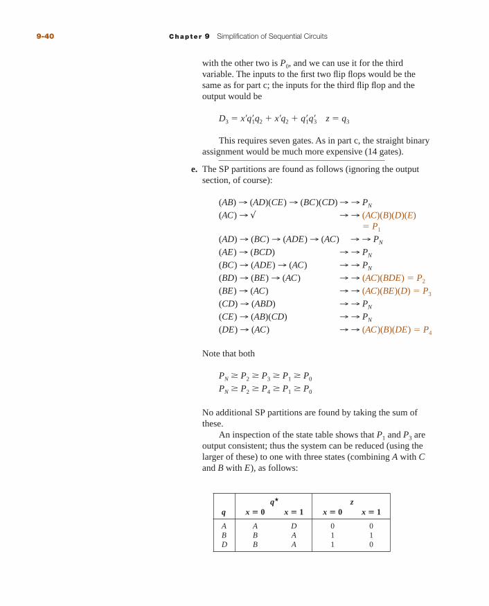
with the other two is P0, and we can use it for the thirdvariable. The inputs to the first two flip flops would be thesame as for part c; the inputs for the third flip flop and theoutput would be
D3 � x�q�1q2 � x�q2 � q�1q�3 z � q3
This requires seven gates. As in part c, the straight binaryassignment would be much more expensive (14 gates).
e. The SP partitions are found as follows (ignoring the outputsection, of course):
(AB) → (AD)(CE) → (BC)(CD) →→ PN
(AC) → √ →→ (AC)(B)(D)(E)� P1
(AD) → (BC) → (ADE) → (AC) →→ PN
(AE) → (BCD) →→ PN
(BC) → (ADE) → (AC) →→ PN
(BD) → (BE) → (AC) →→ (AC)(BDE) � P2
(BE) → (AC) →→ (AC)(BE)(D) � P3
(CD) → (ABD) →→ PN
(CE) → (AB)(CD) →→ PN
(DE) → (AC) →→ (AC)(B)(DE) � P4
Note that both
PN � P2 � P3 � P1 � P0
PN � P2 � P4 � P1 � P0
No additional SP partitions are found by taking the sum ofthese.
An inspection of the state table shows that P1 and P3 areoutput consistent; thus the system can be reduced (using thelarger of these) to one with three states (combining A with Cand B with E), as follows:
9-40 Chapter 9 Simplification of Sequential Circuits
q� zq x � 0 x � 1 x � 0 x � 1
A A D 0 0B B A 1 1D B A 1 0
mar91647_c09_000_000.qxd 11/24/08 12:08 PM Page 9-40

9.5 Solved Problems 9-41
Either directly from the state table or by converting it to a truthtable or directly to maps, we can determine
J1 � K1 � x
The first row of q� is the map for J and the second row is thatfor K�. (We can always do a block table for variables assignedusing SP partitions.)
There is no clue from the next state portion as to whichpartition to choose for the other variable. However, if we use
P4 � (AD)(B)
(which corresponds to the second column of the outputsection), we are assured of a fairly simple output equation,namely,
z � x�q1 � xq2
If we choose P4 for q2, then the state assignment and the truthtable for the next value of q2 and the output become
q�
q x � 0 x � 1
0(A) 0 11(B-D) 1 0
q x q1 q2 z q2�
A 0 0 0 0 0— 0 0 1 X XD 0 1 0 1 1B 0 1 1 1 1A 1 0 0 0 0— 1 0 1 X XD 1 1 0 0 0B 1 1 1 1 0
q q1 q2
A 0 0B 1 1D 1 0
The only SP partition for this reduced table is
P3� � (A)(BD)
It can be used for one variable, q1, in the state assignment. Forthat variable, we just need a next block table, namely,
mar91647_c09_000_000.qxd 11/24/08 12:08 PM Page 9-41

The maps for z and q2 (with the J portion for the quick methodshaded) are
The resulting equations are
z � q2 � x�q1 J2 � x�q1 K2 � x
Note that we have an even simpler version of z than expected.If we retain the SP partition for assigning the first variable
and use the other two-block partition, P5 � (AB)(D), for q2, weget
z � x�q2 � q1q�2 J2 � xq�1 K2 � 1
There is not much difference. Finally, if we do not use the SPpartition, but rather use the state assignment
0 1
00
01
11
10
x
z
q1 q2
11
XX
1
0 1
00
01
11
10
xq1 q2
1
XX
1
q2★
9-42 Chapter 9 Simplification of Sequential Circuits
we will get
z � q2 � x�q1 J1 � xq�2 K2 � 1 J2 � x�q1
K2 � x
For this simple problem, the state assignment does not make amajor difference.
f. The table of part f has one small change in the output section,so that there are no longer any output consistent SP partitions.We now need three variables, only one of which can use an SPpartition. The only two-block SP partition is P2, and we willuse it to assign q1. We will then use P3 to help with the secondvariable; it keeps A and C together, and B and E together. Wemust group D with AC; otherwise, we would just repeat the
q q1 q2
A 0 0B 0 1D 1 0
mar91647_c09_000_000.qxd 11/24/08 12:08 PM Page 9-42

same partition as before. Thus, we use
P5 � (ACD)(BE)
The product of these two is P3 and we must now find a two-block partition, the product of which with P3 is P0. There areseveral possibilities, such as
P6 � (ABD)(CE)
P7 � (AB)(CDE)
P8 � (AE)(BCD)
P9 � (ADE)(BC)
Any of these might lead to a good solution. Using P2, P5,and P6, we have the following state assignment and designtables:
9.5 Solved Problems 9-43
The block table is used to solve for q1 and the truth tableallows us to solve for the other two flip flop inputs and thesystem output. The resulting equations are
D1 � xq�1 � x�q1
D2 � x�q1
D3 � x�q�1q�3 � x�q2q�3 � {xq1q3 or xq2q3}
z � q2 � x�q1 � xq�1q�3
requiring nine gates (since x�q1 need only be built once) (plusa NOT gate to form x�).
q q1 q2 q3
A 0 0 0B 1 1 0C 0 0 1D 1 0 0E 1 1 1
x q1 q2 q3 q2� q3
� z
A 0 0 0 0 0 1 0C 0 0 0 1 0 0 0— 0 0 1 0 X X X— 0 0 1 1 X X XD 0 1 0 0 1 0 1— 0 1 0 1 X X XB 0 1 1 0 1 1 1E 0 1 1 1 1 0 1A 1 0 0 0 0 0 1C 1 0 0 1 0 0 0— 1 0 1 0 X X X— 1 0 1 1 X X XD 1 1 0 0 0 0 0— 1 1 0 1 X X XB 1 1 1 0 0 0 1E 1 1 1 1 0 1 1
q1�
q1 x � 0 x � 1
0 0 11 1 0
mar91647_c09_000_000.qxd 11/24/08 12:08 PM Page 9-43

we get the equations
D1 � x�q�2q3
D2 � xq�3 � q�1q�2q3
D3 � x�q1 � xq�1q�3 � q2q�3z � q1 � x�q3 � xq�2
This requires 11 gates (plus the NOT for x�), significantlymore logic than required for the other assignment. The otherassignments with P7, P8, and P9 are left as an exercise.
9.6 EXERCISES1. Reduce each of the following systems to ones with the minimum
number of states using the tabular method.
a. b.
�c.
d. Same table as c, except that the output for state B is 1.
9-44 Chapter 9 Simplification of Sequential Circuits
q q1 q2 q3
A 0 0 0B 0 0 1C 0 1 0D 0 1 1E 1 0 0
q�
q x � 0 x � 1 z
A C B 0B D A 0C A B 1D B B 1
q�
q x � 0 x � 1 z
A C B 0B D C 1C A B 0D A B 0
q�
q x � 0 x � 1 z
A C B 0B D A 0C E A 1D E B 1E D B 1
If, instead, we used the assignment (just the first fivebinary numbers)
EX
ER
CIS
ES
mar91647_c09_000_000.qxd 11/24/08 12:08 PM Page 9-44

g.
�h.
i. j.
�k. l.
9.6 Exercises 9-45
q�
q x � 0 x � 1 z
A B C 0B D E 1C D F 0D B E 1E F C 0F D A 0
q�
q x � 0 x � 1 z
A E B 0B C C 1C D E 1D F B 0E A F 1F D F 1
q�
q x � 0 x � 1 z
A B G 0B A E 1C A F 1D G B 1E C D 0F B D 0G G B 1
q� zq x � 0 x � 1 x � 0 x � 1
A B D 0 0B E G 1 0C G F 0 0D A C 1 1E B D 0 0F G D 0 0G A B 1 0
q�
q x � 0 x � 1 z
A G B 0B E C 0C E B 1D A B 0E F D 0F E D 1G A B 1
q�
q x � 0 x � 1 z
A G B 0B E C 1C E B 1D A B 1E F D 1F E D 1G A B 0
q�
q x � 0 x � 1 z
A F B 0B E C 0C D C 1D C A 0E B C 1F A B 0
e. f.q�
q x � 0 x � 1 z
A B B 0B F D 0C D A 1D C E 0E F E 0F E A 1
EX
ER
CIS
ES
mar91647_c09_000_000.qxd 11/24/08 12:08 PM Page 9-45

2. For each of the state tables of Exercise 1, find all of the nontrivialSP partitions.
3. a. For state tables a and b of Exercise 2, reduce the system to onewith a minimum number of states if the output column is
A (i) 0 (ii) 1 (iii) 0 (iv) 0
B 1 0 0 1
C 0 0 1 0
D 1 1 1 0
b. Reduce the system of Exercises 1e and 1g to ones with aminimum number of states if the output column is
A (i) 0 (ii) 1 (iii) 0 (iv) 1
B 1 0 0 0
C 0 1 0 0
D 1 1 1 0
E 0 0 1 0
F 1 1 1 0
�c. Reduce the system of Exercises 1k to one with a minimumnumber of states if the output column is
A (i) 0 (ii) 1 (iii) 0 (iv) 1
B 1 0 0 0
C 1 1 1 0
D 1 1 1 1
E 0 0 1 0
F 0 1 0 0
G 0 1 0 1
4. a. For Solved Problem 4c,
i. Find the D’s and z for the straight binary assignment.
ii. Find D3 and z using the two SP partitions for q1 and q2
and using P9 � (ABDE) (CF) for q3.
iii. Find D3 and z using the two SP partitions for q1 and q2
and using P10 � (ADE) (BCF) for q3.
b. Continue the example of Solved Problem 4f, using
P2 � (AC)(BDE )
P5 � (ACD)(BE )
and each of
i. P7 � (AB)(CDE )
ii. P8 � (AE)(BCD)
iii. P9 � (ADE)(BC)
9-46 Chapter 9 Simplification of Sequential Circuits
EX
ER
CIS
ES
mar91647_c09_000_000.qxd 11/24/08 12:08 PM Page 9-46

5. For each of the state tables shown below, find a good stateassignment and design the system using JK flip flops. Comparethat design with the state assignment that just uses the binarynumbers in order for the states (that is, A: 000, B: 001,C: 010, . . .).*
a.
b.
�c. Exercise 1e with output d. Exercise 1k.
column 1
0
0
1
1
0
6. For each of the following output columns, reduce the system ifpossible and find a good state assignment
9.6 Exercises 9-47
*Note that part b has the same next state portion as Solved Problem 2d.
q�
q x � 0 x � 1 z
A D B 1B C D 1C E D 1D A B 0E C D 0
q� zq x � 0 x � 1 x � 0 x � 1
A D G 1 0B C E 1 1C B G 0 1D A B 0 0E F E 1 0F G B 1 1G F A 1 1
q�
q x � 0 x � 1 z1 z2 z3 z4
A E B 0 0 1 0B C D 0 0 0 0C E F 1 1 0 0D E A 1 0 0 1E C F 0 1 0 1F C D 1 0 1 0
EX
ER
CIS
ES
mar91647_c09_000_000.qxd 11/24/08 12:08 PM Page 9-47

9.7 CHAPTER 9 TEST (50 MINUTES)1. Using the techniques of Section 7.1, reduce the following state
table to one with the minimum number of states.
9-48 Chapter 9 Simplification of Sequential Circuits
2. For the state table of Problem 1,
a. For each of the following partitions, indicate whether or not itis SP and whether or not it is output consistent.
P1 � (ABCD)(E)
P2 � (ABE)(CD)
P3 � (AC)(BE)(D)
P4 � (AB)(CD)(E)
P5 � (AB)(CDE)
P6 � (A)(B)(C)(D)(E)
b. Using one of these partitions, reduce the system to theone with the smallest number of states, showing a new statetable.
q� zq x � 0 x � 1 x � 0 x � 1
A 0 0B 0 1C 1 1D 0 0E 1 1F 1 0
q�
q x � 0 x � 1 z
A C B 0B D A 0C E A 0D E B 0E D B 1
7. Consider the following state table, where the next state is notspecified. Complete the next state portion such that the system canbe reduced to four states (not any smaller) and it is possible toget from any state to any other state with an appropriate inputsequence.
EX
ER
CIS
ES
CH
AP
TE
R T
ES
T
mar91647_c09_000_000.qxd 11/24/08 12:08 PM Page 9-48
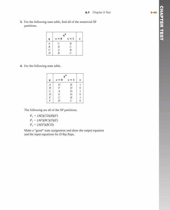
3. For the following state table, find all of the nontrivial SPpartitions.
9.7 Chapter 9 Test 9-49
4. For the following state table,
q�
q x � 0 x � 1 z
A D B 1B F D 0C A D 1D E D 0E C B 1F D C 0
q�
q x � 0 x � 1 z
A C BB D CC A BD B C
The following are all of the SP partitions,
P1 � (AE)(CD)(B)(F)
P2 � (AF)(BC)(D)(E)
P3 � (AEF)(BCD)
Make a “good” state assignment and show the output equationand the input equations for D flip flops.
CH
AP
TE
R T
ES
T
mar91647_c09_000_000.qxd 11/24/08 12:08 PM Page 9-49

AA P P E N D I X
Relating the Algebrato the Karnaugh Map
Although we use the map without worrying about the algebra, it isuseful to see how some of the properties appear on the map.
Property 9a. ab + ab�� = a
On the left, we have circled w�x and wx. They combine to form the termx. Two adjacent rectangles combine to form one larger rectangle. Another geometry is shown next.
Here, w�y + wy = y.
00 01 11 10
0
1
w x
y
1
1
1
1
00 01 11 10
0
1
w x
y
1
1
1
1
00 01 11 10
0
1
w x
y
11 1 1 11 1 1
00 01 11 10
0
1
w x
y
543
mar91647_apa_543_547.qxd 12/2/08 11:22 AM Page 543

544 Append ix A Relating the Algebra to the Karnaugh Map
where y�z + w�xyz = y�z + w�xz. After factoring out the common z, wehave z (y� + yw�x). Thus, the a of P10 is y�, and the b is w�x.
Property 12a. a + ab = a
where the term xy on the left map is completely contained in the term y,and can thus be deleted.
Property 10a. a + a��b = a + b
00 01 11 10
0
1
w x
y
1
1
1 1
1
1
00 01 11 10
0
1
w x
y
On the left, we have w�y and w�xy�. Algebraically, we would factor w�from both terms, leaving w� (y + xy�) = w� (y + y�x). For Property 10a, ais y, and b is x. Thus, we have w�y + w�x, as shown on the right map. Onthe map, this involves one group adjacent to a smaller group. A four-variable example is shown below.
00 01 11 10
00
01
11
10
w x
y z
1
1
11 1
00 01 11 10
00
01
11
10
w x
y z
1
1
11 1
00 01 11 10
0
1
w x
y
11 1 1 11 1 1
00 01 11 10
0
1
w x
y
mar91647_apa_543_547.qxd 12/2/08 11:22 AM Page 544

Append ix A Relating the Algebra to the Karnaugh Map 545
Property 13a. at1 + a��t2 + t1t2 = at1 + a��t2
00 01 11 10
0
1
w x
y
1
1
1
1
00 01 11 10
0
1
w x
y
1
1
1
1
The term wx on the left map is the consensus of xy� and wy, and is thusremoved on the right map. The 1’s of the consensus term are half fromone group and half from the other. A larger example is shown next,
where wy�z is the consensus of xz and wx�y� and has been removed on theright map.
We will now look at some examples of algebraic reduction, showingthe corresponding maps.
Reduce the following to two terms with four literals.
f = wxy� + yz + xz + w�xy� + w�xy�z�
The function is shown on the first map. After using Property 9a on the first andfourth term and Property 12a on the last two terms, we get the second map.
00 01 11 10
00
01
11
10
w x
y z
1
1
1
1
1 1
1
00 01 11 10
00
01
11
10
w x
y z
1
1 1
11 1
1
11 1 1
00 01 11 10
00
01
11
10
w x
y z
11
11
00 01 11 10
00
01
11
10
w x
y z
11
1
1 1
1
11
11 1 1
00 01 11 10
00
01
11
10
w x
y z
11
11
EXAMPLE A.1
mar91647_apa_543_547.qxd 12/3/08 4:29 PM Page 545

546 Append ix A Relating the Algebra to the Karnaugh Map
f = xy� + xz + yz
But xz is the consensus of xy� and yz, producing
f = xy� + yz
and the third map.
Reduce the following to three terms and seven literals.
G = BC + AC�D + AB�D + A�C�D�
This function is plotted on the first map.
EXAMPLE A.2
00 01 11 10
00
01
11
10
A B
C D
1
1
1
1
1
1
1 1 1 1
1
1
00 01 11 10
00
01
11
10
A B
C D
1 1 1
1 1
1 1
The consensus of the first two terms gives us ABD, as shown on the sec-ond map. Property 9a then allows us to replace AB�D + ABD by AD (asshown on the next map) and Property 12a allows us to remove AC�D, finallyreducing the expression to
G = BC + AD + A�C�D�
00 01 11 10
00
01
11
10
A B
C D
1
1
1
1
1
1
1 1 1 1
1
1
00 01 11 10
00
01
11
10
A B
C D
1 1 1
1 1
1 1
mar91647_apa_543_547.qxd 12/2/08 11:22 AM Page 546

Append ix A Relating the Algebra to the Karnaugh Map 547
h = wx + wz + w�xz� + x�yz + w�yz�
The first map shows the original terms. Using Property 10a on the first andthird terms produces xz�. Then, wx ¢ xz� = wx and allows us to remove thatterm, producing the second map.
h = wz + xz� + x�yz + w�yz�
Reduce the following to three terms and seven literals. EXAMPLE A.3
00 01 11 10
00
01
11
10
w x
y z
1 1
11
1 1 1
1 11
00 01 11 10
00
01
11
10
w x
y z
1 1
11
1 1 1
1 11
None of the properties other than consensus help, and the only consensusthat exists is
x�yz ¢ w�yz� = w�x�y
If we add that term, as on the next map, we can then compute
00 01 11 10
00
01
11
10
w x
y z
1 1
11
1 1 1
1 11
00 01 11 10
00
01
11
10
w x
y z
1 1
11
1 1 1
1 11
wz ¢ w�x�y = x�yz and xz� ¢ w�x�y = w�yz�
Thus, we can remove x�yz and w�yz�, leaving
h = wz + xz� + w�x�y
as shown on the fourth map.
mar91647_apa_543_547.qxd 12/2/08 11:22 AM Page 547

B.1 Chapter 1 Answers1. a. 31 d. 47 h. 02. a. 000001001001
e. 001111101000g. 4200 � 212 � 4096 Thus, can’t represent in 12 bits
3. a. 96Bc. 317
4. c. 10235. a. 001111 3 � 12 � 15
d. 000001 51 � 14 � 65 overflowe. 110010 11 � 39 � 50
6. a. 011001 c. cannot be storede. 110001
7. c. �21 d. �28 h. �328. c. 10001111
d. cannot store numbers larger than �1279. a. 000100 �11 � (�15) � �4
d. 010000 �22 � (�26) � overflowf. 101101 �3 � (�16) � �19
10. b. 111001 i. 17 � 24 � overflowii. � 17 � (�24) � �7
c. 110011 i. 58 � 7 � 51ii. �6 � (�7) � �13
d. 001100 i. 36 � 24 � 12ii. �28 � (�24) � overflow
11. a. i. 0001 0000 0011ii. 0001 0000 0011
iii. 0001 0000 0011iv. 0100 0011 0110v. 10100 11000 10001
12. i. ii. iii. iv. v. vi.b. no 18 15 no 27 �27d. 95 no no 62 149 �107
13. a. ii. 0100010 1001111 1001011 0100010b. iii. 9/3 � 3
APPENDIX B: ANSWERS TO SELECTED EXERCISES
AP
PE
ND
IX B
: A
NS
WE
RS
TO
SE
LE
CT
ED
EX
ER
CIS
ES
548
mar91647_apba_548_555.qxd 12/2/08 9:43 AM Page 548
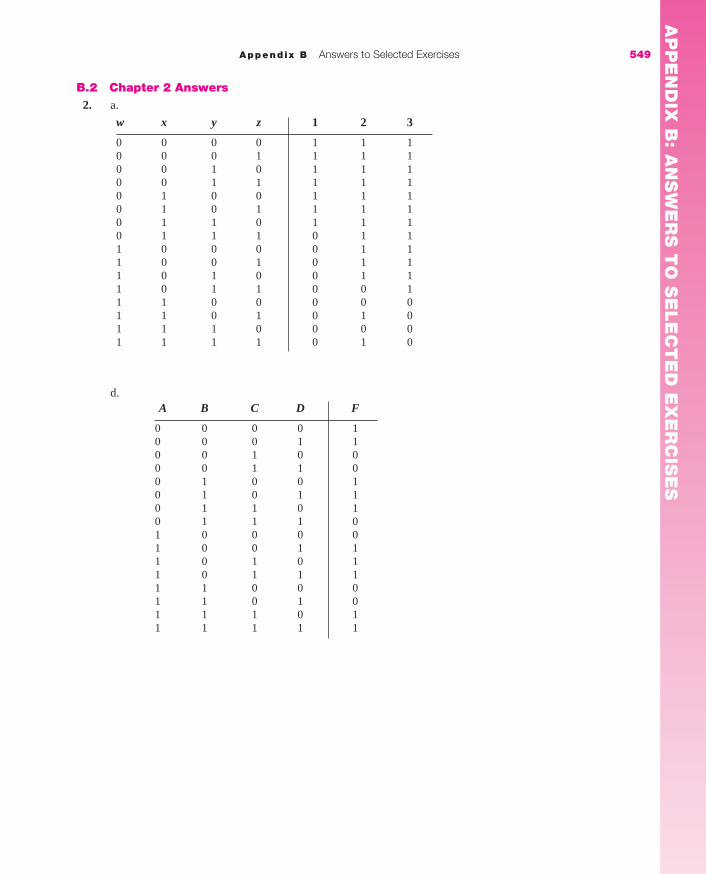
Append ix B Answers to Selected Exercises 549
B.2 Chapter 2 Answers2. a.
w x y z 1 2 3
0 0 0 0 1 1 10 0 0 1 1 1 10 0 1 0 1 1 10 0 1 1 1 1 10 1 0 0 1 1 10 1 0 1 1 1 10 1 1 0 1 1 10 1 1 1 0 1 11 0 0 0 0 1 11 0 0 1 0 1 11 0 1 0 0 1 11 0 1 1 0 0 11 1 0 0 0 0 01 1 0 1 0 1 01 1 1 0 0 0 01 1 1 1 0 1 0
A B C D F
0 0 0 0 10 0 0 1 10 0 1 0 00 0 1 1 00 1 0 0 10 1 0 1 10 1 1 0 10 1 1 1 01 0 0 0 01 0 0 1 11 0 1 0 11 0 1 1 11 1 0 0 01 1 0 1 01 1 1 0 11 1 1 1 1
d.
AP
PE
ND
IX B
: AN
SW
ER
S T
O S
ELE
CT
ED
EX
ER
CIS
ES
mar91647_apba_548_555.qxd 12/2/08 9:43 AM Page 549

5. b. f � h, but � g because of row 0116. b. ii. sum of three product terms
d. iv. product of two sum termsf. i. product of 1 literal iii. sum of 1 literal
ii. sum of 1 product term iv. product of 1 sum termg. none
7. b. 4 d. 3 f. 1 g. 68. a. � z
d. � a�b� � acf. � x�y�� x�z � xy
also � x�y� � yz � xy9. c. (a � c�) (a�� c) (a�� b�) � (a� c�) (a�� c) (b�� c�)
550 Append ix B Answers to Selected Exercises
X Y Z F
0 0 0 10 0 1 00 1 0 10 1 1 11 0 0 11 0 1 01 1 0 01 1 1 1
a b c d g
0 0 0 0 10 0 0 1 00 0 1 0 10 0 1 1 00 1 0 0 10 1 0 1 00 1 1 0 10 1 1 1 11 0 0 0 01 0 0 1 11 0 1 0 01 0 1 1 11 1 0 0 X1 1 0 1 X1 1 1 0 X1 1 1 1 X
g.
3. a.
4. a.
b
c
a
a
b
c
AP
PE
ND
IX B
: A
NS
WE
RS
TO
SE
LE
CT
ED
EX
ER
CIS
ES
mar91647_apba_548_555.qxd 12/2/08 9:43 AM Page 550

Append ix B Answers to Selected Exercises 551
11. c. i. h � a�c(b � d) � a (c� � bd)ii. � a�bc � a�cd � ac� � abd
12. a. f � � (a�� b�� d)(b� c)(a� c�� d�)(a� b�� c� d�)14. a. f (a, b, c) � �m(1, 5, 6, 7)
g(a, b, c) � �m(0, 1, 4, 5, 6)b. f � a�b�c � ab�c � abc� � abc
g � a�b�c� � a�b�c � ab�c� � ab�c � abc�
c. f � b�c � abg � b� � ac�
d. f �(a, b, c) � �m(0, 2, 3, 4)g�(a, b, c) � �m(2, 3, 7)
e. f � (a � b � c)(a � b� � c) (a � b� � c�)(a� � b � c)g � (a � b� � c)(a � b� � c�)(a� � b� � c�)
f. f � (b � c)(a � b�)g � (a � b�)(b� � c�)
16. a. yes b. no c. yes d. no e. no f. yes18. a. f � a(bc)� � (c � d�)� � ab� � ac� � c�d
e. f � 1 � (ab � cd) � a�c� � a�d� � b�c� � b�d�
x
y
z
vw
10. c.
AP
PE
ND
IX B
: AN
SW
ER
S T
O S
ELE
CT
ED
EX
ER
CIS
ES
mar91647_apba_548_555.qxd 12/2/08 9:43 AM Page 551

19. d.
552 Append ix B Answers to Selected Exercises
20. c. f � b � a�c21. c. F � W�Z� � Y�Z � WXY
e. G � B�D � BC � A�Dg. g � bc�d � abc � a�bd�
� a�bc� � abd � bcd�
22. a. f � a�b�c� � a�bd � a�cd� � abc � a�c�d� a�b�d� � a�bc � bcd � bcd�
� bc � a�c�d � a�b�d�
23. b. g � x�y�z� � x�y�z � x�yz� � x�yz � xyz � xy�z�
g(w, x, y, z) � �m(0, 1, 2, 3, 4, 7)24. c. xy � w�z25. c. (b� � d)(c � d)(a� � b � d �)(b� � c� � d�)26. a. f � w(y� � xz�) � z(y� � w�x�)
F
B�
B�
C�
A�
C�
E�
A
A
A
D
D�B
E
E
x
y
w
z
f
y
x�
w�
z�
AP
PE
ND
IX B
: A
NS
WE
RS
TO
SE
LE
CT
ED
EX
ER
CIS
ES
mar91647_apba_548_555.qxd 12/2/08 9:43 AM Page 552
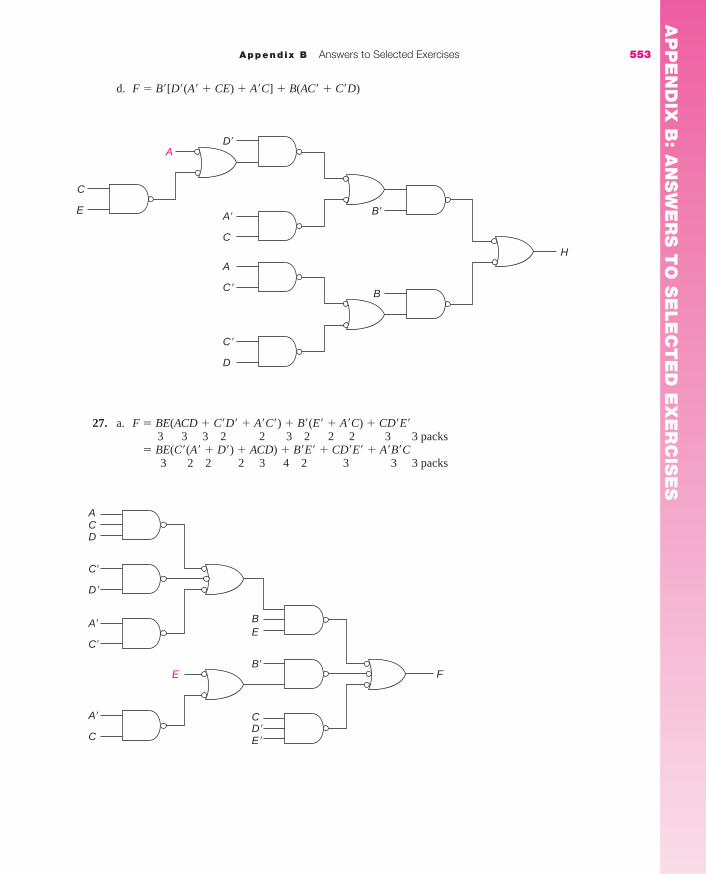
Append ix B Answers to Selected Exercises 553
27. a. F � BE(ACD � C�D� � A�C�) � B�(E� � A�C) � CD�E�3 3 3 2 2 3 2 2 2 3 3 packs
� BE(C�(A� � D�) � ACD) � B�E� � CD�E� � A�B�C3 2 2 2 3 4 2 3 3 3 packs
d. F � B�[D�(A� � CE) � A�C] � B(AC� � C�D)
A�
D�
C
C
A
E
B
H
C�
B�
D
A
C�
B�
C�
F
A
D
BE
E
C
C
D�
D�
A�
C�
A�
C E�
AP
PE
ND
IX B
: AN
SW
ER
S T
O S
ELE
CT
ED
EX
ER
CIS
ES
mar91647_apba_548_555.qxd 12/2/08 9:43 AM Page 553

B.3 Chapter 3 Answers1. b.
554 Append ix B Answers to Selected Exercises
00 01 11 10
00
01
11
10
w x
y z
XX
X1
1 1
1
1
11
00 01 11 10
00
01
11
10
a b
c d
1
1
1
1 1
1
1
1
1
1
c.
2. b. g � w�x� � wx � wy g � w�x� � wx � x�ye. G � X�Z� � W�XZ � WXY�
i. h � pq � qr� � r�s� � p�q�r � prsh � pq � qr� � r�s� � p�q�r � q�rsh � pq � qr� � r�s� � q�rs � p�q�s�
l. Prime Implicants: xy, yz, xz, wz, w�x, w�y�z�, x�y�z�, wx�y�
Minimum: g � yz � xy � w�x � wz � x�y�z�
m. H � X�Z� � W�X�Y � W�XZ � WXY�
H � X�Z� � W�YZ � W�XZ � WXY�
H � X�Z� � W�YZ � XY�Z � WXY�
H � X�Z� � W�YZ � XY�Z � WY�Z�
n. f � a�c� � ab� � cd� � bdf � b�c�� a�b � cd� � adf � c�d � ac � a�b � b�d�
f � a�c� � ad � bc � b�d�
f � b�c� � bd � ac � a�d�
f � c�d � bc � ab� � a�d�
AP
PE
ND
IX B
: A
NS
WE
RS
TO
SE
LE
CT
ED
EX
ER
CIS
ES
mar91647_apba_548_555.qxd 12/2/08 9:43 AM Page 554
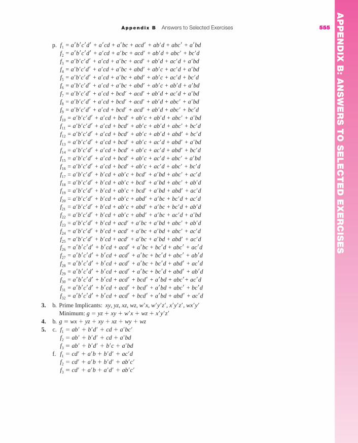
Append ix B Answers to Selected Exercises 555
p. f1 = a�b�c�d� + a�cd + a�bc + acd� + ab�d + abc� + a�bdf2 = a�b�c�d� + a�cd + a�bc + acd� + ab�d + abc� + bc�df3 = a�b�c�d� + a�cd + a�bc + acd� + ab�d + ac�d + a�bdf4 = a�b�c�d� + a�cd + a�bc + abd� + ab�c + ac�d + a�bdf5 = a�b�c�d� + a�cd + a�bc + abd� + ab�c + ac�d + bc�df6 = a�b�c�d� + a�cd + a�bc + abd� + ab�c + ab�d + a�bdf7 = a�b�c�d� + a�cd + bcd� + acd� + ab�d + ac�d + a�bdf8 = a�b�c�d� + a�cd + bcd� + acd� + ab�d + abc� + a�bdf9 = a�b�c�d� + a�cd + bcd� + acd� + ab�d + abc� + bc�df10 = a�b�c�d� + a�cd + bcd� + ab�c + ab�d + abc� + a�bdf11 = a�b�c�d� + a�cd + bcd� + ab�c + ab�d + abc� + bc�df12 = a�b�c�d� + a�cd + bcd� + ab�c + ab�d + abd� + bc�df13 = a�b�c�d� + a�cd + bcd� + ab�c + ac�d + abd� + a�bdf14 = a�b�c�d� + a�cd + bcd� + ab�c + ac�d + abd� + bc�df15 = a�b�c�d� + a�cd + bcd� + ab�c + ac�d + abc� + a�bdf16 = a�b�c�d� + a�cd + bcd� + ab�c + ac�d + abc� + bc�df17 = a�b�c�d� + b�cd + ab�c + bcd� + a�bd + abc� + ac�df18 = a�b�c�d� + b�cd + ab�c + bcd� + a�bd + abc� + ab�df19 = a�b�c�d� + b�cd + ab�c + bcd� + a�bd + abd� + ac�df20 = a�b�c�d� + b�cd + ab�c + abd� + a�bc + bc�d + ac�df21 = a�b�c�d� + b�cd + ab�c + abd� + a�bc + bc�d + ab�df22 = a�b�c�d� + b�cd + ab�c + abd� + a�bc + ac�d + a�bdf23 = a�b�c�d� + b�cd + acd� + a�bc + a�bd + abc� + ab�df24 = a�b�c�d� + b�cd + acd� + a�bc + a�bd + abc� + ac�df25 = a�b�c�d� + b�cd + acd� + a�bc + a�bd + abd� + ac�df26 = a�b�c�d� + b�cd + acd� + a�bc + bc�d + abc� + ac�df27 = a�b�c�d� + b�cd + acd� + a�bc + bc�d + abc� + ab�df28 = a�b�c�d� + b�cd + acd� + a�bc + bc�d + abd� + ac�df29 = a�b�c�d� + b�cd + acd� + a�bc + bc�d + abd� + ab�df30 = a�b�c�d� + b�cd + acd� + bcd� + a�bd + abc�+ ac�df31 = a�b�c�d� + b�cd + acd� + bcd� + a�bd + abc� + bc�df32 = a�b�c�d� + b�cd + acd� + bcd� + a�bd + abd� + ac�d
3. b. Prime Implicants: xy, yz, xz, wz, w�x, w�y�z�, x�y�z�, wx�y�
Minimum: g � yz � xy � w�x � wz � x�y�z�
4. b. g � wx � yz � xy � xz � wy � wz5. c. f1 � ab� � b�d� � cd � a�bc�
f2 � ab� � b�d� � cd � a�bdf3 � ab� � b�d� � b�c � a�bd
f. f1 � cd� � a�b � b�d� � ac�df2 � cd� � a�b � b�d� � ab�c�
f3 � cd� � a�b � a�d� � ab�c�
AP
PE
ND
IX B
: AN
SW
ER
S T
O S
ELE
CT
ED
EX
ER
CIS
ES
mar91647_apba_548_555.qxd 12/16/08 2:44 PM Page 555

6. c. All are different.f. f2 and f3 are equal; f1 treats m13 differently
7. a. f � A�B � C�D � ADf � (B � D)(A � B � C�) (A� � D)
d. f1 � a�d� � ad � bc � abf2 � a�d� � ad � bc � bd�
f3 � (a� � b � d )(a � c � d�)(a � b � d�)i. f1 � w�z � wy � xz
f2 � w�z � wy � wxf3 � w�z � wx � x�zf4 � w�z � wx � yzf5 � w�x� � wx � yzf6 � w�x� � wy � xzf7 � (w � z)(w� � x � y)
8. a, d. Since there are no don’t cares, all solutions to each problem areequal.
i. All are different.9. c. H � AB�E � BD�E� � BCDE � A�CD�E
f. H � V�W�Z � V�WY � VWY� � W�X�Z� � VWXZH � V�W�Z � V�WY � VWY� � W�X�Z� � WXYZ
i. H � A�C�D� � CDE� � B�CE � AD�E � {ACD� or ACE�}H � A�C�D� � CDE� � B�CE � ACD� � C�D�E
n. G � X�Y� � V�XZ � {VWZ or WXZ}10. b. G � B�C�E�F� � BD�F � AB�C�D� � CDEF� � A�B�C�E
� ABF � BC�F � A�BCDE�
11. a. f � a�b�d � ab�c� � bc�d � acd�
g � a�b � bc�d � acd�
e. F � WY � WZ� � W�XZ � W�X�Y�ZG � Y�Z� � W�XY � W�X�Y�Z
h. f � c�d� � a�cd � bdg � bd � a�c�d � ab� � {abc or acd�}h � b�cd� � bd � a�c�d � a�bc� � {abc or acd�}
j. f � b�c�d � a�b� � a�c�d� orf � b�c�d � a�b�� bc�d� orf � b�c�d � b�c � a�c�d�
g � b�c�d � cd�
12. b. F � A�B�C�D � AC�D� � ACD � BCD� � A�BCDG � A�B�C�D� � BCD� � A�BCDH � AC�D� � AD � A�BCD � A�B�C�D�
F � A�B�C�D � AC�D� � ACD � BCD� � A�BCDG � A�B�C�D� � BCD� � A�BCDH � ACD � AC� � A�BCD � A�B�C�D�
AP
PE
ND
IX B
: A
NS
WE
RS
TO
SE
LE
CT
ED
EX
ER
CIS
ES
556 Append ix B Answers to Selected Exercises
mar91647_apbb_556_572.qxd 12/2/08 11:30 AM Page 556

B.4 Chapter 4 Answers1., 2. b. w�x� d. r�s� f. a�b h. V�W�X�
wx qr� b�d� W�X�Z�
x�y pq cd� V�W�Zwy p�q�s� a�c V�YZ
p�q�r a�d� V�WYprs ac�d V�X�Yq�rs bc�d VX�Y�Z�
ab�c� VWY�
VWXZWXYZ
3. b. g � w�x� � wx � wyg � w�x� � wx � x�y
d. h � pq � qr� � r�s� � p�q�r � prsh � pq � qr� � r�s� � p�q�r � q�rsh � pq � qr� � r�s� � q�rs � p�q�s�
f. f1 � cd� � a�b � b�d� � ac�df2 � cd� � a�b � b�d� � ab�c�
f3 � cd� � a�b � a�d� � ab�c�
h. H � V�W�Z � V�WY � VWY� � W�X�Z� � VWXZH � V�W�Z � V�WY � VWY� � W�X�Z� � WXYZ
4., 5. b. Prime implicants of F: W�Y�Z, XYZ, WY, WZ�, W�XZPrime implicants of G: Y�Z�, W�X�Y�, W�XY, W�XZ�
Shared terms: W�XYZ, W�X�Y�Z, WY�Z�
d. Terms for f only: a�cd, c�d�, bc�
Terms for g only: c�d, ab�, ac, adTerm for h only: b�cd�
Term for f and g: ab�c�d�
Term for f and h: a�bc�
Terms for g and h: a�c�d, abc, acd�
Term for all three: bd6. b. F � WY � WZ� � W�XZ � W�X�Y�Z
G � Y�Z� � W�XY � W�X�Y�Zd. f � c�d� � a�cd � bd
g � bd � a�c�d � ab� � {abc or acd�}h � b�cd� � bd � a�c�d � a�bc� � {abc or acd�}
AP
PE
ND
IX B
: AN
SW
ER
S T
O S
ELE
CT
ED
EX
ER
CIS
ES
Append ix B Answers to Selected Exercises 557
mar91647_apbb_556_572.qxd 12/2/08 11:30 AM Page 557

558 Append ix B Answers to Selected Exercises
B.5 Chapter 5 Answers2. a. The truth table for this module is
a b c y s t
0 0 0 0 1 00 0 1 0 1 10 1 0 0 1 10 1 1 1 0 01 0 0 1 0 01 0 1 1 0 11 1 0 1 0 11 1 1 1 1 0
a b c X Y
0 0 0 0 00 0 1 0 10 1 0 0 00 1 1 1 11 0 0 0 01 0 1 1 11 1 0 1 01 1 1 1 1
y � a � bc s � a�b� � a�c� � abc t � b�c � bc�
b. The delay from c to y is 2 for each module. The total delay is 32 � 1.
7.
0123
b
c
0123
s
cout
EN�a
EN�a�
9.
AP
PE
ND
IX B
: A
NS
WE
RS
TO
SE
LE
CT
ED
EX
ER
CIS
ES
mar91647_apbb_556_572.qxd 12/2/08 11:30 AM Page 558

x
y
y
f
0
1
z
0
1
0
1
1
1
12.
Y
A
A�
B
D�C
A
B�
C�
Z
D�
D�
AB
A�B�C�D� X
BC
D
B�
D�C
18. a.
AP
PE
ND
IX B
: AN
SW
ER
S T
O S
ELE
CT
ED
EX
ER
CIS
ES
Append ix B Answers to Selected Exercises 559
mar91647_apbb_556_572.qxd 12/2/08 11:30 AM Page 559

560 Append ix B Answers to Selected Exercises
*Solving X7 alone, you would use BD� in place of A�CD�. But, the latter is also a primeimplicant and can be shared, saving one gate and three inputs. Gate count is based on BD�.
b. The solution is straightforward; the diagram is not shown.c. We need two decoders. A is connected to the enable of the first. The
outputs correspond to the first eight minterms. A� is used to enable thesecond, producing the other eight minterms. Only three OR gates areneeded.
d. The solution of part a is implemented on a PLA with seven terms:
X � ABD1 � A�B�C�D�2 � A�BC3 � BCD�4 � B�CD�5Y � AC�D� � ABD1 � A�BC3 � B�CD�5Z � ABD1 � A�B�C�D�2 � AB�D� � BCD�4
e. The PAL would be implemented with a solution using only primeimplicants of individual functions:
X � A�B�D� � CD� � ABD � BCY � AC�D� � ABD � A�BC � B�CD� or
� A�CD� � BCD � ABC� � AB�D�
Z � B�C�D� � ABD � BCD� � {AB�D� � ACD�}
21. a. X1 � B�D�2 � BD � AC�1 � A�CX2 � B� � C�D� � AD� � AC�1 � A�CDX3 � D � B�C� � A�B � AC4 ***or
� D � A�C� � BC � AB�
X4 � B�D�2 � A�B�C5 � A�CD�6 � BC�D � ABD � AC�1X5 � B�D�2 � A�CD�6 � AC�D�
X6 � A�BC� � ABC � AB�C� � {B�C�D� or A�C�D�}� {ACD� or AB�D�} � {BCD� or A�BD�}
X7 � BC� � AC�1 � AB3 � A�B�C5 � {A�CD�6* or BD�}X8 � AB7 � AC3
Package Count
X1: 2 2 2 2 4X2: 0 2 2 (2) 3 5X3: 0 2 2 2 4X4: (2) 3 3 3 3 (2) 6X5: (2) (3) 3 3X6: 3 3 3 3 3 3 6X7: 2 (2) 2 (3) 2 5X8: (2) (2) 2
2’s: 13 7430s: 4 32 gates/95 inputs3’s: 13 7420s: 14’s: 2 7410s: 5 (2 left over)5’s: 2 7400s: 3 (use one 3-input)6’s: 2 Total: 13 packages
AP
PE
ND
IX B
: A
NS
WE
RS
TO
SE
LE
CT
ED
EX
ER
CIS
ES
mar91647_apbb_556_572.qxd 12/2/08 11:30 AM Page 560

00
0 1
1
1
1
C0
D1
A1
B0
0
b. X1 � B�D�1 � AC�3 � A'CD2 � BDX2 � B� � A�CD2 � AC�3 � C�D� � ACD�8X3 � D � ACD�8 � B�C�D�10 � A�BD�5X4 � A�B�C4 � B�D�1 � AC�3 � A�CD�7 � A�BC�D6 � ABCD9
X5 � B�D�1 � A�CD�7 � AC�D'X6 � ACD�8 � B�C�D�10 � ABCD9 � A�BC�D6 � AB�C� � A�BD�5X7 � A�B�C4 � AC�3 � A�BC�D6 � AB11 � A�BD�5X8 � AC � AB11
Package Count
X1: 2 2 3 2 4X2: 0 (3) (2) 2 3 5X3: 0 (3) 3 3 4X4: 3 (2) (2) 3 4 4 6X5: (2) (3) 3 3X6: (3) (3) (4) (4) 3 (3) 6X7: (3) (2) (4) 2 (3) 5X8: 2 (2) 2
2’s: 7 7430s: 4 24 gates /79 inputs3’s: 9 7420s: 24’s: 4 7410s: 35’s: 2 7400s: 26’s: 2 Total: 11 packages
c. The PLA implementation of part b would require 18 product terms,one for each of the product terms shown, including the single literalterms (B' in X2 and D in X3). We could do this with only 16 productterms if we treated the PLA as a ROM (that is, created the 16 min-terms). This would not have worked for part b, since it requires gatesof more than eight inputs for those functions with more than 8minterms (all but X5 and X8).
B.6 Chapter 6 Answers1. b.
x 1 1 0 1 0 1 0 1 0 0 1 0 1 1q A B B C D C D C D C A B C D Bz 0 0 0 0 1 0 1 0 1 0 0 0 0 1 0 0
AP
PE
ND
IX B
: AN
SW
ER
S T
O S
ELE
CT
ED
EX
ER
CIS
ES
Append ix B Answers to Selected Exercises 561
mar91647_apbb_556_572.qxd 12/2/08 11:30 AM Page 561

562 Append ix B Answers to Selected Exercises
q1�q2
�
q1q2 x � 0 x � 1 z
0 0 1 0 1 0 10 1 0 0 1 0 01 0 1 1 1 1 11 1 0 1 1 1 1
4. c.
Clock
PRE�
CLR�
J
K
Q
7. b.
8. a.
Clock
x
z
q1
q2
x 0 0 1 1 0 0 1 1 0q1 0 1 1 1 1 0 0 1 1 0 ? 1 ?q2 0 0 1 1 1 1 0 0 1 1 0 ? 1z 1 1 1 1 1 0 1 1 1 0 1 1 ?
AP
PE
ND
IX B
: A
NS
WE
RS
TO
SE
LE
CT
ED
EX
ER
CIS
ES
mar91647_apbb_556_572.qxd 12/2/08 11:30 AM Page 562
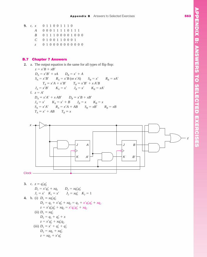
9. c. x 0 1 1 0 0 1 1 1 0A 0 0 0 1 1 1 1 0 1 1 1B 0 1 1 1 0 0 0 0 1 0 0 0C 0 1 0 0 1 1 0 0 0 1z 0 1 0 0 0 0 0 0 0 0 0 0
B.7 Chapter 7 Answers2. a. The output equation is the same for all types of flip flop:
z � x�B � xB�
DA � x�B� � xA DB � x� � ASA � x�B� RA � x�B (or x�A) SB � x� RB � xA�
TA � x�A � x�B� TB � x�B� � x A�BJA � x�B� KA � x� JB � x� KB � xA�
f. z � A�
DA � x�A� � x AB� DB � x�B � xB�
JA � x� KA � x� � B JB � x KB � xSA � x�A� RA � x�A � AB SB � xB� RB � xBTA � x� � AB TB � x
J B
B�K
J A
A�K
x
Clock
z
3. c. z � q1�q2�
D1 � x�q1� � xq1 D2 � xq1�q2�
J1 � x� K1 � x� J2 � xq1� K2 � 14. b. (i) D1 � xq1�q2�
D2 � q1 � x�q2� � xq2 � q1 � x�q1�q2� � xq2
z � x�q1�q2� � xq2 � x�q1�q2� � xq2
(ii) D1 � xq2�
D2 � q1 � q2� � x z � x�q2� � xq1�q2
(iii) D1 � x� � q1� � q2�
D2 � xq1 � xq2�
z � xq2 � x�q1�
AP
PE
ND
IX B
: AN
SW
ER
S T
O S
ELE
CT
ED
EX
ER
CIS
ES
Append ix B Answers to Selected Exercises 563
mar91647_apbb_556_572.qxd 12/2/08 11:30 AM Page 563

564 Append ix B Answers to Selected Exercises
0
2
3
6 7
4JK
D2
5
1
Brown path from 0 and 5 when DC � BA � B�A�
7. a. DD � CBA � DB� � DA� JD � CBA KD � BADC � D�C�BA � CB� � CA� JC � D�BA KC � BADB � B�A � BA� JB � KB � ADA � A� JA � KA � 1
8. b. DC � BA � {CB� or B�A�} JC � B KC � BA�
DB � B� � CA JB � 1 KB � C� � A�
DA � B� � A� JA � 1 KA � B
10. a. JA � B KA � x � B JB � x� � A� KB � 1b. 11 → 00
16. b.
C1
1
B0
E0
D0
1
A1
0
0
1
1
1
0
00
B E
D
A
C
0/0
1/0
1/00/0
0/0
1/0
1/0
0/11/0
0/0
f.
AP
PE
ND
IX B
: A
NS
WE
RS
TO
SE
LE
CT
ED
EX
ER
CIS
ES
mar91647_apbb_556_572.qxd 12/2/08 11:30 AM Page 564

1/0
C
A
1/0
E
1/0
0/0
0/0
0/0
0/0
0/0
0/0
0/0
0/1
G
1/0
D
B
1/0
1/0
1/1
F
1/0
H
A01
1
00
1
10
11
0
0
0
C0
D1
B0
E1
F1
k. l.
B.8 Chapter 8 Answers4. a. Assume CLR� is clocked, but does not require counter to be enabled.
z
x
D
EN
Clock
CLR�
C B A
b. z � x q1� q2� q3� q4� q5� q6� q7� q8
� x(q1 � q2 � q3 � q4 � q5 � q6 � q7)�q8
AP
PE
ND
IX B
: AN
SW
ER
S T
O S
ELE
CT
ED
EX
ER
CIS
ES
Append ix B Answers to Selected Exercises 565
mar91647_apbb_556_572.qxd 12/2/08 11:30 AM Page 565
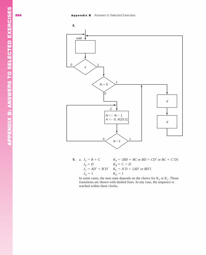
566 Append ix B Answers to Selected Exercises
s0
wait
1
1
1
0
0
N � 0
N �1
d
C
N �� N � 1A �� 0, A[15:1]
d
9. a. JA � B � C KA � {BD � BC or BD � CD� or BC � C�D}JB � D KB � C � DJC � AD� � B�D� KC � A�D � {AD� or BD�}JD � 1 KD � 1
In some cases, the next state depends on the choice for KA or KC. Thosetransitions are shown with dashed lines. In any case, the sequence isreached within three clocks.
8.
AP
PE
ND
IX B
: A
NS
WE
RS
TO
SE
LE
CT
ED
EX
ER
CIS
ES
mar91647_apbb_556_572.qxd 12/2/08 11:30 AM Page 566

11017
00000
1010
0110
1000 0101
0111
01004
00011
11108
10115
00113
11006
11119
00102
1001
X1 X2 X3 X4 X5 X6 X7
A�B�D� X X XB�CD X X X XABC X X XABD X X XA�C�D� X X XA�B�C� X XA�B�C X XABD� X X X XACD XBC�D� X
or inputs 4 5 5 3 2 3 4
b. A table for the minimal sum of product expressions is shown.
12. The state table for this counter follows:a. i. For the D flip flop, we have
DA � A�BC � x AB� � xAC�
DB � B�C � BC� � xA�B� � {AB or AC}DC � x�AC � xA�B� � xAC� � BC� � A�C�
The NAND gate requirements are
Size Number Packages
1 1 (x�) 0 (from 4)2 4 13 6 24 1 15� 1 1
AP
PE
ND
IX B
: AN
SW
ER
S T
O S
ELE
CT
ED
EX
ER
CIS
ES
The cost is thus $1.25 for gates plus the flip flops.
Append ix B Answers to Selected Exercises 567
mar91647_apbb_556_572.qxd 12/2/08 11:30 AM Page 567

568 Append ix B Answers to Selected Exercises
ii. Using JK flip flops, we get
JA � BC KA � x� � BCJB � C � xA� KB � A�CJC � x � A� � B KC � x�A� � xA � {xB or A�B}
For this, the NAND gate requirements are
The two extra NOT gates (1-input) are needed to create the ANDfor JA and KB. The cost is thus $1.00 for gates plus $2.00 for theflip flops, a total of $3.00.
b. Thus, if the D flip flop packages cost less than $0.875, the first solutionis less expensive.
If we can use one D package and one JK package, the best optionis to use the JK package for B and C, and one of the Ds for A (using xBand a shared xAB� in place of xA in KC). That would require
Size Number Packages
1 3 12 8 23 2 1
This solution would cost $2.00 plus the cost of the D package. If the Dpackage cost between $0.75 and $0.875, this solution would be better.
c. This flip flop will be set when the system is in state 5, 6, or 7 and x is0, or when in state 0 or 1 and the input is 1. It can be cleared wheneverthe system is in state 3. Thus, for the new flip flop,
J � xA�B� � x�AB � x�ACK � A�BC
and the output is just the state of that flip flop.d. All of the outputs come from flip flops. We can compute the inputs for
a D flip flop for Q using
D � Q� � JQ� � K�Q
Size Number Packages
1 2 0 (from 2’s)2 5 23 6 2
and then simplifying the algebra. The result is
D � AQ � B�Q � C�Q � xA�B� � x�AB � x�AC
AP
PE
ND
IX B
: A
NS
WE
RS
TO
SE
LE
CT
ED
EX
ER
CIS
ES
mar91647_apbb_556_572.qxd 12/2/08 11:30 AM Page 568

B�
B
D
x
Q C B A
C�
C
D
Q�
Q
D
Clock
A�
A
D
AP
PE
ND
IX B
: AN
SW
ER
S T
O S
ELE
CT
ED
EX
ER
CIS
ES
Append ix B Answers to Selected Exercises 569
mar91647_apbb_556_572.qxd 12/2/08 11:30 AM Page 569

570 Append ix B Answers to Selected Exercises
B.9 Chapter 9 Answers1. c.
q�
q x � 0 x � 1 z
A C A 0C C A 1
q� zq x � 0 x� 1 x � 0 x � 1
A B D 0 0B A B 1 0C B A 0 0D A C 1 1
k. The system cannot be reduced.
2. c. P1 � (AB)(CD)(E)P2 � (ABE)(CD)P3 � (A)(BC)(DE)P4 � (AB)(CDE)P5 � (A)(B)(C)(DE)
h. P1 � (AE)(B)(C)(D)(F)(G)P2 � (AEF)(BG)(C)(D)P3 � (AE)(BG)(C)(D)(F)
k. P1 � (ADG)(B)(C)(E)(F)P2 � (AE)(BCD)(FG)P3 � (AEFG)(BCD)P4 � (AG)(B)(C)(D)(E)(F)P5 � (A)(BC)(D)(E)(F)(G)P6 � (AE)(BCDFG)P7 � (A)(B)(C)(DG)(E)(F)P8 � (A)(B)(C)(D)(EF)(G)P9 � (ADG)(BC)(E)(F)P10 � (ADG)(B)(C)(EF)P11 � (AG)(BC)(D)(E)(F)P12 � (AG)(B)(C)(D)(EF)P13 � (A)(BC)(DG)(E)(F)P14 � (A)(BC)(D)(EF)(G)P15 � (A)(B)(C)(DG)(EF)P16 � (ADG)(BC)(EF)P17 � (AG)(BC)(D)(EF)P18 � (A)(BC)(DG)(EF)
h.
AP
PE
ND
IX B
: A
NS
WE
RS
TO
SE
LE
CT
ED
EX
ER
CIS
ES
mar91647_apbb_556_572.qxd 12/2/08 11:30 AM Page 570
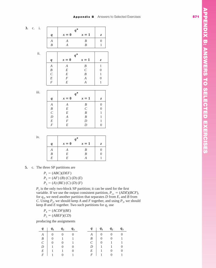
q�
q x � 0 x � 1 z
A A B 1B E C 0C E B 1E F A 0F E A 1
q�
q x � 0 x � 1 z
A A B 0B E C 0C E B 1D A B 1E F D 1F E D 0
q�
q x � 0 x � 1 z
A A B 0B E B 0E E A 1
q�
q x � 0 x � 1 z
A A B 0B A B 1
3. c. i.
ii.
iii.
iv.
5. c. The three SP partitions are
P1 � (ABC)(DEF )P2 � (AF ) (B) (C) (D) (E)P3 � (A) (BE) (C) (D) (F)
P1 is the only two-block SP partition; it can be used for the firstvariable. If we use the output consistent partition, POC � (ADE)(BCF),for q3, we need another partition that separates D from E, and B fromC. Using P2, we should keep A and F together, and using P3, we shouldkeep B and E together. Two such partitions for q2 use
P4 � (ACDF)(BE)P5 � (ABEF)(CD)
producing the assignments
q q1 q2 q3
A 0 0 0B 0 1 1C 0 0 1D 1 0 0E 1 1 0F 1 0 1
q q1 q2 q3
A 0 0 0B 0 0 1C 0 1 1D 1 1 0E 1 0 0F 1 0 1
AP
PE
ND
IX B
: AN
SW
ER
S T
O S
ELE
CT
ED
EX
ER
CIS
ES
Append ix B Answers to Selected Exercises 571
mar91647_apbb_556_572.qxd 12/2/08 11:30 AM Page 571

For the first assignment, the equations are
J1 � x� K1 � 1J2 � xq1q3 � xq1�q3� K2 � xJ3 � x� � q1� � q2 K3 � x�
z � q3�
using four gates with 11 inputs (plus a NOT).For the second assignment, the equations are
J1 � x� K1 � 1J2 � xq1q3� � xq1�q3 K2 � xq1
J3 � x� � q2� K3 � x�
z � q3�
using five gates with 12 inputs (plus a NOT).Using the first six binary numbers, the solution requires 11 gates
with 24 inputs (plus a NOT).
J1 � x�q2� K1 � 1J2 � xq1q3� � xq1�q3 K2 � xq3
J3 � x� � q1�q2� K3 � x� � q1�
z � q2�q�3 � q2q3
572 Append ix B Answers to Selected Exercises
AP
PE
ND
IX B
: A
NS
WE
RS
TO
SE
LE
CT
ED
EX
ER
CIS
ES
mar91647_apbb_556_572.qxd 12/2/08 11:30 AM Page 572
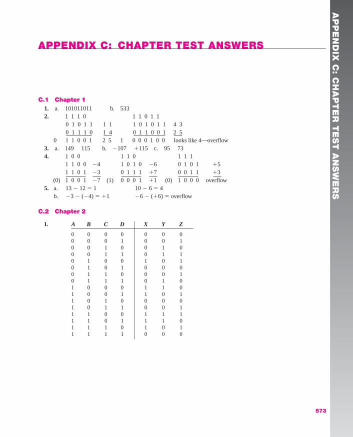
C.1 Chapter 11. a. 101011011 b. 5332. 1 1 1 0 1 1 0 1 1
0 1 0 1 1 1 1 1 0 1 0 1 1 4 30 1 1 1 0 1 4 0 1 1 0 0 1 2 5
0 1 1 0 0 1 2 5 1 0 0 0 1 0 0 looks like 4—overflow3. a. 149 115 b. �107 �115 c. 95 734. 1 0 0 1 1 0 1 1 1
1 1 0 0 �4 1 0 1 0 �6 0 1 0 1 �51 1 0 1 �3 0 1 1 1 �7 0 0 1 1 �3
(0) 1 0 0 1 �7 (1) 0 0 0 1 �1 (0) 1 0 0 0 overflow5. a. 13 � 12 � 1 10 � 6 � 4
b. �3 � (�4) � �1 �6 � (�6) � overflow
C.2 Chapter 2
A B C D X Y Z
0 0 0 0 0 0 00 0 0 1 0 0 10 0 1 0 0 1 00 0 1 1 0 1 10 1 0 0 1 0 10 1 0 1 0 0 00 1 1 0 0 0 10 1 1 1 0 1 01 0 0 0 1 1 01 0 0 1 1 0 11 0 1 0 0 0 01 0 1 1 0 0 11 1 0 0 1 1 11 1 0 1 1 1 01 1 1 0 1 0 11 1 1 1 0 0 0
1.
APPENDIX C: CHAPTER TEST ANSWERS
AP
PE
ND
IX C
: CH
AP
TE
R T
ES
T A
NS
WE
RS
573
mar91647_apc_573_586.qxd 12/2/08 10:02 AM Page 573

NOT equal3. a�c � ab�
574 Append ix C Chapter Test Answers
a b c f g
0 0 0 1 10 0 1 1 10 1 0 1 10 1 1 0 01 0 0 0 01 0 1 0 01 1 0 1 11 1 1 1 0
2.
a
d
b
f
b�c
a
d
4. a.
b.
b�
c
d
a
b
d
f
5. a. f (x, y, z) � �m(0, 2, 3, 5, 7)b. f � x�y�z� � x�yz� � x�yz � xy�z � xyzc. f � x�z� � x�y � xz � x�z� � xz � yzd. f � (x � y � z�) (x� � y � z) (x� � y� � z)e. f � (x � y � z�) (x� � z)
AP
PE
ND
IX C
: C
HA
PT
ER
TE
ST
AN
SW
ER
S
mar91647_apc_573_586.qxd 12/2/08 10:02 AM Page 574
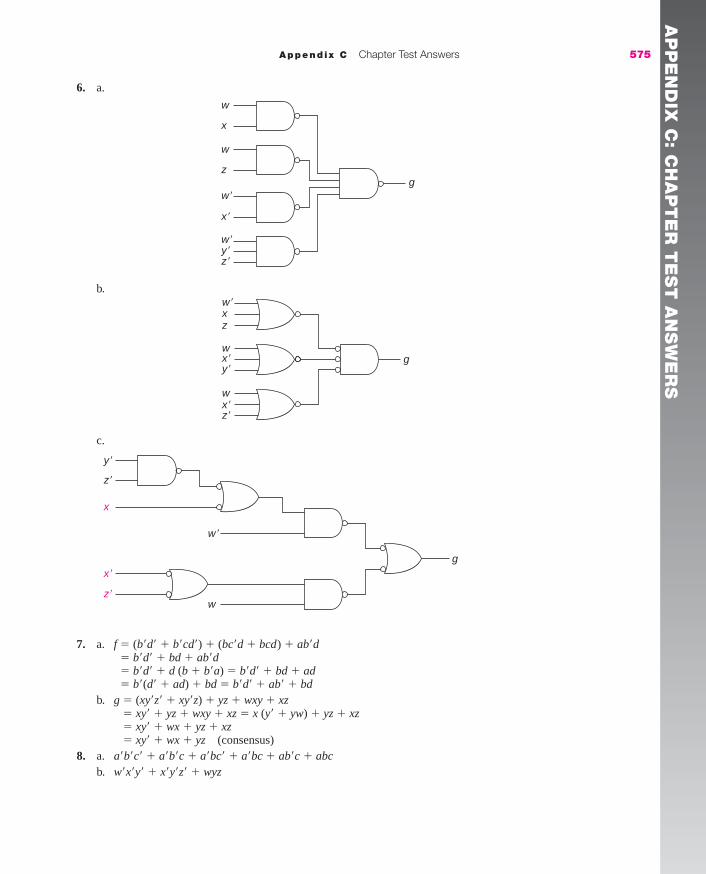
7. a. f � (b�d� � b�cd�) � (bc�d � bcd) � ab�d� b�d� � bd � ab�d� b�d� � d (b � b�a) � b�d� � bd � ad� b�(d� � ad) � bd � b�d� � ab� � bd
b. g � (xy�z� � xy�z) � yz � wxy � xz� xy� � yz � wxy � xz � x (y� � yw) � yz � xz� xy� � wx � yz � xz� xy� � wx � yz (consensus)
8. a. a�b�c� � a�b�c � a�bc� � a�bc � ab�c � abcb. w�x�y� � x�y�z� � wyz
Append ix C Chapter Test Answers 575
6. a.
b.
c.
w�xz
wx�y�
wx�z�
g
w
x
w�
g
y�
z�
x�
z�
w
x
g
w�
w�
y�z�
w
z
x�
AP
PE
ND
IX C
: CH
AP
TE
R T
ES
T A
NS
WE
RS
mar91647_apc_573_586.qxd 12/2/08 10:02 AM Page 575

C.3 Chapter 31. a. f (x, y, z) � �m (1, 2, 7) � �d(4, 5)
b. g � a�c � ab�c�d � a�bd � abc�
576 Append ix C Chapter Test Answers
9.
10.
f
c
d
b
a�
d�
b�
a
c
g
c
a�
a
d�
e
d�
e�
c
b�
c�
00 01 11 10
0
1
x y
z
X
X
1
1 1
00 01 11 10
00
01
11
10
a b
c d
1
1 1
1
1
11 1
AP
PE
ND
IX C
: C
HA
PT
ER
TE
ST
AN
SW
ER
S
mar91647_apc_573_586.qxd 12/2/08 10:02 AM Page 576

2. a. wx�y�z� � wyz � w�x b. acd � a�c� � a�d� � ab3. b�d � bd� � ac � {ab or ad} � {a�b�c� or a�c�d�}4. wz� � {x�z or wx�} � {xy�z� or w�xy�}5. f � a�d � {c�d or b�d}
f � d(a� � b�) � d(a� � c�)6. f � wx � {xy�z or w�y�z} � {wyz or x�yz}
f � (w � z)(x � y){(x � z) or (y� � z)}{(x� � y�) or (w � y�)}7. A�B�C� � ACE � ABC�D � BCD�E� � {A�B�D�E or B�CD�E}8. ACE� � CDE � A�C�E� � BC�E � AB�C�
ACE� � CDE � B�C�E� � A�BC� � AC�E9. a. f � xy�z� � wx� � wz�
g � w�z � w�xy � x�zb. f � xy�z� � wz� � wx�z
g � w�z � w�xy � wx�z10. a. f � w�z � w�y � yz � wx�z�
g � w�yz� � xz� � wxy � wy�z�
h � w�z � w�x � xyz � wx�y�z�
b. f � w�z � w�yz� � wx�y�z� � wxyz � x�yg � w�yz� � xz� � wx�y�z� � wxyzh � w�z � wx�y�z� � wxyz � w�x
Append ix C Chapter Test Answers 577
C.4 Chapter 41. w�x�, x�y�z�, w�yz�, w�y�z, wy�z�, wxyz
2. g � a�cd � bd� � ac� � {a�b or bc�}
3. terms for both: x�yz�, w�xz, wx�yf : w�y�z, wyz, xzg: w�xy�, w�yz, x�z�, y�z�, x�y
4. f � a�d� � a�cdg � b�d� � bd � a�cd
AP
PE
ND
IX C
: CH
AP
TE
R T
ES
T A
NS
WE
RS
mar91647_apc_573_586.qxd 12/2/08 10:02 AM Page 577

578 Append ix C Chapter Test Answers
f
x
y
z
ab
c
w
0
1
2
3
4
5
6
7EN2 �
EN11
x
y
z
ab
c
0
0
1
2
3
4
5
6
7EN2 �
EN1w
g
2.
w x y z
f
w�z
w�yz�
wx�y�z�
wxyz
x�y
xz�
w�x
hg
C.5 Chapter 51.
AP
PE
ND
IX C
: C
HA
PT
ER
TE
ST
AN
SW
ER
S
mar91647_apc_573_586.qxd 12/2/08 10:02 AM Page 578

Append ix C Chapter Test Answers 579
3.
w x y z
f
0
1
2
3
4
5
6
7
8
9
10
11
12
13
14
15
hg
AP
PE
ND
IX C
: CH
AP
TE
R T
ES
T A
NS
WE
RS
mar91647_apc_573_586.qxd 12/2/08 10:02 AM Page 579

580 Append ix C Chapter Test Answers
4.
w
w�z
w�y
wx�z�
w�yz�
xz�
wy �z �
w �z
w�x
wx�y �z �
xyz
wxy
yz
x y z
f
g
h
AP
PE
ND
IX C
: C
HA
PT
ER
TE
ST
AN
SW
ER
S
mar91647_apc_573_586.qxd 12/2/08 10:02 AM Page 580

Append ix C Chapter Test Answers 581
5.
0
1
2
3
0
2
4
6b
ax
y
EN�
0
1
2
3
0
b
aw
z
EN�
0
1
2
3
8
10
12
14b
a
EN�
0
1
2
3
9
11
13
15b
a
EN�
f
h
g
C.6 Chapter 6
1. x 0 0 1 1 0 0 0 1 0 1q A C B D B A C B D B D Bz 0 0 1 0 1 0 0 1 0 1 0 1 0
AP
PE
ND
IX C
: CH
AP
TE
R T
ES
T A
NS
WE
RS
mar91647_apc_573_586.qxd 12/2/08 10:02 AM Page 581

582 Append ix C Chapter Test Answers
Clock
K
Q
Q
J
CLR
a.
b.
3. D � xB � x�B� T � A� � x z � A� � B
4. DA � xB� � x�B DB � x � A� z � AB
2.
A�B� zAB x � 0 x � 1 x � 1
0 0 1 1 0 1 10 1 0 0 1 0 11 0 1 0 0 1 01 1 0 1 1 0 1
Clock
A
B
x
z
AP
PE
ND
IX C
: C
HA
PT
ER
TE
ST
AN
SW
ER
S
mar91647_apc_573_586.qxd 12/2/08 10:02 AM Page 582

Append ix C Chapter Test Answers 583
C.7 Chapter 71. DA � x�B� � xB JB � KB � A� � x z � x�A � xB�
2. S1 � x R1 � x�q2 J2 � xq1 K2 � x� z � q2�
3. a. D1 � x�q1� � x�q2 � q1�q2 � xq1q2�
D2 � x � q1�q2 z � q1�q2�
b. D1 � x � q1q2 D2 � q2� z � q1�q2�
c.
q2
q2�
D
z
q1
q1�
Dx
Clock
4. D � A� J � C� K � A�C� T � A� � B�C�
7 30
6
4
5
2
1
5. a. b.
1/0
0/1
0/0
1/0
0/0
1/0
1/0
0/0
A
CB
D
1/0
0/0
1/0
0/0
1/0
0/1
1/0
0/0
A
CB
D
AP
PE
ND
IX C
: CH
AP
TE
R T
ES
T A
NS
WE
RS
mar91647_apc_573_586.qxd 12/2/08 10:02 AM Page 583
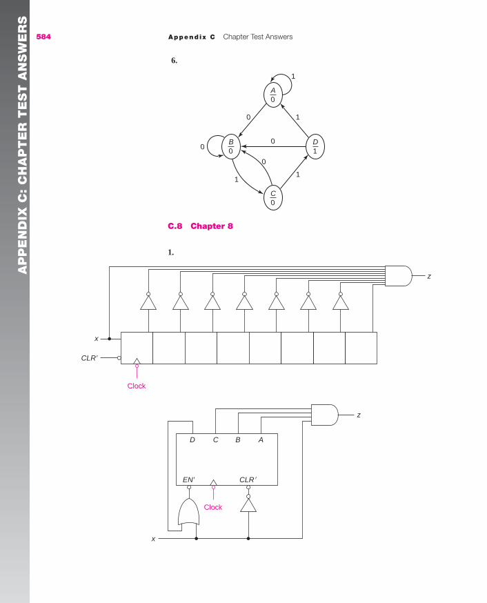
584 Append ix C Chapter Test Answers
6.
C.8 Chapter 8
0
1
0
1
10
0
C0
D1
A0
B0
1
D
x
C B A
z
EN� CLR�
Clock
x
CLR�
Clock
z
1.
AP
PE
ND
IX C
: C
HA
PT
ER
TE
ST
AN
SW
ER
S
mar91647_apc_573_586.qxd 12/2/08 10:02 AM Page 584

Append ix C Chapter Test Answers 585
2.
0 1
00
01
11
10
x
DA DB
DA
A B
1
1
1
1
0 1
00
01
11
10
x
A B
1
1
1
1
1
1
= x �A� + x A DB= x + B �
z
0 1
00
01
11
10
x
A B
1
1
1
1
z = x �B� + x A
Clock
D
Q �
Q
D
Q �
Q
x
B A
A�
B �
z
AP
PE
ND
IX C
: CH
AP
TE
R T
ES
T A
NS
WE
RS
mar91647_apc_573_586.qxd 12/2/08 10:02 AM Page 585

586 Append ix C Chapter Test Answers
C.9 Chapter 91.
2. a. P1 � output consistentP2 � SPP3 � neitherP4 � SP, output consistentP5 � SPP6 � SP, output consistent
b. P4 allows us to reduce the system to that of Problem 1.3. P1 � (AC)(B)(D)
P2 � (AD)(BC)P3 � (A)(BD)(C)P4 � (AC)(BD)
4. Use P3 for q1 and POC � (ACE) (BDF) for q2. The product of these is (AE)(BD) (C) (E). Using P2, we keep A and F together, and B and C together.That gives either (ADF) (BCE) or (ABCF) (DE) as good partitions for q3.Using the latter, we get
D1 � x � q1�
D2 � x�q1�q3� � xq1 � q1q2q3� � xq2�
D3 � x�q1�q3� � xq1 � {q1q3 or q2q3}z � q2�
q�
q x � 0 x � 1 z
A-B C-D A-B 0C-D E A-B 0E C-D A-B 1
AP
PE
ND
IX C
: C
HA
PT
ER
TE
ST
AN
SW
ER
S
mar91647_apc_573_586.qxd 12/2/08 10:02 AM Page 586

587
In the following sections, we will introduce three tools for imple-menting or simulating the circuits designed in the text. There willthen be a variety of experiments, keyed to the material in the body of
the text.First, in D.1, we will describe a setup where integrated circuit pack-
ages will be wired and tested.Second, in D.2, we will introduce a breadboard simulator that allows
us to do the hardware experiments without requiring the laboratoryequipment. The wiring of Section D.1 is done on a PC screen.
Next, in D.3, we will introduce LogicWorks, so that the behavior ofcircuits can be simulated, without actually building them. This will beparticularly valuable to observe the timing behavior of the circuit, with-out the use of a logic analyzer.
We will then, in D.4, provide a set of experiments that can beaccomplished with each of these systems.
The pin layout of all the integrated circuits referenced in the text isshown in D.5. Note that different manufacturers use different notations.We will follow the notation in the text.
D.1 HARDWARE LOGIC LAB
Logic circuits can be built and tested using a small breadboard that allowsthe user to plug in integrated circuit chips and wires (without making per-manent solder connections). The additional equipment needed to per-form most of these experiments are a 5-volt power supply (or battery),some switches, some LEDs (lights to display binary values), and a squarewave generator with a 5-volt output (with variable speed capabilities).Some of the later experiments also use a pair of seven-segment displaysand a pulser. The IDL-800 Logic Lab* provides a convenient way to buildand test small and medium size digital circuits and includes all of the fea-tures described above and many others.
Circuits are wired on the breadboard, a small portion of which isshown in Figure D.1. (The breadboard in the next section [Figure D.6] isa computer simulation of this.) The main part of the breadboard has a
APPENDIX D: LABORATORY EXPERIMENTS
*Manufactured by K & H Mfg. Co., Ltd.
AP
PE
ND
IX D
: LA
BO
RA
TO
RY
EX
PE
RIM
EN
TS
mar91647_apd_587_611.qxd 12/2/08 5:02 PM Page 587

number of grooves, over which an integrated circuit chip fits, as indi-cated in Figure D.1. The chip fits in the first of a set of six holes, each ofwhich is connected together internally. Thus, to connect something to apin, the wire is inserted in one of those holes. (Do not put another chipover the groove next to the first one; the pins of the two chips would beconnected. Immediately above and below the main section on manyboards, there are two busses. One is usually used for ground. The other isusually used for �5 volts. On some boards, the various sections of thebus are connected internally; on others, they must be wired together.Some boards also have, on the bottom of the board, a set of pins incolumns that are internally connected and used mostly for external sig-nals that are to be connected to several places.
the semicircle) to 7 down the left side and then from 8 to 14 up the rightside. (If there are more pins, the numbering is the same, starting at theupper left and continuing down the left side and up the right side.)
588 Append ix D Laboratory Experiments
Figure D.1 Detail of the breadboard.
IC pin insertedin hole
Integrated circuit Set of six holes forwire insertion — allinterconnected internally
Connections tothat pin maybe made in anyof these Groove
The integrated circuit package illustrated has 14 pins (as do all ofthem in the experiments in Chapter 2). The orientation of the chip is spec-ified by the semicircle (at the top). Typically, that is just an indentation inthe plastic shell of the chip. Pins are numbered from 1 (at the top, left of
AP
PE
ND
IX D
: LA
BO
RA
TO
RY
EX
PE
RIM
EN
TS
mar91647_apd_587_611.qxd 12/2/08 5:02 PM Page 588

D.1 Hardware Logic Lab 589
Figure D.2 Layout of the 7400.
1
2
3
4
5
6
GND
Vcc � 5 V
13
12
11
10
9
8
1
23
0 0
6
8
11
4
5
9
10
12
13
The first highlights the orientation of the pin connections; the secondemphasizes the individual gates. From a wiring point of view, we aredealing with the first on the circuit board.
To illustrate the use of the system, consider the implementation ofthe function
f � ab� � bc
using NAND gates. The circuit for this is shown in Figure D.3.
Figure D.3 A NAND gate circuit.
f
a
b
c
Since complemented inputs are often not available, b� was created usinga NAND gate. (We could have done this with a NOT gate, but the 7400has four NAND gates, and we can use the extra one as a NOT.)
In order to wire this, we need to associate each gate with one on thechip and find the pin numbers. The circuit is redrawn in Figure D.4 withthe pin numbers indicated.
A closer look at the 7400 (with 4 two-input NAND gates) is shownin Figure D.2 in two formats:
AP
PE
ND
IX D
: LA
BO
RA
TO
RY
EX
PE
RIM
EN
TS
mar91647_apd_587_611.qxd 12/2/08 5:02 PM Page 589

Now the connections can be made on the breadboard. The circuit ofFigure D.5 shows the appropriate connections for this system. Note thatit does not matter which of the five holes are used to connect somethingto a chip’s pin. However, only one wire can fit in a hole; thus, when thesame signal goes to several points, more than one of the holes is used (orone of the set of holes at the bottom of the board is used). Thus, forexample, input b goes to pins 4, 5, and 13. In Figure D.5, it is connecteddirectly to pin 4; then a wire is run from pin 4 to pin 5 and from pin 4 topin 13. (It could have gone from pin 5 to 13.)
590 Append ix D Laboratory Experiments
Figure D.4 NAND circuit with pins
f
a
b
c
13
2
108
9
1112
134 5
6
Figure D.5 Wiring for 7400 circuit.
SWITCHA
Gnd
SWITCHB
SWITCHC
LIGHTF
�5
1
2
3
4
5
6
7
14
13
12
11
10
9
8
After the breadboard is wired (and before the power is turned on),connect the breadboard to the voltages, input switches, and output lights.The power can then be turned on and the system tested. (Caution: Do notinsert or remove wires while the power is on.)
As an introduction to the system, build this circuit and test it. To testit, start with the three switches all in the 0 position and observe the out-put light. Repeat for each of the eight input combinations. Compare thatwith the truth table that was constructed based on the algebra.
AP
PE
ND
IX D
: LA
BO
RA
TO
RY
EX
PE
RIM
EN
TS
mar91647_apd_587_611.qxd 12/2/08 5:02 PM Page 590

D.2 WinBreadboard™ and MacBreadboard™ 591
Seven-segment displays are useful to output decimal results. Adigit (in 8421 code) is input to a decoder/driver, the outputs of whichprovide the signals to light the display. The IDL-800 logic lab has two seven-segment displays. The BCD inputs to the decoder allow the con-nection of a BCD number (8421 code) to be displayed on either of thedisplays. Below each display, there is an active low enable input for thatdisplay. To use both displays, the inputs must be alternated. (The dis-plays will look like they are lit even if the inputs are there only half of thetime, as long as they alternate at a rate of about 60 Hz or higher.) If anycode that does not correspond to a decimal digit (1010 and above) isentered, the display will remain blank. (There is also a P input that lightsa decimal point on the right of the display.)
D.2 WINBREADBOARD™ ANDMACBREADBOARD™*
The MacBreadboard, shown in Figure D.6, (also available for Windowsas WinBreadboard) is a computer simulation of the logic laboratorydescribed in Section D.1. A picture of the screen before building a circuitis shown in Figure D.6.
*Product of Yoeric Software, Chapel Hill, NC. The software can be purchased at http://www.yoeric.com/breadboard.htm.
Figure D.6 Breadboard.
AP
PE
ND
IX D
: LA
BO
RA
TO
RY
EX
PE
RIM
EN
TS
mar91647_apd_587_611.qxd 12/2/08 5:02 PM Page 591

This looks very similar to the hardware laboratory and has many ofthe same features. (Anyone who is not familiar with the hardware labo-ratory should review Section D.1 before proceeding). The pull-downmenu “chips” provides a selection of more than 70 chips from the 7400series. When a chip is selected, it is automatically placed* on the left endof the board. However, it can be moved to any position by clicking onand dragging it. When the chip is double clicked, the pin layout of thatchip is displayed.
The top row of holes (labeled X) are connected together; they areusually connected to �5. Similarly, the bottom row (labeled Y) are con-nected and are used for ground. A wire connection must be madebetween one of the holes in these rows and �5 and ground. To connect awire, click on a hole and drag to the other hole to which it is to be con-nected. Wires only run horizontally or vertically (not diagonally). If thepointer does not follow a straight line, the wire may zig zag across theboard. To prevent this, hold down the shift key; the wire will then followa straight line. On a color display, the wires can be made one of severalcolors. Either select the color before drawing the wire or click once onthe wire and then select a color from the “color” pull-down list.
There are a set of four input switches (with uncomplemented andcomplemented outputs), labeled D, C, B, and A. There is also another setof eight switches (L to E) with only uncomplemented outputs. There is aset of four output LEDs (4 to 1). An active high signal can be connectedto the � side and the other side to ground or an active low signal to the� side and the � side to 5 volts. There is also a set of 10 logic indicators(which are just active high output lights). The four switches and fourLEDs can be labeled; those names will appear in the timing diagram.
A circuit with one NAND gate from a 7400 connected (with theinputs and outputs labeled) and a 7410 place on the board, but not con-nected is shown in Figure D.7.† If the system is turned on in this position,LED4 will be lit.
The breadboard has two seven-segment displays, each with a set offour inputs. It displays hexadecimal. (Of course, if the inputs are limitedto the ten digits, the display is limited to 0 to 9, BCD in 8421 code.)
Some of the experiments, particularly in Chapters 6, 7, and 8, makeuse of the clock and pulser. The clock produces a square wave, the fre-quency of which can be controlled by the slide. (It has very low frequen-cies, from about 0.15 to 10 Hz; but that is all one can view.) The “clock”pull-down menu provides for pulses or steps, so that it is possible tofollow the behavior of the system one clock pulse at a time. A timingdiagram can be displayed (from the clock menu). The clock and alllabeled switches and output LEDs will be displayed. The breadboard cir-
592 Append ix D Laboratory Experiments
*The on/off switch must be in the off position to make any connections on the circuitboard. Click on the switch to change it.
†As the diagrams get more complex, it is particularly important to draw the wires neatlyand to use colors to signify meaning. For example, black is commonly used for groundand red for �5. (Colors are not obvious in this black and white picture.)
AP
PE
ND
IX D
: LA
BO
RA
TO
RY
EX
PE
RIM
EN
TS
mar91647_apd_587_611.qxd 12/2/08 5:02 PM Page 592
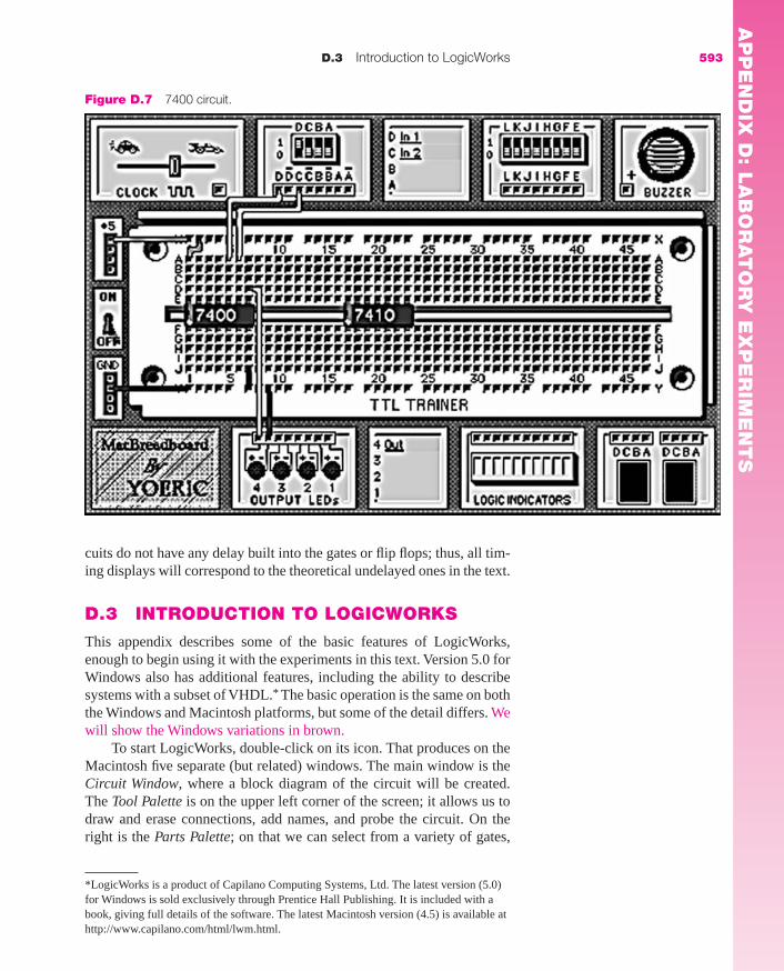
D.3 Introduction to LogicWorks 593
cuits do not have any delay built into the gates or flip flops; thus, all tim-ing displays will correspond to the theoretical undelayed ones in the text.
D.3 INTRODUCTION TO LOGICWORKS
This appendix describes some of the basic features of LogicWorks,enough to begin using it with the experiments in this text. Version 5.0 forWindows also has additional features, including the ability to describesystems with a subset of VHDL.* The basic operation is the same on boththe Windows and Macintosh platforms, but some of the detail differs. Wewill show the Windows variations in brown.
To start LogicWorks, double-click on its icon. That produces on theMacintosh five separate (but related) windows. The main window is theCircuit Window, where a block diagram of the circuit will be created.The Tool Palette is on the upper left corner of the screen; it allows us todraw and erase connections, add names, and probe the circuit. On theright is the Parts Palette; on that we can select from a variety of gates,
Figure D.7 7400 circuit.
*LogicWorks is a product of Capilano Computing Systems, Ltd. The latest version (5.0)for Windows is sold exclusively through Prentice Hall Publishing. It is included with abook, giving full details of the software. The latest Macintosh version (4.5) is available athttp://www.capilano.com/html/lwm.html.
AP
PE
ND
IX D
: LA
BO
RA
TO
RY
EX
PE
RIM
EN
TS
mar91647_apd_587_611.qxd 12/2/08 5:02 PM Page 593

integrated circuits, inputs, and displays. The bottom of the screen is theTiming Window, where a trace of the behavior of the circuit over time isdisplayed. Finally, in the upper left corner of that, is the SimulatorPalette, that gives control of various features of the timing trace. InWindows, the Tool Palette and the Simulator Palette are replaced by asingle Tool Bar (with basically the same functionality). We will use theword palette in the discussion below for both platforms.
We will first build and test a simple combinational logic circuit toimplement
f � ab� � bc.
The block diagram of the circuit as we will construct it is shown inFigure D.8.
594 Append ix D Laboratory Experiments
Figure D.8 LogicWorks example.
a
b
c
f
To build a model of this circuit with LogicWorks, first go to the partspalette, then click and drag the mouse on the title to highlight SimulationGates.clf. A list of the types of gates that are available will appear. (Win-dows: All parts are merged into a single list; we will refer to Macintoshindividual palettes in the text below.) For this problem, double-click onAND-2. When the cursor moves over the circuit window, a picture of thegate will appear. Move it to the center of the window and click. At thatpoint, the gate will be fixed on the screen and another copy will appear.Since a second AND gate is needed, move it to a convenient spot andclick again. When that type of gate is no longer needed, hit the space bar(or click on the arrow on the Tool Palette). Return to the Parts Palette,move down to the OR-2, and repeat the process. The final component isa NOT gate, obtained in the same way, except that we want it pointingup. To accomplish that, push the up arrow (↑) key while the gate isselected and then click it into position. Any gate may be highlighted byclicking on it, and then moved by dragging the mouse. (The orientationof a gate may be changed when it is highlighted by pulling down the leftbox on the Tool Palette and selecting the desired direction. (The sidebubble is relevant only in three-state gates; it may be ignored for now.)(This can be accomplished in Windows by selecting the Orientationmenu from the Schematic pull-down menu.) The screen should now looksomething like Figure D.9.
AP
PE
ND
IX D
: LA
BO
RA
TO
RY
EX
PE
RIM
EN
TS
mar91647_apd_587_611.qxd 12/2/08 5:03 PM Page 594

Now that all the gates are on the diagram, they need to be connected.Point to the end of any line and drag it to where it is to be connected.The path may be varied by depressing the key and/or the option key(CTRL and/or TAB key). If none of those paths are satisfactory, draw aline and release the mouse; then start again in another direction. Finally,a line can be drawn anywhere by clicking on the � cursor on the toolpalette and dragging the mouse where the line is to go. At the end of theline click once to start a new line or double click to terminate line draw-ing. To remove a line (or a gate), select the Zap (lightning bolt) tool in theTool Palette and point it to what is to be deleted. An alternative is to high-light the item and use the delete key. To get out of the zap mode, hit thespace bar or the arrow on the Tool Palette.
Next, names can be added to the inputs and outputs (or any point inthe circuit). To do this, use the Text Tool (the A on the Tool Palette).When that is highlighted, a pencil point is displayed. Move the point tothe line that is to be named and click the mouse. An internal name will bedisplayed; just type over that. Move the name to wherever it is most con-venient by clicking at the point to be named and then dragging to wherethe name is to be written. To exit text mode, use the arrow on the ToolPalette (or select some other tool); the space bar enters a space in the text.
To connect inputs, connect any point to ground or �5 volts, foundon the CONNECT.CLF parts menu or the DemoLib.clf parts menu.There is also a binary switch (found on the DemoLib.clf parts menu).Clicking on that switch causes its value to change between 0 and 1.Finally, the probe tool (shown on the Tool Palette with a ?) can be usedto test the value at any point. With that pointed and the mouse depressed,type in a 0 or 1 to set the value at that point. The probe will display a Zfor an input that is not connected to anything and an X for a point whosevalue is unknown (for example, the output of a gate, the inputs of whichare not specified). The output can be displayed permanently, using thebinary probe from the DemoLib.clf parts menu.
The circuit, as completed, using switches for inputs and the binaryprobe for outputs, is shown in Figure D.10, first with all of the switchesin the 0 position (producing a 0 output) and then with a in the 1 positionand b � c � 0 (producing a 1 output).
D.3 Introduction to LogicWorks 595
Figure D.9 Parts placed.
AP
PE
ND
IX D
: LA
BO
RA
TO
RY
EX
PE
RIM
EN
TS
mar91647_apd_587_611.qxd 12/2/08 5:03 PM Page 595

596 Append ix D Laboratory Experiments
With switches and the probe in place, it is easy to complete the truthtable for this function. As an introduction to LogicWorks, create this cir-cuit and test it.
By selecting the 7400DEVS.CLF menu from the Parts Palette, alogic diagram for that chip appears on the Circuit window. (A large vari-ety of 7400 series chips are available; we will reference many of them inthe experiments that follow.) It can be clicked in place, just as any of theother components. Connections can then be made as before. The circuitfor
f � ab� � bc
using 4 two-input NAND gates is shown in Figure D.11.
Figure D.10 Completed circuit with input switches and output display.
f
a
b
c
10
10
01
0
f
a
b
c
10
10
01
1
Figure D.11 Circuit using a 7400.
1
23
0 0
6
8
11
4
5
9
10
12
13
a
b
f
c
As before, it can be tested by connecting switches to the inputs or byconnecting each to ground or 5 volts. Try this and see that it also works.
Finally, we will look at one other method of connection. If twopoints are given the same name, they are treated as if they are connected(even though no connection line is drawn). Thus, in the circuit ofFigure D.12, all of the connections of the above diagram are made,switches are connected to each of the inputs, and a binary probe is con-nected to the output.
AP
PE
ND
IX D
: LA
BO
RA
TO
RY
EX
PE
RIM
EN
TS
mar91647_apd_587_611.qxd 12/2/08 5:03 PM Page 596

Parts of a circuit may be highlighted by clicking on them (in pointmode). Hold the shift key down to highlight several parts. Also, bydragging the mouse from outside one corner of a circuit to outside thediagonal corner, a box is created such that, when the mouse is released,everything within the box is selected. To select the whole drawing, pulldown Select All from the Edit menu. The Copy feature can be used totake this drawing and insert it in another document (perhaps a wordprocessor). A drawing can also be printed directly from LogicWorksfrom the File menu. (All of these also work to copy or print a timingdiagram when the Timing Window is highlighted.)
To examine some of the other ideas, we first need to look at the clockand the Timing Window. The clock is found on either the DemoLib.clf orSimulation IO.clf menu. It provides a square wave with a period of20 units, unless modified (as described below). Any signal that is namedwill be displayed in the Timing Window. The speed of the display is con-trolled on the Simulator Palette (by buttons on the bottom row of the ToolBar). By sliding the speed control bar to the left, the display can beslowed. At the left end, it stops. Click Step (symbol of man standing) tomove from one event to the next. (An event is any point where a signalmight change.) The display can be magnified by clicking on �� orshrunk by clicking on ��. The clock speed can be controlled by click-ing on the clock (to highlight it) and pulling down Simulation Params . . .from the Simulate (Simulation) pull-down menu. Set the time the clockis low and the clock is high; then exit the menu by hitting return.
Every combinational logic device has a built-in delay of 1 time unit.That can be seen by connecting the clock to a device and observing theinput and the output of that device. The delay can be changed usingSimulation Params . . . with that device highlighted. To see the behavior,set up the circuit of Figure D.13 and set the clock to 40 units for both lowand high. Set the delay to 10 units for each gate.
D.3 Introduction to LogicWorks 597
Figure D.12 Named connections.
t
t
fs
s
c
b
b
b
b�
b�
a
b10
f
1
a10
c10
1
23
0 0
6
8
11
4
5
9
10
12
13
AP
PE
ND
IX D
: LA
BO
RA
TO
RY
EX
PE
RIM
EN
TS
mar91647_apd_587_611.qxd 12/2/08 5:03 PM Page 597

598 Append ix D Laboratory Experiments
Figure D.13 Delay example.
c
b
a
� 5 V
Figure D.14 Timing diagram.
100
a
b
c
Stop the clock by moving the speed bar to the far left. Click on Restart ( ), which reinitializes the clock. Expand the display by clicking on��. Then click once or twice on the right arrow of the speed bar to startthe simulation. When it is stopped after 120 units, a display like the oneof Figure D.14 is seen. Note that c is a duplicate of a delayed by 20 units(after the startup).
D.4 A SET OF LOGIC DESIGNEXPERIMENTS
Each of the experiments can be implemented on any of the systems withthe modifications indicated. The notation below will be used to indicatethe special needs.
HW: Hardware Logic Lab
BB: Breadboard Simulator
LW: LogicWorks
D.4.1 Experiments Based on Chapter 2 Material
■ 1. For each of the following sets of functions, build each versionusing AND, OR, and NOT gates. Test them to show that eachfunction in a set behaves the same as each of the others inthat set.
a. f � xy�z� � xy�z � xyzg � xy� � xzh � x(y� � z)
b. f � a�b�c� � a�b�c � abc� � ab�c�g � a�b� � ac�h � (a� � c�)(a � b�)
AP
PE
ND
IX D
: LA
BO
RA
TO
RY
EX
PE
RIM
EN
TS
mar91647_apd_587_611.qxd 12/2/08 5:03 PM Page 598
D.4 A Set of Logic Design Experiments 599
c. f � x�yz� � xyz� � xy�zg � yz� � xz�h � z�(x � y�)
d. f � a�bc� � ab�c� � a�bc � ab�cg � (a � b)(a� � b�)h � a�b � ab�
e. f � x�y�z� � x�yz� � xyz � xy�zg � x�z� � xzh � (x� � z)(x � z�)
f. f � a�b�c � a�bc � abcg � a�c � bch � c(a� � b)
HW: Use one 7404 (NOT gates) to construct the complement ofthe variables. (Use the same 7404 outputs for all three versions.)
HW, BB: In addition, we have available 7411s (three-input ANDgates), 7408s (two-input AND gates), and 7432s (two-input ORgates). There are no larger OR gates available and thus we mustconstruct a multi-input OR gate from two-input gates. Each ofthe outputs should go to a different light, but the inputs comefrom the same three switches.
LW: Use individual gates (from Simulation Gates.clf).
■ 2. Implement the systems of Experiment 1 using NAND gates forthe sum of products expressions and NOR gates for the productof sums expressions.
HW, BB: Use 7400s, 7410s, 7430s, and 7402s (two-input NORgates).
LW: Use individual gates.
■ 3. Implement each of the following expressions (which are alreadyin minimum sum of products form) using only 7400s (two-inputNAND gates). No gate may be used as a NOT (except to form thecomplement of the inputs). Note that these are the functions ofExercise 25 in Chapter 2, where the number of two-input gates(not including the NOT gates) is shown in parentheses.
a. f � wy� � wxz� � y�z � w�x�z (7 gates)b. ab�d� � bde� � bc�d � a�ce (10 gates)c. H � A�B�E� � A�B�CD� � B�D�E� � BDE�
� BC�E � ACE� (14 gates)d. F � A�B�D� � ABC� � B�CD�E � A�B�C
� BC�D (11 gates)e. G � B�D�E� � A�BC�D � ACE � AC�E� � B�CE
(12 gates, one of which is shared)
AP
PE
ND
IX D
: LA
BO
RA
TO
RY
EX
PE
RIM
EN
TS
mar91647_apd_587_611.qxd 12/2/08 5:03 PM Page 599
600 Append ix D Laboratory Experiments
f. h � b�d�e� � ace � c�e� � bcde (9 gates)
g. F � ABE � AB�C� � A�D � CE� � B�D�E� (10 gates)
h. g � a�c� � a�bd � acd� � ab�c � bce (8 gates if you share)
■ 4. a. Build a full adder using NAND gates. Test it and save it to usewith an experiment from Chapter 5.
b. Build the full adder using Exclusive-OR gates and NANDgates.
D.4.2 Experiments Based on Chapter 5 Material
■ 5. Connect the 4-bit adder with one number (A4 . . . A1) to four dataswitches (with A4 on the left switch) and the other number on theother four switches. Connect another switch to the carry input(C0). Connect the five outputs (C4, �4, �3, �2, and �1) to theright five indicators. Test the circuit by inputting any two 4-bitnumbers plus a carry input and observe the result. Note that bit 4is the high-order bit and bit 1 the low-order bit.
HW: Use the 7483 adder chip.
BB: Use the 74283 adder chip.
LW: Use the 7483 adder chip and nine data switches. Use binaryprobes for the outputs. Note that LogicWorks labels the bits 3 to0 instead of 4 to 1.
■ 6. In addition to the adder of Experiment 5, connect the 1-bit adderfrom Experiment 4 as the high-order bit of a 5-bit adder. Thus,connect C4 to cin of the adder from Experiment 4. There are now 11 inputs (two 5-bit numbers plus a carry in) and 6 outputs(the cout and s outputs from the 1-bit adder plus the four sumoutputs). Test the circuit by inputting various pairs of 5-bitnumbers and a carry in of either 0 or 1; observe the result on theindicators.
HW: There are only 10 switches on the IDL-800 Logic Lab.Connect C0 to ground or to 5 volts to input a 0 or 1.
■ 7. HW: Take the adder from Experiment 5 and connect the foursum outputs to the decoder inputs for the seven-segment displays.Even though the inputs in the IDL-800 are labeled A B C D fromleft to right, the most significant bit is D. Thus, connect �4 to D.Enable one of the displays by connecting its enable input toground. (Note that in the IDL-800 there are switches between thedecoder and the displays. They allow specific segments of thedisplay to be disabled. They should all be in the ON position(to the right) for all of the experiments.)
AP
PE
ND
IX D
: LA
BO
RA
TO
RY
EX
PE
RIM
EN
TS
mar91647_apd_587_611.qxd 12/2/08 5:03 PM Page 600

D.4 A Set of Logic Design Experiments 601
BB: Connect the outputs from the adder of Experiment 5 to oneseven-segment display. Try some addition problems such that thesum is 9 or less and observe the answer on the seven-segmentdisplay. The seven-segment display actually displays hexadeci-mal. You can connect both displays and show sums from 00 to1F. (You need only connect input A to the high-order display.)
LW: Take the adder from Experiment 5 and connect the foursum outputs to a seven-segment display (found on the SimulationIO.clf menu) through a 7449 Display driver.
■ 8. We have a 3-bit binary input number (on three of the switches)and wish to light one of eight output lights. Use a 74138 decoderto implement this. The decoder should always be enabled.
■ 9. Use two 74138 decoders and two or three 7430s (eight-inputNANDs) to implement the following functions:
a. F(A, B, C, D) � �m(0, 1, 8, 9, 10, 12, 15)
G(A, B, C, D) � �m(0, 3, 4, 5, 7, 9, 10, 11)
b. F(A, B, C, D) � �m(1, 2, 3, 6, 9, 14, 15)
G(A, B, C, D) � �m(0, 1, 2, 8, 9, 12, 13, 15)
c. f (w, x, y, z) � �m(0, 1, 4, 5, 8, 15)
g(w, x, y, z) � �m(1, 2, 3, 7, 8, 10, 11, 14)
h(w, x, y, z) � �m(0, 1, 6, 7, 9, 10, 14, 15)
d. f (a, b, c, d) � �m(0, 3, 4, 5, 7, 8, 12, 13)
g(a, b, c, d) � �m(1, 5, 7, 8, 11, 13, 14, 15)
h(a, b, c, d) � �m(2, 4, 5, 7, 10, 13, 14, 15)
HW, BB: Use switches for inputs and lights for outputs.
LW: Use switches for inputs and binary probes for outputs.
■ 10. The 74161 counter* steps the three inputs through all combi-nations. The switch on the CLR input is there because thesimulator requires the counter to be cleared; otherwise, theoutputs will be indeterminate. The P and T enable inputs areactive high, and the parallel load is disabled (�5 volts); thus,the inputs A, B, C, and D need not be connected.
*We will discuss counters and the 74161 in more detail in Chapter 8; for now, it is ahandy tool to demonstrate some of the properties.
AP
PE
ND
IX D
: LA
BO
RA
TO
RY
EX
PE
RIM
EN
TS
mar91647_apd_587_611.qxd 12/2/08 5:03 PM Page 601

HW, BB: Set the clock frequency very slow.
LW: Try this with no delay and then with enough delay that itseffect can be seen.
■ 11. Implement the solutions to parts b and c of Exercise 23 (Chapter 5).
■ 12. Build a 1-digit decimal adder. The inputs are the code for twodecimal digits (in 8421 code) plus a carry in. Assume that noneof the unused combinations exist. The outputs are the code for adecimal digit plus a carry. (The largest that the answer can be is 19.)See Section 4.8.1.a. We will then display the result on five lights.b. We will display the results on the two seven-segment displays.
HW: For the IDL-800, this requires a multiplexer and clock.A 74157 multiplexer is used to select one of the digits forBCD input to the displays. The same signal that selects is alsoused to select which display is enabled. Use the square wavefrom the function generator for this purpose. Remember that thedisplays are active low enabled, and one should be enabled whenthe wave is high and the other when it is low. (Note: The functiongenerator output is not capable of driving the enable inputs; itmust be connected to the enable through two inverters.)
LW: Two 7449 display drivers are needed.
■ 13. Design a seven-segment display decoder using NAND gates forthe second digit of the decimal adder of the previous problem suchthat segment a is lit for 6, segment f is lit for 7, and segment d is litfor 9 (the alternate display for each of these digits).
■ 14. Use two 74151 multiplexers and a NOT gate to implement
f (a, b, c, d) � �m(0, 3, 4, 5, 7, 8, 12, 13)
602 Append ix D Laboratory Experiments
s
Cout
Cin1
9
3456
14131211
152
07 P
T
a
b
Load
CLR
CLK RCO
1 6 1
DCBA
QDQCQBQA
01
�5 V
AP
PE
ND
IX D
: LA
BO
RA
TO
RY
EX
PE
RIM
EN
TS
mar91647_apd_587_611.qxd 12/2/08 5:03 PM Page 602

D.4.3 Experiments Based on Chapter 6 Material
■ 15. Connect the following circuit, using one half of a 7474 leading-edge triggered D flip flop.
HW, BB: (a) Follow the sequence of steps listed below andrecord what is displayed on the two lights.
BB: Pull down the clock menu and set it to positive pulse.
1. Switch D –> 0 8. Pulse2. Switch CLR� –> 0 9. Pulse3. Pulse 10. Switch CLR� –> 14. Switch CLR� –> 1 11. Pulse5. Pulse 12. Pulse6. Switch D –> 1 13. Switch D –> 07. Switch CLR� –> 0 14. Pulse
HW: (b) In place of the pulser, connect the clock input to thesquare wave generator output, where it is set to the lowestfrequency. Repeat the patterns for the two switches and observewhat happens.
BB: (b) Set the clock speed fairly slow and change the clock toFree Run. Reset the timing diagram and try the switches invarious positions. Notice when the outputs change relative towhen the inputs change and when the clock changes.
LW: Note that the preset input must be connected to logic 1(�5 volts) or to a switch if it is not used. Set the clock at a veryslow speed and observe the behavior of the outputs as the twoswitches are changed.* Label the clock, CLR�, D, Q, and Q� andobserve the display as the two switches are manipulated.
■ 16. a. Connect a trailing-edge triggered JK flip flop from a 7473,using one switch for J and another for K. Devise a testsequence comparable to the one in Experiment 14 and observe the outputs.
DSwitch
Clock/Pulser
Switch
CLR� q�
q
Light
Light
D.4 A Set of Logic Design Experiments 603
*For the switches to work, the clock must be running or step must be clicked, even ifthere is nothing labeled and being displayed.
AP
PE
ND
IX D
: LA
BO
RA
TO
RY
EX
PE
RIM
EN
TS
mar91647_apd_587_611.qxd 12/2/08 5:03 PM Page 603
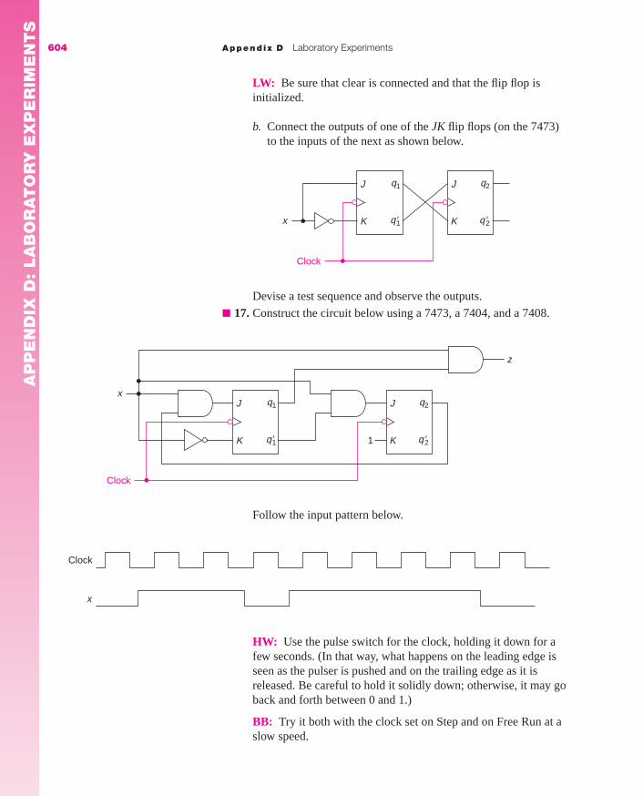
Clock
x
K1 q2�q1�K
J q2
x
z
J q1
Clock
LW: Be sure that clear is connected and that the flip flop isinitialized.
b. Connect the outputs of one of the JK flip flops (on the 7473)to the inputs of the next as shown below.
Devise a test sequence and observe the outputs.
■ 17. Construct the circuit below using a 7473, a 7404, and a 7408.
K q2�q1�K
J q2
x
J q1
Clock
604 Append ix D Laboratory Experiments
HW: Use the pulse switch for the clock, holding it down for afew seconds. (In that way, what happens on the leading edge isseen as the pulser is pushed and on the trailing edge as it isreleased. Be careful to hold it solidly down; otherwise, it may goback and forth between 0 and 1.)
BB: Try it both with the clock set on Step and on Free Run at aslow speed.
Follow the input pattern below.
AP
PE
ND
IX D
: LA
BO
RA
TO
RY
EX
PE
RIM
EN
TS
mar91647_apd_587_611.qxd 12/2/08 5:03 PM Page 604

LW: Connect a switch to x and set the clock to the slowestspeed. Label the clock, x, q1, and q2 so that the behavior can bedisplayed. Manipulate the switch so that the input patterndescribed in the problem is obtained. Stop the display when theend is reached and print out the timing diagram.*
■ 18. a. Construct the circuit of Exercise 8a (at the end of Chapter 6)and test it.
b. Construct the circuit of Exercise 8b (at the end of Chapter 6)and test it.
D.4.4 Experiments Based on Chapter 7 Material
■ 19. For each of the state tables in the following exercises of Chap-ter 7, design, build, and test a circuit using NAND gates and
i. D flip flopsii. JK flip flops
a. 7.2ab. 7.2dc. 7.2fd. 7.3ce. 7.3e
■ 20. Construct a synchronous base-12 counter using JK flip flops anda NAND gate.
■ 21. Construct a synchronous counter using D flip flops and NANDgates that goes through the sequence
i. 1 3 5 7 6 4 2 0 and repeat.ii. 1 3 4 7 2 6 0 and repeat.iii. 6 5 4 3 2 1 and repeat.iv. 1 3 4 7 6 and repeat.v. 1 2 4 5 0 6 and repeat.
vi. 1 4 0 3 5 2 and repeat.
Set the clock at its lowest speed.
a. Display the results on three lights.b. Connect the outputs to one of the seven-segment displays.
(Of course, the first bit of the display input is 0. Be sure toconnect the enable input for that display.)
HW: In the IDL-800, the clock speed cannot be made slowenough. Add a JK flip flop that is connected to change state everyclock period. The output of that flip flop will be a square wave athalf the frequency of the input. Use that to drive the display.
D.4 A Set of Logic Design Experiments 605
*To print, click on the timing display and choose Print Timing from the File menu. It isalso possible to Select All and copy the timing to another document.
AP
PE
ND
IX D
: LA
BO
RA
TO
RY
EX
PE
RIM
EN
TS
mar91647_apd_587_611.qxd 12/2/08 5:03 PM Page 605

■ 22. Build an asynchronous decade counter using JK flip flops andNAND gates.
HW, BB, LW: Display the results on a seven-segment display.
LW: Connect a switch to the CLR� input to reset the counter;that must be done at the beginning. Set the delay through eachof the flip flops at 3. (Do this by highlighting all of them,pulling down Simulation Params from the Simulate menu, andchanging the delay from 1 to 3. Watch the timing trace and seethat the counter reaches its state well into the clock period.Also, the counter reaches 10 and remains there for a shortperiod.
Magnify the display (by clicking �� on the SimulatorPalette two or three times) and determine when the answer isstable relative to the trailing edge of the clock and how long thesystem stays in state 10. (Note that by clicking on the timingdisplay, a vertical line will appear at that point. That will helpmeasure the timing more accurately.)
D.4.5 Experiments Based on Chapter 8 Material
■ 23. Using a 74164 shift register and a minimum number of AND,OR, and NOT gates, design and build a system that producesan output of 1 when the last nine inputs were 0.
HW, BB, LW: Use a pulser for the clock and a switch for theinput.
■ 24. Design a serial adder to add two 4-bit numbers. Each number isstored in a 7495 shift register.
FullAdder
Shift Registers
Flip Flop
c
606 Append ix D Laboratory Experiments
AP
PE
ND
IX D
: LA
BO
RA
TO
RY
EX
PE
RIM
EN
TS
mar91647_apd_587_611.qxd 12/2/08 5:03 PM Page 606
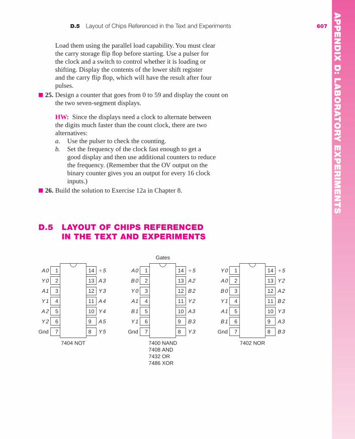
Load them using the parallel load capability. You must clearthe carry storage flip flop before starting. Use a pulser forthe clock and a switch to control whether it is loading orshifting. Display the contents of the lower shift registerand the carry flip flop, which will have the result after fourpulses.
■ 25. Design a counter that goes from 0 to 59 and display the count onthe two seven-segment displays.
HW: Since the displays need a clock to alternate betweenthe digits much faster than the count clock, there are twoalternatives:a. Use the pulser to check the counting.b. Set the frequency of the clock fast enough to get a
good display and then use additional counters to reducethe frequency. (Remember that the OV output on thebinary counter gives you an output for every 16 clockinputs.)
■ 26. Build the solution to Exercise 12a in Chapter 8.
D.5 LAYOUT OF CHIPS REFERENCEDIN THE TEXT AND EXPERIMENTS
D.5 Layout of Chips Referenced in the Text and Experiments 607
14
13
12
11
10
9
8
�5
A3
Y 3
A 4
Y4
A 5
Y 5
1
2
3
4
5
6
7
A0
Y 0
A1
Y 1
A 2
Y 2
Gnd
7404 NOT
14
13
12
11
10
9
8
�5
A2
B 2
Y2
A3
B 3
Y 3
1
2
3
4
5
6
7
A0
B 0
Y 0
A1
B1
Y 1
Gnd
7400 NAND7408 AND7432 OR7486 XOR
Gates
14
13
12
11
10
9
8
�5
Y2
A2
B 2
Y 3
A3
B 3
1
2
3
4
5
6
7
Y 0
A0
B 0
Y 1
A1
B1
Gnd
7402 NOR
AP
PE
ND
IX D
: LA
BO
RA
TO
RY
EX
PE
RIM
EN
TS
mar91647_apd_587_611.qxd 12/2/08 5:03 PM Page 607

608 Append ix D Laboratory Experiments
16
15
14
13
12
11
10
�5
Y 0 �
Y 1 �
Y 2 �
Y 3 �
Y 4 �
Y 5 �
1
2
3
4
5
6
7
A
B
C
EN 3 �
EN 2 �
EN1
Y 7 �
9 Y 6 �8Gnd
74138
16
15
14
13
12
11
10
�5
ENB1 �
ENB2 �
A
YB 3�
YB2 �
YB1 �
1
2
3
4
5
6
7
ENA1
ENA2�
B
YA3�
YA 2 �
YA1 �
YA0 �
9 YB0 �8Gnd
74155
24
23
22
21
20
19
18
�5
A
B
C
D
EN1 �
EN2 �
1
2
3
4
5
6
7
Y 0 �
Y 1 �
Y 2 �
Y 3 �
Y 4 �
Y 5 �
Y 6�
17 Y 15 �8Y 7 �
16
15
14
Y 14 �
Y 13 �
Y 12 �
0
10
11
Y 8 �
Y 9 �
Y 10 �
13 Y 11 �12Gnd
74154
Decoders
Adders Comparator
7483
14
13
12
11
10
9
8
�5
C 0
Y 0
A2
B 2
C 2
Y2
1
2
3
4
5
6
7
A0
B 0
A1
B1
C1
Y 1
Gnd
7410 NAND7411 AND7427 NOR
14
13
12
11
10
9
8
�5
A1
B 1
C 1
D1
Y 1
1
2
3
4
5
6
7
A0
B 0
C 0
D 0
Y 0
Gnd
7420 NAND7421 AND
14
13
12
11
10
9
8
�5
G
H
Y
1
2
3
4
5
6
7
A
B
C
D
E
F
Gnd
7430 NAND
16
15
14
13
12
11
10
9
Cout
Cout
Cin
Cin
Gnd
Gnd
B1
A1B2
A2
1
2
3
4
5
6
7
8
A4 B4
A3
B3
�5
�5
A1 is one input to gate 1, B1 is the second input, . . . ; Y 1 is the output.Unlabeled pins are not connected.
�2
�3 �4
�1
74283
16
15
14
13
12
11
10
9
B4
1
2
3
4
5
6
7
8
B3B2
A2 A3
A1 A4
B1
�1 �3
�2
�4
Gnd
�5
7485
16
15
14
13
12
11
10
9
B2
B1
1
2
3
4
5
6
7
8
A4
A1
INA�B
INA�B
INA�B
OUTA�B
OUTA�B
OUTA�B
B4
A3
A2
B3AP
PE
ND
IX D
: LA
BO
RA
TO
RY
EX
PE
RIM
EN
TS
mar91647_apd_587_611.qxd 12/2/08 5:03 PM Page 608

D.5 Layout of Chips Referenced in the Text and Experiments 609
16
15
14
13
12
11
10
�5
D
3�
2 �
1 �
9 �
1
2
3
4
5
6
7
4 �
5 �
6 �
7 �
8 �
C
B
9 A8Gnd
Priority Encoder
14
13
12
11
10
9
8
�5
g
f
b
c
d
1
2
3
4
5
6
7
B
C
EN�
D
A
e
Gnd
Seven-SegmentDecoder/Driver
7449
74147
a
16
15
14
13
12
11
10
�5
A4
A5
A6
A7
S0
S1
1
2
3
4
5
6
7
A3
A2
A1
A0
Y
Y�
EN�
9 S28Gnd
74151
16
15
14
13
12
11
10
�5
EN �
D 0
D1
YD
C 0
C1
1
2
3
4
5
6
7
S
A0
A1
YA
B0
B1
YB
9 YC8Gnd
74157
16
15
14
13
12
11
10
�5
ENB�
S0
B 3
B 2
B1
B 0
1
2
3
4
5
6
7
ENA�
S1
A3
A2
A1
A0
YA
9 YB8Gnd
74153
Multiplexers
16
15
14
13
12
11
10
K 1
Q 1
Q 1�
Gnd
K 2
Q 2
Q 2 �
1
2
3
4
5
6
7
Ck1 �
PRE1 �
CLR1 �
J1
�5
Ck2 �
PRE 2 �
9 J 28CLR2 �
7476
14
13
12
11
10
9
8
�5
CLR 2 �
D 2
Ck2
PRE 2 �
Q 2
Q 2 �
1
2
3
4
5
6
7
CLR 1�
D1
Ck1
PRE 1�
Q1
Q1�
Gnd
7474
Flip Flops
14
13
12
11
10
9
8
J 1
Q 1 �
Q 1
Gnd
K 2
Q 2
Q 2 �
1
2
3
4
5
6
7
Ck1�
CLR1�
K1
�5
Ck2 �
CLR 2 �
J 2
7473★
*WinBreadboard includes the 7473A, for which the connections for J1 and K1 areinterchanged, as are those for J2 and K2.
AP
PE
ND
IX D
: LA
BO
RA
TO
RY
EX
PE
RIM
EN
TS
mar91647_apd_587_611.qxd 12/2/08 5:03 PM Page 609

610 Append ix D Laboratory Experiments
16
15
14
13
12
11
10
�5
EN �
IN3
IN2
IN1
IN0
SIN
1
2
3
4
5
6
7
LD
Ck
IN4
IN 5
IN 6
IN 7
Q 7 �
9 Q 78Gnd
74165
16
15
14
13
12
11
10
�5
LD �
IN7
Q 7
IN 6
IN 5
IN 6
1
2
3
4
5
6
7
SIN
IN 0
IN1
IN 2
IN 3
EN �
Ck
9 CLR�8Gnd
74166
16
15
14
13
12
11
10
�5
Q 0
Q 1
Q 2
Q 3
Ck
S1
1
2
3
4
5
6
7
CLR�
RS
IN0
IN 1
IN 2
IN 3
LS
9 S08Gnd
74194
Shift Registers
16
15
14
13
12
11
10
�5
Q 5
D 5
D 4
Q 4
D 3
Q 3
1
2
3
4
5
6
7
CLR�
Q 0
D 0
Q 1
D1
Q 2
D 2
9 Ck8Gnd
74174
16
15
14
13
12
11
10
�5
Q 3
D 3
D 2
Q 3 �
Q 2 �
Q 2
1
2
3
4
5
6
7
CLR�
Q 0
Q 0 �
D 0
D1
Q1 �
Q1
9 Ck8Gnd
74175
16
15
14
13
12
11
10
CLR�
Q 0
Q 1
Q 2
Gnd
Q 3
Q 4
1
2
3
4
5
6
7
Ck
IN 0
IN1
IN 2
�5
IN 3
IN 4
9 S8LD
7496
Shift Registers
14
13
12
11
10
9
8
�5
Q 0
Q 1
Q 2
Q 3
CkS
CkL
1
2
3
4
5
6
7
SIN
IN 0
IN1
IN 2
IN 3
S
Gnd
7495
S � 0: Shift, S � 1: LoadCkS: Shift clockCkL: Load clockSIN: Serial left bit Input
14
13
12
11
10
9
8
�5
Q 7
Q 6
Q 5
Q 4
CLR�
Ck
1
2
3
4
5
6
7
A
B
Q 0
Q 1
Q 2
Q 3
Gnd
74164
AP
PE
ND
IX D
: LA
BO
RA
TO
RY
EX
PE
RIM
EN
TS
mar91647_apd_587_611.qxd 12/2/08 5:03 PM Page 610
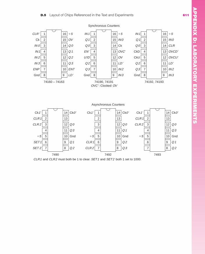
D.5 Layout of Chips Referenced in the Text and Experiments 611
16
15
14
13
12
11
10
�5
OV
Q 0
Q 1
Q 2
Q 3
ENT
1
2
3
4
5
6
7
CLR �
Ck
IN 0
IN1
IN 2
IN 3
ENP
9 LD �8Gnd
74160 – 74163
16
15
14
13
12
11
10
�5
IN0
Ck
OVC�
OV
LD �
IN2
1
2
3
4
5
6
7
IN1
Q 1
Q 0
EN �
U�/D
Q 2
Q 3
9 IN38Gnd
74190, 74191OVC �: Clocked OV
Synchronous Counters
16
15
14
13
12
11
10
�5
IN0
CLR
OVCD �
OVCU�
LD �
IN2
1
2
3
4
5
6
7
IN1
Q 1
Q 0
CkD
CkU
Q 2
Q 3
9 IN38Gnd
74192, 74193
14
13
12
11
10
9
8
Ck0 �
Q 0
Q 3
Gnd
Q 1
Q 2
1
2
3
4
5
6
7
Ck1�
CLR 1
CLR 2
�5
SET1
SET 2
7490
CLR1 and CLR2 must both be 1 to clear. SET1 and SET2 both 1 set to 1000.
14
13
12
11
10
9
8
Ck0 �
Q 0
Q 3
Gnd
Q 1
Q 2
1
2
3
4
5
6
7
Ck1 �
CLR 1
CLR 2
�5
7493
14
13
12
11
10
9
8
Ck0 �
Q 0
Q 1
Gnd
Q 2
Q 3
1
2
3
4
5
6
7
Ck1 �
�5
CLR 1
CLR 2
7492
Asynchronous Counters
AP
PE
ND
IX D
: LA
BO
RA
TO
RY
EX
PE
RIM
EN
TS
mar91647_apd_587_611.qxd 12/2/08 5:03 PM Page 611
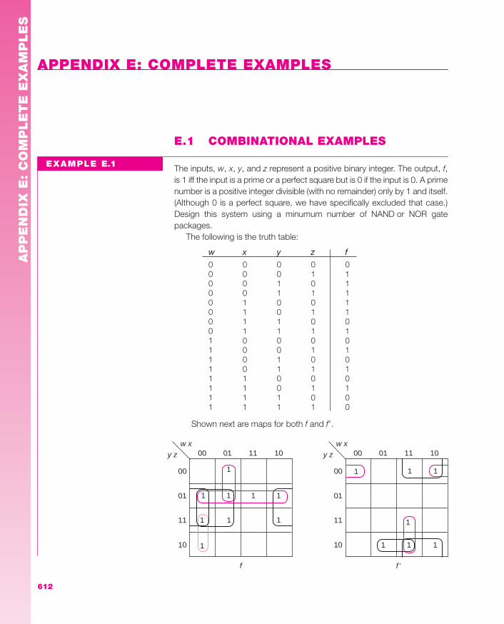
612
E.1 COMBINATIONAL EXAMPLES
The inputs, w, x, y, and z represent a positive binary integer. The output, f,is 1 iff the input is a prime or a perfect square but is 0 if the input is 0. A primenumber is a positive integer divisible (with no remainder) only by 1 and itself. (Although 0 is a perfect square, we have specifically excluded that case.)Design this system using a minumum number of NAND or NOR gate packages.
The following is the truth table:
w x y z f0 0 0 0 00 0 0 1 10 0 1 0 10 0 1 1 10 1 0 0 10 1 0 1 10 1 1 0 00 1 1 1 11 0 0 0 01 0 0 1 11 0 1 0 01 0 1 1 11 1 0 0 01 1 0 1 11 1 1 0 01 1 1 1 0
Shown next are maps for both f and f�.
APPENDIX E: COMPLETE EXAMPLES
00 01 11 10
00
01
11
10
w x
y z
1 11 1
1
1 1 1
1
00 01 11 10
00
01
11
10
w x
y z
11
1
1 11
1
f f �
EXAMPLE E.1
AP
PE
ND
IX E
: C
OM
PLE
TE
EX
AM
PLE
S
mar91647_ape_612_628.qxd 12/5/08 9:57 AM Page 612

E.1 Combinational Examples 613
f = w�z + x�z + y�z + w�xy� + w�x�yf� = wz� + xyz� + wxy + x�y�z�
f = (w� + z) (x� + y� + z) (w� + x� + y�) (x + y + z)
The two-level NAND gate implementation requires 3 two-input gates, 2 three-input gates, and 1 five-input gate, three packages. The two-levelNOR uses 1 four-input gate, 3 three-input gates, and 1 two-input gate, onlytwo packages (since the two-input gate uses the leftover four-input one).
The NOR implementation is
f
w �
w �
x �
x �
y �
y �
z
z
y z
x
We could reduce the number of packages using NAND gates to two byfactoring z from the second and third terms and w� from the others
f = z (x� + y�) + w� (z + xy� + x�y) = z (x� + y�) + w� [z + (x + y) (x� + y�)]
That results in the following circuit, which uses only 7 two-input NANDgates (two packages).
f
z � w �
x �
y �
z
y
x
AP
PE
ND
IX E
: CO
MP
LE
TE
EX
AM
PLE
S
mar91647_ape_612_628.qxd 12/2/08 5:03 PM Page 613

614 Append ix E Complete Examples
The inputs represent a decimal digit in 2421 code (See Table 1.7). In thatweighted code, each of the unused combinations also represent one of thedecimal digits. Design a system with two outputs, f and g, such that f is 1 iffthe digit represented is a multiple of 2 or 3 (or both) and g is 1 if this is notthe normally used code. For example, 7 is normally coded 1101 (2 + 4 + 0 + 1) and the code 0111 (0 + 4 + 2 + 1) is unused. Thus, f = 0 in both rows,but g = 0 for row 1101 and g = 1 for row 0111.
A truth table for these functions is shown next.
w x y z Digit f g
0 0 0 0 0 0 00 0 0 1 1 0 00 0 1 0 2 1 00 0 1 1 3 1 00 1 0 0 4 1 00 1 0 1 5 0 10 1 1 0 6 1 10 1 1 1 7 0 11 0 0 0 2 1 11 0 0 1 3 1 11 0 1 0 4 1 11 0 1 1 5 0 01 1 0 0 6 1 01 1 0 1 7 0 01 1 1 0 8 1 01 1 1 1 9 1 0
We will start by getting sum of products representations, leading towardNAND gate solutions. The functions f and g are mapped below.
EXAMPLE E.2
00 01 11 10
00
01
11
10
w x
y z
1
111
1 1
1 1 11
00 01 11 10
00
01
11
10
w x
y z
1
1
11
1
1
f g
AP
PE
ND
IX E
: C
OM
PLE
TE
EX
AM
PLE
S
mar91647_ape_612_628.qxd 12/2/08 5:03 PM Page 614

E.1 Combinational Examples 615
The minimum sum of products expressions for f and g are
f = xz� + w�x�y + wxy + wx�y� + {wz� or yz�}g = w�xy + w�xz + wx�y� + wx�z�
A two-level solution would require 2 two-input gates, 6 three-input gates(since we could share the gate producing wx�y�), 1 four-input gate, and 1 five-input gate. That would require five packages.
We could take advantage of sharing, by using wx�z� instead of the lastterm in f. That would save a two-input gate, reducing the package count tofour, since the two-input gate could be implemented using the extra four-input one.
Each function could be implemented with only two-input gates, shar-ing two, but requiring a total of 17 gates (five packages):
f = z� (x + y) + [w� +(x + y�) (x� + y)] [w + x�y]g = w� (xy + xz) + w (x�y� + x�z�)
Another approach, using two- and three-input gates comes from thefollowing equations:
f = xz� + y (w�x� + wx) + wx� (y� + z�)g = w�x (y + z) + wx� (y� + z�)
resulting in a circuit using 3 three-input gates and 8 two-input gates, onlythree packages. The circuit is shown below.
w �x �
x �
x �z �
wx
y �
y
x
z
y
w
w
g
f
z �
AP
PE
ND
IX E
: CO
MP
LE
TE
EX
AM
PLE
S
mar91647_ape_612_628.qxd 12/2/08 5:03 PM Page 615

616 Append ix E Complete Examples
f� = w�x�y� + w�xz + xy�z + wx�yzg� = w�x� + wx + {w�y�z� or xy�z�} + {wyz or x�yz}
or, choosing the first of the alternates,
f = (w + x + y) (w + x� + z�) (x� + y + z�) (w� + x + y� + z�)g = (w + x) (w� + x�) (w + y + z) (w� + y� + z�)
The two-level solution requires 2 two-input gates, 5 three-input gates, and3 four-input gates, which could be implemented with four packages. Thereis no way to do it with all two-input gates or with less than four packages.
00 01 11 10
00
01
11
10
w x
y z
11 1
1
1 1
00 01 11 10
00
01
11
10
w x
y z
11
1 1
1
1
1
1
1
f � g �
f
w �
x �
xy �z �
x �yz �
x y
w
w
z �
g
w
y
x �w �
x
w �y �z �
w
z
AP
PE
ND
IX E
: C
OM
PLE
TE
EX
AM
PLE
S
Next, we will look at product of sums expressions and NOR gateimplementations. The maps of f� and g� are shown next.
mar91647_ape_612_628.qxd 12/5/08 9:53 AM Page 616

the point of view of this problem). It can be a strike, a foul ball, a ball, oranything else that will end this batter’s turn (such as a hit or a fly out).
A foul ball is considered a strike, except when there are already twostrikes, in which case the number of strikes remains 2. The output is toindicate the number of balls and strikes after this pitch unless the bat-ter’s turn is over. If the batter’s turn is over for any reason, the outputshould indicate 0 balls and 0 strikes.
Show the code for the inputs (there should be 6—2 for the whathappened on that pitch, 2 for the number of balls, and 2 for the numberof strikes) and for the outputs (there should be 5—3 for balls and 2 forstrikes). Then show maps and an implementation using NAND gates.
Comment: A more complete problem would include the number of outs,but that would involve two more inputs for the number of outs before thepitch and at least one more input column for pitch outcome, since wewould need to differentiate between hits and outs, as well as doubleplays and players out stealing.
We will use the first two inputs, a and b, to indicate the number ofballs, the next two, c and d, to indicate the number of strikes (which isnever 3), and the last two, e and f, to indicate the outcome of the pitch,as follows:
e f Outcome0 0 Strike0 1 Foul1 0 Ball1 1 Anything else
The outputs, w and x, are the number of balls after the pitch, and y andz are the number of strikes after the pitch.
The six variable maps are shown next. The layers correspond to thenumber of balls; the columns are the number of strikes. Since there arenever three strikes before a pitch, the 11 column is all don’t cares.
E.1 Combinational Examples 617
The problem is to design a ball and strike counter for baseball. Theinputs are how many balls (0, 1, 2, 3) before this pitch, how many strikes(0, 1, 2) before this pitch, and what happens on this pitch. The outputsare how many balls after this pitch (0, 1, 2, 3) or how many strikes afterthis pitch (0, 1, 2). In baseball, there are four outcomes of any pitch (from
EXAMPLE E.3
AP
PE
ND
IX E
: CO
MP
LE
TE
EX
AM
PLE
S
mar91647_ape_612_628.qxd 12/2/08 5:03 PM Page 617

618 Append ix E Complete Examples
00
0 0 0 1
01 11 10
00
01
11
10
c de f
X
X
X
X
X
X
X
X
00 01 11 10
00
01
11
10
c de f
111
00
1 1 1 0
0 0 0 1 1 1 1 0
0 0 0 1 1 1 1 0
0 0 0 1 1 1 1 0
01 11 10
00
01
11
10
c de f
X
X
X
X
X
X
X
X
00 01 11 10
00
01
11
10
c de f
111
11
1 1 11
11
11
00 01 11 10
00
01
11
10
c de f
X
X
X
X
X
X
00 01 11 10
00
01
11
10
c de f 00 01 11 10
00
01
11
10
c de f
X
X
X
X
X
X
X
X
00 01 11 10
00
01
11
10
c de f
111
11
1 11
X 111
X11
1 11
00 01 11 10
00
01
11
10
c de f
X 1
X
1
1
11
1
X
X
X
X
X
X
00 01 11 10
00
01
11
10
c de f
1
00 01 11 10
00
01
11
10
c de f
X
X
X
X
X
X
X
X
00 01 11 10
00
01
11
10
c de f
1
1
1 1 1
1
1
00 01 11 10
00
01
11
10
c de f
X 1
X
X
X1
X
X
X
X
00 01 11 10
00
01
11
10
c de f
1
00 01 11 10
00
01
11
10
c de f
X
X
X
X
X
X
X
X
00 01 11 10
00
01
11
10
c de f
1
1
1
1
1 1
1
1
1
a b
a b
a b
a b
W
X
Y
Z
The resulting minimum sum of product equations are
w = a�bef� + ab�ef� + ac�e� + ae�fx = b�ef� + bc�e� + be�fy = de� + ce�f + a�bcef� + ab�cef�z = c�d�e� + a�def� + b�def�
There are no common prime implicants that take advantage of sharing (asin Section 3.8). Implementing them directly requires
AP
PE
ND
IX E
: C
OM
PLE
TE
EX
AM
PLE
S
mar91647_ape_612_628.qxd 12/2/08 5:03 PM Page 618
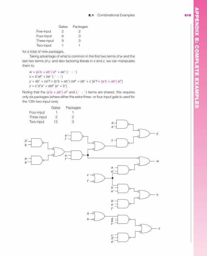
y
w
x
z
e �
e �
e �
f �
f �
c �d �e �
b �
f �
e �
a �
b
b �
a
c
a
b
e
a
d e
b
d
c
f �
f
e
Gates PackagesFive-input 2 2Four-input 6 3Three-input 9 3Two-input 1 1
for a total of nine packages.Taking advantage of what is common in the first two terms of w and the
last two terms of y, and also factoring literals in x and z, we can manipulatethem to
w = (a�b + ab�) ef� + ae� (c� + f )x = b�ef� + be� (c� + f )y = de� + ce�f + (a�b + ab�) cef� = de� + c [e�f + (a�b + ab�) ef�]z = c�d�e� + def� (a� + b�)
Noting that the (a�b + ab�) ef� and (c� + f ) terms are shared, this requiresonly six packages (where either the extra three- or four-input gate is used forthe 13th two-input one).
Gates PackagesFour-input 1 1Three-input 5 2Two-input 13 3
E.1 Combinational Examples 619
AP
PE
ND
IX E
: CO
MP
LE
TE
EX
AM
PLE
S
mar91647_ape_612_628.qxd 12/2/08 5:03 PM Page 619
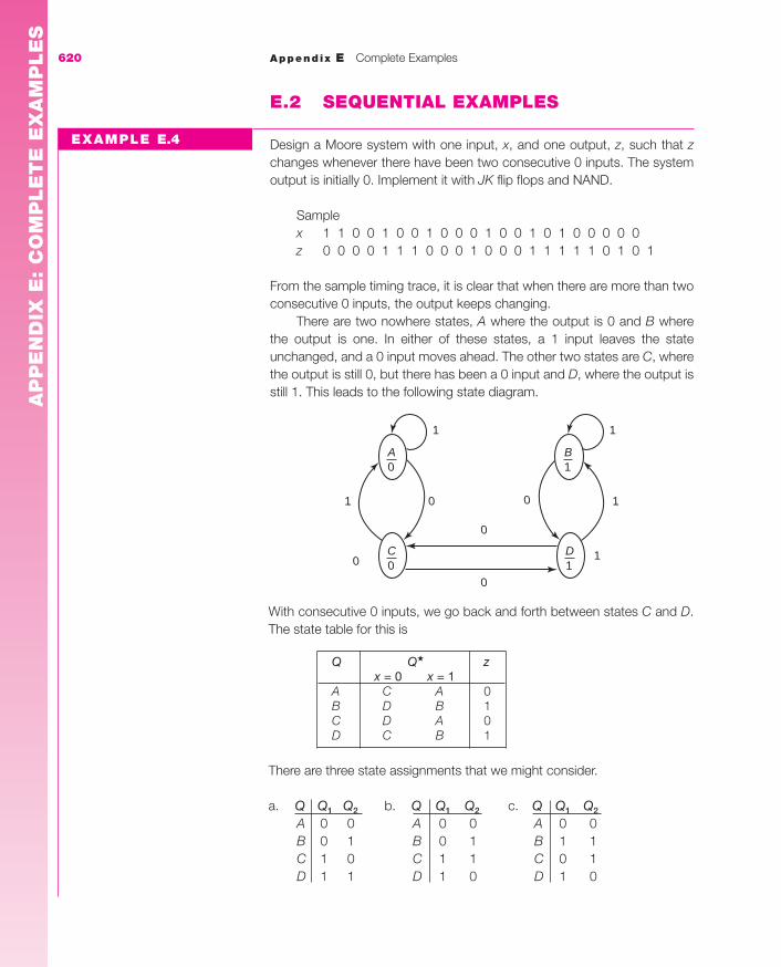
620 Append ix E Complete Examples
E.2 SEQUENTIAL EXAMPLES
Design a Moore system with one input, x, and one output, z, such that zchanges whenever there have been two consecutive 0 inputs. The systemoutput is initially 0. Implement it with JK flip flops and NAND.
Samplex 1 1 0 0 1 0 0 1 0 0 0 1 0 0 1 0 1 0 0 0 0 0 z 0 0 0 0 1 1 1 0 0 0 1 0 0 0 1 1 1 1 1 0 1 0 1
From the sample timing trace, it is clear that when there are more than twoconsecutive 0 inputs, the output keeps changing.
There are two nowhere states, A where the output is 0 and B where the output is one. In either of these states, a 1 input leaves the stateunchanged, and a 0 input moves ahead. The other two states are C, wherethe output is still 0, but there has been a 0 input and D, where the output isstill 1. This leads to the following state diagram.
EXAMPLE E.4
0
0
0
0
0
1 1
11
1
A0
B1
D1
C0
With consecutive 0 inputs, we go back and forth between states C and D.The state table for this is
Q Q� zx = 0 x = 1
A C A 0B D B 1C D A 0D C B 1
There are three state assignments that we might consider.
a. Q Q1 Q2 b. Q Q1 Q2 c. Q Q1 Q2
A 0 0 A 0 0 A 0 0B 0 1 B 0 1 B 1 1C 1 0 C 1 1 C 0 1D 1 1 D 1 0 D 1 0
AP
PE
ND
IX E
: C
OM
PLE
TE
EX
AM
PLE
S
mar91647_ape_612_628.qxd 12/5/08 9:53 AM Page 620

E.2 Sequential Examples 621
*In Chapter 9, we will see that this assignment for Q1 will produce the simplest inputs forthat JK flip flop.
The first and third assignments require no output logic; z = Q2 for assign-ment a and z = Q1 for assignment c. For assignment b, z = Q1� Q2 + Q1 Q2�,requiring three gates. We will complete the design using assignments aand c.
a. c.x Q1 Q2 Q1
� Q1� Q1
� Q2�
0 0 0 1 0 0 10 0 1 1 1 1 00 1 0 1 1 0 10 1 1 1 0 1 01 0 0 0 0 0 01 0 1 0 1 0 01 1 0 0 0 1 11 1 1 0 1 1 1
For assignment a, the maps are
0 1
00
01
11
10
x
1
1
1
1
0 1
00
01
11
10
x
Q1 Q2Q1 Q2
1
1
11
Q1� Q2
�
J1 = x� K1 = x J2 = K2 = x� Q1 z = Q2
This requires 1 two-input NAND and two inverters.*
For assignment c, the maps are
0 1
00
01
11
10
x
1
1 1
1
0 1
00
01
11
10
x
Q1 Q2Q1 Q2
1
1
1
1
J1 = K1 = x� Q2� J2 = x� + Q1 K2 = x� + Q1 z = Q1
AP
PE
ND
IX E
: CO
MP
LE
TE
EX
AM
PLE
S
mar91647_ape_612_628.qxd 12/2/08 5:03 PM Page 621

This requires 3 two-input NANDs and two inverters. (Assignment b wouldrequire 4 two-input NANDs and one inverter).
The circuit for assignment a becomes
622 Append ix E Complete Examples
x
Z
CLOCK
CLEAR�
J Q1
Q1K
J Q2
Q2K� �
We are designing an automatic light controller for a small room, one that holdsa maximum of three people. There is a signal that is 1 for one clock period online x1 whenever someone enters the room and a similar signal on line x2 whensomeone leaves. When the room is empty, the light in the room is off; whenanyone is in the room, the light is on. Output z1 controls that light. If the roomis full, a red light, controlled by output line z2, outside the room is lit.
We need an up/down counter, AB, initialized to 0, to keep track of thenumber of people in the room. It is somewhat different from the one dis-cussed in Example 7.8 because there are separate inputs for counting upand counting down.
The state table is thus
AB x1x2 A� B� z1z2
0 0 0 1 1 0 1 10 0 0 0 X X 0 1 0 0 0 00 1 0 1 0 0 1 0 0 1 1 01 0 1 0 0 1 1 1 1 0 1 01 1 1 1 1 0 X X 1 1 1 1
The counter goes up when someone enters (the 10 column) and downwhen someone leaves (the 01 column). We assume that no one enterswhen the room is full and no one leaves when it is empty (accounting for thedon’t cares). The first output is 1 whenever the count is not 0, and the sec-ond is 1 when the count is 3. (This is a Moore system.)
The equations for the outputs can read from the state table.
z1 = A + B z2 = AB
EXAMPLE E.5
AP
PE
ND
IX E
: C
OM
PLE
TE
EX
AM
PLE
S
where the NOT gate is needed for the inputs to Q2 to create an AND. Also,a CLEAR� signal is shown to initialize the system to state 00.
mar91647_ape_612_628.qxd 12/2/08 5:03 PM Page 622

E.2 Sequential Examples 623
The maps for the next state, with the J sections shaded, are shown next.
00 01 11 10
00
01
11
10
x1 x2 x1 x2
A B
X
1
1 11 X
1 1 1
00 01 11 10
00
01
11
10
A B
1
1 1 X
1
11
1X
A★ B★
JA = x1 x2� B KA = x1� x2 B� JB = KB = x1� x2 + x1 x2�
The circuit is shown next, with a CLEAR� to initialize it.
J B
B�K
J
x2
x1
A
A �K
CLOCK
CLEAR�
z1
z2
Design a Moore system using JK flip flops that produces a 1 output if theinput pattern has been 1 0 1 1
a. If overlapping is NOT allowed (5 states).b. If overlapping is allowed (5 states).c. Once the output is 1, it remains 1 as long as the pattern is
continuing (7 states).
EXAMPLE E.6
AP
PE
ND
IX E
: CO
MP
LE
TE
EX
AM
PLE
S
mar91647_ape_612_628.qxd 12/2/08 5:03 PM Page 623

Samplesx 0 0 1 0 1 1 0 1 1 1 0 1 1 0 1 1 0 0 za ? 0 0 0 0 0 1 0 0 0 0 0 0 1 0 0 0 0 0 0 0zb ? 0 0 0 0 0 1 0 0 1 0 0 0 1 0 0 1 0 0 0 0zc ? 0 0 0 0 0 1 1 1 1 0 0 0 1 1 1 1 1 0 0 0
All three start out the same way, where state A is nowhere, looking forthe first 1, state B is reached with the first 1, C is reached with the 0, D onthe second 1, and E is reached when the pattern is complete and the out-put is 1. The first state diagram shows the answers for parts a and b.
624 Append ix E Complete Examples
0
0
0
0
0
0
1
1 1
1
1
A0
C0
D0
E 1
B0
(no)
(over)
After getting to state E, a 1 input would be the first 1 in a new sequence(state B). If overlapping is not allowed, a 0 input leaves us nowhere, back instate A. If overlapping is allowed, we now have the 10 of a new pattern andgo to state C.
For part c, we need two new states. From E, a 0 input continues thepattern and should thus produce a 1 output. Then a 1 input keeps it going(to state G). Finally, another 1 gets us back to state G as shown below.
AP
PE
ND
IX E
: C
OM
PLE
TE
EX
AM
PLE
S
mar91647_ape_612_628.qxd 12/2/08 5:03 PM Page 624

We will next look at the implementation of this system using JK flip flops. Wewill consider two state assignments:
a. Q q1 q2 q3 b. Q q1 q2 q3
A 0 0 0 A 0 0 0B 0 0 1 B 0 1 0C 0 1 0 C 0 0 1D 0 1 1 D 0 1 1E 1 0 0 E 1 1 0F 1 0 1 F 1 0 1G 1 1 0 G 1 1 1
The first just assigns the states in numerical order. The second uses someinformation from Chapter 9. First, we will convert the state diagram to astate table and then create the truth table using the first assignment.
Q Q� zx = 0 x = 1
A A B 0B C B 0C A D 0D C E 0E F B 1F A G 1G C E 1
E.2 Sequential Examples 625
00
00
0
0
0
1
1
1
1
1
1
A0
C0
G 1
1
D0
E 1
B0
F 1
AP
PE
ND
IX E
: CO
MP
LE
TE
EX
AM
PLE
S
mar91647_ape_612_628.qxd 12/2/08 5:03 PM Page 625

The design truth table has 16 rows:
x q1 q2 q3 q1� q2
� q3� J1 K1 J2 K2 J3 K3
A 0 0 0 0 0 0 0 0 X 0 X 0 XB 0 0 0 1 0 1 0 0 X 1 X X 1C 0 0 1 0 0 0 0 0 X X 1 0 XD 0 0 1 1 0 1 0 0 X X 0 X 1E 0 1 0 0 1 0 1 X 0 0 X 1 XF 0 1 0 1 0 0 0 X 1 0 X X 1G 0 1 1 0 0 1 0 X 1 X 0 0 X
0 1 1 1 X X X X X X X X XA 1 0 0 0 0 0 1 0 X 0 X 1 XB 1 0 0 1 0 0 1 0 X 0 X X 0C 1 0 1 0 0 1 1 0 X X 0 1 XD 1 0 1 1 1 0 0 1 X X 1 X 1E 1 1 0 0 0 0 1 X 1 0 X 1 XF 1 1 0 1 1 1 0 X 0 1 X X 1G 1 1 1 0 1 0 0 X 0 X 1 0 X
1 1 1 1 X X X X X X X X X
After mapping these, we get
J1 = x q2 q3 K1 = x� q2 + x� q3 + x q2� q3�
J2 = x� q1� q3 + x q1 q3 K2 = x� q1� q3� + x q1 + x q3
J3 = q1 q2� + x q1� K3 = x + q1 + q2
Z = q1
This requires 8 two-input gates and 8 three-input gates plus the NOT for x�.Using the second assignment, we get the following design truth table:
x q1 q2 q3 q1� q2
� q3�
A 0 0 0 0 0 0 0C 0 0 0 1 0 0 0B 0 0 1 0 0 0 1D 0 0 1 1 0 0 1
0 1 0 0 X X XF 0 1 0 1 0 0 0E 0 1 1 0 1 0 1G 0 1 1 1 0 0 1A 1 0 0 0 0 1 0C 1 0 0 1 0 1 1B 1 0 1 0 0 1 0D 1 0 1 1 1 1 0
1 1 0 0 X X XF 1 1 0 1 1 1 1E 1 1 1 0 0 1 0G 1 1 1 1 1 1 0
We will map these and use the quick method.
626 Append ix E Complete Examples
AP
PE
ND
IX E
: C
OM
PLE
TE
EX
AM
PLE
S
mar91647_ape_612_628.qxd 12/2/08 5:03 PM Page 626

E.2 Sequential Examples 627
00 01 11 10
00
01
11
10
xq1
q2q3 q2q3
X X
1
1
1 1
00 01 11 10
00
01
11
10
1
1
1
1
1
1
1X X
00 01 11 10
00
01
11
10
1 1
1 1
1 1
X X
Q1★ Q2
★ Q3★
xq1 xq1
q2q3
The J sections of each of the maps are shaded, producing the equations
J1 = x q2 q3 K1 = x q3 + x� q3�
J2 = x K2 = x�
J3 = x� q2 K3 = x� q2� + x q2
Z = q1
This assignment requires only 7 two-input gates and 1 three-input gate plusthe NOT for x� (no three-input gates).
AP
PE
ND
IX E
: CO
MP
LE
TE
EX
AM
PLE
S
mar91647_ape_612_628.qxd 12/2/08 5:03 PM Page 627

mar91647_ape_612_628.qxd 12/2/08 5:03 PM Page 628

629
Aabsorption, 65active signals
high, 258low, 258
adder, 10, 252–255carry-look-ahead, 255carry-ripple, 252cascaded, 255chip layouts, 607–611decimal, 292–293four-bit, 10–11, 30, 264, 267full, 10, 58, 76–78, 250–252half, 11lab experiments, 599–601multi-bit, 252–255one-bit, 10, 76–78serial, 514–515Verilog, 289–292
adder/subtractor, 266adjacency, 44–45adjacent squares, 66algebra. See switching algebra
Boolean, 78–80algorithmic state machine (ASM) diagrams,
511–515Altera tool set, 4American Standard Code for Information
Interchange (ASCII), 17–18AND. See also gate
AND/OR/NOT implementation, 48–52arrays, 276–278defined, 38–39gate, 40wired, 274
arrays. See gate arraysassociative law, 39asynchronous counters, 447–450, 503–506
Bbase, 4binary arithmetic, 9-15
addition, 9-14binary to decimal conversion, 4–6digits, 1, 5decimal to binary conversion, 6–7error detecting and correcting codes,
301–304hexadecimal numbers, 8integers, 4signed numbers, 11–14subtraction, 14–15
binary coded decimal (BCD), 15–16, 22–23bits, 1, 3Boole, George, 78Boolean algebra, 37, 78–80breadboards, 27
hardware logic, 4, 567–591Macbreadboard, 4, 591–593Winbreadboard, 4, 591–593
bubble, 60bus, 275
controller design, 416, 461–464
Ccanonical product, 47canonical sum, 44carry-look-ahead adders, 255
INDEX
Note: Page numbers having the format 9-x indicate material in Chapter 9, which can be found online athttp://www.mhhe.com/marcovitz.
mar91647_ind_629_644.qxd 12/2/08 1:41 PM Page 629

cascadedadders, 255comparators, 256–268counters, 492–494
check bit, 302chips, 50. See also integrated circuitscircuits
integrated, 50 (see also integrated circuits)number of levels, 48–49
clear signal, 376–377clock, 2, 365clocked, 365coding
inputs and outputs, 30, 34–36, 416states, 417, 9-22 to 9-28
combinational systems, 2design process for, 29–37
common mistakes, 53, 67, 128commutative property, 39comparator, 256–258
chip layout, 608complement, 44. See also NOT
DeMorgan’s theorem, 52–54radix, 12two’s, 11–14
complete examplescombinational, 612–619sequential, 620–627
complex programmable logic devices (CPLD),510–511
consensus, 67–70. See also iterated consensusContinuing Examples (CE)
CE1, 29, 33–34, 57CE2, 29, 34–35, 57CE3, 29, 35, 58, 76–78, 250–252CE4, 29, 35–36, 293–301CE5, 29, 35CE6, 366–369, 415n, 450–452, 454CE7, 415, 452–454CE8, 415, 458–459CE9, 415, 442–445
CE10, 415–416, 446–447CE11, 416, 461–464
convertbinary to decimal, 4–6binary to hexadecimal, 8decimal to binary, 6–7decimal to hexadecimal, 8hexadecimal to decimal, 8
counter, 437–450application of, 499–506asynchronous, 447–450, 503–506chip layouts, 611decimal (decade), 441–442, 502–503enable signals, 499–500lab experiments, 605–607synchronous, 437–447, 499–503up/down, 439–440, 449–450,
502–503cover, 119CPLD (complex programmable logic device),
510–511
Ddecade counter, 441–442, 502–503decimal systems
BCD, 16–17 (see also binary coded decimal)
decoders, 258–267chip layouts, 608enable signals, 258–267implementation of logic functions,
263–267lab experiments, 601
delayadders, 251–255combinational systems, 250–252
delay flip flops (D), 372–377analysis, 380–390design techniques, 420–421PLDs and, 506–509
630 Index
mar91647_ind_629_644.qxd 12/2/08 1:41 PM Page 630

DeMorgan’s theorem, 52–54demultiplexer, 273–274design process
combinational systems, 29–37sequential systems, 416–418
design truth table, 418–420digital systems, 1distributive, 41–42don’t care conditions, 32–33, 112
iterated consensus, 206Karnaugh map, 135–139Quine-McCluskey, 204
driversseven-segment displays, 35–36, 293–301
dual, 40dual in-line packages (DIPs), 50
E8421 code, 16enable signals
counters, 499–503decoders, 258–267PLDs, 506–507shift registers, 496–497
encoders, 268–269chip layouts, 609priority, 268–269
English, 3equivalent, 9-1 to 9-3
partitions, 9-17 to 9-22tabular reduction, 9-3 to 9-10
erasable programmable read-only memories(EPROMs), 279
error detection/correction, 301–304essential prime implicant, 121
don’t care conditions, 135–136prime implicant tables, 208
excess 3 code, 16–17Exclusive-NOR gates, 63
comparators, 256–258
Exclusive-OR gates, 63–64comparators, 269–270
exercises, 7nexpressions
product of sums, 46–47sum of products, 43
Ffactoring, 41false outputs, 387–389fan-in, 253field programmable logic array, 276n, 279, 510finite state machines (FSMs), 365. See also
state machines, sequential systems5421 code, 16–17five-variable maps, 143–149flip flops, 366, 371–380
asynchronous clear inputs, 376–377chip layouts, 609–610delay, 372–377, 420–422 (see also delay flip
flops (D))design table, 420–425design techniques for, 420–436experiments, 603–605JK, 378–379, 422–423, 425–430 (see also
JK flip flops)leading-edge triggered, 373–375master/slave, 372PLDs, 506–511quick method, 428–430registers, 493 (see also registers)Set-Reset, 377–378, 423–424 (see also Set-
Reset (SR) flip flop)state, 373static clear input, 376–377Toggle, 378–379, 424–425 (see also Toggle
(T) flip flops)trailing-edge triggered, 371–380
FPGA (field programmable gate array),276n, 279
Index 631
mar91647_ind_629_644.qxd 12/2/08 1:41 PM Page 631

full adder, 10, 58, 76–78, 250–252functionally complete, 59functions
complement of, 52–54multiple output, 150–161, 216, 226simplification, 65–70
fuse, 279
Ggate, 32, 39
AND, 39chip layouts, 607–608delay, 250–252Exclusive-OR, 63Exclusive-NOR, 63function implementation, 48–52, 59–65lab experiments, 598–600latches, 370–371NAND, 59–62NOR, 61–62NOT, 40OR, 39
gate arrays, 249, 276–288field programmable, 276nPAL design, 286–288PLA design, 281–284PLDs, 506–511ROM design, 280–281
generate, carry, 255glitch, 251, 387–388Gray code, 18
Hhalf adders, 11Hamming code, 301–304Hamming distance, 302hardware design language (HDL), 289–292,
516–517
hazard, 251hexadecimal, 8hot, 515
Iidempotency, 41identity, 41implicant, 118–119. See also prime implicantincluded in, 204–205Inclusive-OR, 50incompletely specified functions, 32. See also
don’t care conditionsInstruction Register, 519–521integrated circuits (ICs), 50
7400 series, 51 (see also 7400 series chips)
inversion, 40involution, 41isolated, 121
Map Method 1, 122–130iterated consensus, 201
multiple output, 219–222one output, 204–207prime implicant tables, 208–216,
222–226iterative systems, 249, 250–258
JJK flip flops (JK), 378–377. See also flip flops
analysis, 381–390design techniques, 422–423, 425–430
KKarnaugh map, 111–161
algebraic simplification, 543–547don’t cares, 135–139five-variable, 143–149
632 Index
mar91647_ind_629_644.qxd 12/2/08 1:41 PM Page 632
Map Method 1, 122–130Map Method 2, 130–135multiple output, 150–161product of sums, 140–143six-variable, 144, 149sum of products, 122–139
Karnaugh, Maurice, 111
Llaboratory systems, 3
Altera, 4chip layout, 607–611experiments, 598–607hardware, 3, 583–587LogicWorks, 4, 589–594MacBreadboard, 4, 587–589WinBreadboard, 4, 587–589
large-scale integration (LSI), 51latches, 370–371levels, 48–49literal, 43LogicWorks, 593–598LUT (lookup table), 510–511
MMacBreadboard, 4, 591–593Map Method 1, 122–130Map Method 2, 130–135master/slave flip flop, 372maxterm, 46Mealy model, 369–370
analysis, 369–370ASM diagrams, 513–514false output (glitch), 387–388state diagrams, derivation of, 452–461
medium-scale integration (MSI), 51memory, 2, 364–365, 518–521. See also
sequential systems
minimumalgorithmic minimization, 201–226don’t care conditions, 135–139five/six variable maps, 143–149NAND gate networks, 72–78product of sums, 47, 140–143sum of products, 44
don’t cares, 135–139using the Karnaugh map, 121–135
minterm, 43Moore model, 367–369
analysis, 367–369ASM diagrams, 512–513state diagrams, derivation of, 450–452,
454–455, 458–459, 461–464multiple output problems
iterated consensus, 219–222Karnaugh map, 150–161Quine-McCluskey, 216–222
multiplexers (mux), 269–272
NNAND gates. See also gate
adders, 76–78 (see also adder)implementation with, 59–62, 72–78minimum cost, 154–156
natural language, 3truth tables for, 33–37
negative logic, 52negative numbers, 10–15next state, 367–368NOR gates, 61–62NOT. See also gates
defined, 38, 40gates, 40
null property, 41number systems, 4–18. See also binary
arithmeticbinary coded decimal (BCD), 16–17
Index 633
mar91647_ind_629_644.qxd 12/2/08 1:41 PM Page 633

number systems, continuedhexadecimal (hex), 8signed numbers, 11–14
Oone-hot encoding, 515–516OR. See also gate
AND/OR/NOT implementation,48–52
arrays, 276–288defined, 38–39exclusive, 63–64gate, 39sum term, 46wired, 274
outputactive high, 258active low, 258false, 387–388multiple, 150–161, 216–226three-state, 280
output consistent, 9-11overflow, 10, 13–15
PPAL (programmable array logic), 249, 279,
286–288parallel-in
counter, 499–500shift register, 496–498
parentheses, 40parity bit, 302partitions, 9-10 to 9-28
finding, 9-14 to 9-17output consistent, 9-11 to 9-12properties of, 9-13 to 9-14SP, 9-11 to 9-12, 9-14 to 9-17state assignment, 9-22 to 9-28state reduction, 9-17 to 9-22
substitution property (SP), 9-11 to 9-12, 9-14to 9-17
period, 365Petrick’s method, 210–213PLA (programmable logic array), 279,
281–284PLD (programmable logic device), 276n,
506–511PLS100, 284positive logic, 52precedence, 40preset input, 376–377prime implicant, 111, 120
don’t cares, 138essential, 121, 138iterated consensus, 219–222Quine-McCluskey, 201–204tables of, 208–216, 222–226
prime implicates, 140priority encoder, 268–269product, 38. See also ANDproduct of partitions, 9-13 to 9-14product of standard sum terms, 55product of sums, 46–47, 48–50, 53–54
implementation, 49–50, 62Karnaugh map, 140–143
product term, 43Program Counter, 519–521programmable array logic, 249programmable logic array, 249programmable logic devices, 249, 506–511propagate, carry, 255
Qquick method, 428–430Quine-McCluskey method, 201
multiple output, 216–222one output, 201–204prime implicant tables, 208–216,
222–226
634 Index
mar91647_ind_629_644.qxd 12/2/08 1:41 PM Page 634

Rradix, 4radix complement, 12read-only memory (ROM), 249, 278–281registered outputs, 506–511registers, 493
chip layouts, 609–611counters, 499–506 (see also counter)Instruction, 519–521Program Counter, 519–521shift, 493–499 (see also shift register)
reset, 370. See also flip flopsr�/w�, 518–521
Ssequential systems, 3
analysis of, 380–390ASM diagrams, 511–515asynchronous counters, 447–450,
503–506derivation of state tables/diagrams,
450–464design process for, 416–477design truth table, 418–420equivalency, 9-1 to 9-3flip flops, 366, 371–380hardware design languages, 516–517lab experiments, 603–607latches, 370–371Moore model, 367–369partitions, 9-10 to 9-28shift register, 493–499state assignment, 417, 9-22 to 9-28state reduction, 417, 9-3 to 9-10, 9-17 to 9-22synchronous counters, 437–447, 499–503
serial-in, parallel-out shift register, 495–496serial-in, serial-out shift register, 493–495set, 370Set-Reset (SR) latch, 370–371Set-Reset (SR) flip flop, 377–378, 423–424seven-segment display, 30, 35–36, 293–301
7400 series chipschip layouts, 607–6117400, 64, 6077402, 64, 6077404, 51, 6077408, 51, 6077410, 64, 6087411, 51, 6087420, 64, 6087421, 51, 6087427, 64, 6087430, 64, 6087432, 51, 6077449, 294, 6087473, 380, 6097474, 380, 6097476, 6097483, 254–255, 6087485, 257, 309, 6087486, 64, 304, 6077490, 503, 6117492, 503, 6117493, 503–504, 6117495, 497, 6107496, 61074138, 260–262, 60874147, 269, 60974151, 273, 60974153, 273, 315–316, 60974154, 261, 60874155, 261, 60874157, 273, 60974160, 502, 61174161, 499–501, 504–505, 61174162, 502, 61174163, 502, 504–506, 61174164, 496, 61074165, 496–497, 61074166, 496–497, 61074174, 380, 61074175, 380, 610
Index 635
mar91647_ind_629_644.qxd 12/2/08 1:41 PM Page 635

7400 series chips, continued74190, 502, 61174191, 502–504, 61174192, 502, 61174193, 502, 61174194, 497–498, 61074283, 254, 608
shift register, 493–499parallel-in, 496–498right/left, 497–498serial-in, parallel-out, 495–496serial-in, serial-out, 493–495
signed-magnitude, 11signed numbers, 11–14simple computer, design of, 518–520simplification, 45
of switching functions, 65–7016R4, 506–50916R6, 506–50916R8, 506–509six-variable maps, 144–145, 149slave. See master/slave flip flopsmall-scale integration (SSI), 51solved problems, 5n, 7nSR. See Set-Reset (SR) flip flopstandard product term, 43standard sum term, 46state, 367state assignment, 417, 9-22 to 9-28state diagram, 367–371, 450–464state graph. See state diagramstate machines, 365. See also sequential systemsstate reduction, 417, 9-3 to 9-10, 9-17 to 9-22state table, 367–371, 450–464static (asynchronous) clear signals, 376–377storage
flip flops, 371–380 (see also flip flops)latches, 370–371shift register, 495
structural Verilog, 289–291, 516–517substitution property (SP) partitions, 9-11 to 9-12
finding, 9-14 to 9-17state assignment, 9-22 to 9-28state reduction, 9-17 to 9-22
subtractor, 14–15, 256sum, 38. See also ORsum of partitions, 9-14sum of products, 43
implementation, 48–49, 59–60Karnaugh map, 122–129minimum, 44multiple output, 150–161, 216–226PALs, 286–288PLAs, 281–284ROMs, 280–281
sum of standard product terms, 44sum term, 46switching algebra, 37–79
absorption (P12), 65, 544–545 adjacency (P9), 44–45, 543associative law (P2), 39basic properties of, 40–43commutative property (P1), 39complement (P5), 41, 52–54consensus (P13), 67–70, 545–546definition of, 38–40DeMorgan’s theorem (P11), 52–54distributive law (P8), 41–42dual, 40factoring, 41–42from truth table, 54–58function manipulation, 543–48,
65–70idempotency (P6), 41identity (P3), 41involution (P7), 41map, 543–547null (P4), 41precedence, 40simplification (P10), 45, 544
synchronous systems, 365. See also sequentialsystems
Ttables, prime implicant. See prime implicant,
tables often’s complement, 12
636 Index
mar91647_ind_629_644.qxd 12/2/08 1:41 PM Page 636

three-state gates, 274–275timing diagrams
asynchronous counters, 448–449flip flops, 374–380
timing trace, 367Toggle (T) flip flops, 378–379, 424–425traffic controller, 2transistor-transistor logic (TTL), 51transitions. See flip flopstri-state gates. See three-state gatestruth tables, 2, 31
algebraic expressions, 54–58development of, 33–37don’t care conditions, 32–33flip flops, 371–380, 420–425proof of equality, 42–43
2421 code, 16–172 of 5 code, 16–17
two-level circuit, 48–49two’s complement, 11–14
Uunsigned numbers, 4–7, 11
VVerilog, 289–292, 516–517very large-scale integration (VLSI), 51VHDL, 289
Wweighted codes, 17WinBreadboard, 4wired AND/OR, 284word problems, 29–30, 36–37, 450–464words, 518
Index 637
mar91647_ind_629_644.qxd 12/2/08 1:41 PM Page 637

mar91647_ind_629_644.qxd 12/2/08 1:41 PM Page 644

D q q★
0 0 00 1 01 0 11 1 1
T q q★
0 0 00 1 11 0 11 1 0
q q★ D
0 0 00 1 11 0 01 1 1
q★ � T � q
S R q q★
0 0 0 00 0 1 10 1 0 00 1 1 01 0 0 11 0 1 11 1 0 — not1 1 1 — allowed
J K q q★
0 0 0 00 0 1 10 1 0 00 1 1 01 0 0 11 0 1 11 1 0 11 1 1 0
q q★ J K
0 0 0 X0 1 1 X1 0 X 11 1 X 0
q q★ S R
0 0 0 X0 1 1 01 0 0 11 1 X 0
q q★ T
0 0 00 1 11 0 11 1 0
D
q
q�
J
K q�
q
S
R q�
q
T
q
q�
0 1
1
D
0
0 1
0001
0010
1011
J K
0111
0 1
0001
0010
10
S R
01
0 1
0 0
1
T
1
0 1
q★ � D
q★ � Jq� � K�q
q★ � S � R�q
FLIP FLOPS FLIP FLOPS
mar91647_bes.qxd 10/22/08 11:41 AM Page 1

WALK THROUGH
Introduction to Logic Design is written with the student in mind.The focus is on the fundamentals and teaching by example. Theauthor believes that the best way to learn logic design is to studyand solve a large number of design problems, and that is what hegives students the opportunity to do. In keeping with the studentfocus, the following features contribute to this goal.
Examples Numerous easy-to-spot examples that helpmake concepts clear and understandable are integratedthroughout each chapter.
EXAMPLE 3.12
00 01 11 10
00
01
11
10
A B
C D
1 11
1 11
11 1
11
00 01 11 10
00
01
11
10
A B
C D
1� 11
1�1 1
1 11�
1� 1
00 01 11 10
00
01
11
10
A B
C D
1 11
11 1
1 11
1 1
The four essential prime implicants are shown on the second map, leaving
three 1’s to be covered:
F � A�C�D� � AC�D � A�CD � ACD� � � � �
These squares are shaded on the right-hand map. The three other prime
implicants, all groups of four, are also shown on the right-hand map. Each
of these covers two of the remaining three 1’s (no two the same). Thus, any
two of B�D�, AB�, and B�C can be used to complete the minimum SOP
expression. The resulting three equally good answers are
F � A�C�D� � AC�D � A�CD � ACD� � B�D� � AB�
F � A�C�D� � AC�D � A�CD � ACD� � B�D� � B�C
F � A�C�D� � AC�D � A�CD � ACD� � AB� � B�C
We will first construct a truth table and map the functions.
7.5 SOLVED PROBLEMS
1. For the following state table and state assignment, showequations for the next state and the output.
qq� z
x � 0 x � 1 x � 0 x � 1
A C A 1 0B B A 0 1C B C 1 0
q q1 q2
A 0 1B 1 1C 0 0
q x q1 q2 z q1� q2
�
C 0 0 0 1 1 1A 0 0 1 1 0 0— 0 1 0 X X XB 0 1 1 0 1 1C 1 0 0 0 0 0A 1 0 1 0 0 1— 1 1 0 X X XB 1 1 1 1 0 1
6.6 EXERCISES
1. For each of the following state tables, show a state diagram and
complete the timing trace as far as possible (even after the input
is no longer known).
a. q1� q2
� zq1q2 x � 0 x � 1 x � 0 x � 1
0 0 0 1 0 0 0 1
0 1 1 0 1 1 0 0
1 0 0 0 0 0 1 1
1 1 0 1 0 1 1 0
x 1 0 1 1 0 0 0 1
q1 0
EX
ER
CIS
ES
7.7 Chapter 7 Test 491
2. For the following state table and state assignment, design a system
using an SR flip flop for q1 and a JK flip flop for q2. Show the flip
flop input equations and the output equation; you do NOT need to
draw a block diagram.
7.7 CHAPTER 7 TEST (75 MINUTES)
1. For the following state table, design a system using a D flip flop for
A, a JK flip flop for B, and AND, OR, and NOT gates. Show the
flip flop input equations and the output equation; you do NOT need
to draw a block diagram.
A�B� zA B x � 0 x � 1 x � 0 x � 1
0 0 1 1 0 1 0 1
0 1 0 0 1 0 0 0
1 0 1 0 0 1 1 1
1 1 0 1 1 0 1 0
CH
AP
TE
R T
ES
T
Solved Problems A hallmark featureof this book, the extensive set of solved prob-lems found at the end of every chapter givesstudents the advantage of seeing conceptsapplied to actual problems.
Color Color is used as a powerfulpedagogical aid throughout.
Karnaugh Maps The liberal use ofKarnaugh maps helps students grasp the basicprinciples of switching algebra.
End-of-Chapter Tests “Test Yourself”sections, also identifiable by a shaded bar, aredesigned to help students measure their compre-hension of key material. Answers to tests can befound in Appendix C.
Exercises Each chapter features a wideselection of exercises, identifiable by a coloredbar, with selected answers in Appendix B.
mar91647_walkthrough.qxd 12/3/08 4:22 PM Page 2

Complete Examples Marcovitz features sixcomplete examples, from word problem to design, inAppendix E.
15. Design a 1-bit decimal adder, where decimal digits are stored in
excess 3 code.
When you add the two codes using a binary adder, the carry is
always correct. The sum must be corrected by adding �3 if
there is no carry or �3 if there is a carry.
0011 0 1010 7
0100 1 1001 6
0 0111 1 0011
�3 1101 +3 0011
(1) 0100 1 0110 13
4-Bit Adder
4-Bit Adder
A�s B�s
s4s3s2s1
cin
cout
sumignored
c
01
EXAMPLE 4Design a Moore system with one input, x, and one output, z, such that zchanges whenever there have been two consecutive 0 inputs. The system
output is initially 0. Implement it with JK flip flops and NAND.
Sample
x 1 1 0 0 1 0 0 1 0 0 0 1 0 1 1 0 1 0 0 0 0 0
z 0 0 0 0 1 1 1 0 0 0 1 1 1 1 1 1 1 1 1 0 1 0 1
From the sample timing trace, it is clear that when there are more than two
consecutive 0 inputs, the output keeps changing.
There are two nowhere states, A where the output is 0 and B where
the output is one. In either of these states, a 1 input leaves the state
unchanged, and a 0 input moves ahead. The other two states are C, where
the output is still 0, but there has been a 0 input and D, where the output is
still 1. This leads to the following state diagram.
EXAMPLE E.4
0
0
0
0
0
1 1
11
1
A0
B1
D1
C0
� 24. Design a serial adder to add two 4-bit numbers. Each number isstored in a 7495 shift register.
FullAdder
Shift Registers
Flip Flop
c
Load them using the parallel load capability. You must clearthe carry storage flip flop before starting. Use a pulser forthe clock and a switch to control whether it is loading orshifting. Display the contents of the lower shift register
4.6 PRIME IMPLICANT TABLES FORMULTIPLE OUTPUT PROBLEMS
Having found all of the product terms, we create a prime implicant table
with a separate section for each function. The prime implicant table for
the first set of functions of the last two sections
f(a, b, c) � �m(2, 3, 7)
g(a, b, c) � �m(4, 5, 7)
is shown in Table 4.9. An X is only placed in the column of a function for
which the term is an implicant. (For example, there is no X in column 7
of g or for term D.) Essential prime implicants are found as before (a�bfor f and ab� for g).
Table 4.9 A multiple output prime implicant table.
f g
� � � �$ 2 3 7 4 5 7
1 1 1 4 A X X
0 1 –� 3 B X X
1 0 –� 3 C X X
– 1 1 3 D X X
1 – 1 3 E X X
Multiple Output Problems Techniques for solving multiple output problems are shown using the Karnaugh map, Quine-McCluskey, anditerated consensus.
Labs Four types of laboratory experiments help to integrate practical circuits with theory. Students cantake advantage of traditional hands-on hardware exper-iments, experiments designed for WinBreadboard/MacBreadboard (a virtual breadboard), and simulationlaboratory exercises using the circuit capture programLogicWorks.
Design Design using standard small- andmedium-scale integrated circuit packages andprogrammable logic devices is a key aspect ofthe book.
mar91647_walkthrough.qxd 12/3/08 4:22 PM Page 3

aa � b
b
a
ba b
a�a
(a b)�a
b
a
b(a � b)�
a � ba
b
(a � b)�a
b
a a�
0 11 0
a b (a b)�
0 0 10 1 11 0 11 1 0
a b (a � b)�
0 0 10 1 01 0 01 1 0
a b a � b
0 0 00 1 11 0 11 1 0
a b (a � b)�
0 0 10 1 01 0 01 1 1
OR
AND
NOT
NAND
NOR
Exclusive-OR
Exclusive-NOR
SUMMARY OF PROPERTIES OFSWITCHING ALGEBRA
P1a. a � b � b � a P1b. ab � ba Commutative
P2a. a � (b � c) � (a � b) � c P2b. a(bc) � (ab)c Associative
P3a. a � 0 � a P3b. a � 1 � a Identity
P3aa. 0 � a � a P3bb. 1 � a � a
P4a. a � 1 � 1 P4b. a � 0 � 0 Null
P4aa. 1 � a � 1 P4bb. 0 � a � 0
P5a. a � a� � 1 P5b. a � a� � 0 Complement
P5aa. a� � a � 1 P5bb. a� � a � 0
P6a. a � a � a P6b. a � a � a Idempotency
P7. (a�)� � a Involution
P8a. a(b � c) � ab � ac P8b. a � bc � (a � b)(a � c) Distributive
P9a. ab � ab� � a P9b. (a � b)(a � b�) � a Adjacency
P9aa. a�b� � a�b � ab � ab� � 1 P9bb. (a�� b�)(a�� b)(a� b)(a� b�) � 0
P10a. a � a�b � a � b P10b. a(a� � b) � ab Simplification
P11a. (a � b)� � a�b� P11b. (ab)� � a� � b� DeMorgan
P11aa. (a � b � c. . .)� � a�b�c�. . . P11bb. (abc. . .)� � a� � b� � c�. . .
P12a. a � ab � a P12b. a(a � b) � a Absorption
P13a. at1 � a�t2 � t1t2 � at1 � a�t2 P13b. (a � t1)(a� � t2)(t1 � t2) Consensus� (a � t1)(a� � t2)
P14a. ab � a�c � (a � c)(a� � b)
GATES
a b a � b
0 0 00 1 11 0 11 1 1
a b ab
0 0 00 1 01 0 01 1 1
mar91647_fes.qxd 10/22/08 11:30 AM Page 1

Third EdiTion
IntroductIon to Logic dEsign
ALAn B. MArcoviTz
Third EdiTion
Int
ro
du
ct
Ion
to
Log
ic d
Esign
MA
rc
ov
iTz
Introduction to Logic Design, Third Edition by Alan Marcovitz—the student’s companion to logic design! A clear presentation of fundamentals and well-paced writing style make this the ideal companion to any �rst course in digital logic. An extensive set of examples—well integrated into the body of the text and included at the end of each chapter in sections of solved problems—gives students multiple opportunities to understand the topics being presented.
In the third edition, design is emphasized throughout, and switching algebra is developed as a tool for analyzing and implementing digital systems. The design of sequential systems includes the derivation of state tables from word problems, further emphasizing the practical implementation of the material being presented.
Laboratory experiments are included that also serve to integrate practical circuits with theory. Traditional hands-on hardware experiments as well as simulation laboratory exercises using popular software packages are closely tied to the text material to allow students to implement the concepts they are learning.
new to the Third Edition:
• All of the K map (Karnaugh map) coverage is presented in one chapter (chapter 3) instead of coverage appearing in two chapters.
• New Appendix A (Relating the Algebra to the Karnaugh Map) ties together algebra coverage and K map coverage.
• Additional experiments have been added to Appendix D to allow students the opportunity to perform a variety of experiments.
• New problems have been added in Appendix E for both combinational and sequential systems, which go from word problem to circuit all in one place.
MD
DA
LIM
991805 11/11/08 CY
AN
MA
G Y
EL
O B
LA
CK