cmpen 411 vlsi digital circuits spring 2012 lecture...
TRANSCRIPT

Sp12 CMPEN 411 L19 S.1
CMPEN 411VLSI Digital Circuits
Spring 2012
Lecture 19: Adder Design
[Adapted from Rabaey’s Digital Integrated Circuits, Second Edition, ©2003 J. Rabaey, A. Chandrakasan, B. Nikolic]

Sp12 CMPEN 411 L19 S.2
Major Components of a Computer
Processor
Control
Datapath
Memory
Devices
Input
Output
Modern processor architecture styles (CSE 431)
Pipelined, single issue (e.g., ARM)
Pipelined, hardware controlled multiple issue – superscalar
Pipelined, software controlled multiple issue – VLIW
Pipelined, multiple issue from multiple process threads -multithreaded

Sp12 CMPEN 411 L19 S.3
Basic Building Blocks
Datapath
Execution units
- Adder, multiplier, divider, shifter, etc.
Register file and pipeline registers
Multiplexers, decoders
Control
Finite state machines (PLA, ROM, random logic)
Interconnect
Switches, arbiters, buses
Memory
Caches, TLBs, DRAM, buffers

Sp12 CMPEN 411 L19 S.4
MIPS 5-Stage Pipelined (Single Issue) Datapath
Read
Address
I$
Add
PC
4
0
1
Write Data
Read Addr 1
Read Addr 2
Write Addr
Register
File
Read
Data 1
Read
Data 2
Sign
Extend16 32
ALU
1
0
Shift
left 2
Add
D$Address
Write Data
Read
Data1
0
IF/D
ec
De
c/E
xec
Ex
ec
/Mem
Me
m/W
B
pipelinestage
isolationregister
Fetch Decode Execute Memory WriteBack
clk
Icache
precharge
Dcache
precharge
RegWrite

Sp12 CMPEN 411 L19 S.5
Datapath Bit-Sliced Organization
Control Flow
Bit 0
Bit 1
Bit 2
Bit 3
Tile identical bit-slice elements
Re
gis
ter
File
Pip
elin
e R
eg
iste
r
Adder
Sh
ifte
r
Pip
elin
e R
eg
iste
r
Mu
ltip
lexe
r
Mu
ltip
lexe
r
Data Flow
Pip
elin
e R
eg
iste
r
From
I$
Pip
elin
e R
eg
iste
r
To/From D$

Sp12 CMPEN 411 L19 S.6
The Binary Adder
S A B Ci
=
A= BCi ABCi ABCi
ABCi
+ + +
Co
AB BCi
ACi
+ +=
A B
Cout
Sum
Cin Fulladder

Sp12 CMPEN 411 L19 S.7
The 1-bit Binary Adder
1-bit Full
Adder
(FA)
A
B
S
Cin
S = A B Cin
Cout = A&B | A&Cin | B&Cin (majority function)
A VERY common operation –often in the critical path
A B Cin Cout S carry status
0 0 0 0 0 kill
0 0 1 0 1 kill
0 1 0 0 1 propagate
0 1 1 1 0 propagate
1 0 0 0 1 propagate
1 0 1 1 0 propagate
1 1 0 1 0 generate
1 1 1 1 1 generate
Cout
G = A & B
P = A B
K = !A & !B
= P Cin
= G | P&Cin

Sp12 CMPEN 411 L19 S.8
Complimentary Static CMOS Full Adder
28 Transistors
A B
B
A
Ci
Ci A
X
VDD
VDD
A B
Ci BA
B VDD
A
B
Ci
Ci
A
B
A CiB
Co
VDD
S
A direct implementation in CMOS needs 28 transistors
(pp.565) Co=AB+BCi+ACi , S=ABCi+!Co(A+B+Ci)

Sp12 CMPEN 411 L19 S.9
The 1-bit Binary Adder
1-bit Full
Adder
(FA)
A
B
S
Cin
S = A B Cin
Cout = A&B | A&Cin | B&Cin (majority function)
How can we use it to build a 64-bit adder?
How can we modify it easily to build an adder/subtractor?
How can we make it better (faster, lower power, smaller)?
A B Cin Cout S carry status
0 0 0 0 0 kill
0 0 1 0 1 kill
0 1 0 0 1 propagate
0 1 1 1 0 propagate
1 0 0 0 1 propagate
1 0 1 1 0 propagate
1 1 0 1 0 generate
1 1 1 1 1 generate
Cout
G = A & B
P = A B
K = !A & !B
= P Cin
= G | P&Cin

Sp12 CMPEN 411 L19 S.10
A 64-bit Adder/Subtractor
1-bit
FA S0
C0=Cin
C1
1-bit
FA S1
C2
1-bit
FA S2
C3
C64=Cout
1-bit
FA S63
C63
. .
.
Ripple Carry Adder (RCA) built out of 64 FAs
Subtraction – complement all subtrahend bits (xor gates) and set the low order carry-in
RCA
advantage: simple logic, so small (low cost)
disadvantage: slow (O(N) for N bits) and lots of glitching (so lots of energy consumption)
A0
B0
A1
B1
A2
B2
A63
B63
add/subt

Sp12 CMPEN 411 L19 S.11
Ripple Carry Adder (RCA)
A0 B0
S0
C0=CinFA
A1 B1
S1
FA
A2 B2
S2
FA
A3 B3
S3
FACout=C4
T = O(N) worst case delay
Tadder (N-1) Tcarry + Tsum
Real Goal: Make the fastest possible carry path

Sp12 CMPEN 411 L19 S.12
Inversion Property
A B
S
CinFA
!Cout (A, B, Cin) = Cout (!A, !B, !Cin)
Cout
A B
S
FACout Cin
!S (A, B, Cin) = S(!A, !B, !Cin)
Inverting all inputs to a FA results in inverted values for all outputs

Sp12 CMPEN 411 L19 S.13
Exploiting the Inversion Property
A0 B0
S0
C0=CinFA’
A1 B1
S1
FA’
A2 B2
S2
FA’
A3 B3
S3
FA’Cout=C4
Now need two “flavors” of FAs
regular cellinverted cell
Minimizes the critical path (the carry chain) by
eliminating inverters between the FAs

Sp12 CMPEN 411 L19 S.14
Mirror Adder
B
B B
B B
B
B
B
A
A
A
A
A
AA
A
Cin
Cin
Cin
Cin
Cin!Cout !S
24+4 transistors
kill
generate
0-propagate
1-propagate
Cout = A&B | B&Cin | A&Cin SUM = A&B&Cin | COUT&(A | B | Cin)

Sp12 CMPEN 411 L19 S.15
Mirror Adder Features
The NMOS and PMOS chains are completely symmetrical with a maximum of two series transistors in the carry circuitry, guaranteeing identical rise and fall transitions if the NMOS and PMOS devices are properly sized.
When laying out the cell, the most critical issue is the minimization of the capacitances at node !Cout (four diffusion capacitances, two internal gate capacitances, and two inverter gate capacitances). Shared diffusions can reduce the stack node capacitances.
The transistors connected to Cin are placed closest to the output.
Only the transistors in the carry stage have to be optimized for optimal speed. All transistors in the sum stage can be minimal size.

Sp12 CMPEN 411 L19 S.16
Fast Carry Chain Design
The key to fast addition is a low latency carry network
What matters is whether in a given position a carry is
generated Gi = Ai & Bi
propagated Pi = Ai Bi (sometimes use Ai | Bi)
annihilated (killed) Ki = !Ai & !Bi
Giving a carry recurrence of
Ci+1 = Gi | Pi&Ci
C1 = G0 | P0&C0
C2 = G1 | P1&G0 | P1&P0 &C0
C3 = G2 | P2&G1 | P2&P1&G0 | P2&P1&P0&C0
C4 = G3 | P3&G2 | P3&P2&G1 | P3&P2&P1&G0 | P3&P2&P1&P0&C0

Sp12 CMPEN 411 L19 S.17
Manchester Carry Chain (MCC)
Switches controlled by Gi and Pi
Total delay of
time to form the switch control signals Gi and Pi
signal propagation delay through N switches in the worst case
Gi Pi
!Ci!Ci+1
clk

Sp12 CMPEN 411 L19 S.18
4-bit Sliced MCC Adder
G P
!C0
clk
G PG PG P
& & & &
A0 B0A1 B1A2 B2A3 B3
S0S1S2S3
!C1!C2!C3
!C4

Sp12 CMPEN 411 L19 S.19
8-bit MCC Adder
4-bit slice MCC !C0
&
4-bit slice MCC
&
!C7
Its really hard to beat the speed of a well designed MCC for word lengths of 8 bits or less !

Sp12 CMPEN 411 L19 S.20
Carry Skip Adder (a.k.a. Carry Bypass Adder)
If (P0 & P1 & P2 & P3 = 1) then C4 = C0 otherwise the
block itself kills or generates the carry internally
A0 B0
S0
C0FA
A1 B1
S1
FA
A2 B2
S2
FA
A3 B3
S3
FAC4
C4
BP = P0&P1&P2&P3 “Block Propagate”

Sp12 CMPEN 411 L19 S.21
Carry-Skip Chain Implementation
BPblock carry-in
block carry-outcarry-out
Cin
G0
P0P1P2P3
G1G2G3
!Cout
BP

Sp12 CMPEN 411 L19 S.22
16 bit, 4-bit Block Carry Skip Adder
Worst-case delay carry from bit 0 to bit 15 = carry generated
in bit 0, ripples through bits 1, 2, and 3, skips the middle two
groups (B is the group size in bits), ripples in the last group from
bit 12 to bit 15
Ci,0
Sum
Carry
Propagation
Setup
Sum
Carry
Propagation
Setup
Sum
Carry
Propagation
Setup
Sum
Carry
Propagation
Setup
bits 0 to 3bits 4 to 7bits 8 to 11bits 12 to 15
Tadd = tsetup + B tcarry + ((N/B) - 1) tskip +(B-1) tcarry + tsum

Sp12 CMPEN 411 L19 S.24
RCA, Carry Skip Adder Comparison
0
10
20
30
40
50
60
70
8 bits 16 bits 32 bits 48 bits 64 bits
RCA
CSkA
B=2 B=3B=4
B=5B=6

Sp12 CMPEN 411 L19 S.25
Carry Skip Adder Extensions
Variable block sizes
A carry that is generated in, or absorbed by, one of the inner blocks travels a shorter distance through the skip blocks, so can have bigger blocks for the inner carries without increasing the overall delay
CinCout

Sp12 CMPEN 411 L19 S.26
Carry Select Adder
4-b Setup
“0” carry propagation
“1” carry propagation 1
0
multiplexer CinCout
Sum generation
P’s G’s
C’s
Precompute the carry
out of each block for
both carry_in = 0 and
carry_in = 1 (can be
done for all blocks in
parallel) and then select
the correct one
A’s B’s
S’s

Sp12 CMPEN 411 L19 S.27
Carry Select Adder: Critical Path
Setup
“0” carry
“1” carry 1
0
muxCin
Sum gen
P’s G’s
C’s
S’s
A’s B’s
Setup
“0” carry
“1” carry
mux
Sum gen
P’s G’s
C’s
S’s
A’s B’s
Setup
“0” carry
“1” carry
mux
Sum gen
P’s G’s
C’s
S’s
A’s B’s
Setup
“0” carry
“1” carry
muxCout
Sum gen
P’s G’s
C’s
S’s
A’s B’sbits 0 to 3bits 4 to 7bits 8 to 1bits 12 to 15
Tadd = tsetup + B tcarry + N/B tmux + tsum
1
+4
+1+1+1+1
+1

Sp12 CMPEN 411 L19 S.28
Square Root Carry Select Adder
Setup
“0” carry
“1” carry 1
0
muxCin
Sum gen
P’sG’s
C’s
S’s
As B’sA’s Bs
1
0
S’s
Setup
“0” carry
“1” carry
mux
Sum gen
P’s G’s
C’s
A’s B’s
Setup
“0” carry
“1” carry 1
0
muxCout
Sum gen
P’s G’s
C’s
S’s
A’s B’sbits 0 to 1bits 2 to 4bits 5 to 8bits 9 to 13
Tadd = tsetup + 2 tcarry + √2N tmux + tsum
Setup
1
0
mux
Sum gen
P’s G’s
C’s
S’s
“1” carry
“0” carry
Setup
“0” carry
“1” carry
mux
Sum gen
P’s G’s
C’s
A’s B’sbits 14 to 19
1
+2
+1+1+1+1+1
+1
+3+4+5+6
S’s

Sp12 CMPEN 411 L19 S.29
Look-Ahead: Topology
Co k Gk Pk Gk 1– Pk 1– Co k 2–+ +=
Co k Gk Pk Gk 1– Pk 1– P1 G0 P0Ci 0+ + + +=
Expanding Lookahead equations:
All the way:
Co k f Ak Bk Co k 1– Gk PkCo k 1–+= =

Sp12 CMPEN 411 L19 S.30
LookAhead - Basic Idea
AN-1, BN-1A1, B1
P1
S1
• • •
• • • SN-1
PN-1Ci, N-1
S0
P0Ci,0 Ci,1
A0, B0

Sp12 CMPEN 411 L19 S.31
Look-Ahead: Topology
Co k Gk Pk Gk 1– Pk 1– P1 G0 P0Ci 0+ + + +=
Co,3
Ci,0
VDD
P0
P1
P2
P3
G0
G1
G2
G3

Sp12 CMPEN 411 L19 S.32
Logarithmic Look-Ahead Adder
A7
F
A6A5A4A3A2A1
A0
A0
A1
A2
A3
A4
A5
A6
A7
F
tp log2(N)
tp N
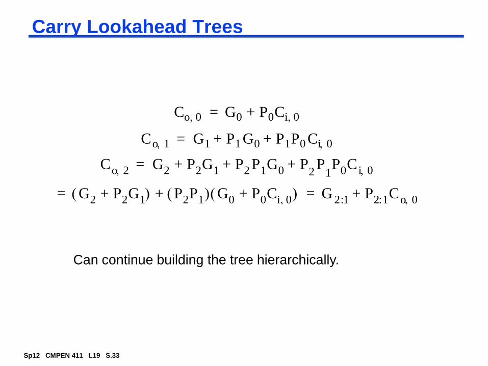
Sp12 CMPEN 411 L19 S.33
Carry Lookahead Trees
Co 0 G0 P0Ci 0+=
Co 1 G1 P1G0 P1P0Ci 0+ +=
Co 2 G2 P2G1 P2P1G0 P+2P
1P0C i 0+ +=
G2 P2G1+ = P2P1 G0 P0Ci 0+ + G2:1 P2:1Co 0+=
Can continue building the tree hierarchically.

Sp12 CMPEN 411 L19 S.34
Carry Operator
Define carry operator € on (G,P) signal pairs
€ is associative, i.e.,
[(g’’’,p’’’) € (g’’,p’’)] € (g’,p’) = (g’’’,p’’’) € [(g’’,p’’) € (g’,p’)]
€
(G’’,P’’) (G’,P’)
(G,P)
where
G = G’’ | P’’&G’
P = P’’&P’
€
€ €
€
G’
!G
G’’
P’’

Sp12 CMPEN 411 L19 S.35
PPA (Partially Prefix Adder) General Structure
Given P and G terms for each bit position, computing all the carries is equal to finding all the prefixes in parallel
(G0,P0) € (G1,P1) € (G2,P2) € … € (GN-2,PN-2) € (GN-1,PN-1)
Since € is associative, we can group them in any order
Measures to consider
number of € cells
tree cell depth (time)
tree cell area
cell fan-in and fan-out
max wiring length
wiring congestion
delay path variation (glitching)
Pi, Gi logic (1 unit delay)
Si logic (1 unit delay)
Ci parallel prefix logic tree
(1 unit delay per level)

Sp12 CMPEN 411 L19 S.36
Brent-Kung PPA
€
G0
P0
G1
P1
G2
p2
G3
P3
G4
P4
G5
P5
G6
P6
G7
P7
G8
P8
G9
p9
G10
P10
G11
p11
G12
P12
G13
p13
G14
p14
G15
p15
€€€€€€€
€ € € €
€
€
€
€
€
€
€ € € € € €
€ €
C1C2C3C4C5C6C7C8C9C10C11C12C13C14C15C16

Sp12 CMPEN 411 L19 S.37
A Faster Yet PPA
There are even faster PPA approaches that are used in most modern day machines for operands of 32 bits or greater
Kogge-Stone (KS)
faster pp tree (logN for KS versus 2logN-2 for BK)
fan-out of carry cell € limited to two
takes more € cells and has more wiring
Brent-Kung (BK) adder has the time bound of
TBK = 1 + (2log N – 2) + 1

Sp12 CMPEN 411 L19 S.38
Kogge-Stone PPF Adder
€
G0
P0
G1
P1
G2
P2
G3
P3
G4
P4
G5
P5
G6
P6
G7
P7
G8
P8
G9
P9
G10
P10
G11
P11
G12
P12
G13
P13
G14
P14
G15
P15
€€€€€€€
€ € € €
€
€
€
€
C1C2C3C4C5C6C7C8C9C10C11C12C13C14C15C16
Cin
€€€€€€€€
€ € € € € € € € € €
€ € € € € € € € € €
€ € € € € €
Tadd = tsetup + log2N t€ + tsum

Sp12 CMPEN 411 L19 S.39
PPA Comparisons
Measure BK PPA N=64 KS PPA N=64
# of € cells 2N - 2 - logN 129 NlogN - N + 1 321
tree depth 2logN - 2 10 logN 6
tree area (WxH)
(N/2) * (2logN -2) 320 N * logN 384
cell fan-in 2 2 2 2
cell fan-out logN 6 2 2
max wire length
N/4 16 N/2 32
wiring density
sparse dense
glitching high low

Sp12 CMPEN 411 L19 S.40
More Adder Comparisons
0
10
20
30
40
50
60
70
8 bits 16 bits 32 bits 48 bits 64 bits
RCA
CSkA
KS PPA

Sp12 CMPEN 411 L19 S.41
State of art

Sp12 CMPEN 411 L19 S.42
Next Lecture and Reminders
Next lecture
Multiplier Design
- Reading assignment – Rabaey, et al, 11.4