cmp users group 450mm technology development · process capability data progress 4 ... wet cleans 1...
TRANSCRIPT

CMP Users Group
450mm Technology Development
June 9, 2014
CNSE – RF / GLOBALFOUNDRIES / Intel / IBM / Samsung / TSMC

Key Messages
• Development Continues with all Suppliers
• Technical Results are Excellent with a Few Capabilities Identified as Challenges
• Wafer Supply
• Initial M1 grade wafers receive
• Notchless Wafer Standard being adjudicated
2 CNSE – RF / GLOBALFOUNDRIES / Intel / IBM / Samsung / TSMC

Development and Technology Intercept Targets
Early Development of Silicon and Infrastructure
G450C Program
ISMI 32/22nm Equipment Performance Metrics
Tools for Consortium Baseline, CIP and Demonstrations (unit process)
Early 450mm Development
Test Wafers to support development, improvement and demo
G450C Demonstrations 14nm
450mm and 300mm tools progress synchronously through technology generations
Full set (60+) of process and metrology tools and automation
10nm / 7nm
------ 2010 2011 2012 2013 2014 2015 2016 2016
Likely profile of tool work scope from delivery to finishing Baseline / CIP / Demo
3 CNSE – RF / GLOBALFOUNDRIES / Intel / IBM / Samsung / TSMC

Process Capability Data Progress
4
Total Process Application (PA) / Supplier combinations in Program Tools with data as of June MC
Tools meeting Program goal Tools projected to have data by year-end
PA / Supplier Combos 1 2 3 4 5 6 7 8 9 10 11 12 13 14 15 16 17 18 19 20 21 22
Functional Area
Wet Cleans1 PA / 1 Supplier; 1 PA / 2 Suppliers; 1 PA / 3 Suppliers
Dielectric Films5 PAs / 1 Supplier; 1 PA / 2 Suppliers; 5 PAs / 3 Suppliers
Metal Films5 PAs / 1 Supplier; 4 PAs / 2 Suppliers
Thermal3 PAs / 2 Suppliers; 1 PA / 3 Suppliers
Implant1 PA / 1 Supplier; 1 PA / 2 Suppliers
CMP3 PAs / 2 Suppliers
FEOL Etch2 PAs / 2 Supplier; 3 PAs / 3 Suppliers
BEOL Etch3 PAs / 3 Suppliers
Litho Track1 PA / 1 Supplier; 1 PA / 2 Suppliers
Defect Metrology2 PAs / 1 Supplier; 1 PA / 2 Suppliers
Films Metrology3 PAs / 1 Supplier
Litho Metrology1 PA / 1 Supplier; 2 PAs / 2 Suppliers

5
• SOKUDO DUO Track • Tool on schedule for 4Q2014 Albany, NY delivery
• Process capabilities include PT develop, NT develop, DSA coating, annealing, UV cure and wet etch
• SCREEN is providing 450mm wafer coating and DSA processing service from their Hikone facility
• Nikon 450mm 193i Scanner • First 193i scanner patterned 450mm wafers are
being presented at SEMICON West 2014
• 450mm patterning service being provided to G450C from the Nikon Kumagaya facility
• Nikon 450mm 193i scanner scheduled for delivery to the G450C in Albany, NY in April 2015
CNSE – RF / GLOBALFOUNDRIES / Intel / IBM / Samsung / TSMC
G450C Lithography Progress

Thermal/Cleans/CMP Summary
• Collected 1st M1 wafer sample (10 pcs) and a second source by Jun.
• Completed on-site F/BEOL wafer reclaim capability (Si, Ox, PR, SiN, Poly & TiN)
• Demonstrated 1st wafer result of 4 tools - SiN, a-Si, Flash, BEOL Cleans
• Passed 3 tools RFD (ready for development) and release to operation
- Scrubber, FEOL Clean and Anneal
• Complete 1st G450C EMA report of Oxide CMP
• Demonstrated defect performance of 1st Cu buffing CMP.
• Improved Si CMP reclaim defect result (Scratch reduction)
• Qualified 1st 450mm FOUP washer
6 CNSE – RF / GLOBALFOUNDRIES / Intel / IBM / Samsung / TSMC

Thermal/Cleans/CMP Process Application 450mm capability
THK, Non U%
(3 <2%; 2mm EE) Qty.
(wafers used)
Oxidation (Fur) Feb’ 14 / Jun’ 14 1116A, 1.3% / Jun’14 2000
SiN (Fur) Mar’14 / Feb’15 302A, 1.2%/ 15Q1 150
a-Si (Fur) Apr’14/ Feb’ 15 524A, 2.7% / 15Q2 140
RTP (SW) Jan’ 14/ Apr’ 14/ May’ 14
4.1% (3mm EE) / Rs, 6.6% (300mm) / Rs, 25%
26, 10 (300mm), 3
Oxide CMP Feb’ 13/ Jun’ 13 4.3% / 3.8% 100 / 300
W CMP Aug’ 14/ Jul’ 14 Aug’ 14/ Jul’ 14 0
Cu CMP Jul’ 14/ Feb’ 14 Jul’ 14/ 5.8% (5mm EE) 75
SiO2 wet etch Oct’13 3% 3
Application 450mm capability Adder defect, Size
(<20ea, 2mm EE, @>45nm)
Qty. (wafers used)
Scrubber (Backside) Sep’13 0 ea 5000
Particle Removal Oct’13/ Jun’ 14 -15 ea / Jul’14 7000
Post Ash strip Oct’13 10 ea 100
Solvent Clean Jun’14/ Jun’ 14/ 15Q2 -16 ea/ Jul’14 / 15Q2 1
Anneal (Fur) Dec’13/ Jun’ 14 3 ea / Jul’14 10
CNSE – RF / GLOBALFOUNDRIES / Intel / IBM / Samsung / TSMC

Thin-Film Status Update – by Application
Application ODD Current Status EPM Spec (10/7nm)
Ox/SiN
/SiCN
On site
On site
Aug’15
• Ox/SiN σ <1% (Released)
• Onsite tool : Tier 2 in progress.
• CIP in progress.
• U% 3σ <2.1% @1.5mm
• 1.6 < RI < 2.1
ULK
LK Cure
On site
Aug’15
Jun’14
• σ ~3.6 % (On site tool : Tier 2 in progress)
• Onsite tool: Tier 2 in progress
• 450mm structure wafer demo in progress.
• U% 3σ <2.1% @1.5mm EE
• Bulk K <2.6; 1.6<RI<2.1
FCVD Off site • σ ~9% 2.85% (without rotation)
• Demonstrated gap fill capability on coupon • U% 3σ <2.1% @1.5mm EE
a-C TBD • σ ~2.5 %
• Demonstrated no line collapsed post etch
• U% 3σ <2.1% @1.5mm EE
• Stress < 1GPa (Comp.)
ALD Ox On site
Jun’14 • No result yet. (Tool hook up in progress)
• U% 3σ <2.1% @1.5mm EE
• Step coverage >90%
ALD SiN/ SiOCN Off site • 8 wafers in measurement (G450C). • U% 3σ <2.1% @1.5mm EE
• Step coverage >90%
Epi Off site
• SiGe on poly σ ~8 %;
• Ready for SiGe deposition but w/I dopant until
Aug’14.
• U% 3σ <2.1% @1.5mm EE
• Ge%: 30%
PVD TaN/TiN/CuBS Off site
Q4’14
• σ <4%
• CIP in progress; Structure wafer demo in progress
• U% 3σ <2.1% @1.5mm EE
• Step coverage >80%
ALD TaN Off site • σ ~2.5 %
• Structure wafer demo in TEM check.
• U% 3σ <2.1% @1.5mm EE
• Step coverage >95%
FEOL Metal
(ALD TiAL, TiN, CVD
Co)
Q2’15 • No buildup yet. • U% 3σ <2.1% @1.5mm EE
• Step coverage > 95%
WCVD On site • σ ~8 %
• Tool Hook up in progress. (E/May)
• U% 3σ <2.1% @1.5mm EE
• Void free
Cu-plating On site
Dec’15
• σ <3 %
• Tier 2 qualification in progress. (May’14)
• U% 3σ <2.1% @1.5mm EE
• Void free
Ion Implant Jul’14
Off site
• σ <1 %
• U% 3σ <2.1% @1.5mm EE
• Beam stability +/- 1%

G450C On-site Wafer reclaim ready (Si/ Ox/ PR/ SiN/ Poly/ TiN)
Process Film
2013 4Q 2014 1Q 2014 2Q 2014 3Q
10 11 12 1 2 3 4 5 6 7 8 9
FEOL Si/Oxide / SiN / PR ★
Poly ★
BEOL Metal (TiN) ★
Wafer Reclaim Capability
★ G450C On-site ready
9
Poly Removal
Poly/Oxide Wafer Reclaim
Thic
kne
ss (
A)
TiN Removal
TiN/Oxide Wafer Reclaim
Thic
knes
s (A
)
CNSE – RF / GLOBALFOUNDRIES / Intel / IBM / Samsung / TSMC

KT (SP3) Particle Area Scratch(mm) Grade B < 250 <5mm2 0 Grade C < 500 <5mm2 <5 Grade D < 1000 <5mm2 <10 Grade E > 2000 >30mm2 >10
CMP Update
Pre (w/scratch)
Grade E
Tool / Process
10
CMP + on-site CLN
Grade C
~1.5um Si loss
Pre-CMP Post-CMP
467ea@45nm [email protected] 26 [email protected] ~50mm scratch
Spec: < [email protected]
CNSE – RF / GLOBALFOUNDRIES / Intel / IBM / Samsung / TSMC

Wafer Quality Roadmap
Wafer quality roadmap
Collected 1st M1 wafer sample (10 pcs)
4 pcs suffered local scratch issue, still under investigation.
M74 Spec
M76 Spec
2012 2013 2014 2015 2016
1H 2H 1H 2H 1H 2H 1H 2H 1H 2H
M62 Spec
M1 Spec
Q2, 2014
Q1, 2015
Deliver Sample
Mechanical Wafer
Test/Monitor Wafer
Prime Wafer
EPI Wafer
*SFQR: Site Flatness Quality Requirement (<20nm)
Wafer Type
14Q4: 1st 450mm EPI reactor
SFQR meet (~95% area)
Particle (60% pass rate)
11 CNSE – RF / GLOBALFOUNDRIES / Intel / IBM / Samsung / TSMC
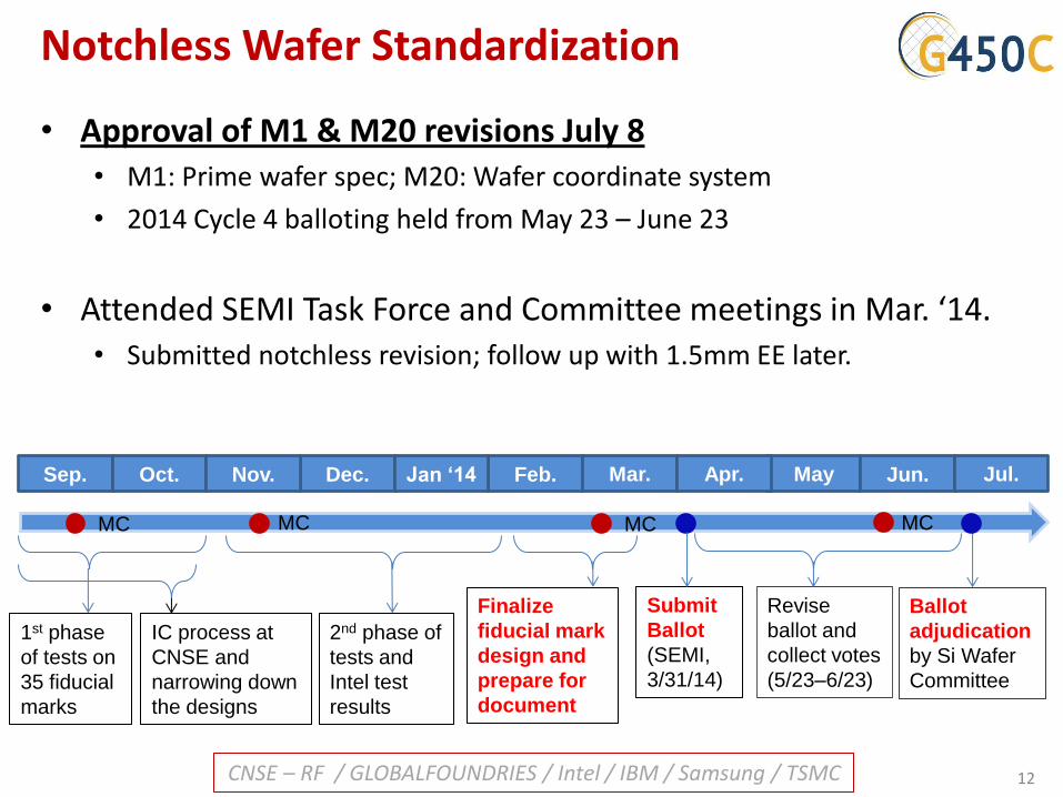
Notchless Wafer Standardization
• Approval of M1 & M20 revisions July 8 • M1: Prime wafer spec; M20: Wafer coordinate system
• 2014 Cycle 4 balloting held from May 23 – June 23
• Attended SEMI Task Force and Committee meetings in Mar. ‘14. • Submitted notchless revision; follow up with 1.5mm EE later.
May
1st phase
of tests on
35 fiducial
marks
Submit
Ballot
(SEMI,
3/31/14)
2nd phase of
tests and
Intel test
results
IC process at
CNSE and
narrowing down
the designs
Ballot
adjudication
by Si Wafer
Committee
Finalize
fiducial mark
design and
prepare for
document
Jun. Sep. Oct. Feb. Dec. Nov. Mar. Apr. Jul. Jan ‘14
MC MC MC
Revise
ballot and
collect votes
(5/23–6/23)
MC
12 CNSE – RF / GLOBALFOUNDRIES / Intel / IBM / Samsung / TSMC

G450C Metrology Status
Tool Type Application Status Future plan
SE/OCD Dielectric/thin metal film thickness Stress Pattern OCD
Thickness -operational OCD – Q3 2016
OCD monitor for <28nm
4P Probe Sheet resistance Operational
3DAFM Nanotopography Pattern CD bigger than 40nm pitch
Operational Tip development for <28nm pitch 3D measurement
TXRF Metallic contamination Operational VPD integrated tool under negotiation
XRR/XRF Opaque film thickness, density Operational
Overlay Overlay Diffraction Based Overlay
AMC Analyzer Outgassing of wafers and carriers, FOUP clean qual
To be on-site Q3 2014
CD-SEM ADI / AEI pattern CD Off-site Q3-Q4 2014, On-site Q1 2015
Advanced Wafer Geometry
SFQR,ERO, GBIR, nanotopography
13 CNSE – RF / GLOBALFOUNDRIES / Intel / IBM / Samsung / TSMC Confidential

G450C Inspection Tool Status
Tool Type Application Status Future plan
Macro Inspection Macro defect inspection - blanket/patterned - front/backside/bevel (EBR)
Operational
Defect Review SEM Defect imaging with EDS analysis Pattern CD measurement
Operational
Bare Particle Non patterned wafer particle 2 tools operational edge grip development 22nm capability
BF Inspection Patterned wafer inspection To be available Q1 2015, off-sight
DF Inspection Patterned wafer inspection To be available Q1 2016 Off-site
Edge Inspection Edge defect inspection Edge metrology
Available Q3 2014 Bevel etch equipment evaluation
Ebeam Inspection Patterned wafer inspection Surveying
14 CNSE – RF / GLOBALFOUNDRIES / Intel / IBM / Samsung / TSMC
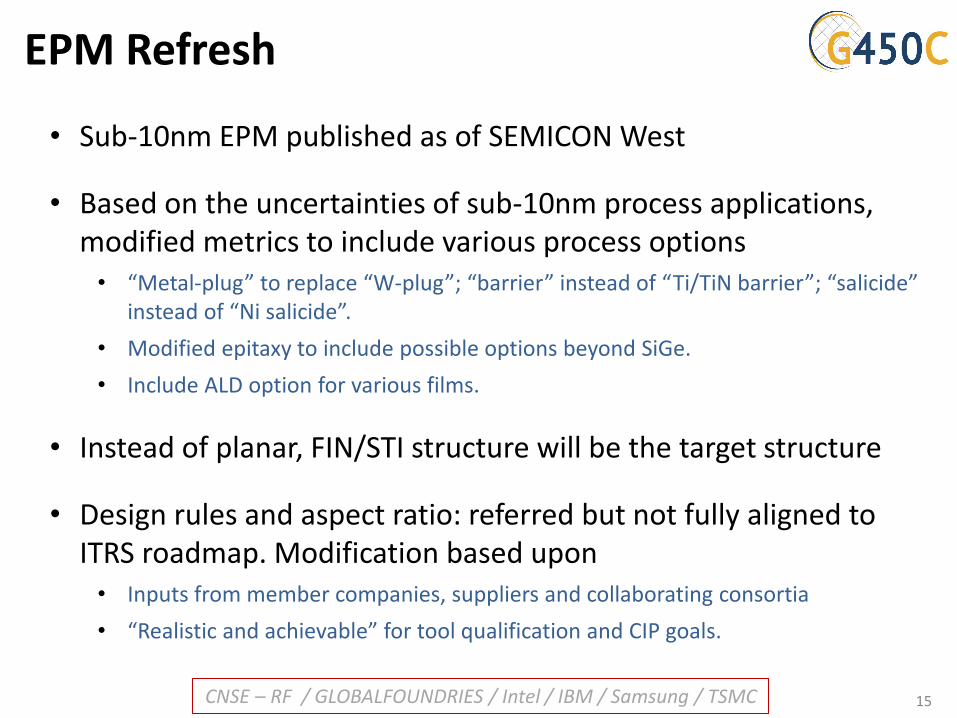
• Sub-10nm EPM published as of SEMICON West
• Based on the uncertainties of sub-10nm process applications, modified metrics to include various process options
• “Metal-plug” to replace “W-plug”; “barrier” instead of “Ti/TiN barrier”; “salicide” instead of “Ni salicide”.
• Modified epitaxy to include possible options beyond SiGe.
• Include ALD option for various films.
• Instead of planar, FIN/STI structure will be the target structure
• Design rules and aspect ratio: referred but not fully aligned to ITRS roadmap. Modification based upon
• Inputs from member companies, suppliers and collaborating consortia
• “Realistic and achievable” for tool qualification and CIP goals.
EPM Refresh
15 CNSE – RF / GLOBALFOUNDRIES / Intel / IBM / Samsung / TSMC

Items 14nm < 10nm Scaled DTM
Module
FIN/STI Full Pitch 42nm (Fin 10nm) 24nm (Fin 8nm) 28nm (Fin 8nm)
Contact CD 20nm (AR 10:1) 10nm (AR 10:1) 10nm (AR 10:1)
Poly Full Pitch* 42nm (Line AR 5:1) 24nm (Line AR 5:1) 28nm (Line AR 5:1)
BEOL Trench Full Pitch 54nm (Trench AR 3:1) 26nm (Trench AR 3:1) 28nm (Trench AR 3:1)
Generic Items
PWP Particle Size > 30nm > 21nm > 22nm
PWP Backside Particle 50nm 50nm
Basic Total Variability* < 3.0% < 2.1%
Basic Target Thickness 100% 70%
Basic Geometry to meet pitch shrink 100 50
*Total Variability 𝑇𝑉 = 𝐼𝑊𝑈2 + 𝑊𝑇𝑊2 + 𝐿𝑇𝐿2
• Targeted Device Dimension and Basic Generic Rules
EPM Revision Generic Rules
16 CNSE – RF / GLOBALFOUNDRIES / Intel / IBM / Samsung / TSMC

450mm Tool Demonstrations
• Milestones
• EMA report
• Baseline Characterization report
• Final Demo report
• Focus on current supplier readiness/data in 2014, focus CIP sub-10nm for 2015-2016
17 CNSE – RF / GLOBALFOUNDRIES / Intel / IBM / Samsung / TSMC

SA/Marathon
Sub-10nm Collaborative Development & Equipment Demonstrations
EMA
Sub-10nm Collaborative Development
Maturity Info/Capability Data Baseline
Agreement On Scaled
Targets
Data Info Data
Info Data
Data
Info
Data
Demo Ready?
18 CNSE – RF / GLOBALFOUNDRIES / Intel / IBM / Samsung / TSMC

G450C Coordination
• EEMI450 feedback (including IMEC and Suppliers) improved multiple parameters in sub-10nm Equipment Performance Metrics
• Joint planning on demos at G450C and IMEC: standard methods / data exchange • Working with Metro450 to address slip measurement • Planning contamination analysis by Fraunhofer and TNO
• Discussions on CMP slurry recycling with Silicon Saxony companies: characterize capability and reduce water use
• Working with ESG-J on SEMI Carrier Standards refinement
• Ongoing facilities / EHS work with F450C • Component Lift Guidelines • Pump/Abatement Green Mode • Utilities use rates, effluents / PFC emissions • He recycling & Airborne Molecular Contamination
19 CNSE – RF / GLOBALFOUNDRIES / Intel / IBM / Samsung / TSMC

Summary
• 450mm Technical Results are Excellent
• Full 193i Patterning Capability Demonstrated
• Notchless Wafer Standard Approved
• CMP for High Aspect Ratio a Critical Challenge for 450mm
CNSE – RF / GLOBALFOUNDRIES / Intel / IBM / Samsung / TSMC 20

Questions and Answers
300mm & 450mm wafers
21
450mm 193i patterned wafer
CNSE – RF / GLOBALFOUNDRIES / Intel / IBM / Samsung / TSMC