cmos technology nodes: trends, challenges, opportunities?
TRANSCRIPT

IBM Research – T. J. Watson Research Center
CMOS Technology Nodes:CMOS Technology Nodes:Trends,Trends,Challenges,Challenges,Opportunities?Opportunities?
Ghavam Shahidi
IBM Research Division
2
IBM Research
CMOS Scaling: CMOS Scaling: DennardDennard’’ss Theory Theory
Smaller
Faster
Lower Power
Scaled technology generations

3
IBM Research
Device Performance: ~30% per GenerationDevice Performance: ~30% per Generation
4
IBM Research
Performance ChallengePerformance Challenge
Technology performance gain continuing
– Through 32-22 nm nodes
– Power-delay curve improving
Issue: Supply voltage not going down
– Power density (and power)
Solution: Industry moving to multi “low-power” cores
– Performance not through frequency
Do we care as much about performance?
– System performance: Number of cores vs. the frequency
Drive to higher VT’s and lower supply => Effectively devices not as fast

5
IBM Research
CMOS Density: MooreCMOS Density: Moore’’s Laws Law
30% Reduction in W and device pitch
– 50% area reduction
– 2X device/area (every 2 years)
Devic
e P
itch
W
6
IBM Research
Device Pitch ScalingDevice Pitch Scaling
2006230-35065
55-65
70-80
90-100
120-130
170-180
Device Pitch (nm)
2017-18
2014-15
2012
2010
2008
Year
15
22
11
32
45
Node
7
IBM Research
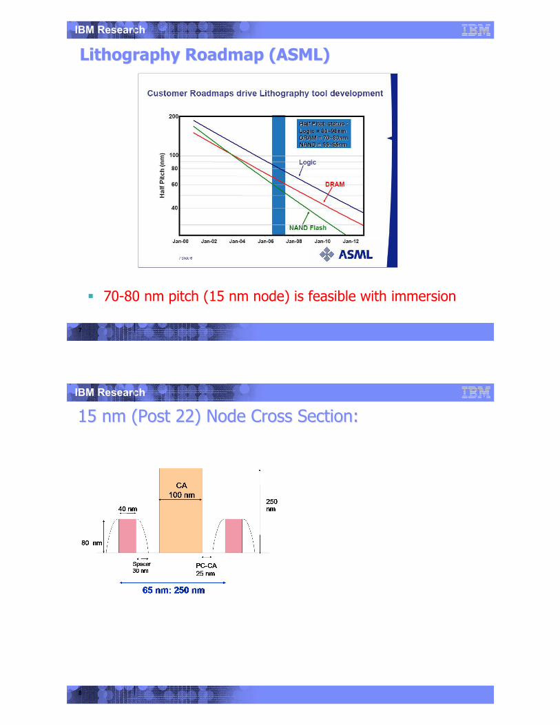
Lithography Roadmap (ASML)Lithography Roadmap (ASML)
70-80 nm pitch (15 nm node) is feasible with immersion
8
IBM Research
15 nm (Post 22) Node Cross Section:15 nm (Post 22) Node Cross Section:

9
IBM Research
15 nm (Post 22) Node Cross Section:15 nm (Post 22) Node Cross Section:
10
IBM Research
15 nm (Post 22) Node Cross Section:15 nm (Post 22) Node Cross Section:

11
IBM Research
Challenge: L ScalingChallenge: L Scaling
30
40
50
60
70
80
90
180n
m13
0nm
90nm
65nm
45nm
32nm
*
22nm
*
Technology
Gate
Length
(nm
)
12
IBM Research
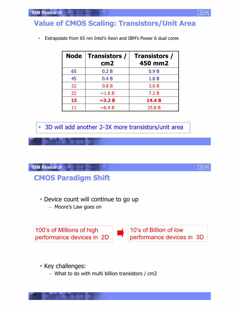
Value of CMOS Scaling: Transistors/Unit AreaValue of CMOS Scaling: Transistors/Unit Area
0.9 B0.2 B65
~6.4 B
~3.2 B
~1.6 B
0.8 B
0.4 B
Transistors /cm2
25.8 B
14.4 B
7.2 B
3.6 B
1.8 B
Transistors /450 mm2
15
22
11
32
45
Node
Extrapolate from 65 nm Intel’s Xeon and IBM’s Power 6 dual cores
13
IBM Research
Value of CMOS Scaling: Transistors/Unit AreaValue of CMOS Scaling: Transistors/Unit Area
0.9 B0.2 B65
~6.4 B
~3.2 B
~1.6 B
0.8 B
0.4 B
Transistors /cm2
25.8 B
14.4 B
7.2 B
3.6 B
1.8 B
Transistors /450 mm2
15
22
11
32
45
Node
Extrapolate from 65 nm Intel’s Xeon and IBM’s Power 6 dual cores
3D will add another 2-3X more transistors/unit area
14
IBM Research
CMOS Paradigm ShiftCMOS Paradigm Shift
Device count will continue to go up– Moore’s Law goes on
Key challenges:– What to do with multi billion transistors / cm2
100’s of Millions of high
performance devices in 2D
10’s of Billion of low
performance devices in 3D
15
IBM Research
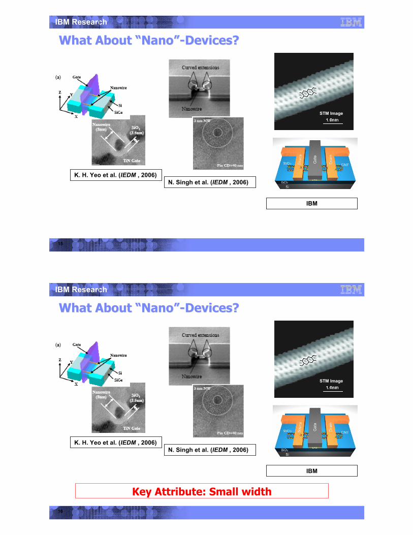
What About What About ““NanoNano””-Devices?-Devices?
K. H. Yeo et al. (IEDM , 2006)
N. Singh et al. (IEDM , 2006)
STM Image
IBM
16
IBM Research
What About What About ““NanoNano””-Devices?-Devices?
K. H. Yeo et al. (IEDM , 2006)
N. Singh et al. (IEDM , 2006)
STM Image
IBM
Key Attribute: Small width

17
IBM Research
When Will We Get to Real When Will We Get to Real NanoNano??
10-168
7-105
16-2511
25-35
35-45
50-60
70-80
Minimum W (nm)
15
22
32
45
Node
Nano-devices by 2020-2025 in production?
Key Attribute: Small width