cmos mobility-compensated time reference for crystal
TRANSCRIPT
UNIVERSIDADE FEDERAL DE SANTA CATARINAENGENHARIA ELETRICA
Agossou Wilfried Zomagboguelou
CMOS MOBILITY-COMPENSATED TIME REFERENCE FORCRYSTAL REPLACEMENT
Florianopolis
2015

Agossou Wilfried Zomagboguelou
CMOS MOBILITY-COMPENSATED TIME REFERENCE FORCRYSTAL REPLACEMENT
Dissertacao submetida ao Programa de Pos-graduacao em engenharia eletrica da Universidade Federal de Santa Catarina para a obtenção do grau de Mestre em engenharia Elétrica .Advisor: Prof. Dr. Marcio Cherem Schnei-der
Florianopolis
2015

Ficha de identificação da obra elaborada pelo autor, através do Programa de Geração Automática da Biblioteca Universitária da UFSC.
Zomagboguelou, Agossou Wilfried CMOS MOBILITY-COMPENSATED TIME REFERENCE FOR CRYSTALREPLACEMENT / Agossou Wilfried Zomagboguelou ; orientador,Marcio Cherem Schneider - Florianópolis, SC, 2015. p.
Dissertação (mestrado) - Universidade Federal de SantaCatarina, Centro Tecnológico. Programa de Pós-Graduação emEngenharia Elétrica.
Inclui referências
1. Engenharia Elétrica. 2. Relaxation Oscillatorindependent with Process, Voltage and Temeperature. 3.Time reference . 4. Zero-Vt MOSFET as resistor. 5. Currentmode Schmitt trigger. I. Cherem Schneider, Marcio . II.Universidade Federal de Santa Catarina. Programa de PósGraduação em Engenharia Elétrica. III. Título.

Agossou Wilfried Zomagboguelou
CMOS MOBILITY-COMPENSATED TIME REFERENCE FORCRYSTAL REPLACEMENT
Esta Dissertacao foi julgada aprovada para a obtencao do Tıtulo de“Mestre”, e aprovada em sua forma final pelo Programa de Pos-graduacaoem engenharia eletrica.
Florianopolis, 30 de November 2015.
Prof. Dr. Carlos Galup-MontoroCoordenador
Universidade Federal de Santa Catarina
Banca Examinadora:
Carlos Galup-Montoro, DrUniversidade Federal de Santa Catarina.
Hector Pettenghi Roldan, DrUniversidade Federal de Santa Catarina
Marcio Bender Machado, DrIF-Sul Pelotas
Paulo Augusto Dal Fabbro, DrChipus


Ce Master thesis est dedie a mon frere Victo-rien Zomagboguelou.

ACKNOWLEDGEMENTS
Firstly, I would like to express my sincere gratitude to my advisor Prof.Marcio Schneider for the continuous support of my master degree study andrelated research, for his patience, motivation, and immense knowledge. Hisguidance helped me in all the time of research and writing of this master the-sis. And also my sincere gratitude to Prof. Carlos Galup for the opportunitygiven to join LCI (Laboratorio de Circuito Integrado) and his mentoring inthis master thesis. I could not have imagined having a better advisor and men-tor for my master degree study. And my sincere thanks to CNPQ ConselhoNacional de Desenvolvimento Cientıfico e Tecnologico for the scholarship,and to MOSIS for fabricate my circuit through multi-project wafers (MPW).
My sincere thanks also go to Prof. Adroaldo Raizer, who gave accessto the research facilities (MagLab-UFSC), and Dr. Arun Kumar Sinha, forthe discussions about analog environment tool and support. I feel that withouttheir precious support, it would not be possible to conduct this research work.
I would also like to thank Luiz Alberto Pasini Melek, and Dr. MarcioBender for their advise in layout design and submitting design to the MOSIS.Also I would like to thanks, Ms. Nazide and to all the students working inLCI with their name listed as: Mr. Daniel Novak, Mr. Yuri, Mr. Anselmo,Mr. Fernando and Mr. Jefferson.

RESUMO
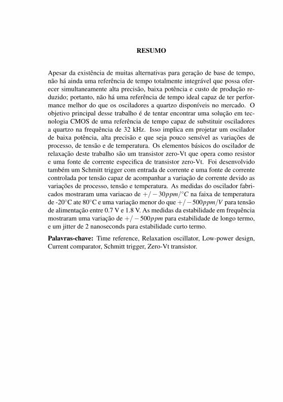
Apesar da existencia de muitas alternativas para geracao de base de tempo,nao ha ainda uma referencia de tempo totalmente integravel que possa ofer-ecer simultaneamente alta precisao, baixa potencia e custo de producao re-duzido; portanto, nao ha uma referencia de tempo ideal capaz de ter perfor-mance melhor do que os osciladores a quartzo disponıveis no mercado. Oobjetivo principal desse trabalho e de tentar encontrar uma solucao em tec-nologia CMOS de uma referencia de tempo capaz de substituir osciladoresa quartzo na frequencia de 32 kHz. Isso implica em projetar um osciladorde baixa potencia, alta precisao e que seja pouco sensıvel as variacoes deprocesso, de tensao e de temperatura. Os elementos basicos do oscilador derelaxacao deste trabalho sao um transistor zero-Vt que opera como resistore uma fonte de corrente especifica de transistor zero-Vt. Foi desenvolvidotambem um Schmitt trigger com entrada de corrente e uma fonte de correntecontrolada por tensao capaz de acompanhar a variacao de corrente devido asvariacoes de processo, tensao e temperatura. As medidas do oscilador fabri-cados mostraram uma variacao de +/− 30ppm/◦C na faixa de temperaturade -20◦C ate 80◦C e uma variacao menor do que +/−500ppm/V para tensaode alimentacao entre 0.7 V e 1.8 V. As medidas da estabilidade em frequenciamostraram uma variacao de +/−500ppm para estabilidade de longo termo,e um jitter de 2 nanoseconds para estabilidade curto termo.
Palavras-chave: Time reference, Relaxation oscillator, Low-power design,Current comparator, Schmitt trigger, Zero-Vt transistor.


ABSTRACT
Despite many alternatives for time generation, no CMOS fully-integratedtime reference offers simultaneously high accuracy, low power consumption,and low cost, and, thus, no ideal time reference suitable to replace the xtal-clock is available. The main aim of this work is to contribute to find a solu-tion to this problem, which is to realize a low-cost, low-power CMOS timereference circuit that is insensitive to PVT (Process, Voltage, and Tempera-ture) variations. The basic element of the relaxation oscillator is a zero-VtMOSFET that operates as a resistor and a current source which tracks thespecific current of the zero-Vt transistor. The design presented here uses acurrent mode Schmitt trigger and a voltage controlled current source, whichcan track the current variation due to PVT variations. The frequency of os-cillation, proportional to the mobility, is compensated by the thermal voltage.The proposed time reference, fabricated in a 180 nm CMOS technology hasbeen designed for 32 kHz. Test and measurement results show a variation of+/− 30ppm/◦C from -20◦C to 80◦C, and less than +/− 500ppm/V for avariation of the supply voltage between 0.7 V to 1.8 V. As regards frequencystability, measurements have shown a variation less than +/− 500ppm forlong term stability, and an rms jitter of 2 nanoseconds (66 ppm) for shortterm stability.
Keywords: Time reference, Relaxation oscillator, Low-power design, Cur-rent comparator, Schmitt trigger, Zero-Vt transistor.

CONTENTS
1 INTRODUCTION . . . . . . . . . . . . . . . . . . . . . . . . . . . . . . . . . . . . . 151.1 MOTIVATION . . . . . . . . . . . . . . . . . . . . . . . . . . . . . . . . . . . . . . . . . 151.2 CRYSTAL OSCILLATOR . . . . . . . . . . . . . . . . . . . . . . . . . . . . . . . 171.3 PHYSICAL AND ELECTRICAL FACTORS AFFECTING CRYS-
TAL OSCILLATOR FREQUENCY STABILITY AND AC-CURACY . . . . . . . . . . . . . . . . . . . . . . . . . . . . . . . . . . . . . . . . . . . . . 19
1.4 AVAILABLE TECHNIQUES TO REPLACE XTAL-OSCILLATORS 211.4.1 MEMS oscillator . . . . . . . . . . . . . . . . . . . . . . . . . . . . . . . . . . . . . . 211.4.2 LC oscillator . . . . . . . . . . . . . . . . . . . . . . . . . . . . . . . . . . . . . . . . . . 221.4.3 Relaxation oscillator with positive feedback . . . . . . . . . . . . . . 231.4.4 Relaxation oscillator using comparators . . . . . . . . . . . . . . . . . 261.4.5 Mobility-based relaxation oscillator . . . . . . . . . . . . . . . . . . . . . 271.5 MOBILITY IN MOSFETS . . . . . . . . . . . . . . . . . . . . . . . . . . . . . . 291.5.1 Some theory on mobility with temperature variation . . . . . . 301.5.2 Coulomb mobility µcoulomb . . . . . . . . . . . . . . . . . . . . . . . . . . . . . . 311.5.3 Acoustic phonon mobility µac . . . . . . . . . . . . . . . . . . . . . . . . . . . 311.5.4 Surface roughness mobility µsr . . . . . . . . . . . . . . . . . . . . . . . . . . 311.5.5 Bulk mobility µb . . . . . . . . . . . . . . . . . . . . . . . . . . . . . . . . . . . . . . 321.5.6 Simulation of mobility with respect to temperature variation 321.6 COMPARISON BETWEEN TECHNIQUES AVAILABLE TO
GENERATE TIME REFERENCES . . . . . . . . . . . . . . . . . . . . . . . 351.7 PROPOSED MOBILITY-COMPENSATED TIME REFERENCE 372 ZERO-VT SELF-BIASED CURRENT SOURCE (SBCS) . . 392.1 SELF-BIASED CURRENT SOURCE (SBCS) DESIGN. . . . . . 392.2 ZERO-VT SELF-BIASED CURRENT SOURCE . . . . . . . . . . . 422.2.1 Proposed zero-Vt self-biased current source . . . . . . . . . . . . . . 422.2.2 Simulation result of the zero-Vt Self-Biased current source . 443 VOLTAGE-CONTROLLED CURRENT SOURCE . . . . . . . 473.1 OPERATIONAL TRANSCONDUCTANCE AMPLIFIER DE-
SIGN . . . . . . . . . . . . . . . . . . . . . . . . . . . . . . . . . . . . . . . . . . . . . . . . . 473.2 COMMON SOURCE AMPLIFIER WITH ACTIVE LOAD . . . 483.3 VOLTAGE CONTROLLED CURRENT SOURCE . . . . . . . . . . 503.3.0.1 Comments on the nonlinear characteristic of the MOSFET . . . . 524 CURRENT MODE SCHMITT TRIGGER (CMST) . . . . . . . 554.1 STATE-OF-THE-ART OF CURRENT COMPARATORS . . . . 554.2 PROPOSED CURRENT-MODE SCHMITT TRIGGER (CMST) 594.2.1 Current comparator . . . . . . . . . . . . . . . . . . . . . . . . . . . . . . . . . . 59

4.2.1.1 Current difference stage . . . . . . . . . . . . . . . . . . . . . . . . . . . . . . . . . 604.2.1.2 Proposed gain stage . . . . . . . . . . . . . . . . . . . . . . . . . . . . . . . . . . . . . 604.2.1.3 Output stage . . . . . . . . . . . . . . . . . . . . . . . . . . . . . . . . . . . . . . . . . . . 624.2.2 Current mode Schmitt trigger . . . . . . . . . . . . . . . . . . . . . . . . . . 634.3 HIGH SWING CURRENT MIRROR . . . . . . . . . . . . . . . . . . . . . . 665 MOBILITY-COMPENSATED TIME REFERENCE . . . . . . 695.1 PRINCIPLE OF THE MOBILITY-COMPENSATED TIME REF-
ERENCE . . . . . . . . . . . . . . . . . . . . . . . . . . . . . . . . . . . . . . . . . . . . . 695.1.1 The MOSFET as a capacitor . . . . . . . . . . . . . . . . . . . . . . . . . . . . 735.2 MATHEMATICAL MODEL OF THE PROPOSED MOBILITY-
COMPENSATED TIME REFERENCE . . . . . . . . . . . . . . . . . . . . 745.3 SIMULATION RESULTS . . . . . . . . . . . . . . . . . . . . . . . . . . . . . . . 765.4 TEST AND MEASUREMENT RESULTS . . . . . . . . . . . . . . . . . 775.4.1 Variation of oscillation frequency with supply voltage . . . . . 825.4.2 Temperature variation . . . . . . . . . . . . . . . . . . . . . . . . . . . . . . . . . 845.4.3 Short term noise analysis . . . . . . . . . . . . . . . . . . . . . . . . . . . . . . . 855.4.4 Long term analysis . . . . . . . . . . . . . . . . . . . . . . . . . . . . . . . . . . . . 866 CONCLUSION . . . . . . . . . . . . . . . . . . . . . . . . . . . . . . . . . . . . . . . 896.1 MAIN RESULT . . . . . . . . . . . . . . . . . . . . . . . . . . . . . . . . . . . . . . . . 896.2 FUTURE WORK . . . . . . . . . . . . . . . . . . . . . . . . . . . . . . . . . . . . . . 89
APPENDIX A -- Advanced Compact Model . . . . . . . . . . . . . . 93APPENDIX B -- Figure of Merit of the oscillator as timereference . . . . . . . . . . . . . . . . . . . . . . . . . . . . . . . . . . . . . . . . . . . . . 97
List of Figures . . . . . . . . . . . . . . . . . . . . . . . . . . . . . . . . . . . . . . . . . . . . . . . 101List of Tables . . . . . . . . . . . . . . . . . . . . . . . . . . . . . . . . . . . . . . . . . . . . . . . . 105
Bibliography . . . . . . . . . . . . . . . . . . . . . . . . . . . . . . . . . . . . . . . . . . 107

15
1 INTRODUCTION
Many services running on modern digital telecommunications net-works require accurate synchronization for correct operation [1], [2]. Forexample, if switches do not operate with the same clock rates, then slips willoccur and will degrade performance. Also telecommunications networks relyon the use of highly accurate primary reference clocks, which are distributedover wide networks using synchronization links and synchronization supplyunits. Time reference is also used as a clock in watch when the time is pre-cise and stable or in RF sleep mode in cellular [3] as shown in Fig.1, whenthe time reference is stable and consume low power.
Figure 1 – Example of use of xtal oscillator in cell phone [3]
In this work we will present methods used to generate a time reference.We will design a time reference in CMOS technology that can be suitable toreplace the most common time reference i.e., the crystal oscillator, in someapplications where only stability and precision are required.
1.1 MOTIVATION
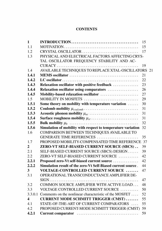
In the beginning of 1968 the concept of integrated time reference wereexplored [4], when oscillators of type ”Wien-bridge” as the one shown inFig. 2 were presented.
16
Figure 2 – Wien Bridge Oscillator [4]
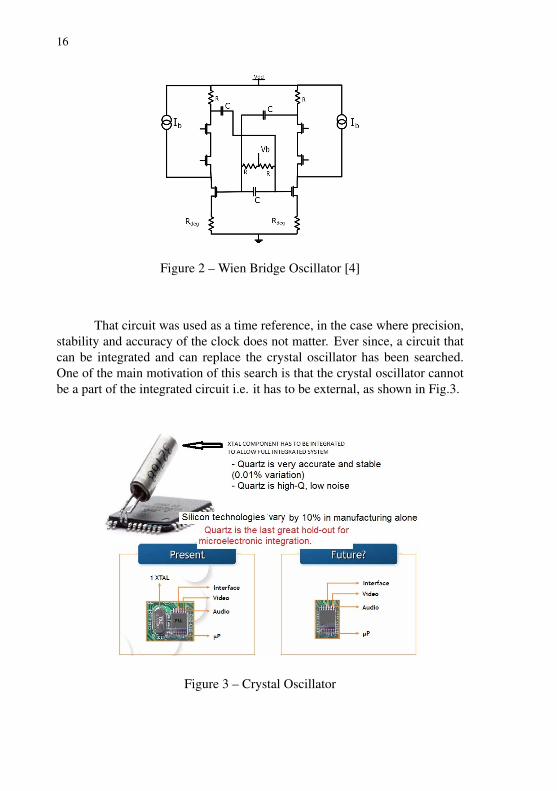
That circuit was used as a time reference, in the case where precision,stability and accuracy of the clock does not matter. Ever since, a circuit thatcan be integrated and can replace the crystal oscillator has been searched.One of the main motivation of this search is that the crystal oscillator cannotbe a part of the integrated circuit i.e. it has to be external, as shown in Fig.3.
Figure 3 – Crystal Oscillator

17
1.2 CRYSTAL OSCILLATOR
The crystal resonator is the most important component of a crystaloscillator and the quartz crystal is the heart of it. A quartz crystal is ananisotropic crystal of silicon dioxide. The crystal structure consists of twopyramidal ends and is hexagonal in cross-section. Fig. 4 illustrates the physi-cal structure of a quartz crystal.
Figure 4 – Cuts of the crystal resonator [5]
Figure 5 – Equivalent circuit of the crystal oscillator [6]
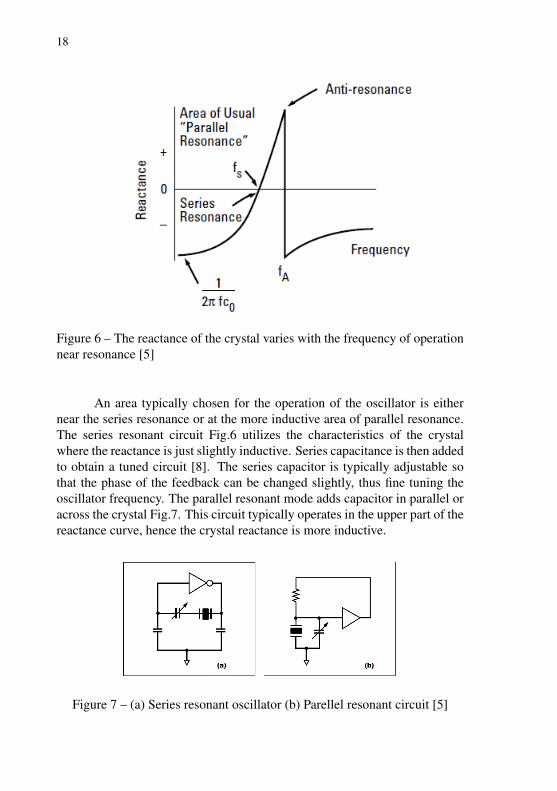
The equivalent circuit of the crystal oscillator, shown in Fig.5, pro-vides the link between the physical property of the crystal and the area ofapplication, the oscillator [7]. The physical constants of the crystal determinethe equivalent values of R1, C1, L1, and C0. R1 is a result of bulk losses, C1,the motional capacitance, L1 is determined by the mass, and C0 is made up ofthe electrodes, and the leads [8]. When operated far off resonance, the struc-ture is simply a capacitor C0 but, at the precise resonant frequency the circuitbecomes a capacitor and resistor in parallel, as shown in Fig.6. The reactanceof the crystal approaches zero at the point of series resonance [8], and reachesa maximum at the anti-resonant frequency fA, as Fig.6 shows.
18
Figure 6 – The reactance of the crystal varies with the frequency of operationnear resonance [5]
An area typically chosen for the operation of the oscillator is eithernear the series resonance or at the more inductive area of parallel resonance.The series resonant circuit Fig.6 utilizes the characteristics of the crystalwhere the reactance is just slightly inductive. Series capacitance is then addedto obtain a tuned circuit [8]. The series capacitor is typically adjustable sothat the phase of the feedback can be changed slightly, thus fine tuning theoscillator frequency. The parallel resonant mode adds capacitor in parallel oracross the crystal Fig.7. This circuit typically operates in the upper part of thereactance curve, hence the crystal reactance is more inductive.
Figure 7 – (a) Series resonant oscillator (b) Parellel resonant circuit [5]

19
1.3 PHYSICAL AND ELECTRICAL FACTORS AFFECTING CRYSTALOSCILLATOR FREQUENCY STABILITY AND ACCURACY
A small piece of quartz material is obtained by cutting the crystal atspecific angles to the various axes. The choice of axis and angles determinethe physical and electrical parameters of the resonator. The frequency, or rateof vibration, is determined by the cut, size, and shape of the resonator.
• TemperatureTemperature is a significant factor which affects the frequency of res-onators. Different crystal cuts have a different frequency-temperaturecharacteristic as shown in Fig. 8. AT, XY, DT, CT, and BT representdifferent crystal cut methods. The primary frequency determining fac-tor for the AT, XY, DT, CT, and BT cut is thickness since they vibratein the thickness shear mode. The precision with which the thickness iscontrolled determines the frequency variation from crystal to crystal.
Figure 8 – Crystal with temperature variation at different fabrication process[5]

20
Figure 9 – Aging of crystal resonator over time [6]
• AgingThe crystal resonator frequency will change according to the operationtime. This physical phenomenon is termed as aging. It should be notedthat although the plot in Fig.9 is monotonic, this is not always the caseand the aging rate can reverse sign over time.
• Drive LevelIn a precise crystal resonator, the oscillator frequency also relies on thecrystal electric current or drive level. The equation is:
δ ff
= k.i2 (1.1)
Here, ”i” is the alternating-current which flows through the crystal, kis a constant which is dependent on the crystal, and δ f
f is the relativevariation of the vibration frequency. When the drive electric currentis high, the aging property and long-term frequency stability will beworse. But when the drive level is too small, the noise electric current
21
may be relatively high compared to the crystal electric current, and thiswill cause the worse short-term frequency stability.
• RetraceWhen power is removed from an oscillator for several hours, then re-applied on it again, the frequency of this oscillator will stabilize at aslightly different value. This frequency variation error is called retraceerror. It usually occurs for twenty four or more hours off-time followedby a warm-up time which is enough to complete thermal equilibrium.
• Power supply noiseThe power supply noise is one of the sources of oscillator phase noise;especially, for ring-based voltage-controlled oscillators, it is the dom-inant noise source. Such noise typically appears as steps or impulseson the power supply of the oscillator, and it affects both frequency andphase, causing cycle-to-cycle jitter.
1.4 AVAILABLE TECHNIQUES TO REPLACE XTAL-OSCILLATORS
1.4.1 MEMS oscillator
Quartz crystal resonators are excited at their resonance frequency byan electrical oscillator circuit [9],[10],[11]. Their operation depends on thepiezoelectric properties of a material that cannot be integrated in IC technol-ogy. Over the years, a lot of research has been done on the development ofsilicon MEMS-based (Micro Electro-Mechanical Systems-based) resonatorswith the aim of replacing quartz crystals. MEMS technology involves manyof the processes used by the integrated circuit technology such as lithogra-phy, deposition, etching, etc. [10]. This technology has been applied insensors such as accelerometer, gyroscopes, microphones, etc. MEMS res-onators are micro-machined structures that can vibrate at their resonance fre-quency, if an external excitation is applied to them. The resonance propertyof such structures was first researched in 1967 [11], when a resonant gatetransistor was presented as a micro-machined integrated time reference [10].This excitation can be of the electrostatic, piezoelectric or electromagnetictype [12], [13]. MEMS resonators have faced many challenges in deliver-ing a cost-effective and reliable solution that could compete commerciallywith quartz crystals. The major challenges included packaging, vibrationand shock sensitivity, temperature drift and long term stability [14]. In re-cent years various commercial products have been introduced by two start-up
22
companies: Discera and SiTime. Today, MEMS-based time references pro-duced by these companies are more compact than their quartz competitorsand are more cost-effective due to the mass production allowed by the useof IC technology. However, their level of jitter (phase noise) is not (yet) lowenough. Because of the special processing required by MEMS technology, aMEMS resonator has to be manufactured on a die which is separated fromthe die that holds the electronic circuitry exciting and controlling it [12],[13], [14]. Furthermore, the mass of a MEMS resonator is small, being onthe order of 10(−14)− 10(−11) kg, which means that its resonance frequencyand quality factor will be affected by any gas molecules surrounding it [15].This means that silicon MEMS resonators should preferably be operated invacuum, which is the reason why they have been fabricated within siliconcavities [12], [13],[14],[15] and wire-bonded to a CMOS die [16].
1.4.2 LC oscillator
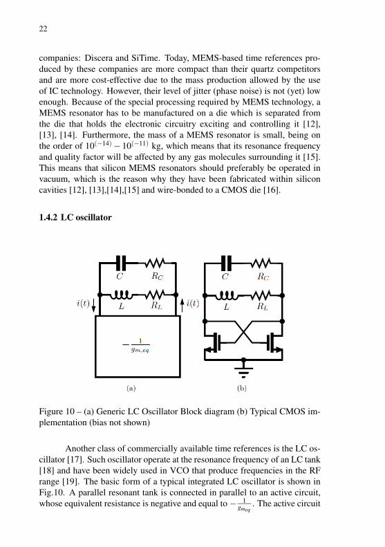
Figure 10 – (a) Generic LC Oscillator Block diagram (b) Typical CMOS im-plementation (bias not shown)
Another class of commercially available time references is the LC os-cillator [17]. Such oscillator operate at the resonance frequency of an LC tank[18] and have been widely used in VCO that produce frequencies in the RFrange [19]. The basic form of a typical integrated LC oscillator is shown inFig.10. A parallel resonant tank is connected in parallel to an active circuit,whose equivalent resistance is negative and equal to− 1
gmeq. The active circuit

23
compensates for the losses of the tank and sustains the oscillation. In the tank,both the coil of inductance L and the capacitor of capacitance C exhibit finitelosses, modeled respectively by series resistances RL and RC. The frequencyof oscillation is given by equation.(1.2),
f = f0.
√√√√√1− C.R2L
L
1− C.R2C
L
= f0
√1− 1
Q2L√
1− 1Q2
C
(1.2)
where QL = 2.π. f .LRL
and QC = 12.π.L.RC
are the inductor and the capacitor qual-ity factor, respectively. f0 is the tank natural resonant frequency given byequation.(1.3):
f0 =1
2.π.√
LC(1.3)
The LC oscillator is usually used as a time reference. In this case,special attention needs to be paid to the stability of the output frequency as afunction of process, temperature and voltage variations. As shown in Fig10,an LC oscillator is based on passive elements such as inductors and capacitorsas well as active elements, i.e. transistors. Therefore, such an oscillator can bemade in a standard CMOS process. The first steps towards commercializingself-referenced LC oscillators were taken at Mobius Microsystems, a fablesscompany founded in 2004 with the aim of developing all-silicon frequencysources that replace quartz crystal oscillators. The goal of Mobius Microsys-tems was to produce a monolithic free-running RF LC oscillator that did notrequire the frequency synthesizers used in MEMS time references. This wasto avoid the effect of multiplication on the output frequency jitter. These ef-forts resulted in oscillators with output frequency ranges from 12 to 25 MHzand with initial target applications such as wire-line data communication, e.g.,USB. An LC oscillator based on the resonant tank shown in Fig.10 not onlysuffers from frequency deviation due to the losses, but also due to variationsin the absolute values of the passive elements due to process and temperature.
1.4.3 Relaxation oscillator with positive feedback
Oscillators with positive feedback as the one shown in Fig.11, have tosatisfy the Barkhausen criteria which can be stated as follows:
If A is the gain of the amplifying element and β ( jw) is the transferfunction of the feedback path, the circuit will sustain steady oscillations onlyat frequencies for which:

24
Figure 11 – Amplifier in close loop
• The loop gain is equal to unity in absolute magnitude, that is, |A.β |= 1
• The phase shift around the loop is zero or an integer multiple of 2π .
Barkhausen’s criteria is a necessary condition for oscillation but not asufficient condition: some circuits satisfy the criteria but do not oscillate.
Figure 12 – Current-starved ring oscillator
In the case of the ring oscillator such as the one in Fig.12, the oscil-lation frequency depends on the delay τd in each stage and on the number ofstages m in the ring oscillator, according to
fd =1
2.m.τd(1.4)
In order to use a ring oscillator as time reference, some form of com-pensation of supply voltage variations must be employed locally. The use ofa low drop-out (LDO) regulator which provides a stable local output voltageis one of the options [20].
In Fig.13 we have one example of ring oscillator with a specific circuitto generate a stable local supply voltage.

25
Figure 13 – RC + Ring Oscillator [20]
The period of oscillation is given by,
T0 = RC.ln((1+KSW )(2−KSW )
KSW (1−KSW )) (1.5)
where KSW =VSW/Vdd . VSW is the switching point of the inverter one (INV1).In [20] the implemented RC oscillator consists of an RC network, and aninverting gain element from a resistor terminal to a capacitor terminal andanother inverting gain element from the common resistor/capacitor terminalback to the resistor terminal. For high gain, the two inverting elements consistof three and five inverters, respectively. A simple regulator, consisting of anNMOS voltage follower and a replica inverter that is flipped and biased bya reference current, produces a local regulated supply for the inverters. Theflipped replica of inverter is formed by a PMOS in diode configuration and aNMOS in saturation. Then the voltage at the drain of the NMOS in the flippedinverter is equal to, VD f lipped ≈
IPTATVE .L
, where VE is the early voltage which islinear function of the temperature. Then to make the voltage at the drain ofthe NMOS in the flipped inverter independent with temperature variation, theauthor polarized the flipped inverter with a PTAT current. Consequently thevoltage at the drain of the NMOS in the flipped inverter is a voltage referenceindependent with temperature and using a NMOS voltage follower allows tobias the oscillator with local supply voltage. This local supply is well belowthe standard core voltage for the technology 65 nm, used in this relaxationoscillator. It is designed an RC circuit together with a Ring oscillator, wherethe oscillation period is defined by the period of the ring oscillator plus theperiod of the RC oscillator. But this topology is designed for the period of
26
the RC oscillator greater than the period of the ring oscillator. The thresholdvoltage VSW is used as switch point of the charge and discharge of the capac-itor. One disadvantage of this topology is that the switch point of the inverterdepends strongly on process, supply voltage and temperature variations.
1.4.4 Relaxation oscillator using comparators
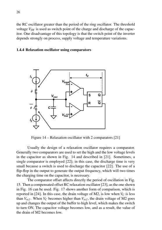
Figure 14 – Relaxation oscillator with 2 comparators [21]
Usually the design of a relaxation oscillator requires a comparator.Generally two comparators are used to set the high and the low voltage levelsin the capacitor as shown in Fig. 14 and described in [21]. Sometimes, asingle comparator is employed [22]; in this case, the discharge time is verysmall because a switch is used to discharge the capacitor [22]. The use of aflip-flop in the output to generate the output frequency, which will two timesthe charging time on the capacitor, is necessary.
The comparator offset affects directly the period of oscillation in Fig.15. Then a compensated offset RC relaxation oscillator [23], as the one shownin Fig. 16 can be used. Fig. 17 shows another form of comparison, which isreported in [24]. In this case, the drain voltage of M2, is low when VC is lessthan Vre f . When VC becomes higher than Vre f , the drain voltage of M2 goesup and changes the output of the buffer to high level, which makes the switchto turn ON. The capacitor voltage becomes low, and as a result, the value ofthe drain of M2 becomes low.

27
Figure 15 – Relaxation Oscillator using one comparator only [22]
Figure 16 – Relaxation oscillator with one comparator and compensated Off-set [23]
1.4.5 Mobility-based relaxation oscillator
Some authors have designed the period of oscillation directly propor-tional to the mobility. In [25], a class of low-power time references based onthe mobility of MOS transistors has been introduced (Fig.18). Such referencedissipates micro watts of power and achieve inaccuracies of the order of a fewpercent.
The implementation described in [25] is targeted to wireless sensornetworks. It has an output frequency of 150 kHz, dissipates 42.6 µW from
28
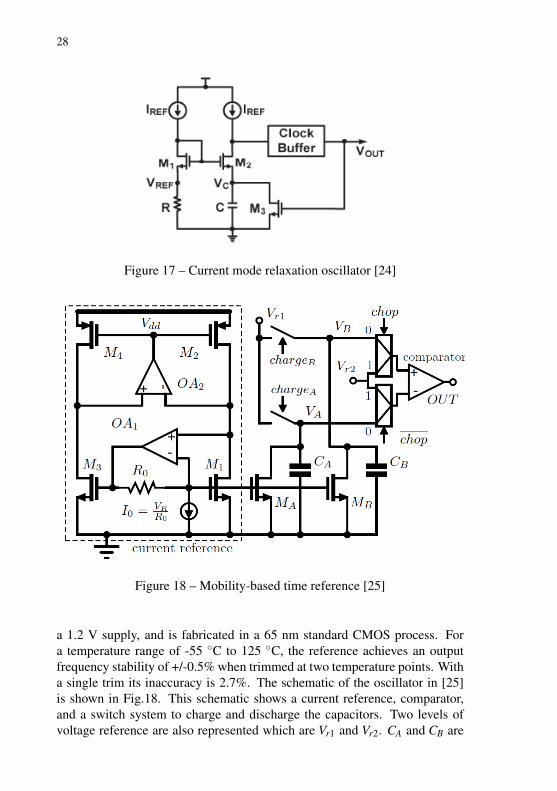
Figure 17 – Current mode relaxation oscillator [24]
Figure 18 – Mobility-based time reference [25]
a 1.2 V supply, and is fabricated in a 65 nm standard CMOS process. Fora temperature range of -55 ◦C to 125 ◦C, the reference achieves an outputfrequency stability of +/-0.5% when trimmed at two temperature points. Witha single trim its inaccuracy is 2.7%. The schematic of the oscillator in [25]is shown in Fig.18. This schematic shows a current reference, comparator,and a switch system to charge and discharge the capacitors. Two levels ofvoltage reference are also represented which are Vr1 and Vr2. CA and CB are

29
Figure 19 – Waveform of the mobility-based time reference [25]
alternatively pre-charged to Vr1 and then linearly discharged by MA and MB.When the voltage on the discharging capacitor drops below Vr2, the output ofthe comparator switches and the linear discharge of the other capacitor startsimmediately Fig.19. The author of this relaxation oscillator considers that themobility is less sensitive with temperature variation at high doping level.
Another mobility-based oscillator [22] has been implemented in a 0.35µm CMOS, and this oscillator has an output frequency of 3.3 kHz, and con-sumes 11 nW from 1 V supply voltage and a accuracy greater than 1% withtemperature variation (-20 ◦C to 80 ◦C). In [22] the author considers that themobility is inversely proportional to temperature variation, which could becompensated by the thermal voltage. But how does the mobility varies interm of the temperature in MOSFET devices ?
In the next section we present some theory about mobility dependenceon temperature and, finally, we show the simulated behavior of the mobilitywith respect to temperature in the IBM 180 nm technology.
1.5 MOBILITY IN MOSFETS
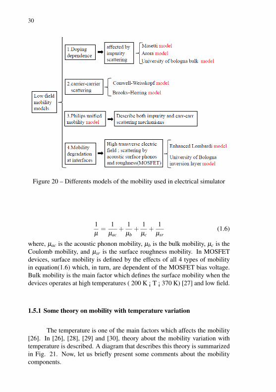
Mobility was one of the most studied MOSFET parameters in the early1980s. Fig.20 shows a summary of different models commonly used in elec-trical simulators for mobility in silicon.
The mobility can be written [26] as :
30
Figure 20 – Differents models of the mobility used in electrical simulator
1µ
=1
µac+
1µb
+1µc
+1
µsr(1.6)
where, µac is the acoustic phonon mobility, µb is the bulk mobility, µc is theCoulomb mobility, and µsr is the surface roughness mobility. In MOSFETdevices, surface mobility is defined by the effects of all 4 types of mobilityin equation(1.6) which, in turn, are dependent of the MOSFET bias voltage.Bulk mobility is the main factor which defines the surface mobility when thedevices operates at high temperatures ( 200 K ¡ T ¡ 370 K) [27] and low field.
1.5.1 Some theory on mobility with temperature variation
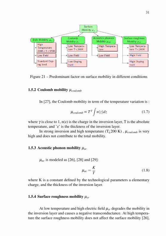
The temperature is one of the main factors which affects the mobility[26]. In [26], [28], [29] and [30], theory about the mobility variation withtemperature is described. A diagram that describes this theory is summarizedin Fig. 21. Now, let us briefly present some comments about the mobilitycomponents.
31
Figure 21 – Predominant factor on surface mobility in different conditions
1.5.2 Coulomb mobility µcoulomb
In [27], the Coulomb mobility in term of the temperature variation is :
µcoulomb ∝ T γ
∫n(z)dz (1.7)
where γ is close to 1, n(z) is the charge in the inversion layer, T is the absolutetemperature, and ’z’ is the thickness of the inversion layer.
In strong inversion and high temperature (T¿200 K) , µcoulomb is veryhigh and does not contribute to the total mobility.
1.5.3 Acoustic phonon mobility µac
µac is modeled as [26], [28] and [29]:
µac =KT
(1.8)
where K is a constant defined by the technological parameters a elementarycharge, and the thickness of the inversion layer.
1.5.4 Surface roughness mobility µsr
At low temperature and high electric field µsr degrades the mobility inthe inversion layer and causes a negative transconductance. At high tempera-ture the surface roughness mobility does not affect the surface mobility [26],

32
[28], [29], [30].
1.5.5 Bulk mobility µb
Fig. 21 summarizes the dominant effect in terms of the temperatureand the doping level. In [30] the bulk mobility is modeled in function of thedoping level and the temperature as,
µb(NA,T )≈ µ0 +µmax−µ0
1+(NACr)α
(1.9)
andµmax = µ0(
TT0
)−γ (1.10)
Cr and Cl are constants NA is the doping level of the bulk, µ0 is the mobility atT0, γ is a coefficient dependent of the doping level. Some authors [30] reportthat 1.5 < γ < 2.3.
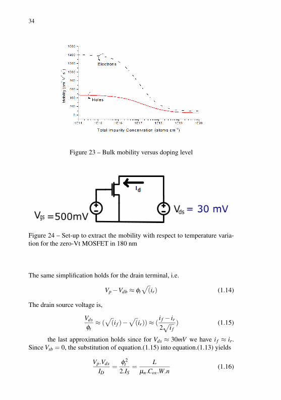
From equation.1.9, we can see that, at high doping level, the bulk mo-bility will be less sensitive to temperature variation. At low doping level thebulk mobility is more or less CTAT i.e., complementary to absolute temper-ature. In Fig.22 and Fig.23, we can see that at low doping level the mobilitydecreases linearly when the temperature increases, and is less dependent withprocess variation. At high doping level the mobility is more or less constantwith respect to temperature variation but depends heavily on doping .
1.5.6 Simulation of mobility with respect to temperature variation
To measure carrier mobility in the inversion layer of the MOSFETs,large devices are commonly chosen to avoid short-channel and narrow-widtheffects. In this work we have used W = 3µm, L = 20X3µm device to extractthe mobility from simulation in 180 nm, which corresponds to the dimensionsof the MOSFET used as a resistor in the voltage-controlled current source ofthe time reference. Generally two methods could be used to extract the mo-bility in MOSFET namely the DC current method and the split CV methods.The split CV method can overestimate the mobility due to parasite capac-itances in MOSFET. We have used the drain current method to extract themobility.
The DC current method allows the extraction of the mobility in strong

33
Figure 22 – : Bulk mobility variation with temperature at different dopinglevels
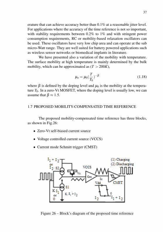
inversion. This mobility is called a conductivity mobility and is related to thechannel conductance. The circuit for measuring the channel conductance isshown in Fig.24.
gds =∆Id
∆Vds(1.11)
Using the UCCM from ACM [31] (Advanced Compact Model, see appendixfor details) of MOSFET: yields:
Vp−Vsb = φt(√
1+ i f −2+ ln(√
1+ i f −1)) (1.12)
In strong inversion the logarithm term can be neglected; thus, equation(1.12)can be written as
Vp−Vsb ≈ φt√(i f ). (1.13)
34
Figure 23 – Bulk mobility versus doping level
Figure 24 – Set-up to extract the mobility with respect to temperature varia-tion for the zero-Vt MOSFET in 180 nm
The same simplification holds for the drain terminal, i.e.
Vp−Vdb ≈ φt√(ir) (1.14)
The drain source voltage is,
Vds
φt≈ (
√(i f )−
√(ir))≈ (
i f − ir2.√
i f) (1.15)
the last approximation holds since for Vds ≈ 30mV we have i f ≈ ir.Since Vsb = 0, the substitution of equation.(1.15) into equation.(1.13) yields
Vp.Vds
ID=
φ 2t
2.IS=
Lµn.Cox.W.n
(1.16)

35
Which can be writen as,
µn =L.ID
Cox.W.Vp.Vds.n. (1.17)
where Vp =Vgs−Vth
n is called the pinch-off voltage. Vth is the threshold voltageas defined in appendix A. To extract the mobility and the threshold voltagewe have fixed the value of Vds = 30mV , we have plotted Id vs Vgs for differenttemperature. For Vgs = 500mV , we have extrapolated a line for this point andtangent to Id vs Vgs with a specific temperature. The point of intersection ofthis line and x-axis determine the threshold voltage at the specific tempera-ture. From the curve Id vs Vgs one can get the value of Id which correspondsto Vgs = 500mV . After getting this threshold voltage and the value of thecurrent using equation.(1.17), one can determine the mobility. In zero-Vt de-vices the threshold voltage is near zero but it will vary with the temperature.Fig.25 shows the simulated normalized mobility variation and the thresholdvoltage variation with respect to temperature variation. The normalized mo-bility variation is defined for the value of the mobility at temperature T0 = 27◦C as reference.
Figure 25 – Simulation result of the mobility with temperature in zero-VtMOSFET device
1.6 COMPARISON BETWEEN TECHNIQUES AVAILABLE TO GENER-ATE TIME REFERENCES
This chapter provided an overview of various types of silicon-basedtime references and some theory about mobility variation with respect to tem-perature variation.

36
Table 1 – Comparison between techniques to generate time referencesOscillator MEMS Oscillator [12] LC Oscillator [32] Crystal oscillator [33] Relax oscillator [25]Location In-package On-chip On-Board On-chipF-Variation +/−10ppm +/−100ppm +/−1ppm/200ppm +/−10000ppmFrequency-F 200KHz-200 MHz GHz 1 KHz- 100 MHz 1KHz-10MHzCURRENT(IQ) 5mA - 50 mA 10 mA 100 nA - 50 mA 10 nA - 100 µAIQ/F High @ KHz Medium @ MHz Low Medium @KHz High @ MHz LowCOST HIGH Low Medium LowTemp -40◦C to 85 ◦C -40◦C to 125◦C -20◦C to 60 ◦C -40◦C to 100 ◦C
In the first part we presented the state-of-the-art of techniques avail-able to generate time reference. These included crystal oscillator, MEMS-resonator-based oscillators, LC oscillators, RC harmonic oscillators, RC re-laxation oscillators, ring oscillators and finally electron-mobility-based oscil-lators. Each approach has its own specific advantages and disadvantages. Tomake a comparison, it is helpful to summarize the performance characteris-tics for each type of time reference. One of the difficulties in providing acomplete and fair comparison between published time references is that of-ten insufficient data on their performance over process and temperature hasbeen provided. There are references in which the performance of a singledevice has been reported as a measure of stability, which does not allow afair comparison with references for which more samples have been charac-terized. From the previously described types of silicon-based time references,a performance summary of those with the most complete results is presentedin Table 1. MEMS-resonator-based oscillators and LC oscillators have beencommercialized, and thus their reported performance characteristics are atproduction level. The characteristics of other topologies are obtained mainlyfrom publications. It can be seen that MEMS-based oscillators achieve thebest accuracy over the widest temperature range. Their form factor has alsobeen shrunk and they are physically smaller than crystal oscillators. How-ever, their major disadvantage is the need for special MEMS processing. Thisrequires a two-die solution, in which the MEMS resonator is wire bonded toanother CMOS chip. The power consumption of MEMS oscillators is compa-rable to that of LC oscillators and is larger than the other types. Apart from theMEMS-based oscillators and crystal oscillator, all the other time referencesin Table. 1 are standard CMOS compatible, which is a great advantage as faras manufacturing, packaging costs and complexity are considered. Amongthese, LC oscillators achieve the best accuracy over process and temperature,as well as the best jitter performance. However, their power consumption ishigher than that of the other oscillators and their temperature range is the nar-rowest. MEMS-based and LC-based oscillators are the only solutions in lit-
37
erature that can achieve accuracy better than 0.1% at a reasonable jitter level.For applications where the accuracy of the time reference is not so important,with stability requirements between 0.2% to 1% and with stringent powerconsumption requirements, RC or mobility-based relaxation oscillators canbe used. These oscillators have very low chip area and can operate at the submicro-Watt range. They are well suited for battery powered applications suchas wireless sensor networks or biomedical implants in literature.
We have presented also a variation of the mobility with temperature.The surface mobility at high temperature is mainly determined by the bulkmobility, which can be approximated as (T > 200K),
µn = µ0(TT0
)−β (1.18)
where β is defined by the doping level and µ0 is the mobility at the tempera-ture T0. In a zero-Vt MOSFET, where the doping level is usually low, we canassume that β ≈ 1.5.
1.7 PROPOSED MOBILITY-COMPENSATED TIME REFERENCE
The proposed mobility-compensated time reference has three blocks,as shown in Fig.26:
• Zero-Vt self-biased current source
• Voltage controlled current source (VCCS)
• Current mode Schmitt trigger (CMST)
Figure 26 – Block’s diagram of the proposed time reference

38
In chapter 2 to 4 we describe the main sub-circuits that are used inthe proposed time reference which is presented in chapter 5. A self-biasedcurrent source with zero-Vt is presented in chapter 2. The subject of chapter3 is a voltage-controlled current source, while a current mode Schmitt-triggeris the subject of the chapter 4. The time reference which makes use of thesub-circuits in chapter 2-4 is described in chapter 5.

39
2 ZERO-VT SELF-BIASED CURRENT SOURCE (SBCS)
A Self-biased current source can be implemented as an extractor cir-cuit of the specific current of a MOSFET. The specific current generator wasproposed in [34], as an alternative to have a stand-alone reference ultra-lowpower consumption. A design methodology using a transistor model of theMOSFET valid in all operating regions was also introduced in the paper.
This chapter is divided in three sections. In the first section we givesome information about the design of the self-biased current source; in thesecond section we design a zero-Vt self-biased current source and, finally, wehave the simulated results of the zero-Vt SBCS.
2.1 SELF-BIASED CURRENT SOURCE (SBCS) DESIGN
Figure 27 – Full schematic of the self-biased current source
In Fig.27 we show the schematic of the self-biased current source [31],which can be divided in two parts. One of them is the voltage-followingcurrent mirror M4, M5, M7 and M8, while the self-cascode MOSFET (SCM)composed by M1 and M2. The Advanced Compact Model (ACM) describedin appendix A has been used to design the SBCS [34], [31].
40
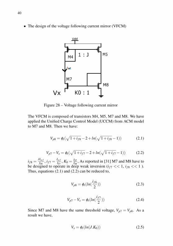
• The design of the voltage following current mirror (VFCM)
Figure 28 – Voltage following current mirror
The VFCM is composed of transistors M4, M5, M7 and M8. We haveapplied the Unified Charge Control Model (UCCM) from ACM modelto M7 and M8. Then we have:
Vp8 = φt(√
1+ i f 8−2+ ln(√
1+ i f 8−1)) (2.1)
Vp7−Vx = φt(√
1+ i f 7−2+ ln(√
1+ i f 7−1)) (2.2)
i f 8 =JIre fIS8
, i f 7 =Ire fIS7
, K0 =IS7IS8
, As reported in [31] M7 and M8 have tobe designed to operate in deep weak inversion (i f 7 << 1, i f 8 << 1 ).Thus, equations (2.1) and (2.2) can be reduced to,
Vp8 = φt(ln(i f 8
2)) (2.3)
Vp7−Vx = φt(ln(i f 7
2)) (2.4)
Since M7 and M8 have the same threshold voltage, Vp7 = Vp8. As aresult we have,
Vx = φt(ln(J.K0)) (2.5)
41
The PMOS transistors were designed to operate in weak inversion toallow low voltage application.
• Design of the SCM composed of M1 and M2
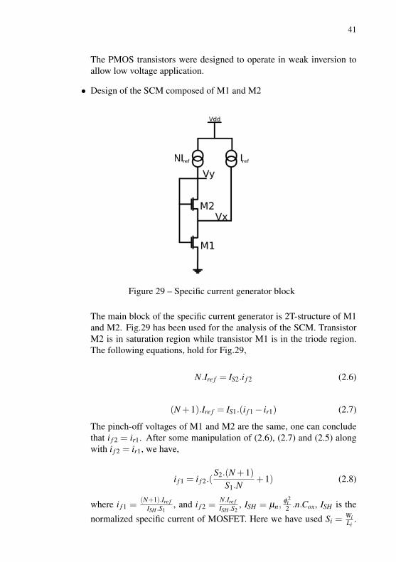
Figure 29 – Specific current generator block
The main block of the specific current generator is 2T-structure of M1and M2. Fig.29 has been used for the analysis of the SCM. TransistorM2 is in saturation region while transistor M1 is in the triode region.The following equations, hold for Fig.29,
N.Ire f = IS2.i f 2 (2.6)
(N +1).Ire f = IS1.(i f 1− ir1) (2.7)
The pinch-off voltages of M1 and M2 are the same, one can concludethat i f 2 = ir1. After some manipulation of (2.6), (2.7) and (2.5) alongwith i f 2 = ir1, we have,
i f 1 = i f 2.(S2.(N +1)
S1.N+1) (2.8)
where i f 1 =(N+1).Ire f
ISH .S1, and i f 2 =
N.Ire fISH .S2
, ISH = µn,φ2
t2 .n.Cox, ISH is the
normalized specific current of MOSFET. Here we have used Si =WiLi
.
42
From equation. (2.8), one can conclude that if Vx is PTAT, then Ire f is acopy of the specific current. Conversely, if Ire f is a copy of the specificcurrent then Vx is PTAT.
2.2 ZERO-VT SELF-BIASED CURRENT SOURCE
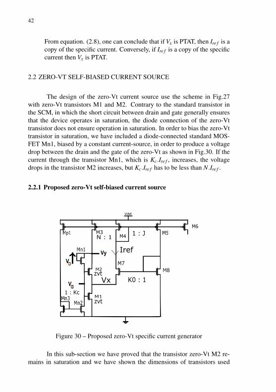
The design of the zero-Vt current source use the scheme in Fig.27with zero-Vt transistors M1 and M2. Contrary to the standard transistor inthe SCM, in which the short circuit between drain and gate generally ensuresthat the device operates in saturation, the diode connection of the zero-Vttransistor does not ensure operation in saturation. In order to bias the zero-Vttransistor in saturation, we have included a diode-connected standard MOS-FET Mn1, biased by a constant current-source, in order to produce a voltagedrop between the drain and the gate of the zero-Vt as shown in Fig.30. If thecurrent through the transistor Mn1, which is Kc.Ire f , increases, the voltagedrops in the transistor M2 increases, but Kc.Ire f has to be less than N.Ire f .
2.2.1 Proposed zero-Vt self-biased current source
Figure 30 – Proposed zero-Vt specific current generator
In this sub-section we have proved that the transistor zero-Vt M2 re-mains in saturation and we have shown the dimensions of transistors used
43
in the zero-Vt self-biased current source. To prove that M2 will remain insaturation, we have applied UCCM to M2, in the source we have:
Vp2−Vx = φt(√
1+ i f 2−2+ ln(√
(1+ i f 2)−1)) (2.9)
In the drain of M2 we have:
Vp2−Vy = φt(√
1+ ir2−2+ ln(√(1+ ir2)−1)) (2.10)
To keep the transistor M2 in saturation we have to design Vy and Vx to satisfythe condition Vy−Vx > VdsatM2 and Vy = VD +VG. Then VD and VG are de-signed such away to allow that VD +VG−Vx > VdsatM2 , With VD ≈ 200mV ,VG ≈ 200mV and Vx ≈ 60mV . We have considered that M2 is in satura-tion when the drain-source voltage of M2 is greater than VdsatM2 = 200mV ,consequently one can consider that the transistor M2 is in saturation sinceVdsatM2 < (VD +VG −Vx = 340mV ). Using the same logic in section.2.1equation.(2.8) but considering that the current through the transistor M2 is(N−Kc).Ire f , one can deduce that,
i f2 [(N−Kc +1
N−Kc).
S2
S1+1] = i f1 . (2.11)
From equation.(2.5) Vx = φt ln(J.K0), then we can apply UCCM to M1and M2,
φt .F(i f1)−φt .F(i f2) =Vx. (2.12)
where F(i f i) = φt(√
1+ i f i−2+ ln(√
1+ i f i−1))Combining equations.(2.11) and (2.12) we got,
φt .F(i f 2[(N−Kc +1
N−Kc).
S2
S1+1])−φt .F(i f 2) =Vx (2.13)
We have fixed the parameters N = 2 , Kc = 1, J = 0.5, K0 = 8 and S2S1
= 2.5.As we have fixed J = 0.5 and K0 = 8 then Vx = φt .ln(J.K0) = 1.38.φt .
From equation.(2.13) we can determine the value of i f 2 = 26. From equa-tion.(2.11) we can determine the inversion level of i f 1 = 40. Table 2 resumethe width and the length of the zero-Vt self-biased current source. M7 andM8 are designed in deep weak inversion then i have used a wide width, andM3, M4, M5, are designed in deep weak inversion.
44
Table 2 – Width and length of the zero-Vt Self-Biased current sourceWidth Length
M1 3 µm 3 µm x 5M2 3 µm 3 µm x 5M3 5 µm x 2 3 µmM4 5 µm 3 µmM5 5 µm 3 µm x 2M7 13 µm x 8 3 µmM8 13 µm 3 µmMn1 10 µm 3 µmMn2 10 µm 3 µmMn3 10 µm 3 µmMp1 5 µm 3 µm
2.2.2 Simulation result of the zero-Vt Self-Biased current source
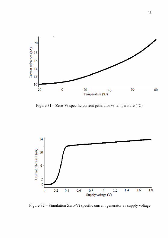
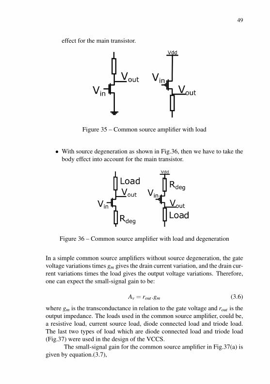
The simulation result of the self-biased current source using analog en-vironment 180 nm CMOS technology is shown in Fig.31 and Fig.32. Fig.31shows the simulation result of the current reference with respect to temper-ature variation. We can see that at -20◦ C the current reference is around10 nA and at 80 ◦ C the current reaches almost linearly the value of 20 nA.This current reference is the specific current of the zero-Vt. The variationof the specific current with respect to the temperature variation is defined bythe term µn.φ
2t , where µn = µ0(
TT0)−β , one can conclude that the value of β
should be less than 1 and greater than 0.6 to obtain the variation with respectto temperature as shown in Fig.31 (we have considered that the slope factorand the oxide capacitance are temperature independent). Fig.32 shows thecurrent reference with respect to supply voltage variation. the minimum sup-ply voltage is around 0.4 V and the maximum is 1.8 V. A global variation of1 nA can be observed in Fig.32.
45
Figure 31 – Zero-Vt specific current generator vs temperature (◦C)
Figure 32 – Simulation Zero-Vt specific current generator vs supply voltage

46

47
3 VOLTAGE-CONTROLLED CURRENT SOURCE
A voltage-controlled current source is an electronic component whichconverts linearly a voltage to a current. The voltage controlled current sourcethat we have used, can be divided in 2 basic building blocks, an operationaltransconductance amplifier (OTA) and a common source amplifier with diodeconnected load. This chapter is divided in three sections, in the first sectionwe present the OTA design, in the second section the common source ampli-fier and, finally, the voltage controlled current source.
3.1 OPERATIONAL TRANSCONDUCTANCE AMPLIFIER DESIGN
Figure 33 – Operational transconductance amplifier
The operational transconductance amplifier, shown in Fig.33, is a de-vice that generates at its output a current that is a linear function of the differ-ential input voltage.
Ideally, the output current is given by
Iout =Vdi f f .Gm (3.1)
Gm is the equivalent transconductance of the OTA.When the load of the OTA is a capacitance we have in this case, the

48
output impedance is given by,
1rout
= gmd11 +gmd14 (3.2)
and the band-width of the OTA is,
BW =1
2.π.rout .Cload(3.3)
the gain A1 of the OTA is ,
A1 =gm14
gmd14 +gmd11(3.4)
and the gain band-width is,
GBW =gm13
2.π.Cload(3.5)
The OTA has to be high gain, then we have designed the transistors M13 andM14 in weak inversion, in this case gm14 ≈
Ipφt
, and we have used long length
in the transistors M11 and M12 then the output resistance 1rout
=Ip
VE .L, where
the VE is the early voltage and L = 3µm is the length of the transistor andIp = 20nA is the polarization current of the OTA.
3.2 COMMON SOURCE AMPLIFIER WITH ACTIVE LOAD
In common source amplifier, the input is connected to the gate and theoutput taken from the drain
Figure 34 – Common source amplifier
In Fig.34, we have the simple topology of the common source ampli-fier. We can divide a common source amplifier into two groups:
• Without source degeneration as shown in Fig.35, then we have no body
49
effect for the main transistor.
Figure 35 – Common source amplifier with load
• With source degeneration as shown in Fig.36, then we have to take thebody effect into account for the main transistor.
Figure 36 – Common source amplifier with load and degeneration
In a simple common source amplifiers without source degeneration, the gatevoltage variations times gm gives the drain current variation, and the drain cur-rent variations times the load gives the output voltage variations. Therefore,one can expect the small-signal gain to be:
Av = rout .gm (3.6)
where gm is the transconductance in relation to the gate voltage and rout is theoutput impedance. The loads used in the common source amplifier, could be,a resistive load, current source load, diode connected load and triode load.The last two types of load which are diode connected load and triode load(Fig.37) were used in the design of the VCCS.
The small-signal gain for the common source amplifier in Fig.37(a) isgiven by equation.(3.7),

50
Figure 37 – (a)NMOS common source amplifier with diode connected load(b) PMOS common source amplifier with NMOS load in triode
A2 =gm10
gm15 +gmd15 +gmd10(3.7)
and the small signal for the common source amplifier in Fig.37(b) is given byequation.(3.8)
A3 =gm16
gmd16 +gmd9(3.8)
3.3 VOLTAGE CONTROLLED CURRENT SOURCE
The simple voltage controlled current source (VCCS), formed by theOTA , and the common source amplifier is shown in Fig.38.
Figure 38 – Schematic of the voltage controlled current source block
But this topology has the body effect on the main transistor of thecommon source amplifier which is represented by M10. This body effectreduces the small-signal gain of the transistor M10. To avoid this fact, wehave done some modifications on the topology in Fig.38 as shown in Fig.39.

51
We have transformed the transistor M10 in common source amplifier withoutbody effect. Then we can emulate high value of resistor in M9 increasing thevalue of Kr.
Figure 39 – Schematic of the voltage controlled current source block
Fig.40 shows the full schematic of the voltage controlled current source.The capacitor C is used for overall stability and its value is 500 fF. A1 is theOTA gain, A2 is the gain of the common source amplifier with diode con-nected load and, A3 is the gain of the common source amplifier with load intriode.
Figure 40 – Voltage controlled current source (the capacitor C is for overallstability)

52
One can express the open loop gain as follow,
V1 = A1(Vc−V3) (3.9)V2 = A2.V1 (3.10)V3 = A3.V2 (3.11)
From equations (3.9), (3.10) and (3.11), we have:
V3.(1+A3.A2.A1) = A3.A2.A1.Vc (3.12)
V3(1
A3.A2.A1+1) =Vc (3.13)
From equation.(3.13) we can say that, if the open loop gain defined as A1.A2.A3 >>1 then,
Vc ≈V3. (3.14)
Where A1, A2 and A3 are defined previously.We have used zero-Vt MOSFET as resistor then the current in this
resistor will be defined by Vc as, Ic =Vc.gmd9.
3.3.0.1 Comments on the nonlinear characteristic of the MOSFET
The output characteristic I-VDS of the MOSFET shows two regions[31]. The MOSFET operates as current source in saturation and as a resistorin the triode region. When a MOSFET is used as a resistor we have a non-linear behavior at some drain-source voltage of the resistor. This limits therange of Vc that we can operate the MOSFET as resistor. The MOSFET asresistor is modeled and reported in [31],
gmd9 =2.IS
φt.(√
1+ ir9−1) (3.15)
In Fig.40, the transistor M9 is biased by a gate voltage VG as definedin Fig.30. In the chapter.5 we have explained the reason of the use of thisVG. From equation.(3.15), the stability of the MOSFET as resistor gmd9, de-pends strongly with the variation of the specific current of the MOSFET. Inchapter 1, we have discussed about mobility variation with temperature andprocess variations due to the fact that the specific current depends stronglywith the mobility variation. Fig.23 and Fig.22 show the mobility variationwith process and temperature variations. And one can interpret that at lowdoping level the bulk mobility is independent with process variation and itsvalue decreases linearly when the temperature increases. To verify this in-
53
terpretation we have plotted the output I-V characteristic of the MOSFET atdifferent temperature for the native (zero-Vt) MOSFET, for the case whereVGB =Vth Fig.41 shows the set up,
Figure 41 – Setup to plot the output characteristic of the zero-Vt (IdvsVds)
Vth is the threshold voltage of the zero-Vt MOSFET. We have extractedthe threshold voltage using gm
Idmethod at different temperatures as shown in
Fig.25. When VGB =Vth, the equivalent inversion level is ir = 3, then we can
write that [31], gmd = 2.ISφt
= µn.φt .C′ox.n.W
L . Table.3 summarize the length andwidth used in this voltage controlled current source.
Table 3 – Width and length of the voltage controlled current sourceWidth (µm ) Length(µm )
M9 3 20x3M10 3 3M11 3 3M12 3 3M13 10 3M14 10 3M15 3 3M16 3 3

54

55
4 CURRENT MODE SCHMITT TRIGGER (CMST)
The current-mode Schmitt trigger is composed of switches and a cur-rent comparator. In this chapter we present some state-of-the-art of currentcomparators and the proposed current-mode Schmitt trigger.
4.1 STATE-OF-THE-ART OF CURRENT COMPARATORS
Figure 42 – Freita’s comparator [35]
Figure 43 – Traff’s comparator [36]
In many cases, the signals from sensors are currents [37], [38], [39].Also, the output signal from a transistor is a current. Thus a current com-parator is often required to process directly the signal from sensors or fromtransistors. As in any decision circuitry, accuracy, power, and high speed

56
are important parameters of comparators. Additionally, current comparatorsmust work over a wide range of supply voltages, wide range of temperatures,and not be sensitive to process variation. Also it should not have a dead zonein the transfer characteristic. A very simple current comparator is shown inFig.42 [35], but this current comparator has long delay when operated at lowcurrents.
Reference [36] presents the most referenced current comparator, knownas Traff’s comparator and shown in Fig. 43. This current comparator is highspeed and has low input impedance. The feedback operation of this circuitdoes not allow the input node to rise from rail to rail, and this increases thespeed of the comparator. But Traff’s comparator has a dead zone. Since thepublication of the Traff’s comparator a number of designs [40], [41], [42] hasbeen tried to achieve the high speed, low power and no dead zone. In [43],[44], two different classes of AB current comparator, free of dead zone, werepublished. But the minimum supply voltage has to be one threshold voltageof NMOS plus two saturation levels, which is not suitable for low voltageapplication. Also these current comparators, shown in Fig.44, Fig.45, need aclock to operate .
Figure 44 – Class AB current comparator with switch [43]
The comparator in Fig.44 [43], has two inputs; I1, and I2. When theclock signal φ is high, the circuit works as a current conveyor which is acombination of voltage and current follower. Transistors from M1 to M6form a translinear loop, which fixes the quiescent current of the branches andthe input node voltage at the ground potential. Transistors M7, M8, M10 and
57
Figure 45 – Class AB current comparator with compensation circuit [44]
M11 constitute two latches and they have a regenerative operation when φ
goes down. Transistors M7, M9 and M10, M12 operate as current mirror.To explain how the topology in Fig.44 works, we have considered followingcases with Vdd =−Vss,
• φ = 0, then switches S1 and S2 are opened and S3 is closed.
– I1 = 0 and I2 = 0, The current through the transistors M2, M4,M5 and M6 is I0. The diodes D1 and D2 limit the voltage in thedrain-source of the transistor M2, M4 and M5, M6 respectively.This allows that the increase of the current I1(I2) does not increaseso much the drain-source of M4 and M2(M5 and M6).
– I1 > I2, the drain-source voltage of the transistor M7 increasesand the drain-source voltage of the transistor M8 decreases. Thesource-drain voltage of M10 increases and the source-drain volt-age of M11 decreases. This results in the fact that the transistorM9 is ON and the transistor M12 is OFF. Consequently the outputgoes to Vss.
– I1 < I2, the drain-source voltage of M8 increases and the drain-source voltage of M7 decreases and the source-drain voltage of
58
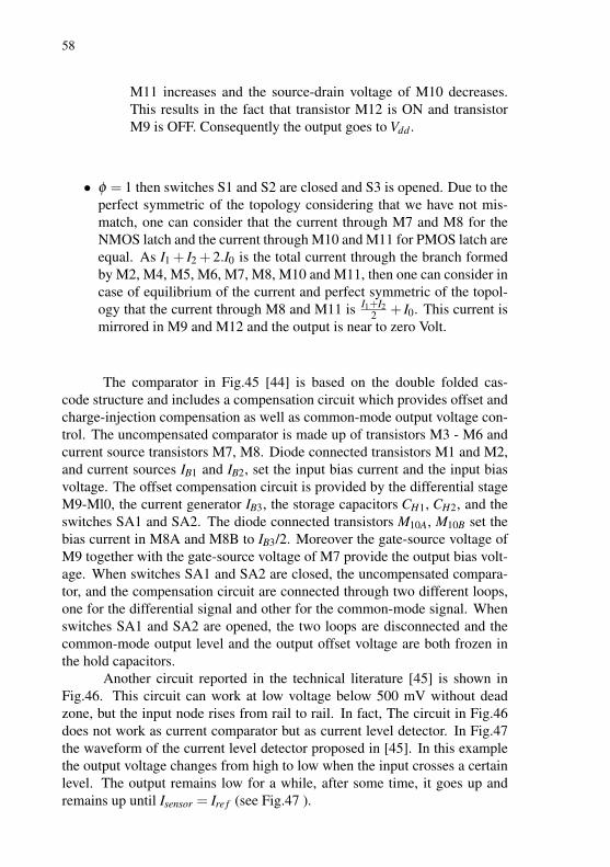
M11 increases and the source-drain voltage of M10 decreases.This results in the fact that transistor M12 is ON and transistorM9 is OFF. Consequently the output goes to Vdd .
• φ = 1 then switches S1 and S2 are closed and S3 is opened. Due to theperfect symmetric of the topology considering that we have not mis-match, one can consider that the current through M7 and M8 for theNMOS latch and the current through M10 and M11 for PMOS latch areequal. As I1 + I2 + 2.I0 is the total current through the branch formedby M2, M4, M5, M6, M7, M8, M10 and M11, then one can consider incase of equilibrium of the current and perfect symmetric of the topol-ogy that the current through M8 and M11 is I1+I2
2 + I0. This current ismirrored in M9 and M12 and the output is near to zero Volt.
The comparator in Fig.45 [44] is based on the double folded cas-code structure and includes a compensation circuit which provides offset andcharge-injection compensation as well as common-mode output voltage con-trol. The uncompensated comparator is made up of transistors M3 - M6 andcurrent source transistors M7, M8. Diode connected transistors M1 and M2,and current sources IB1 and IB2, set the input bias current and the input biasvoltage. The offset compensation circuit is provided by the differential stageM9-Ml0, the current generator IB3, the storage capacitors CH1, CH2, and theswitches SA1 and SA2. The diode connected transistors M10A, M10B set thebias current in M8A and M8B to IB3/2. Moreover the gate-source voltage ofM9 together with the gate-source voltage of M7 provide the output bias volt-age. When switches SA1 and SA2 are closed, the uncompensated compara-tor, and the compensation circuit are connected through two different loops,one for the differential signal and other for the common-mode signal. Whenswitches SA1 and SA2 are opened, the two loops are disconnected and thecommon-mode output level and the output offset voltage are both frozen inthe hold capacitors.
Another circuit reported in the technical literature [45] is shown inFig.46. This circuit can work at low voltage below 500 mV without deadzone, but the input node rises from rail to rail. In fact, The circuit in Fig.46does not work as current comparator but as current level detector. In Fig.47the waveform of the current level detector proposed in [45]. In this examplethe output voltage changes from high to low when the input crosses a certainlevel. The output remains low for a while, after some time, it goes up andremains up until Isensor = Ire f (see Fig.47 ).

59
Figure 46 – Toumazou’s current comparator [45]
Figure 47 – Waveform from toumazou current comparator
4.2 PROPOSED CURRENT-MODE SCHMITT TRIGGER (CMST)
The current-mode Schmitt trigger proposed in this work is divided in2 blocks, a current switch system and a current comparator [46], [47], [48].
4.2.1 Current comparator
We have used a modified topology of [45], that operates as a zero-current level detector, rather than as a current comparator. We have shiftedthe negative feedback in Fig.46 by one gate-source voltage VGS down for

60
the NMOS and one source-gate voltage VSG up for the PMOS. This increasethe input impedance and reduce the resolution current, the minimum currentnecessary at the input to rise from low to high. The modification has to goalto force the topology in Fig.46 to have the small current resolution, whenused with switch system to form the CMST. As any current comparator thiszero-current detector level is divided in 3 blocks as shown in Fig.48. In the
Figure 48 – General topology of current comparator
next paragraph we have discussed, each block.
4.2.1.1 Current difference stage
A simple current difference stage is shown in Fig.48. We have thecurrent Idi f f = Isens− Ire f , if the current Idi f f > 0 then we have some currententering in the gain stage and if Idi f f < 0, we have some current from the gainstage to the difference stage.
4.2.1.2 Proposed gain stage
The proposed gain stage is shown in Fig.49 and has two feedbacks,a positive feedback and a negative feedback. Initially we consider that thecurrent in the input node of the gain stage is zero. Then the input node voltageis designed to some value close to Vdd
2 .When some current entering in the gain stage (Idi f f > 0), the input
voltage rises to high level, then the voltage at the output of the inverter formedby M8 and M5 goes to low level. This voltage is shifted one gate-sourcevoltage down and up through M6 and M7 respectively and forms a negativefeedback through M2 and M3. This feedback increases the input resistance
61
Figure 49 – Proposed gain stage for current detector level (All NMOS has thesame width and length and all PMOS has the same width and length)Wp =500nm Wn = 600nm L = 180nm
Figure 50 – Wave form in the input and output of the proposed gain stage
of the gain stage, which allows a small resolution of the gain stage. Aftersome nanosecond delay the positive feedback acts on M1 and M4 to reducethe swing at the input of the gain stage as shown in the Fig.49, when somecurrent goes from the gain stage to the difference stage (Idi f f < 0) the input ofthe gain stage increases and the gain stage acts exactly as the case of Idi f f > 0.
62
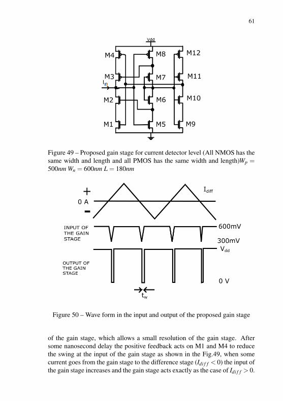
Then if Idi f f = 0 the input remains at some voltage close to Vdd2 . The
gain voltage is designed such a way that when the input of the gain stage isclosed to Vdd
2 the output is goes low level.Fig.50 shows the expected waveform of the proposed current detector
level. One can see that when the current Idi f f = 0 the output switches fromhigh to low level and return to high level when Idi f f 6= 0 after some delay tw,tw represents the delay through the inverter formed by M9-M12. We can seethat the output waveform in Fig.50, is a zero-current level detector. This doesnot represent the real logic of a current comparator. But to form a currentcomparator we can use a flip-flop D in its output.
4.2.1.3 Output stage
The true current comparator logic is Idi f f > 0 the output of the gainstage at high level and when Idi f f < 0 the output of the gain stage at lowlevel. Which is not the same logic with the current level detector in Fig.49.Then to recover the current comparator logic from the gain stage (currentlevel detector) in Fig.49, with output waveform presented in Fig.50. We canuse at the output of the gain stage a simple flip-flop D as shown in FIg.51.
Figure 51 – Flip-Flop D logic
Fig.52 shows the full schematic of the current comparator.Fig.53 shows the input and output waveform of the flip-flop D, when
we have used a flip-flop D in the output of the gain stage to recover a currentcomparator logic. We can see that when the current Idi f f is close to zero,the output of the gain stage of the current level detector (output1) switchesfrom high to low level and if the current Idi f f 6= 0 the output of the gain stage(output1) switches from low to high level. the output (output1) of the gainstage is the input of the flip-flop D. When the output1 Fig.52 goes from highto low, the output of the flip-flop does not change. And some nanosecond,when the output1 goes from low to high the output of the flip-flop changesits state (High-low or low-high). Then using a flip-flop D in the output of thegain stage (current level detector) allows to recover the current comparator

63
Figure 52 – Proposed current comparator
Figure 53 – Output waveform of the proposed current comparator
signal as shown in Fig.53. In resume the proposed gain stage together withthe flip-flop forms a current comparator.
The input of the gain stage rises from low voltage to high voltage(ground to supply voltage). Then we can limit this variation at the input usingtogether to the previous current comparator a current switch system to forma current mode Schmitt trigger where we can reduce the hysteresis width toallow that the input does not rise from high to low voltage.
4.2.2 Current mode Schmitt trigger
In Fig.54, the schematic of the proposed current mode Schmitt triggeris shown. We consider initially that Ms1 is OFF, Ms2 is ON and the input node

64
Figure 54 – Full schematic of the current mode schmitt trigger
voltage of the gain stage is at initial value greater than Vdd/2 and the output ofthe flip-flop is at high level. The current reference is equal to I1 + I2, then we
65
Figure 55 – Waveform of the current mode Schmitt trigger
Figure 56 – Configuration to simulate the current mode Schmitt trigger
Figure 57 – DC simulation of the hysteresis of the current mode Schmitttrigger
consider that the current in the sensor Isens rises from some value below I1+I2.As Isens < I1 + I2 the input node voltage of the gain stage discharge with thecurrent I1+ I2− Isens, when Isens is close to I1+ I2, the input node voltage is atsome voltage below the threshold voltage of the inverter formed by M5 and
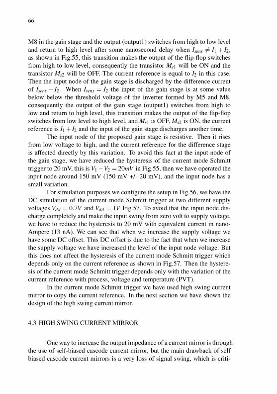
66
M8 in the gain stage and the output (output1) switches from high to low leveland return to high level after some nanosecond delay when Isens 6= I1 + I2,as shown in Fig.55, this transition makes the output of the flip-flop switchesfrom high to low level, consequently the transistor Ms1 will be ON and thetransistor Ms2 will be OFF. The current reference is equal to I2 in this case.Then the input node of the gain stage is discharged by the difference currentof Isens − I2. When Isens = I2 the input of the gain stage is at some valuebelow below the threshold voltage of the inverter formed by M5 and M8,consequently the output of the gain stage (output1) switches from high tolow and return to high level, this transition makes the output of the flip-flopswitches from low level to high level, and Ms1 is OFF, Ms2 is ON, the currentreference is I1 + I2 and the input of the gain stage discharges another time.
The input node of the proposed gain stage is resistive. Then it risesfrom low voltage to high, and the current reference for the difference stageis affected directly by this variation. To avoid this fact at the input node ofthe gain stage, we have reduced the hysteresis of the current mode Schmitttrigger to 20 mV, this is V1−V2 = 20mV in Fig.55, then we have operated theinput node around 150 mV (150 mV +/- 20 mV), and the input node has asmall variation.
For simulation purposes we configure the setup in Fig.56, we have theDC simulation of the current mode Schmitt trigger at two different supplyvoltages Vdd = 0.7V and Vdd = 1V Fig.57. To avoid that the input node dis-charge completely and make the input swing from zero volt to supply voltage,we have to reduce the hysteresis to 20 mV with equivalent current in nano-Ampere (13 nA). We can see that when we increase the supply voltage wehave some DC offset. This DC offset is due to the fact that when we increasethe supply voltage we have increased the level of the input node voltage. Butthis does not affect the hysteresis of the current mode Schmitt trigger whichdepends only on the current reference as shown in Fig.57. Then the hystere-sis of the current mode Schmitt trigger depends only with the variation of thecurrent reference with process, voltage and temperature (PVT).
In the current mode Schmitt trigger we have used high swing currentmirror to copy the current reference. In the next section we have shown thedesign of the high swing current mirror.
4.3 HIGH SWING CURRENT MIRROR
One way to increase the output impedance of a current mirror is throughthe use of self-biased cascode current mirror, but the main drawback of selfbiased cascode current mirrors is a very loss of signal swing, which is criti-

67
Figure 58 – High swing current mirror
cal for low supply voltage. Then to decrease the supply voltage and operateat low voltage we have used the high-swing current mirror [31]. The outputimpedance is given by equation. (4.1). 1.
rout = rDS2b.gm2b.rDS1b (4.1)
The transistor M3 allows to bias properly the source of the transistor M2b atsome value greater than the saturation voltage of M1b.
Then using UCCM (Unified Charge Controlled Model) we have:
Vp3 = φt(√
1+ i f 3−2+ ln(√
1+ i f 3−1)) (4.2)
Vp2 =VS2 +φt(√
1+ i f 2−2+ ln(√
1+ i f 2−1)) (4.3)
We suppose that M3 and M2 are identical transistors, then the samethreshold voltage and the same pinch-off voltage Vp. Then from equations(4.2) and (4.3) we have:
VS2b = φt(F(i f 3)−F(i f 2)) (4.4)
where F(i f i) =√
1+ i f i− 2+ ln(√
1+ i f i− 1). Then to guarantee that thetransistor M1 remains in saturation, we have VSM1 > φt(
√1+ i f 2+3) =VS2b.
From (4.2), (4.3), (4.4) we have:
φt(√
1+ i f 2 +3) = φt(F(i f 3)−F(i f 2)) (4.5)
Transistors M1, M2, M3 have designed in moderate inversion then we have5 = F(i f 3)− F(i f 2). We fix i f 2 = 3 and one can obtain, 5 = F(i f 3) andi f 3 = 26. In this design we chose k = 1, and M1, M2 as identical transistor.Then we have IS1 = IS2 =
IS37 .
1More information about the design of the current mirror is given in [31]

68
To reduce the mismatch, we have to increase the total area [31]. In-creasing so much the width and the length of the transistor reduces the fre-quency transition [31]. Then we have a trade-off between the mismatch andthe frequency transition. This results of the value of the width and length ofM1a, M1b, M2a, M2b and M3 as shown in table4.
Table 4 – Width and length of the high swing current mirror shown in Fig. 58W L
M1a 1 µm x2 L = 3µmM1b 1 µm x2 L = 3µmM2a 1 µm x2 L = 3µmM2b 1 µm x2 L = 3µmM3 1 µm x12 L = 3µm

69
5 MOBILITY-COMPENSATED TIME REFERENCE
Mobility-compensated time reference is a new approach to design atime reference which can be independent with process, voltage and tempera-ture (PVT) variations. This chapter is divided in two parts, the design of themobility-compensated time reference, and the experimental results of the fab-ricated integrated circuit in 180 nm. To design the mobility-compensated timereference generator, we have used a zero-Vt self-biased current source (chap-ter 2), a Voltage controlled current source (chapter 3), and a current modeSchmitt trigger (chapter 4). Measurements of the time reference were takenfor the characterization of the figure of merit (FOM) described in appendixB.
The proposed mobility-compensated time reference is shown in Fig.59.
Figure 59 – Block’s diagram of the proposed time reference
5.1 PRINCIPLE OF THE MOBILITY-COMPENSATED TIME REFERENCE
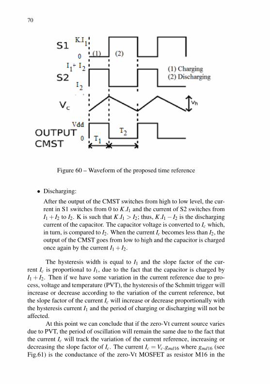
• Charging:
Initially, suppose that the output of the current-mode Schmitt trigger ishigh. In this case, the current through S1 is zero and that through S2 isI1 + I2 Fig.59, thus, the capacitor is charged by the current I1 + I2. Thecapacitor voltage is converted into a current by the voltage-controlledcurrent source (VCCS) Fig.60. The voltage-to current conversion isachieved through MOSFET operating as resistor. This current, Ic, iscompared to I1 + I2. When Ic greater than I1 + I2 the output of theCMST switches from high to low.
70
Figure 60 – Waveform of the proposed time reference
• Discharging:
After the output of the CMST switches from high to low level, the cur-rent in S1 switches from 0 to K.I1 and the current of S2 switches fromI1 + I2 to I2. K is such that K.I1 > I2; thus, K.I1− I2 is the dischargingcurrent of the capacitor. The capacitor voltage is converted to Ic which,in turn, is compared to I2. When the current Ic becomes less than I2, theoutput of the CMST goes from low to high and the capacitor is chargedonce again by the current I1 + I2.
The hysteresis width is equal to I1 and the slope factor of the cur-rent Ic is proportional to I1, due to the fact that the capacitor is charged byI1 + I2. Then if we have some variation in the current reference due to pro-cess, voltage and temperature (PVT), the hysteresis of the Schmitt trigger willincrease or decrease according to the variation of the current reference, butthe slope factor of the current Ic will increase or decrease proportionally withthe hysteresis current I1 and the period of charging or discharging will not beaffected.
At this point we can conclude that if the zero-Vt current source variesdue to PVT, the period of oscillation will remain the same due to the fact thatthe current Ic will track the variation of the current reference, increasing ordecreasing the slope factor of Ic. The current Ic =Vc.gmd16 where gmd16 (seeFig.61) is the conductance of the zero-Vt MOSFET as resistor M16 in the
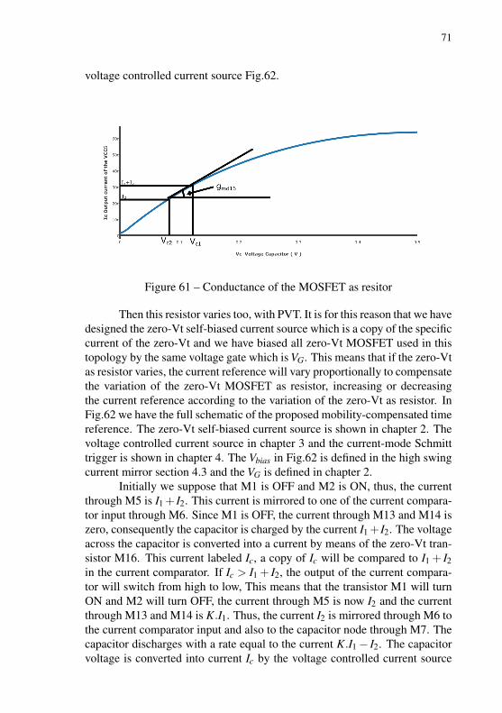
71
voltage controlled current source Fig.62.
Figure 61 – Conductance of the MOSFET as resitor
Then this resistor varies too, with PVT. It is for this reason that we havedesigned the zero-Vt self-biased current source which is a copy of the specificcurrent of the zero-Vt and we have biased all zero-Vt MOSFET used in thistopology by the same voltage gate which is VG. This means that if the zero-Vtas resistor varies, the current reference will vary proportionally to compensatethe variation of the zero-Vt MOSFET as resistor, increasing or decreasingthe current reference according to the variation of the zero-Vt as resistor. InFig.62 we have the full schematic of the proposed mobility-compensated timereference. The zero-Vt self-biased current source is shown in chapter 2. Thevoltage controlled current source in chapter 3 and the current-mode Schmitttrigger is shown in chapter 4. The Vbias in Fig.62 is defined in the high swingcurrent mirror section 4.3 and the VG is defined in chapter 2.
Initially we suppose that M1 is OFF and M2 is ON, thus, the currentthrough M5 is I1 + I2. This current is mirrored to one of the current compara-tor input through M6. Since M1 is OFF, the current through M13 and M14 iszero, consequently the capacitor is charged by the current I1+ I2. The voltageacross the capacitor is converted into a current by means of the zero-Vt tran-sistor M16. This current labeled Ic, a copy of Ic will be compared to I1 + I2in the current comparator. If Ic > I1 + I2, the output of the current compara-tor will switch from high to low, This means that the transistor M1 will turnON and M2 will turn OFF, the current through M5 is now I2 and the currentthrough M13 and M14 is K.I1. Thus, the current I2 is mirrored through M6 tothe current comparator input and also to the capacitor node through M7. Thecapacitor discharges with a rate equal to the current K.I1− I2. The capacitorvoltage is converted into current Ic by the voltage controlled current source

72
Figure 62 – Full schematic of the proposed mobility-compensated time refer-ence

73
and compared to I2. If Ic < I2, the output will switch from low to high.
5.1.1 The MOSFET as a capacitor
Figure 63 – PMOS device as capacitor
The structure of the MOSFET as a capacitor [49], is shown in Fig.63.In our design, the voltage range of the MOSFET that operates as a capacitor iswithin VC1 and VC2 which, in turn, are a function of the charging/dischargingcurrents according to gmd9(VC1−VC2) = I1. The value of the VC1 must be lessthan the saturation voltage of the zero-Vt MOSFET, while the capacitor hasto operates in a linear region, either the accumulation or the inversion region.
We have plotted the graph C- VGB. In our design we have used a PMOStransistor as a capacitor and biased the bulk with the supply voltage, whichis supposed to vary within wide range, from 700mV to 1.8V. We have toguarantee that the capacitor remains in the inversion region, when the supplyvoltage varies. In the range of operation of the supply voltage in our timereference, the MOS capacitor remains in inversion region. Fig.65 shows thevariation of the capacitance with the supply voltage. This simulation was runwith the setup of Fig.64.
Figure 64 – setup for simulation of the non linear capacitor under differentbias bulk level
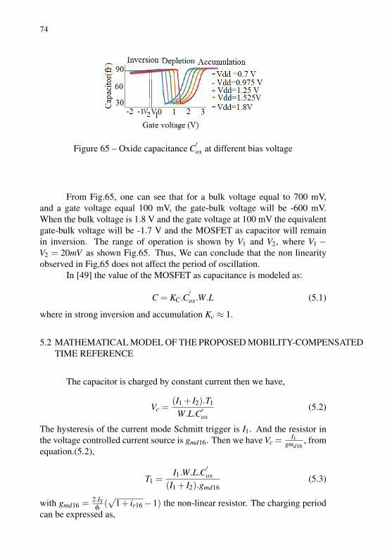
74
Figure 65 – Oxide capacitance C′ox at different bias voltage
From Fig.65, one can see that for a bulk voltage equal to 700 mV,and a gate voltage equal 100 mV, the gate-bulk voltage will be -600 mV.When the bulk voltage is 1.8 V and the gate voltage at 100 mV the equivalentgate-bulk voltage will be -1.7 V and the MOSFET as capacitor will remainin inversion. The range of operation is shown by V1 and V2, where V1 −V2 = 20mV as shown Fig.65. Thus, We can conclude that the non linearityobserved in Fig,65 does not affect the period of oscillation.
In [49] the value of the MOSFET as capacitance is modeled as:
C = KC.C′ox.W.L (5.1)
where in strong inversion and accumulation Kc ≈ 1.
5.2 MATHEMATICAL MODEL OF THE PROPOSED MOBILITY-COMPENSATEDTIME REFERENCE
The capacitor is charged by constant current then we have,
Vc =(I1 + I2).T1
W.L.C′ox(5.2)
The hysteresis of the current mode Schmitt trigger is I1. And the resistor inthe voltage controlled current source is gmd16. Then we have Vc =
I1gmd16
, fromequation.(5.2),
T1 =I1.W.L.C
′ox
(I1 + I2).gmd16(5.3)
with gmd16 =2.ISφt
(√
1+ ir16−1) the non-linear resistor. The charging periodcan be expressed as,
75
T1 =I1.W.L.C
′ox
(I1 + I2).2.ISφt
(√
1+ ir16−1)(5.4)
where IS = W2.L µnn.C
′oxφ 2
t is the specific current of the zero-Vt MOSFET asresitor. The charging period is given by,
T1 =I1.W.L.C
′ox
(I1 + I2).(WL µnn.C′oxφt)(
√1+ ir16−1)
(5.5)
One can observe that the oscillation period is independent of the oxide capac-itance. The period oscillation is given by:
T0 = T1 +T2 (5.6)
where T1 =T2D , T2 is the discharging period as shown in Fig.60. D is the duty
cycle. This duty cycle is given by D = I1+I2K.I1−I2
.
T0 = T1(D+1) =(D+1)I1.L
(I1 + I2).(1L µnn.φt)(
√1+ ir16−1)
(5.7)
After some simplification one can come to the result of the frequency of os-cillation,
f0 = [(K.I1− I2)(I1 + I2)(n(
√1+ ir16−1))
I21 (K +1).L2 ].µn.φt (5.8)
Then we can simplify the frequency of oscillation in two terms, the de-sign parameter A = (K.I1−I2)(I1+I2)(n(
√1+ir16−1))
I21 (K+1).L2 and the technology parameter
µn.φt . And the frequency of oscillation can be reduced to.
f0 = A.µn.φt (5.9)
In chapter 2 we have proved that the inversion level of the transistor M2zvt inthe zero-Vt self-biased current source is constant with respect to process andtemperature variations due to the fact that it is a specific current extractor,then as the transistor zero-Vt M17 used as resistor in the voltage controlledcurrent source is biased by the same voltage gate VG of the transistor M1zvt
and M2zvt , Fig.30, one can consider that the reverse inversion level of thetransistor M16 in Fig.62 is more or less constant and ir16 ≈ i f 2zvt ≈ ir1zvt .i f 2zvt and ir1zvt represent the forward inversion and the reverse inversion levelof M2 and M1 respectively in Fig.30. Therefore the design parameter ’A’ is

76
also independent with process and temperature variations, since we considerthat the slope factor is independent with temperature variation.
f0 = [(K.I1− I2)(I1 + I2)(n(
√1+ i f 2zvt −1))
I21 (K +1).L2 ].µn.φt (5.10)
The variation of the frequency with respect to temperature is,
δ f0
δT= A(
kq.µn +φt .
δ µn
δT) (5.11)
in chapter 1 we have given some theory about the mobility variationwith respect to temperature variation and we can resume that the surface mo-bility in MOSFET device can be approximated to the mobility of the bulk inhigh temperature and low field. the bulk mobility is defined as µn = µ0(
TT0)−β
where β is a constant(chapter 1).After some manipulation of equation(5.11), we have,
δ f0/ f0
δT=
(1−β )
T(5.12)
From equation.(5.12) we can interpret that if β = 1 the frequency f0will be independent of temperature variation. The percent variation of the fre-quency with respect to temperature is independent of frequency. From equa-tion.(5.12) we can interpret too, that at high temperature the percent variationof the frequency is very small.
5.3 SIMULATION RESULTS
Fig.66 shows the layout of the proposed mobility-compensated timereference, where the total area is approximately 0.01 mm2. without outputbuffer.
Fig.67 shows the output simulation of the mobility-compensated timereference and Fig.68, shows the layout and the bonding diagram of the chip.The triangular waveform is the output of the capacitor. The output of theCMST shows the width of the hysteresis, which is close to 25 mV in simula-tion. The period of oscillation is close to 32 kHz. The Monte Carlo simulationfor 247 samples resulted in the histogram shown in Fig.69 with a mean valueof 32,5 kHz and a standard deviation of 2.33 kHz. This standard deviation isdue to the mismatch in the current mirror and differential pair.
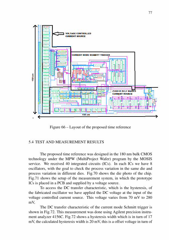
77
Figure 66 – Layout of the proposed time reference
5.4 TEST AND MEASUREMENT RESULTS
The proposed time reference was designed in the 180 nm bulk CMOStechnology under the MPW (MultiProject Wafer) program by the MOSISservice. We received 40 integrated circuits (ICs). In each ICs we have 8oscillators, with the goal to check the process variation in the same die andprocess variation in different dies. Fig.70 shows the die photo of the chip.Fig.71 shows the setup of the measurement system, in which the prototypeICs is placed in a PCB and supplied by a voltage source.
To access the DC transfer characteristic, which is the hysteresis, ofthe fabricated oscillator we have applied the DC voltage at the input of thevoltage controlled current source. This voltage varies from 70 mV to 280mV,
The DC transfer characteristic of the current mode Schmitt trigger isshown in Fig.72. This measurement was done using Agilent precision instru-ment analyzer 4156C. Fig.72 shows a hysteresis width which is in turn of 17mV, the calculated hysteresis width is 20 mV, this is a offset voltage in turn of

78
Figure 67 – Simulation result of the proposed time reference : the triangularwaveform is the capacitor voltage and rectangular wave form is the output ofthe CMST, for Vdd = 1 V Temp = 27◦C
3 mV, this offset voltage is due to mismatch in differential pair and/or currentmirror.
We have tested a total of 280 circuits (8 circuits in 35 ICs). The rangeof the output frequency was from 29 kHz to 34kHz. Fig.73 shows the fre-quency variation versus percentage of the total number of tested oscillatorwith a supply voltage of 1 V. From this figure one can observe that more than20% of all the tested oscillators are accurate. The lower value of frequency is
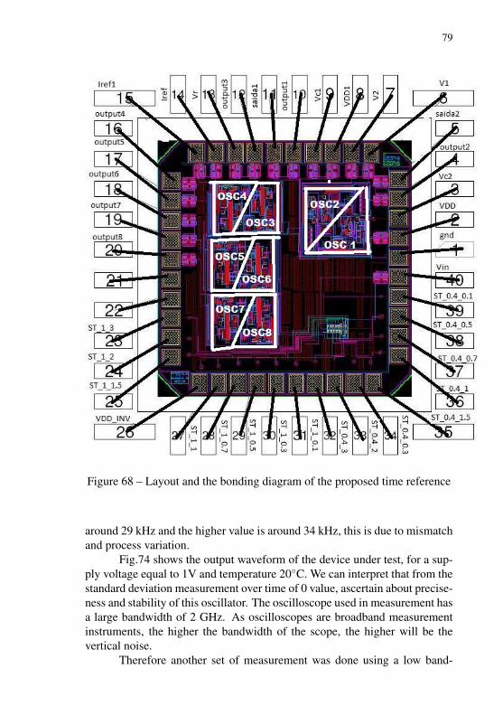
79
Figure 68 – Layout and the bonding diagram of the proposed time reference
around 29 kHz and the higher value is around 34 kHz, this is due to mismatchand process variation.
Fig.74 shows the output waveform of the device under test, for a sup-ply voltage equal to 1V and temperature 20◦C. We can interpret that from thestandard deviation measurement over time of 0 value, ascertain about precise-ness and stability of this oscillator. The oscilloscope used in measurement hasa large bandwidth of 2 GHz. As oscilloscopes are broadband measurementinstruments, the higher the bandwidth of the scope, the higher will be thevertical noise.
Therefore another set of measurement was done using a low band-

80
Figure 69 – Monte Carlo Simulation for the proposed mobility-compensatedtime reference
Figure 70 – Die photo of the time reference
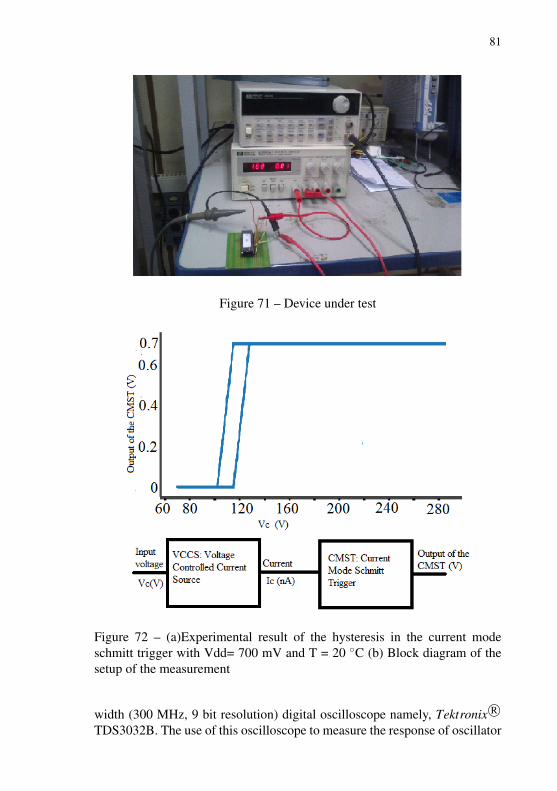
81
Figure 71 – Device under test
Figure 72 – (a)Experimental result of the hysteresis in the current modeschmitt trigger with Vdd= 700 mV and T = 20 ◦C (b) Block diagram of thesetup of the measurement
width (300 MHz, 9 bit resolution) digital oscilloscope namely, Tektronix R©TDS3032B. The use of this oscilloscope to measure the response of oscillator
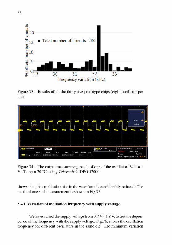
82
Figure 73 – Results of all the thirty five prototype chips (eight oscillator perdie)
Figure 74 – The output measurement result of one of the oscillator. Vdd = 1V , Temp = 20 ◦C, using Tektronix R© DPO 52000.
shows that, the amplitude noise in the waveform is considerably reduced. Theresult of one such measurement is shown in Fig.75.
5.4.1 Variation of oscillation frequency with supply voltage
We have varied the supply voltage from 0.7 V - 1.8 V, to test the depen-dence of the frequency with the supply voltage. Fig.76, shows the oscillationfrequency for different oscillators in the same die. The minimum variation
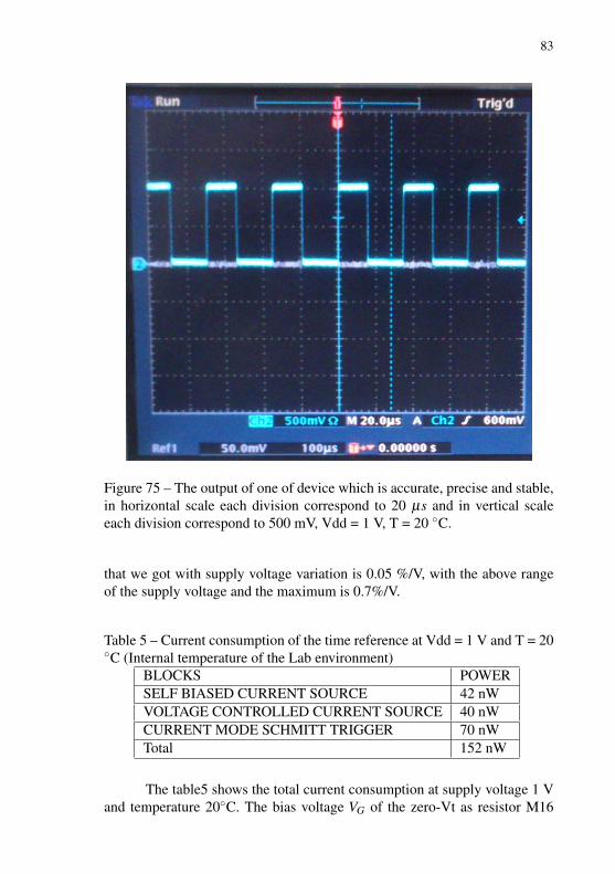
83
Figure 75 – The output of one of device which is accurate, precise and stable,in horizontal scale each division correspond to 20 µs and in vertical scaleeach division correspond to 500 mV, Vdd = 1 V, T = 20 ◦C.
that we got with supply voltage variation is 0.05 %/V, with the above rangeof the supply voltage and the maximum is 0.7%/V.
Table 5 – Current consumption of the time reference at Vdd = 1 V and T = 20◦C (Internal temperature of the Lab environment)
BLOCKS POWERSELF BIASED CURRENT SOURCE 42 nWVOLTAGE CONTROLLED CURRENT SOURCE 40 nWCURRENT MODE SCHMITT TRIGGER 70 nWTotal 152 nW
The table5 shows the total current consumption at supply voltage 1 Vand temperature 20◦C. The bias voltage VG of the zero-Vt as resistor M16

84
Figure 76 – Result of the supply voltage variation from 700 mV to 1.8V forall height circuits in one die,(each die contains height relaxations oscillators)
in Fig.62 varies with the supply voltage. This means that at different supplyvoltage the equivalent transconductance of the transistor M16 could vary andthis affects the oscillation period. This is the main reason of the variationof the oscillation with the supply voltage. But this variation is in turn on0.1 % and present in simulation a total variation of the oscillation period of0.02%/V. In test and measurement result we got a total variation of 0.05%/Vfor the good case and the worst case 0.7%/V.
5.4.2 Temperature variation
To test the oscillator response with respect to (i.e., w.r.t) temperature,we have varied the temperature from -20 ◦C to 80 ◦C. This test was doneusing a thermal chamber, and the response was observed on an oscilloscope.Throughout the test we have used a supply voltage of 1 V; the setup is shownin Fig.77. The variation of frequency response w.r.t., temperature is shown inFig.78. We tested 5 oscillators from different dies. The minimum variation inthe range of -20 ◦C to 80 ◦C, is around 30 ppm/◦C and the maximum variationis 90 ppm/◦C. At temperatures > 40◦C, the frequency is stable with respectto temperature variation.
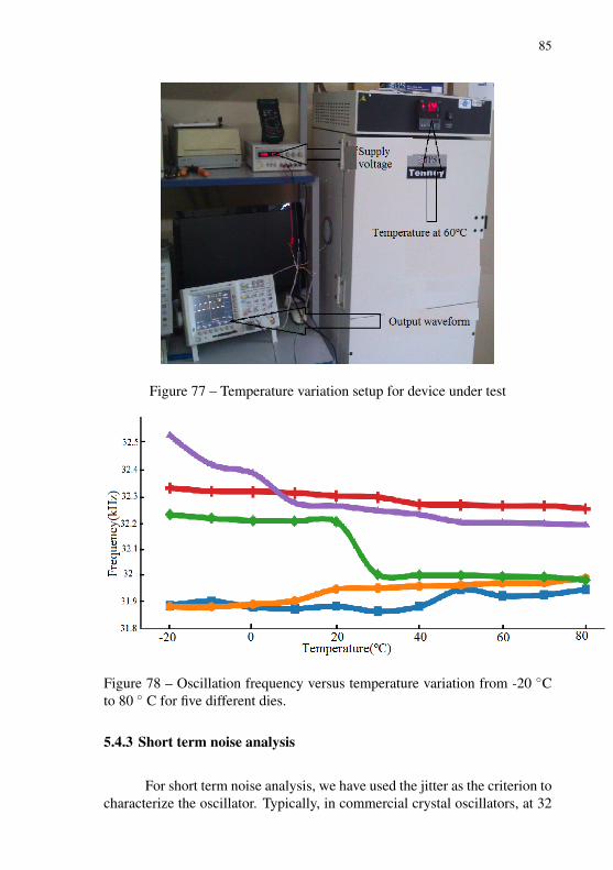
85
Figure 77 – Temperature variation setup for device under test
Figure 78 – Oscillation frequency versus temperature variation from -20 ◦Cto 80 ◦ C for five different dies.
5.4.3 Short term noise analysis
For short term noise analysis, we have used the jitter as the criterion tocharacterize the oscillator. Typically, in commercial crystal oscillators, at 32
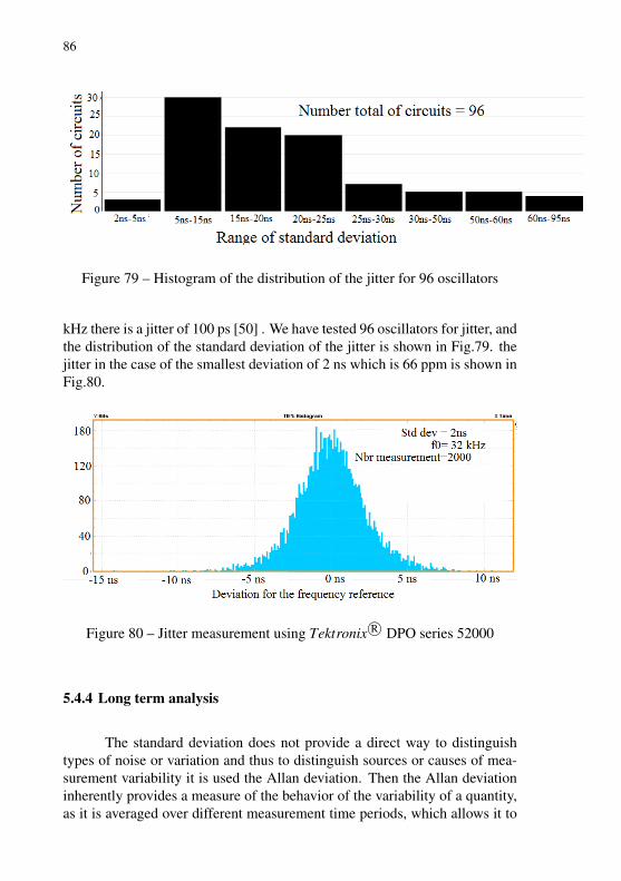
86
Figure 79 – Histogram of the distribution of the jitter for 96 oscillators
kHz there is a jitter of 100 ps [50] . We have tested 96 oscillators for jitter, andthe distribution of the standard deviation of the jitter is shown in Fig.79. thejitter in the case of the smallest deviation of 2 ns which is 66 ppm is shown inFig.80.
Figure 80 – Jitter measurement using Tektronix R© DPO series 52000
5.4.4 Long term analysis
The standard deviation does not provide a direct way to distinguishtypes of noise or variation and thus to distinguish sources or causes of mea-surement variability it is used the Allan deviation. Then the Allan deviationinherently provides a measure of the behavior of the variability of a quantity,as it is averaged over different measurement time periods, which allows it to
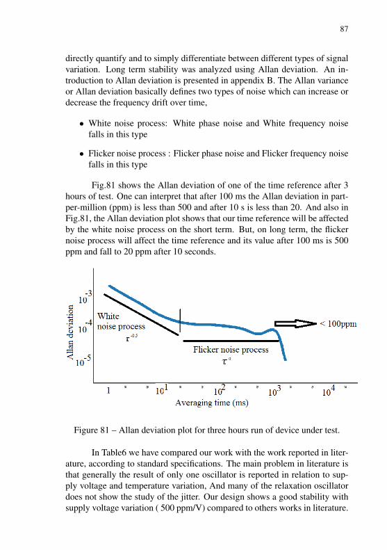
87
directly quantify and to simply differentiate between different types of signalvariation. Long term stability was analyzed using Allan deviation. An in-troduction to Allan deviation is presented in appendix B. The Allan varianceor Allan deviation basically defines two types of noise which can increase ordecrease the frequency drift over time,
• White noise process: White phase noise and White frequency noisefalls in this type
• Flicker noise process : Flicker phase noise and Flicker frequency noisefalls in this type
Fig.81 shows the Allan deviation of one of the time reference after 3hours of test. One can interpret that after 100 ms the Allan deviation in part-per-million (ppm) is less than 500 and after 10 s is less than 20. And also inFig.81, the Allan deviation plot shows that our time reference will be affectedby the white noise process on the short term. But, on long term, the flickernoise process will affect the time reference and its value after 100 ms is 500ppm and fall to 20 ppm after 10 seconds.
Figure 81 – Allan deviation plot for three hours run of device under test.
In Table6 we have compared our work with the work reported in liter-ature, according to standard specifications. The main problem in literature isthat generally the result of only one oscillator is reported in relation to sup-ply voltage and temperature variation, And many of the relaxation oscillatordoes not show the study of the jitter. Our design shows a good stability withsupply voltage variation ( 500 ppm/V) compared to others works in literature.
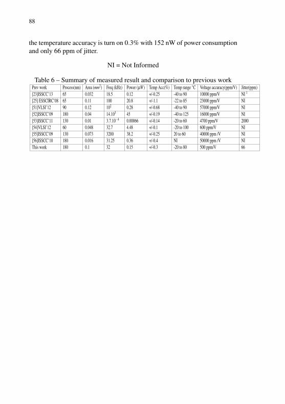
88
the temperature accuracy is turn on 0.3% with 152 nW of power consumptionand only 66 ppm of jitter.
NI = Not Informed
Table 6 – Summary of measured result and comparison to previous workPrev work Process(nm) Area (mm2) Freq (kHz) Power (µW ) Temp Acc(%) Temp range ◦C Voltage accuracy(ppm/V) Jitter(ppm)[23]ISSCC’13 65 0.032 18.5 0.12 +/-0.25 -40 to 90 10000 ppm/V NI 1
[25] ESSCIRC’08 65 0.11 100 20.8 +/-1.1 -22 to 85 23000 ppm/V NI[51]VLSI’12 90 0.12 102 0.28 +/-0.68 -40 to 90 57000 ppm/V NI[52]ISSCC’09 180 0.04 14.103 45 +/-0.19 -40 to 125 16000 ppm/V NI[53]ISSCC’11 130 0.01 3.7.10−4 0.00066 +/-0.14 -20 to 60 4700 ppm/V 2000[54]VLSI’12 60 0.048 32.7 4.48 +/-0.1 -20 to 100 600 ppm/V NI[55]ISSCC’09 130 0.073 3200 38.2 +/-0.25 20 to 60 40000 ppm /V NI[56]ISSCC’10 180 0.016 31.25 0.36 +/-0.4 NI 50000 ppm /V NIThis work 180 0.1 32 0.15 +/-0.3 -20 to 80 500 ppm/V 66
89
6 CONCLUSION
This final chapter presents a summary of the main findings of thiswork and a short overview of the possible applications and research topicsoriginating from this work that could be investigated in the future.
6.1 MAIN RESULT
• Low-doping MOSFET used as resistor shows a small variation withprocess and temperature variation when compensated by thermal volt-age, compared to a standard MOSFET. In the proposed time referencethe use of the zero-Vt self-biased current source allows to generatesome current source which in turn has the same PVT variation withthe zero-Vt MOSFET used as resistor. This allows that we can trackthe variation of the MOSFET as resistor. Thus, the variation of zero-Vtas resistor does not affect our time reference.
• Mobility-Compensated time reference can be used as time referencein some range of temperature (30 ppm /◦C) and wide range of supplyvoltage with 66 ppm of Jitter. At high temperature (Temp≥ 27 ◦C), theproposed time reference is stable and precise, due to the fact that themobility is stable at high temperature. The long term study with Allanvariance shows some 500 ppm variation due to white noise process atlong term. Thus, the proposed time reference could be used in place ofcrystal oscillators in applications where only precision and stability arerequired(e.g Clock for power management).
• Used a current comparator, instead of voltage comparator in relaxationoscillator, can allow to track the PVT variation of the current referenceand consequently produce more stable frequency, and achieve someprecise time reference.
6.2 FUTURE WORK
We can improve the performance of the relaxation oscillator in relationto mismatch, temperature and jitter. To increase the performance in relationto mismatch we have to increase the total area in the voltage controlled cur-rent source and the high swing current mirror. To increase the performance inrelation to the short term stability, it will be necessary to increase the power

90
consumption, this will reduce the jitter. One problem in the design of therelaxation oscillator using a current comparator, is that he has a few publica-tions of current comparator with good performance in literature. Then, it isnecessary to improve the topology of the current comparator to achieve, highspeed and small input current resolution, which can work also at low supplyvoltage without a dead zone.
APPENDIX A -- Advanced Compact Model


93
Main equation using Advanced Compact Model (ACM):
ID = IF − IR (A.1)
ID is the drain-source current, IF is the forward current and IR is thereverse current.
IF = IS.i f (A.2)
IR = IS.ir (A.3)
IS is the specific current, i f is the forward inversion level, ir is thereverse inversion level.
ID = IS(i f − ir) (A.4)
Unified Charge Control Model (UCCM)
Vpi−Vsbi = φt(√
1+ i f i−2+ ln(√
1+ i f i−1)) (A.5)
Vpi−Vdbi = φt(√
1+ iri−2+ ln(√
1+ iri−1)) (A.6)
where Vpi =Vgbi−Vth
n is the pinch-off voltage, Vth is the threshold volt-age. n is the slope factor.
gms =2.IS
φt(√
1+ i f i−1)) (A.7)
gmr =2.IS
φt(√
1+ iri−1)) (A.8)
gms and gmr are transconductance related to the source and the drainrespectively.

94
APPENDIX B -- Figure of Merit of the oscillator as time reference


97
B.1 FIGURE OF MERIT
Figure 82 – Illustration of Precision-Stability-Accuracy
The FOM used in this work is divided in, 1 Accuracy, 2 Stability, 3Precision. Fig.82 illustrates the accuracy, precision and stability that we willdiscuss in the next section.
B.1.1 Accuracy
Accuracy is the degree of conformity of a measured or calculated valueto its definition. Accuracy is also related with the offset from an ideal value.For example, a time offset is the difference between a measured on-time pulseand an ideal on-time pulse. Frequency offset is the difference between a mea-sured frequency and an ideal frequency with zero uncertainty as shown inequation.B.1. This ideal frequency is called the nominal frequency. In thiswork this nominal value is 32 kHz.
fo f f set =fmeasured− fnominal
fnominal(B.1)

98
This frequency offset is defined in part-per million this is
α = fo f f setx106(ppm) (B.2)
B.1.2 Precision
Precision is the random uncertainty of a measured value, expressed bythe standard deviation or by a multiple of the standard deviation. Then wecan say that the accuracy is the closeness of the agreement between the resultof a measurement and a true value.
B.1.3 Stability
Stability indicates how well an oscillator can produce the same timeor frequency offset over a given time interval, it doesn’t indicate whetherthe time or frequency is “right” or “wrong”. Stability and accuracy are twodifferent terms because, accuracy indicates how well an oscillator has been seton time or on frequency. To understand this difference, consider that a stableoscillator that needs adjustment might produce a frequency with a large offset.Or an unstable oscillator that was just adjusted might temporarily producea frequency near its nominal value. Fig.82 shows the relationship betweenaccuracy and stability.
Stability can be divided into: 1. Short-term stability that refers tofluctuations over intervals less than 100 s. and 2. Long-term stability usuallyrefers to measurement intervals greater than 100 s, but for robust behavior itshould be greater than 1 day for an oscillator [57].
Mathematically stability is defined as the statistical estimate of thefrequency or time fluctuations of a signal over a given time interval. Thesefluctuations are measured with respect to a mean frequency or time offset asshown in equation.(B.1). Stability estimates can be made in either the fre-quency domain or time domain, and can be calculated from a set of eitherfrequency offset or time interval measurements. In some fields of measure-ment, stability is estimated by taking the standard deviation of the data set.However, standard deviation only works with stationary data, where the re-sults are time independent, and the noise is white, meaning that it is evenlydistributed across the frequency band of the measurement. Oscillator data isusually non-stationary, since it contains time dependent noise contributed bythe frequency offset. With the stationary data, the mean and standard devi-ation will converge to a particular value. As more measurements are made

99
with non-stationary data, the mean and standard deviation never converge toany particular value. Instead, there is a moving mean that changes each timewe add a measurement. For these reasons, a non-classical statistic like Allanvariance can be used to estimate long term stability in the time domain. TheAllan variance is a two-sample variance formed by the average of the squareddifferences between successive values of a regularly measured quantity takenover sampling periods from the measuring interval up to half the maximummeasurement time. But since it is the square root of the variance, its propername is the Allan deviation. The equation of Allan deviation is,
σ f (τ) =
√1
2.(M−1)Σ
M−1i=1 ( fi+1− fi)2 (B.3)
M is the number of sample and fi is the frequency at the time τi. Thestability is again divided in two parts: long term stability and short term sta-bility.
Also, standard deviation does not provide a direct way to distinguishtypes of noise or variation, and thus to distinguish sources or causes of mea-surement variability, we can use the Allan deviation. Because Allan deviationcan measure the behavior of the variability of a quantity over different mea-surements of time period, which allows it to directly quantify and differentiatebetween different types of signal variation, [57], [58].

100

101
LIST OF FIGURES
Figure 1 Example of use of xtal oscillator in cell phone [3] . . . . . . . . . . . 15Figure 2 Wien Bridge Oscillator [4] . . . . . . . . . . . . . . . . . . . . . . . . . . . . . . . . 16Figure 3 Crystal Oscillator . . . . . . . . . . . . . . . . . . . . . . . . . . . . . . . . . . . . . . . . 16Figure 4 Cuts of the crystal resonator [5] . . . . . . . . . . . . . . . . . . . . . . . . . . . 17Figure 5 Equivalent circuit of the crystal oscillator [6] . . . . . . . . . . . . . . . 17Figure 6 The reactance of the crystal varies with the frequency of oper-ation near resonance [5] . . . . . . . . . . . . . . . . . . . . . . . . . . . . . . . . . . . . . . . . . . . . 18Figure 7 (a) Series resonant oscillator (b) Parellel resonant circuit [5] . 18Figure 8 Crystal with temperature variation at different fabrication pro-cess [5] . . . . . . . . . . . . . . . . . . . . . . . . . . . . . . . . . . . . . . . . . . . . . . . . . . . . . . . . . . . 19Figure 9 Aging of crystal resonator over time [6] . . . . . . . . . . . . . . . . . . . . 20Figure 10 (a) Generic LC Oscillator Block diagram (b) Typical CMOSimplementation (bias not shown) . . . . . . . . . . . . . . . . . . . . . . . . . . . . . . . . . . . . 22Figure 11 Amplifier in close loop . . . . . . . . . . . . . . . . . . . . . . . . . . . . . . . . . . . 24Figure 12 Current-starved ring oscillator . . . . . . . . . . . . . . . . . . . . . . . . . . . . 24Figure 13 RC + Ring Oscillator [20] . . . . . . . . . . . . . . . . . . . . . . . . . . . . . . . . 25Figure 14 Relaxation oscillator with 2 comparators [21] . . . . . . . . . . . . . . . 26Figure 15 Relaxation Oscillator using one comparator only [22] . . . . . . . 27Figure 16 Relaxation oscillator with one comparator and compensatedOffset [23] . . . . . . . . . . . . . . . . . . . . . . . . . . . . . . . . . . . . . . . . . . . . . . . . . . . . . . . . 27Figure 17 Current mode relaxation oscillator [24] . . . . . . . . . . . . . . . . . . . . 28Figure 18 Mobility-based time reference [25] . . . . . . . . . . . . . . . . . . . . . . . . 28Figure 19 Waveform of the mobility-based time reference [25] . . . . . . . . 29Figure 20 Differents models of the mobility used in electrical simulator 30Figure 21 Predominant factor on surface mobility in different conditions 31Figure 22 : Bulk mobility variation with temperature at different dopinglevels . . . . . . . . . . . . . . . . . . . . . . . . . . . . . . . . . . . . . . . . . . . . . . . . . . . . . . . . . . . . . 33Figure 23 Bulk mobility versus doping level . . . . . . . . . . . . . . . . . . . . . . . . . 34Figure 24 Set-up to extract the mobility with respect to temperature vari-ation for the zero-Vt MOSFET in 180 nm . . . . . . . . . . . . . . . . . . . . . . . . . . . 34Figure 25 Simulation result of the mobility with temperature in zero-VtMOSFET device . . . . . . . . . . . . . . . . . . . . . . . . . . . . . . . . . . . . . . . . . . . . . . . . . . 35Figure 26 Block’s diagram of the proposed time reference . . . . . . . . . . . . . 37

102
Figure 27 Full schematic of the self-biased current source . . . . . . . . . . . . . 39Figure 28 Voltage following current mirror . . . . . . . . . . . . . . . . . . . . . . . . . . 40Figure 29 Specific current generator block . . . . . . . . . . . . . . . . . . . . . . . . . . . 41Figure 30 Proposed zero-Vt specific current generator . . . . . . . . . . . . . . . . 42Figure 31 Zero-Vt specific current generator vs temperature (◦C) . . . . . . 45Figure 32 Simulation Zero-Vt specific current generator vs supply volt-age . . . . . . . . . . . . . . . . . . . . . . . . . . . . . . . . . . . . . . . . . . . . . . . . . . . . . . . . . . . . . . . 45Figure 33 Operational transconductance amplifier . . . . . . . . . . . . . . . . . . . . 47Figure 34 Common source amplifier . . . . . . . . . . . . . . . . . . . . . . . . . . . . . . . . 48Figure 35 Common source amplifier with load . . . . . . . . . . . . . . . . . . . . . . . 49Figure 36 Common source amplifier with load and degeneration . . . . . . . 49Figure 37 (a)NMOS common source amplifier with diode connected load(b) PMOS common source amplifier with NMOS load in triode . . . . . . . . 50Figure 38 Schematic of the voltage controlled current source block. . . . . 50Figure 39 Schematic of the voltage controlled current source block. . . . . 51Figure 40 Voltage controlled current source (the capacitor C is for overallstability) . . . . . . . . . . . . . . . . . . . . . . . . . . . . . . . . . . . . . . . . . . . . . . . . . . . . . . . . . . 51Figure 41 Setup to plot the output characteristic of the zero-Vt (IdvsVds) 53Figure 42 Freita’s comparator [35] . . . . . . . . . . . . . . . . . . . . . . . . . . . . . . . . . . 55Figure 43 Traff’s comparator [36] . . . . . . . . . . . . . . . . . . . . . . . . . . . . . . . . . . 55Figure 44 Class AB current comparator with switch [43] . . . . . . . . . . . . . . 56Figure 45 Class AB current comparator with compensation circuit [44] . 57Figure 46 Toumazou’s current comparator [45] . . . . . . . . . . . . . . . . . . . . . . . 59Figure 47 Waveform from toumazou current comparator . . . . . . . . . . . . . . 59Figure 48 General topology of current comparator . . . . . . . . . . . . . . . . . . . . 60Figure 49 Proposed gain stage for current detector level (All NMOShas the same width and length and all PMOS has the same width andlength)Wp = 500nm Wn = 600nm L = 180nm . . . . . . . . . . . . . . . . . . . . . . . . . 61Figure 50 Wave form in the input and output of the proposed gain stage 61Figure 51 Flip-Flop D logic . . . . . . . . . . . . . . . . . . . . . . . . . . . . . . . . . . . . . . . . 62Figure 52 Proposed current comparator . . . . . . . . . . . . . . . . . . . . . . . . . . . . . . 63Figure 53 Output waveform of the proposed current comparator . . . . . . . 63Figure 54 Full schematic of the current mode schmitt trigger . . . . . . . . . . 64Figure 55 Waveform of the current mode Schmitt trigger . . . . . . . . . . . . . . 65Figure 56 Configuration to simulate the current mode Schmitt trigger . . 65
103
Figure 57 DC simulation of the hysteresis of the current mode Schmitttrigger . . . . . . . . . . . . . . . . . . . . . . . . . . . . . . . . . . . . . . . . . . . . . . . . . . . . . . . . . . . . 65Figure 58 High swing current mirror . . . . . . . . . . . . . . . . . . . . . . . . . . . . . . . . 67Figure 59 Block’s diagram of the proposed time reference . . . . . . . . . . . . . 69Figure 60 Waveform of the proposed time reference . . . . . . . . . . . . . . . . . . 70Figure 61 Conductance of the MOSFET as resitor . . . . . . . . . . . . . . . . . . . . 71Figure 62 Full schematic of the proposed mobility-compensated time ref-erence . . . . . . . . . . . . . . . . . . . . . . . . . . . . . . . . . . . . . . . . . . . . . . . . . . . . . . . . . . . . 72Figure 63 PMOS device as capacitor . . . . . . . . . . . . . . . . . . . . . . . . . . . . . . . . 73Figure 64 setup for simulation of the non linear capacitor under differentbias bulk level . . . . . . . . . . . . . . . . . . . . . . . . . . . . . . . . . . . . . . . . . . . . . . . . . . . . . 73Figure 65 Oxide capacitance C
′ox at different bias voltage . . . . . . . . . . . . . . 74
Figure 66 Layout of the proposed time reference . . . . . . . . . . . . . . . . . . . . . 77Figure 67 Simulation result of the proposed time reference : the trian-gular waveform is the capacitor voltage and rectangular wave form is theoutput of the CMST, for Vdd = 1 V Temp = 27◦C . . . . . . . . . . . . . . . . . . . . . 78Figure 68 Layout and the bonding diagram of the proposed time refer-ence . . . . . . . . . . . . . . . . . . . . . . . . . . . . . . . . . . . . . . . . . . . . . . . . . . . . . . . . . . . . . . 79Figure 69 Monte Carlo Simulation for the proposed mobility-compensatedtime reference . . . . . . . . . . . . . . . . . . . . . . . . . . . . . . . . . . . . . . . . . . . . . . . . . . . . . 80Figure 70 Die photo of the time reference . . . . . . . . . . . . . . . . . . . . . . . . . . . 80Figure 71 Device under test . . . . . . . . . . . . . . . . . . . . . . . . . . . . . . . . . . . . . . . . 81Figure 72 (a)Experimental result of the hysteresis in the current modeschmitt trigger with Vdd= 700 mV and T = 20 ◦C (b) Block diagram ofthe setup of the measurement . . . . . . . . . . . . . . . . . . . . . . . . . . . . . . . . . . . . . . . 81Figure 73 Results of all the thirty five prototype chips (eight oscillatorper die) . . . . . . . . . . . . . . . . . . . . . . . . . . . . . . . . . . . . . . . . . . . . . . . . . . . . . . . . . . . 82Figure 74 The output measurement result of one of the oscillator. Vdd =1 V , Temp = 20 ◦C, using Tektronix R© DPO 52000. . . . . . . . . . . . . . . . . . . 82Figure 75 The output of one of device which is accurate, precise and sta-ble, in horizontal scale each division correspond to 20 µs and in verticalscale each division correspond to 500 mV, Vdd = 1 V, T = 20 ◦C. . . . . . . . 83Figure 76 Result of the supply voltage variation from 700 mV to 1.8Vfor all height circuits in one die,(each die contains height relaxations os-cillators) . . . . . . . . . . . . . . . . . . . . . . . . . . . . . . . . . . . . . . . . . . . . . . . . . . . . . . . . . 84Figure 77 Temperature variation setup for device under test . . . . . . . . . . . 85Figure 78 Oscillation frequency versus temperature variation from -20
104
◦C to 80 ◦ C for five different dies. . . . . . . . . . . . . . . . . . . . . . . . . . . . . . . . . . . 85Figure 79 Histogram of the distribution of the jitter for 96 oscillators . . . 86Figure 80 Jitter measurement using Tektronix R© DPO series 52000 . . . . 86Figure 81 Allan deviation plot for three hours run of device under test. . 87Figure 82 Illustration of Precision-Stability-Accuracy. . . . . . . . . . . . . . . . . 97
105
LIST OF TABLES
Table 1 Comparison between techniques to generate time references . . 36Table 2 Width and length of the zero-Vt Self-Biased current source . . . 44Table 3 Width and length of the voltage controlled current source . . . . 53Table 4 Width and length of the high swing current mirror shown in Fig.58. . . . . . . . . . . . . . . . . . . . . . . . . . . . . . . . . . . . . . . . . . . . . . . . . . . . . . . . . . . . . . . . 68Table 5 Current consumption of the time reference at Vdd = 1 V and T= 20 ◦C (Internal temperature of the Lab environment) . . . . . . . . . . . . . . . . 83Table 6 Summary of measured result and comparison to previous work 88

106

REFERÊNCIAS BIBLIOGRÁFICAS
1 L. Han and N. Hua, “A Distributed Time Synchronization Solutionwithout Satellite Time Reference for Mobile Communication”, IEEECommunications Letters, vol. 17, no. 7, pp. 1447 - 1450, Jul. 2013.
2 J.-L. Ferrant, M. Gilson, S. Jobert, M. Mayer, L. Montini, M. Ouel-lette, S. Rodrigues, and S. Ruffini, “Synchronous Ethernet and IEEE1588 in Telecoms”, May 2013.
3 mccorquodale, “CMOS challenge quartz”,21-Mar-2006. [Online]. Available:www.ewh.ieee.org/r7/toronto/chapters/ssc/mccorquodaleUToronto09.pd f .[Accessed: 26-Oct-2015]
4 K. Clarke, “Wien bridge oscillator design”, Proceedings of the IRE,vol. 41, no. 2, pp. 246 - 249, Feb. 1953.
5 ”CrystalOscillators.pdf”,[Online]. Available: htt p : //kunz −pc.sce.carleton.ca/thesis/CrystalOscillators.pd f . [Accessed:28-Oct-2015].
6 Jauch Quartz GmbH, “Quartz Crystal Theory”, www.jauch.de/. [On-line]. [Accessed: 28-Oct-2015].
7 CITIZEN FINETECH MIYOTA CO., “Cutting directionand frequency Temperature characteristics, CITIZEN FI-NETECH MIYOTA CO.,LTD.” [Online]. Available: htt p ://c f m.citizen.co. jp/english/product/cvocharacter.html. [Ac-cessed: 09-Oct-2015].
8 MICAS, “Crystal oscillator design”, http://iroi.seu.edu.cn, 2008. [On-line]. Available: http://iroi.seu.edu.cn/teachers/chym/analog/22.pdf.[Accessed: 12-Oct-2015].
9 “Fastest Wireless On-ramp to the Internet of Things”, 10-Aug-2015. [Online]. Available: http://www.silabs.com. [Accessed: 09-Oct-2015].
10 H. C. Nathanson and R. A. Wickstrom, “A resonant-gate silicon sur-face transistor with high-Q band-pass properties”, Applied PhysicsLetters, vol. 7, no. 4, p. 84, 1965.
108 Referências Bibliográficas
11 M. Sadiku, “MEMS”, IEEE Potentials, vol. 21, no. 1, pp. 4-5, 2002.
12 S. Tabatabaei and A. Partridge, “Silicon MEMS Oscillators for High-Speed Digital Systems”, IEEE Micro, vol. 30, no. 2, pp. 80?89, Mar.2010.
13 Si-Time, “MEMS replacing Quartz oscillator Application note”, 2009.[Online]. Available: www.sitime.com. [Accessed: 02-Oct-2015].
14 M. Lutz, A. Partridge, P. Gupta, N. Buchan, E. Klaassen, J. McDo-nald, and K. Petersen, “MEMS Oscillators for High Volume Commer-cial Applications”, TRANSDUCERS 2007 - 2007 International Solid-State Sensors, Actuators and Microsystems Conference, 2007.
15 D. Ruffieux, F. Krummenacher, A. Pezous, and G. Spinola-Durante,“Silicon Resonator Based 3.2 µW Real Time Clock With 10 ppm Fre-quency Accuracy”, IEEE Journal of Solid-State Circuits, vol. 45, no.1, pp. 224-234, Jan. 2010.
l6 Perrott MH, “A low-area switched-resistor loop-filter technique forfractional-N synthesizers applied to a MEMS based programmableoscillator”, IEEE international solidstate circuits conference, ISSCC,2010.
17 IDT, “IDT data sheets of MM8102, MM8103, and MM8103”, IDTproduct, 2014. [Online]. Available: http://www.idt.com. [Accessed:09-Oct-2015].
18 A. Hajimiri and T. H. Lee, “Design issues in CMOS differential LCoscillators”, IEEE Journal of Solid-State Circuits, vol. 34, no. 5, pp.717-724, May 1999
19 ] M. Zannoth, B. Kolb, J. Fenk, and R. Weigel, “A fully integra-ted VCO at 2 GHz”, 1998 IEEE International Solid-State CircuitsConference. Digest of Technical Papers, ISSCC. First Edition (Cat.No.98CH36156), 1998.
20 D. Griffith, P. T. Roine, J. Murdock, and R. Smith, “17.8 A 190nW33kHz RC oscillator with +/-0.21% temperature stability and 4ppmlong-term stability”, 2014 IEEE International Solid-State CircuitsConference Digest of Technical Papers (ISSCC), Feb. 2014.

Referências Bibliográficas 109
21 Y. Lu, G. Yuan, L. Der, W.-H. Ki, and C. P. Yue, “A 0.5% PrecisionOn-Chip Frequency Reference With Programmable Switch Array forCrystal-Less Applications”, IEEE Transactions on Circuits and Sys-tems II: Express Briefs, vol. 60, no. 10, pp. 642-646, Oct. 2013.
22 U. Denier, “Analysis and Design of an Ultralow-Power CMOS Re-laxation Oscillator”, IEEE Transactions on Circuits and Systems I:Regular Papers, vol. 57, no. 8, pp. 1973-1982, Aug. 2010.
23 A. Paidimarri, D. Griffith, A. Wang, A. P. Chandrakasan, and G. Burra,“A 120nW 18.5kHz RC oscillator with comparator offset cancellationfor +/-0.25% temperature stability”, 2013 IEEE International Solid-State Circuits Conference Digest of Technical Papers, Feb. 2013.
24 Y.-H. Chiang and S.-I. Liu, “A Submicrowatt 1.1-MHz CMOS relaxa-tion oscillator with temperature compensation”, IEEE Transactions onCircuits and Systems II: Express Briefs, vol. 60, no. 12, pp. 837-841,Dec. 2013.
25 F. Sebastiano, L. Breems, K. M. S. Drago, D. Leenaerts, and B. Nauta,“A low-voltage mobility-based frequency reference for crystal-lessULP radios”, ESSCIRC 2008 - 34th European Solid-State CircuitsConference, Sep. 2008.
26 S. A. Mujtaba, “Advanced mobility models for design and simulationof deep submicrometer MOSFETs”, PHD, STANFOR UNIVERSITY
27 F. Gamiz, J. A. Lopez-Villanueva, J. B. Roldan, and J. E. Carceller,“Influence of the doping profile on electron mobility in a MOSFET”,IEEE Transactions on Electron Devices, vol. 43, no. 11, pp. 2023-2025, 1996.
28 S. Reggiani, M. Valdinoci, L. Colalongo, M. Rudan, G. Baccarani, A.D. Stricker, F. Illien, N. Felber, W. Fichtner, and L. Zullino, “Electronand hole mobility in silicon at large operating temperatures. I. bulkmobility”, IEEE Transactions on Electron Devices, vol. 49, no. 3, pp.490-499, Mar. 2002.
29 S. Reggiani, M. Valdinoci, L. Colalongo, M. Rudan, and G. Bacca-rani, “An Analytical, Temperature-dependent model for majority- andminority-carrier mobility in silicon devices”, VLSI Design, vol. 10,no. 4, pp. 467-483, 2000.
110 Referências Bibliográficas
30 N. D. Arora, J. R. Hauser, and D. J. Roulston, “Electron and hole mo-bilities in silicon as a function of concentration and temperature”,IEEETransactions on Electron Devices, vol. 29, no. 2, pp. 292-295, Feb.1982.
31 M. S. McCorquodale, S. M. Pernia, S. Kubba, G. Carichner, J. D.O?Day, E. Marsman, J. Kuhn, and R. B. Brown, “A 25MHz all-CMOSreference clock generator for XO-replacement in serial wire interfa-ces”, 2008 IEEE International Symposium on Circuits and Systems,May 2008.
32 K. K. Lee, K. Granhaug, and N. Andersen, “A study of low-powercrystal oscillator design”, 2013 NORCHIP, Nov. 2013.
33 E. M. Camacho-Galeano, C. Galup-Montoro, and M. C. Schneider,“A 2-nW 1.1-V self-biased current reference in CMOS technology”,IEEE Transactions on Circuits and Systems II: Express Briefs, vol. 52,no. 2, pp. 61-65, Feb. 2005.
34 M. C. Schneider and C. Galup-Montoro, “CMOS analog design Usingall-Region MOSFET modeling”, -Infinity, 2010.
35 D. A. Freitas and K. W. Current, “CMOS current comparator circuit”,Electronics Letters, vol. 19, no. 17, p. 695, 1983.
36 H. Traff, “Novel approach to high speed CMOS current comparators”,Electronics Letters, vol. 28, no. 3, p. 310, 1992.
37 A. El Gamal and H. Eltoukhy, “CMOS image sensors”, IEEE Circuitsand Devices Magazine, vol. 21, no. 3, pp. 6-20, May 2005.
38 R. Fontaine, “Recent innovations in CMOS image sensors”, 2011IEEE/SEMI Advanced Semiconductor Manufacturing Conference,May 2011.
39 D. McCarthy, S. O?Keeffe, E. Lewis, D. G. Sporea, A. Sporea, I. Tise-anu, P. Woulfe, and J. Cronin, “Radiation dosimeter using an extrinsicfiber optic sensor”, IEEE Sensors Journal, vol. 14, no. 3, pp. 673-685,Mar. 2014.
40 R. Sridhar, N. Pandey, V. Bhatia, and A. Bhattacharyya, “On impro-ving the performance of Traff’s comparator”, 2012 IEEE 5th IndiaInternational Conference on Power Electronics (IICPE), Dec. 2012.
Referências Bibliográficas 111
41 C. B. Kushwah, D. Soni, and R. S. Gamad, “New Design ofCMOS Current Comparator”, 2009 Second International Conferenceon Emerging Trends in Engineering & Technology, 2009.
42 L. Ravezzi, D. Stoppa, and G.-F. Dalla Betta, “Simple high-speedCMOS current comparator”, Electronics Letters, vol. 33, no. 22, p.1829, 1997.
43 O. Oliaei, P. Loumeau, and H. Recoules, “A class AB current com-parator”, Proceedings of 40th Midwest Symposium on Circuits andSystems, 1998.
44 G. Palmisano and G. Palumbo, “High performance CMOS currentcomparator design”, IEEE Transactions on Circuits and Systems II:Analog and Digital Signal Processing, vol. 43, no. 12, pp. 785-790,1996.
45 D. Banks and C. Toumazou, “Low-power high-speed current compa-rator design”, Electronics Letters, vol. 44, no. 3, p. 171, 2008.
46 P. Silapan and M. Siripruchyanun, “A simple current-mode Schmitttrigger employing only single MO-CTTA”, 2009 6th InternationalConference on Electrical Engineering/Electronics, Computer, Tele-communications and Information Technology, May 2009.
47 T. Srivyshnavi and A. Srinivasulu, “A current mode Schmitt trigger ba-sed on Current Differencing Transconductance Amplifier”, 2015 3rdInternational Conference on Signal Processing, Communication andNetworking (ICSCN), Mar. 2015.
48 S. G. Shankar and A. M. Shariz, “Current-mode electronically-tunableSchmitt Trigger using single 65nm +/-0.75V CMOS CDTA”, pp. 137-141, Jul. 2013.
49 C. Galup-Montoro and M. C. Schneider, “Mosfet Modeling For Cir-cuit Analysis And Design”. Singapore: World Scientific, 2007.
50 Stmicroelectronics, “www.st.com”, [Online]. Available:http://www.st.com/web/en/resource/technical/document/datasheet/CD00162498.pdf.[Accessed: 03-Nov-2015].
51 T. Tokairin, K. Nose, K. Takeda, K. Noguchi, T. Maeda, K. Kawai,and M. Mizuno, “A 280nW, 100kHz, 1-cycle start-up time, on-chip

112 Referências Bibliográficas
CMOS relaxation oscillator employing a feedforward period controlscheme”, 2012 Symposium on VLSI Circuits (VLSIC), Jun. 2012.
52 Y. Tokunaga, S. Sakiyama, A. Matsumoto, and S. Dosho, “An on-chipCMOS relaxation oscillator with power averaging feedback using areference proportional to supply voltage”, 2009 IEEE InternationalSolid-State Circuits Conference - Digest of Technical Papers, Feb.2009.
53 Y. Lee, B. Giridhar, Z. Foo, D. Sylvester, and D. Blaauw, “A 660pWmulti-stage temperature-compensated timer for ultra-low-power wi-reless sensor node synchronization”, 2011 IEEE International Solid-State Circuits Conference, Feb. 2011.
54 K.-J. Hsiao, “A 32.4 ppm/C 3.2-1.6V self-chopped relaxation oscilla-tor with adaptive supply generation”, 2012 Symposium on VLSI Cir-cuits (VLSIC), Jun. 2012.
55 K. Choe, D. Nuttman, and O. D. Bernal, “A Precision Relaxation Os-cillator with a Self-Clocked Offset-Cancellation Scheme for Implan-table Biomedical SoCs”, in ISSCC, 2009, pp. pp. 402?403.
56 L. Joonhyung, L. Kwangmook, and C. Koonsik, “Ultra low powerRC oscillator for system wake-up using highly precise auto-calibrationtechnique”, 2010 Proceedings of ESSCIRC, Sep. 2010.
57 A modified Allan variance for oscillator de-sign,tf.nist.gov/general/tn1337/Tn254.pdf, 1990. [Online]. Available:http://tf.nist.gov/general/. [Accessed: 09-Oct-2015].
58 A modified Allan variance, http://tf.nist.gov/general/tn1337/Tn254.pdf,1982. [Online]. Available: http://tf.nist.gov/general/. [Accessed: 09-Oct-2015].