cmos active pixel sensor for digital cameras: …/67531/metadc3631/m2/1/high... · palakodety,...
TRANSCRIPT

APPROVED: Saraju P. Mohanty, Major Professor Elias Kougianos, Co-Major Professor Armin R. Mikler, Committee Member and
Graduate Coordinator Krishna Kavi, Chair of the Department of
Computer Science and Engineering Oscar Garcia, Dean of College of Engineering Sandra L. Terrell, Dean of the Robert B. Toulouse
School of Graduate Studies
CMOS ACTIVE PIXEL SENSORS FOR DIGITAL CAMERAS:
CURRENT STATE-OF-THE-ART
Atmaram Palakodety
Thesis Prepared for the Degree of
MASTER OF SCIENCE
UNIVERSITY OF NORTH TEXAS
May 2007

Palakodety, Atmaram. CMOS Active Pixel Sensor for Digital Cameras: Current State-of-
the-Art. Master of Science (Computer Engineering), May 2007, 62 pp., 11 tables, 22 figures,
references, 79 titles.
Image sensors play a vital role in many image sensing and capture applications. Among
the various types of image sensors, complementary metal oxide semiconductor (CMOS) based
active pixel sensors (APS), which are characterized by reduced pixel size, give fast readouts and
reduced noise. APS are used in many applications such as mobile cameras, digital cameras,
Webcams, and many consumer, commercial and scientific applications. With these
developments and applications, CMOS APS designs are challenging the old and mature
technology of charged couple device (CCD) sensors. With the continuous improvements of APS
architecture, pixel designs, along with the development of nanometer CMOS fabrications
technologies, APS are optimized for optical sensing. In addition, APS offers very low-power and
low-voltage operations and is suitable for monolithic integration, thus allowing manufacturers to
integrate more functionality on the array and building low-cost camera-on-a-chip.
In this thesis, I explore the current state-of-the-art of CMOS APS by examining various
types of APS. I show design and simulation results of one of the most commonly used APS in
consumer applications, i.e. photodiode based APS. We also present an approach for technology
scaling of the devices in photodiode APS to present CMOS technologies. Finally, I present the
most modern CMOS APS technologies by reviewing different design models. The design of the
photodiode APS is implemented using commercial CAD tools.

ii
Copyright 2007
by
Atmaram Palakodety

iii
ACKNOWLEDGEMENTS
I would like to express heartfelt gratitude to my major professor, Dr. Saraju P. Mohanty,
for his guidance and wealth of knowledge, which has contributed immensely towards my thesis.
My sincere thanks to Dr. Elias Kougianos, my co-major professor for his support and advice
throughout my research work. I am thankful to Dr. Armin R. Mikler for being my thesis
committee member and sparing his valuable time for reviewing my thesis. I also thank my VLSI
Design and CAD Laboratory (VDCL) labmates Gayathri, Srivamsi, Nishikanth, Vamsee
Krishna, and Dhruva and also my former Colleagues Valmiki, Ramakrishna, Anil, and Yomi for
their continued support and encouragement. Last, but not least, I would also like to thank my
parents, brothers and all my friends for their support throughout the course of my stay at the
University of North Texas.

iv
TABLE OF CONTENTS
Page
ACKNOWLEDGMENTS ............................................................................................................. iii LIST OF TABLES......................................................................................................................... vi LIST OF FIGURES ...................................................................................................................... vii Chapter
1. INTRODUCTION ...................................................................................................1
1.1 Digital Cameras ...........................................................................................1
1.2 CMOS Image Sensors..................................................................................5
1.3 Thesis Outline ..............................................................................................6 2. REVIEW OF PHOTODIODES AND IMAGE SENSORS.....................................8
2.1 Photodetectors..............................................................................................8
2.2 Basic Applications .......................................................................................8
2.3 Charge Coupled Devices............................................................................10
2.3.1 Working of CCD Devices..............................................................11
2.3.2 Development of CCDs...................................................................13
2.4 Photodiode .................................................................................................14
2.4.1 Operation of Photodiode ................................................................15
2.4.2 Photodiode Model..........................................................................15
2.5 CMOS Image Sensors................................................................................16
2.5.1 Passive Pixel Sensors.....................................................................18
2.5.2 Active Pixel Sensors ......................................................................20
2.5.3 Differences of APS and CCD Sensors...........................................21
2.6 Summary ....................................................................................................23 3. TYPES OF CMOS ACTIVE PIXEL SENSOR ....................................................25
3.1 Photodiode Active Pixel Sensor.................................................................25
3.2 Photogate Active Pixel Sensor...................................................................26
3.3 Difference of Photogate APS and Photodiode APS ..................................28
3.4 Pinned Photodiode APS.............................................................................29

v
3.5 Snapshot Pixel Sensor................................................................................31
3.6 Digital Pixel Sensor ...................................................................................32
3.7 Modes of Pixel Operation ..........................................................................33
3.7.1 Linear Integration Mode ................................................................34
3.7.2 Logarithmic Mode .........................................................................34
3.8 Summary ....................................................................................................35 4. SIMULATION OF AN ACTIVE PIXEL SENSOR .............................................37
4.1 Design of Photodiode Active Pixel Sensor................................................37
4.2 Simulation Results .....................................................................................38
4.3 Photodiode Active Pixel Sensor with Nano-CMOS ..................................41
4.4 Existing Research Work in Active Pixel Sensors ......................................44
4.5 Summary ....................................................................................................46 5. COMPARISON OF PRESENT STATE TECHNOLOGIES OF APS .................48
5.1 Developments in APS Technology............................................................48
5.2 Applications of APS Image Sensors ..........................................................49
5.3 Comparative Evaluation of Existing APS..................................................51
5.4 Summary ....................................................................................................53 6. SUMMARY AND CONCLUSIONS ....................................................................54
APPENDIX....................................................................................................................................55 BIBLIOGRAPHY..........................................................................................................................57

vi
LIST OF TABLES
Page
1.1 Comparative advantages of CMOS APS sensor and CCD sensor.......................................5
2.1 Energy bands for visible lights ..........................................................................................10
2.2 The penetration depths of different wavelengths...............................................................13
2.3 Parameters used in description of photodiode model ........................................................17
2.4 Basic difference of APS and PPS sensors..........................................................................22
2.5 Basic difference of CCD and APS sensors ........................................................................24
3.1 Difference of photogate and photodiode APS ...................................................................29
3.2 Difference of APS linear integration and logarithmic mode .............................................36
4.1 Input parameters scaling of photodiode APS.....................................................................42
4.2 Simulation results for different conditions of inputs .........................................................44
5.1 Summary of CMOS sensor technologies...........................................................................52

vii
LIST OF FIGURES
Page
1.1 Block diagram of a digital camera system...........................................................................3
1.2 Hierarchical view of the image sensors ...............................................................................6
2.1 Electronpair carrier generation and recombination [6] ......................................................10
2.2 Working of charged couple devices [24] ...........................................................................12
2.3 Depletion layer of photodiode[10].....................................................................................14
2.4 Eletron-hole pair generation in photodiode .......................................................................15
2.5 Photodiode model ..............................................................................................................16
2.6 Block diagram of CMOS image sensor [77]......................................................................18
2.7 Schematic of passive pixel sensor [23]..............................................................................19
2.8 Architecture of active pixel sensor array [77]....................................................................21
3.1 Basic photodiode active pixel sensor [77] .........................................................................26
3.2 Schematic view of photogate active pixel sensor [77].......................................................27
3.3 Schematic view of pinned photodiode active pixel sensor[77] .........................................30
3.4 Schematic view of snapshot photodiode active pixel sensor[77] ......................................31
3.5 Schematic view of digital pixel sensor [23].......................................................................33
3.6 Logarithmic mode of photodiode active pixel sensor........................................................35
4.1 Design schematic of photodiode active pixel sensor .........................................................38
4.2 Simulation result for photodiode active pixel sensor.........................................................40
4.3 Simulation results for photodiode APS for varying photocurrents....................................41
4.4 Design schematic of photodiode active pixel sensor .........................................................43
4.5 Simulation results for photodiode APS using nano-CMOS ..............................................45

CHAPTER 1
INTRODUCTION
The market for image sensors explored in the last few years shows an enormous increase
in sales and developments of cameras. Imaging sensors are mainly classified into two types:
complementary metal oxide semiconductor (CMOS) image sensors and charge couple device
(CCD) sensors. Active pixel sensors (APS) are the emerging sensors for the replacement of
existing and widely used charged couple device (CCD) sensors. Now a days, APS are exten-
sively used in webcams, robotics, X-rays, computer based videos, smart toys, both still and
video digital cameras, mobile phones cameras, automobiles, cinematography, spectrography,
radiography, photogrammetry, and in many scientific applications. The above applications
of APS are driving researchers to concentrate on achieving low power consumption, reduced
size, increasing resolution, more sensitivity, marginal noise and more importantly fast opera-
tion. This work explores state-of-the-art research on APS by reviewing the concepts behind
existing designs and new designs as well.
1.1. Digital Cameras
Cameras are broadly categorized into two types: one is a digital camera and the other
is a traditional camera, based on film exposure to the light. With improvement in imaging
and fabrication technology, digital cameras are becoming popular than traditional cameras.
Digital cameras have many advantages over the traditional film cameras. They have a high
picture quality with digital format display and do not have the running cost of film cameras.
In order to get the digital version of the picture captured by a traditional camera, it is
required to scan the printed slide pictures from the camera. The photographs that are taken
in digital cameras can be printed out selectively by the displays provided in the digital
cameras or previewing snaps on computers. These facilities are not available in traditional
1
cameras. Advancements in VLSI and other associated technologies has brought the digital
cameras in use for applications like mobile digital photography, computer-based video, and
in video digital cameras. Upon that, the price of digital photography is much cheaper as
compared to that of film cameras. Photographs taken on the digital cameras can also be
stored in memory devices like CDs, DVDs and jump drives, etc., and transmission of such
high quality images is possible over internet to any part of the world in no time and with
minimum cost.
The predicted sales for digital cameras are about to reach 83 million pieces in the year
2008 [15]. Continuous advancements in the image sensor technology have significantly
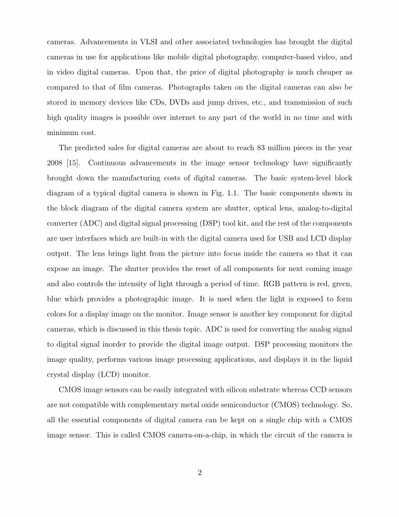
brought down the manufacturing costs of digital cameras. The basic system-level block
diagram of a typical digital camera is shown in Fig. 1.1. The basic components shown in
the block diagram of the digital camera system are shutter, optical lens, analog-to-digital
converter (ADC) and digital signal processing (DSP) tool kit, and the rest of the components
are user interfaces which are built-in with the digital camera used for USB and LCD display
output. The lens brings light from the picture into focus inside the camera so that it can
expose an image. The shutter provides the reset of all components for next coming image
and also controls the intensity of light through a period of time. RGB pattern is red, green,
blue which provides a photographic image. It is used when the light is exposed to form
colors for a display image on the monitor. Image sensor is another key component for digital
cameras, which is discussed in this thesis topic. ADC is used for converting the analog signal
to digital signal inorder to provide the digital image output. DSP processing monitors the
image quality, performs various image processing applications, and displays it in the liquid
crystal display (LCD) monitor.
CMOS image sensors can be easily integrated with silicon substrate whereas CCD sensors
are not compatible with complementary metal oxide semiconductor (CMOS) technology. So,
all the essential components of digital camera can be kept on a single chip with a CMOS
image sensor. This is called CMOS camera-on-a-chip, in which the circuit of the camera is
2

Analog SignalChain
ADC
Image sensor
DSP Image processing
UserInterface SDRAM Flash Memory USB
CCD Image Sensor
CMOS Image Sensor
RGB Pattern
Light
LCD ControlDisplay
Shutter Lens
Figure 1.1. Block diagram of a digital camera system.
made on a single chip. This reduces the cost, power consumption and also the size of the
camera [21], and hence can be suitable for portable electronic applications. CMOS mixed-
signal circuit technology allows the manufacturers to integrate all components in a chip so
that all functions like timing of ADC and exposure control are implemented on a single piece
of silicon. Fig. 1.1 also illustrates the difference between CCD and CMOS image sensor
present in digital camera system. Hence, CMOS image sensor on a digital camera system
combines sensor, ADC and image processing in one block. The unique features of digital
3

cameras allows their use in personal digital assistants (PDAs), webcams, cellular phones,
MP3 player, robotics and scientific applications. As CCD are older in technology, they have
excellent quality image with high mega pixel resolution cameras, this sensors are used in
many digital cameras like simple point and shoot types as the photo detecting sensor. CCDs
are still unrivaled for high sensitivity and long exposure time, low fill factor and low noise.
The advanced camera systems like single-lens-reflex (SLR) use CCD sensors. But, they are
not capable of clocking signals of the input which results in the complex system and high
fabrication cost. Use of APS in digital cameras improves the performance of cameras while
reducing its overall cost [66]. Typical example of such digital cameras include webcams,
cellular phone cams and PDAs, which has low resolution of less than 1 mega pixel.
Active pixel sensors are very much preferred from the system fabrication and integration
point of view than are CCD sensors, as the latter requires a separate fabrication process,
which results in high cost and also increases the size of the system. Recent model being nikon
D2X manufactured a 12.2 mega pixel with CMOS sensor type. The latest models of these
cameras are trying to introduce a new technology called junction field transistor lateral buried
charge accumulator and sensing transistor array (JFET LBCAST) which is also compatible
with CMOS technology [15]. Though research on CCD sensors is sill active, CMOS APS are
preferred over CCD sensor imaging as it enables fast processing of data and also mixing of
images. The technology developments of APS images are increasing by the day. The major
disadvantage of CCD sensors is that they consume large amounts of power for processing
larger photographs of high resolution, whereas APS combine with silicon substrate which are
compatible with CMOS technology and can be fabricated with other circuits. This occupies
less area and also reduces overall cost, as compared to conventional CCD sensors. CMOS
sensors help us in building a camera system on a chip [20]. APS use digital memory style
for reading data using row and column amplifiers which I will discuss in the later chapters.
This reading of data overcomes the problems of reading the data in the CCD image sensors.
APS draw more advantages as CMOS technology scales the transistor size, which results in
4

Table 1.1. Comparative advantages of CMOS APS sensor and CCD sensor.
Advantage Active Pixel Charged Couple
Parameters Sensor (APS) Device (CCD) Sensor
Image Quality Good
Technology Developing Matured
Pixel Size Small Larger
Processing Fast
Image Output Digital Film Based
Power Consumption Less More
the reduction of pixel size and hence they consume less power. The scaling of the CMOS
transistor technology reduced the sensor size and made the compatibility of APS design with
the silicon substrate on a digital camera system to form on one single chip, this result is
what is seen as mobile phone cameras with high resolutions. Recently, toshiba announced
that it was introducing a 3.2-megapixel and 2.0-megapixel CMOS image sensor lineup for
the integration with the mobile handsets [69]. The comparative advantages of CMOS APS
sensor over CCD sensor is summarized in the Table 1.1.
1.2. CMOS Image Sensors
Fig. 1.2 summarizes the various types of image sensors. Image sensors are primarily of
two types CCD and CMOS. The complexity of the circuit goes high when CCD sensor is used
along with CMOS circuits, whereas CMOS image sensors could be easily used along with
other CMOS circuits. CMOS image sensors are mainly of two types: Passive Pixel Sensors
(PPS) and active pixel sensors (APS). APS are the novel image sensors which have huge
potential because of the compact size and low power consumption. CMOS APS consists of
an array of pixels. Each pixel has a photodetector and three transistors - a reset transistor,
source follower or readout transistor and row select transistor. They have in-built amplifiers
for the amplification of the output signal.
5

Image Sensors
Charge Couple Device (CCD) Sensor CMOS Sensors
Passive Pixel Sensor (PPS)
Photodiode APSPhotogate APS
Snapshot APSPinned photodiode APS
Digital Pixel Sensor (DPS)Active Pixel Sensor (APS)
Figure 1.2. Hierarchical view of the image sensors.
The photosensing element used for APS can be a photodiode or photogate. The pho-
todetector accumulates the charge when light intensive rays fall on them. The capacitance
in the photodetector converts the charge into an electric voltage. This voltage conversion
can be reset by the reset transistor. When the reset transistor is turned ON, the photodiode
will be connected to the VDD clearing all the charge on the photodetector. The source fol-
lower transistor or read out transistor acts as buffer amplifier. It transmits the accumulated
charge of photodetector to the row select transistor. The source follower transistor works as
an active-current source load carrier. The voltage output is read on each column at the row
select transistor during capturing process. This design of APS is usually found in most of
the cameras.
1.3. Thesis Outline
In this thesis, I discuss the state-of-the-art technology of APS, different types of APS
and their performance, interms of noise and quantum efficiency. The developments and
applications of APS are also studied. I have reviewed some photodetector models for the
APS, such as photodiode and photogate and discussed the simulation results of photodiode
APS with AMI 0.6µm technology file. The attributes which lack in CCD image sensors and
6

are available in APS such as high sensitivity, high signal fidelity and huge array formats are
discussed.
The main objective of this thesis is to provide researchers with the state-of-the art infor-
mation about active pixel sensors. This thesis serves as a guide line for the research work
on the APS. Chapter 2 reviews related work, such as a basic review of photodetector mod-
els and image sensors such as charge couple devices and CMOS Image Sensors. In chapter
3, I introduce various types of APS and the basic architecture of APS array. I have also
emphasized on their respective quantum efficiencies and noise. Chapter 4 discusses the ex-
perimental setup and simulation results of photodiode based APS design. Chapter 5 reviews
the current state of CMOS APS by reviewing different research papers. It also presents the
developments and applications in the APS. Chapter 6 summarizes and concludes the work
done for this thesis.
7

CHAPTER 2
REVIEW OF PHOTODIODES AND IMAGE SENSORS
Photodetectors perform one of the main functions in all image sensors, that is, detection
of light and is therefore, an important component of the image sensors. Before the study of
image sensors in this chapter, we review the basic types of photodetectors. Silicon substrate
is used in most of the image sensors. There are two types of photodetectors, which basically
use silicon as a substrate: Charge coupled devices (CCD) and photodiodes. A photodiode
is one of the key components for sensing light and is usually used in active pixel sensors
(APS) to suit its working. The CCD sensors, which are one of the basic technologies used
for image sensing, have to be understood before discussing about the complimentary metal
oxide semiconductor (CMOS) image sensors.
2.1. Photodetectors
Photodetectors are devices that can absorb light and then convert them to electric sig-
nals, thus, eventually working as transducers. This implies that photodetectors are capable
of detecting optical signals of different wave lengths using semiconductor materials. Pho-
todetectors are used widely for light sensing in image sensors, security sensing, scientific and
industrial applications. The detection of light signals ranges with respect to wavelengths
of the optical range spectrum. However, I am concerned only about the visible range of
the spectrum, as digital cameras operate in the visible range of wavelength from 400nm to
700nm.
2.2. Basic Applications
Photodetectors operate based on the principle of light induced electron-hole generation.
When the light or the optical signal enters the material, the energy will be in the form of
photon energy (hv). In this process, the photons destroy the covalent bond, liberating an
8
electron. In other words, these photons excite carriers across the conduction band, reducing
the resistance of the material [16]. The energy of the photons being greater than the energy
band gap of silicon-1.123eV , they get absorbed by the silicon resulting in the excitement of
the electrons from the valence band to the conduction band, creating an electron-hole pair
(EHP) [24]. The energy bands for visible light wave lengths are indicated in Table 2.1. The
longest wave length of the visible light spectrum also provides sufficient energy in order to
excite electrons from the valence band to the conduction band in silicon. The generated
electron and hole pairs in depletion regions will then be swept by the junction field. The
current measured across this field is termed as the photocurrent. The rate at which the
electron hole pairs are generated per incident photon is given by a factor called quantum
efficiency. Quantum efficiency is given by the expression η [24]:
(1) η =I/e
P/hv,
where, P represents the power of illumination of photodiode, the produced current is given
by I, e is the charge, h is planck’s constant and is equal to 6.626 ×10⁻³⁴ J.s or 4.136 ×10⁻¹⁵
eV, and v is angular velocity. As the energy gap is less at large wavelengths, the quantum
efficiency becomes less. At small wavelengths, the photon is absorbed before reaching the de-
pletion layer, producing an electron pair that can recombine. At its peak, quantum efficiency
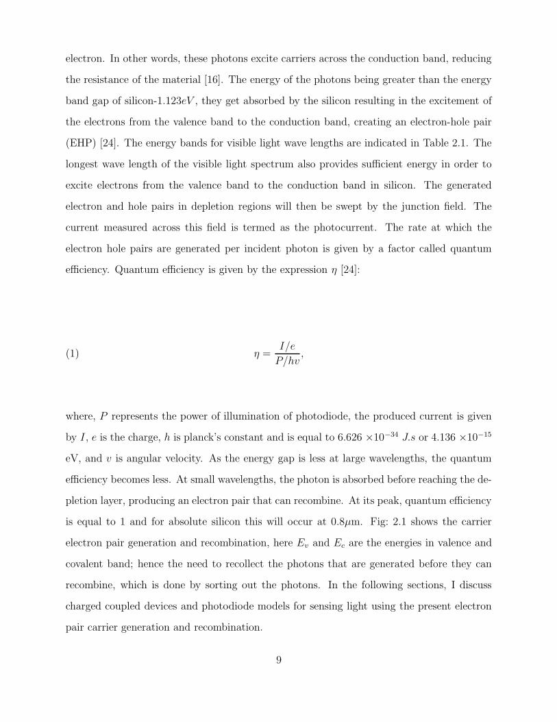
is equal to 1 and for absolute silicon this will occur at 0.8µm. Fig: 2.1 shows the carrier
electron pair generation and recombination, here Ev and Ec are the energies in valence and
covalent band; hence the need to recollect the photons that are generated before they can
recombine, which is done by sorting out the photons. In the following sections, I discuss
charged coupled devices and photodiode models for sensing light using the present electron
pair carrier generation and recombination.
9

Table 2.1. Energy bands for visible lights.
Visible Lights Wavelengths Energy bands
Green 510nm 2.43eV
Red 650nm 2.43eV
Green 475nm 2.610eV
E ph > E g
E
E
c
v
E
Ionization due tocharged high−energy particles
Q
generation of carrier recombination ofcarrier
Figure 2.1. Electronpair carrier generation and recombination [6].
2.3. Charge Coupled Devices
Charge coupled devices were invented by Boyle and Smith in 1969 at Bell laboratories
[54]. Using the novel technology of metal-insulator semiconductor (MIS) device, a new
storable device was invented for computers, called, charged couple devices [47] [62]. The
first image sensor was fabricated in low resolution television of 64 × 106 arrays which is
like using 13000 CCDs [57]. Later evolved many applications of CCDS and in 1974, the
first astronomical CCD image was constructed with 100 × 100 pixels CCD array of 8-inch
telescope by Fairchild Electronics [14] [49]. Later, the concept of traditional image camera
replacement was considered.
10

The first CCD was constructed on metal oxide semiconductor (MOS) capacitor.The phys-
ical structure of a metal oxide semiconductor is shown Fig 2.2. Initially Cr-Au metal was
used as metal layer and oxide as silicon dioxide, thus constructing a metal oxide semiconduc-
tor capacitor [22]. The polysilicon is also used in the CCDs image arrays, where the arrays
of MOS transistors are closely packed. Single MOS transistor shows a pixel of a CCD image
array. The depth of the well depends on the function of gate voltage applied, which is set
at the staring point to keep charge below the third electrode. The potential on the that
line of electrode is dropped with the increase of the potential in the neighboring cells thus
creating one large well that can store all the charge. At the end of the cycle the second well
is decreased while the first one is increased transferring the charge over by one pixel. This
cycle pattern is repeated till the charge on each pixel is sequentially read out at end of the
row. The above scan lines drive the active charge from the periphery of the chip, with each
pixel transferring the charge to its neighbor. The top layer along with metal in the metal
oxide semiconductor forms the gate [58, 59]. In the previous sections, I have mentioned
that shorter wavelengths will lead to poor detection by the photodetectors. This is true for
charge coupled devices, as most of the power gets absorbed by the gate. This is because
of the penetration depths with which the light signal hits the gate. Table 2.2 shows the
penetration depths of different wavelengths [46]. From the penetration depths table, we can
observe that the CCDs observe 90% of the photons hitting the metal oxide semiconductor.
2.3.1. Working of CCD Devices
The concept of charge coupled devices revolves around the operation of metal oxide
semiconductor capacitor. A CCD pixel accumulates the photons-induced charge on the
potential well; this potential well is formed when the positive charge or the light intensity
falls on the gate of the metal oxide semiconductor. This causes carriers to form a potential
well so that it can store the charge that was formed when electron pairs where created due to
photons induced on the gate of the metal oxide semiconductor. This potential well collects
the electrons before they recombine and the holes are separated by the substrate.
11

metal
semiconductor
oxide
t 1
2
4
t 0
t
t 3
t
Figure 2.2. Working of charged couple devices [24].
The image array of CCDs is an array of MOS transistors closely packed. Single MOS
transistor shows a pixel of a CCD image array. The depth of the well depends on function
of gate voltage applied, which is set at the starting point to keep charge below the third
electrode. The potential on that line of electrode is dropped with the increase of the potential
in the neighboring cells. Thus, creating one large well that can store all the charge. At the
end of the cycle, the second well is decreased while the first one is increased, transferring
the charge over by one pixel. This cycle pattern is repeated till the charge on each pixel is
sequentially read out at the end of the row. The above scan lines drive the active charge
from the periphery of the chip, with each pixel transferring the charge to its neighbor.
12

Table 2.2. The penetration depths of different wavelengths.
Wavelengths (Nanometers) Penetration Depths (Micrometer)
400 0.19
450 1.0
500 2.3
550 3.3
600 5.0
650 7.6
700 8.5
750 16
800 16
850 46
900 62
950 150
1000 470
1050 1500
1100 7600
2.3.2. Development of CCDs
The development of CCD fabrication started 30 years ago. Present day CCDs provide low
noise and also high speed along with high resolution and high fill factor [29]. Some special
CCDs like fujifilm’s superCCD, superCCD HR, and superCCD SR have been developed [63].
The latest development in CCDs includes increase in sensitivity, dynamic range, signal to
noise ratio, and also reduced pixel pitch. The CCDs are widely used in point and shoot-type
digital camera. Novel CCDs are cost effective and at the same time have higher yield. CMOS
active pixel sensors are more compatible with digital cameras as they are integrable onto a
single chip which is not possible in the case of the CCDs. Also, CCDs do not contribute
13

much towards the lower end cameras like PDAs, webcams, and cell phone cameras due to
power inefficiency and as a result are driving researchers to obtain low-power sensors [11].
2.4. Photodiode
A photodiode is the next type for photodetectors. A photodiode acts as the main model
for the photodiode based active pixel sensor. Photodiodes are fabricated from semiconductor
materials, silicon in particular. Silicon photodiodes are preferred to materials like gallium ar-
senide (GsAs), indium antimonide (InSb) or indium arsenide (InAs). Silicon absorbs 260nm
to 1100nm. Silicon photodiodes are generally formed by joining the p-type and n-type sili-
con. The junction forms a depletion region in which an electron pair carrier is formed. This
diffusion results in the formation of holes. The current formed due to formation of hole and
electrons in the depletion layer is called diffusion current. Fig 2.3 shows the formation of dif-
fusion current. There will be a net charge formed due to the depletion layer of un-neutralized
silicon ions. This net charge, in turn, creates an electric field which causes drift current.
+
+
+
+
−−
−−
E
E
Ec
f
v
X X
P
p n
+hole diffusion
N
+ +
+
−
−
++
−−
−
e−diffusiondepletion region
−
Figure 2.3. Depletion layer of photodiode[10].
14

2.4.1. Operation of Photodiode
When photon light is absorbed, the photodiode excites an electron and produces a single
pair of charge carriers like an electron and a hole. The holes are the absence of the electron
in the semiconductor lattice. Current passes through the semiconductor when the charge
carriers are separated and travel in opposite directions. The photon-induced charge carriers
are collected as current or voltage at the electrodes before they recombine. This is done
using the pn or p-n junction structure, hence the name p-i-n photodiodes. When a voltage
is applied to the p-n junction, holes will be attracted to the p-side of the p-n junction,
and then the reverse biased condition arises. The increase in the depletion layer will allow
the photodiodes to collect more photons or would result in the increase in the storage of the
electrons. The formation of electron-hole pair generation can be seen in Fig 2.4. The increase
of the depletion layer may result in the increase of the transit time and the response of the
photodiode model may be reduced. Desirable performance characteristics are essential with
respect to response speed, quantum efficiency, and dark noise of a photodiode. Optimization
of its size should be considered due to its importance in APS.
−−
−−
−
−
−+
++
+
+
++p−sub n−sub
depletion regionp−region n−region
recombineswept apart
photons
recombine
Figure 2.4. Eletron-hole pair generation in photodiode.
2.4.2. Photodiode Model
Accurate models for photodiodes in CMOS image sensors, with high frequency and opti-
mal size are discussed in [64]. The photodiode can be modeled with a diode, current source,
15

capacitor and two resistors. The model discussed in this thesis is proposed by Swe and Yeo
[64]. The photodiode model is shown in Fig 2.5. The terms in the photodiode model Rs is
called as series resistance which arises from the contacts and the resistance of the undepleted
silicon and Rj is called as the junction resistance which varies along with the current of the
photodiode.
Diode C R
R
Ip j j
s
Figure 2.5. Photodiode Model
Using the symbols defined in table 2.3, the photocurrent is calculated by expression [65]:
(2) Ip =qηPopt
hv=
qηPopt
hvλ
.
The depletion capacitance or the junction capacitance is calculated using the following ex-
pression [56],
(3) Cjdep =cj.AD
(
1 + VDB
pb
)mj+
cjsw.PD(
1 + VDB
pbsw
)mjsw.
The typical value of the capacitance taken for active pixel sensor simulation is 1pf , for AMI
0.6µm n-well CMOS transistors. The design and the simulation results of active pixel sensor
are discussed in the Chapter 4. The series resistor and also the junction capacitance can
also be calculated [53, 65].
2.5. CMOS Image Sensors
Multi-media applications such as digital camera systems, automobiles, and computer
based videos have made image sensors gain high research volume, insisting on researchers to
16

Table 2.3. Parameters used in description of photodiode model.
η quantum efficiency of the photodiode
q Charge of Electron=1.602 ×10⁻³⁴ in Js
v Frequency
Popt Optical Power
c Speed of Light=30 ×108 m/s
λ Wavelength
h Planck’s constant in Joule-Sec
cj Zero-bias depletion capacitance
cjsw Sidewall zero-bias depletion capacitance
AD Area of diode
PD Periphery of diode
VDB Voltage across the diode
pb built-in potential
mj grading coefficient
pbsw built- in potential of the sidewall
mjsw grading coefficient of the sidewall
build a CMOS based image Sensor which can integrate with silicon circuits. CMOS image
sensors consume less power and are faster. The CMOS image sensors are of mainly two
categories: Passive pixel sensors (PPS) and active pixel sensor (APS). Active pixel sensors
are more widely used than passive pixel sensors, as the latter have numerous disadvantages
over the former. The main area of research now is based on the CMOS APS than the CCD
image sensors. The basic block diagram of a CMOS image sensor is shown in the Fig.2.6
[77]. The block diagram of CMOS image sensor has its key component as a pixel array. Pixel
array can be made of any CMOS image sensor according to the size of the array such 1,024
× 1,024 photodiode based active pixel sensor (APS) array or photogate APS. Row decoder
reads the rows of the pixel array one row at a time using on chip timing control. The noise
17

X−Addressing(column decoder)
Chosen pixel
Pixel Array
General Output
column amplifier
(row decoder)
Y−A
ddressing
analog mux
Figure 2.6. Block diagram of CMOS image sensor [77].
in the pixel is reset by the sensing node of photodiode while row decoder access one row at a
time. Column amplifiers provide signal strength to the pixel output and then read the pixel
output to the rest of the system using the column decoder. The analog multiplexer, sample
and hold circuit and correlated double sampling circuit (CDS) are provided on one block for
temporary memory storage and also to remove the unwanted signal.
2.5.1. Passive Pixel Sensors
The passive pixel sensors (PPS) were introduced by Weckler in 1967 [72]. The working
of a PPS is similar to that of an single-transistor DRAM cell [12]. Though PPS are not as
efficient as the active pixel sensors and CCDs, they have one important advantage - high
fill factor in lower area, which leads to high quantum efficiency. The schematic view of a
passive pixel sensor is shown in the Fig: 2.7. It can be observed that passive pixel sensor
contains a photodiode and a transistor and this transistor is also called as thin film transistor
18

Vref
Reset
Col 1RS
Pixel
Pixel
Pixel
+
−Vout
Figure 2.7. Schematic of passive pixel sensor [23].
(TFT). The transistor TFT does the reset and row selection of the pixel information. There
is charge integration amplifier (CID) for each column in the array; this is used to keep the
voltage constant on each bus of the array in the passive pixel sensor.
Passive pixel sensors have three modes of operation: Reset mode, integration mode
and readout mode. In the reset mode, voltage is taken as a reference, in order to reset the
photodiode for carrying next pixel information. This is done mainly before the integration of
time. During this period, the photodiode discharges its current at a rate which is proportional
to the amount of the incident light illumination falling on the photodiode. In the integration
mode, the TFT is switched ON and the signal accumulates the charge on the photodiode
according to the radiation of the pixel. In the readout mode, the accumulated signal charge
is read out as final voltage. The PPS has a major disadvantage due to its large capacitive
loads, as the larger bus is directly connected to each pixel during its readout. Passive pixel
19

sensors cannot be used for larger array sizes or faster pixel readout rates; it causes fixed
pattern noise, FPN noises are due to the different individual amplifiers. Researchers are
still working on the implementation of PPS arrays with FPN reduction techniques [31]. The
passive pixel sensors are also used in medical imaging [34]. Passive pixel sensors are more
useful for small pixel size and less fabrication cost.
2.5.2. Active Pixel Sensors
Active pixel sensors came into existence when Fossum introduced them in 1992 [21] in
NASA‘s Jet laboratory. Active pixel sensors overcome the problems that are exhibited by
PPS. Active pixel sensors have one or more active transistors used to buffer and amplify
the signal and to read out the output as voltage. APS are advantageous in terms of low
power consumption and low cost over the CCDs and have attracted researchers to work on
its many applications, useful in various types of digital systems like webcams, automobiles,
digital cameras, toys, computer based video games, etc. Power optimization, reduction of
dark current, reducing fault tolerance, noise reductions, reducing pixel size [8, 26, 42, 17, 30]
are some of the attributes that enticed the researchers in the present portable appliance
scenario. Active pixel sensor also has some other advantages over CCDs such as
(1) High sensitivity,
(2) Fill factor which is typically about 50-70 percent,
(3) Computability with CMOS technology due to the capability to build more pixel
arrays resulting in more system-on-a-chip (SoC) integration,
(4) Lower cost,
(5) High readout speed, and
(6) Less power consumption.
The basic architecture of active pixel sensor array is shown in Fig: 2.8. The core part of
the APS architecture is the APS array, which is connected to the row decoder for decoding
the signals of a pixel in a row by row fashion. The decoded signal is read out to the parallel
column first, which converts the analog signals to the digital signals and then later is read out
20

X−Addressing(column decoder)
General Output
(row decoder)
Y−A
ddressing
analog mux
Pixel Array
column amplifier
photoDectector
Amp
Figure 2.8. Architecture of active pixel sensor array [77].
to the rest of the available system on the architecture. Active pixel sensors are of three types:
Photodiode APS, photogate APS and pinned photodiode APS. Photodiode active pixels and
photogate APS are used more often. Advantages of photodiode APS over the photogate APS
and the different types of APS will be discussed in chapter 3. The architecture discussed
here is used in many systems like CMOS image sensor with watermarking capabilities [50].
The basic comparison of APS and PPS is shown in the Table 2.4.
2.5.3. Differences of APS and CCD Sensors
The basic differences between the CCDs and APS systems will be discussed in this section.
Both active pixel sensors and charged coupled devices sensor are used in digital cameras.
These sensors have their own advantages and disadvantages according to their perspective
of usage in the systems. In general, the CCD sensors have a much more matured technology
than APS sensors. As of now, APS is growing at a very fast pace in terms of technological
21

Table 2.4. Basic difference of APS and PPS sensors.
Parameter APS Sensor PPS Sensor
Size Larger Smaller
Fill Factor Good
Quantum Efficiency Good
Fabrication Cost High Low
Larger Pixel Array Good
Capacitance Load Low High
Readout Modes Fast Slow
improvements and may eventually replace the CCDs as the sensor of choice. Compatibility
to CMOS technology resulting in camera on chip integration, less power consumption, faster
readout circuitry when compared to CCDs are some of the advantages of APS. Both APS
and CCD sensors are based on the silicon technology. Though the characteristics of silicon
for the visible and infrared wavelengths are similar, the CCDs and APSs circuit operation is
totally different in these regions. Charge coupled devices image sensors need to have a perfect
charge transfer for reading the value from pixel to pixel in an array and hence are hard to
integrate with other circuits on the board of a camera chip. High frequency operation also
becomes difficult in CCDs [21]. Larger arrays consuming large areas make the CCD system
complex affecting the cost criteria. The CCDs are said to achieve the same performance of
APS, but the cost of fabrication for the CCD sensor will be thrice as that of APS.
The disadvantages of the CCDs are overcome by the APS like charge transfer efficiency
and cost of fabrication. The speed of the APS sensor in reading the information to the rest
of circuit is also fast. Though the integration of CCDs with other circuits is not impractical,
upon that the signal processing clock for CCDs sensor becomes tough. This clock timing
is very important for processing the analog signals through the analog-to-digital converter
(ADC). In active pixel sensors, ADC can be built on the same chip which leads to the camera-
on-a-chip with digital system, making interfacing possible with external systems. Active
22

pixel sensors are computable with mixed signals as they develop similar characteristics as
of analog CMOS technology. With this advantage, the active pixel sensor has compact size,
less weight and also less power consumption and low cost.
Charge coupled device sensors provide good image quality for higher wavelengths ranging
from X-rays to infrared region unlike the APS which cannot compete with CCDs due to noise
made by active transistors called as the fixed pattern noise (FPN). This FPN can be reduced
by using correlated double sampling on the signal after it is processed from the APS sensors.
Active pixel sensors have poor resolution when compared to the CCDs due to poor fill factor
which is the ratio between the photo sensing area in each pixel to the total area. Table
2.5 gives the basic difference between CCDs and APSs, with the facts evaluated by Dave
Litwiller [39].
Fine tuned optical CMOS process in active pixel sensor architecture helps to achieve the
image quality of CCDs [67]. A process with the CCD and APS combined would yield very
good results, but this area of research is not yet predominant due to the factors related to
testing, technology and fabrication related costs [41]. Both CCDs and APSs dominate the
sensors industry in their own way. CCDs are used in digital cameras such has Single-Lens-
Reflex (SLR) for good quality images and APSs are used in webcams, toys due to their low
power consumption and compact size. Future CMOS image sensor technology growth would
yield good image quality with compact sized, low power sensors.
2.6. Summary
In this chapter, I have discussed the basic types of silicon photodetectors present in the
digital camera in the consumer applications- Photodiode, Charge Couple devices sensors.
Also presented here are the basic types of CMOS image sensors- Passive pixel sensor (PPS)
and active pixel sensor (APS) and their operations, with the basic differences between active
pixel sensor (APS) and charged couple device (CCD) sensors.
23

Table 2.5. Basic difference of CCD and APS sensors.
Parameter APS sensor CCD sensor
Cost Cheap
Fill Factor Good
Quantum Efficiency Good
Reliability Good
Biasing Clocking Significantly good
Anti-Blooming Inherent
Image Access Good for low contrast images
Speed Good
Responsivity Good
Shuttering Good
Output Linear Non linear
Integration Functional
Market Advantages Greater levels of integration Known capabilities
(USB, Firewire) for CCD
Noise Low temporal noise Low spatial noise
Application Low end cameras High end Cameras
(webcams, mobile-phone cameras) (SLR cameras, X-rays)
24

CHAPTER 3
TYPES OF CMOS ACTIVE PIXEL SENSOR
According to Moore’s law the total number of devices in a VLSI chip will be doubled
in CMOS technology for every 26 months [18]. The exponential development of the CMOS
technology is also making good developments in APS and as a result, the circuit on chip is
much miniaturized and is also very cost effective. Researchers currently propose different
types of APS depending upon high quality of image and good frame rates [3, 27, 33, 36,
40, 45, 48, 51, 60, 78, 79]. In the next chapter we discuss about the different type of active
pixel sensor and their differences in aspects like quantum efficiency, fill factor and noises.
Photodiode APS and photogate APS are the most commonly used types which are discussed
in detail in the following sections including other forms of pixels of APS.
3.1. Photodiode Active Pixel Sensor
Photodiode APS was introduced by Noble in 1968 [52]. F. Andoh et.al, tested a 2, 50,000
pixel image with FET amplification for high speed television cameras in 1980s [2]. Later,
a novel model of APS with random access memory and electronic shuttering was proposed
by the Yadid-Pecht in the beginning of 1990s [75]. Photodiode APS has high compatibility
with CMOS technology resulting in its higher utilization over CCD sensors. Eric Fossum
developed the photodiode APS in NASA laboratory in 1993.
The schematic view of a basic photodiode APS is shown in Fig. 3.1. It consists of a
photodiode used for sensing light, three NMOS transistors called the reset transistors, a
source follower transistor called as a buffer transistor and a row select transistors.
The light rays are converted into charge and then the charge to voltage conversion is
done at the sensing node capacitor of the photodiode when the reset transistor if OFF. The
photodiode resets to the reference voltage when the reset transistor is ON. This reference
25

Transistor(VDD on Gate) Reset Transistor Transistor
row_select
Colu
mn
Bus
Photodiode
Sourcefollower
Light
Vdd Vdd
Figure 3.1. Basic photodiode active pixel sensor [77].
voltage is set in order to remove the dark current at the CDS circuit, shown in architecture of
APS. The voltage sensed by the photodiode is transmitted to the source follower transistor
which behaves like a buffer amplifier, once the charge to voltage conversion is done. In
order to keep the fill factor high and to reduce the pixel to pixel variation, the source
follower transistor is used at each and every pixel. The data is read out when the row select
transistor is enabled.
The four transistor photodiode APS provides a high dynamic range [9], which is one of
the many recently proposed ideas on low-noise and high-fault tolerance photodiode APS.
Different techniques to reduce dark current, which is one of the main problems that APS
suffer from, are proposed. Pseudo active pixel sensor (PAPS), a new pixel which allows
larger array size in CMOS still image applications has been proposed for low dark currents
[61].
3.2. Photogate Active Pixel Sensor
The photogate APS was introduced at the jet propulsion laboratory (JPL) in 1993 [43].
This pixel is used for high performance scientific imaging and low light applications. The
26

basic operation of photogate APS arises from CCD technology. The photogate APS has the
benefits of CCD sensors.
Transistor(VDD on Gate) Reset Transistor Transistor
row_select
Colu
mn
Bus
Sourcefollower
TXPG
Vdd Vdd
Figure 3.2. Schematic view of photogate active pixel sensor [77].
The basic schematic of the photogate APS is shown in the Fig. 3.2. The photon-generated
charge is accumulated underneath the photogate in the potential well. In the integration
mode, the photogate is turned ON, during this the potential well is created for charge storage.
Then the output of the signal is read depending on the pulse signal on the photogate to the
source follower transistor. Then a reference voltage is taken generated by the photogate
during the reset mode. The difference between the voltage signal during the integration
mode and the reset mode gives the output of the sensor. The signal is read out to the sample
and hole of correlated double sampling (CDS) as shown in the architecture of the APS array.
CDS circuit removes the reset noise and fixed pattern noise due to the threshold voltage
variations. The reduction of this noise level in the photogate APS increases the dynamic
range and the signal-to-noise ratio (SNR). In the photogate APS circuit the transfer gate is
built-in with the help of the poly layer in-between the photogate and readout transistor are
27

ideally overlapped using double poly process. Transfer gate acts like a smaller CCD circuit;
it controls the photon generated charge flow but not the light detection.
But the shot noise produced due to the photogate cannot be removed. Hence the photo-
gate APS uses five transistor and has a pixel pitch equal to 20 times of the minimum size of
the technology. Motion detection was also implemented in the photogate APS by changing
the timing of the sensor. So that the last frame is also stored on the floating diffusion before
the next frame is integrated under the photogate. Output will be the difference of the con-
secutive frames. A 256 × 256 element CMOS APS is reported with motion detection was
reported by the JPL [13].
3.3. Difference of Photogate APS and Photodiode APS
There are many differences between the photogate and photodiode APS. It is observed
that the photodetector element for the photogate and photodiode APSs are different. The
photogate APS uses photogate as the photodetector. Photogate has ploysilicon on the top
of the layer which reduces the response of the lower wavelengths like blue light. Hui Tian, et
al., reported that there will be 5% less efficiency for wave lengths under 450nm [68]. In the
schematic of photodiode APS Fig 3.1, we can observe that the photodiode node is shared
by the gate of the readout transistor. Due to this the sensitivity of photodiode APS goes
down [44]. But comparatively, photodiode APS has more sensitivity than the photogate
APS at lower wave lengths. The photogate APS has five transistors which may result in
decreased fill factor compared to the photodiode APS. This makes the system complex in
photogate APS compared to photodiode APS. Photogate APS has an extra control signal in
its architecture which causes an increase in power consumption compared to the photodiode
APS. The gain of the photogate APS will be more than that of photodiode APS.
For photogate APS noises such as shot noise and the thermal noise are major draw backs.
These noises are caused due to the various factors like pixel-pixel array variation, threshold
voltage variation and power supply fluctuations. Some of these noises can be removed by
the correlated double sampling (CDS) circuit which is present in the APS architecture. But
28

the implementation of CDS circuit in photogate APS is more complex than in photodiode
APS. But another techniques called double sampling is implemented in photodiode APS.
But we cannot suppress the noise in the APS for photodiode based APS model than that
of photogate. Some of basic differences between photgate and photodiode APS are shown
in the table 3.1. The photogate APS and photodiode APS have their own advantages with
respect to photodetectors they are using. The better APS will be based on the application
used.
Table 3.1. Difference of photogate and photodiode APS.
Parameter Photodiode APS Photogate APS
Fill factor High Low
Power consumption Low Little high
Control signals Simple Complicated
Responsivity Better for Poor for
low wavelengths low wavelengths
Sensitivity High Low
Multiple integration Not possible Possible
Sampling technique Correlated Double sampling
double sampling (CDS) (DS)
Total Capacitance at Output Cphotodiode + Cgate Cgate
Quantum Efficiency More Less
3.4. Pinned Photodiode APS
Reduction in noise occurs when the reset is completely achieved in photodiodes which
results in all the mobile electrons to be removed during the reset stage of the photodiode.
Pinned photodiode APS has the functionality of resetting the photodiode completely. Pinned
photodiode are used in CCDs previously, but later it was proposed to be used in the APS for
complete reset. The pinned photodiode APS has a pinned diode of (P +n−p), in this pinned
29

diode the photon collection is moved from surface in order to reduce the surface noise like
dark current [28]. The operation of photon collection in the pinned photodiode is similar
to that of the photogate APS. The photon generated charge is integrated below the pinned
diode and then the charge output is transferred to the readout transistor or source follower
transistor. In pinned photodiode the sense node and the integration node are separated
inorder to reduce the noise. The potential well for the pinned photodiode is formed by a
buried intrinsic layer or an n-type layer. The basic pinned diode APS is shown in the Fig. 3.3.
Transistor
Reset Transistor Transistorrow_select
Colu
mn
Bus
Sourcefollower
n+p+ n+
TX
P−substrate
Vdd
V Vdd dd
Figure 3.3. Schematic view of pinned photodiode active pixel sensor[77].
Pinned photodiode has five control lines and four transistors. This pixel has high fill
factor than that of photogate APS and less than that of the photodiode APS. This has low
quantum efficiency. Pinned photodiode APS are good for reducing the dark current. They
increase the blue response by collecting the blue electrons generated near the silicon-silicon-
diode interface with the pinned photodiode. This increases the cost and the yields for the
removal of dark currents [25, 37].
30

3.5. Snapshot Pixel Sensor
Snapshot active pixel sensor was designed by Yadid Pencht in 1991 for low noise and
high speed imaging. In most of the CMOS image sensor rolling readout method is used. In
this method a shutter is introduced in between the sensing node of the photodiode and the
source follower transistor as shown in Fig. 3.4.
Reset Transistor
Vdd
Photodiode
SourcefollowerTransistor
data
Transistorrow_select
Shutter
Vdd
Figure 3.4. Schematic view of snapshot photodiode active pixel sensor[77].
The cell can be shuttered to prevent the charge accumulation. In this approach, the start
and end of the photon or light collection is delayed in the pervious rows. This allows us to
take the relative motion of the images. So this technique is an ideal solution for imaging
of the moving objects at a faster pace. This method is called as electronic global shutter
method [76]. Each pixel has a memory element in order to provide the capabilities similar
to a mechanical shutter. It allows to read the entire pixel array before the integration and it
will stop exposure during the reading of the image data. In the global shutter technique, the
shutter exposes all the pixels unlike the rolling shutter technique. In snapshot photodiode
31

APS architecture, a sample-and-hold circuit is provided with analog storage containing the
parasitic capacitances of the amplifier input. The amplification of the output or data is
provided within the pixel by the source follower transistor. During the integration time of
the snapshot APS, the signal charge is stored in the sample-and hold circuit. However, one
problem in snapshot photodiode APS is that during the light exposure of snapshot APS,
the leakages of the shutter and small storage of the capacitance may lead to the loss of the
signal. The snapshot pixel has small pixel area as the shutter is provided by the NMOS
transistor. The NMOS shutter provides low efficiency compared to PMOS efficiency. The
shutter efficiency can be increased by replacing the NMOS shutter with PMOS. But, PMOS
has low fill factor and this may result in the decrease of conversion gain. Snapshot photodiode
APS is provided with anti blooming.
3.6. Digital Pixel Sensor
In digital pixel sensor (DPS), each pixel consists of a photodetector, analog-to-digital
converter (ADC), and a digital memory for temporary storage of data before digital output
signal is read out. The main advantage of this pixel is that analog to digital conversion of
the data is done within the pixel and the final output is read in terms of digital bit line.
This pixel array can be accessed randomly from digital memory provided. Sensing light can
be performed by photodiode or photogate that may be used depending on the applications
of usage. DPS has several advantages over analog image sensors such as passive pixel sensor
and APS. DPS provides better scaling with CMOS technology, also reduces FPN noises and
readout noises. More importantly DPS provide Snap-shot technique for images. It has fast
read out modes. Fig. 3.5 show the basic schematic of digital pixel sensor. In recent years
many work on digital pixel sensor are reported [35, 70].
The main disadvantage with DPS is that the number of transistors will increase as that
of active pixel sensor (APS) which will result in the increase of pixel size or low fill factors.
The most recent reported digital pixel sensor was with 0.18µ CMOS technology which will
integrate both on single-slope parallel ADC and on 8-bit dynamic memory inside each pixel
32

Col 1
Pixel
Pixel
Pixel
MemoryADC
PN
SenseAmp
OutDigital
Figure 3.5. Schematic view of digital pixel sensor [23].
[35]. This pixel was the first one reported for achieving the continuous throughput of 10,000
frames per second. There is much research work going on the development of this pixel.
3.7. Modes of Pixel Operation
Active pixel sensor functions on two modes of operation: Linear integration mode and
logarithmic mode. High signal to noise ratio and large output signals are obtained in the
linear integration mode. Increased dynamic range of operation is obtained in the logarithmic
mode. The control input signal selects the mode of operation depending upon the APS
imaging application. The APS sensor array is operated by selecting one row at a time using
row select transistor as shown in the schematic of APS. The detected signals are transferred
to the sample-and-hold circuit, which are read row by row. In the architecture of APS, the
auto scan of the APS array is implemented by a counter which generates the signal to the
row and column.
33

3.7.1. Linear Integration Mode
In the linear integration mode, the APS is reset by the reset transistor; the reset transistor
is turned off for the integration of the charge on photodiode. The charge to voltage conversion
is done using the sensing node capacitance. The rate of the decay of this bias voltage is given
by Nobel [52]:
(4)dV
dt=
1.2λPη
c,
where P is the incident power and λ is the wavelength in µm, η is the efficiency and c is the
velocity of light. The charge on the photodiode is read out to the source follower transistor.
Then using the row select transistor the final output voltage is read to the correlated double
sampling. The output voltage is directly proportional to the light intensity that falls on the
photodiode. The photodiode APS of integration mode is shown in fig 3.1. The ideal response
of the voltage is independent of the diode area. The parasitic capacitance of photodiode may
affect the area.
3.7.2. Logarithmic Mode
Logarithmic mode of the photodiode APS is described in the Fig. 3.6 [55]. This circuit
enables the logarithmic encoding of the photocurrent, increasing the dynamic range of pho-
todiode APS. In this the pixel does not have any reset and operates continuously. The reset
transistor works in a weak inversion region. As there is no reset for the photodiode the
dark current is converted to the output voltage. The voltage on the photodiode (VPH) will
be approximately equals to the power supply (VDD). The output voltage will vary as the
following expression:
(5) VA =−kT
q× ln
(
Iph
I0
)
,
where, VA is the output voltage, I0 is a constant. The voltage on the photodiode decreases
logarithmically with linear increase in the illumination. But the main drawbacks of this
34

logarithmic mode are slow response at low light intensity and low swing in the output
voltage, leading to a low signal to noise ratio [7].
Transistor
Transistorrow_select
Photodiode
Sourcefollower
Data
Vdd Vdd
(VDD on Gate) Reset Transistor
Figure 3.6. Logarithmic mode of photodiode active pixel sensor.
Logarithmic mode of operation in APS has more dynamic range than compared with
the linear integration mode operation in APS. In the logarithmic mode of operation, I have
seen that the output voltage is temperature dependent, because of which it may have less
affect on the output voltage swing compared to the linear integration mode. Moreover,
the logarithmic mode needs a extra circuit for removing the noise compared to other APS
systems. The differences of the APS linear integration and logarithmic mode are shown in
the table 3.2.
3.8. Summary
In this chapter, I have reviewed the different types of APS and their working modes.
Among all the APS, photodiode APS model is used in most of the consumer applications.
I have presented the basic differences of photogate APS and photodiode APS and discussed
about the quantum efficiency and signal to noise ratios. There is wide research going on APS
and its different designs in-order to reduce dark currents, noises and to make the system read
fast and optimize the power. But photodiode APS serves as the basic model. Recently, a
35

Table 3.2. Difference of APS linear integration and logarithmic mode.
Parameter Logarithmic APS mode Linear APS mode
Fill factor High Low
Dynamic range High Low
Random access Possible Not Possible
Temperature dependence High Low
Output voltage swing Low Better
FPN Noise High Low
Circuitry Complex Less complex
Cost High Low
4-transistor photodiode APS has been reported [38]. Two novel modes of operation of APS,
logarithmic mode and integration mode have also been reviewed in this chapter.
36

CHAPTER 4
SIMULATION OF AN ACTIVE PIXEL SENSOR
In this chapter, I present the design and simulation results of photodiode APS and also
an optimization technique used for scaling the photodiode APS to present nano CMOS
technology. The current problems associated with photodiode APS optimization are also
discussed in this chapter.
4.1. Design of Photodiode Active Pixel Sensor
Design and simulation results for photodiode active pixel sensor are extracted using virtu-
oso schematic editor from cadence r©[32]. Though there are many other CMOS technologies
used for simulating photodiode APS, I have used AMI 0.6µm n-Ill CMOS technology. The
operating voltage supply for this technology is 5V which is used for the design of photodiode
APS. Photodiode APS consists of a photodiode and three NMOS transistors: Reset tran-
sistor, source follower transistor, and row select transistor. Photodiode, the sensing element
for the light intensity, converts light intensity into current with the help of its sensing node.
The charge resulted is converted to the voltage by the capacitance of the photodiode at the
sensing node. Design of the photodiode in the schematic shown in fig. 4.1 is modeled with a
current source (IPhoto) and capacitance of the diode (Cdiode). A biasing circuit is added to
the pixel which provides a constant current sink to the source follower transistor thus keeping
it in saturation region. The biasing circuit is modeled with capacitance (Cline) and biasing
current source (Ibias). Source follower transistor acts as a buffer amplifier to segregate the
charge of the sensing node. Source follower transistor is an active current source load carrier
which is located on each column of the APS array to avoid pixel to pixel variation. The
output of this transistor is read out to the correlated double sampling circuit by enabling
the row select transistor. The reset transistor resets the charge on the photodiode.
37

+−
+−
Reset Transistor
SourcefollowerTransistor
Data
Transistorrow_select
Vreset
IphotoCdiode
1pf
Vrow_select
Cline IBIAS10uA500fF
Vdd
Figure 4.1. Design schematic of photodiode active pixel sensor.
4.2. Simulation Results
Photodiode active pixel sensor operation is divided into three stages: Reset Stage, in-
tegration stage and the read out stage. Provided with the pulse voltage waveform on the
gate, the reset transistor is turned ON at the positive pulse of the wave form. The charge
on the photodiode is reset by turning ON the reset transistor. Reset voltage is read out as
a reference voltage to one of the sample-and-hold in the correlated double sampling(CDS)
as shown in the architecture of the APS. The CDS circuit subtracts the signal pixel value
from the reset value in order to avoid the fixed pattern noise caused due to the pixel-pixel
variation.
Integration stage follows the reset stage. When the reset transistor is turned OFF,
the light intensity hits on the surface of the photodiode, generating photon charge. The
capacitance of the photodiode discharges through a constant time at rate proportional to
the light intensity. The high wavelength visible light pixel produces low analog signal voltage,
giving high output voltage. Since the photocurrent produced through photodiode is in Pico
38

ampere range, the charge on the current source is varied from 50pa to 300pA. The charge
on the photodiode is integrated to the source follower transistor over a period of time where
charge to voltage conversion takes place and the final signal pixel value is read out. The
photodiode APS controls the output pixel signal value on the basis of reset transistor. This
pixel operation is less complex when compared to that of charged couple device (CCD) sensor
and photogate active pixel sensor.
Output in the pixel can be read out in either voltage or current modes, but most of the
photodiode APS are read out in voltage mode [27, 40]. Voltage mode APS have demonstrated
good performance, and low noise levels. The current mode APS did not show good results for
fast read out conditions [78]. However, current mode APS produces less noise compared to
voltage mode APS but they are not yet explored. The simulation results are shown in voltage
mode APS. Fig 4.2 shows the result of photodiode Active Pixel Sensor. From simulation
results, I can observe that there is a voltage drop during the integration stage. APS operates
in a linear region before the source follower transistor discharges. The dynamic range of the
active pixel sensor depends on the biasing circuit. Here, it can be observed that when reset
transistor wave form is OFF the source follower transistor reads the data to the row select
transistor. In a pixel array, all the pixels cannot perform in parallel. So there are many
research techniques that have been devised in this area. I will discuss them in the next
section. Final output is read out to the CDS circuit as shown in the APS architecture.
The output voltage of photodiode APS depends on charge-voltage conversion gain and
voltage swing. In previous section, I have seen that the charge to voltage conversion gain
is inversely proportional to the total capacitance of the circuit. The dominant capacitance
among all the capacitances in the circuit is photodiode capacitance. From the study of
photodiodes section I can say that if the capacitance of the photodiode is high then the
area will be larger. It implies that the photodiode with larger areas will result in lower
conversion gain. So the photodiode APS output is determined from the photon generated
charge. The more photon charge is generated the larger will be the voltage swing at the
39

Figure 4.2. Simulation result for photodiode active pixel sensor.
output photodiode APS. The relationship between these two factors is determined by the
following expression:
(6) V =Q
C,
where Q is the total photon generated charge and C is the total capacitance at the readout
node. Lets assume that the wave length of the pixels is varying then photo currents too
vary with respect to light intensities. Fig 4.3 shows simulation results of varying current
source from a range of 50pA to 300pA. I can observe that the lower current has high voltage
40

peak of 2.64V and high current of 300pA has a voltage of 1.965V . I can tell that the voltage
difference between the high and low photon generated charge is very less. Therefore, I require
more voltage swing in order to characterize the photodiode active pixel sensor.
Figure 4.3. Simulation results for photodiode APS for varying photocurrents.
4.3. Photodiode Active Pixel Sensor with Nano-CMOS
The scaling of photodiode APS to the present nano-CMOS technology plays a vital role
in the fabrication of the portable, yet high performance consumer electronics applications.
Because of the shrinking size of transistor in CMOS technology, pixels can be made very
small and more functions can be integrated on the same pixels. In this section, I will
41

present an approach to optimize the design of photodiode APS to the present state nano-
CMOS. The present nano-CMOS technology is at the 45nm. I used an approach using the
design of experiments (DOE), which is a scientific approach for the understanding of complex
systems; it performs the study of changes in outputs by changing the inputs. I parameterized
the values of components in the design of photodiode APS using proportionality. Fig 4.4
shows the schematic for photodiode APS with components values scaled to present nano-
CMOS technology. For photodiode APS design using nano-CMOS, I have designed the input
parameters according to the proportionality constant as shown in the table 4.1.
Table 4.1. Input parameters scaling of photodiode APS.
Parameters AMI 0.6µm Technology BSIM4 45nm Technology
Input Voltage 5 Volts 0.7 Volts
VDD 5 V 0.7 V
Currentphotodiode (300p − 50p)A (22.5p − 3.75p)A
CapacitanceDiode 1pF 75fF
CapacitanceLine 500fF 37.5fF
CurrentBias 10µA 0.75µA
With the input parameters obtained from the proportionality constants. I have run
simulations for different conditions of the input using the DOE method. These simulations
are done in order to find the predication equation which comes from the factor that is
affecting output a lot. Table 4.2 shows the simulation results for varying inputs. The factor
voltage at low current in table implies that for a given current parameters input the one
which is having low current. The output voltage is the difference betIen the voltage at the
low current and the voltage at the high currents. The effect can be calculated by the means
of all positive and negative currents for the respective parameter of the output.
Fig. 4.5 shows the simulation results of photodiode APS with 45nm CMOS technology.
Here, the output voltage is taken at the peak of the waveform which is obtained at the
42
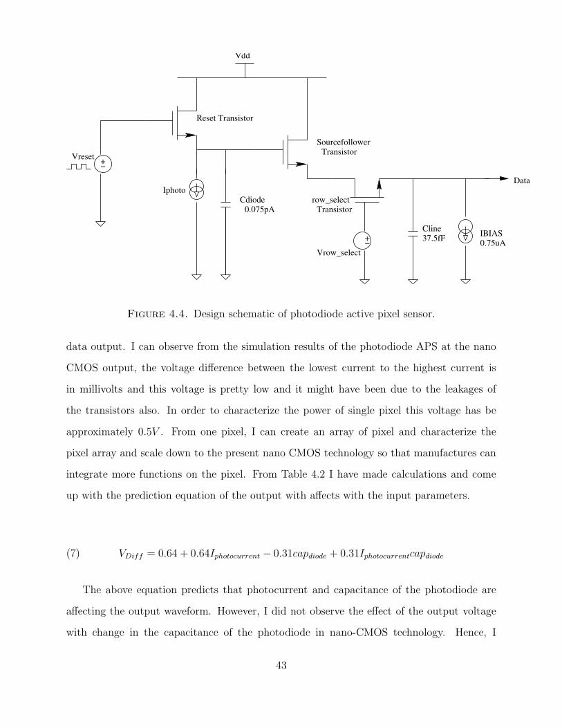
+−
+−
Reset Transistor
SourcefollowerTransistor
Data
Transistorrow_select
Vreset
IphotoCdiode
Vrow_select
Cline IBIAS
0.075pA
37.5fF 0.75uA
Vdd
Figure 4.4. Design schematic of photodiode active pixel sensor.
data output. I can observe from the simulation results of the photodiode APS at the nano
CMOS output, the voltage difference between the lowest current to the highest current is
in millivolts and this voltage is pretty low and it might have been due to the leakages of
the transistors also. In order to characterize the power of single pixel this voltage has be
approximately 0.5V . From one pixel, I can create an array of pixel and characterize the
pixel array and scale down to the present nano CMOS technology so that manufactures can
integrate more functions on the pixel. From Table 4.2 I have made calculations and come
up with the prediction equation of the output with affects with the input parameters.
(7) VDiff = 0.64 + 0.64Iphotocurrent − 0.31capdiode + 0.31Iphotocurrentcapdiode
The above equation predicts that photocurrent and capacitance of the photodiode are
affecting the output waveform. However, I did not observe the effect of the output voltage
with change in the capacitance of the photodiode in nano-CMOS technology. Hence, I
43

Table 4.2. Simulation results for different conditions of inputs.
Iphotodiode CapDiode CapLine IBias V oltage V oltage OutputV oltage
Low Current at High Current at (V low − V high)
pA pF fF µA (50 or 3.75)pA 300 or 22.5 pA Volts
(300 − 50) 1 500 10 2.6232 1.9674 0.6558
(300-50) 1 500 0.75 2.8261 2.1703 0.6558
(300-50) 1 37.5 10 2.6232 1.9674 0.6558
(300-50) 1 37.5 0.75 2.8261 2.1703 6.56E − 01
(300-50) 0.075 500 10 1.337 −5.13E − 01 1.85E + 00
(300-50) 0.075 500 0.75 1.5435 −4.41E − 01 1.98E + 00
(300-50) 0.075 37.5 10 1.337 -5.13E-01 1.85E+00
(300-50) 0.075 37.5 0.75 1.5435 -4.41E-01 1.98E+00
(22.5-3.75) 1 500 10 -1.27E-02 -1.27E-02 0.00E+00
(22.5-3.75) 1 500 0.75 1.86E-01 1.83E-01 2.90E-03
(22.5-3.75) 1 37.5 10 -1.27E-02 -1.27E-02 0.00E+00
(22.5-3.75) 1 37.5 0.75 1.86E-01 1.83E-01 2.90E-03
(22.5-3.75) 0.075 500 10 -1.27E-02 -1.27E-02 0.00E+00
(22.5-3.75) 0.075 500 0.75 1.86E-01 1.83E-01 2.90E-03
(22.5-3.75) 0.075 37.5 10 -1.27E-02 -1.27E-02 0.00E+00
(22.5-3.75) 0.075 37.5 0.75 1.86E-01 1.83E-01 2.90E-03
assume that the photodiode capacitance must be scaled more in order to achieve good
characterization of the photodiode APS.
4.4. Existing Research Work in Active Pixel Sensors
CMOS APS have became a major topic for research and developments in the imaging
systems due to the tremendous usage of APS in consumer applications like mobile phone
44

Figure 4.5. Simulation results for photodiode APS using nano-CMOS.
cameras, webcams, computer video games etc., there is wide area of research going on the
imaging systems in which researchers are trying to explore the CMOS APS with the replace-
ment of matured technology CCD sensors. With the improvements in the CMOS technology,
the APS are also gaining a good research work for scaling the pixel and to integrate more
functions in the APS array. Moreover, this makes manufactures to come up with low power
consumption and low cost of APS array. In this section, I study the ongoing research work
on APS based on the study of current sensors.
45

CMOS APS sensors are dominant for their low power consumption and the integration
of the circuit on camera on chip. They can be operated on a battery provided by the camera
system. So keeping the sensor in silent integration mode during the switch OFF mode of the
digital camera system is needed to order to consume the power on the battery for long used
for digital camera systems. The readout architecture for APS array that is correlated double
sample (CDS) must have low-voltage, low-power with high fill factors. So there are many
designs developing for the scalable CMOS APS for low-voltage and low-power applications.
These designs should include the silent integration mode for low-power consumptions.
Another important aspect of the APS research is the leakages currents due to the pho-
todiode and the shot noise due to the active area of the pixel. The leakages due to the
photodiode should be reduced for correct signal pixel values. Active pixel sensor has 3-4
transistors depending on the application of usage and there are 2-3 transistors which are
active and all the time and may cause leakage currents also. The leakages due to these tran-
sistors also must be reduced. With the developments of the APS sensors building in large
integrated circuit chips may result in the low reliability of the chip. So this needs chips that
can withstand for longer periods. So this can be done by introducing some row and columns
in the integrated circuits. This area of research investigates the fault-tolerance methods,
including redundancy, in APS sensor array [1].
The most important among all research works presented above is to increase the perfor-
mance of APS in reading the pixel value at higher rates. Many designs are proposed for fast
read out techniques and self correcting in the APS array. Hence the active pixels are yet
to be explored in many scientific applications and also consumer applications for high speed
imaging and for extended spectral range.
4.5. Summary
In this chapter, I have discussed about the design parameters of photodiode active pixel
sensors. And also, I talk about the factors that are affecting the output of the active pixel
sensor in voltage swing. The simulation results were presented for AMI 0.6µm technology.
46

The characteristics of the output waveform in voltage mode photodiode active pixel sensor
are also discussed. I have presented a design of experiments for optimizing the APS to
present nano-CMOS technology 45nm in particular.
47

CHAPTER 5
COMPARISON OF PRESENT STATE TECHNOLOGIES OF APS
In the past few years, several active pixel sensor designs have been proposed and explored.
Many kinds of APS were designed on the application of their usage. I present a comparative
evaluation of existing APS in terms of noise, quantum efficiency and etc. Finally, I discuss
all the applications of active pixel sensors in consumer and also scientific applications.
5.1. Developments in APS Technology
The CMOS imagers sensors are targeting high developments in active pixel sensors which
are fabricated standard nano-CMOS technology. Active pixel sensors are made in CMOS
technology have several potentials advantages with the respect to the other sensors in terms
of power, size and flexibility. In last few years, CMOS APS became a major imaging sensor
for the consumer applications. The technology of CMOS APS is cheap and widely available
in the market. This trend is increasing with technology development and showing many
established techniques for commercial systems. Because of their growing ubiquity, there is
a particular need for further development, these aspects of the CMOS APS technology are
required specifically for scientific imaging scientific applications and demand high perfor-
mance CMOS active pixel sensors in terms of low noise, fast read out, and less compact.
CMOS APS are also called as monolithic active pixel sensors (MAPS). The term MAPS is
derived in order to differentiate CMOS APS from hybrid detectors (also called hybrid active
pixel sensors or HAPS). In HAPS the readout circuit has two different substrates which are
proposed for high-energy physics. CMOS APS or monolithic APS being compatible with
CMOS technology have taken several advantages in the recent years. With the shrinking
size of the transistors the CMOS APS can be derived into small pixels or more functions
can be developed in the pixel itself. APS sensors developed in recent years have less power
48

consumption and also good in resisting the high radiation pixel. Upon that, in the recent
developments the APS are said to have several functionalities that can be integrated on the
same chip with the APS sensor arrays. This feature provides APS array as a simplified
system and reduces the cost of the pixel. With APS array the system pixels can be accessed
randomly with fast readout modes or enabling the fast track of the images. APS are very
easy to use except for reading the digital input output (I/O) devices.
The developments in active pixel sensors have gained a very vital role in research work
because of many industrial applications. The main developments of APS are:
(1) Reduction in leakage currents such as dark current, gate leakage.
(2) Increasing dynamic range .
(3) Improvements in the quantum efficiency .
(4) Making APS array read fast.
The first developments can be observed in the industry basis applications [74]. The
expressive developments of CMOS APS Image sensor have made them useful in the science
technology. The first CMOS APS image sensor science application is used for image sensors
in vertex detector in particle physics [71]. After that different technologies of APS are tested
and results are provided for proving 100% efficiency in science application.
With the developments in the CMOS active pixel sensor, they are said to be over 30% of
the market and will go over to 50% in coming years challenging the CCD sensors. This CMOS
APS are also used in the detection of the wide spectrum of electromagnetic applications,
ranging from infrared to UV and low energy X-rays of charged particles. These potential
developments in CMOS APS of different applications will make more developments in the
next coming years.
5.2. Applications of APS Image Sensors
CMOS image sensors have wide applications ranging from consumer applications and
machine vision application to scientific research applications. The market is flourishing by
many other applications like mobile communication applications, wide band applications and
49

also computer networking applications. The capability of CMOS image sensor providing with
low cost, low power consumption, light weight and integrating of pixel with different functions
is allowing market with a substitution to CCD sensors. The CMOS APS applications for
different areas are as follows:
• Commercial and Industrial: Security Cameras, Digital Still Cameras, Camcorders,
webcams for computers, Notebooks and etc..,
• Automotive Applications: Sensors are used as automatic cruise control systems for
vehicles, product quality control, and robot vision.
• Scientific applications: Sensors are used as vertex detectors in particle physics for
tracking the objects and also in planet and biological cell filming.
• Medical Applications: CMOS image sensors with qualities are ideally suited to the
medical market. Low-power use, small package sizes, best-in-class image output,
and uncompromising quality sensor are very much used in medical applications such
as X-rays; Pill cams are used for video gastrointestinal diagnosis. CMOS imaging
technology is providing improved diagnostic capabilities.
• Mobile Applications: Wireless, handheld products that offer a combination of com-
puting, mobile, and imaging capabilities are today’s on-the-going lifestyles. The
video cameras in the mobiles with high resolutions are done by the CMOS APS.
With CMOS APS now it is possible to have up to 2 mega pixel in mobile phones.
• Security Applications: Home security systems require image sensors with high dy-
namic range which are provided by the CMOS image sensors and these are also used
in monitoring all the lighting condition in room.
As discussed above, the developments of CMOS imager size with the reduction sub
micron transistor size may also lead to some disadvantages in CMOS APS sensors, such as
poor sensitivity, high leakage current, and high fixed pattern noise may occur. I need to do
a careful study of all factors affecting the CMOS image sensors so that it will not affect the
performance of the pixel in the image quality. There are some more disadvantages signal
50

cross talk and trade off on the image sensor applications, so I still require more study about
existing CMOS APS.
5.3. Comparative Evaluation of Existing APS
In this section, I summarize all CMOS image sensors technologies. Table 5.1 shows the
comparative evaluations of existing APS technologies. This table gives us a brief perspective
study of the current state-of-art in the CMOS image sensor technologies of all acitve pixel
sensor.
CMOS image sensors mentioned in the table were Passive pixel sensor, CMOS active pixel
sensor, CMOS photogate active pixel sensor, digital pixel sensor. The parameters mentioned
in the table for passive pixel sensor is cited in [31]. This paper discuss about the fixed pattern
noise (FPN) reduction in the passive pixel sensors (PPS). Here the photodiode is used as the
sensing element of PPS. They have used differential correlated doubling amplifier to improve
the performance of mismatching of the transistors. Simulation results in the paper showed
a fill factor of 40%. Here the parasitic current is removed by the differential CDS circuit
which reduces the fill factor.
CMOS active pixel sensor model is same as that of the photodiode active pixel sensor.
This pixel can have 3 or 4 transistors in each pixel depending on the application of usage.
Photodiode APS is commonly used pixel sensor in consumer applications. The parameters
discussed in the table are the simulation results of CMOS APS sensor for nano imaging [19].
This paper designs an APS array of 512 × 550 pixels, each 5 × 5 µm in size. They have
designed a new direct electron imaging sensor for nano imaging and they will having an
impact on the upcoming nano and biological imaging sensors.
CMOS photogate APS has the similar structure of the photodiode active pixel sensor but
the characteristics and the photo sensing elements are different. This pixel also may have 3
or 4 transistors in each pixel depending on the application of usage. Performance analysis
of a color CMOS photogate image sensor has been reported in [5]. They have fabricated
51

Table 5.1. Summary of CMOS sensor technologies.
Sensor Introduced Developer Type Components Technology Pixel Dynamic Sensitivity Fill Pixel Readout
by Size Range Factor FPN Mode
PPS Ickler Recticon Lateral 1 Photodiode 0.6µm 20X20 High 40% 0.1% Analog
[72] Hitchi 1 Transistor CMOS µm2
[20]
CMOS Fossum JPL Lateral 1 Photodiode 0.18µm 5X5 60dB 24 µVe− 100% 4mV Analog
APS [21] /Caltech 3 − 4 transistors µm2 rms
[20]
Photogate Mendis et.al JPL Lateral 1 Photogate 0.8µm 16X16 68dB 35% 0.29% Analog
APS [43] 4 transistors CMOS µm2
[20]
DPS Keinfelder et.al Kodak, Lateral 1 Photodetector 0.35µm 50X50 90dB 20% 0.8% Digital
[35] Cannon HP More transistors µm2
[35]
52

352 × 288 photogate APS in a Lucent technologies of 0.8µm CMOS process with a pixel
dimensions of 16 × 16 µm.
Recently few years ago, DPS was introduced which was discussed in the Chapter 3. This
pixel has built analog-to-digital Converter which read out digital data directly. This pixel
has several advantages compared to the analog image sensors, like passive pixel sensor and
active pixel sensor. The model of DPS which is presented in the table has a programmable
resolution and reconfigurable conversion time using pulse width modulation (PWM) [4]. A
pixel size of 50 by 50 µmt2 of CMOS 0.35 µm process is reported with a dynamic range of
95 as mentioned in the table.. While analyzing the table, I observed that the trend in the
CMOS image sensors technology is decreasing day by day. Hon-Sum Wong presented general
trend in technology and device scaling considerations for CMOS imager sensors [73].
5.4. Summary
In this chapter, I have discussed about the developments and different applications of
APS. I have explored the current state of art in the APS by examining the different types of
pixel that have discussed in the chapter 3. I have discussed different parameters of CMOS
image Sensor factors with the respect to the technology like dynamic range, sensitivity, fill
factor and pixel fixed pattern noise. I observed the technology trend in the CMOS image
sensor according to the performance.
53

CHAPTER 6
SUMMARY AND CONCLUSIONS
A study on the CMOS active pixel sensors is presented in this thesis. The major topics of
this thesis are divided in three parts, which includes the study on the different types of active
pixel sensors discussed in Chapter 3, I have also shown the design and simulations of one of
the commonly used APS that is photodiode APS and one of the optimization method used
to optimize the APS design that is design of experiments (DOE) are presented, but for the
characterization the peak voltage difference between the low light pixel and high light pixel
is low due the leakage in the circuit. Also, I have studied the developments and applications
of APS for consumer and scientific imaging systems. A detailed comparative analysis of
the present CMOS sensor technologies are summarized in a table. I predict that this thesis
serves as guide line for upcoming researchers to work on the APS imaging systems.
Much work has been done in the past five years on CMOS image sensors in which re-
searchers think that it will be the successor of the charged couple devices sensors (CCD).
With the strength of the camera phones in market, overall CMOS APS sensors shipments
exceeded over CCD sensors by nearly 3 times in year the 2005 and the survey reports that
this gap will increase more in the coming future. Consumer applications of the CMOS active
pixel sensors are making researchers to work on less power and optimized sensors.
54

APPENDIX
DEFINITION OF TERMS USED
55

• Dark Current: It is defined as a constant response by produced by the photodetec-
tors such photodiode, photogate, charged couple device etc . . . even when there is
no flow of photons entering the device.
• Dynamic Range: It is defined as the ratio of the saturation to the noise. It is also
defined as the luminosity range of a scene.
• Fill Factor: It is defined has the ratio of the light intensity area of a pixel to its
total area
• Fixed Pattern Noise (FPN): It is noise pattern occurred during the exposure. It is
calculated by the ratio of variance to standard deviation of the image file. Usually
expressed in Vpp or vrms or % (Vrms / saturation level)
• Frame rate: It is measure of number of frames acquired in a second. It measured in
frames/sec.
• Saturation Level: It is defined as the maximum output voltage swing, which is the
difference between the output voltages of low pixel to the high pixel value.
• Sensitivity: It refers to the ability to capture the desired image at a given illumina-
tion.
• Signal to Noise Ratio (SNR): It is defined as the ratio of the saturation level to the
output of the temporal noise in the dark.
• Quantum Efficiency: It is defined as the ratio between the number of generated
electrons and the number of impinging photons.
56

BIBLIOGRAPHY
[1] Active Pixel Sensors Papers: Prof. Glenn H. Chapman, http://www.ensc.sfu.ca/people/faculty/chapman/apspapers.html.
[2] F. Andoh, K. Taketoshi, J. Yamazaki, M. Sagawara, Y. Fujita, K. Mitani, Y. Matuzawa, K. Miyata, and
S. Araki, A 250,000 pixel image sensor with FET amplification at each pixel for high speed television
cameras, IEEE ISSCC (1990), 212–213.
[3] C.H. Aw and B.A. Wooley, A 128x128-pixel standard-CMOS image sensor with electronic shutter, IEEE
Journal of Solid-State Circuits 31 (1996), 1922–1930.
[4] Amine Bermak and Yat-Fong Yung, A DPS array with programmable resolution and reconfigurable
conversion time, IEEE Transactions on Very Large Scale Integration (VLSI) Systems 14 (2006), 15–22.
[5] Andrew J. Blanksby and Marc J. Loinaz, Performance analysis of a color CMOS photogate image
sensor, IEEE Transactions on Electron Devices 47 (2000), 55–64.
[6] Carrier Generation and Recombination, http://www.ece-www.colorado.edu/ bart/book/recomb.html.
[7] S. G. Chamberlain and J. Y. Lee, A novel wide dynamic range silicon photodetector and linear imaging
array, IEEE Tran. Electron Devices 31 (1984), 175.
[8] G. H. Chapman, S. Djaja, D. Y. H. Cheung, Y. Audet, I. Koren, and Z. Koren, A self-correcting active
pixel sensor using hardware and software correction, IEEE Design and Test of Computers 21 (2004),
544–551.
[9] Lin Che-I, Lai Cheng-Hsiao, and Ya-Chin King, A four transistor CMOS active pixel sensor with high
dynamic range operation, Proceedings of IEEE Asia-Pacific Conference on Advanced System Integrated
Circuits (2004), 124 – 127.
[10] Desmond Yu Hin Cheung, CMOS Active Pixel Sensor Designs for Fault Tolerance and Background
Illuminations Subtraction, 2002.
[11] CMOS vs CCD and the Future of Imaging, http://www.kodak.com/US/en/corp/researchDevelopment/technologyFeatures/cmos.shtml.
[12] R. H. Dennard, Field-effect Transistor Memory, US Patent 387286 (1968), no. 3.
[13] A. Dickinson, B. Ackland, E-S. Eid, D. Inglis, and E.R. Fossum, A 256x256 CMOS active pixel image
sensor with motion detection, IEEE ISSCC Tech. Dig (1995), 226–227.
[14] Digital Camera History, http://www.digicamhistory.com/1970s.html.
57

[15] Digital photography Review, http://www.dpreview.com/news/0311/03111901infotrends53mil.asp.
[16] Sima Dimitrijev, Understanding of Semiconductor Devices, 1999.
[17] S. Djaja, G. H. Chapman, D. Y. H. Cheung, and Y. Audet, Implementation and testing of fault-
tolerant photodiode-based active pixel sensor (APS), Proc.International Symposium on Defect and Fault
Tolerance in VLSI Systems (2003), 53–60.
[18] C.A Eldering, M. L. Sylla, and J.A. Eisenach, Is there a Moore’s law for bandwidth, IEEE Communica-
tions Magazine 37 (1999), 117–121.
[19] A CMOS Sensor for Nano-Imaging, Li. Shengdong and S. Kleinfelder and Jin Liang and N. H. Xuong,
IEEE Conference on Nanotechnology 2 (2006), 544–547.
[20] E. R. Fossum, CMOS Image Sensors: Electronic Camera on a Chip, IEEE Transactions on Electron
Devices 44 (1997), 1689–16984.
[21] Eric R. Fossum, Active pixel sensors (APS)- Are CCDs dinosaurs, Proc. SPIE Charged Coupled Devices
and Solid State Optical Sensors III 1900 (1992), no. 1, 2–14.
[22] G. E. Smith G. F. Amelio, M. F. Tompsett, Experimental Verification of the Charge Coupled Device
Concept, Bell System Technical Journal 49 (1970), 593–600.
[23] Abbas El Gamal and Helmy Eltoukhy, CMOS IMAGE SENSORS, IEEE CIRCUITS and DEVICES
MAGAZINE (2005), 8755–3996.
[24] Neil Gershenfeld, The Physics of Information Technology, Cambridge University, 2000.
[25] R. M. Gruidash, T. H. Lee, P. P. K. Lee, D. H. Sackett, C. I. Drowley, M. S. Swenson, L. Arbaugh,
R. Hollstein, F. Shapiro, and S. Domer, A 0.6um CMOS Pinned Photodiode Color Imager Technology,
Technical Digest of IEEE Electron Device Meeting (1997), 927–929.
[26] A.E. Gamal H. Tian, B. Fowler, Analysis of Temporal Noise in CMOS Photodiode Active Pixel Sensor,
IEEE Journal of Solid-State Circuits 36 (2001), 92–101.
[27] T. Hamamoto and K. Aizawa, A computational image sensor with adaptive pixel-based integration time,
IEEE Journal of Solid-State Circuits 36 (2001), 580–585.
[28] R. Hornsey, Design and Fabrication of Integrated Image Sensors (course), Electrical and Computer
Engineering, University of Waterloo, Waterloo, Ontario, Canada (1998).
[29] J. Hynecek, Low-Noise and High-Speed Charge Detection in High Resolution CCD Image Sensors, IEEE
Transactions on Electron Devices 44 (1997), 1679–1688.
[30] O. Yadid-Pecht I. Shcherback, Photoresponse analysis and pixel shape optimization for CMOS active
pixel sensors, IEEE Transactions on Electron Devices 50 (2003), 12–18.
58

[31] C.G. Sodini I.L. Fujimori, Ching-Chun Wang, A 256256 CMOS differential passive pixel imager with
FPN reduction techniques, IEEE Conference of Solid-State Circuits (2000), no. 1, 106–107.
[32] Cadence Design Systems Inc., Spectre circuit simulator user’s guide, 2005.
[33] M. Sawan J. Coulombe and C. Wang, Variable resolution CMOS current mode active pixel sensor, IEEE
International Symposium on Circuits and Systems 5 (2000), 293–296.
[34] K.S. Karim, P. Servati, N. Mohan, A. Nathan, and J.A Rowlands, VHDL-AMS modeling and simulation
of a passive pixel sensor in a-Si:H technology for medical imaging, IEEE International Symposium on
Circuits and Systems 5 (2001), 479–482.
[35] Stuart Kleinfelder, SukHwan Lim, Xinqiao Liu, and Abbas El Gamal, A 10000 frames/s CMOS digital
pixel sensor, IEEE JOURNAL OF SOLID-STATE CIRCUITS 36 (2001), 2049–2059.
[36] A. Krymski, D. Van Blerkom, A. Andersson, N. Bock, B. Mansoorian, and E.R. Fossum, A high speed,
500 frames/s, 1024x1024 CMOS active pixel sensor, IEEE Symposium on VLSI Circuits, Kyoto, Japan,
June (1999), 137–138.
[37] H. I. Kwon, O. J. Kwon, H. Shin, B. G. Park, S. S. Park, and J. D. Lee, The Effects of Deuterium
Annealing on the Reduction of Dark Currents in the CMOS APS, IEEE Tran. Electron Devices 8 (2004),
1346–1349.
[38] Che l Lin, Cheng-Hsiao Lai, and Ya-Chin King, A Four Transistor CMOS Active Pixel Sensor with
High Dynamic Range Operation, IEEE Asia-Pacific Conference on Advanced System Integrated Circuits
(2004), 124– 127.
[39] Dave Litwiller, CCD vs. CMOS: Facts and Fiction, Photonics Spectra (2001).
[40] B. Mansoorian, H.-Y. Yee, S. Huang, and E. Fossum, A 250mW, 60Frames/s 1280x720 pixel 9b CMOS
digital image sensor, IEEE International Solid-State Circuits Conference, San Francisco, CA, USA, Feb
(1999), 312–313.
[41] C. Matsumoto, Startup develops CCD-CMOS hybrid, Electronic Engineering Times (1997).
[42] L.G. McIlrath, S. Vincent, and Peter K. Duane, Design and Analysis of a 512 x 768 Current-Mediated
Active Pixel Array Image Sensor, IEEE Transactions on Electron Devices 4 (1997), 1706–1715.
[43] S. Mendis, S. Kemeny, and E.R. Fossum, A 128x128 CMOS active pixel image sensor for highly integrated
imaging systems, IEEE IEDM Tech. Dig (1993), 583–586.
[44] S. K. Mendis, E. S. Kemeny, C. R. Gee, B. Pain, Q. Kim, and E. R. Fossum, CMOS active pixel image
sensors, Proc. SPIE (1994), 19–29.
59

[45] S.K. Mendis, S.E. Kemeny, R.C. Gee, B. Pain, C.O. Staller, Q. Kim, and E.R. Fossum, CMOS active
pixel image sensors for highly integrated imaging systems, IEEE Journal of Solid-State Circuits 32
(1997), 187–197.
[46] Molecular Expressions Microscopy Primer: Digital Imaging in Optical Microscopy -Interaction of Pho-
tons with Silicon, http://microscopy.fsu.edu/primer/java/digitalimaging/ccd/quantum/index.html.
[47] Molecular Expressions Microscopy Primer: Digital Imaging in Optical Microscopy
Concepts in Digital Imaging Technology Anatomy of a Charge Coupled Device,
http://www.micro.magnet.fsu.edu/primer/digitalimaging/concepts/ccdanatomy.htm.
[48] J. Nakamura, B. Pain, T. Nomoto, T. Nakamura, and E. Fossum, On-focal-plane signal processing for
current-mode active pixel sensors, IEEE Transactions on Electron Devices 44 (1997), 1747–1758.
[49] R. Narendran, A Study of CMOS Cameras, Student Report for Course ELEC 663,Auburn University
(2000).
[50] G.R. Nelson, G.A. Jullien, and O. Yadid-Pecht, CMOS Image Sensor with Watermarking Capabilities,
IEEE International Symposium on Circuits and Systems 5 (2005), 5326–5329.
[51] R.H. Nixon, S.E. Kemeny, B. Pain, C.O. Staller, and E.R. Fossum, 256x256 CMOS active pixel sensor
camera-on-a-chip, IEEE Journal of Solid-State Circuits 31 (1996), 2046–2050.
[52] P. Nobel, Self-Scanned image detector arrays, IEEE Transactions on Electron Devices 15 (1968), 202.
[53] Photodiode Characteristics and Applications, http://www2.physics.utoronto.ca/ astum-
mer/mirror/Projects/Util/.
[54] Review of 20th century progress in electroncs devices, http://www.xcvcorp.com/.
[55] N. Ricquier and B. Dierickx, Pixel structure with logarithmic response for intelligent and flexible imager
architectures, Microelectron. Engineering 19 (1992), 631–634.
[56] H.W. Li R.J. Baker and D.E. Boyce, CMOS Circuit Design, Layout and Simulation, IEEE Press (1998),
78–79.
[57] C. H. Sequin, Interlacing in Charge-Coupled Imaging Devices, IEEE Transactions on Electron Devices
20 (1973), 535–541.
[58] C. H. Sequin, D. Sealer, W. Bertram, R. Buckley, F. Morris, T. Shankoff, and M. Tompsett, Charge-
coupled image-sensing devices using three levels of polysilicon, Solid-State Circuits Conference. Digest
of Technical Papers. 1974 IEEE International 17 (1974).
[59] C.H. Sequin and M.F. Tompsett, Charge Transfer Devices, Advances in Electronics and Electron Physics,
Supplement 8, (1975).
60

[60] Y. Shih and C. Wu, The design of high-performance 128x128 CMOS image sensors using new current-
readout techniques, IEEE International Symposium on Circuits and Systems (1999), 168–171.
[61] Yu-Chuan Shih and Chung-Yu Wu, An optimized CMOS pseudo-active-pixel-sensor structure for low-
dark-current imager applications, IEEE International Symposium on Circuits and Systems (2003), 25–
28.
[62] G. E. Smith, Charge Coupled Memory with Storage Sites, US Patent 3654 (1972), no. 1, 2–14.
[63] SuperCCD, http://www.fujifilm.co.uk/digital/popups/superccd.html.
[64] T.N. Swe and K.S. Yeo, An Accurate Photodiode Model for DC and High Frequency SPICE Circuit Sim-
ulation, Tech Proc. of the 2001 International Conference on Modelling and Simulation of Microsystems
(2001), 362–365.
[65] S. M. Sze, Pyhsics of Semiconductor Devices, John Wiley, 1981.
[66] Technology Review of charged Couple Device and CMOS Based Electronics Imagers,
http://www.eecg.utoronto.ca/ kphang/papers1.htm.
[67] A. Theuwissen, Building a Better Mousetrap: Modified CMOS processes improve sensor performance,
SPIE’s OE Magazine (2001), 29–32.
[68] Hui Tian, Xinqiao Liu, SukHwan Lim, Stuart Kleinfelder, and Abbas El Gamal, Active Pixel Sensors
Fabricated in a Standard 0.18 um CMOS Technology, Proc. SPIE, Electronics Imaging (2001), 441–449.
[69] Toshiba Presents 3.2-Megapixel and 2.0-Megapixel CMOS Image Sensor Lineup ,
http://www.news.soft32.com.
[70] J.-L. Trpanier, M. Sawan, Y. Audet, and J. Coulombe, A Wide Dynamic Range CMOS Digital Pixel
Sensor, Symposium on Circuits and Systems (2002), 437–440.
[71] R. Turchetta, J. D. Berst, B. Casadei, G. Claus, C. Colledani, and W. Dulinski, A monolithic active
pixel sensor for charged particle tracking and imaging using standard VLSI CMOS technology, Nuclear
Instruments and Methods (2001), 677–689.
[72] G. P. Weckler, Operation of p-n Junction Photodetectors in a Photon Flux Integration Mode, IEEE
Journal of Solid-State Circuits SC-2 (1967), 65–73.
[73] Hon-Sum Wong, Technology and device scaling considerations for CMOS imagers, IEEE Transactions
on Electron Devices 43 (1996), 2131–2142.
[74] S.-G. Wuu and et al, High Performance 0.25 m CMOS Color Imager Technology with Non-silicide
Source/Drain Pixel, International Electron Devices Meeting (2000).
[75] O. Yadid-Pecht, R. Ginosar, and Y. Diamand, A random access photodiode array for intelligent image
capture, IEEE Journal of Solid-State Circuits 26 (1991), 1116–1122.
61

[76] , A random access photodiode array for intelligent image capture, IEEE J. Solid-State Circuits
26 (1991), 1116–1122.
[77] Orly Yadid-Pecht and Ralph Etienne-Cummings, CMOS Imagers: From Phototransduction to Image
Processing, Kluwer Academic Publishers, 2004.
[78] K. Yonemoto, H. Sumi, R. Suzuki, and T. Ueno, A CMOS image sensor with a simple FPN-reduction
technology and a hole accumulated diode, IEEE International Solid-State Circuits Conference, San Fran-
cisco, CA, USA, Feb (2000), 102–103.
[79] Z. Zhou, B. Pain, and E.R. Fossum, CMOS active pixel sensor with on-chip successive approximation
analog-to-digital converter, IEEE Transactions on Electron Devices 44 (1997), 1759–1763.
62