cmos 16-bit single chip microcontroller … · devices s1 c 17xxx f 00e1 packing specifications 00...
TRANSCRIPT

CMOS 16-BIT SINGLE CHIP MICROCONTROLLER
S1C17803Technical Manual
Rev.1.1

NOTICE
No part of this material may be reproduced or duplicated in any form or by any means without the written permission of Seiko Epson. Seiko Epson reserves the right to make changes to this material without notice. Seiko Epson does not assume any liability of any kind arising out of any inaccuracies contained in this material or due to its application or use in any product or circuit and, further, there is no representation that this material is applicable to products requiring high level reliability, such as, medical products. Moreover, no license to any intellectual property rights is granted by implication or otherwise, and there is no representation or warranty that anything made in accordance with this material will be free from any patent or copyright infringement of a third party. This material or portions thereof may contain technology or the subject relating to strategic products under the control of the Foreign Exchange and Foreign Trade Law of Japan and may require an export license from the Ministry of Economy, Trade and Industry or other approval from another government agency.
All brands or product names mentioned herein are trademarks and/or registered trademarks of their respective companies.This product uses SuperFlash® technology licensed from Silicon Storage Technology, Inc.
© SEIKO EPSON CORPORATION 2011, All rights reserved.

DevicesS1 C 17xxx F 00E1
Packing specifications00 : Besides tape & reel0A : TCP BL 2 directions0B : Tape & reel BACK0C : TCP BR 2 directions0D : TCP BT 2 directions0E : TCP BD 2 directions0F : Tape & reel FRONT0G: TCP BT 4 directions0H : TCP BD 4 directions0J : TCP SL 2 directions0K : TCP SR 2 directions0L : Tape & reel LEFT0M: TCP ST 2 directions0N : TCP SD 2 directions0P : TCP ST 4 directions0Q: TCP SD 4 directions0R : Tape & reel RIGHT99 : Specs not fixed
Specification
PackageD: die form; F: QFP, B: BGA
Model number
Model nameC: microcomputer, digital products
Product classificationS1: semiconductor
Development toolsS5U1 C 17000 H2 1
Packing specifications 00: standard packing
Version 1: Version 1
Tool typeHx : ICEDx : Evaluation boardEx : ROM emulation boardMx: Emulation memory for external ROMTx : A socket for mounting
Cx : Compiler packageSx : Middleware package
Corresponding model number17xxx: for S1C17xxx
Tool classification C: microcomputer use
Product classification S5U1: development tool for semiconductor products
00
00
Configuration of product number

CONTENTS
S1C17803 TECHNICAL MANUAL Seiko Epson Corporation i
– Contents –
1 Overview ........................................................................................................................1-11.1 Features ...........................................................................................................................1-1
1.2 Block Diagram ..................................................................................................................1-7
1.3 Pin Descriptions ...............................................................................................................1-81.3.1 Pin Arrangement ................................................................................................1-81.3.2 Pin Functions ....................................................................................................1-101.3.3 Input/Output Cells and Input/Output Characteristics ........................................1-161.3.4 Package ............................................................................................................1-181.3.5 Thermal Resistance of the Package .................................................................1-19
2 CPU ................................................................................................................................2-12.1 Features of the S1C17 Core ............................................................................................2-1
2.2 CPU Registers .................................................................................................................2-2
2.3 Instruction Set ..................................................................................................................2-2
2.4 Reading PSR ...................................................................................................................2-5
2.5 Processor Information ......................................................................................................2-6
3 Memory Map and Bus ..................................................................................................3-13.1 Flash Area ........................................................................................................................3-2
3.2 IRAM/IVRAM Area ...........................................................................................................3-2
3.3 BBRAM Area ....................................................................................................................3-2
3.4 Internal Peripheral Area ...................................................................................................3-2
3.5 S1C17 Core I/O Area .......................................................................................................3-3
3.6 Internal Bus ......................................................................................................................3-4
3.7 Access Cycle ....................................................................................................................3-4
4 Power Supply ................................................................................................................4-14.1 Power Supply Pins ...........................................................................................................4-1
4.2 Operating Voltage (LVDD) ..................................................................................................4-3
4.3 I/O Interface Voltages (BUSIO_VDD, IO1_VDD, IO2_VDD) .................................................4-3
4.4 Power Supply for RTC (RTCVDD) .....................................................................................4-3
4.5 Power Supply for Analog Circuits (AVDD) .........................................................................4-3
4.6 Internal Voltage Regulator ................................................................................................4-3
4.7 Precautions on Power Supply ..........................................................................................4-4
5 Reset and NMI ...............................................................................................................5-15.1 Initial Reset ......................................................................................................................5-1
5.1.1 #RESET Pin .......................................................................................................5-15.1.2 Resetting by the Watchdog Timer ......................................................................5-15.1.3 Initial Reset Sequence .......................................................................................5-15.1.4 Initial Reset Status ............................................................................................5-25.1.5 Precautions to be Taken during Initial Reset ......................................................5-2
5.2 NMI Input .........................................................................................................................5-35.2.1 #NMI Pin ............................................................................................................5-35.2.2 NMI by the Watchdog Timer ...............................................................................5-35.2.3 NMI Input Noise Filter ........................................................................................5-3
6 Clock Management Unit (CMU) ...................................................................................6-16.1 CMU Module Overview ....................................................................................................6-1
6.2 CMU Pins .........................................................................................................................6-2

CONTENTS
ii Seiko Epson Corporation S1C17803 TECHNICAL MANUAL
6.3 Oscillators ........................................................................................................................6-26.3.1 OSC3 Oscillator Circuit ......................................................................................6-26.3.2 OSC1 Oscillator Circuit ......................................................................................6-3
6.4 System Clock Settings .....................................................................................................6-46.4.1 System Clock Source Selection .........................................................................6-46.4.2 System Clock Frequency Setting .......................................................................6-5
6.5 Clock Supply Control ........................................................................................................6-56.5.1 Core Clock (CCLK) ............................................................................................6-56.5.2 Bus Clock (BCLK) ..............................................................................................6-56.5.3 Peripheral Module Clocks (PCLK_SOC, PCLK1, PCLK2) .................................6-66.5.4 LCDC Module Clock (LCLK) ..............................................................................6-7
6.6 Clock External Output (CMU_CLK) ..................................................................................6-8
6.7 Standby Modes ................................................................................................................6-86.7.1 HALT Mode ........................................................................................................6-86.7.2 SLEEP Mode .....................................................................................................6-8
6.8 Control Register Details ...................................................................................................6-9Clock Source Select Register (CMU_OSCSRC) ....................................................................... 6-9Oscillation Control Register (CMU_OSCCTL) .......................................................................... 6-10Noise Filter Enable Register (CMU_NFEN) ............................................................................. 6-11LCDC Clock Setup Register (CMU_LCLK) .............................................................................. 6-11Clock Control Register (CMU_CLKCTL) .................................................................................. 6-12System Clock Division Ratio Select Register (CMU_SYSCLKDIV) ......................................... 6-14CMU_CLK Select Register (CMU_CMUCLK) .......................................................................... 6-14MAC Wait Cycle Select Register (MAC_WAIT) ........................................................................ 6-15CMU Write Protect Register (CMU_PROTECT) ....................................................................... 6-15
7 Prescaler (PSC) .............................................................................................................7-17.1 PSC Module Overview .....................................................................................................7-1
7.2 Control Register Details ...................................................................................................7-1PSC Ch.0 Control Register (PSC_CTL0) .................................................................................. 7-2PSC Ch.1–2 Control Register (PSC_CTL1) .............................................................................. 7-2
8 Clock Generator (CLG) .................................................................................................8-18.1 CLG Module Overview .....................................................................................................8-1
8.2 16-bit Timer with Fine Mode (CLG_T16FU0) ...................................................................8-28.2.1 CLG_T16FU0 Overview .....................................................................................8-28.2.2 Count Clock .......................................................................................................8-28.2.3 Count Mode .......................................................................................................8-38.2.4 Reload Register and Underflow Period ..............................................................8-38.2.5 Timer Reset .......................................................................................................8-38.2.6 Run/Stop Control ...............................................................................................8-48.2.7 CLG_T16FU0 Output Signal ..............................................................................8-48.2.8 Fine Mode ..........................................................................................................8-58.2.9 CLG_T16FU0 Interrupt ......................................................................................8-68.2.10 Details of Control Registers .............................................................................8-6
CLG_T16FU0 Input Clock Select Register (CLG_T16FU0_CLK) ............................................. 8-6CLG_T16FU0 Reload Data Register (CLG_T16FU0_TR) ........................................................ 8-7CLG_T16FU0 Counter Data Register (CLG_T16FU0_TC) ....................................................... 8-7CLG_T16FU0 Control Register (CLG_T16FU0_CTL) ............................................................... 8-7CLG_T16FU0 Interrupt Control Register (CLG_T16FU0_INT) ................................................. 8-9
8.3 8-bit Timer (CLG_T8I) .....................................................................................................8-108.3.1 CLG_T8I Overview ...........................................................................................8-108.3.2 Count Clock ......................................................................................................8-108.3.3 Count Mode ......................................................................................................8-118.3.4 Reload Register and Underflow Period .............................................................8-11

CONTENTS
S1C17803 TECHNICAL MANUAL Seiko Epson Corporation iii
8.3.5 Timer Reset ......................................................................................................8-118.3.6 Run/Stop Control ..............................................................................................8-128.3.7 CLG_T8I Output Signal ....................................................................................8-128.3.8 CLG_T8I Interrupt .............................................................................................8-138.3.9 Details of Control Registers ..............................................................................8-13
CLG_T8I Input Clock Select Register (CLG_T8I_CLK) ............................................................ 8-13CLG_T8I Reload Data Register (CLG_T8I_TR) ....................................................................... 8-14CLG_T8I Counter Data Register (CLG_T8I_TC) ..................................................................... 8-14CLG_T8I Control Register (CLG_T8I_CTL) ............................................................................. 8-14CLG_T8I Interrupt Control Register (CLG_T8I_INT) ................................................................ 8-15
9 Real-Time Clock (RTC) .................................................................................................9-19.1 RTC Module Overview .....................................................................................................9-1
9.2 RTC Counters ..................................................................................................................9-2
9.3 RTC Control .....................................................................................................................9-49.3.1 Operating Clock Control .....................................................................................9-49.3.2 RTC Initial Sequence .........................................................................................9-49.3.3 Counter Settings ................................................................................................9-59.3.4 Start/Stop and Software Reset ..........................................................................9-59.3.5 Counter Hold and Busy Flag ..............................................................................9-59.3.6 30-second Correction ........................................................................................9-6
9.4 RTC Interrupts ..................................................................................................................9-7
9.5 WAKEUP and #STBY Pins ...............................................................................................9-8
9.6 Details of Control Registers ............................................................................................9-10RTC Interrupt Status Register (RTC_INTSTAT) ....................................................................... 9-11RTC Interrupt Mode Register (RTC_INTMODE) ...................................................................... 9-11RTC Control 0 Register (RTC_CNTL0) .................................................................................... 9-12RTC Control 1 Register (RTC_CNTL1) .................................................................................... 9-13RTC Second Register (RTC_SEC) ........................................................................................... 9-14RTC Minute Register (RTC_MIN) ............................................................................................. 9-14RTC Hour Register (RTC_HOUR) ............................................................................................ 9-15RTC Day Register (RTC_DAY) ................................................................................................. 9-15RTC Month Register (RTC_MONTH) ....................................................................................... 9-15RTC Year Register (RTC_YEAR) .............................................................................................. 9-16RTC Days of Week Register (RTC_WEEK).............................................................................. 9-16RTC Wakeup Configuration Register (RTC_WAKEUP) ............................................................ 9-17RTC Wait Control Register (RTC_WAIT) .................................................................................. 9-17
10 Flash Controller (FLASHC) .......................................................................................10-110.1 FLASHC Module Overview ...........................................................................................10-1
10.2 Flash Memory Map .......................................................................................................10-2
10.3 Programming the Flash Memory ...................................................................................10-210.3.1 Chip Erase Procedure.....................................................................................10-310.3.2 Sector Erase Procedure..................................................................................10-410.3.3 Flash Programming Procedure .......................................................................10-6
10.4 Read Access Control ...................................................................................................10-7
10.5 HIDE mode ....................................................................................................................10-7
10.6 Control Register Details ................................................................................................10-8FLASHC Control Register (FLASH_CTL)................................................................................. 10-8FLASHC Sector Address Register (FLASH_ADDR) ............................................................... 10-10FLASHC Wait Register (FLASH_WAIT) .................................................................................. 10-11FLASHC Protect Register (FLASH_PROT) ............................................................................. 10-11
11 SRAM Controller (SRAMC) .......................................................................................11-111.1 SRAMC Module Overview ............................................................................................11-1
11.2 SRAMC Pins .................................................................................................................11-1

CONTENTS
iv Seiko Epson Corporation S1C17803 TECHNICAL MANUAL
11.3 SRAMC Operating Clock ...............................................................................................11-1
11.4 External Memory Area ..................................................................................................11-211.4.1 Chip Enable Signals ........................................................................................11-211.4.2 Area Condition Settings ..................................................................................11-2
11.5 Connection of External Devices and Bus Operation .....................................................11-411.5.1 Connecting External Devices .........................................................................11-411.5.2 Data Configuration in Memory ........................................................................11-411.5.3 External Bus Operation ...................................................................................11-5
11.6 Bus Access Timing Chart ..............................................................................................11-611.6.1 SRAM Read/Write Timings with No External #WAIT ......................................11-611.6.2 SRAM Read/Write Timings with External #WAIT ............................................11-811.6.3 SRAM Burst Read Timing ...............................................................................11-9
11.7 Control Register Details ................................................................................................11-9SRAMC Wait Cycle Configuration Register (SRAMC_WT) ...................................................... 11-9SRAMC Device Size Configuration Register (SRAMC_SIZE) ................................................. 11-10SRAMC Device Mode Configuration Register (SRAMC_MOD) .............................................. 11-10SRAMC Burst Read Control Register (SRAMC_RDBST) ....................................................... 11-11SRAMC #CE1 Bus Clock Division Register (SRAMC_CE1DIV) ............................................. 11-12
11.8 Precautions ..................................................................................................................11-12
12 Interrupt Controller (ITC) ..........................................................................................12-112.1 ITC Module Overview ....................................................................................................12-1
12.2 Vector Table ...................................................................................................................12-2Vector Table Address Low/High Registers (MISC_TTBRL, MISC_TTBRH) ............................. 12-3
12.3 Control of Maskable Interrupts ......................................................................................12-312.3.1 Interrupt Control Bits in Peripheral Modules ...................................................12-312.3.2 ITC Interrupt Request Processing ..................................................................12-412.3.3 Interrupt Processing by the S1C17 Core ........................................................12-4
12.4 NMI ................................................................................................................................12-5
12.5 Software Interrupts ........................................................................................................12-5
12.6 HALT and SLEEP Mode Cancellation ...........................................................................12-5
12.7 Control Register Details ................................................................................................12-6Interrupt Level Setup Register 0 (ITC_LV0) .............................................................................. 12-6Interrupt Level Setup Register 1 (ITC_LV1) .............................................................................. 12-6Interrupt Level Setup Register 2 (ITC_LV2) .............................................................................. 12-7Interrupt Level Setup Register 3 (ITC_LV3) .............................................................................. 12-7Interrupt Level Setup Register 4 (ITC_LV4) .............................................................................. 12-7Interrupt Level Setup Register 5 (ITC_LV5) .............................................................................. 12-7Interrupt Level Setup Register 6 (ITC_LV6) .............................................................................. 12-8Interrupt Level Setup Register 7 (ITC_LV7) .............................................................................. 12-8Interrupt Level Setup Register 8 (ITC_LV8) .............................................................................. 12-8Interrupt Level Setup Register 9 (ITC_LV9) .............................................................................. 12-8
13 DMA Controller (DMAC) ............................................................................................13-113.1 DMAC Module Overview ...............................................................................................13-1
13.2 DMAC Operating Clock .................................................................................................13-1
13.3 Programming Control Information .................................................................................13-213.3.1 Setting the Base Address ...............................................................................13-213.3.2 Control Information .........................................................................................13-213.3.3 Auto-Reload Data ...........................................................................................13-6
13.4 DMAC Invocation ..........................................................................................................13-6
13.5 Operation of DMAC .......................................................................................................13-713.5.1 Single Transfer Mode ......................................................................................13-713.5.2 Successive Transfer Mode ..............................................................................13-9

CONTENTS
S1C17803 TECHNICAL MANUAL Seiko Epson Corporation v
13.6 DMAC Interrupt ............................................................................................................13-11
13.7 Control Register Details ...............................................................................................13-11DMAC General Control Register (DMA_CTL) ......................................................................... 13-11DMAC Control Table Base Address Low/High Registers (DMA_TBL_BASEL/H) ................... 13-12DMAC Interrupt Enable Register (DMA_IE) ............................................................................ 13-13DMAC Trigger Select Register (DMA_TRG_SEL) ................................................................... 13-13DMAC Trigger Flag Register (DMA_TRG_FLG) ...................................................................... 13-14DMAC End-of-Transfer Flag Register (DMA_END_FLG) ........................................................ 13-14DMAC Running Status Register (DMA_RUN_STA) ................................................................ 13-15DMAC Pause Status Register (DMA_PAUSE_STA) ................................................................ 13-15DMAC Data Buffer Low/High Registers (DMA_DATA_BUFL/H) .............................................. 13-15
14 8-bit Programmable Timers (T8F) .............................................................................14-114.1 T8F Module Overview ...................................................................................................14-1
14.2 Count Clock ...................................................................................................................14-2
14.3 Count Mode ...................................................................................................................14-2
14.4 Reload Data Register and Underflow Cycle ..................................................................14-2
14.5 Timer Reset ...................................................................................................................14-3
14.6 RUN/STOP Control .......................................................................................................14-3
14.7 T8F Output Signals .......................................................................................................14-4
14.8 Fine Mode .....................................................................................................................14-4
14.9 T8F Interrupts ................................................................................................................14-5
14.10 Control Register Details ..............................................................................................14-6T8F Ch.x Input Clock Select Registers (T8F_CLKx) ................................................................ 14-6T8F Ch.x Reload Data Registers (T8F_TRx) ........................................................................... 14-7T8F Ch.x Counter Data Registers (T8F_TCx) ......................................................................... 14-7T8F Ch.x Control Registers (T8F_CTLx) ................................................................................. 14-7T8F Ch.x Interrupt Control Registers (T8F_INTx) .................................................................... 14-9
15 16-bit PWM Timer (T16A)...........................................................................................15-115.1 T16A Module Overview .................................................................................................15-1
15.2 T16A Input/Output Pins .................................................................................................15-2
15.3 Count Clock ...................................................................................................................15-2
15.4 T16A Operating Modes .................................................................................................15-315.4.1 Comparator Mode and Capture Mode ............................................................15-315.4.2 Repeat Mode and One-Shot Mode .................................................................15-4
15.5 Counter Control ............................................................................................................15-415.5.1 Counter Reset .................................................................................................15-415.5.2 Counter RUN/STOP Control ...........................................................................15-415.5.3 Reading Counter Values .................................................................................15-515.5.4 Timing Charts..................................................................................................15-5
15.6 Timer Output Control .....................................................................................................15-6
15.7 T16A Interrupts ..............................................................................................................15-7
15.8 Control Register Details ................................................................................................15-8T16A Counter Control Register (T16A_CTL) ........................................................................... 15-9T16A Counter Data Register (T16A_TC) ................................................................................ 15-10T16A Comparator/Capture Control Register (T16A_CCCTL) ................................................. 15-10T16A Comparator/Capture A Data Register (T16A_CCA) ...................................................... 15-12T16A Comparator/Capture B Data Register (T16A_CCB) ...................................................... 15-13T16A Comparator/Capture Interrupt Enable Register (T16A_IEN) ......................................... 15-13T16A Comparator/Capture Interrupt Flag Register (T16A_IFLG) ........................................... 15-14
16 16-bit Audio PWM Timer (T16P) ................................................................................16-116.1 T16P Module Overview .................................................................................................16-1
16.2 T16P Input/Output Pins .................................................................................................16-2

CONTENTS
vi Seiko Epson Corporation S1C17803 TECHNICAL MANUAL
16.3 Setting T16P Operating Conditions ...............................................................................16-216.3.1 Count Clock ....................................................................................................16-216.3.2 PCM Data Configuration .................................................................................16-316.3.3 Operating Mode Selection ..............................................................................16-316.3.4 PWM Output Condition Settings .....................................................................16-4
16.4 Control and T16P Operations ........................................................................................16-416.4.1 Resetting T16P ...............................................................................................16-416.4.2 Run/Stop Control ............................................................................................16-516.4.3 Setting Compare Data ....................................................................................16-516.4.4 Volume Control ................................................................................................16-616.4.5 Counter Value .................................................................................................16-616.4.6 Timing Charts..................................................................................................16-6
16.5 T16P Interrupts and DMA ..............................................................................................16-816.5.1 Interrupts .........................................................................................................16-816.5.2 DMA Transfer ..................................................................................................16-9
16.6 Control Register Details ................................................................................................16-9T16P Compare A Buffer Register (T16P_A) ............................................................................ 16-9T16P Compare B Buffer Register (T16P_B) ........................................................................... 16-10T16P Counter Data Register (T16P_CNT_DATA) ................................................................... 16-10T16P Volume Control Register (T16P_VOL_CTL) .................................................................. 16-11T16P Control Register (T16P_CTL) ........................................................................................ 16-11T16P Running Control Register (T16P_RUN) ......................................................................... 16-13T16P Internal Clock Control Register (T16P_CLK) ................................................................. 16-14T16P Interrupt Control Register (T16P_INT) ........................................................................... 16-14
17 Watchdog Timer (WDT) ..............................................................................................17-117.1 WDT Module Overview .................................................................................................17-1
17.2 WDT Input/Output Pins .................................................................................................17-1
17.3 WDT Operating Clock ..................................................................................................17-2
17.4 Control of the Watchdog Timer ......................................................................................17-217.4.1 Setting Up the Watchdog Timer ......................................................................17-217.4.2 Starting/Stopping the Watchdog Timer ..........................................................17-317.4.3 Resetting the Watchdog Timer .......................................................................17-317.4.4 Operation in Standby Mode ............................................................................17-317.4.5 Clock Output of the Watchdog Timer .............................................................17-317.4.6 External NMI Output .......................................................................................17-4
17.5 Control Register Details ................................................................................................17-4WDT Write Protect Register (WD_WP) .................................................................................... 17-4WDT Enable and Setup Register (WD_EN) ............................................................................. 17-5WDT Comparison Data L/H Registers (WD_CMP_L, WD_CMP_H) ........................................ 17-6WDT Count Data L/H Registers (WD_CNT_L, WD_CNT_H) ................................................... 17-6WDT Control Register (WD_CTL) ............................................................................................ 17-6
18 UART ...........................................................................................................................18-118.1 UART Module Overview ................................................................................................18-1
18.2 UART Input/Output Pins ................................................................................................18-1
18.3 Transfer Clock ................................................................................................................18-2
18.4 Transfer Data Settings ...................................................................................................18-2
18.5 Data Transfer Control ....................................................................................................18-3
18.6 Receive Errors...............................................................................................................18-5
18.7 UART Interrupts ............................................................................................................18-6
18.8 IrDA Interface ................................................................................................................18-6
18.9 Control Register Details ................................................................................................18-8UART Status Registers (UART_ST) ......................................................................................... 18-8

CONTENTS
S1C17803 TECHNICAL MANUAL Seiko Epson Corporation vii
UART Transmit Data Registers (UART_TXD) ........................................................................... 18-9UART Receive Data Registers (UART_RXD) .......................................................................... 18-10UART Mode Registers (UART_MOD) ..................................................................................... 18-10UART Control Registers (UART_CTL) .................................................................................... 18-11UART Expansion Registers (UART_EXP) ............................................................................... 18-12
19 Universal Serial Interface (USI) ................................................................................19-119.1 USI Module Overview ..................................................................................................19-1
19.2 USI Pins ........................................................................................................................19-2
19.3 USI Clock Sources ........................................................................................................19-2
19.4 USI Module Settings ....................................................................................................19-319.4.1 USI Module Software Reset ............................................................................19-319.4.2 Interface Mode ................................................................................................19-419.4.3 General Settings for All Interface Modes ........................................................19-419.4.4 Settings for UART Mode ................................................................................19-419.4.5 Settings for SPI Mode ....................................................................................19-519.4.6 Settings for I2C Mode .....................................................................................19-6
19.5 Data Transfer Control ....................................................................................................19-619.5.1 Data Transfer in UART Mode ..........................................................................19-619.5.2 Data Transfer in SPI Mode ..............................................................................19-819.5.3 Data Transfer in I2C Mode ...............................................................................19-9
19.6 Receive Errors..............................................................................................................19-21
19.7 USI Interrupts and DMA ...............................................................................................19-2219.7.1 Interrupts in UART Mode ...............................................................................19-2219.7.2 Interrupts in SPI Mode ...................................................................................19-2319.7.3 Interrupts in I2C Master Mode ........................................................................19-2319.7.4 Interrupts in I2C Slave Mode ..........................................................................19-2419.7.5 111DMA Transfer ...........................................................................................19-25
19.8 Control Register Details ...............................................................................................19-25USI Ch.x Global Configuration Registers (USI_GCFGx) ........................................................ 19-26USI Ch.x Transmit Data Buffer Registers (USI_TDx) .............................................................. 19-26USI Ch.x Receive Data Buffer Registers (USI_RDx) .............................................................. 19-27USI Ch.x UART Mode Configuration Registers (USI_UCFGx) ............................................... 19-27USI Ch.x UART Mode Interrupt Enable Registers (USI_UIEx) ............................................... 19-28USI Ch.x UART Mode Interrupt Flag Registers (USI_UIFx) .................................................... 19-28USI Ch.x SPI Master/Slave Mode Configuration Registers (USI_SCFGx) ............................. 19-30USI Ch.x SPI Master/Slave Mode Interrupt Enable Registers (USI_SIEx) ............................. 19-31USI Ch.x SPI Master/Slave Mode Interrupt Flag Registers (USI_SIFx) .................................. 19-31USI Ch.x I2C Master Mode Trigger Registers (USI_IMTGx).................................................... 19-32USI Ch.x I2C Master Mode Interrupt Enable Registers (USI_IMIEx) ...................................... 19-33USI Ch.x I2C Master Mode Interrupt Flag Registers (USI_IMIFx) ........................................... 19-34USI Ch.x I2C Slave Mode Trigger Registers (USI_ISTGx) ...................................................... 19-35USI Ch.x I2C Slave Mode Interrupt Enable Registers (USI_ISIEx) ......................................... 19-36USI Ch.x I2C Slave Mode Interrupt Flag Registers (USI_ISIFx) ............................................. 19-36
19.9 Precautions ..................................................................................................................19-38
20 I2C Master (I2CM) .......................................................................................................20-120.1 I2CM Module Overview .................................................................................................20-1
20.2 I2CM Input/Output Pins .................................................................................................20-1
20.3 I2C Master Clock ...........................................................................................................20-1
20.4 Settings Before Data Transfer .......................................................................................20-2
20.5 Data Transfer Control ....................................................................................................20-2
20.6 I2CM Interrupts .............................................................................................................20-6
20.7 Control Register Details ................................................................................................20-7I2C Master Enable Register (I2CM_EN) ................................................................................... 20-7

CONTENTS
viii Seiko Epson Corporation S1C17803 TECHNICAL MANUAL
I2C Master Control Register (I2CM_CTL) ................................................................................. 20-7I2C Master Data Register (I2CM_DAT) ..................................................................................... 20-8I2C Master Interrupt Control Register (I2CM_ICTL) ................................................................ 20-10
21 I2C Slave (I2CS) ..........................................................................................................21-121.1 I2CS Module Overview .................................................................................................21-1
21.2 I2CS Input/Output Pins .................................................................................................21-1
21.3 I2C Slave Clock .............................................................................................................21-2
21.4 Initializing I2CS .............................................................................................................21-221.4.1 Reset ..............................................................................................................21-221.4.2 Setting Slave Address .....................................................................................21-221.4.3 Optional Functions ..........................................................................................21-2
21.5 Data Transfer Control ....................................................................................................21-3
21.6 I2CS Interrupts ..............................................................................................................21-8
21.7 Control Register Details ................................................................................................21-9I2C Slave Transmit Data Register (I2CS_TRNS) ...................................................................... 21-9I2C Slave Receive Data Register (I2CS_RECV) ..................................................................... 21-10I2C Slave Address Setup Register (I2CS_SADRS) ................................................................. 21-10I2C Slave Control Register (I2CS_CTL)................................................................................... 21-10I2C Slave Status Register (I2CS_STAT) .................................................................................. 21-12I2C Slave Access Status Register (I2CS_ASTAT) ................................................................... 21-14I2C Slave Interrupt Control Register (I2CS_ICTL) ................................................................... 21-15
22 I2S ................................................................................................................................22-122.1 I2S Module Overview .....................................................................................................22-1
22.2 I2S Output Pins ..............................................................................................................22-1
22.3 I2S Module Operating Clock ..........................................................................................22-2
22.4 Setting the I2S Module ..................................................................................................22-2
22.5 Data Output Control ......................................................................................................22-6
22.6 I2S Interrupt and DMA ...................................................................................................22-922.6.1 Interrupts .........................................................................................................22-922.6.2 DMA Transfer .................................................................................................22-10
22.7 Control Register Details ...............................................................................................22-11I2S Control Register (I2S_CTL) ............................................................................................... 22-11I2S Master Clock Division Ratio Register (I2S_DV_MCLK) ..................................................... 22-14I2S Audio Clock Division Ratio Register (I2S_DV_AUDIO_CLK) ............................................. 22-14I2S Start/Stop Register (I2S_START) ...................................................................................... 22-16I2S FIFO Status Register (I2S_FIFO_STAT) ............................................................................ 22-17I2S Interrupt Control Register (I2S_INT) .................................................................................. 22-17I2S FIFO Register (I2S_FIFO) ................................................................................................. 22-19
22.8 Setting the I2S Clocks ..................................................................................................22-19
23 Remote Controller (REMC) .......................................................................................23-123.1 REMC Module Overview ...............................................................................................23-1
23.2 REMC Input/Output Pins ...............................................................................................23-1
23.3 Carrier Generation ........................................................................................................23-1
23.4 Data Length Counter Clock Settings .............................................................................23-2
23.5 Data Transfer Control ....................................................................................................23-3
23.6 REMC Interrupts ...........................................................................................................23-5
23.7 Control Register Details ................................................................................................23-6REMC Configuration Register (REMC_CFG) ........................................................................... 23-6REMC Carrier Length Setup Register (REMC_CAR)............................................................... 23-7REMC Length Counter Register (REMC_LCNT) ..................................................................... 23-8REMC Interrupt Control Register (REMC_INT) ........................................................................ 23-8

CONTENTS
S1C17803 TECHNICAL MANUAL Seiko Epson Corporation ix
24 Card Interface (CARD) ...............................................................................................24-124.1 CARD Module Overview ...............................................................................................24-1
24.2 CARD Output Pins ........................................................................................................24-1
24.3 Card Interface Control Signals ......................................................................................24-1
25 I/O Ports (GPIO) .........................................................................................................25-125.1 GPIO Module Overview ................................................................................................25-1
25.2 Input/Output Pin Function Selection (Port MUX) ...........................................................25-1
25.3 Data Input/Output ..........................................................................................................25-3
25.4 Port Interrupt .................................................................................................................25-4
25.5 Chattering Filters (P2/P8 and PA/P4 Ports) ..................................................................25-6
25.6 Input Port Noise Filters ..................................................................................................25-6
25.7 Control Register Details ................................................................................................25-7Px Port Input Data Registers (Px_IN) ...................................................................................... 25-8Px Port Output Data Registers (Px_OUT) ................................................................................ 25-8Px Port I/O Direction Registers (Px_IO) ................................................................................... 25-9Port Interrupt 0 Port Select Register (PP_SEL0) ...................................................................... 25-9Port Interrupt 1 Port Select Register (PP_SEL1) ...................................................................... 25-9Port Interrupt 0 Trigger Mode Select Register (PP_EDGE0) ................................................... 25-10Port Interrupt 1 Trigger Mode Select Register (PP_EDGE1) ................................................... 25-10Port Interrupt 0 Enable Register (PP_IE0) .............................................................................. 25-10Port Interrupt 1 Enable Register (PP_IE1) .............................................................................. 25-11Port Interrupt 0 Polarity Control Register (PP_POL0) ............................................................. 25-11Port Interrupt 1 Polarity Control Register (PP_POL1) ............................................................. 25-11Port Interrupt 0 Flag Register (PP_FLAG0) ............................................................................. 25-12Port Interrupt 1 Flag Register (PP_FLAG1) ............................................................................. 25-12P2 Port Chattering Filter Control Register (P2_CHAT) ............................................................ 25-13PA Port Chattering Filter Control Register (PA_CHAT) ............................................................ 25-14P0[3:0] Port Function Select Register (P0_03_CFP) .............................................................. 25-14P1[3:0] Port Function Select Register (P1_03_CFP) .............................................................. 25-15P1[7:4] Port Function Select Register (P1_47_CFP) .............................................................. 25-16P2[3:0] Port Function Select Register (P2_03_CFP) .............................................................. 25-17P2[7:4] Port Function Select Register (P2_47_CFP) .............................................................. 25-18P3[3:0] Port Function Select Register (P3_03_CFP) .............................................................. 25-19P3[7:4] Port Function Select Register (P3_47_CFP) .............................................................. 25-20P4[3:0] Port Function Select Register (P4_03_CFP) .............................................................. 25-21P4[5:4] Port Function Select Register (P4_45_CFP) .............................................................. 25-22P5[3:0] Port Function Select Register (P5_03_CFP) .............................................................. 25-22P5[7:4] Port Function Select Register (P5_47_CFP) .............................................................. 25-23P6[3:0] Port Function Select Register (P6_03_CFP) .............................................................. 25-24P6[7:4] Port Function Select Register (P6_47_CFP) .............................................................. 25-25P7[3:0] Port Function Select Register (P7_03_CFP) .............................................................. 25-26P7[7:4] Port Function Select Register (P7_47_CFP) .............................................................. 25-27P8[3:0] Port Function Select Register (P8_03_CFP) .............................................................. 25-28P8[6:4] Port Function Select Register (P8_46_CFP) .............................................................. 25-29P9[3:0] Port Function Select Register (P9_03_CFP) .............................................................. 25-29P9[7:4] Port Function Select Register (P9_47_CFP) .............................................................. 25-30PA[3:0] Port Function Select Register (PA_03_CFP) .............................................................. 25-31PA[7:4] Port Function Select Register (PA_47_CFP) .............................................................. 25-32PB[3:0] Port Function Select Register (PB_03_CFP) .............................................................. 25-33PB[7:4] Port Function Select Register (PB_47_CFP) .............................................................. 25-34PC[3:0] Port Function Select Register (PC_03_CFP) ............................................................. 25-35PC[7:4] Port Function Select Register (PC_47_CFP) ............................................................. 25-36P Port Noise Filter Control Register (PP_NFC) ....................................................................... 25-36Port Function Protect Register (PF_WREN) ........................................................................... 25-37

CONTENTS
x Seiko Epson Corporation S1C17803 TECHNICAL MANUAL
26 A/D Converter (ADC10) .............................................................................................26-126.1 ADC10 Module Overview ..............................................................................................26-1
26.2 ADC10 Input Pins ..........................................................................................................26-2
26.3 A/D Converter Settings .................................................................................................26-226.3.1 A/D Conversion Clock Setting .........................................................................26-226.3.2 Selecting A/D Conversion Start and End Channels ........................................26-326.3.3 A/D Conversion Mode Setting .........................................................................26-426.3.4 Trigger Selection ............................................................................................26-426.3.5 Sampling Time Setting ...................................................................................26-426.3.6 Setting Conversion Result Storing Mode ........................................................26-5
26.4 A/D Conversion Control and Operations .......................................................................26-526.4.1 Activating A/D Converter .................................................................................26-526.4.2 Starting A/D conversion ..................................................................................26-526.4.3 Reading A/D conversion results ......................................................................26-626.4.4 Terminating A/D Conversion ...........................................................................26-626.4.5 Timing Charts..................................................................................................26-6
26.5 A/D Converter Interrupts ..............................................................................................26-8
26.6 Control Register Details ................................................................................................26-9A/D Conversion Result Register (ADC10_ADD) ..................................................................... 26-9A/D Trigger/Channel Select Register (ADC10_TRG) .............................................................. 26-9A/D Control/Status Register (ADC10_CTL) ............................................................................ 26-11A/D Clock Control Register (ADC10_CLK) ............................................................................. 26-13
27 LCD Controller (LCDC) ..............................................................................................27-127.1 LCDC Module Overview ................................................................................................27-1
27.2 Block Diagram ...............................................................................................................27-2
27.3 LCDC Output Pins .........................................................................................................27-3
27.4 LCDC Operating Clocks ................................................................................................27-3
27.5 Setting the LCD Panel and Interface Conditions ...........................................................27-427.5.1 Data Width ......................................................................................................27-427.5.2 Resolutions .....................................................................................................27-527.5.3 Display Mode and Data Format ......................................................................27-527.5.4 Other Settings .................................................................................................27-6
27.6 Display Control ..............................................................................................................27-727.6.1 Controlling LCD power up/down .....................................................................27-727.6.2 Setting Display Start Address .........................................................................27-827.6.3 Writing Display Data .......................................................................................27-827.6.4 Inverting and Blanking Display ........................................................................27-8
27.7 LCDC Interrupt ..............................................................................................................27-8
27.8 Control Register Details ................................................................................................27-9LCDC Frame Interrupt Enable Register (LCDC_FRMIE) ......................................................... 27-9Status and Power Save Configuration Register (LCDC_PS) .................................................... 27-9Horizontal Non-Display Period Register (LCDC_HNDP) ......................................................... 27-10Horizontal Panel Size Register (LCDC_HSIZE) ...................................................................... 27-11Vertical Non-Display Period Register (LCDC_VNDP) ............................................................. 27-11Vertical Panel Size Register (LCDC_VSIZE) ........................................................................... 27-11MOD Rate Counter Setup Register (LCDC_MOD) ................................................................. 27-11LCDC Display Mode 1 Register (LCDC_DMD1) ..................................................................... 27-12LCDC Display Mode 2 Register (LCDC_DMD2) ..................................................................... 27-12Screen Display Start Address Low Register (LCDC_SADDR1) .............................................. 27-13Screen Display Start Address High Register (LCDC_SADDR2) ............................................. 27-13
27.9 Serial/Parallel MPU Interface LCD Panels/Drivers .......................................................27-14
CONTENTS
S1C17803 TECHNICAL MANUAL Seiko Epson Corporation xi
28 On-chip Debugger (DBG) ..........................................................................................28-128.1 Resource Requirements and Debugging Tools .............................................................28-1
28.2 Debug Break Operation Status .....................................................................................28-1
28.3 Additional Debugging Function .....................................................................................28-2
28.4 Control Register Details ................................................................................................28-2Debug RAM Base Register (DBRAM) ...................................................................................... 28-3Debug Control Register (DCR) ................................................................................................. 28-3Instruction Break Address Register 2 (IBAR2) ......................................................................... 28-4Instruction Break Address Register 3 (IBAR3) ......................................................................... 28-4Instruction Break Address Register 4 (IBAR4) ......................................................................... 28-4
29 Multiplier/Divider .......................................................................................................29-129.1 Outline ...........................................................................................................................29-1
29.2 Operation Mode and Output Mode ................................................................................29-1
29.3 Multiplication .................................................................................................................29-2
29.4 Division ..........................................................................................................................29-3
29.5 MAC ..............................................................................................................................29-4
29.6 Reading Results ............................................................................................................29-6
30 Electrical Characteristics ..........................................................................................30-130.1 Absolute Maximum Rating ............................................................................................30-1
30.2 Recommended Operating Conditions ...........................................................................30-1
30.3 DC Characteristics ........................................................................................................30-2
30.4 Current Consumption ....................................................................................................30-4
30.5 A/D Converter Characteristics .......................................................................................30-6
30.6 Oscillation Characteristics .............................................................................................30-7
30.7 AC Characteristics.........................................................................................................30-730.7.1 External Clock Input Characteristics ...............................................................30-730.7.2 SRAMC AC Characteristics ............................................................................30-830.7.3 USI AC Characteristics ..................................................................................30-1030.7.4 I2CM/I2CS AC Characteristics .......................................................................30-1130.7.5 LCDC AC Characteristics ..............................................................................30-1330.7.6 #STBY AC Characteristics .............................................................................30-16
31 Basic External Connection Diagram ........................................................................31-1
Appendix A: List of I/O Registers ................................................................................. AP-10x4020 Prescaler Ch.0 ......................................................................... AP-60x4100–0x4105 UART (with IrDA) ...................................................................... AP-60x4200–0x4208 CLG_T16FU0 ........................................................................... AP-60x4260–0x4268 CLG_T8I ................................................................................... AP-70x42e6–0x42f8 Interrupt Controller ................................................................... AP-70x4340–0x4346 I2C Master ................................................................................ AP-80x4360–0x436c I2C Slave .................................................................................. AP-80x5324–0x532c Misc Registers .......................................................................... AP-90x80000–0x80010 Clock Management Unit ........................................................... AP-90x80100–0x8023f GPIO & Port MUX ................................................................... AP-110x80300 Prescaler Ch.1, Ch.2 ............................................................... AP-220x80500–0x80572 USI Ch.0 .................................................................................. AP-220x80600–0x80672 USI Ch.1 .................................................................................. AP-240x80800–0x8080f Real-Time Clock ...................................................................... AP-260x80900–0x8090f BBRAM ................................................................................... AP-260x81060–0x8106c Watchdog Timer ...................................................................... AP-270x81100–0x81106 A/D Converter ......................................................................... AP-27

CONTENTS
xii Seiko Epson Corporation S1C17803 TECHNICAL MANUAL
0x81200–0x81206 Remote Controller ................................................................... AP-280x81300–0x8130c 16-bit PWM Timer ................................................................... AP-290x81400–0x8140e 16-bit Audio PWM Timer ......................................................... AP-300x81500–0x81512 I2S ........................................................................................... AP-310x81600–0x81610 SRAM Controller ..................................................................... AP-320x81700–0x81710 Flash Controller ....................................................................... AP-320x81800–0x8182e DMA Controller ........................................................................ AP-330x81900–0x81914 LCD Controller ........................................................................ AP-340x81a00–0x81a08 8-bit Programmable Timer Ch.0 .............................................. AP-350x81a10–0x81a18 8-bit Programmable Timer Ch.1 .............................................. AP-350x81a20–0x81a28 8-bit Programmable Timer Ch.2 .............................................. AP-360xffff84–0xffffd0 S1C17 Core I/O ....................................................................... AP-36
Appendix B: Power Saving .......................................................................................... AP-38
Appendix C: Mounting Precautions ............................................................................ AP-41
1 Overview
S1C17803 TECHNICAL MANUAL Seiko Epson Corporation 1-1
1 OverviewThe S1C17803 is a high performance 16-bit application specific RISC controller.The S1C17803 is capable of being used in a number of useful applications, and it is particularly suited for imple-menting a sophisticated user interface, which needs display, music, voices, and/or a touch panel, in household elec-trical appliances (e.g., washing machine, rice cooker and coffee maker).The S1C17803 is able to operate with a 5-V single power supply, as it incorporates a 5-V input/3-V output regu-lator. Also it adopts a multi-voltage I/O system (MVIO), this allows supplying different I/O voltages to the three separated I/O port groups. This makes it possible to design application systems in which both 5-V and 3-V parts must be used without using a level shifter.The S1C17803 consists of a S1C17 16-bit RISC CPU Core, a 128K-byte Flash EEPROM, a 16K-byte RAM, serial interfaces (UART with IrDA 1.0, I2C, I2S and USI with UART/SPI/I2C interface mode), an infrared remote control-ler, a 10-bit ADC with four analog input channels, PWM and other timers, a watchdog timer, a NAND Flash card interface, an external bus with an SRAM controller, a 4-channel DMA controller, GPIO ports and an STN LCD controller.The internal STN LCD controller supports QVGA panels (black and white display) with no external memory ex-panded. By connecting an external SRAM, it becomes able to display on a VGA panel in black and white mode or a QVGA panel in 16-grayscale mode.The S1C17803 with the DSP function implemented provides a 16 × 16-bits MUL (Multiply) instruction, a 16 × 16 + 32 bits MAC (Multiply and Accumulation) instruction, and a 16 ÷ 16 bits DIV (Division) instruction to support easy implementation of audio playback feature with light CPU load.The S1C17803 also incorporates an RTC and BBRAM (battery backup RAM) operated with an independent power supply. Turning the power supply for other circuits off achieve significantly power savings.
This product uses SuperFlash® Technology licensed from Silicon Storage Technology, Inc.
Table 1.1 Product LineupFunction Model 1 (minimum function model) Model 2 (normal function model) Model 3 (normal function model)
Flash ROM size 128K bytesRAM size 16K bytes (including VRAM)External bus 8-bit data bus
21-bit address bus (max.)#CE × 3 (max.)
16-bit data bus23-bit address bus (max.)
#CE × 4 (max.)A/D converter 3 analog input channels (max.) 4 analog input channels (max.)GPIO ports 66 I/O and 3 input ports (max.) 93 I/O and 4 input ports (max.)Package TQFP14-100pin (0.4 mm pitch) TQFP15-128pin (0.4 mm pitch) QFP5-128pin (0.5 mm pitch)
1.1 FeaturesThe main functions and features of the S1C17803 are outlined below.
Technology• 0.35 µm AL-4-layers mixed analog low power CMOS process technology
CPU• Seiko Epson original 16-bit RISC processor S1C17 Core• Internal 3-stage pipeline• Instruction set
- 16-bit fixed length- 111 basic instructions (184 including variations)- Compact and fast instruction set optimized for development in C language
• Registers- Eight 24-bit general-purpose registers- Three special registers (24-bit × 2, 8-bit × 1)
• Memory space- Up to 16M bytes accessible (24-bit address)

1 Overview
1-2 Seiko Epson Corporation S1C17803 TECHNICAL MANUAL
DSP• MUL (multiplier)
- 16 × 16 bits (1 cycle)• MAC (multiply and accumulation unit)
- 16 × 16 + 32 bits (1 cycle)• DIV (divider)
- 16 ÷ 16 bits (17 cycles)
Internal Memories• Flash EEPROM
- 128K bytes• RAM (IVRAM)
- 16K bytes- Usable as a VRAM
• BBRAM- 16 bytes- Battery backup RAM
Access Cycles• Instruction read access cycle
- Internal RAM Instruction read: 4 cycles (32-bit read)- Internal Flash EEPROM Instruction read: 2 cycles (32-bit read)- External 8-bit RAM Instruction read: 16 cycles (32-bit read)- External 16-bit RAM Instruction read: 12 cycles (32-bit read)
* The numbers of cycles listed above are assumed when reading two instructions (16 bits × 2) in sequen-tial access.
* Note that the number of external RAM access cycles depends on the specifications of the RAM and the above list shows the minimum value.
• Data read/write access cycle- Internal RAM Data write: 1 cycle Data read: 2 cycles- Internal Flash EEPROM Data read: 1 cycle (16-bit read)- External 8-bit RAM Data write: 6 cycles (16-bit write) Data read: 6 cycles (16-bit read)- External 16-bit RAM Data write: 3 cycles (16-bit write) Data read: 3 cycles (16-bit read)
• Branch penalty cycle in one cycle mode for the internal Flash EEPROM
Current address → branch addressNumber of penalty cycles when a
3-cycle branch instruction is executedNumber of penalty cycles when a
4-cycle branch instruction is executed
4-byte boundary → 4-byte boundary +2 cycles +1 cycle4-byte boundary → 2-byte boundary +3 cycles +2 cycles2-byte boundary → 4-byte boundary +3 cycles +1 cycle2-byte boundary → 2-byte boundary +4 cycles +2 cycles
• Maximum operating frequency in one cycle mode for the internal Flash EEPROM: 16 MHz
Operating Clock• Main clock
- 1 to 33 MHz (can be divided by 1 to 32) or 32.768 kHz- On-chip oscillator (crystal or ceramic) or external clock input
• Sub clock- 32.768 kHz (typ.) for the RTC- On-chip oscillator (crystal)

1 Overview
S1C17803 TECHNICAL MANUAL Seiko Epson Corporation 1-3
Interrupt Controller (ITC)• Four non-maskable interrupts
- Reset (#RESET pin or watchdog timer)- Address misaligned- Debug- NMI (#NMI pin or watchdog timer)
• 19 maskable interrupts- Port inputs (two systems)- DMA controller (one system)- 16-bit PWM timer (two systems)- 16-bit audio PWM timer (one system)- 8-bit programmable timers (one system)- 16-bit CLG timer (one system)- 8-bit CLG timer (one system)- A/D converter (one system)- LCD controller (one system)- I2S (one system)- USI (two systems)- UART (one system)- I2C master (one system)- I2C slave (one system)- RTC (one system)- Remote controller (one system)* The interrupt level (priority) of each maskable interrupt system is configurable (levels 0 to 7).
DMA Controller (DMAC)• Four channels of table DMA• Dual-address transfer (specifying source and destination addresses)• Can specify single or successive transfer mode.• Supports table reloading and low-priority channel pausing functions.• Trigger sources: USI, I2S, 16-bit audio PWM timer, A/D converter, and software• Can generate end-of-transfer interrupts.
SRAM Controller (SRAMC)• Provides a 23-bit external address bus, an 8-bit or 16-bit width selectable data bus, and four chip enable sig-
nals to support a maximum of 15M-byte external memory space.• Provides an SRAM UMA feature to access an external VRAM for supporting up to 16-grayscale QVGA
LCD panel.
Prescaler (PSC)• Generates the source clocks for the internal peripheral circuits.
Clock Generator (CLG)• Consists of a 16-bit timer and an 8-bit timer.• Can be used as the clock source for the UART and I2C master.• Each timer can generate timer underflow interrupts.
16-bit Audio PWM Timers (T16P)• Two channels of 16-bit timer/counter with audio PWM output function• Three bit division modes are provided. (10 bits + 6 bits, 9 bits + 7 bits, 8 bits + 8 bits)• Audio PWM function supporting 8-bit and 16-bit PCM data• Can output monophonic sound without using an external DAC (external resistors and capacitors are required).• Can generate two types of compare-match interrupts.

1 Overview
1-4 Seiko Epson Corporation S1C17803 TECHNICAL MANUAL
16-bit PWM Timer (T16A)• A 16-bit timer/counter with a counter capture/comparison functions• Two comparison/capture data buffers are available.• Can generate compare/capture interrupts.
8-bit Programmable Timers (T8F)• Three channels of 8-bit timers (presettable down counter)• Clocks generated with the counter underflow can be output to external devices.• Can be used as an interval timer to trigger the ADC or USI.• Can generate timer underflow interrupts.
Watchdog Timer (WDT)• 30-bit watchdog timer to generate a reset or an NMI • The watchdog timer overflow period (reset or NMI generation period) is programmable.• The watchdog timer overflow signal can be output outside the IC.
Real Time Clock (RTC)• Contains time counters (second, minute, and hour) and calendar counters (day, day of the week, month, and
year). • The power source separated with the system power supply (LVDD, HVDD) can be used.• Provides the WAKEUP output pin and #STBY input pin to control standby mode.• Periodic interrupts are possible.
UART• One channel of UART is available.• Supports IrDA 1.0 interface.• Two-byte receive data buffer and one-byte transmit buffer are built in to support full-duplex communication.• Transfer rate: 150 to 460800 bps, character length: 7 or 8 bits, parity mode: even, odd, or no parity, stop bit: 1
or 2 bits• Parity error, framing error, and overrun error detectable• Can generate receive buffer full, transmit buffer empty, and receive error interrupts.
I2C (I2CM, I2CS)• I2C master and I2C slave modules are separately provided.• Data format: 8 bits (MSB first)• Addressing mode: 7-bit addressing (10-bit addressing is not supported.)• Supports the noise reject function controlled by a register.• Can generate receive buffer full and transmit buffer empty interrupts.
Universal Serial Interface (USI)• Two channels of USI that can be used as a UART, SPI, or I2C module• Contains one-byte receive data buffer and one-byte transmit data buffer.• UART mode
- Character length: 7 or 8 bits, parity mode: even, odd, or no parity, stop bit: 1 or 2 bits- Supports both MSB first and LSB first modes.- Parity error, framing error, and overrun error detectable- Can generate receive buffer full, transmit buffer empty, and receive error interrupts.- Supports DMA transfer.
• SPI mode- Supports both master and slave modes.- Data length: 8 or 9 bits (master mode), 8 bits fixed (slave mode)- Supports both MSB first and LSB first modes.- Data transfer timing (clock phase and polarity variations) is selectable from among 4 types.- Receive data mask function is available.

1 Overview
S1C17803 TECHNICAL MANUAL Seiko Epson Corporation 1-5
- Can generate receive buffer full, transmit buffer empty, and overrun error interrupts.- Supports DMA transfer.
• I2C mode- Supports both master and slave modes.- 7-bit addressing mode (10-bit addressing is possible by software control.)- Supports clock stretch/wait functions.- Can generate start/stop, data transfer, ACK/NAK transfer, and overrun error interrupts.
I2S (I2S)• Supports universal audio I2S bus interface.• One I2S output channel in 16-bit resolution• Operates as the master to generate the bit clock, word-select signal, data and master clock.• Can generate buffer empty interrupts.
Card Interface (CARD)• Generates 8-bit or 16-bit NAND Flash interface signals.• The ECC function should be implemented in the application program.
Infrared Remote Controller (REMC)• Outputs a modulated carrier signal and inputs remote control pulses.• Embedded carrier signal generator and data length counter• Can generate counter underflow interrupts for data transmission and input rising/falling edge detection inter-
rupts for data reception.
A/D Converter (ADC)• 10-bit A/D converter with up to four analog input ports• Can generate conversion completion and data overwrite interrupts.
LCD Controller (LCDC)• STN LCD controller• Supports up to 16 gray shades using FRM (Frame Rate Modulation).• 1/2/4-bpp (2/4/16-grayscale) monochrome LCD interface (bpp: bit-per-pixel)• 16K-byte IVRAM (shared with general-purpose RAM)
- Can be used to display up to QVGA (320 × 240) panels in 1-bpp (black and white) mode.- The IVRAM arbiter is provided allowing the CPU and LCD controller to access the IVRAM via the SRAM
controller.• The UMA feature allows use of an external SRAM as the VRAM.
- Expands the display size up to QVGA (320 × 240) panels in 4-bpp (16-grayscale) mode or VGA (640 × 480) panels in 1-bpp (black and white) mode.
- Supports 16-bit and 8-bit SRAM for the external VRAM.- The EVRAM arbiter is provided allowing the CPU and LCD controller to access the external VRAM via
the SRAM controller.• Supported displays
- Single panel- Single drive passive display- Monochrome STN LCD panel with a 1/4/8-bit data bus width LCD driver
General-Purpose I/O Ports (GPIO)• Maximum 93 I/O ports and four input ports are available (128-pin package).• Maximum 66 I/O ports and three input ports are available (100-pin package).• Can generate input interrupts from the ports (P2, P4, P8, and PA) selected with software.* The GPIO ports are shared with other peripheral function pins (UART, PWM etc.). Therefore, the number of
GPIO ports depends on the peripheral functions used.

1 Overview
1-6 Seiko Epson Corporation S1C17803 TECHNICAL MANUAL
Voltage Regulator• Generates 3 V internal operating voltage when 5 V supply voltage is used.• Allows operations using a 5 V single power supply.
Multi-Voltage I/O (MVIO)• Allows use of three different I/O interface voltages for three I/O groups (IO1, IO2, Bus).
Operating Voltage• IO1_VDD: 2.70 to 5.50 V (3.0 V, 3.3 V or 5.0 V typ.), for IO1 group• IO2_VDD: 2.70 to 5.50 V (3.0 V, 3.3 V or 5.0 V typ.), for IO2 group• BUSIO_VDD: 2.70 to 5.50 V (3.0 V, 3.3 V or 5.0 V typ.), for Bus group• LVDD: 2.70 to 3.60 V (3.0 V, 3.3 V typ.), for core and internal logic circuits• RTCVDD: 2.70 to 3.60 V (3.3 V typ.), for RTC and BBRAM (isolated from other power supply)• AVDD: 2.70 to 5.50 V (3.3 V or 5.0 V typ.), for analog circuits• REGU_VDD: 4.50 to 5.50 V (5.0 V typ.), regulator power voltage when 5 V single power supply is used.
Operating Temperatures • During Flash reading: -40 to 85°C (LVDD = 3.0 to 3.6 V) -40 to 70°C (LVDD = 2.7 to 3.6 V)• During Flash erasing/programming: -40 to 70°C
Current Consumption • During SLEEP: 5 µA (typ.)• During HALT: 15 mA (typ.) in 33 MHz/3.3 V operation• During execution: 17 mA (typ.) in 33 MHz/3.3 V operation, including LCDC current with IVRAM• Battery backup power: 0.021 µA (typ.) 3.3 V, OSC1 not used* By controlling the clocks through the CMU, power consumption can be reduced.
Shipping Form • TQFP14-100pin (12 mm × 12 mm × 1.2 mm, 0.4 mm pin pitch) • TQFP15-128pin (14 mm × 14 mm × 1.2 mm, 0.4 mm pin pitch) • QFP5-128pin (14 mm × 20 mm × 3.5 mm, 0.5 mm pin pitch)

1 Overview
S1C17803 TECHNICAL MANUAL Seiko Epson Corporation 1-7
1.2 Block Diagram
S1C17 Core
I2C slave (I2CS)
I2C master (I2CM)
Clock generator (CLG)
Prescaler for core modules (PSC Ch.0)MUL/MAC/DIV (DSP)
LCD controller (LCDC)
SRAM controller (SRAMC)
IVRAM interface
DMA controller (DMAC)
Flash controller (FLASHC)
128K-byteFlash EEPROM Interrupt controller (ITC)
Watchdog timer (WDT)
A/D converter (ADC10)
Remote controller (REMC)
16-bit PWM timer (T16A)
16-bit Audio PWM timer (T16P)
I2S (I2S)
SRAMC registers
FLASHC registers
DMA registers
SA
PB
brid
ge
LCDC registers
Clock management unit (CMU)
I/O ports and port MUX (GPIO)
Prescaler for ext. modules (PSC Ch.1, Ch.2)
8-bit programmable timer (T8F)
Universal serial interface (USI)
Card interface (CARD)
Real time clock (RTC)
16-byte BBRAM
UART
Core blockS1C17803
16K-byteIVRAM/IRAM
Core peripheral modules
Extended peripheral modules
Externalbus
SA
PB
bus
BU
S m
atrix
RTCVDD
Figure 1.2.1 Block Diagram
1 Overview
1-8 Seiko Epson Corporation S1C17803 TECHNICAL MANUAL
1.3 Pin Descriptions
1.3.1 Pin Arrangement
The S1C17803 comes in a TQFP14-100pin, TQFP15-128pin or QFP5-128pin package.
TQFP14-100pin package
1 2 3 4 5 6 7 8 9 10 11 12 13 14 15 16 17 18 19 20 21 22 23 24 25
75 74 73 72 71 70 69 68 67 66 65 64 63 62 61 60 59 58 57 56 55 54 53 52 51
BU
SIO
_VD
D
(#W
AIT
) PA
7(#
RD
) PA
4(#
WR
L) P
A5
(#C
E0)
PA
0(A
0/#B
SL)
P60
(A1)
P61
(A2)
P62
VS
S
(A3)
P63
(A4)
P64
(A5)
P65
(A6)
P66
(A7)
P67
(#C
E2)
PA
2 V
SS
(A8)
P70
(A9)
P71
(A10
) P
72(A
11)
P73
(A12
) P
74(A
13)
P75
(A14
) P
76(A
15)
P77
(P02
) A
IN2
VS
S
P52
(U
S_S
CK
1/W
DT
_CLK
/I2C
S_S
CL)
P51
(U
S_S
DO
1/#W
DT
_NM
I/RE
MC
_OU
T)
P54
(#S
MR
D/F
PF
RA
ME
)P
55 (
#SM
WR
/FP
LIN
E)
P56
(R
EM
C_I
N/F
PS
HIF
T)
P57
(R
EM
C_O
UT
/FP
DR
DY
)IO
2_V
DD
PC
0 (I
2S_S
DO
/FP
DAT
0)P
C1
(I2S
_WS
/FP
DAT
1)P
C2
(I2S
_SC
K/F
PD
AT2)
PC
3 (I
2S_M
CLK
/FP
DAT
3)P
C4
(TM
H/F
PD
AT4)
PC
5 (T
ML/
FP
DAT
5)P
C6
(EX
CL0
/FP
DAT
6)P
C7
(AT
MB
/FP
DAT
7)D
ST
2 (P
37)
DS
IO (
P36
)D
CL
K
#RE
SE
T
#NM
I T
ES
T
P30
(W
DT
_CLK
/US
_SD
I1/E
XC
L1)
P31
(S
IN/U
S_S
DO
1)P
32 (
SO
UT
/US
_SC
K1)
50494847464544434241403938373635343332313029282726
767778798081828384858687888990919293949596979899100
P33 (#SCLK/#US_SSI1)P20 (I2CM_SDA/US_SDI0/EXCL0)P21 (I2CM_SCL/US_SDO0/TMH)IO1_VDD
VSS P22 (I2CS_SDA/US_SCK0/#SMRD)P23 (I2CS_SCL/#US_SSI0/#SMWR)P24 (ATMA/#ADTRG)P25 (ATMB/#I2CS_BRST)TVEP OSC3 VSS OSC4 OSC1 OSC2 RTCVDD
WAKEUP #STBY REGU_VSS
REGU_VDD
LVDD REGU_CE AVDD AIN0 (P00)AIN1 (P01)
(US_SDI1/CMU_CLK/REMC_IN) P50(EXCL1/TMH/I2CS_SDA) P44
(#US_SSI0/I2S_MCLK/TML) P43(US_SCK0/I2S_SCK/ATMA) P42
(US_SDO0/I2S_WS/I2CM_SCL) P41(US_SDI0/I2S_SDO/I2CM_SDA) P40
N.C. N.C. N.C.
VSS
VSS
(A20/#CE1) P84(A19) P83(A18) P82(A17) P81(A16) P80
VSS
(D0) P90(D1) P91(D2) P92(D3) P93(D4) P94(D5) P95(D6) P96(D7) P97
RTCVDD
AVDD BUSIO_VDD
IO2_VDD IO1_VDD
Figure 1.3.1.1 Pin Arrangement (TQFP14-100pin)
1 Overview
S1C17803 TECHNICAL MANUAL Seiko Epson Corporation 1-9
TQFP15-128pin package
1 2 3 4 5 6 7 8 9 10 11 12 13 14 15 16 17 18 19 20 21 22 23 24 25 26 27 28 29 30 31 32
96 95 94 93 92 91 90 89 88 87 86 85 84 83 82 81 80 79 78 77 76 75 74 73 72 71 70 69 68 67 66 65
BU
SIO
_VD
D
(#W
AIT
) PA
7(#
RD
) PA
4(D
14)
PB
6(#
WR
L) P
A5
(#C
E0)
PA
0(#
CE
1) P
A1
(A0/
#BS
L) P
60(D
15)
PB
7(A
1) P
61(#
WR
H/#
BS
H)
PA6
(A2)
P62
VS
S
(#C
E3)
PA
3(A
3) P
63(A
4) P
64(D
12)
PB
4(A
5) P
65(A
6) P
66(A
7) P
67(#
CE
2) P
A2
VS
S
(A8)
P70
(A9)
P71
(A10
) P
72(A
11)
P73
(A12
) P
74(A
13)
P75
(A14
) P
76(A
15)
P77
(P03
) A
IN3
(P02
) A
IN2
P45
(AT
MA
/TM
L/#I
2CS
_BR
ST
)V
SS
P52
(U
S_S
CK
1/W
DT
_CLK
/I2C
S_S
CL)
P51
(U
S_S
DO
1/#W
DT
_NM
I/RE
MC
_OU
T)
P53
(#U
S_S
SI1
/#A
DT
RG
/EX
CL0
)P
54 (
#SM
RD
/FP
FR
AM
E)
P55
(#S
MW
R/F
PLI
NE
)P
56 (
RE
MC
_IN
/FP
SH
IFT
)P
57 (
RE
MC
_OU
T/F
PD
RD
Y)
IO2_
VD
D
PC
0 (I
2S_S
DO
/FP
DAT
0)P
C1
(I2S
_WS
/FP
DAT
1)P
C2
(I2S
_SC
K/F
PD
AT2)
PC
3 (I
2S_M
CLK
/FP
DAT
3)P
C4
(TM
H/F
PD
AT4)
PC
5 (T
ML/
FP
DAT
5)P
C6
(EX
CL0
/FP
DAT
6)P
C7
(AT
MB
/FP
DAT
7)P
27 (
#SM
WR
)P
26 (
#SM
RD
)P
12 (
I2S
_SC
K)
DS
T2
(P37
)D
SIO
(P
36)
DC
LK
P
11 (
I2S
_WS
)P
10 (
I2S
_SD
O)
#RE
SE
T
#NM
I T
ES
T
P30
(W
DT
_CLK
/US
_SD
I1/E
XC
L1)
P31
(S
IN/U
S_S
DO
1)P
32 (
SO
UT
/US
_SC
K1)
6463626160595857565554535251504948474645444342414039383736353433
979899100101102103104105106107108109110111112113114115116117118119120121122123124125126127128
P33 (#SCLK/#US_SSI1)P34 (TMH)P35 (TML)P20 (I2CM_SDA/US_SDI0/EXCL0)P21 (I2CM_SCL/US_SDO0/TMH)IO1_VDD
VSS P22 (I2CS_SDA/US_SCK0/#SMRD)P23 (I2CS_SCL/#US_SSI0/#SMWR)P24 (ATMA/#ADTRG)P25 (ATMB/#I2CS_BRST)P17 (REMC_OUT)P16 (REMC_IN)P14 (CMU_CLK)P13 (I2S_MCLK)TVEP OSC3 VSS OSC4 P15 (#ADTRG)OSC1 OSC2 RTCVDD
WAKEUP #STBY REGU_VSS
REGU_VDD
LVDD REGU_CE AVDD AIN0 (P00)AIN1 (P01)
(US_SDI1/CMU_CLK/REMC_IN) P50(EXCL1/TMH/I2CS_SDA) P44
(#US_SSI0/I2S_MCLK/TML) P43(US_SCK0/I2S_SCK/ATMA) P42
(US_SDO0/I2S_WS/I2CM_SCL) P41(US_SDI0/I2S_SDO/I2CM_SDA) P40
N.C. N.C. N.C.
VSS
VSS
(A22) P86(A21) P85
(A20/#CE1) P84(A19) P83(A18) P82(D11) PB3(D13) PB5(A17) P81(A16) P80
VSS
(D0) P90(D1) P91(D2) P92(D3) P93(D8) PB0(D9) PB1(D4) P94(D5) P95
(D10) PB2(D6) P96(D7) P97
RTCVDD
AVDD BUSIO_VDD
IO2_VDD IO1_VDD
Figure 1.3.1.2 Pin Arrangement (TQFP15-128pin)

1 Overview
1-10 Seiko Epson Corporation S1C17803 TECHNICAL MANUAL
QFP5-128pin package
1 2 3 4 5 6 7 8 9 10 11 12 13 14 15 16 17 18 19 20 21 22 23 24 25 26 27 28 29 30 31 32 33 34 35 36 37 38
102
101
100 99 98 97 96 95 94 93 92 91 90 89 88 87 86 85 84 83 82 81 80 79 78 77 76 75 74 73 72 71 70 69 68 67 66 65
(P03
)AIN
3(P
02)
(P01
) (P
00)
VS
S
(#A
DT
RG
) P15
(I2S
_MC
LK) P
13
VS
S
P16
P17
P25
P24
P23
P22
P21
P20
P35
P34
P40
(U
S_S
DI0
/I2S
_SD
O/I2
CM
_SD
A)
P41
(U
S_S
DO
0/I2
S_W
S/I2
CM
_SC
L)P
42 (
US
_SC
K0/
I2S
_SC
K/A
TM
A)
P43
(#U
S_S
SI0
/I2S
_MC
LK/T
ML)
P44
(E
XC
L1/T
MH
/I2C
S_S
DA
)P
50 (
US
_SD
I1/C
MU
_CLK
/RE
MC
_IN
)P
45 (
ATM
A/T
ML/
#I2C
S_B
RS
T)
VS
S P
52 (
US
_SC
K1/
WD
T_C
LK/I2
CS
_SC
L)
6463626160595857565554535251504948474645444342414039
103104105106107108109110111112113114115116117118119120121122123124125126127128
PB6 PA5 PA0PA1P60
(D15) PB7(A1) P61
(#WRH/#BSH) PA6(A2) P62
(#CE3) PA3(A3) P63(A4) P64
(D12) PB4
VSS
(A6) P66(A7) P67
(#CE2) PA2
(A8) P70(A9) P71
(A10) P72(A11) P73(A12) P74(A13) P75(A14) P76
(D14) (#WRL)(#CE0)
P65
VSS
(#CE1)(A0/#BSL)
(A5)
P77
(A15
) P14
IO1_
VD
D
P33
P32 P31
P30
AIN
2A
IN1
AIN
0A
VD
D
RE
GU
_CE
LVD
D
RE
GU
_VD
D
RE
GU
_ VS
S
#ST
BY
WA
KE
UP
RT
CV
DD
OS
C2
OS
C1
OS
C4
OS
C3
TV
EP
(CM
U_C
LK)
(RE
MC
_IN
) (R
EM
C_O
UT
) (A
TM
B/#
I2C
S_B
RS
T)
(AT
MA
/#A
DT
RG
) (I
2CS
_SC
L/#U
S_S
SI0
/#S
MW
R)
(I2C
S_S
DA
/US
_SC
K0/
#SM
RD
)
(I2C
M_S
CL/
US
_SD
O0/
TM
H)
(I2C
M_S
DA
/US
_SD
I0/E
XC
L0)
(TM
L)
(TM
H)
(#S
CLK
/#U
S_S
SI1
) (S
OU
T/U
S_S
CK
1)
(SIN
/US
_SD
O1)
(W
DT
_CLK
/US
_SD
I1/E
XC
L1)
#NMI TEST
#RESET
P51 (US_SDO1/#WDT_NMI/REMC_OUT)P53 (#US_SSI1/#ADTRG/EXCL0)P54 (#SMRD/FPFRAME)P55 (#SMWR/FPLINE)P56 (REMC_IN/FPSHIFT)P57 (REMC_OUT/FPDRDY)IO2_VDD PC0 (I2S_SDO/FPDAT0)PC1 (I2S_WS/FPDAT1)PC2 (I2S_SCK/FPDAT2)PC3 (I2S_MCLK/FPDAT3)PC4 (TMH/FPDAT4)PC5 (TML/FPDAT5)PC6 (EXCL0/FPDAT6)PC7 (ATMB/FPDAT7)P27 (#SMWR)P26 (#SMRD)P12 (I2S_SCK)DST2 (P37)DSIO (P36)DCLK P11 (I2S_WS)P10 (I2S_SDO)
N.C
. N
.C.
N.C
.
VS
S
VS
S
(A22
) P
86(A
21)
P85
(A20
/#C
E1)
P
84(A
19)
P83
(A18
) P
82(D
11)
PB
3(D
13)
PB
5(A17
) P
81(A
16)
P80
VS
S(D
0)
P90
(D1)
P
91(D
2)
P92
(D3)
P
93(D
8)
PB
0(D
9)
PB
1(D
4)
P94
(D5)
P
95(D
10)
PB
2(D
6)
P96
(D7)
P
97B
US
IO_V
DD
(#W
AIT
) PA
7(#
RD
) PA
4
RTCVDDAVDD
BUSIO_VDD IO2_VDD
IO1_VDD
Figure 1.3.1.3 Pin Arrangement (QFP5-128pin)
1.3.2 Pin Functions
Tables 1.3.2.1 to 1.3.2.5 list the S1C17803 pin functions.
Table 1.3.2.1 Power Supply Pin List
Pin namePin No.
I/O Voltage PU/PD DescriptionTQFP14-100pin
TQFP15-128pin
QFP5-128pin
BUSIO_VDD 1 1 100 – 2.7 to 5.5 V – Bus group I/O voltage power supply (+) IO1_VDD 47 59 30 – 2.7 to 5.5 V – Group 1 I/O voltage power supply (+)IO2_VDD 68 87 58 – 2.7 to 5.5 V – Group 2 I/O voltage power supply (+)LVDD 30 37 8 – 2.7 to 3.6 V – S1C17 Core voltage power supply (+)REGU_VDD 31 38 9 – 4.5 to 5.5 V – Regulator power supply (+)REGU_VSS 32 39 10 – GND – Regulator groundREGU_CE 29 36 7 I (Analog) – Regulator enable inputVSS 9, 16, 39,
46, 75, 85, 86, 92
13, 22, 47, 58, 95, 106, 107, 117
18, 29, 66, 77, 78, 88,
112, 121
– GND – Ground
RTCVDD 35 42 13 – 2.7 to 3.6 V – RTC/BBRAM power supply (+)(RTCVDD = LVDD)
AVDD 28 35 6 – 2.7 to 5.5 V – Analog power supply

1 Overview
S1C17803 TECHNICAL MANUAL Seiko Epson Corporation 1-11
Table 1.3.2.2 Clock Pin List
Pin namePin No.
I/OPower source
Type PU/PD DescriptionTQFP14-100pin
TQFP15-128pin
QFP5-128pin
OSC3 40 48 19 I LVDD Analog – High speed (OSC3) oscillation input (crystal/ceramic oscillator or external clock input)
OSC4 38 46 17 O ↑ ↑ – High speed (OSC3) oscillation outputOSC1 37 44 15 I RTCVDD ↑ – RTC (OSC1) oscillation input
(crystal oscillator or external clock input)OSC2 36 43 14 O ↑ ↑ – RTC (OSC1) oscillation output
Table 1.3.2.3 External Bus Pin List
Pin namePin No.
I/OPower source
Type PU/PD DescriptionTQFP14-100pin
TQFP15-128pin
QFP5-128pin
P90D0
93 118 89 I/o BUSIO_VDD CMOS/LVTTL
Bus hold latch
P90: I/O port (default)D0: Data bus D0
P91D1
94 119 90 I/o ↑ ↑ ↑ P91: I/O port (default)D1: Data bus D1
P92D2
95 120 91 I/o ↑ ↑ ↑ P92: I/O port (default)D2: Data bus D2
P93D3
96 121 92 I/o ↑ ↑ ↑ P93: I/O port (default)D3: Data bus D3
P94D4
97 124 95 I/o ↑ ↑ ↑ P94: I/O port (default)D4: Data bus D4
P95D5
98 125 96 I/o ↑ ↑ ↑ P95: I/O port (default)D5: Data bus D5
P96D6
99 127 98 I/o ↑ ↑ ↑ P96: I/O port (default)D6: Data bus D6
P97D7
100 128 99 I/o ↑ ↑ ↑ P97: I/O port (default)D7: Data bus D7
PB0D8
– 122 93 I/o ↑ ↑ ↑ PB0: I/O port (default)D8: Data bus D8
PB1D9
– 123 94 I/o ↑ ↑ ↑ PB1: I/O port (default)D9: Data bus D9
PB2D10
– 126 97 I/o ↑ ↑ ↑ PB2: I/O port (default)D10: Data bus D10
PB3D11
– 113 84 I/o ↑ ↑ ↑ PB3: I/O port (default)D11: Data bus D11
PB4D12
– 17 116 I/o ↑ ↑ ↑ PB4: I/O port (default)D12: Data bus D12
PB5D13
– 114 85 I/o ↑ ↑ ↑ PB5: I/O port (default)D13: Data bus D13
PB6D14
– 4 103 I/o ↑ ↑ ↑ PB6: I/O port (default)D14: Data bus D14
PB7D15
– 9 108 I/o ↑ ↑ ↑ PB7: I/O port (default)D15: Data bus D15
P60A0/#BSL
6 8 107 I/o ↑ CMOS/LVTTL Schmitt
– P60: I/O port (default) A0/#BSL: Address bus A0 / Bus strobe (low
byte) signal outputP61A1
7 10 109 I/o ↑ ↑ – P61: I/O port (default) A1: Address bus A1
P62
A28 12 111 I/o ↑ ↑ – P62: I/O port (default)
A2: Address bus A2P63
A310 15 114 I/o ↑ ↑ – P63: I/O port (default)
A3: Address bus A3P64
A411 16 115 I/o ↑ ↑ – P64: I/O port (default)
A4: Address bus A4P65
A512 18 117 I/o ↑ ↑ – P65: I/O port (default)
A5: Address bus A5P66
A613 19 118 I/o ↑ ↑ – P66: I/O port (default)
A6: Address bus A6P67
A714 20 119 I/o ↑ ↑ – P67: I/O port (default)
A7: Address bus A7P70
A817 23 122 I/o ↑ ↑ – P70: I/O port (default)
A8: Address bus A8

1 Overview
1-12 Seiko Epson Corporation S1C17803 TECHNICAL MANUAL
Pin namePin No.
I/OPower source
Type PU/PD DescriptionTQFP14-100pin
TQFP15-128pin
QFP5-128pin
P71
A918 24 123 I/o BUSIO_VDD CMOS/
LVTTL Schmitt
– P71: I/O port (default) A9: Address bus A9
P72
A1019 25 124 I/o ↑ ↑ – P72: I/O port (default)
A10: Address bus A10P73
A1120 26 125 I/o ↑ ↑ – P73: I/O port (default)
A11: Address bus A11P74
A1221 27 126 I/o ↑ ↑ – P74: I/O port (default)
A12: Address bus A12P75
A1322 28 127 I/o ↑ ↑ – P75: I/O port (default)
A13: Address bus A13P76
A1423 29 128 I/o ↑ ↑ – P76: I/O port (default)
A14: Address bus A14P77
A1524 30 1 I/o ↑ ↑ – P77: I/O port (default)
A15: Address bus A15P80
A1691 116 87 I/o ↑ ↑ – P80: I/O port (default)
A16: Address bus A16P81
A1790 115 86 I/o ↑ ↑ – P81: I/O port (default)
A17: Address bus A17P82A18
89 112 83 I/o ↑ ↑ – P82: I/O port (default) A18: Address bus A18
P83A19
88 111 82 I/o ↑ ↑ – P83: I/O port (default) A19: Address bus A19
P84
A20#CE1
87 110 81 I/o ↑ ↑ – P84: I/O port (default) A20: Address bus A20#CE1: #CE1 area chip enable signal
outputP85
A21– 109 80 I/o ↑ ↑ – P85: I/O port (default)
A21: Address bus A21P86
A22 – 108 79 I/o ↑ ↑ – P86: I/O port (default)
A22: Address bus A22 PA0
#CE05 6 105 I/o ↑ ↑ 100k/
120k PU*1
PA0: I/O port (default) #CE0: #CE0 area chip enable signal
outputPA1
#CE1– 7 106 I/o ↑ ↑ ↑ PA1: I/O port (default)
#CE1: #CE1 area chip enable signal output
PA2
#CE215 21 120 I/o ↑ ↑ ↑ PA2: I/O port (default)
#CE2: #CE2 area chip enable signal output
PA3
#CE3– 14 113 I/o ↑ ↑ ↑ PA3: I/O port (default)
#CE3: #CE3 area chip enable signal output
PA4
#RD3 3 102 I/o ↑ ↑ ↑ PA4: I/O port (default)
#RD: Read signal outputPA5
#WRL4 5 104 I/o ↑ ↑ ↑ PA5: I/O port (default)
#WRL: Write (low byte) signal outputPA6#WRH/#BSH
– 11 110 I/o ↑ ↑ ↑ PA6: I/O port (default) #WRH/#BSH: Write (high byte) signal / Bus
strobe (high byte) signal outputPA7#WAIT
2 2 101 I/o ↑ ↑ – PA7: I/O port (default) #WAIT: Wait cycle request input
*1: 100kW (typ.) when HVDD (BUSIO_VDD, IO1_VDD, IO2_VDD) = 3.0 to 3.6 V, otherwise 120kW (typ.)
Table 1.3.2.4 Input/Output Port and Peripheral Circuit Pin List
Pin namePin No.
I/OPower source
Type PU/PD DescriptionTQFP14-100pin
TQFP15-128pin
QFP5-128pin
AIN0P00
27 34 5 I AVDD CMOS/LVTTL
– AIN0: ADC Ch.0 input (default) P00: Input port
AIN1P01
26 33 4 I ↑ ↑ – AIN1: ADC Ch.1 input (default)P01: Input port

1 Overview
S1C17803 TECHNICAL MANUAL Seiko Epson Corporation 1-13
Pin namePin No.
I/OPower source
Type PU/PD DescriptionTQFP14-100pin
TQFP15-128pin
QFP5-128pin
AIN2P02
25 32 3 I AVDD CMOS/LVTTL
– AIN2: ADC Ch.2 input (default)P02: Input port
AIN3P03
– 31 2 I ↑ ↑ – AIN3: ADC Ch.3 input (default) P03: Input port
P10I2S_SDO
– 71 42 I/o IO1_VDD CMOS/LVTTL Schmitt
– P10: I/O port (default)I2S_SDO: I2S serial data output
P11I2S_WS
– 72 43 I/o ↑ ↑ – P11: I/O port (default) I2S_WS: I2S word select signal output
P12I2S_SCK
– 76 47 I/o ↑ ↑ – P12: I/O port (default) I2S_SCK: I2S serial bit clock output
P13I2S_MCLK
– 50 21 I/o ↑ ↑ – P13: I/O port (default) I2S_MCLK: I2S master clock output
P14CMU_CLK
– 51 22 I/o ↑ ↑ – P14: I/O port (default) CMU_CLK: CMU clock external output
P15#ADTRG
– 45 16 I/o ↑ ↑ – P15: I/O port (default) #ADTRG: ADC trigger input
P16REMC_IN
– 52 23 I/o ↑ ↑ – P16: I/O port (default) REMC_IN: REMC receive signal input
P17REMC_OUT
– 53 24 I/o ↑ ↑ – P17: I/O port (default) REMC_OUT: REMC transmit signal output
P20I2CM_SDAUS_SDI0EXCL0
49 61 32 I/o ↑ ↑ – P20: I/O port (default) I2CM_SDA: I2CM data input/output US_SDI0: USI Ch.0 data inputEXCL0: External clock input for WDT or
T16PP21I2CM_SCL US_SDO0 TMH
48 60 31 I/o ↑ ↑ – P21: I/O port (default) I2CM_SCL: I2CM SCL input/output US_SDO0: USI Ch.0 data output TMH: T16P TMH signal output
P22I2CS_SDA US_SCK0 #SMRD
45 57 28 I/o ↑ ↑ – P22: I/O port (default) I2CS_SDA: I2CS data input/output US_SCK0: USI Ch.0 clock input/output #SMRD: Card I/F read signal output
P23I2CS_SCL#US_SSI0#SMWR
44 56 27 I/o ↑ ↑ – P23: I/O port (default) I2CS_SCL: I2CS clock input #US_SSI0: USI Ch.0 slave select signal input#SMWR: Card I/F write signal output
P24ATMA#ADTRG
43 55 26 I/o ↑ ↑ – P24: I/O port (default) ATMA: T16A capture A signal input/com-
pare A signal output#ADTRG: ADC trigger input
P25ATMB#I2CS_BRST
42 54 25 I/o ↑ ↑ – P25: I/O port (default) ATMB: T16A capture B signal input/com-
pare B signal output#I2CS_BRST: I2CS bus free request signal input
P26#SMRD
– 77 48 I/o ↑ ↑ – P26: I/O port (default) #SMRD: Card I/F read signal output
P27#SMWR
– 78 49 I/o ↑ ↑ – P27: I/O port (default) #SMWR: Card I/F write signal output
P30WDT_CLKUS_SDI1EXCL1
53 67 38 I/o ↑ ↑ – P30: I/O port (default) WDT_CLK: Watchdog timer clock output US_SDI1: USI Ch.1 data inputEXCL1: T16A external clock input
P31SINUS_SDO1
52 66 37 I/o ↑ ↑ – P31: I/O port (default) SIN: UART data input US_SDO1: USI Ch.1 data output
P32SOUTUS_SCK1
51 65 36 I/o ↑ ↑ – P32: I/O port (default) SOUT: UART data output US_SCK1: USI Ch.1 clock input/output
P33#SCLK#US_SSI1
50 64 35 I/o ↑ ↑ – P33: I/O port (default) #SCLK: UART clock input#US_SSI1: USI Ch.1 slave select signal input
P34TMH
– 63 34 I/o ↑ ↑ – P34: I/O port (default) TMH: T16P TMH signal output

1 Overview
1-14 Seiko Epson Corporation S1C17803 TECHNICAL MANUAL
Pin namePin No.
I/OPower source
Type PU/PD DescriptionTQFP14-100pin
TQFP15-128pin
QFP5-128pin
P35TML
– 62 33 I/o IO1_VDD CMOS/LVTTL Schmitt
– P35: I/O port (default) TML: T16P TML signal output
P40US_SDI0I2S_SDOI2CM_SDA
81 102 73 I/o IO2_VDD ↑ – P40: I/O port (default)US_SDI0: USI Ch.0 data inputI2S_SDO: I2S serial data output I2CM_SDA: I2CM data input/output
P41US_SDO0 I2S_WS I2CM_SCL
80 101 72 I/o ↑ ↑ – P41: I/O port (default) US_SDO0: USI Ch.0 data output I2S_WS: I2S word select signal outputI2CM_SCL: I2CM SCL input/output
P42US_SCK0I2S_SCKATMA
79 100 71 I/o ↑ ↑ – P42: I/O port (default) US_SCK0: USI Ch.0 clock input/output I2S_SCK: I2S serial bit clock output ATMA: T16A capture A signal input/com-
pare A signal outputP43#US_SSI0 I2S_MCLKTML
78 99 70 I/o ↑ ↑ – P43: I/O port (default) #US_SSI0: USI Ch.0 slave select signal inputI2S_MCLK: I2S master clock output TML: T16P TML signal output
P44EXCL1TMHI2CS_SDA
77 98 69 I/o ↑ ↑ – P44: I/O port (default) EXCL1: T16A external clock input TMH: T16P TMH signal outputI2CS_SDA: I2CS data input/output
P45ATMATML#I2CS_BRST
– 96 67 I/o ↑ ↑ – P45: I/O port (default) ATMA: T16A capture A signal input/com-
pare A signal output TML: T16P TML signal output #I2CS_BRST: I2CS bus free request signal input
P50US_SDI1CMU_CLKREMC_IN
76 97 68 I/o ↑ ↑ – P50: I/O port (default) US_SDI1: USI Ch.1 data input CMU_CLK: CMU clock external output REMC_IN: REMC receive signal input
P51US_SDO1#WDT_NMIREMC_OUT
73 93 64 I/o ↑ ↑ – P51: I/O port (default) US_SDO1: USI Ch.1 data output #WDT_NMI: Watchdog timer NMI signal output REMC_OUT: REMC transmit signal output
P52US_SCK1WDT_CLKI2CS_SCL
74 94 65 I/o ↑ ↑ – P52: I/O port (default) US_SCK1: USI Ch.1 clock input/output WDT_CLK: Watchdog timer clock output I2CS_SCL: I2CS clock input
P53#US_SSI1#ADTRGEXCL0
– 92 63 I/o ↑ ↑ – P53: I/O port (default) #US_SSI1: USI Ch.1 slave select signal input#ADTRG: ADC trigger input EXCL0: External clock input for WDT or
T16PP54#SMRDFPFRAME
72 91 62 I/o ↑ ↑ – P54: I/O port (default) #SMRD: Card I/F read signal outputFPFRAME: LCD frame clock output
P55 #SMWRFPLINE
71 90 61 I/o ↑ ↑ – P55: I/O port (default) #SMWR: Card I/F write signal outputFPLINE: LCD line clock output
P56REMC_INFPSHIFT
70 89 60 I/o ↑ ↑ – P56: I/O port (default) REMC_IN: REMC receive signal inputFPSHIFT: LCD shift clock output
P57REMC_OUTFPDRDY
69 88 59 I/o ↑ ↑ – P57: I/O port (default) REMC_OUT: REMC transmit signal outputFPDRDY: LCD DRDY/MOD signal output
PC0I2S_SDOFPDAT0
67 86 57 I/o ↑ ↑ – PC0: I/O port (default) I2S_SDO: I2S serial data output FPDAT0: LCD data 0
PC1I2S_WSFPDAT1
66 85 56 I/o ↑ ↑ – PC1: I/O port (default) I2S_WS: I2S word select signal outputFPDAT1: LCD data 1
PC2I2S_SCKFPDAT2
65 84 55 I/o ↑ ↑ – PC2: I/O port (default) I2S_SCK: I2S serial bit clock output FPDAT2: LCD data 2

1 Overview
S1C17803 TECHNICAL MANUAL Seiko Epson Corporation 1-15
Pin namePin No.
I/OPower source
Type PU/PD DescriptionTQFP14-100pin
TQFP15-128pin
QFP5-128pin
PC3I2S_MCLKFPDAT3
64 83 54 I/o IO2_VDD CMOS/LVTTL Schmitt
– PC3: I/O port (default) I2S_MCLK: I2S master clock output FPDAT3: LCD data 3
PC4TMHFPDAT4
63 82 53 I/o ↑ ↑ – PC4: I/O port (default) TMH: T16P TMH signal output FPDAT4: LCD data 4
PC5TMLFPDAT5
62 81 52 I/o ↑ ↑ – PC5: I/O port (default) TML: T16P TML signal output FPDAT5: LCD data 5
PC6EXCL0 FPDAT6
61 80 51 I/o ↑ ↑ – PC6: I/O port (default) EXCL0: External clock input for WDT or
T16P FPDAT6: LCD data 6
PC7ATMBFPDAT7
60 79 50 I/o ↑ ↑ – PC7: I/O port (default) ATMB: T16A capture B signal input/com-
pare B signal outputFPDAT7: LCD data 7
Table 1.3.2.5 Other Pin List
Pin namePin No.
I/OPower source
Type PU/PD DescriptionTQFP14-100pin
TQFP15-128pin
QFP5-128pin
#RESET 56 70 41 I IO1_VDD CMOS/LVTTL Schmitt
100k/120k PU
*1
Reset input (with noise filter)
#NMI 55 69 40 I ↑ ↑ ↑ NMI request input (with noise filter)DCLK 57 73 44 i/O ↑ ↑ – DCLK: DCLK (Debug SIO Clock) signal
output (default)DSIO
P3658 74 45 I/o ↑ ↑ 100k/
120k PU*1
DSIO: DSIO (Debug SIO) pin (with noise filter) (default)
P36: I/O portDST2
P3759 75 46 i/O ↑ ↑ – DST2: DST2 (Debug Status) signal
output (default)P37: I/O port
TEST 54 68 39 I ↑ Special 50k/60k PD *2
Test input. Connect to VSS in user mode.
WAKEUP 34 41 12 O RTCVDD – – C17 wakeup signal output from RTC#STBY 33 40 11 I ↑ CMOS/
LVTTL Schmitt
(L)
* C17 standby input (except for RTC)(* Use input mode for AND chain)
TVEP 41 49 20 I BUSIO_VDD Special – FLASHC test input. Connect to VDD in user mode.
*1: 100kW (typ.) when HVDD (BUSIO_VDD, IO1_VDD, IO2_VDD) = 3.0 to 3.6 V, otherwise 120kW (typ.) *2: 50kW (typ.) when HVDD (BUSIO_VDD, IO1_VDD, IO2_VDD) = 3.0 to 3.6 V, otherwise 60kW (typ.)
Notes: • The # prefixed to pin names indicates that input/output signals of the pin are active low.
• The pin names listed in boldface denote the default pin (signal) name. Each pin is assigned one to four functions and the function to be used must be selected using
the corresponding port function select bit. See the “I/O Ports (GPIO)” chapter for more infor-mation on the pin function selections.
• The I/O listed in boldface and uppercase denote the default input/output direction.
• “PU” means “Pull-up” and “PD” means “Pull-down.”

1 Overview
1-16 Seiko Epson Corporation S1C17803 TECHNICAL MANUAL
1.3.3 Input/Output Cells and Input/Output Characteristics
Table 1.3.3.1 Pin CharacteristicsPin name Direction Input level IOH/IOL Pull–up/down
OSC1 I – – –OSC2 O – – –WAKEUP O – 1.8/2 mA –#STBY I CMOS/LVTTL Schmitt (L) – Use input mode for AND chainAIN0 (P00) I CMOS/LVTTL – –AIN1 (P01) I CMOS/LVTTL – –AIN2 (P02) I CMOS/LVTTL – –AIN3 (P03) I CMOS/LVTTL – –OSC3 I – – –OSC4 O – – –TEST I – – 50k/60k pull-down *2#RESET I CMOS/LVTTL Schmitt – 100k/120k pull-up *1#NMI I CMOS/LVTTL Schmitt – 100k/120k pull-up *1DCLK O CMOS/LVTTL Schmitt – –DSIO (P36) I/O CMOS/LVTTL Schmitt 1.8/2/3 mA 100k/120k pull-up *1DST2 (P37) I/O CMOS/LVTTL Schmitt 1.8/2/3 mA –P10 (I2S_SDO) I/O CMOS/LVTTL Schmitt 1 mA –P11 (I2S_WS) I/O CMOS/LVTTL Schmitt 1 mA –P12 (I2S_SCK) I/O CMOS/LVTTL Schmitt 1 mA –P13 (I2S_MCLK) I/O CMOS/LVTTL Schmitt 1 mA –P14 (CMU_CLK) I/O CMOS/LVTTL Schmitt 1 mA –P15 (#ADTRG) I/O CMOS/LVTTL Schmitt 1 mA –P16 (REMC_IN) I/O CMOS/LVTTL Schmitt 1 mA –P17 (REMC_OUT) I/O CMOS/LVTTL Schmitt 1 mA –P20 (I2CM_SDA/US_SDI0/EXCL0) I/O CMOS/LVTTL Schmitt 1 mA –P21 (I2CM_SCL/US_SDO0/TMH) I/O CMOS/LVTTL Schmitt 1 mA –P22 (I2CS_SDA/US_SCK0/#SMRD) I/O CMOS/LVTTL Schmitt 1 mA –P23 (I2CS_SCL/#US_SSI0/#SMWR) I/O CMOS/LVTTL Schmitt 1 mA –P24 (ATMA/#ADTRG) I/O CMOS/LVTTL Schmitt 1 mA –P25 (ATMB/#I2CS_BRST) I/O CMOS/LVTTL Schmitt 1 mA –P26 (#SMRD) I/O CMOS/LVTTL Schmitt 1 mA –P27 (#SMWR) I/O CMOS/LVTTL Schmitt 1 mA –P30 (WDT_CLK/US_SDI1/EXCL1) I/O CMOS/LVTTL Schmitt 1 mA –P31 (SIN/US_SDO1) I/O CMOS/LVTTL Schmitt 1 mA –P32 (SOUT/US_SCK1) I/O CMOS/LVTTL Schmitt 1 mA –P33 (#SCLK/#US_SSI1) I/O CMOS/LVTTL Schmitt 1 mA –P34 (TMH) I/O CMOS/LVTTL Schmitt 1 mA –P35 (TML) I/O CMOS/LVTTL Schmitt 1 mA –P90 (D0) I/O CMOS/LVTTL 1.8/2/3 mA Bus hold latchP91 (D1) I/O CMOS/LVTTL 1.8/2/3 mA Bus hold latchP92 (D2) I/O CMOS/LVTTL 1.8/2/3 mA Bus hold latchP93 (D3) I/O CMOS/LVTTL 1.8/2/3 mA Bus hold latchP94 (D4) I/O CMOS/LVTTL 1.8/2/3 mA Bus hold latchP95 (D5) I/O CMOS/LVTTL 1.8/2/3 mA Bus hold latchP96 (D6) I/O CMOS/LVTTL 1.8/2/3 mA Bus hold latchP97 (D7) I/O CMOS/LVTTL 1.8/2/3 mA Bus hold latchPB0 (D8) I/O CMOS/LVTTL 1.8/2/3 mA Bus hold latchPB1 (D9) I/O CMOS/LVTTL 1.8/2/3 mA Bus hold latchPB2 (D10) I/O CMOS/LVTTL 1.8/2/3 mA Bus hold latchPB3 (D11) I/O CMOS/LVTTL 1.8/2/3 mA Bus hold latchPB4 (D12) I/O CMOS/LVTTL 1.8/2/3 mA Bus hold latchPB5 (D13) I/O CMOS/LVTTL 1.8/2/3 mA Bus hold latchPB6 (D14) I/O CMOS/LVTTL 1.8/2/3 mA Bus hold latchPB7 (D15) I/O CMOS/LVTTL 1.8/2/3 mA Bus hold latchP60 (A0/#BSL) I/O CMOS/LVTTL Schmitt 1.8/2/3 mA –P61 (A1) I/O CMOS/LVTTL Schmitt 1.8/2/3 mA –P62 (A2) I/O CMOS/LVTTL Schmitt 1.8/2/3 mA –P63 (A3) I/O CMOS/LVTTL Schmitt 1.8/2/3 mA –P64 (A4) I/O CMOS/LVTTL Schmitt 1.8/2/3 mA –P65 (A5) I/O CMOS/LVTTL Schmitt 1.8/2/3 mA –P66 (A6) I/O CMOS/LVTTL Schmitt 1.8/2/3 mA –

1 Overview
S1C17803 TECHNICAL MANUAL Seiko Epson Corporation 1-17
Pin name Direction Input level IOH/IOL Pull–up/downP67 (A7) I/O CMOS/LVTTL Schmitt 1.8/2/3 mA –P70 (A8) I/O CMOS/LVTTL Schmitt 1.8/2/3 mA –P71 (A9) I/O CMOS/LVTTL Schmitt 1.8/2/3 mA –P72 (A10) I/O CMOS/LVTTL Schmitt 1.8/2/3 mA –P73 (A11) I/O CMOS/LVTTL Schmitt 1.8/2/3 mA –P74 (A12) I/O CMOS/LVTTL Schmitt 1.8/2/3 mA –P75 (A13) I/O CMOS/LVTTL Schmitt 1.8/2/3 mA –P76 (A14) I/O CMOS/LVTTL Schmitt 1.8/2/3 mA –P77 (A15) I/O CMOS/LVTTL Schmitt 1.8/2/3 mA –P80 (A16) I/O CMOS/LVTTL Schmitt 1.8/2/3 mA –P81 (A17) I/O CMOS/LVTTL Schmitt 1.8/2/3 mA –P82 (A18) I/O CMOS/LVTTL Schmitt 1.8/2/3 mA –P83 (A19) I/O CMOS/LVTTL Schmitt 1.8/2/3 mA –P84 (A20/#CE1) I/O CMOS/LVTTL Schmitt 1.8/2/3 mA –P85 (A21) I/O CMOS/LVTTL Schmitt 1.8/2/3 mA –P86 (A22) I/O CMOS/LVTTL Schmitt 1.8/2/3 mA –PA0 (#CE0) I/O CMOS/LVTTL Schmitt 1 mA 100k/120k pull-up *1PA1 (#CE1) I/O CMOS/LVTTL Schmitt 1 mA 100k/120k pull-up *1PA2 (#CE2) I/O CMOS/LVTTL Schmitt 1 mA 100k/120k pull-up *1PA3 (#CE3) I/O CMOS/LVTTL Schmitt 1 mA 100k/120k pull-up *1PA4 (#RD) I/O CMOS/LVTTL Schmitt 1.8/2/3 mA 100k/120k pull-up *1PA5 (#WRL) I/O CMOS/LVTTL Schmitt 1.8/2/3 mA 100k/120k pull-up *1PA6 (#WRH/#BSH) I/O CMOS/LVTTL Schmitt 1.8/2/3 mA 100k/120k pull-up *1PA7 (#WAIT) I/O CMOS/LVTTL Schmitt 1 mA –TVEP I CMOS/LVTTL Schmitt – –P40 (US_SDI0/I2S_SDO/I2CM_SDA) I/O CMOS/LVTTL Schmitt 1 mA –P41 (US_SDO0/I2S_WS/I2CM_SCL) I/O CMOS/LVTTL Schmitt 1 mA –P42 (US_SCK0/I2S_SCK/ATMA) I/O CMOS/LVTTL Schmitt 1 mA –P43 (#US_SSI0/I2S_MCLK/TML) I/O CMOS/LVTTL Schmitt 1 mA –P44 (EXCL1/TMH/I2CS_SDA) I/O CMOS/LVTTL Schmitt 1 mA –P45 (ATMA/TML/#I2CS_BRST) I/O CMOS/LVTTL Schmitt 1 mA –P50 (US_SDI1/CMU_CLK/REMC_IN) I/O CMOS/LVTTL Schmitt 1 mA –P51 (US_SDO1/#WDT_NMI/REMC_OUT) I/O CMOS/LVTTL Schmitt 1 mA –P52 (US_SCK1/WDT_CLK/I2CS_SCL) I/O CMOS/LVTTL Schmitt 1 mA –P53 (#US_SSI1/#ADTRG/EXCL0) I/O CMOS/LVTTL Schmitt 1 mA –P54 (#SMRD/FPFRAME) I/O CMOS/LVTTL Schmitt 1 mA –P55 (#SMWR/FPLINE) I/O CMOS/LVTTL Schmitt 1 mA –P56 (REMC_IN/FPSHIFT) I/O CMOS/LVTTL Schmitt 1 mA –P57 (REMC_OUT/FPDRDY) I/O CMOS/LVTTL Schmitt 1 mA –PC0 (I2S_SDO/FPDAT0) I/O CMOS/LVTTL Schmitt 1 mA –PC1 (I2S_WS/FPDAT1) I/O CMOS/LVTTL Schmitt 1 mA –PC2 (I2S_SCK/FPDAT2) I/O CMOS/LVTTL Schmitt 1 mA –PC3 (I2S_MCLK/FPDAT3) I/O CMOS/LVTTL Schmitt 1 mA –PC4 (TMH/FPDAT4) I/O CMOS/LVTTL Schmitt 1 mA –PC5 (TML/FPDAT5) I/O CMOS/LVTTL Schmitt 1 mA –PC6 (EXCL0/FPDAT6) I/O CMOS/LVTTL Schmitt 1 mA –PC7 (ATMB/FPDAT7) I/O CMOS/LVTTL Schmitt 1 mA –
*1: 100kW (typ.) when HVDD (BUSIO_VDD, IO1_VDD, IO2_VDD) = 3.0 to 3.6 V, otherwise 120kW (typ.) *2: 50kW (typ.) when HVDD (BUSIO_VDD, IO1_VDD, IO2_VDD) = 3.0 to 3.6 V, otherwise 60kW (typ.)

1 Overview
1-18 Seiko Epson Corporation S1C17803 TECHNICAL MANUAL
1.3.4 Package
TQFP14-100pin Package (Unit: mm)
5175
26
50
INDEX
251
100
76
12±0.1
14±0.4
12±0
.1
14±0
.4
0.160.4+0.10–0.05
1±0.
10.
11.2m
ax
1
0.5±0.2
0°10°
0.125+0.05–0.025
Figure 1.3.4.1 TQFP14-100pin Package Dimensions
TQFP15-128pin Package (Unit: mm)
6596
33
64
INDEX
321
128
97
14±0.1
16±0.4
14±0
.1
16±0
.4
0.160.4+0.10–0.05
1±0.
10.
11.2m
ax
1
0.5±0.2
0°10°
0.125+0.05–0.025
Figure 1.3.4.2 TQFP15-128pin Package Dimensions
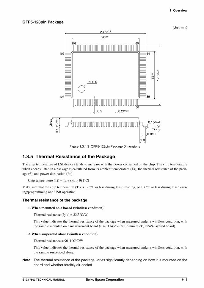
1 Overview
S1C17803 TECHNICAL MANUAL Seiko Epson Corporation 1-19
QFP5-128pin Package(Unit: mm)
20±0.1
23.6±0.4
65102
14±0
.1
17.6
±0.4
39
64
INDEX
0.2±0.05381
128
1032.
7±0.
10.
1
3max
1.8
0.8±0.2
0°10°
0.15±0.05
0.5
Figure 1.3.4.3 QFP5-128pin Package Dimensions
1.3.5 Thermal Resistance of the Package
The chip temperature of LSI devices tends to increase with the power consumed on the chip. The chip temperature when encapsulated in a package is calculated from its ambient temperature (Ta), the thermal resistance of the pack-age (θ), and power dissipation (PD).
Chip temperature (Tj) = Ta + (PD × θ) [°C]
Make sure that the chip temperature (Tj) is 125°C or less during Flash reading, or 100°C or less during Flash eras-ing/programming and USB operation.
Thermal resistance of the package
1. When mounted on a board (windless condition) Thermal resistance (θj-a) = 33.3°C/W
This value indicates the thermal resistance of the package when measured under a windless condition, with the sample mounted on a measurement board (size: 114 × 76 × 1.6 mm thick, FR4/4 layered board).
2. When suspended alone (windless condition)
Thermal resistance = 90–100°C/W
This value indicates the thermal resistance of the package when measured under a windless condition, with the sample suspended alone.
Note: The thermal resistance of the package varies significantly depending on how it is mounted on the board and whether forcibly air-cooled.
2 CPU
S1C17803 TECHNICAL MANUAL Seiko Epson Corporation 2-1
2 CPUThe S1C17803 contains the S1C17 Core as its core processor. The S1C17 Core is a Seiko Epson original 16-bit RISC-type processor.It features low power consumption, high-speed operation, large address space, main instructions executable in one clock cycle, and a small sized design. The S1C17 Core is suitable for embedded applications such as controllers and sequencers for which an eight-bit CPU is commonly used.For details of the S1C17 Core, refer to the “S1C17 Family S1C17 Core Manual.”
2.1 Features of the S1C17 Core
Processor type• Seiko Epson original 16-bit RISC processor
Instruction set• Code length: 16-bit fixed length• Number of instructions: 111 basic instructions (184 including variations)• Execution cycle: Main instructions executed in one cycle• Extended immediate instructions: Immediate extended up to 24 bits• Compact and fast instruction set optimized for development in C language
Register set• Eight 24-bit general-purpose registers• Two 24-bit special registers• One 8-bit special register
Memory space and bus• Up to 16M bytes of memory space (24-bit address)• Harvard architecture using separated instruction bus (16 bits) and data bus (32 bits)
Interrupts• Reset, NMI, and 32 external interrupts supported• Address misaligned interrupt• Debug interrupt• Direct branching from vector table to interrupt handler routine• Programmable software interrupts with a vector number specified (all vector numbers specifiable)
Power saving• HALT (halt instruction)• SLEEP (slp instruction)
Coprocessor interface• 16-bit × 16-bit multiplier• 16-bit ÷ 16-bit divider• 16-bit × 16-bit + 32-bit multiply and accumulation unit

2 CPU
2-2 Seiko Epson Corporation S1C17803 TECHNICAL MANUAL
2.2 CPU RegistersThe S1C17 Core contains eight general-purpose registers and three special registers.
R4R5R6R7
R3R2R1R0
bit 23 bit 0
General-purpose registers
PCbit 23
76543210
bit 0
PSRSP
Special registers
IL[2:0]7 6 5
IE4
C3
V2
Z1
N0
Figure 2.2.1 Registers
2.3 Instruction SetThe S1C17 Core instruction codes are all fixed to 16 bits in length which, combined with pipelined processing, al-lows most important instructions to be executed in one cycle. For details, refer to the “S1C17 Family S1C17 Core Manual.”
Table 2.3.1 List of S1C17 Core InstructionsClassification Mnemonic Function
Data transfer ld.b %rd,%rs General-purpose register (byte) → general-purpose register (sign-extended)%rd,[%rb] Memory (byte) → general-purpose register (sign-extended)
Memory address post-increment, post-decrement, and pre-decrement functions can be used.
%rd,[%rb]+
%rd,[%rb]-
%rd,-[%rb]
%rd,[%sp+imm7] Stack (byte) → general-purpose register (sign-extended)%rd,[imm7] Memory (byte) → general-purpose register (sign-extended)[%rb],%rs General-purpose register (byte) → memory
Memory address post-increment, post-decrement, and pre-decrement functions can be used.
[%rb]+,%rs
[%rb]-,%rs
-[%rb],%rs
[%sp+imm7],%rs General-purpose register (byte) → stack [imm7],%rs General-purpose register (byte) → memory
ld.ub %rd,%rs General-purpose register (byte) → general-purpose register (zero-extended)%rd,[%rb] Memory (byte) → general-purpose register (zero-extended)
Memory address post-increment, post-decrement, and pre-decrement functions can be used.
%rd,[%rb]+
%rd,[%rb]-
%rd,-[%rb]
%rd,[%sp+imm7] Stack (byte) → general-purpose register (zero-extended)%rd,[imm7] Memory (byte) → general-purpose register (zero-extended)
ld %rd,%rs General-purpose register (16 bits) → general-purpose register%rd,sign7 Immediate → general-purpose register (sign-extended)%rd,[%rb] Memory (16 bits) → general-purpose register
Memory address post-increment, post-decrement, and pre-decrement functions can be used.
%rd,[%rb]+
%rd,[%rb]-
%rd,-[%rb]
%rd,[%sp+imm7] Stack (16 bits) → general-purpose register%rd,[imm7] Memory (16 bits) → general-purpose register[%rb],%rs General-purpose register (16 bits) → memory
Memory address post-increment, post-decrement, and pre-decrement functions can be used.
[%rb]+,%rs
[%rb]-,%rs
-[%rb],%rs
[%sp+imm7],%rs General-purpose register (16 bits) → stack [imm7],%rs General-purpose register (16 bits) → memory
ld.a %rd,%rs General-purpose register (24 bits) → general-purpose register%rd,imm7 Immediate → general-purpose register (zero-extended)

2 CPU
S1C17803 TECHNICAL MANUAL Seiko Epson Corporation 2-3
Classification Mnemonic FunctionData transfer ld.a %rd,[%rb] Memory (32 bits) → general-purpose register (*1)
Memory address post-increment, post-decrement, and pre-decrement functions can be used.
%rd,[%rb]+
%rd,[%rb]-
%rd,-[%rb]
%rd,[%sp+imm7] Stack (32 bits) → general-purpose register (*1)%rd,[imm7] Memory (32 bits) → general-purpose register (*1)[%rb],%rs General-purpose register (32 bits, zero-extended) → memory (*1)
Memory address post-increment, post-decrement, and pre-decrement functions can be used.
[%rb]+,%rs
[%rb]-,%rs
-[%rb],%rs
[%sp+imm7],%rs General-purpose register (32 bits, zero-extended) → stack (*1)[imm7],%rs General-purpose register (32 bits, zero-extended) → memory (*1)%rd,%sp SP → general-purpose register%rd,%pc PC → general-purpose register%rd,[%sp] Stack (32 bits) → general-purpose register (*1)
Stack pointer post-increment, post-decrement, and pre-decrement functions can be used.
%rd,[%sp]+
%rd,[%sp]-
%rd,-[%sp]
[%sp],%rs General-purpose register (32 bits, zero-extended) → stack (*1)Stack pointer post-increment, post-decrement, and pre-decrement functions can be used.
[%sp]+,%rs
[%sp]-,%rs
-[%sp],%rs
%sp,%rs General-purpose register (24 bits) → SP %sp,imm7 Immediate → SP
Integer arithmetic operation
add %rd,%rs 16-bit addition between general-purpose registersSupports conditional execution (/c: executed if C = 1, /nc: executed if C = 0).add/c
add/nc
add %rd,imm7 16-bit addition of general-purpose register and immediateadd.a %rd,%rs 24-bit addition between general-purpose registers
Supports conditional execution (/c: executed if C = 1, /nc: executed if C = 0).add.a/c
add.a/nc
add.a %sp,%rs 24-bit addition of SP and general-purpose register%rd,imm7 24-bit addition of general-purpose register and immediate%sp,imm7 24-bit addition of SP and immediate
adc %rd,%rs 16-bit addition with carry between general-purpose registersSupports conditional execution (/c: executed if C = 1, /nc: executed if C = 0).adc/c
adc/nc
adc %rd,imm7 16-bit addition of general-purpose register and immediate with carry sub %rd,%rs 16-bit subtraction between general-purpose registers
Supports conditional execution (/c: executed if C = 1, /nc: executed if C = 0).sub/c
sub/nc
sub %rd,imm7 16-bit subtraction of general-purpose register and immediatesub.a %rd,%rs 24-bit subtraction between general-purpose registers
Supports conditional execution (/c: executed if C = 1, /nc: executed if C = 0).sub.a/c
sub.a/nc
sub.a %sp,%rs 24-bit subtraction of SP and general-purpose register%rd,imm7 24-bit subtraction of general-purpose register and immediate%sp,imm7 24-bit subtraction of SP and immediate
sbc %rd,%rs 16-bit subtraction with carry between general-purpose registersSupports conditional execution (/c: executed if C = 1, /nc: executed if C = 0).sbc/c
sbc/nc
sbc %rd,imm7 16-bit subtraction of general-purpose register and immediate with carry cmp %rd,%rs 16-bit comparison between general-purpose registers
Supports conditional execution (/c: executed if C = 1, /nc: executed if C = 0).cmp/c
cmp/nc
cmp %rd,sign7 16-bit comparison of general-purpose register and immediatecmp.a %rd,%rs 24-bit comparison between general-purpose registers
Supports conditional execution (/c: executed if C = 1, /nc: executed if C = 0).cmp.a/c
cmp.a/nc
cmp.a %rd,imm7 24-bit comparison of general-purpose register and immediate cmc %rd,%rs 16-bit comparison with carry between general-purpose registers
Supports conditional execution (/c: executed if C = 1, /nc: executed if C = 0).cmc/c
cmc/nc
cmc %rd,sign7 16-bit comparison of general-purpose register and immediate with carry

2 CPU
2-4 Seiko Epson Corporation S1C17803 TECHNICAL MANUAL
Classification Mnemonic FunctionLogical operation and %rd,%rs Logical AND between general-purpose registers
Supports conditional execution (/c: executed if C = 1, /nc: executed if C = 0).and/c
and/nc
and %rd,sign7 Logical AND of general-purpose register and immediateor %rd,%rs Logical OR between general-purpose registers
Supports conditional execution (/c: executed if C = 1, /nc: executed if C = 0).or/c
or/nc
or %rd,sign7 Logical OR of general-purpose register and immediatexor %rd,%rs Exclusive OR between general-purpose registers
Supports conditional execution (/c: executed if C = 1, /nc: executed if C = 0).xor/c
xor/nc
xor %rd,sign7 Exclusive OR of general-purpose register and immediatenot %rd,%rs Logical inversion between general-purpose registers (1's complement)
Supports conditional execution (/c: executed if C = 1, /nc: executed if C = 0).not/c
not/nc
not %rd,sign7 Logical inversion of general-purpose register and immediate (1's complement)Shift and swap sr %rd,%rs Logical shift to the right with the number of bits specified by the register
%rd,imm7 Logical shift to the right with the number of bits specified by immediatesa %rd,%rs Arithmetic shift to the right with the number of bits specified by the register
%rd,imm7 Arithmetic shift to the right with the number of bits specified by immediatesl %rd,%rs Logical shift to the left with the number of bits specified by the register
%rd,imm7 Logical shift to the left with the number of bits specified by immediateswap %rd,%rs Bytewise swap on byte boundary in 16 bits
Immediate extension ext imm13 Extend operand in the following instructionConversion cv.ab %rd,%rs Converts signed 8-bit data into 24 bits
cv.as %rd,%rs Converts signed 16-bit data into 24 bits cv.al %rd,%rs Converts 32-bit data into 24 bitscv.la %rd,%rs Converts 24-bit data into 32 bitscv.ls %rd,%rs Converts 16-bit data into 32 bits
Branch jpr
jpr.d
sign10 PC relative jumpDelayed branching possible%rb
jpa
ipa.d
imm7 Absolute jumpDelayed branching possible%rb
jrgt
jrgt.d
sign7 PC relative conditional jump Branch condition: !Z & !(N ^ V)Delayed branching possible
jrge
jrge.d
sign7 PC relative conditional jump Branch condition: !(N ^ V)Delayed branching possible
jrlt
jrlt.d
sign7 PC relative conditional jump Branch condition: N ^ VDelayed branching possible
jrle
jrle.d
sign7 PC relative conditional jump Branch condition: Z | N ^ VDelayed branching possible
jrugt
jrugt.d
sign7 PC relative conditional jump Branch condition: !Z & !CDelayed branching possible
jruge
jruge.d
sign7 PC relative conditional jump Branch condition: !CDelayed branching possible
jrult
jrult.d
sign7 PC relative conditional jump Branch condition: CDelayed branching possible
jrule
jrule.d
sign7 PC relative conditional jump Branch condition: Z | CDelayed branching possible
jreq
jreq.d
sign7 PC relative conditional jump Branch condition: ZDelayed branching possible
jrne
jrne.d
sign7 PC relative conditional jump Branch condition: !ZDelayed branching possible
call
call.d
sign10 PC relative subroutine callDelayed call possible%rb
calla
calla.d
imm7 Absolute subroutine callDelayed call possible%rb
ret
ret.d
Return from subroutineDelayed return possible
int imm5 Software interruptintl imm5,imm3 Software interrupt with interrupt level settingreti
reti.d
Return from interrupt handlingDelayed call possible
brk Debug interrupt

2 CPU
S1C17803 TECHNICAL MANUAL Seiko Epson Corporation 2-5
Classification Mnemonic FunctionBranch retd Return from debug processingSystem control nop No operation
halt HALT modeslp SLEEP modeei Enable interruptsdi Disable interrupts
Coprocessor control ld.cw %rd,%rs Transfer data to coprocessor%rd,imm7
ld.ca %rd,%rs Transfer data to coprocessor and get results and flag statuses%rd,imm7
ld.cf %rd,%rs Transfer data to coprocessor and get flag statuses%rd,imm7
*1 The ld.a instruction accesses memories in 32-bit length. During data transfer from a register to a memory, the 32-bit data in which the eight high-order bits are set to 0 is written to the memory. During reading from a memory, the eight high-order bits of the read data are ignored.
The symbols in the above table each have the meanings specified below.
Table 2.3.2 Symbol MeaningsSymbol Description
%rs General-purpose register, source%rd General-purpose register, destination[%rb] Memory addressed by general-purpose register[%rb]+ Memory addressed by general-purpose register with address post-incremented[%rb]- Memory addressed by general-purpose register with address post-decremented-[%rb] Memory addressed by general-purpose register with address pre-decremented%sp Stack pointer[%sp],[%sp+imm7] Stack[%sp]+ Stack with address post-incremented[%sp]- Stack with address post-decremented-[%sp] Stack with address pre-decrementedimm3,imm5,imm7,imm13 Unsigned immediate (numerals indicating bit length)sign7,sign10 Signed immediate (numerals indicating bit length)
2.4 Reading PSRThe S1C17803 incorporates the MISC_PSR register for reading the contents of the PSR (Processor Status Register) in the S1C17 Core. Reading the contents of this register makes it possible to check the contents of the PSR using the application software. Note that data cannot be written to the PSR.
PSR Register (MISC_PSR)Register name Address Bit Name Function Setting Init. R/W Remarks
PSR Register(MISC_PSR)
0x532c(16 bits)
D15–8 – reserved – – – 0 when being read.D7–5 PSRIL[2:0] PSR interrupt level (IL) bits 0x0 to 0x7 0x0 R
D4 PSRIE PSR interrupt enable (IE) bit 1 1 (enable) 0 0 (disable) 0 RD3 PSRC PSR carry (C) flag 1 1 (set) 0 0 (cleared) 0 RD2 PSRV PSR overflow (V) flag 1 1 (set) 0 0 (cleared) 0 RD1 PSRZ PSR zero (Z) flag 1 1 (set) 0 0 (cleared) 0 RD0 PSRN PSR negative (N) flag 1 1 (set) 0 0 (cleared) 0 R
D[15:8] Reserved
D[7:5] PSRIL[2:0]: PSR Interrupt Level (IL) Bits The value of the PSR IL (interrupt level) bits can be read out. (Default: 0x0)
D4 PSRIE: PSR Interrupt Enable (IE) Bit The value of the PSR IE (interrupt enable) bit can be read out. 1 (R): 1 (interrupt enabled) 0 (R): 0 (interrupt disabled) (default)

2 CPU
2-6 Seiko Epson Corporation S1C17803 TECHNICAL MANUAL
D3 PSRC: PSR Carry (C) Flag Bit The value of the PSR C (carry) flag can be read out. 1 (R): 1 0 (R): 0 (default)
D2 PSRV: PSR Overflow (V) Flag Bit The value of the PSR V (overflow) flag can be read out. 1 (R): 1 0 (R): 0 (default)
D1 PSRZ: PSR Zero (Z) Flag Bit The value of the PSR Z (zero) flag can be read out. 1 (R): 1 0 (R): 0 (default)
D0 PSRN: PSR Negative (N) Flag Bit The value of the PSR N (negative) flag can be read out. 1 (R): 1 0 (R): 0 (default)
2.5 Processor InformationThe S1C17803 has the IDIR register shown below that allows the application software to identify CPU core type.
Processor ID Register (IDIR)Register name Address Bit Name Function Setting Init. R/W Remarks
Processor ID Register(IDIR)
0xffff84(8 bits)
D7–0 IDIR[7:0] Processor ID0x10: S1C17 Core
0x10 0x10 R
This is a read-only register that contains the ID code to represent a processor model. The S1C17 Core’s ID code is 0x10.

3 Memory Map and Bus
S1C17803 TECHNICAL MANUAL Seiko Epson Corporation 3-1
3 Memory Map and BusFigure 3.1 shows the S1C17803 memory map.
Flash area(128K bytes)
(Device size: 16 bits)
Vector table
Internal peripheral area 2(4K bytes)
Internal peripheral area 3(12K bytes)
Internal peripheral area 1(1K bytes)
SRAMC #CE0 area(2M bytes)
(Device size: 8/16 bits)
SRAMC #CE1 area(4M bytes)
(Device size: 8/16 bits)
SRAMC #CE2 area(8M bytes)
(Device size: 8/16 bits)
SRAMC #CE3 area(1M bytes)
(Device size: 8/16 bits)
Reserved for core I/O area(1K bytes)
reserved
reserved
reserved
reserved
reserved
reserved
0xff ffff
0xff fc000xff fbff
0xff 00000xfe ffff
0xf0 00000xef ffff
0x70 00000x6f ffff
0x30 00000x2f ffff
0x10 00000x0f ffff
0x0c 40000x0c 3fff0x0c 3fc00x0c 3fbf
0x0c 00000x0b ffff
0x08 30000x08 2fff
0x08 00000x07 ffff
0x02 80000x02 7fff
0x00 80000x00 7fff
0x00 60000x00 5fff
0x00 50000x00 4fff
0x00 44000x00 43ff
0x00 40000x00 3fff
0x00 0000
0x4380–0x43ff0x4360–0x437f0x4340–0x435f0x4320–0x433f0x42e0–0x431f0x4270–0x42df0x4260–0x426f0x4220–0x425f0x4200–0x421f0x4120–0x41ff0x4100–0x411f0x4040–0x40ff0x4020–0x403f0x4000–0x401f
reservedI2C slaveI2C masterreservedInterrupt controllerreservedCLG_T8I timerreservedCLG_T16FU0 timerreservedUART w/IrDAreservedPrescalerreserved
0x5340–0x5fff0x5320–0x533f0x5000–0x531f
reservedMISC registersreserved
–(16 bits)–
–(16 bits)(16 bits)–(16 bits)–(16 bits)–(16 bits)–(8 bits)–(8 bits)–
Peripheral function (Device size)0x81b00–0x82fff0x81a00–0x81aff0x81900–0x819ff0x81800–0x818ff0x81700–0x817ff0x81600–0x816ff0x81500–0x815ff0x81400–0x814ff0x81300–0x813ff0x81200–0x812ff0x81100–0x811ff0x81000–0x810ff0x80910–0x80fff0x80900–0x8090f0x80800–0x808ff0x80700–0x807ff0x80500–0x806ff0x80400–0x804ff0x80300–0x803ff0x80200–0x802ff0x80100–0x801ff0x80000–0x800ff
reserved8-bit programmable timerLCD controllerDMA ControllerFlash controllerSRAM controllerI2S16-bit audio PWM timer16-bit PWM timerRemote controllerA/D converterWatchdog timerreservedBBRAMRealtime clockCard interfaceUniversal serial interfacereservedPrescalerPort MUXGPIOClock management unit
(16 bits)(16 bits)(16 bits)(16 bits)(16 bits)(16 bits)(16 bits)(16 bits)(16 bits)(16 bits)(16 bits)(16 bits)–(8 bits)(8 bits)(8 bits)(8 bits)–(8 bits)(8 bits)(8 bits)(8 bits)
IRAM/IVRAM mirror area
Debug RAM area (64 bytes)IRAM/IVRAM area
(16K bytes)(Device size: 16 bits)
Figure 3.1 S1C17803 Memory Map

3 Memory Map and Bus
3-2 Seiko Epson Corporation S1C17803 TECHNICAL MANUAL
3.1 Flash AreaThe S1C17803 contains a Flash memory (4K bytes/sector) in the 128K-byte area from address 0x8000 to address 0x27fff for storing application programs and data. Address 0x8000 is defined as the vector table base address by default, therefore the reset vector must be placed on this address. The vector table base address can be modified with the MISC_TTBRL/MISC_TTBRH registers.The Flash memory can be read in a minimum of one cycle.For more information on the Flash memory, see the “Flash Controller (FLASHC)” chapter.
3.2 IRAM/IVRAM AreaThe S1C17803 contains a RAM in the 16K-byte area from address 0xc0000 to address 0xc3fff. Addresses 0xc4000 to 0xfffff are a mirror area for the RAM. The RAM can be used as a general-purpose memory (IRAM) or a VRAM for the on-chip LCD controller (IVRAM).The IRAM/IVRAM is accessed in one cycle (min.) for data writing or two cycles (min.) for data reading.
Notes: • The 64-byte area at the end of the RAM (0xfffc0–0xfffff = 0xc3fc0–0xc3fff) is reserved for the on-chip debugger. When using the debug functions under application development, do not ac-cess this area from the application program.
This area can be used for applications of mass-produced devices that do not need debugging.
• When data is written to IRAM/IVRAM using the “ld.a” instruction, the S1C17 Core does not write anything to the eight high-order bits (D[31:24]) of the 32-bit space.
Example: ld.a [%rb],%rs
[%rb] 0b******00 Byte 0
7
78
0
Not written
16 15
Byte 0Byte 123
Byte 20
0b******01 Byte 10b******10 Byte 20b******11 Unchanged
%rs
Figure 3.2.1 24-bit Write to IRAM/IVRAM
3.3 BBRAM AreaThe S1C17803 contains a 16-byte RAM (BBRAM) from address 0x80900 to address 0x8090f. This RAM uses RTCVDD as its operating voltage. This makes it possible to use BBRAM as a battery backup RAM that maintains the contents even if the system power is shut down.The BBRAM is accessed in three cycles (min.).
3.4 Internal Peripheral AreaThe I/O and control registers for the internal peripheral modules are located in the 1K-byte area beginning with ad-dress 0x4000, 4K-byte area beginning with address 0x5000, and 12K-byte area beginning with address 0x80000.For details of each control register, see the I/O register list in Appendix or descriptions for each peripheral module.
Internal Peripheral Area 1 (0x4000–0x43ff) The internal peripheral area 1 beginning with address 0x4000 contains the I/O memory for the peripheral func-
tions listed below and this area can be accessed in one cycle.• Prescaler (PSC Ch.0, 8-bit device)• UART (UART, 8-bit device)• Clock generator (CLG, 16-bit device)• Interrupt controller (ITC, 16-bit device)• I2C master (I2CM, 16-bit device)• I2C slave (I2CS, 16-bit device)

3 Memory Map and Bus
S1C17803 TECHNICAL MANUAL Seiko Epson Corporation 3-3
Internal Peripheral Area 2 (0x5000–0x5fff) The internal peripheral area 2 beginning with address 0x5000 contains the I/O memory for the peripheral func-
tion listed below and this area can be accessed in one cycle.• MISC registers (MISC, 16-bit device)
Internal Peripheral Area 3 (0x80000–0x82fff) The internal peripheral area 3 beginning with address 0x80000 contains the I/O memory for the peripheral
function listed below and this area can be accessed in three cycles (min.).• Clock management unit (CMU, 8-bit device)• GPIO & port MUX (GPIO, 8-bit device)• Prescaler (PSC Ch.1 & 2, 8-bit device)• Universal serial interface (USI, 8-bit device)• Card interface (CARD, 8-bit device)• Real-time clock (RTC, 8-bit device)• BBRAM (BBRAM, 8-bit device)• Watchdog timer (WDT, 16-bit device)• A/D converter (ADC10, 16-bit device)• Remote controller (REMC, 16-bit device)• 16-bit PWM timer (T16A, 16-bit device)• 16-bit audio PWM timer (T16P, 16-bit device)• I2S (I2S, 16-bit device)• SRAM controller (SRAMC, 16-bit device)• Flash controller (FLASHC, 16-bit device)• DMA controller (DMAC, 16-bit device)• LCD controller (LCDC, 16-bit device)• 8-bit programmable timer (T8F, 16-bit device)
3.5 S1C17 Core I/O AreaThe 1K-byte area from address 0xfffc00 to address 0xffffff is the I/O area for the CPU core in which the I/O regis-ters listed in the table below are located.
Table 3.5.1 S1C17 Core I/O AreaPeripheral Address Register name Function
S1C17 Core I/O 0xffff84 IDIR Processor ID Register Indicates the processor ID.0xffff90 DBRAM Debug RAM Base Register Indicates the debug RAM base address.0xffffa0 DCR Debug Control Register Debug control0xffffb4 IBAR1 Instruction Break Address Register 1 Instruction break address #1 setting0xffffb8 IBAR2 Instruction Break Address Register 2 Instruction break address #2 setting0xffffbc IBAR3 Instruction Break Address Register 3 Instruction break address #3 setting0xffffd0 IBAR4 Instruction Break Address Register 4 Instruction break address #4 setting
See “Processor Information” in the “CPU” chapter for more information on IDIR. See the “On-chip Debugger (DBG)” chapter for more information on other registers.This area incorporates the S1C17 Core registers, in addition to those described above. For more information on these registers, refer to the “S1C17 Core Manual.”

3 Memory Map and Bus
3-4 Seiko Epson Corporation S1C17803 TECHNICAL MANUAL
3.6 Internal BusFigure 3.6.1 shows the S1C17803 bus configuration.The S1C17803 incorporates a bus matrix that arbitrates accessing by the bus masters (S1C17 Core, DMA control-ler, and LCD controller). The bus matrix allows the bus masters to access a different bus slave at the same time. For example, while the LCDC is accessing the IVRAM via the IVRAM interface, the S1C17 Core can access an exter-nal memory via the SRAMC or an extended peripheral module via the SAPB bridge if it is not being accessed by the DMAC. If two or more bus masters access a same bus slave, the bus master with the highest priority is granted access. Other bus masters must wait until the higher priority bus master has finished accessing. Priority of bus masters: 1. LCDC → 2. DMAC → 3. S1C17 Core
Bus masters
Flash EEPROM
IRAM/IVRAM
S1C17 Core DMAC LCDC
MUL/MAC/DIV (DSP)
FLASHC
Bus matrix
Core peripheral modules(0x4000–0x5fff)
External memoryExtended peripheral
modules (0x80000–0x82fff)
Bus slaves
SRAMCIVRAM
interfaceSAPBBridge
Figure 3.6.1 Bus Configuration
3.7 Access CycleAs shown in Table 3.7.1, the number of cycles required for one bus access depends on the peripheral or memory module. Furthermore, the number of bus accesses depends on the CPU instruction (access size) and device size.
Table 3.7.1 Number of Access Cycles for Data Read/WriteModule Access condition Write Read
Embedded FLASH
CPU access 8-bit access – 1 + w16-bit access Software control 1 + w24/32-bit access – (1 + w) × 2
IRAM/IVRAM CPU/DMA access 8-bit access 1 + w 2 + w16-bit access 1 + w 2 + w24/32-bit access 2 3
LCDC access 16-bit access – 2Peripheral module registers
8-bit deviceCPU/DMA access
8-bit access 3 + w 3 + w16-bit access (3 + w) × 2 (3 + w) × 224/32-bit access (3 + w) × 4 (3 + w) × 4
16-bit deviceCPU/DMA access
8-bit access 3 + w 3 + w16-bit access 3 + w 3 + w24-bit access (3 + w) × 2 (3 + w) × 2

3 Memory Map and Bus
S1C17803 TECHNICAL MANUAL Seiko Epson Corporation 3-5
Module Access condition Write Read
External memory 8-bit RAMCPU/DMA access
8-bit access 3 + w 3 + w16-bit access (3 + w) × 2 (3 + w) × 224/32-bit access (3 + w) × 4 (3 + w) × 4
8-bit RAMCPU/DMA burst read
8-bit × N access – 3 + (1 + w) × N16-bit × N access – 3 + (1 + w) × 2N24/32-bit × N access – 3 + (1 + w) × 4N
16-bit RAMCPU/DMA access
8-bit access 3 + w 3 + w16-bit access 3 + w 3 + w24/32-bit access (3 + w) × 2 (3 + w) × 2
16-bit RAMCPU/DMA burst read
8-bit × N access – 3 + (1 + w) × N16-bit × N access – 3 + (1 + w) × N24/32-bit × N access – 3 + (1 + w) × 2N
8-bit RAM LCDC read 16-bit access – 3 + w16-bit RAM LCDC read 16-bit access – 3 + w
Coprocessor MUL (16 bits × 16 bits) 1 + wMAC (16 bits × 16 bits + 32 bits) 1 + wDIV (16 bits ÷ 16 bits) 17 + w
Notes: • “w” means the number of wait cycles.
• “N” means the number of burst cycles.
• The LCDC does not support burst read.
Handling the eight high-order bits during 32-bit accesses During writing, the eight high-order bits of 32-bit data are written as 0. However, the eight high-order bits are
not written when data is written to IRAM/IVRAM using the “ld.a” instruction. During reading from a memory, the eight high-order bits are ignored. However, the eight high-order bits are ef-
fective as the PSR value only in the stack operation when an interrupt occurs.
Simultaneous Access to Instruction and Data by Harvard Architecture The S1C17 Core has adopted Harvard Architecture. An instruction fetch and a data access are performed simul-
taneously under one of the conditions listed below, this makes it possible to improve the execution speed.
• When the S1C17 Core executes the instruction stored in the Flash area and accesses data in the IRAM/IVRAM, an internal peripheral area, or an external memory
• When the S1C17 Core executes the instruction stored in the IRAM/IVRAM area or an external memory and accesses data in the Flash area

4 Power Supply
S1C17803 TECHNICAL MANUAL Seiko Epson Corporation 4-1
4 Power SupplyThis section explains the operating voltage of the S1C17803.
4.1 Power Supply PinsThe S1C17803 has the power supply pins shown in Table 4.1.1.
Table 4.1.1 Power Supply Pins
Pin namePin No.
I/O Voltage PU/PD DescriptionTQFP14-100pin
TQFP15-128pin
QFP5-128pin
BUSIO_VDD 1 1 100 – 2.7 to 5.5 V – Bus group I/O voltage power supply (+) IO1_VDD 47 59 30 – 2.7 to 5.5 V – Group 1 I/O voltage power supply (+)IO2_VDD 68 87 58 – 2.7 to 5.5 V – Group 2 I/O voltage power supply (+)LVDD 30 37 8 – 2.7 to 3.6 V – S1C17 Core voltage power supply (+)REGU_VDD 31 38 9 – 4.5 to 5.5 V – Regulator power supply (+)REGU_VSS 32 39 10 – GND – Regulator groundREGU_CE 29 36 7 I (Analog) – Regulator enable inputVSS 9, 16, 39,
46, 75, 85, 86, 92
13, 22, 47, 58, 95, 106, 107, 117
18, 29, 66, 77, 78, 88,
112, 121
– GND – Ground
RTCVDD 35 42 13 – 2.7 to 3.6 V – RTC/BBRAM power supply (+)(RTCVDD = LVDD)
AVDD 28 35 6 – 2.7 to 5.5 V – Analog power supply
I/O Group 1interface circuit
Bus interface circuit
LVDD
REGU_VDD
REGU_VSS
REGU_CE
3.0 or 3.3 V Typ.(2.7 to 3.6 V)
BUSIO_VDD
IO1_VDD
IO2_VDD
VSS
AVDD
BBRAM
3.3 Vregulator
I/O Group 2interface circuit
Analog circuits(A/D converter)
RTCVDD3.3 V Typ.(2.7 to 3.6 V)
CPU coreInternal logic
circuits
RTC/OSC1
(1) When 3.3 V single power source is used (internal regulator not used)
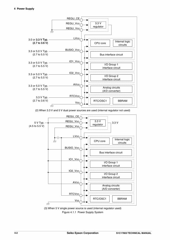
4 Power Supply
4-2 Seiko Epson Corporation S1C17803 TECHNICAL MANUAL
I/O Group 1interface circuit
Bus interface circuit
LVDD
REGU_VDD
REGU_VSS
REGU_CE
3.3 V Typ.(2.7 to 3.6 V)
3.0 or 3.3 V Typ.(2.7 to 3.6 V)
BUSIO_VDD
IO1_VDD
IO2_VDD
VSS
AVDD
BBRAM
3.3 Vregulator
I/O Group 2interface circuit
Analog circuits(A/D converter)
RTCVDD3.3 V Typ.(2.7 to 3.6 V)
3.3 or 5.0 V Typ.(2.7 to 5.5 V)
3.3 or 5.0 V Typ.(2.7 to 5.5 V)
3.3 or 5.0 V Typ.(2.7 to 5.5 V)
3.3 or 5.0 V Typ.(2.7 to 5.5 V)
CPU coreInternal logic
circuits
RTC/OSC1
(2) When 3.3 V and 5 V dual power sources are used (internal regulator not used)
I/O Group 1interface circuit
Bus interface circuit
CPU coreInternal logic
circuits
LVDD
REGU_VDD
REGU_VSS
REGU_CE
5 V Typ.(4.5 to 5.5 V)
BUSIO_VDD
IO1_VDD
IO2_VDD
VSS
AVDD
RTC/OSC1 BBRAM
3.3 Vregulator
I/O Group 2interface circuit
Analog circuits(A/D converter)
RTCVDD
3.3 V
(3) When 5 V single power source is used (internal regulator used)
Figure 4.1.1 Power Supply System
4 Power Supply
S1C17803 TECHNICAL MANUAL Seiko Epson Corporation 4-3
4.2 Operating Voltage (LVDD)The CPU core and internal logic circuits operate with a voltage supplied between the LVDD and VSS pins. The following operating voltage can be used:
LVDD = 2.7 V to 3.6 V (VSS = GND)
Note: When using a 5 V power supply for driving the CPU core and internal logic circuits, the internal operating voltage should be generated by the internal 3.3 V regulator.
4.3 I/O Interface Voltages (BUSIO_VDD, IO1_VDD, IO2_VDD)The I/O ports of the S1C17803 are divided into three groups and they can be driven with different power supply voltages. The following shows the power supply voltage and the pins belong to each I/O group.
Table 4.3.1 I/O Group and I/O Interface VoltagePower supply pin Supply voltage I/O group I/O pin (default function)
BUSIO_VDD 2.7 V to 5.5 V(VSS = GND)
BUS group P6[7:0], P7[7:0], P8[6:0], P9[7:0], PA[7:0], PB[7:0], TVEP
IO1_VDD 2.7 V to 5.5 V(VSS = GND)
I/O group 1 TEST, #RESET, #NMI, DCLK, DSIO, DST2, P1[7:0], P2[7:0], P3[5:0]
IO2_VDD 2.7 V to 5.5 V(VSS = GND)
I/O group 2 P4[5:0], P5[7:0], PC[7:0]
4.4 Power Supply for RTC (RTCVDD)The RTC power supply pin (RTCVDD) is provided separately from the LVDD pin in order to run the RTC and OSC1 oscillator at system power down. Supply the same voltage level as the LVDD to the RTCVDD pin.
RTCVDD = LVDD (2.7 V to 3.6 V, VSS = GND)
The RTCVDD is also used for the battery-backup RAM (BBRAM).
4.5 Power Supply for Analog Circuits (AVDD)The analog power supply pin (AVDD) is provided separately from other power supply pins in order that the digital circuits do not affect the analog circuit (A/D converter). The AVDD pin is used to supply an analog power voltage and the VSS pin is used as the analog ground. The following voltage is enabled for AVDD:
AVDD = 2.7 V to 5.5 V (VSS = GND)
Note: Be sure to supply a voltage within the range from 2.7 to 5.5 V to the AVDD pin even if the analog circuit is not used. It is not necessary to supply a voltage same as the LVDD level.
Noise on the analog power lines decrease the A/D converting precision, so use a stabilized power supply and make the board pattern with consideration given to that.
4.6 Internal Voltage RegulatorIn order to operate with a 5 V single power supply, the S1C17803 incorporates a voltage regulator that generates 3.3 V internal operating voltage. To use the internal voltage regulator, supply a 5 V power voltage to the REGU_VDD pin and set the REGU_CE pin to the REGU_VDD level. The regulator generates 3.3 V and supplies it to the inter-nal circuits instead of LVDD. Also the generated voltage is output from the LVDD pin and it can be supplied to the RTCVDD pin to operate the RTC.
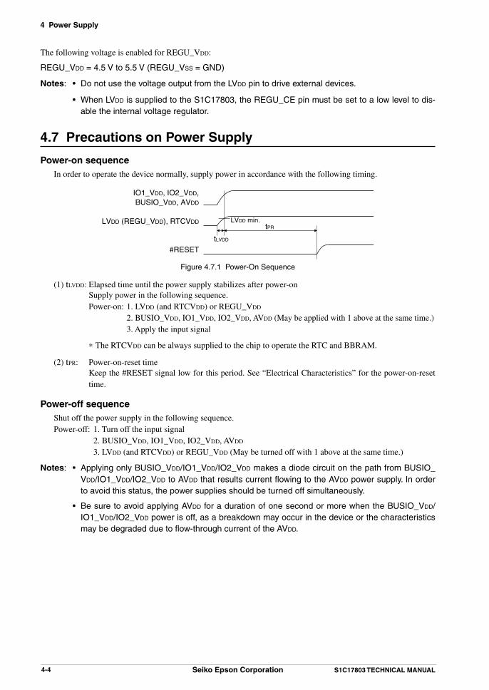
4 Power Supply
4-4 Seiko Epson Corporation S1C17803 TECHNICAL MANUAL
The following voltage is enabled for REGU_VDD:
REGU_VDD = 4.5 V to 5.5 V (REGU_VSS = GND)
Notes: • Do not use the voltage output from the LVDD pin to drive external devices.
• When LVDD is supplied to the S1C17803, the REGU_CE pin must be set to a low level to dis-able the internal voltage regulator.
4.7 Precautions on Power Supply
Power-on sequence In order to operate the device normally, supply power in accordance with the following timing.
IO1_VDD, IO2_VDD,BUSIO_VDD, AVDD
LVDD (REGU_VDD), RTCVDD
#RESET
LVDD min.
tLVDD
tPR
Figure 4.7.1 Power-On Sequence
(1) tLVDD: Elapsed time until the power supply stabilizes after power-on Supply power in the following sequence. Power-on: 1. LVDD (and RTCVDD) or REGU_VDD
2. BUSIO_VDD, IO1_VDD, IO2_VDD, AVDD (May be applied with 1 above at the same time.) 3. Apply the input signal
* The RTCVDD can be always supplied to the chip to operate the RTC and BBRAM.
(2) tPR: Power-on-reset time Keep the #RESET signal low for this period. See “Electrical Characteristics” for the power-on-reset
time.
Power-off sequence Shut off the power supply in the following sequence. Power-off: 1. Turn off the input signal 2. BUSIO_VDD, IO1_VDD, IO2_VDD, AVDD
3. LVDD (and RTCVDD) or REGU_VDD (May be turned off with 1 above at the same time.)
Notes: • Applying only BUSIO_VDD/IO1_VDD/IO2_VDD makes a diode circuit on the path from BUSIO_VDD/IO1_VDD/IO2_VDD to AVDD that results current flowing to the AVDD power supply. In order to avoid this status, the power supplies should be turned off simultaneously.
• Be sure to avoid applying AVDD for a duration of one second or more when the BUSIO_VDD/IO1_VDD/IO2_VDD power is off, as a breakdown may occur in the device or the characteristics may be degraded due to flow-through current of the AVDD.

4 Power Supply
S1C17803 TECHNICAL MANUAL Seiko Epson Corporation 4-5
Latch-up The CMOS device may be in the latch-up condition. This is the phenomenon caused by conduction of the para-
sitic PNPN junction (thyristor) contained in the CMOS IC, resulting in a large current between LVDD and VSS and leading to breakage.
Latch-up occurs when the voltage applied to the input/output exceeds the rated value and a large current flows into the internal element, or when the voltage at the LVDD pin exceeds the rated value and the internal element is in the breakdown condition. In the latter case, even if the application of a voltage exceeding the rated value is instantaneous, the current remains high between LVDD and VSS once the device is in the latch-up condition. As this may result in heat generation or smoking, the following points must be taken into consideration:(1) The voltage level at the input/output must not exceed the range specified in the electrical characteristics. In
other words, it must be below the power-supply voltage and above VSS. The power-on timing should also be taken into consideration.
(2) Abnormal noise must not be applied to the device.(3) The potential at the unused input should be fixed at LVDD, BUSIO_VDD, IO1_VDD, IO2_VDD, AVDD, or
VSS.(4) No outputs should be shorted.

5 Reset and NMI
S1C17803 TECHNICAL MANUAL Seiko Epson Corporation 5-1
5 Reset and NMI
5.1 Initial ResetThe S1C17803 has two initial reset sources that initialize the internal circuits.
(1) #RESET pin (external initial reset)(2) Watchdog timer (software selectable internal initial reset)
Figure 5.1.1 shows the configuration of the initial reset circuit.
#RESETReset input signal
Internal reset signalWDT reset signalWatchdog
timer
Wait timer
Figure 5.1.1 Configuration of Initial Reset Circuit
The CPU and peripheral circuits are initialized by the active signal from an initial reset source. When the reset sig-nal is negated, the CPU starts reset handling. The reset handling reads the reset vector (reset handler start address) from the beginning of the vector table and starts executing the program (initial routine) beginning with the read ad-dress.
5.1.1 #RESET Pin
By setting the #RESET pin to low level, the S1C17803 enters initial reset state. In order to initialize the S1C17803 for sure, the #RESET pin must be held at low for more than the prescribed time (see “AC Characteristics” in the “Electrical Characteristics” chapter) after the power supply voltage is supplied.Initial reset state is canceled when the #RESET pin at low level is set to high level.
5.1.2 Resetting by the Watchdog Timer
The S1C17803 has a built-in watchdog timer to detect runaway of the CPU. The watchdog timer outputs a signal if it is not reset with software (due to CPU runaway) in the programmed cycles. The output signal can generate either NMI or reset. Write 1 to the RESEN/WDT_EN register to generate reset.For details of the watchdog timer, see the “Watchdog Timer (WDT)” chapter.
Notes: • When using the reset function of the watchdog timer, program the watchdog timer so that it will be reset within the programmed cycles to avoid occurrence of an unnecessary reset.
• The reset function of the watchdog timer cannot be used for power-on reset as it must be en-abled with software.
5.1.3 Initial Reset Sequence
Even if the #RESET pin input negates the reset signal after power is turned on, the CPU cannot boot up until the oscillation stabilization waiting time (128 / OSC3 clock frequency) has elapsed. Figure 5.1.3.1 shows the operating sequence following cancellation of initial reset.The CPU starts operating in synchronization with the OSC3 clock after reset state is canceled.
Note: The oscillation stabilization time described in this section does not include oscillation start time. Therefore the time interval until the CPU starts executing instructions after power is turned on or SLEEP mode is canceled may be longer than that indicated in the figure below.

5 Reset and NMI
5-2 Seiko Epson Corporation S1C17803 TECHNICAL MANUAL
Boot vector
Oscillation stabilization waiting time
Booting
OSC3 clock
#RESET
Internal reset
Internal data request
Internal data address
Internal reset canceled
Reset canceled
Figure 5.1.3.1 Operation Sequence Following Cancellation of Initial Reset
5.1.4 Initial Reset Status
The S1C17 Core and internal peripheral circuits are initialized while the internal reset signal is kept 0. The follow-ing shows the internal reset status:
CPU PC: The reset vector at address 0x8000 is loaded to the PC. CPU PSR: All the PSR bits are reset to 0.Other CPU registers: All the registers are cleared to 0.TTBR: Initialized to 0x8000 CPU operating clock: The CPU operates with the OSC3 × 1/1 clock.Oscillator circuit: The OSC3 oscillator circuit is turned on. The OSC1 oscillator circuit is always on.Clock supply to peripheral modules: All clocks are enabled except for the LCDC.I/O pin status: Initialized (see the “Pin Functions” section in the “Overview” chapter.) Other peripheral modules: Initialized or undefined (see each I/O map.)
Note: The S1C17803 does not support a hot reset feature that maintains I/O pin status and the TTBR value.
5.1.5 Precautions to be Taken during Initial Reset
Core CPU When initially reset, all internal registers of the core CPU are cleared to 0. The Stack Pointer (SP) also becomes
0 when it is initialized upon reset. Note that normal operation of the program cannot be guaranteed if an inter-rupt occurs before the stack is set up, as the PC or PSR value may be saved to an indeterminate location. To prevent such a problem, set the SP before an interrupt occurs.
Internal RAM The content of internal RAM becomes undefined when initially reset. Internal RAM must be initialized as re-
quired.
OSC3 oscillator circuit When initially reset, the OSC3 oscillator circuit starts oscillating, and when the reset signal is negated, the CPU
starts operating with the OSC3 clock. To prevent erratic operation due to an unstable clock when the chip is reset at power-on or while the OSC3 oscillator circuit is idle, the reset signal should not be negated until after oscillation stabilizes.
OSC1 oscillator circuit When the chip is reset at power-on, the OSC1 oscillator circuit also starts oscillating. The OSC1 oscillator cir-
cuit requires a longer time for oscillation to stabilize than the OSC3 oscillator circuit. (See the electrical char-acteristics table.) To prevent erratic operation due to an instable clock, the OSC1 clock should not be used until after this stabilization time elapses.

5 Reset and NMI
S1C17803 TECHNICAL MANUAL Seiko Epson Corporation 5-3
Input/output ports and input/output pins Initial reset initializes the control and data registers of the input/output ports, therefore, be set up back again in
a program.
Other internal peripheral circuits The control and data registers of other peripheral circuits are initialized or undefined by initial reset. Therefore,
these registers should be set up as required in a program. For details on how peripheral circuits are initialized by initial reset, see each I/O map or circuit description.
5.2 NMI Input The S1C17803 has two NMI sources that generate NMI.
(1) #NMI pin (external input)(2) Watchdog timer (software selectable)
Figure 5.2.1 shows the configuration of the NMI circuit.
#NMINMI input signal
NMI request signalWDT NMI signalWatchdog
timer
Noise filter
On/Off
Figure 5.2.1 Configuration of NMI Circuit
The NMI signal, which is input from the #NMI pin or generated by the watchdog timer (WDT), generates a non-maskable interrupt to the S1C17 Core. This interrupt takes precedence over other interrupts and is unconditionally accepted by the S1C17 Core.For details about NMI exception handling by the S1C17 Core, refer to the “S1C17 Family S1C17 Core Manual.”
5.2.1 #NMI Pin
Setting the #NMI pin to low level generate a non-maskable interrupt to the S1C17 Core.
5.2.2 NMI by the Watchdog Timer
The S1C17803 has a built-in watchdog timer to detect runaway of the CPU. The watchdog timer outputs a signal if it is not reset with software (due to CPU runaway) in the programmed cycles. The output signal can generate either NMI or reset. Write 1 to the NMIEN/WDT_EN register to generate NMI.For details of the watchdog timer, see the “Watchdog Timer (WDT)” chapter.
5.2.3 NMI Input Noise Filter
Since accidental activation of NMI by noise in the S1C17 Core input signal will cause unintended NMI process-ing, the S1C17803 incorporates a noise filter. The filter removes noise from the NMI signals before they reach the S1C17 Core. You can select to use or bypass the noise filter.The NMI input noise filter removes noise when NMINFE/CMU_NFEN register = 1 or it is bypassed when NMIN-FE = 0.The noise filter operates using the OSC3 clock divided by 8. When activated, they filter out noise with pulses not exceeding three clock cycles. This means the pulse width must be at least 16 cycles of the OSC3 clock to input as a valid signal.For more information on the control bit, see the “Clock Management Unit (CMU)” chapter.
Note: The NMI input noise filter should normally be enabled.

6 Clock Management Unit (CMU)
S1C17803 TECHNICAL MANUAL Seiko Epson Corporation 6-1
6 Clock Management Unit (CMU)
6.1 CMU Module OverviewThe CMU module controls the internal oscillators and the system clock.The features of the CMU module are listed below.
• Generates the operating clocks with the built-in oscillators. - OSC3 oscillator circuit: 33 MHz (max.) crystal or ceramic oscillator circuit Supports an external clock input. - OSC1 oscillator circuit: 32.768 kHz (typ.) crystal oscillator circuit Supports an external clock input.
• Switches the system clock. The system clock source can be selected from OSC3, and OSC1 with software.
• Generates the system clock by dividing the source clock by 1 to 32.
• Controls the clock supply to the peripheral modules.
• Controls the clocks according to the standby mode (HALT, or SLEEP).
• Controls a clock output to external devices.
To reduce current consumption, control the clock in conjunction with processing and use standby mode. For more information on reducing current consumption, see “Power Saving” in the appendix chapter.Figure 6.1.1 shows the clock system and CMU module configuration.
OSC3control
OSC3oscillator(33 MHz)
OSC1oscillator(32.768 kHz)
Reset/NMI control
NMIRESET
CMU
WDT#NMI
#RESET
OSC3
OSC4 OSC3
OSC
CLKSRC
CCLKHALT
SLEEPWakeup
OSC1
Power down control
Gate
To S1C17 Core
CMU_CLK
OSC1
OSC2
RTC
WAKEUP#STBY
Divider(1/1–1/16)
Gate
Gate
S1C17 Core
PSC Ch.0, CLG, UART, I2CM, I2CS, ITC
LCDC
IRAM/IVRAM, Bus matrix, SAPB, SRAMC, FLASHC, DMAC,LCDC (bus I/F, reg.), CMU (reg.)
PSC Ch.2, T8F Ch.1&2, USI Ch.1, ADC, GPIO, PMUX, WDT, REMC, CARD, RTC, BBRAM
PSC Ch.1, T8F Ch.0, USI Ch.0, T16A, I2S, T16P
CMU_CLKSEL
PCLK2
LCLK
Gate PCLK1SYSCLK
Gate PCLK_SOC
Gate BCLK
Divider(1/1–1/32)
Figure 6.1.1 CMU Module Configuration
Note: The CMU control registers at addresses 0x80000–0x80007 are write-protected. Before the CMU control registers can be rewritten, write protection of these registers must be removed by writing data 0x96 to CMUP[7:0]/CMU_PROTECT register. Note that since unnecessary rewrites to the CMU control registers could lead to erratic system operation, CMUP[7:0] should be set to other than 0x96 unless the CMU control registers must be rewritten.

6 Clock Management Unit (CMU)
6-2 Seiko Epson Corporation S1C17803 TECHNICAL MANUAL
6.2 CMU PinsTable 6.2.1 lists the input/output pins for the CMU module.
Table 6.2.1 List of CMU PinsPin name I/O Qty Function
OSC1 I 1 OSC1 oscillator input pinConnect a crystal resonator (32.768 kHz), a feedback resistor, and a gate capaci-tor. Or input an external clock.
OSC2 O 1 OSC1 oscillator output pinConnect a crystal resonator (32.768 kHz), a feedback resistor, a drain resistor, and a drain capacitor.
OSC3 I 1 OSC3 oscillator input pinConnect a crystal or ceramic resonator (max. 33 MHz), a feedback resistor, and a gate capacitor. Or input an external clock.
OSC4 O 1 OSC3 oscillator output pinConnect a crystal or ceramic resonator (max. 33 MHz), a feedback resistor, a drain resistor, and a drain capacitor.
CMU_CLK O 1 CMU_CLK output pinOutputs the clock selected from OSC3, OSC1, CCLK, BCLK, PCLK_SOC, PCLK1, PCLK2, and LCLK.
The CMU output pin (CMU_CLK) is shared with an I/O port and are initially set as general purpose I/O port pin. The pin function must be switched using the port function select bit to use the general purpose I/O port pin as the CMU output pin.For detailed information on pin function switching, see the “I/O Ports (GPIO)” chapter.
6.3 Oscillators
6.3.1 OSC3 Oscillator Circuit
The OSC3 oscillator circuit generates the main clock for high-speed operation of the S1C17 Core and peripheral circuits.
Structure of the OSC3 oscillator circuit The OSC3 oscillator circuit accommodates a crystal/ceramic oscillator and external clock input. Figure 6.3.1.1 shows the structure of the OSC3 oscillator circuit.
Oscillation circuit control signalSLEEP control
Oscillation circuit control signalSLEEP control
VSS
OSC4
OSC3
CD3
CG3
X'tal3 orCeramic
OSC3 clock
OSC4
OSC3
Externalclock
N.C.
VSS
LVDD
OSC3 clock
(1) Crystal/ceramic oscillation circuit (2) External clock input
Rf
Rd
Figure 6.3.1.1 OSC3 Oscillator Circuit
For use as a crystal or ceramic oscillator circuit, connect a crystal (X’tal3) or ceramic resonator and a feedback resistor (Rf), two capacitors (CG3, CD3) and, if necessary, a drain resistor (Rd) to the OSC3 and OSC4 pins and VSS.
To use an external clock, leave the OSC4 pin open and input an LVDD-level clock (with a 50% duty cycle) to the OSC3 pin.
The range of oscillation frequencies is as follows: • Crystal oscillator: 1 MHz (min.) to 33 MHz (max.) • Ceramic oscillator: 1 MHz (min.) to 33 MHz (max.) • External clock input: 33 MHz (max.)
For details of oscillation characteristics and external clock input characteristics, see “Electrical Characteristics.”

6 Clock Management Unit (CMU)
S1C17803 TECHNICAL MANUAL Seiko Epson Corporation 6-3
OSC3 oscillation on/off The OSC3 oscillator circuit stops oscillating when OSC3EN/CMU_OSCCTL register is set to 0 and starts os-
cillating when set to 1. The OSC3 oscillator circuit stops oscillating even in SLEEP mode. After an initial reset, OSC3EN is set to 1 and the OSC3 oscillator circuit is activated.
Stabilization wait time at start of OSC3 oscillation The OSC3 oscillator circuit incorporates an oscillation stabilization wait timer to prevent malfunctions due to
unstable clock operations at the start of OSC3 oscillation—e.g., after an initial reset, when waking from SLEEP, or when the OSC3 oscillator is turned on with software. The OSC3 clock is not supplied to the system until the time set for this timer has elapsed. Use OSC3WT[3:0]/CMU_OSCCTL register to select one of 16 oscillation stabilization wait times.
Table 6.3.1.1 OSC3 Oscillation Stabilization Wait Time SettingsOSC3WT[3:0] Oscillation stabilization wait time
0xf 16 cycles0xe 32 cycles0xd 64 cycles0xc 128 cycles0xb 256 cycles0xa 512 cycles0x9 1,024 cycles0x8 2,048 cycles0x7 4,096 cycles0x6 8,192 cycles0x5 16,384 cycles0x4 32,768 cycles0x3 65,536 cycles0x2 131,072 cycles0x1 262,144 cycles0x0 524,288 cycles
(Default: 0xc)
This is set to 128 cycles (OSC3 clock) after an initial reset.
Note: Oscillation stability will vary, depending on the resonator and other external components. Carefully consider the OSC3 oscillation stabilization wait time before reducing the time. When switching the system clock to OSC3 immediately after the OSC3 oscillator circuit is turned on, set the OSC3 oscillation stabilization wait time as follows:
OSC3 oscillation stabilization wait time [cycle] ≥ OSC3 oscillation start time [second] (max.) × fOSC3 [Hz]
Example: When OSC3 oscillation start time (max.) = 10 ms and fOSC3 = 33 MHz OSC3 oscillation stabilization wait time ≥ 330,000 [cycles]
OSC3WT[3:0] should be set to 0x0 (OSC3 oscillation stabilization wait time = 524,288 cycles).
6.3.2 OSC1 Oscillator Circuit
The S1C17803 contains an oscillator circuit (OSC1) used to generate a 32.768 kHz (typ.) clock as the clock source for timekeeping operation of the RTC. The OSC1 clock can also be used as a power-saving operating clock for the core system or peripheral circuits.
Structure of the OSC1 oscillator circuit The OSC1 oscillator circuit accommodates a crystal oscillator and external clock input. As for the RTC,
RTCVDD is used to supply power to this circuit. Figure 6.3.2.1 shows the structure of the OSC1 oscillator circuit.

6 Clock Management Unit (CMU)
6-4 Seiko Epson Corporation S1C17803 TECHNICAL MANUAL
Low level
OSC1
OSC2
OSC1
Externalclock
N.C.
VSS
RTCVDDOSC1
(1) Crystal oscillation circuit
VSS
OSC2
OSC1
(3) When not used
(2) External clock input
VSS
OSC2
OSC1
CD1
CG1
X'tal1 Rf
Rd
Figure 6.3.2.1 OSC1 Oscillator Circuit
For use as a crystal oscillator circuit, connect a crystal resonator X’tal1 (32.768 kHz, typ.), feedback resistor (Rf), two capacitors (CG1, CD1), and, if necessary, a drain resistor (Rd) to the OSC1 and OSC2 pins and VSS, as shown in the figure above.
To use an external clock, leave the OSC2 pin open and input an RTCVDD level clock (whose duty cycle is 50%) to the OSC1 pin.
The oscillator frequency/input clock frequency is 32.768 kHz (typ.). Make sure the crystal resonator or external clock used in the RTC has this clock frequency. With any other clock frequencies, the RTC cannot be used for timekeeping purposes.
For details of oscillation characteristics and the input characteristics of external clock, see “Electrical Charac-teristics.”
When not using the OSC1 oscillator circuit, connect the OSC1 pin to VSS and leave the OSC2 pin open.
Oscillation control The OSC1 oscillator always operates without controlling using a register.
Note: A finite time (see “Electrical Characteristics”) is required until oscillation stabilizes after the OSC1 oscillator starts oscillating at power-on. To prevent system malfunction, do not use the oscillator-derived clock until this oscillation stabilization time elapses.
6.4 System Clock Settings
OSC3 clockOSC1 clock
System clock (SYSCLK)
CLKSRC SYSCLKDIV[2:0]
OSC Divider(1/1–1/32)
Figure 6.4.1 System Clock Control Circuit
6.4.1 System Clock Source Selection
Either the OSC3 clock or the OSC1 clock can be selected as the system clock source using CLKSRC/CMU_OSC-SRC register. When CLKSRC is set to 0 (default), OSC3 is selected as the system clock source; when CLKSRC is set to 1, OSC1 is selected.The following shows system clock switching procedures:
Switching the system clock to OSC1 from OSC31. Wait until the OSC1 oscillation is stabilized if the system clock is switched immediately after the RTCVDD
is turned on.2. Select the OSC1 clock as the system clock. (CLKSRC = 1)
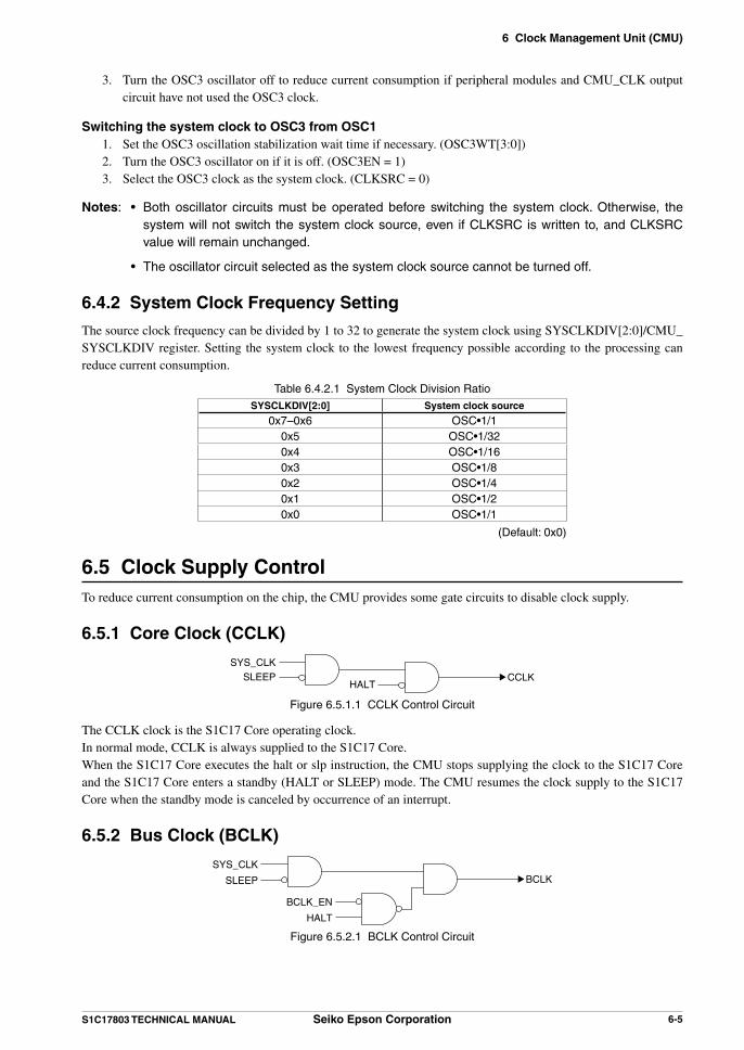
6 Clock Management Unit (CMU)
S1C17803 TECHNICAL MANUAL Seiko Epson Corporation 6-5
3. Turn the OSC3 oscillator off to reduce current consumption if peripheral modules and CMU_CLK output circuit have not used the OSC3 clock.
Switching the system clock to OSC3 from OSC11. Set the OSC3 oscillation stabilization wait time if necessary. (OSC3WT[3:0])2. Turn the OSC3 oscillator on if it is off. (OSC3EN = 1)3. Select the OSC3 clock as the system clock. (CLKSRC = 0)
Notes: • Both oscillator circuits must be operated before switching the system clock. Otherwise, the system will not switch the system clock source, even if CLKSRC is written to, and CLKSRC value will remain unchanged.
• The oscillator circuit selected as the system clock source cannot be turned off.
6.4.2 System Clock Frequency Setting
The source clock frequency can be divided by 1 to 32 to generate the system clock using SYSCLKDIV[2:0]/CMU_SYSCLKDIV register. Setting the system clock to the lowest frequency possible according to the processing can reduce current consumption.
Table 6.4.2.1 System Clock Division RatioSYSCLKDIV[2:0] System clock source
0x7–0x6 OSC•1/10x5 OSC•1/320x4 OSC•1/160x3 OSC•1/80x2 OSC•1/40x1 OSC•1/20x0 OSC•1/1
(Default: 0x0)
6.5 Clock Supply ControlTo reduce current consumption on the chip, the CMU provides some gate circuits to disable clock supply.
6.5.1 Core Clock (CCLK)
CCLKHALT
SYS_CLKSLEEP
Figure 6.5.1.1 CCLK Control Circuit
The CCLK clock is the S1C17 Core operating clock.In normal mode, CCLK is always supplied to the S1C17 Core.When the S1C17 Core executes the halt or slp instruction, the CMU stops supplying the clock to the S1C17 Core and the S1C17 Core enters a standby (HALT or SLEEP) mode. The CMU resumes the clock supply to the S1C17 Core when the standby mode is canceled by occurrence of an interrupt.
6.5.2 Bus Clock (BCLK)
BCLK
SYS_CLK
SLEEP
BCLK_EN
HALT
Figure 6.5.2.1 BCLK Control Circuit

6 Clock Management Unit (CMU)
6-6 Seiko Epson Corporation S1C17803 TECHNICAL MANUAL
The BCLK clock is used to operate the modules listed below.• IRAM/IVRAM• Bus matrix• SAPB bridge • SRAM controller (SRAMC)• Flash controller (FLASHC)• DMA controller (DMAC)• LCD controller (LCDC) bus interface and registers• Clock management unit (CMU) registers
BCLK is required for bus and memory operations, therefore, it is always supplied to the modules listed above in normal mode. However, the BCLK supply in HALT mode can be disabled using BCLK_EN/CMU_CLKCTL register if the LCDC and DMA do not need bus operations.To stop BCLK in HALT mode, set BCLK_EN to 0. The CMU stops supplying BCLK when the halt instruction is executed. The CMU resumes the clock supply when the HALT mode is canceled.To supply BCLK in HALT mode, set BCLK_EN to 1 (default). The modules listed above operates even in HALT mode.BCLK stops in SLEEP mode (when the slp instruction is executed) regardless of the BCLK_EN set value.
6.5.3 Peripheral Module Clocks (PCLK_SOC, PCLK1, PCLK2)
PCLK_SOCPCLKSOC_EN
SYS_CLKSLEEP
PCLK1PCLK1_EN
PCLK2PCLK2_EN
Figure 6.5.3.1 PCLK Control Circuit
The PCLK_SOC, PCLK1, and PCLK2 clocks are used to operate the modules listed below.
Table 6.5.3.1 Peripheral Modules and Operating ClocksClock Clock enable bit Peripheral modules
PCLK_SOC PCLKSOC_EN/CMU_CLKCTL register • Prescaler Ch.0 (PSC Ch.0)• Clock generator (CLG)• UART• I2C master (I2CM)• I2C slave (I2CS)• Interrupt controller (ITC)
PCLK1 PCLK1_EN/CMU_CLKCTL register • Prescaler Ch.1 (PSC Ch.1)• 8-bit programmable timer Ch.0 (T8F Ch.0)• 16-bit PWM timer (T16A)• 16-bit audio PWM timer (T16P)• Universal serial interface Ch.0 (USI Ch.0)• I2S (I2S)
PCLK2 PCLK2_EN/CMU_CLKCTL register • Prescaler Ch.2 (PSC Ch.2)• 8-bit programmable timer Ch.1, Ch.2 (T8F Ch.1, Ch.2)• Universal serial interface Ch.1 (USI Ch.1) • A/D converter (ADC10)• I/O ports and port MUX (GPIO)• Watchdog timer (WDT)• Remote controller (REMC)• Card interface (CARD)• Real-time clock (RTC) registers• BBRAM
The peripheral module clock (PCLK_SOC, PCLK1, PCLK2) supply can be controlled using the clock enable bit (PCLKSOC_EN, PCLK1_EN, PCLK2_EN).

6 Clock Management Unit (CMU)
S1C17803 TECHNICAL MANUAL Seiko Epson Corporation 6-7
The default setting of the clock enable bit is 1, which enables the clock supply. Disable the clock supply by setting the clock enable bit to 0 to reduce current consumption unless all the modules that use the clock need to be running.The clock is supplied even in HALT mode when the clock enable bit is set to 1. To stop the modules in HALT mode, set the clock enable bit to 0 before executing the halt instruction.In SLEEP mode (when the slp instruction is executed), these clocks stop even if the clock enable bit is set to 1.
6.5.4 LCDC Module Clock (LCLK)
LCLKLCLK_EN
OSC3
LCLKDIV[3:0]
Divider(1/1–1/16)
Figure 6.5.4.1 LCLK Control Circuit
The LCLK clock is generated by dividing the OSC3 clock and is supplied the LCD controller (LCDC). The fre-quency divider generates 16 kinds of clocks from OSC3•1/1 to OSC3•1/16. Select a divided clock according to the frame rate using LCLKDIV[3:0]/CMU_LCLK register.
fLCLK Frame rate = ————— [Hz] HT × VT
fLCLK: LCLK frequency HT: Horizontal total period (horizontal panel size + horizontal non-display period) [pixels] VT: Vertical total period (vertical panel size + vertical non-display period) [lines]
Table 6.5.4.1 LCDC Clock Division RatioLCLKDIV[3:0] LCLK
0xf OSC3•1/160xe OSC3•1/150xd OSC3•1/140xc OSC3•1/130xb OSC3•1/120xa OSC3•1/110x9 OSC3•1/100x8 OSC3•1/90x7 OSC3•1/80x6 OSC3•1/70x5 OSC3•1/60x4 OSC3•1/50x3 OSC3•1/40x2 OSC3•1/30x1 OSC3•1/20x0 OSC3•1/1
(Default: 0x7)
LCLK_EN/CMU_LCLK register is used for clock supply control (default: off). Before using the LCDC, set LCLK_EN to 1. Note that BCLK is required to set the LCDC registers.In HALT mode, LCLK does not stop if LCLK_EN is set to 1. To stop supplying the clock in HALT mode, LCLK_EN should be set to 0 before executing the halt instruction. In SLEEP mode (when the slp instruction is executed), LCLK stops even if LCLK_EN is set to 1.
Note: Disable LCLK supply (LCLK_EN = 0) when changing the clock division ratio using LCLKDIV[3:0] or before executing the slp instruction.

6 Clock Management Unit (CMU)
6-8 Seiko Epson Corporation S1C17803 TECHNICAL MANUAL
6.6 Clock External Output (CMU_CLK)An internally generated clock can be output from the CMU_CLK pin to external devices.CMU_CLK can be selected from among eight clocks using CMU_CLKSEL[3:0]/CMU_CMUCLK register.
Table 6.6.1 Selecting CMU_CLKCMU_CLKSEL[3:0] CMU_CLK
0xf–0x8 Reserved0x7 LCLK0x6 PCLK20x5 PCLK10x4 PCLK_SOC0x3 BCLK0x2 CCLK0x1 OSC10x0 OSC3
(Default: 0x0)
CMU_CLK can be selected at any time. However, switching over the clocks creates hazards.
Note: Settings other than those listed in Table 6.6.1 are reserved for testing. Do not set undescribed val-ues to CMU_CLKSEL[3:0] as undesired clocks may output.
6.7 Standby ModesThe S1C17803 supports two standby modes: HALT and SLEEP. Power consumption on the chip can be greatly re-duced by placing the CPU in one of these standby modes.
6.7.1 HALT Mode
The CPU suspends program execution upon executing the halt instruction and enters HALT mode. HALT mode is effective in reducing power consumption on the chip when running the CPU is unnecessary, such as when waiting for external input or responses from peripheral circuits. In HALT mode, the CPU stops operating. Furthermore, BCLK can be stopped in HALT mode (after the halt in-struction is executed) by setting BCLK_EN/CMU_CLKCTL register to 0 (see Sections 6.5.2 for BCLK). The other internal peripheral circuits remain in the state (idle or operating) held when the halt instruction was executed. The CPU is released from HALT mode by initial reset, an NMI or other interrupt, or a forcible break from the de-bugger. When an interrupt is used to cancel HALT mode, the S1C17 Core uses the interrupt signal sent from the interrupt controller (ITC). Therefore, the interrupts used to cancel HALT mode must be enabled in the interrupt source mod-ules. The S1C17 Core can restart from HALT mode even if the PSR is set to disable interrupts. When the IE (interrupt enable) bit in the PSR is set to 1 (enabled), the S1C17 Core executes the interrupt handler routine after HALT mode is canceled. When the IE bit is set to 0 (disabled), an interrupt does not occur and the S1C17 Core resumes execu-tion from the instruction that follows the halt instruction.The #NMI signal releases the CPU from HALT mode when it goes low level.
6.7.2 SLEEP Mode
The CPU suspends program execution upon executing the slp instruction and enters SLEEP mode. In SLEEP mode, the CPU stops operating and the CMU stops supplying clocks. Therefore, all peripheral modules (except for the OSC1 oscillator circuit and RTC) stop operating. The CPU is reawaken from SLEEP mode by initial reset, an RTC interrupt, an NMI, or other interrupt from an ex-ternal device (port input interrupt).

6 Clock Management Unit (CMU)
S1C17803 TECHNICAL MANUAL Seiko Epson Corporation 6-9
The S1C17 Core can restart from SLEEP mode even if the PSR is set to disable interrupts. When the IE (interrupt enable) bit in the PSR is set to 0 (disabled), an interrupt does not occur and the S1C17 Core resumes execution from the instruction that follows the slp instruction. When the IE (interrupt enable) bit in the PSR is set to 1 (enabled), the S1C17 Core executes the interrupt handler routine after SLEEP mode is canceled. The #NMI signal releases the CPU from SLEEP mode when it goes low level.
Notes: • In SLEEP mode, there is a time lag between inputting an interrupt signal for wake-up and starting the clock supply to the interrupt source module, so a delay will occur until the interrupt flag is set. Therefore, no interrupt will occur if the interrupt signal is negated before the clock is supplied, as the interrupt flag is not set.
Furthermore, additional time is needed for the S1C17 Core to accept the interrupt request from the ITC, the S1C17 Core may execute a few instructions that follow the slp instruction before it executes the interrupt handler routine.
When a level trigger port input interrupt is used to wake up the S1C17 Core from SLEEP mode, assert the input signal until the clock supply has started. Edge trigger port input in-terrupts can also used to cancel SLEEP mode. The active signal edge will be automatically converted into an active level signal by the GPIO module and it keeps on active until the clock supply has started.
The same problem may occur when the CPU wakes up from SLEEP mode by an NMI. No in-terrupt will occur if the #NMI signal is negated before the clock is supplied.
• Before setting the S1C17803 into SLEEP mode, the clock supply for the LCDC must be dis-abled.
6.8 Control Register Details
Table 6.8.1 List of CMU RegistersAddress Register name Function0x80000 CMU_OSCSRC Clock Source Select Register Selects the system clock source.0x80001 CMU_OSCCTL Oscillation Control Register Controls oscillation.0x80002 CMU_NFEN Noise Filter Enable Register Enables noise filters.0x80003 CMU_LCLK LCDC Clock Setup Register Configures LCLK and controls the clock supply.0x80004 CMU_CLKCTL Clock Control Register Controls BCLK, PCLK_SOC, PCLK1, and PCLK2 clock supply.0x80005 CMU_SYSCLKDIV System Clock Division Ratio Select Register Sets the system clock frequency.0x80006 CMU_CMUCLK CMU_CLK Select Register Selects the CMU_CLK output clock.0x80007 MAC_WAIT MAC Wait Cycle Select Register Selects the number of MAC wait cycles.0x80010 CMU_PROTECT CMU Write Protect Register Enables writing to the CMU registers.
The CMU module registers are described in detail below. These are 8-bit registers.
Note: When data is written to the registers, the “Reserved” bits must always be written as 0 and not 1.
Clock Source Select Register (CMU_OSCSRC)Register name Address Bit Name Function Setting Init. R/W Remarks
Clock Source Select Register(CMU_OSCSRC)
0x80000(8 bits)
D7–1 – reserved – – – 0 when being read.
D0 CLKSRC System clock source select 1 OSC1 0 OSC3 0 R/W Write-protected
D[7:1] Reserved
D0 CLKSRC: System Clock Source Select Bit Selects the system clock source. 1 (R/W): OSC1 0 (R/W): OSC3 (default)
Notes: • Both oscillator circuits must be operated before switching the system clock. Otherwise, the system will not switch the system clock source, even if CLKSRC is written to, and CLKSRC value will remain unchanged.
• The oscillator circuit selected as the system clock source cannot be turned off.
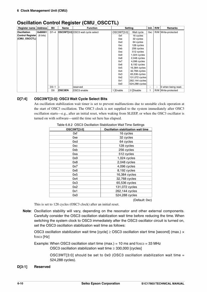
6 Clock Management Unit (CMU)
6-10 Seiko Epson Corporation S1C17803 TECHNICAL MANUAL
Oscillation Control Register (CMU_OSCCTL)Register name Address Bit Name Function Setting Init. R/W Remarks
Oscillation Control Register(CMU_OSCCTL)
0x80001(8 bits)
D7–4 OSC3WT[3:0] OSC3 wait cycle select OSC3WT[3:0] Wait cycle 0xc R/W Write-protected0xf0xe0xd0xc0xb0xa0x90x80x70x60x50x40x30x20x10x0
16 cycles32 cycles64 cycles128 cycles256 cycles512 cycles
1,024 cycles2,048 cycles4,096 cycles8,192 cycles
16,384 cycles32,768 cycles65,536 cycles
131,072 cycles262,144 cycles524,288 cycles
D3–1 – reserved – – – 0 when being read.D0 OSC3EN OSC3 enable 1 Enable 0 Disable 1 R/W Write-protected
D[7:4] OSC3WT[3:0]: OSC3 Wait Cycle Select Bits An oscillation stabilization wait timer is set to prevent malfunctions due to unstable clock operation at
the start of OSC3 oscillation. The OSC3 clock is not supplied to the system immediately after OSC3 oscillation starts—e.g., after an initial reset, when waking from SLEEP, or when the OSC3 oscillator is turned on with software—until the time set here has elapsed.
Table 6.8.2 OSC3 Oscillation Stabilization Wait Time SettingsOSC3WT[3:0] Oscillation stabilization wait time
0xf 16 cycles0xe 32 cycles0xd 64 cycles0xc 128 cycles0xb 256 cycles0xa 512 cycles0x9 1,024 cycles0x8 2,048 cycles0x7 4,096 cycles0x6 8,192 cycles0x5 16,384 cycles0x4 32,768 cycles0x3 65,536 cycles0x2 131,072 cycles0x1 262,144 cycles0x0 524,288 cycles
(Default: 0xc) This is set to 128 cycles (OSC3 clock) after an initial reset.
Note: Oscillation stability will vary, depending on the resonator and other external components. Carefully consider the OSC3 oscillation stabilization wait time before reducing the time. When switching the system clock to OSC3 immediately after the OSC3 oscillator circuit is turned on, set the OSC3 oscillation stabilization wait time as follows:
OSC3 oscillation stabilization wait time [cycle] ≥ OSC3 oscillation start time [second] (max.) × fOSC3 [Hz]
Example: When OSC3 oscillation start time (max.) = 10 ms and fOSC3 = 33 MHz OSC3 oscillation stabilization wait time ≥ 330,000 [cycles]
OSC3WT[3:0] should be set to 0x0 (OSC3 oscillation stabilization wait time = 524,288 cycles).
D[3:1] Reserved

6 Clock Management Unit (CMU)
S1C17803 TECHNICAL MANUAL Seiko Epson Corporation 6-11
D0 OSC3EN: OSC3 Enable Bit Enables or disables OSC3 oscillator operations. 1 (R/W): Enabled (on) (default) 0 (R/W): Disabled (off)
Note: The OSC3 oscillator cannot be stopped if the OSC3 clock is being used as the system clock.
Noise Filter Enable Register (CMU_NFEN)Register name Address Bit Name Function Setting Init. R/W Remarks
Noise Filter Enable Register(CMU_NFEN)
0x80002(8 bits)
D7–2 – reserved – – – 0 when being read.D1 DSINNFE DSIO input noise filter enable 1 Enable 0 Disable 0 R/W Write-protectedD0 NMINFE #NMI input noise filter enable 1 Enable 0 Disable 0 R/W
D[7:2] Reserved
D1 DSINNFE: DSIO Input Noise Filter Enable Bit Enables or disables the DSIO input noise filter. 1 (R/W): Enabled (noise filtering) 0 (R/W): Disabled (bypass) (default)
This noise filter inputs only DSIO pulses of not less than 16 cycles of the system clock (OSC3 or OSC1 clock) to the S1C17 Core. Pulses having widths of less than 16 cycles are filtered out as noise.
D0 NMINFE: #NMI Input Noise Filter Enable Bit Enables or disables the #NMI input noise filter. 1 (R/W): Enabled (noise filtering) 0 (R/W): Disabled (bypass) (default)
This noise filter inputs only NMI pulses of not less than 16 cycles of the system clock (OSC3 or OSC1 clock) to the S1C17 Core. Pulses having widths of less than 16 cycles are filtered out as noise.
LCDC Clock Setup Register (CMU_LCLK)Register name Address Bit Name Function Setting Init. R/W Remarks
LCDC Clock Setup Register(CMU_LCLK)
0x80003(8 bits)
D7–4 LCLKDIV[3:0] LCDC clock division ratio select LCLKDIV[3:0] Division ratio 0x7 R/W Write-protected0xf0xe0xd0xc0xb0xa0x90x80x70x60x50x40x30x20x10x0
OSC3•1/16OSC3•1/15OSC3•1/14OSC3•1/13OSC3•1/12OSC3•1/11OSC3•1/10OSC3•1/9OSC3•1/8OSC3•1/7OSC3•1/6OSC3•1/5OSC3•1/4OSC3•1/3OSC3•1/2OSC3•1/1
D3–1 – reserved – – – 0 when being read.D0 LCLK_EN LCLK clock enable 1 Enable 0 Disable 0 R/W Write-protected
D[7:4] LCLKDIV[3:0]: LCD Clock Division Ratio Select Bits Selects the LCDC clock (LCLK) from among 16 kinds of OSC3 division clocks. Select a clock accord-
ing to the frame rate.
fLCLK Frame rate = ————— [Hz] HT × VT
fLCLK: LCLK frequency HT: Horizontal total period (horizontal panel size + horizontal non-display period) [pixels] VT: Vertical total period (vertical panel size + vertical non-display period) [lines]

6 Clock Management Unit (CMU)
6-12 Seiko Epson Corporation S1C17803 TECHNICAL MANUAL
Table 6.8.3 LCDC Clock Division RatioLCLKDIV[3:0] LCLK
0xf OSC3•1/160xe OSC3•1/150xd OSC3•1/140xc OSC3•1/130xb OSC3•1/120xa OSC3•1/110x9 OSC3•1/100x8 OSC3•1/90x7 OSC3•1/80x6 OSC3•1/70x5 OSC3•1/60x4 OSC3•1/50x3 OSC3•1/40x2 OSC3•1/30x1 OSC3•1/20x0 OSC3•1/1
(Default: 0x7)
D0 LCLK_EN: LCLK Clock Enable Bit Enables or disables the LCLK clock supply to the LCD driver. 1 (R/W): Enabled (on) 0 (R/W): Disabled (off) (default)
The LCLK_EN default setting is 0, which stops the clock supply. Setting LCLK_EN to 1 supplies the clock selected as above to the LCD controller. If no LCD display is required, stop the clock supply to reduce current consumption.
Clock Control Register (CMU_CLKCTL)Register name Address Bit Name Function Setting Init. R/W Remarks
Clock Control Register(CMU_CLKCTL)
0x80004(8 bits)
D7–4 – reserved – – – 0 when being read.D3 BCLK_EN BCLK clock enable (in HALT) 1 Enable 0 Disable 1 R/W Write-protectedD2 PCLK2_EN PCLK2 clock enable 1 Enable 0 Disable 1 R/WD1 PCLK1_EN PCLK1 clock enable 1 Enable 0 Disable 1 R/WD0 PCLKSOC_EN PCLK_SOC clock enable 1 Enable 0 Disable 1 R/W
D[7:4] Reserved
D3 BCLK_EN: BCLK Clock Enable (in HALT) Bit Enables or disables the BCLK clock supply in HALT mode. 1 (R/W): Enabled (on) (default) 0 (R/W): Disabled (off)
The BCLK clock is used to operate the modules listed below.• IRAM/IVRAM• Bus matrix• SAPB bridge • SRAM controller (SRAMC)• Flash controller (FLASHC)• DMA controller (DMAC)• LCD controller (LCDC) bus interface and registers• Clock management unit (CMU) registers
BCLK is required for bus and memory operations, therefore, it is always supplied to the modules listed above in normal mode. However, the BCLK supply in HALT mode can be disabled to reduce current consumption by setting BCLK_EN to 1 if the LCDC and DMA do not need bus operations.

6 Clock Management Unit (CMU)
S1C17803 TECHNICAL MANUAL Seiko Epson Corporation 6-13
D2 PCLK2_EN: PCLK2 Clock Enable Bit Enables or disables the PCLK2 clock supply. 1 (R/W): Enabled (on) (default) 0 (R/W): Disabled (off) The PCLK2 clock is used to operate the modules listed below.
• Prescaler Ch.2 (PSC Ch.2)• 8-bit programmable timer Ch.1, Ch.2 (T8F Ch.1, Ch.2)• Universal serial interface Ch.1 (USI Ch.1) • A/D converter (ADC10)• I/O ports and port MUX (GPIO)• Watchdog timer (WDT)• Remote controller (REMC)• Card interface (CARD)• Real-time clock (RTC) registers• BBRAM
The PCLK2_EN default setting is 1, which enables the clock supply. If all the modules listed above can be stopped, disable the clock supply by setting PCLK2_EN to 0 to reduce current consumption.
D1 PCLK1_EN: PCLK1 Clock Enable Bit Enables or disables the PCLK1 clock supply. 1 (R/W): Enabled (on) (default) 0 (R/W): Disabled (off)
The PCLK1 clock is used to operate the modules listed below.• Prescaler Ch.1 (PSC Ch.1)• 8-bit programmable timer Ch.0 (T8F Ch.0)• 16-bit PWM timer (T16A)• 16-bit audio PWM timer (T16P)• Universal serial interface Ch.0 (USI Ch.0)• I2S (I2S)
The PCLK1_EN default setting is 1, which enables the clock supply. If all the modules listed above can be stopped, disable the clock supply by setting PCLK1_EN to 0 to reduce current consumption.
D0 PCLKSOC_EN: PCLK_SOC Clock Enable Bit Enables or disables the PCLK_SOC clock supply. 1 (R/W): Enabled (on) (default) 0 (R/W): Disabled (off)
The PCLK_SOC clock is used to operate the modules listed below.• Prescaler Ch.0 (PSC Ch.0)• Clock generator (CLG)• UART• I2C master (I2CM)• I2C Slave (I2CS)• Interrupt controller (ITC)
The PCLKSOC_EN default setting is 1, which enables the clock supply. If all the modules listed above can be stopped, disable the clock supply by setting PCLKSOC_EN to 0 to reduce current consumption.

6 Clock Management Unit (CMU)
6-14 Seiko Epson Corporation S1C17803 TECHNICAL MANUAL
System Clock Division Ratio Select Register (CMU_SYSCLKDIV)Register name Address Bit Name Function Setting Init. R/W Remarks
System Clock Division Ratio Select Register(CMU_SYSCLKDIV)
0x80005(8 bits)
D7–3 – reserved – – – 0 when being read.D2–0 SYSCLKDIV
[2:0]System clock division ratio select SYSCLKDIV[2:0] Divider 0x0 R/W Write-protected
0x7–0x60x50x40x30x20x10x0
OSC•1/1OSC•1/32OSC•1/16OSC•1/8OSC•1/4OSC•1/2OSC•1/1
D[7:3] Reserved
D[2:0] SYSCLKDIV[2:0]: System Clock Division Ratio Select Bits Selects a division ratio to set the system clock frequency. To reduce current consumption, operate the
S1C17 Core and peripheral modules using the slowest possible clock speed.
Table 6.8.4 System Clock Division RatioSYSCLKDIV[2:0] System clock source
0x7–0x6 OSC•1/10x5 OSC•1/320x4 OSC•1/160x3 OSC•1/80x2 OSC•1/40x1 OSC•1/20x0 OSC•1/1
(Default: 0x0)
CMU_CLK Select Register (CMU_CMUCLK)Register name Address Bit Name Function Setting Init. R/W Remarks
CMU_CLK Select Register(CMU_CMUCLK)
0x80006(8 bits)
D7–4 – reserved – – – 0 when being read.D3–0 CMU_
CLKSEL[3:0]CMU_CLK select CMU_CLKSEL[3:0] CMU_CLK 0x0 R/W Write-protected
0xf–0x80x70x60x50x40x30x20x10x0
reservedLCLK
PCLK2PCLK1
PCLK_SOCBCLKCCLKOSC1OSC3
D[7:4] Reserved
D[3:0] CMU_CLKSEL[3:0]: CMU_CLK Select Bits Selects an internally generated clock to be output from the CMU_CLK pin to external devices.
Table 6.8.5 Selecting CMU_CLKCMU_CLKSEL[3:0] CMU_CLK
0xf–0x8 Reserved0x7 LCLK0x6 PCLK20x5 PCLK10x4 PCLK_SOC0x3 BCLK0x2 CCLK0x1 OSC10x0 OSC3
(Default: 0x0)
CMU_CLK can be selected at any time. However, switching over the clocks creates hazards.
Note: Settings other than those listed in Table 6.8.5 are reserved for testing. Do not set undescribed val-ues to CMU_CLKSEL[3:0] as undesired clocks may output.

6 Clock Management Unit (CMU)
S1C17803 TECHNICAL MANUAL Seiko Epson Corporation 6-15
MAC Wait Cycle Select Register (MAC_WAIT)Register name Address Bit Name Function Setting Init. R/W Remarks
MAC Wait Cycle Select Register(MAC_WAIT)
0x80007(8 bits)
D7–1 – reserved – – – 0 when being read.
D0 MACWAIT MAC wait cycle select 1 1 cycle 0 0 cycles 0 R/W Write-protected
D[7:1] Reserved
D0 MACWAIT: MAC Wait Cycle Select Bit Selects the number of wait cycles to be inserted when the multiplier/divider module is accessed. 1 (R/W): 1 cycle 0 (R/W): 0 cycles (default)
If the system clock frequency is lower than 24 MHz, 0 wait cycles can be selected.
CMU Write Protect Register (CMU_PROTECT)Register name Address Bit Name Function Setting Init. R/W Remarks
CMU Write Protect Register(CMU_PROTECT)
0x80010(8 bits)
D7–0 CMUP[7:0] CMU register protect flag Writing 10010110 (0x96) removes the write protection of the CMU registers (0x80000–0x80007).Writing another value set the write protection.
0x0 R/W
D[7:0] CMUP[7:0]: CMU Register Protect Flag Bits Enables or disables write protection of the CMU control registers (0x80000–0x80007). 0x96 (R/W): Disable write protection Other than 0x96 (R/W): Write-protect the register (default: 0x0)
Before altering any CMU control register, write data 0x96 to CMUP[7:0] to disable write protection. If CMUP[7:0] is set to other than 0x96, even if an attempt is made to alter any CMU control register by executing a write instruction, the content of the register will not be altered even though the instruction may have been executed without a problem. Once CMUP[7:0] is set to 0x96, the CMU control registers can be rewritten any number of times until being reset to other than 0x96. When rewriting the CMU control registers has finished, CMUP[7:0] should be set to other than 0x96 to prevent accidental writing to the CMU registers.

7 Prescaler (PSC)
S1C17803 TECHNICAL MANUAL Seiko Epson Corporation 7-1
7 Prescaler (PSC)
7.1 PSC Module OverviewThe S1C17803 incorporates a prescaler (PSC) module to generate clocks for timer and serial interface operations. The PSC module consists of three frequency dividers (PSC Ch.0, PSC Ch.1, and PSC Ch.2) that generate 15 dif-ferent frequencies by dividing the PCLK_SOC, PCLK1 and PCLK2 clock supplied from the clock management unit (CMU) into 1/1 to 1/16K. The peripheral modules to which the clock is supplied include clock-select registers enabling selection of one as a count or operation clock.
1/1PCLK1
Debug status signal
PSC Ch.11/2 1/4 1/8 1/16 1/32 1/64 1/128
1/256 1/512 1/1K 1/2K 1/4K 1/8K 1/16K
USI Ch.0
16-bit PWM timer16-bit audio PWM timer8-bit programmable timer Ch.0
1/1PCLK_SOC
Debug status signal
PSC Ch.01/2 1/4 1/8 1/16 1/32 1/64 1/128
1/256 1/512 1/1K 1/2K 1/4K 1/8K 1/16K
UARTI2C master
Clock generator
1/1PCLK2
Debug status signal
PSC Ch.21/2 1/4 1/8 1/16 1/32 1/64 1/128
1/256 1/512 1/1K 1/2K 1/4K 1/8K 1/16K
USI Ch.1A/D converter trigger
GPIORemote controllerA/D converter
8-bit programmable timer Ch.18-bit programmable timer Ch.2
Figure 7.1.1 Prescaler Configuration
PSC Ch.0 is controlled by PRUN/PSC_CTL0 register. PSC Ch.1 and PSC Ch.2 are controlled by PRUN/PSC_CTL1 register. To operate the prescaler, write 1 to PRUN. Writing 0 to PRUN stops the prescaler. Stopping the prescaler while the timer and interface modules are halted enables the current consumption to be reduced. The pres-caler is stopped at initial reset.
Note: PCLK_SOC, PCLK1, and PCLK2 must be supplied from the CMU to use the PSC Ch.0, PSC Ch.1, and PSC Ch.2, respectively.
The prescaler features another control bit, PRUND/PSC_CTLx register, which specifies prescaler operations in debug mode. Setting PRUND to 1 operates the prescaler in debug mode. Setting it to 0 stops the prescaler when the S1C17 Core enters debug mode. Set PRUND to 1 when operating the timer and interface modules during debug-ging.
7.2 Control Register Details
Table 7.2.1 PSC RegistersAddress Register name Function
0x4020 PSC_CTL0 PSC Ch.0 Control Register Starts/stops the PSC Ch.0.0x80300 PSC_CTL1 PSC Ch.1–2 Control Register Starts/stops the PSC Ch.1 and PSC Ch.2.
The prescaler registers are an 8-bit register.
Note: When data is written to the register, the “Reserved” bits must always be written as 0 and not 1.

7 Prescaler (PSC)
7-2 Seiko Epson Corporation S1C17803 TECHNICAL MANUAL
PSC Ch.0 Control Register (PSC_CTL0)Register name Address Bit Name Function Setting Init. R/W Remarks
PSC Ch.0 Control Register(PSC_CTL0)
0x4020(8 bits)
D7–2 – reserved – – – 0 when being read.D1 PRUND PSC Ch.0 run/stop in debug mode 1 Run 0 Stop 0 R/WD0 PRUN PSC Ch.0 run/stop control 1 Run 0 Stop 0 R/W
D[7:2] Reserved
D1 PRUND: PSC Ch.0 Run/Stop in Debug Mode Bit Selects PSC Ch.0 operations in debug mode. 1 (R/W): Run 0 (R/W): Stop (default)
Setting PRUND to 1 operates PSC Ch.0 even in debug mode. Setting it to 0 stops PSC Ch.0 when the S1C17 Core enters debug mode. Set PRUND to 1 to use the modules listed below during debugging.
D0 PRUN: PSC Ch.0 Run/Stop Control Bit Starts or stops PSC Ch.0. 1 (R/W): Start operation 0 (R/W): Stop (default)
Write 1 to PRUN to operate PSC Ch.0. Write 0 to PRUN to stop PSC Ch.0. To reduce current consump-tion, stop PSC Ch.0 if the modules listed below are already stopped.
Modules that use PSC Ch.0 output clocks • CLG_T16FU0 (clock source for UART) • CLG_T8I (clock source for I2C master)
PSC Ch.1–2 Control Register (PSC_CTL1)Register name Address Bit Name Function Setting Init. R/W Remarks
PSC Ch.1–2 Control Register(PSC_CTL1)
0x80300(8 bits)
D7–2 – reserved – – – 0 when being read.D1 PRUND PSC Ch.1–2 run/stop in debug
mode1 Run 0 Stop 0 R/W
D0 PRUN PSC Ch.1–2 run/stop control 1 Run 0 Stop 0 R/W
D[7:2] Reserved
D1 PRUND: PSC Ch.1–2 Run/Stop in Debug Mode Bit Selects PSC Ch.1 and PSC Ch.2 operations in debug mode. 1 (R/W): Run 0 (R/W): Stop (default)
Setting PRUND to 1 operates PSC Ch.1 and PSC Ch.2 even in debug mode. Setting it to 0 stops PSC Ch.1 and PSC Ch.2 when the S1C17 Core enters debug mode. Set PRUND to 1 to use the modules listed below during debugging.
D0 PRUN: PSC Ch.1–2 Run/Stop Control Bit Starts or stops PSC Ch.1 and PSC Ch.2. 1 (R/W): Start operation 0 (R/W): Stop (default)
Write 1 to PRUN to operate PSC Ch.1 and PSC Ch.2. Write 0 to PRUN to stop PSC Ch.1 and PSC Ch.2. To reduce current consumption, stop PSC Ch.1 and PSC Ch.2 if the modules listed below are al-ready stopped.
Modules that use PSC Ch.1 output clocks • 16-bit PWM timer • 16-bit audio PWM timer • 8-bit programmable timer Ch.0 (clock source for USI Ch.0)

7 Prescaler (PSC)
S1C17803 TECHNICAL MANUAL Seiko Epson Corporation 7-3
Modules that use PSC Ch.2 output clocks • 8-bit programmable timer Ch.1 (clock source for USI Ch.1) • 8-bit programmable timer Ch.2 (trigger source for A/D converter) • A/D converter • Remote controller • I/O ports

8 Clock Generator (CLG)
S1C17803 TECHNICAL MANUAL Seiko Epson Corporation 8-1
8 Clock Generator (CLG)
8.1 CLG Module OverviewThe S1C17803 is equipped with a clock generator (CLG) that consists of a 16-bit timer with fine mode (CLG_T16FU0) and an 8-bit timer (CLG_T8I).The features of the CLG module are listed below.
• CLG_T16FU0 generates the UART operating clock (transfer clock source).
• CLG_T8I generates the I2C master operating clocks (transfer clock/sampling clock source).
• Any desired serial transfer rates can be programmed.
• Uses prescaler (PSC Ch.0) as the clock source.
Figure 8.1.1 shows the configuration of the clock generator.
1/1PCLK_SOC
Prescaler(PSC Ch.0) 16-bit timer
with fine mode[CLG_T16FU0]
CLG
1/16K
UART
Timer underflow interrupt to ITC
8-bit timer[CLG_T8I] I2C master (I2CM)
Timer underflow interrupt to ITC
•••
•••
•••
Figure 8.1.1 Configuration of the Clock Generator
When the serial interface is not used, the timer can be used as a general-purpose programmable timer with an inter-rupt function.

8 Clock Generator (CLG)
8-2 Seiko Epson Corporation S1C17803 TECHNICAL MANUAL
8.2 16-bit Timer with Fine Mode (CLG_T16FU0)
8.2.1 CLG_T16FU0 Overview
The CLG module incorporates a 16-bit timer with fine mode (CLG_T16FU0).The features of CLG_T16FU0 are listed below.
• 16-bit presettable down counter with a 16-bit reload data register for setting the preset value
• The count clock is selectable from 15 clocks output from the prescaler (PSC Ch.0).
• Generates the UART operating clock (transfer clock source) from the counter underflow signal.
• Generates an underflow interrupt signal to the interrupt controller (ITC).
• Any desired time intervals and serial transfer rates can be programmed by selecting an appropriate count clock and preset value.
• Fine mode is provided to minimize transfer rate errors.
Figure 8.2.1.1 shows the CLG_T16FU0 configuration.
Reload data registerT16FU0_TR
PRUN
DF[3:0]
PCLK_SOC•1/1–1/16K
Underflow
Run/stop control
Inte
rnal
dat
a bu
s
Count clock select
Interrupt request
Serial transfer clock
To ITCTo UART
PRESER Timer reset
TFMD[3:0] Fine mode setting
Down counterT16FU0_TC
Control circuit
Count mode select TRMD
Prescaler
16-bit timer with fine mode(CLG_T16FU0)
Figure 8.2.1.1 CLG_T16FU0 Configuration
CLG_T16FU0 consists of a 16-bit presettable down counter and a 16-bit reload data register holding the preset val-ue. The timer counts down from the initial value set in the reload data register and outputs an underflow signal when the counter underflows. The underflow signal is used to generate an interrupt and UART clock. The underflow cycle can be programmed by selecting the prescaler clock and reload data, enabling the application program to obtain time intervals and serial transfer rates as required. Fine mode provides a function that minimizes transfer rate errors.
8.2.2 Count Clock
The count clock is selected by DF[3:0]/CLG_T16FU0_CLK register from the 15 types generated by prescaler (PSC Ch.0) dividing the PCLK_SOC clock into 1/1 to 1/16K.
Table 8.2.2.1 Count Clock SelectionDF[3:0] PSC Ch.0 output clock DF[3:0] PSC Ch.0 output clock
0xf Reserved 0x7 PCLK_SOC•1/1280xe PCLK_SOC•1/16384 0x6 PCLK_SOC•1/640xd PCLK_SOC•1/8192 0x5 PCLK_SOC•1/320xc PCLK_SOC•1/4096 0x4 PCLK_SOC•1/160xb PCLK_SOC•1/2048 0x3 PCLK_SOC•1/80xa PCLK_SOC•1/1024 0x2 PCLK_SOC•1/40x9 PCLK_SOC•1/512 0x1 PCLK_SOC•1/20x8 PCLK_SOC•1/256 0x0 PCLK_SOC•1/1
(Default: 0x0)
Notes: • Before CLG_T16FU0 can start counting, PSC Ch.0 must be run.
• Make sure the counter is halted before setting the count clock.
For controlling PSC Ch.0, refer to the “Prescaler (PSC)” chapter.

8 Clock Generator (CLG)
S1C17803 TECHNICAL MANUAL Seiko Epson Corporation 8-3
8.2.3 Count Mode
CLG_T16FU0 features two count modes: repeat mode and one-shot mode. These modes are selected using TRMD/CLG_T16FU0_CTL register.
Repeat mode (TRMD = 0, default) Setting TRMD to 0 sets CLG_T16FU0 to repeat mode. In this mode, once the count starts, the timer continues running until stopped by the application program. When
the counter underflows, the timer presets the reload data register value into the counter and continues the count. Thus, the timer periodically outputs an underflow pulse. CLG_T16FU0 should be set to this mode to generate periodic interrupts at desired intervals or to generate a serial transfer clock.
One-shot mode (TRMD = 1) Setting TRMD to 1 sets CLG_T16FU0 to one-shot mode. In this mode, the timer stops automatically as soon as the counter underflows. This means only one interrupt
can be generated after the timer starts. Note that the timer presets the reload data register value to the counter, then stops after an underflow has occurred. CLG_T16FU0 should be set to this mode to set a specific wait time.
Note: Make sure the counter is halted before setting the count mode.
8.2.4 Reload Register and Underflow Period
The reload data register (CLG_T16FU0_TR) is used to set the initial value for the down counter.The initial counter value set in the reload data register is preset to the down counter if the timer is reset or the coun-ter underflows. If the timer is started after resetting, it counts down from the reload value (initial value). This means that the reload value and the input clock frequency determine the time elapsed from the point at which the timer starts until the underflow occurs (or between underflows). The time determined is used to obtain the specified wait time, the intervals between periodic interrupts, and the programmable serial interface transfer clock.
One-shot mode
Counter
Repeat mode
Counter
01n-1n n
Preset by resetting the timer
Preset by resetting the timer
Preset automatically
Underflow
Preset automatically
(n = Reload data)
01n-1n n
Underflow
Timer starts
Timer starts
Preset automatically
01n-1 n
Underflow
Figure 8.2.4.1 Preset Timing
The underflow cycle can be calculated as follows:
TR + 1 clk_inUnderflow interval = ———— [s] Underflow cycle = ———— [Hz] clk_in TR + 1
clk_in: Count clock (PSC Ch.0 output clock) frequency [Hz]TR: Reload data (0–65535)
Note: The UART divides the CLG_T16FU0 output by 16 to generate the sampling clock. Be careful when setting the transfer rate.
8.2.5 Timer Reset
CLG_T16FU0 is reset by writing 1 to PRESER/CLG_T16FU0_CTL register. The reload data is preset and the counter is initialized.

8 Clock Generator (CLG)
8-4 Seiko Epson Corporation S1C17803 TECHNICAL MANUAL
8.2.6 Run/Stop Control
Make the following settings before starting CLG_T16FU0.(1) Select the count clock (PSC Ch.0 output clock). See Section 8.2.2.(2) Set the count mode (one-shot or repeat). See Section 8.2.3.(3) Calculate the initial counter value and set it to the reload data register. See Section 8.2.4.(4) Reset the timer to preset the counter to the initial value. See Section 8.2.5.(5) When using timer interrupts, set the interrupt level and enable the interrupt. See Section 8.2.9.
To start CLG_T16FU0, write 1 to PRUN/CLG_T16FU0_CTL register.The timer starts counting down from the initial value or from the current counter value if no initial value was preset. When the counter underflows, the timer outputs an underflow pulse and presets the counter to the initial value. An interrupt request is sent simultaneously to the interrupt controller (ITC).If one-shot mode is set, the timer stops counting.If repeat mode is set, the timer continues counting from the reloaded initial value.
Write 0 to PRUN to stop CLG_T16FU0_CTL via the application program. The counter stops counting and retains the current counter value until either the timer is reset or restarted. To restart the count from the initial value, the timer should be reset before writing 1 to PRUN.When the timer is reset during running, the timer loads the reload register value to the counter and continues count-ing.
Count clock
PRESER write
PRUN
Counter
Interrupt request
01n-1n n
Count clock
PRESER write
PRUN
Counter
Interrupt request
01n-1n n 01n-1 n n-1
One-shot mode
Repeat mode
Reset by hardwareSet by software
Set by software Reset by software
Table 8.2.6.1 Count Operation
8.2.7 CLG_T16FU0 Output Signal
CLG_T16FU0 outputs underflow pulses when the counter underflows. These pulses are used for timer interrupt requests.These pulses are also used to generate the serial transfer clock for UART.
Underflow signal
Timer output(serial transfer clock)
Interrupt request to the ITC
Figure 8.2.7.1 Timer Output Clock

8 Clock Generator (CLG)
S1C17803 TECHNICAL MANUAL Seiko Epson Corporation 8-5
Use the following equations to calculate the reload data register value for obtaining the desired transfer rate.
clk_inbps = ———————————— {(TR + 1) × 16 + TFMD} clk_inTR = (——— - TFMD - 16) ÷ 16 bps
clk_in: Count clock (PSC Ch.0 output clock) frequency (Hz)TR: Reload data (0–65535)bps: Transfer rate (bit/s)TFMD: Fine mode setting (0 to 15)
8.2.8 Fine Mode
Fine mode provides a function that minimizes transfer rate errors.CLG_T16FU0 can output a programmable clock signal for use as the UART serial transfer clock. The timer output clock can be set to the required frequency by selecting the appropriate PSC Ch.0 output clock and reload data. Note that errors may occur, depending on the transfer rate. Fine mode extends the output clock cycle by delaying the un-derflow pulse from the counter. This delay can be specified with the TFMD[3:0]/CLG_T16FU0_CTL register.TFMD[3:0] specifies the delay pattern to be inserted into a 16 underflow period. Inserting one delay extends the output clock cycle by one count clock cycle. This setting delays the interrupt timing in the same way.
Table 8.2.8.1 Delay Patterns Specified by TFMD[3:0]
TFMD[3:0]Underflow number
1 2 3 4 5 6 7 8 9 10 11 12 13 14 15 16
0x0 – – – – – – – – – – – – – – – –0x1 – – – – – – – – – – – – – – – D0x2 – – – – – – – D – – – – – – – D0x3 – – – – – – – D – – – D – – – D0x4 – – – D – – – D – – – D – – – D0x5 – – – D – – – D – – – D – D – D0x6 – – – D – D – D – – – D – D – D0x7 – – – D – D – D – D – D – D – D0x8 – D – D – D – D – D – D – D – D0x9 – D – D – D – D – D – D – D D D0xa – D – D – D D D – D – D – D D D0xb – D – D – D D D – D D D – D D D0xc – D D D – D D D – D D D – D D D0xd – D D D – D D D – D D D D D D D0xe – D D D D D D D – D D D D D D D0xf – D D D D D D D D D D D D D D D
D: Indicates the insertion of a delay cycle.
Count clock
Underflow signal (not corrected)
Underflow signal (corrected)
Output clock (not corrected)
Output clock (corrected)
Delayed
15 16
15 16
1
1
Figure 8.2.8.1 Delay Cycle Insertion in Fine Mode
At initial reset, TFMD[3:0] is set to 0x0, preventing insertion of delay cycles.

8 Clock Generator (CLG)
8-6 Seiko Epson Corporation S1C17803 TECHNICAL MANUAL
8.2.9 CLG_T16FU0 Interrupt
CLG_T16FU0 outputs an interrupt request to the interrupt controller (ITC) when the counter underflows.
Timer underflow interrupt When the counter underflows, the interrupt flag T16FU0IF/CLG_T16FU0_INT register is set to 1. At the same
time, an interrupt request is sent to the ITC if T16FU0IE/CLG_T16FU0_INT register has been set to 1 (interrupt enabled). An interrupt is generated if the ITC and S1C17 Core interrupt conditions are satisfied.
If T16FU0IE is set to 0 (interrupt disabled, default), no interrupt request will be sent to the ITC. For specific information on interrupt processing, see the “Interrupt Controller (ITC)” chapter.
Notes: • The CLG_T16FU0 interrupt flag T16FU0IF must be reset in the interrupt handler routine after a CLG_T16FU0 interrupt has occurred to prevent recurring interrupts.
• Reset T16FU0IF before enabling CLG_T16FU0 interrupts with T16FU0IE to prevent occur-rence of unwanted interrupt. T16FU0IF is reset by writing 1.
8.2.10 Details of Control RegistersTable 8.2.10.1 List of CLG_T16FU0 Registers
Address Register name Function0x4200 CLG_T16FU0_CLK CLG_T16FU0 Input Clock Select Register Selects a prescaler output clock.0x4202 CLG_T16FU0_TR CLG_T16FU0 Reload Data Register Sets reload data.0x4204 CLG_T16FU0_TC CLG_T16FU0 Counter Data Register Counter data0x4206 CLG_T16FU0_CTL CLG_T16FU0 Control Register Sets the timer mode and starts/stops the timer.0x4208 CLG_T16FU0_INT CLG_T16FU0 Interrupt Control Register Controls the interrupt.
The following describes each CLG_T16FU0 register. These are all 16-bit registers.
Note: When data is written to the register, the “Reserved” bits must always be written as 0 and not 1.
CLG_T16FU0 Input Clock Select Register (CLG_T16FU0_CLK)Register name Address Bit Name Function Setting Init. R/W Remarks
CLG_T16FU0 Input Clock Select Register(CLG_T16FU0_CLK)
0x4200(16 bits)
D15–4 – reserved – – – 0 when being read.D3–0 DF[3:0] CLG_T16FU0 input clock select
(PSC Ch.0 output clock)DF[3:0] Clock 0x0 R/W
0xf0xe0xd0xc0xb0xa0x90x80x70x60x50x40x30x20x10x0
reservedPCLK_SOC•1/16384PCLK_SOC•1/8192PCLK_SOC•1/4096PCLK_SOC•1/2048PCLK_SOC•1/1024PCLK_SOC•1/512PCLK_SOC•1/256PCLK_SOC•1/128PCLK_SOC•1/64PCLK_SOC•1/32PCLK_SOC•1/16PCLK_SOC•1/8PCLK_SOC•1/4PCLK_SOC•1/2PCLK_SOC•1/1
D[15:4] Reserved
D[3:0] DF[3:0]: CLG_T16FU0 Input Clock Select Bits Selects the CLG_T16FU0 count clock from the 15 different prescaler output clocks.

8 Clock Generator (CLG)
S1C17803 TECHNICAL MANUAL Seiko Epson Corporation 8-7
Table 8.2.10.2 Count Clock SelectionDF[3:0] Prescaler output clock DF[3:0] Prescaler output clock
0xf Reserved 0x7 PCLK_SOC•1/1280xe PCLK_SOC•1/16384 0x6 PCLK_SOC•1/640xd PCLK_SOC•1/8192 0x5 PCLK_SOC•1/320xc PCLK_SOC•1/4096 0x4 PCLK_SOC•1/160xb PCLK_SOC•1/2048 0x3 PCLK_SOC•1/80xa PCLK_SOC•1/1024 0x2 PCLK_SOC•1/40x9 PCLK_SOC•1/512 0x1 PCLK_SOC•1/20x8 PCLK_SOC•1/256 0x0 PCLK_SOC•1/1
(Default: 0x0)
Note: Make sure the counter is halted before setting the count clock.
CLG_T16FU0 Reload Data Register (CLG_T16FU0_TR)Register name Address Bit Name Function Setting Init. R/W Remarks
CLG_T16FU0 Reload Data Register(CLG_T16FU0_TR)
0x4202(16 bits)
D15–0 TR[15:0] CLG_T16FU0 reload dataTR15 = MSBTR0 = LSB
0x0 to 0xffff 0x0 R/W
D[15:0] TR[15:0]: CLG_T16FU0 Reload Data Bits Sets the counter initial value. (Default: 0x0) The reload data set in this register is preset to the counter when the timer is reset or the counter under-
flows. If the timer is started after resetting, it counts down from the reload value (initial value). This means that the reload value and the input clock frequency determine the time elapsed from the point at which the timer starts until the underflow occurs (or between underflows). The time determined is used to obtain the desired wait time, the intervals between periodic interrupts, and the programmable serial interface transfer clock.
CLG_T16FU0 Counter Data Register (CLG_T16FU0_TC)Register name Address Bit Name Function Setting Init. R/W Remarks
CLG_T16FU0 Counter Data Register(CLG_T16FU0_TC)
0x4204(16 bits)
D15–0 TC[15:0] CLG_T16FU0 counter dataTC15 = MSBTC0 = LSB
0x0 to 0xffff 0xffff R
D[15:0] TC[15:0]: CLG_T16FU0 Counter Data Bits The counter data can be read out. (Default: 0xffff) This register is read-only and cannot be written to.
CLG_T16FU0 Control Register (CLG_T16FU0_CTL)Register name Address Bit Name Function Setting Init. R/W Remarks
CLG_T16FU0 Control Register(CLG_T16FU0_CTL)
0x4206(16 bits)
D15–12 – reserved – – – 0 when being read.D11–8 TFMD[3:0] Fine mode setup 0x0 to 0xf 0x0 R/W Set a number of times
to insert delay into a 16-underflow period.
D7–5 – reserved – – – 0 when being read.D4 TRMD Count mode select 1 One shot 0 Repeat 0 R/W
D3–2 – reserved – – – 0 when being read.D1 PRESER Timer reset 1 Reset 0 Ignored 0 WD0 PRUN Timer run/stop control 1 Run 0 Stop 0 R/W
D[15:12] Reserved
D[11:8] TFMD[3:0]: Fine Mode Setup Bits Corrects the transfer rate error. (Default: 0x0) TFMD[3:0] specifies the delay pattern to be inserted into a 16 underflow period. Inserting one delay
extends the output clock cycle by one count clock cycle. This setting delays the interrupt timing in the same way.

8 Clock Generator (CLG)
8-8 Seiko Epson Corporation S1C17803 TECHNICAL MANUAL
Table 8.2.10.3 Delay Patterns Specified by TFMD[3:0]
TFMD[3:0]Underflow number
1 2 3 4 5 6 7 8 9 10 11 12 13 14 15 16
0x0 – – – – – – – – – – – – – – – –0x1 – – – – – – – – – – – – – – – D0x2 – – – – – – – D – – – – – – – D0x3 – – – – – – – D – – – D – – – D0x4 – – – D – – – D – – – D – – – D0x5 – – – D – – – D – – – D – D – D0x6 – – – D – D – D – – – D – D – D0x7 – – – D – D – D – D – D – D – D0x8 – D – D – D – D – D – D – D – D0x9 – D – D – D – D – D – D – D D D0xa – D – D – D D D – D – D – D D D0xb – D – D – D D D – D D D – D D D0xc – D D D – D D D – D D D – D D D0xd – D D D – D D D – D D D D D D D0xe – D D D D D D D – D D D D D D D0xf – D D D D D D D D D D D D D D D
D: Indicates the insertion of a delay cycle.
Count clock
Underflow signal (not corrected)
Underflow signal (corrected)
Output clock (not corrected)
Output clock (corrected)
Delayed
15 16
15 16
1
1
Figure 8.2.10.1 Delay Cycle Insertion in Fine Mode
D[7:5] Reserved
D4 TRMD: Count Mode Select Bit Selects the CLG_T16FU0 count mode. 1 (R/W): One-shot mode 0 (R/W): Repeat mode (default)
Setting TRMD to 0 sets CLG_T16FU0 to repeat mode. In this mode, once the count starts, the timer continues to run until stopped by the application program. When the counter underflows, the timer pre-sets the counter to the reload data register value and continues the count. Thus, the timer periodically outputs an underflow pulse. Set CLG_T16FU0 to this mode to generate periodic interrupts at desired intervals or to generate a serial transfer clock.
Setting TRMD to 1 sets CLG_T16FU0 to one-shot mode. In this mode, the timer stops automatically as soon as the counter underflows. This means only one interrupt can be generated after the timer starts. Note that the timer presets the counter to the reload data register value, then stops when an underflow occurs. Set CLG_T16FU0 to this mode to set a specific wait time.
Note: Make sure the counter is halted before setting the count mode.
D[3:2] Reserved
D1 PRESER: Timer Reset Bit Resets CLG_T16FU0. 1 (W): Reset 0 (W): Ignored 0 (R): Always 0 when read (default)
Writing 1 to this bit presets the counter to the reload data value.

8 Clock Generator (CLG)
S1C17803 TECHNICAL MANUAL Seiko Epson Corporation 8-9
D0 PRUN: Timer Run/Stop Control Bit Controls the timer RUN/STOP. 1 (R/W): Run 0 (R/W): Stop (default)
The timer starts counting when PRUN is written as 1 and stops when written as 0. When the timer is stopped, the counter data is retained until reset or until the next RUN state.
CLG_T16FU0 Interrupt Control Register (CLG_T16FU0_INT)Register name Address Bit Name Function Setting Init. R/W Remarks
CLG_T16FU0 Interrupt Control Register(CLG_T16FU0_INT)
0x4208(16 bits)
D15–9 – reserved – – – 0 when being read.D8 T16FU0IE CLG_T16FU0 interrupt enable 1 Enable 0 Disable 0 R/W
D7–1 – reserved – – – 0 when being read.D0 T16FU0IF CLG_T16FU0 interrupt flag 1 Cause of
interrupt occurred
0 Cause of interrupt not occurred
0 R/W Reset by writing 1.
D[15:9] Reserved
D8 T16FU0IE: CLG_T16FU0 Interrupt Enable Bit Enables or disables interrupts caused by counter underflows. 1 (R/W): Interrupt enabled 0 (R/W): Interrupt disabled (default)
Setting T16FU0IE to 1 enables CLG_T16FU0 interrupt requests to the ITC; setting to 0 disables inter-rupts.
D[7:1] Reserved
D0 T16FU0IF: CLG_T16FU0 Interrupt Flag Bit Indicates whether the cause of counter underflow interrupt has occurred or not. 1 (R): Cause of interrupt has occurred 0 (R): No cause of interrupt has occurred (default) 1 (W): Flag is reset 0 (W): Ignored
T16FU0IF is the CLG_T16FU0 interrupt flag that is set to 1 when the counter underflows. T16FU0IF is reset by writing 1.

8 Clock Generator (CLG)
8-10 Seiko Epson Corporation S1C17803 TECHNICAL MANUAL
8.3 8-bit Timer (CLG_T8I)
8.3.1 CLG_T8I Overview
The CLG module incorporates an 8-bit timer (CLG_T8I).The features of CLG_T8I are listed below.
• 8-bit presettable down counter with an 8-bit reload data register for setting the preset value
• The count clock is selectable from 15 clocks output from the prescaler (PSC Ch.0).
• Generates the I2C master operating clock from the counter underflow signal.
• Generates an underflow interrupt signal to the interrupt controller (ITC).
• Any desired time intervals and serial transfer rates can be programmed by selecting an appropriate count clock and preset value.
Figure 8.3.1.1 shows the CLG_T8I configuration.
Reload data registerT8I_TR
PRUN
DF[3:0]
PCLK_SOC•1/1–1/16K
Underflow
Run/stop control
Inte
rnal
dat
a bu
s
Count clock select
Interrupt request
Serial transfer clock
To ITCTo I2C master
PRESER Timer reset
Down counterT8I_TC
Control circuit
Count mode select TRMD
Prescaler
8-bit timer (CLG_T8I)
Figure 8.3.1.1 CLG_T8I Configuration
CLG_T8I consists of an 8-bit presettable down counter and an 8-bit reload data register holding the preset value. The timer counts down from the initial value set in the reload data register and outputs an underflow signal when the counter underflows. The underflow signal is used to generate an interrupt and I2C master clock. The underflow cycle can be programmed by selecting the prescaler clock and reload data, enabling the application program to obtain time intervals and serial transfer rates as required.
8.3.2 Count Clock
The count clock is selected by DF[3:0]/CLG_T8I_CLK register from the 15 types generated by prescaler (PSC Ch.0) dividing the PCLK_SOC clock into 1/1 to 1/16K.
Table 8.3.2.1 Count Clock SelectionDF[3:0] PSC Ch.0 output clock DF[3:0] PSC Ch.0 output clock
0xf Reserved 0x7 PCLK_SOC•1/1280xe PCLK_SOC•1/16384 0x6 PCLK_SOC•1/640xd PCLK_SOC•1/8192 0x5 PCLK_SOC•1/320xc PCLK_SOC•1/4096 0x4 PCLK_SOC•1/160xb PCLK_SOC•1/2048 0x3 PCLK_SOC•1/80xa PCLK_SOC•1/1024 0x2 PCLK_SOC•1/40x9 PCLK_SOC•1/512 0x1 PCLK_SOC•1/20x8 PCLK_SOC•1/256 0x0 PCLK_SOC•1/1
(Default: 0x0)
Notes: • Before CLG_T8I can start counting, PSC Ch.0 must be run.
• Make sure the counter is halted before setting the count clock.
For controlling PSC Ch.0, refer to the “Prescaler (PSC)” chapter.

8 Clock Generator (CLG)
S1C17803 TECHNICAL MANUAL Seiko Epson Corporation 8-11
8.3.3 Count Mode
CLG_T8I features two count modes: repeat mode and one-shot mode. These modes are selected using TRMD/CLG_T8I_CTL register.
Repeat mode (TRMD = 0, default) Setting TRMD to 0 sets CLG_T8I to repeat mode. In this mode, once the count starts, the timer continues running until stopped by the application program. When
the counter underflows, the timer presets the reload data register value into the counter and continues the count. Thus, the timer periodically outputs an underflow pulse. CLG_T8I should be set to this mode to generate peri-odic interrupts at desired intervals or to generate a serial transfer clock.
One-shot mode (TRMD = 1) Setting TRMD to 1 sets CLG_T8I to one-shot mode. In this mode, the timer stops automatically as soon as the counter underflows. This means only one interrupt
can be generated after the timer starts. Note that the timer presets the reload data register value to the counter, then stops after an underflow has occurred. CLG_T8I should be set to this mode to set a specific wait time.
Note: Make sure the counter is halted before setting the count mode.
8.3.4 Reload Register and Underflow Period
The reload data register (CLG_T8I_TR) is used to set the initial value for the down counter.The initial counter value set in the reload data register is preset to the down counter if the timer is reset or the coun-ter underflows. If the timer is started after resetting, it counts down from the reload value (initial value). This means that the reload value and the input clock frequency determine the time elapsed from the point at which the timer starts until the underflow occurs (or between underflows). The time determined is used to obtain the specified wait time, the intervals between periodic interrupts, and the programmable serial interface transfer clock.
One-shot mode
Counter
Repeat mode
Counter
01n-1n n
Preset by resetting the timer
Preset by resetting the timer
Preset automatically
Underflow
Preset automatically
(n = Reload data)
01n-1n n
Underflow
Timer starts
Timer starts
Preset automatically
01n-1 n
Underflow
Figure 8.3.4.1 Preset Timing
The underflow cycle can be calculated as follows:
TR + 1 clk_inUnderflow interval = ———— [s] Underflow cycle = ———— [Hz] clk_in TR + 1
clk_in: Count clock (PSC Ch.0 output clock) frequency [Hz]TR: Reload data (0–255)
8.3.5 Timer Reset
CLG_T8I is reset by writing 1 to PRESER/CLG_T8I_CTL register. The reload data is preset and the counter is ini-tialized.

8 Clock Generator (CLG)
8-12 Seiko Epson Corporation S1C17803 TECHNICAL MANUAL
8.3.6 Run/Stop Control
Make the following settings before starting CLG_T8I.(1) Select the count clock (PSC Ch.0 output clock). See Section 8.3.2.(2) Set the count mode (one-shot or repeat). See Section 8.3.3.(3) Calculate the initial counter value and set it to the reload data register. See Section 8.3.4.(4) Reset the timer to preset the counter to the initial value. See Section 8.3.5.(5) When using timer interrupts, set the interrupt level and enable the interrupt. See Section 8.3.8.
To start CLG_T8I, write 1 to PRUN/CLG_T8I_CTL register.The timer starts counting down from the initial value or from the current counter value if no initial value was preset. When the counter underflows, the timer outputs an underflow pulse and presets the counter to the initial value. An interrupt request is sent simultaneously to the interrupt controller (ITC).If one-shot mode is set, the timer stops counting.If repeat mode is set, the timer continues counting from the reloaded initial value.
Write 0 to PRUN to stop CLG_T8I_CTL via the application program. The counter stops counting and retains the cur-rent counter value until either the timer is reset or restarted. To restart the count from the initial value, the timer should be reset before writing 1 to PRUN.When the timer is reset during running, the timer loads the reload register value to the counter and continues count-ing.
Count clock
PRESER write
PRUN
Counter
Interrupt request
01n-1n n
Count clock
PRESER write
PRUN
Counter
Interrupt request
01n-1n n 01n-1 n n-1
One-shot mode
Repeat mode
Reset by hardwareSet by software
Set by software Reset by software
Figure 8.3.6.1 Count Operation
8.3.7 CLG_T8I Output Signal
CLG_T8I outputs underflow pulses when the counter underflows. These pulses are used for timer interrupt requests.These pulses are also used to generate the serial transfer clock/sampling clock for the I2C master and slave.
Underflow signal
Timer output(serial transfer clock)
Interrupt request to the ITC
Figure 8.3.7.1 Timer Output Clock

8 Clock Generator (CLG)
S1C17803 TECHNICAL MANUAL Seiko Epson Corporation 8-13
Use the following equation to calculate the reload data register value for obtaining the desired transfer rate.
clk_inTR = ———— - 1 bps × 4
clk_in: Count clock (PSC Ch.0 output clock) frequency [Hz]TR: Reload data (0–255)bps: Transfer rate (bit/s)
8.3.8 CLG_T8I Interrupt
CLG_T8I outputs an interrupt request to the interrupt controller (ITC) when the counter underflows.
Timer underflow interrupt When the counter underflows, the interrupt flag T8IIF/CLG_T8I_INT register is set to 1. At the same time, an
interrupt request is sent to the ITC if T8IIE/CLG_T8I_INT register has been set to 1 (interrupt enabled). An in-terrupt is generated if the ITC and S1C17 Core interrupt conditions are satisfied.
If T8IIE is set to 0 (interrupt disabled, default), no interrupt request will be sent to the ITC. For specific information on interrupt processing, see the “Interrupt Controller (ITC)” chapter.
Notes: • The CLG_T8I interrupt flag T8IIF must be reset in the interrupt handler routine after a CLG_T8I interrupt has occurred to prevent recurring interrupts.
• Reset T8IIF before enabling CLG_T8I interrupts with T8IIE to prevent occurrence of unwanted interrupt. T8IIF is reset by writing 1.
8.3.9 Details of Control RegistersTable 8.3.9.1 List of CLG_T8I Registers
Address Register name Function0x4260 CLG_T8I_CLK CLG_T8I Input Clock Select Register Selects a prescaler output clock.0x4262 CLG_T8I_TR CLG_T8I Reload Data Register Sets reload data.0x4264 CLG_T8I_TC CLG_T8I Counter Data Register Counter data0x4266 CLG_T8I_CTL CLG_T8I Control Register Sets the timer mode and starts/stops the timer.0x4268 CLG_T8I_INT CLG_T8I Interrupt Control Register Controls the interrupt.
The following describes each CLG_T8I register. These are all 16-bit registers.
Note: When data is written to the register, the “Reserved” bits must always be written as 0 and not 1.
CLG_T8I Input Clock Select Register (CLG_T8I_CLK)Register name Address Bit Name Function Setting Init. R/W Remarks
CLG_T8I Input Clock Select Register(CLG_T8I_CLK)
0x4260(16 bits)
D15–4 – reserved – – – 0 when being read.D3–0 DF[3:0] CLG_T8I input clock select
(PSC Ch.0 output clock)DF[3:0] Clock 0x0 R/W
0xf0xe0xd0xc0xb0xa0x90x80x70x60x50x40x30x20x10x0
reservedPCLK_SOC•1/16384PCLK_SOC•1/8192PCLK_SOC•1/4096PCLK_SOC•1/2048PCLK_SOC•1/1024PCLK_SOC•1/512PCLK_SOC•1/256PCLK_SOC•1/128PCLK_SOC•1/64PCLK_SOC•1/32PCLK_SOC•1/16PCLK_SOC•1/8PCLK_SOC•1/4PCLK_SOC•1/2PCLK_SOC•1/1
D[15:4] Reserved
D[3:0] DF[3:0]: CLG_T8I Input Clock Select Bits Selects the CLG_T8I count clock from the 15 different prescaler output clocks.

8 Clock Generator (CLG)
8-14 Seiko Epson Corporation S1C17803 TECHNICAL MANUAL
Table 8.3.9.2 Count Clock SelectionDF[3:0] Prescaler output clock DF[3:0] Prescaler output clock
0xf Reserved 0x7 PCLK_SOC•1/1280xe PCLK_SOC•1/16384 0x6 PCLK_SOC•1/640xd PCLK_SOC•1/8192 0x5 PCLK_SOC•1/320xc PCLK_SOC•1/4096 0x4 PCLK_SOC•1/160xb PCLK_SOC•1/2048 0x3 PCLK_SOC•1/80xa PCLK_SOC•1/1024 0x2 PCLK_SOC•1/40x9 PCLK_SOC•1/512 0x1 PCLK_SOC•1/20x8 PCLK_SOC•1/256 0x0 PCLK_SOC•1/1
(Default: 0x0)
Note: Make sure the counter is halted before setting the count clock.
CLG_T8I Reload Data Register (CLG_T8I_TR)Register name Address Bit Name Function Setting Init. R/W Remarks
CLG_T8I Reload Data Register(CLG_T8I_TR)
0x4262(16 bits)
D15–8 – reserved – – – 0 when being read.D7–0 TR[7:0] CLG_T8I reload data
TR7 = MSBTR0 = LSB
0x0 to 0xff 0x0 R/W
D[15:8] Reserved
D[7:0] TR[7:0]: CLG_T8I Reload Data Bits Sets the counter initial value. (Default: 0x0) The reload data set in this register is preset to the counter when the timer is reset or the counter under-
flows. If the timer is started after resetting, it counts down from the reload value (initial value). This means that the reload value and the input clock frequency determine the time elapsed from the point at which the timer starts until the underflow occurs (or between underflows). The time determined is used to obtain the desired wait time, the intervals between periodic interrupts, and the programmable serial interface transfer clock.
CLG_T8I Counter Data Register (CLG_T8I_TC)Register name Address Bit Name Function Setting Init. R/W Remarks
CLG_T8ICounter Data Register(CLG_T8I_TC)
0x4264(16 bits)
D15–8 – reserved – – – 0 when being read.D7–0 TC[7:0] CLG_T8I counter data
TC7 = MSBTC0 = LSB
0x0 to 0xff 0xff R
D[15:8] Reserved
D[7:0] TC[7:0]: CLG_T8I Counter Data Bits The counter data can be read out. (Default: 0xff) This register is read-only and cannot be written to.
CLG_T8I Control Register (CLG_T8I_CTL)Register name Address Bit Name Function Setting Init. R/W Remarks
CLG_T8I Control Register(CLG_T8I_CTL)
0x4266(16 bits)
D15–5 – reserved – – – 0 when being read.D4 TRMD Count mode select 1 One shot 0 Repeat 0 R/W
D3–2 – reserved – – – 0 when being read.D1 PRESER Timer reset 1 Reset 0 Ignored 0 WD0 PRUN Timer run/stop control 1 Run 0 Stop 0 R/W
D[15:5] Reserved
D4 TRMD: Count Mode Select Bit Selects the CLG_T8I count mode. 1 (R/W): One-shot mode 0 (R/W): Repeat mode (default)
8 Clock Generator (CLG)
S1C17803 TECHNICAL MANUAL Seiko Epson Corporation 8-15
Setting TRMD to 0 sets CLG_T8I to repeat mode. In this mode, once the count starts, the timer contin-ues to run until stopped by the application program. When the counter underflows, the timer presets the counter to the reload data register value and continues the count. Thus, the timer periodically outputs an underflow pulse. Set CLG_T8I to this mode to generate periodic interrupts at desired intervals or to generate a serial transfer clock.
Setting TRMD to 1 sets CLG_T8I to one-shot mode. In this mode, the timer stops automatically as soon as the counter underflows. This means only one interrupt can be generated after the timer starts. Note that the timer presets the counter to the reload data register value, then stops when an underflow occurs. Set CLG_T8I to this mode to set a specific wait time.
Note: Make sure the counter is halted before setting the count mode.
D[3:2] Reserved
D1 PRESER: Timer Reset Bit Resets CLG_T8I. 1 (W): Reset 0 (W): Ignored 0 (R): Always 0 when read (default)
Writing 1 to this bit presets the counter to the reload data value.
D0 PRUN: Timer Run/Stop Control Bit Controls the timer RUN/STOP. 1 (R/W): Run 0 (R/W): Stop (default)
The timer starts counting when PRUN is written as 1 and stops when written as 0. When the timer is stopped, the counter data is retained until reset or until the next RUN state.
CLG_T8I Interrupt Control Register (CLG_T8I_INT)Register name Address Bit Name Function Setting Init. R/W Remarks
CLG_T8I Interrupt Control Register(CLG_T8I_INT)
0x4268(16 bits)
D15–9 – reserved – – – 0 when being read.D8 T8IIE CLG_T8I interrupt enable 1 Enable 0 Disable 0 R/W
D7–1 – reserved – – – 0 when being read.D0 T8IIF CLG_T8I interrupt flag 1 Cause of
interrupt occurred
0 Cause of interrupt not occurred
0 R/W Reset by writing 1.
D[15:9] Reserved
D8 T8IIE: CLG_T8I Interrupt Enable Bit Enables or disables interrupts caused by counter underflows. 1 (R/W): Interrupt enabled 0 (R/W): Interrupt disabled (default)
Setting T8IIE to 1 enables CLG_T8I interrupt requests to the ITC; setting to 0 disables interrupts.
D[7:1] Reserved
D0 T8IIF: CLG_T8I Interrupt Flag Bit Indicates whether the cause of counter underflow interrupt has occurred or not. 1 (R): Cause of interrupt has occurred 0 (R): No cause of interrupt has occurred (default) 1 (W): Flag is reset 0 (W): Ignored
T8IIF is the CLG_T8I interrupt flag that is set to 1 when the counter underflows. T8IIF is reset by writing 1.

9 Real-Time Clock (RTC)
S1C17803 TECHNICAL MANUAL Seiko Epson Corporation 9-1
9 Real-Time Clock (RTC)
9.1 RTC Module OverviewThe S1C17803 incorporates a real-time clock (RTC) with a perpetual calendar, and an OSC1 oscillator circuit to generate the operating clock for the RTC. The RTC and OSC1 oscillator circuit operate in SLEEP mode. Moreover, the RTC can periodically generate inter-rupt requests to the CPU.The main features of the RTC are outlined below.
• Contains time counters (seconds, minutes, and hours) and calendar counters (days, days of the week, months, and year).
• BCD data can be read from and written to both counters.
• Capable of controlling the starting and stopping of time clocks.
• A 30-second correction function can be implemented in software.
• Periodic interrupts are possible.
• Interrupt period can be selected from 1/64 second, 1 second, 1 minute, or 1 hour. (Level interrupt mode)
• Independent power supply, so that the RTC can continue operating even when system power is turned off.
• A built-in OSC1 oscillator circuit (crystal oscillator or external clock input) that generates a 32.768-kHz (typ.) operating clock. (See the “Clock Management Unit (CMU)” chapter.)
• Provides the #STBY and WAKEUP pins to control the system power supply.
Figure 9.1.1 shows a block diagram of the RTC.
1 Hz
1/64 second
1 second
1 minute
1 hour
CMU
Interrupt request to ITC(SLEEP release request to CMU)
RTCOSC1 oscillator(32 kHz)
Interrupt control
1-second counter
Divider
Controller
10-second counter
OSC1OSC2
Standby/wakeup control
WAKEUP#STBY
1-minute counter10-minute counter
1-hour counter10-hour counter
AM/PM
1-day counter10-day counter
1-month counter10-month counter
1-year counter10-year counter
Days of week counter
Dat
a bu
s
Figure 9.1.1 RTC Block Diagram

9 Real-Time Clock (RTC)
9-2 Seiko Epson Corporation S1C17803 TECHNICAL MANUAL
9.2 RTC CountersThe RTC contains the following 13 counters, whose count values can be read out as BCD data from the respective registers. Each counter can also be set to any desired date and time by writing data to the respective register.
1-second counter This 4-bit BCD counter counts in units of seconds. It counts from 0 to 9 synchronously with a 1-second signal
derived from the 32.768-kHz OSC1 clock by dividing the clock into smaller frequencies. This counter is reset to 0 after 9 and outputs a carry over of 1 to the 10-second counter. The count data is read out and written using RTCSL[3:0]/RTC_SEC register.
10-second counter This 3-bit BCD counter counts tens of seconds. It counts from 0 to 5 with 1 carried over from the 1-second
counter. This counter is reset to 0 after 5 and outputs a carry over of 1 to the 1-minute counter. The count data is read out and written using RTCSH[2:0]/RTC_SEC register.
1-minute counter This 4-bit BCD counter counts in units of minutes. It counts from 0 to 9 with 1 carried over from the 10-second
counter. This counter is reset to 0 after 9 and outputs a carry over of 1 to the 10-minute counter. The count data is read out and written using RTCMIL[3:0]/RTC_MIN register.
10-minute counter This 3-bit BCD counter counts tens of minutes. It counts from 0 to 5 with 1 carried over from the 1-minute
counter. This counter is reset to 0 after 5 and outputs a carry over of 1 to the 1-hour counter. The count data is read out and written using RTCMIH[2:0]/RTC_MIN register.
1-hour counter This 4-bit BCD counter counts in units of hours. It counts from 0 to 9 with 1 carried over from the 10-minute
counter. This counter is reset to 0 after 9 and outputs a carry over of 1 to the 10-hour counter. The counter is re-set at 24 o’clock. The count data is read out and written using RTCHL[3:0]/RTC_HOUR register.
10-hour counter This 2-bit BCD counter counts tens of hours. With a carry over of 1 from the 1-hour counter, this counter
counts from 0 to 2. The counter is reset at 24 o’clock, and outputs a carry over of 1 to the 1-day counter. The count data is read out and written using RTCHH[1:0]/RTC_HOUR register.
1-day counter This 4-bit BCD counter counts in units of days. It counts from 0 to 9 with 1 carried over from the hour counter.
This counter is reset to 0 after 9 and outputs a carry over of 1 to the 10-day counter. The number of days in each month and leap years are taken into account, so that the counter is reset to 1 when months change. The count data is read out and written using RTCDL[3:0]/RTC_DAY register.
10-day counter This 2-bit BCD counter counts tens of days. It counts from 0 to 2 or 3 with 1 carried over from the 1-day coun-
ter. The number of days in each month and leap years are taken into account, so that when months change the counter is reset to 0 along with the 1-day counter, and outputs a carry over of 1 to the 1-month counter. The count data is read out and written using RTCDH[1:0]/RTC_DAY register.

9 Real-Time Clock (RTC)
S1C17803 TECHNICAL MANUAL Seiko Epson Corporation 9-3
1-month counter This 4-bit BCD counter counts in units of months. It counts from 0 to 9 with 1 carried over from the day coun-
ter. This counter is reset to 0 after 9 and outputs a carry over of 1 to the 10-month counter. The counter is reset to 1 when years change. The count data is read out and written using RTCMOL[3:0]/RTC_MONTH register.
10-month counter This counter counts in units of 10 months, and is set to 1 with 1 carried over from the 1-month counter. When
years change, this counter is reset to 0 along with the 1-month counter, and outputs a carry over of 1 to the 1-year counter. The count data is read out and written using RTCMOH/RTC_MONTH register.
1-year counter This 4-bit BCD counter counts in units of years. It counts from 0 to 9 with 1 carried over from the month coun-
ter. This counter is reset to 0 after 9 and outputs a carry over of 1 to the 10-year counter. The count data is read out and written using RTCYL[3:0]/RTC_YEAR register.
10-year counter This 4-bit BCD counter counts tens of years. It counts from 0 to 9 with 1 carried over from the 1-year counter.
The count data is read out and written using RTCYH[3:0]/RTC_YEAR register.
Days of week counter This is a septenary counter (that counts from 0 to 6) representing the days of the week. It counts with the same
timing as the 1-day counter. The count data is read out and written using RTCWK[2:0]/RTC_WEEK register. The correspondence between the counter values and days of the week can be set in a program as desired. Table
9.2.1 lists the basic correspondence.
Table 9.2.1 Correspondence between Counter Values and Days of the Week RTCWK[2:0] Days of the week
0x6 Saturday0x5 Friday0x4 Thursday0x3 Wednesday0x2 Tuesday0x1 Monday0x0 Sunday
(Default: indeterminate)
Initial counter values When initially reset, the counter values are not initialized. After power-on, the counter values are indeterminate.
Be sure to initialize the counters by following the procedure described in Section 9.3.2, “RTC Initial Sequence.”
About detection of leap years The algorithm used in the RTC to detect leap years is for Anno Domini (A.D.) only, and can automatically
identify leap years up to the year 2399. Years (0 to 99) without a remainder when divided by 4 are considered leap years. When the 1-year and 10-year
counters both are 0, a common year is assumed.

9 Real-Time Clock (RTC)
9-4 Seiko Epson Corporation S1C17803 TECHNICAL MANUAL
9.3 RTC Control
9.3.1 Operating Clock Control
Counter clock The RTC is clocked by the 32.768-kHz (typ.) OSC1 clock. The OSC1 clock is always supplied from the OSC1
oscillator circuit (even in HALT/SLEEP mode).
Register clock The PCLK2 clock is used for accessing the RTC control registers. To setup the registers, this clock is required.
After the registers are set up, the clock supply can be stopped by setting the CMU.
Setting the wait cycles for accessing the RTC module In order to access the RTC registers properly even if the system operates with a high-speed clock, the SRAMC
can insert a wait cycle in the RTC access cycle. The number of system clock cycles to be inserted as a wait cycle can be specified using RTC_WAIT[2:0]/RTC_WAIT register.
Table 9.3.1.1 Number of Wait Cycles during RTC AccessRTCWT[2:0] Number of wait cycles
0x7 7 cycles0x6 6 cycles0x5 5 cycles0x4 4 cycles0x3 3 cycles0x2 2 cycles0x1 1 cycle0x0 0 cycles (cannot be set)
(Default: 0x7)
The S1C17803 is able to operate with RTC_WAIT[2:0] ≥ 1.
9.3.2 RTC Initial SequenceImmediately after power-on, the contents of RTC registers are indeterminate. After powering on, follow the proce-dure below to let the RTC start ticking the time. Later sections detail the contents of each control.
1. Power-on
2. System initialization processing and waiting for OSC1 stabilization Although the OSC1 oscillator circuit starts oscillating immediately after power is switched on, a finite time of
up to 3 seconds is required before the output clock stabilizes.
3. Software reset Write 1 to RTCRST/RTC_CNTL0 register and then write 0 to reset the RTC.
4. Confirming accessibility status of the RTC See Section 9.3.5, “Counter Hold and Busy Flag.”
5. Disabling the divider Write 1 to RTCSTP/RTC_CNTL0 register to stop the divider in the RTC module.
6. Setting the RTC interrupt Set the RTC_INTMODE register. Be sure to set RTCIMD to 1 (level sense).
7. Setting the date and time Set the RTC_SEC, RTC_MIN, RTC_HOUR, RTC_DAY, RTC_MONTH, RTC_YEAR, and RTC_WEEK regis-
ters. Then, write 0 to RTCHLD/RTC_CNTL1 register to release the 1-second, 10-second, 1-minute, 10-minute, 1-hour, 10-hour, 1-day, 10-day, 1-month, 10-month, 1-year, 10-year, and days of week counters from hold sta-tus.
Be sure to set RTC24H/RTC_CNTL0 register to 1.

9 Real-Time Clock (RTC)
S1C17803 TECHNICAL MANUAL Seiko Epson Corporation 9-5
8. Starting the divider Write 0 to RTCSTP/RTC_CNTL0 register to run the divider in the RTC module.
9.3.3 Counter Settings
Idle counters can be accessed for read or write at any time. However, settings like those shown below should be avoided, since such settings may cause timekeeping errors.
• Settings exceeding the effective range Do not set count data exceeding 60 seconds, 60 minutes, 24 hours, 31 days, 12 months, or 99 years.
• Settings nonexistent in the calendar Do not set such nonexistent dates as April 31 or February 29, 2006. Even if such settings are made, the coun-
ters operate normally, so that when 1 is carried over from the hour counter to the 1-day counter, the day counter counts up to the first day of the next month. (For April 31, the day counter counts up to May 1; for February 29, 2006, the day counter counts up to March 1, 2006.)
If any counter must be rewritten while operating, there is a procedure that must be followed to ensure that the coun-ter is rewritten correctly. For details, see Section 9.3.5, “Counter Hold and Busy Flag.”
9.3.4 Start/Stop and Software Reset
Starting and stopping divider The RTC starts counting when RTCSTP/RTC_CNTL0 register is set to 0, and stops counting when this bit is
set to 1. The RTC is started/stopped by writing data to RTCSTP at the 32-kHz input clock divide-by stage of 8,192 Hz
or those stages that follow. The RTC does not stop at up to the input clock divide-by-2 stage (16,384 Hz). If the RTC stops counting when 1 is carried over to the next-digit counter, the count value may be corrupted.
Therefore, see the next section to ensure that 1 is not carried over when counters are made to stop. This is un-necessary, however, when the contents of all counters are newly set again.
Software reset RTCRST/RTC_CNTL0 register is the software reset bit used to reset the items shown below. • Divider (32 kHz to 2 Hz bits) • Interrupt request signal • WAKEUP signal • Some register bits (see Section 9.6 for the control bits and their initial values.)
To perform software reset, write 1 to RTCRST and then write back to 0. The registers initialized by software reset must be re-programmed after releasing from reset status. The divider bits above are cleared 0. The output signals above become inactive while RTCRST is set to 1 and
are enabled to be output again after RTCRST is set to 0.
9.3.5 Counter Hold and Busy Flag
If 1 is carried over when reading the counters, the correct counter value may not be read out. Moreover, if a write or stop operation is attempted, the counter value may be corrupted. Therefore, whether counters are in a carry (busy) state should be checked before reading or writing data from or to the count registers. For this purpose, control bits RTCBSY/RTC_CNTL1 register and RTCHLD/RTC_CNTL1 register are provided. RTCBSY is a read-only flag indicating that carry is taking place. RTCBSY is set to 1 when carry is taking place; otherwise, it is 0. RTCBSY should be confirmed as being 0 before accessing the counters to ensure that the correct value will be read or set. Writing 1 to RTCHLD suspends the counter operations. Note, however, that writing 1 to RTCHLD is ignored if RTCBSY is set to 1.
RTCBSY = 0 (RTC accessible) When a value of 0 is read from RTCBSY after writing 1 to RTCHLD, it means that carry is not taking place. In
this state, counter data can be read from or written to.

9 Real-Time Clock (RTC)
9-6 Seiko Epson Corporation S1C17803 TECHNICAL MANUAL
After 1 is written to RTCHLD, the counters stop operating. So RTCBSY is fixed at 0, as carry will not take place. In this case, the counter hold function is also actuated, with a carry over of 1 to the 1-second counter dis-abled in hardware. The divider (counter for less than one second) continues operating.
Read or write data from/to the counter registers. After reading or writing data, reset RTCHLD to 0. If 1 is being carried over when data is being read or written from/to a counter in the hold state, 1 second is auto-
matically added to correct the counter values when RTCHLD is reset to 0. This correction is only effective for 1 second and no correction is conducted on the carry encountered in the second time and on. In this case, the timekeeping data gets out of order. Therefore, be sure to reset RTCHLD to 0 as soon as possible after complet-ing the required read or write operation.
RTCBSY = 1 (RTC is busy) When a value of 1 is read from RTCBSY after writing 1 to RTCHLD, it means that carry is taking place. In this case, writing 1 to RTCHLD is ignored and RTCHLD retains 0. A period of 4 ms per second is required for a carry over of 1 to the counters. In this case, [A] repeat writing 1 to
RTCHLD and checking RTCBSY or [B] write 1 to RTCHLD and check RTCBSY after waiting for 4 ms.
RTCHLD ← 1
RTCBSY read
Register read/write
RTCHLD ← 0
RTCBSY = 0?No
A B
Yes
RTCHLD ← 1
RTCBSY read
Register read/write
RTCHLD ← 0
RTCBSY = 0?No
Yes
4 ms wait
Figure 9.3.5.1 Procedure for Checking whether the RTC is Busy
9.3.6 30-second Correction
The description “30-second correction” means resetting the seconds to 0 and adding 1 to the minutes when seconds of the time clock are in the range of 30 to 59 seconds. When in the range of 0 to 29 seconds, the RTC resets the sec-onds to 0 but it does not change the minutes. This function may be used to round up seconds to minutes when reset-ting seconds in an application. This function can be executed by writing 1 to RTCADJ/RTC_CNTL0 register.Writing 1 to RTCADJ causes the RTC to operate as follows:
• When the 10-second counter is 3 or more, the RTC generates a carry over of 1 to start counting by the 1-minute counter.
• When the 10-second counter is 2 or less, the RTC does not generate a carry over of 1.
After RTCADJ is set to 1, it remains set for the 4-ms period required for this processing, then automatically returns to 0. To check whether the 30-second correction processing has completed or not, [A] repeat checking RTCADJ or [B] check RTCADJ after waiting for 4 ms.Accessing the counters while RTCADJ = 1 is prohibited. Writing 0 to RTCADJ and writing 1 to RTCRST are also prohibited, because it would cause the RTC to operate erratically.Writing 1 to RTCADJ when RTCBSY is 1 may corrupt the counter values. Always make sure that RTCBSY is set to 0 before writing 1 to RTCADJ.

9 Real-Time Clock (RTC)
S1C17803 TECHNICAL MANUAL Seiko Epson Corporation 9-7
RTCADJ ← 1
RTCADJ read
RTCADJ = 0?No
Yes
RTCADJ ← 1
RTCADJ read
RTCADJ = 0?No
Yes
4 ms wait
RTCHLD ← 1
RTCBSY read
RTCHLD ← 0
RTCBSY = 0?No
A B
Yes
RTCHLD ← 1
RTCBSY read
RTCHLD ← 0
RTCBSY = 0?No
Yes
4 ms wait
Figure 9.3.6.1 Procedure for Executing 30-second Correction
9.4 RTC InterruptsThe RTC has a function to generate interrupts at given intervals.Since the RTC is active even in standby mode, interrupts may be used to cancel SLEEP mode. This section describes the internal interrupt control function of the RTC. To generate interrupts to the CPU, the in-terrupt controller (ITC) must also be set up. For details on how to control the ITC, see the “Interrupt Controller (ITC)” chapter. For details on how to cancel SLEEP mode using an interrupt, see the “Clock Management Unit (CMU)” chapter.
Interrupt cycle setting The interrupt cycle (in which the RTC outputs interrupt requests at specific intervals) can be selected from four
choices listed in Table 9.4.1 by using RTCT[1:0]/RTC_INTMODE register.
Table 9.4.1 Interrupt Cycle SettingsRTCT[1:0] Interrupt cycle
0x3 1 hour0x2 1 minute0x1 1 second0x0 1/64 second
RTCT[1:0] should be set while RTC interrupts are disabled. (See the procedure for enabling and disabling inter-rupts described below.)
Setting interrupt conditions The RTC of the S1C17803 supports level-sensed interrupt only. Although RTCIMD/RTC_INTMODE register
is provided for selecting the interrupt mode, it must be set to 1.
Enabling and disabling interrupts The RTC interrupt requests output to the ITC are enabled by setting RTCIEN/RTC_INTMODE register to 1
and disabled by setting it to 0. RTC interrupts will be generated according to the divider and counter status and the time between writing 1 to
RTCIEN and the first interrupt request is not fixed. Use the second and subsequent interrupts as valid.

9 Real-Time Clock (RTC)
9-8 Seiko Epson Corporation S1C17803 TECHNICAL MANUAL
Interrupt status When the RTC is up and running, RTCIRQ/RTC_INTSTAT register is set at the cyclic interrupt intervals set up
by RTCT[1:0]. When RTC interrupts are enabled by RTCIEN, interrupt requests are sent to the ITC. Writing 1 to this status bit clears the bit. Because this bit is not cleared in hardware, be sure to clear it in soft-
ware after an interrupt is generated. If this bit remains set while interrupts are re-enabled or control is returned from the interrupt handler routine by the reti instruction, the same interrupt may be generated again.
When RTCIEN is set to 0 (interrupt disabled), RTCIRQ is fixed at 0 (will not be set to 1).
Precautions All RTC interrupt control bits described above are indeterminate when power is turned on. Moreover, these bits
are not initialized to specific values by an initial reset. After power-on, be sure to set RTCIEN to 0 (interrupt disabled) to prevent the occurrence of unwanted RTC in-
terrupts. Also be sure to write 1 to RTCIRQ to reset it. When a software reset is performed (RTCRST → 1 → 0), RTCIRQ and RTCIEN are reset to 0 to disable the
interrupt request output. Also RTCT[1:0] is reset to 0x1.
9.5 WAKEUP and #STBY PinsThe S1C17803 has a battery backup function that allows the system to turn the system power (LVDD, BUSIO_VDD, IO1_VDD, IO2_VDD, AVDD) off with the RTC (including the OSC1 oscillator circuit) kept active and the BBRAM data maintained by supplying RTCVDD. The RTC provides the WAKEUP and #STBY pins used for controlling this function.The #STBY pin is used to disconnect the circuits driven with RTCVDD (RTC, OSC1, and BBRAM) from the other circuits driven with LVDD, BUSIO_VDD, IO1_VDD, IO2_VDD, and AVDD (including the control registers for RTC and OSC1). The #STBY pin must be set to a high level during normal operation. Setting the #STBY pin to a low level from outside the IC disconnects the RTCVDD circuits from the system allowing the system power (LVDD, BUSIO_VDD, IO1_VDD, IO2_VDD, AVDD) turned off. The WAKEUP pin is an output pin of which the output can be controlled by the RTC interrupt or software. This output can control the external regulator to turn the system power (LVDD, BUSIO_VDD, IO1_VDD, IO2_VDD, AVDD) on and off. Note that leakage currents flow from the RTCVDD system to the LVDD, BUSIO_VDD, IO1_VDD, IO2_VDD, and AVDD systems if the system power is turned off when the #STBY pin is set to a high level. Therefore, the #STBY pin must be set to a low level before the system power is turned off.Figure 9.5.1 shows an example of system standby/wakeup circuit using the WAKEUP and #STBY pins.
RTCOSC1
BBRAM
Regulator
(When WAKEUP polarity is set to active high)
S1C17803
Active high
WAKEUP
#RESET
GPIO (1)
GPIO (2)
#STBY
POWER SW
RESET SW
*
* LVDD, BUSIO_VDD, IO1_VDD, IO2_VDD, AVDD
EN5 V DC IN5 V
3.3 V, 5 V
RTCVDD (Battery)
Figure 9.5.1 Example of System Standby/Wakeup Circuit
Selecting the WAKEUP signal polarity Use WUP_POL/RTC_WAKEUP register to select the WAKEUP output level when it is asserted by an RTC in-
terrupt or software control. The WAKEUP output is configured to active high signal when WUP_POL is set to 0 or active low signal when
WUP_POL is set to 1. WUP_POL is not initialized at initial reset, therefore, it must be initialized with software when using the WAKEUP output.

9 Real-Time Clock (RTC)
S1C17803 TECHNICAL MANUAL Seiko Epson Corporation 9-9
Controlling the WAKEUP output Controlling by an RTC interrupt When the cause of RTC interrupt that has been selected with software (see Section 9.4) occurs, the WAKEUP
signal is asserted similar to the interrupt request signal. The RTC maintains the WAKEUP signal at the active level until the system resumes operating and clears the RTC interrupt status bit RTCIRQ/RTC_INTSTAT regis-ter. The WAKEUP signal will be negated after RTCIRQ is cleared.
Software control The WAKEUP output can also be controlled using WUP_CTL/RTC_WAKEUP register. The WAKEUP signal is asserted by setting WUP_CTL to 1 and is negated by setting WUP_CTL to 0. WUP_
CTL is not initialized at initial reset, therefore, it must be set to 1 (active) at the beginning with the initialize routine.
The table below shows the WAKEUP signal status according to the control bit.
Table 9.5.1 WAKEUP Signal StatusControl bit settings
WAKEUP pin statusWUP_POL WUP_CTL RTCIRQ
1 1 1 0 (Low)1 1 0 0 (Low)1 0 1 0 (Low)1 0 0 1 (High)0 1 1 1 (High)0 1 0 1 (High)0 0 1 1 (High)0 0 0 0 (Low)
When a software reset is performed (RTCRST → 1 → 0), WUP_CTL and WUP_POL are reset to 0 to set the WAKEUP signal to 0.
Control procedures The following shows some power control procedures using the system standby/wakeup circuit shown in Figure
9.5.1. The description below assumes that the power (5 V) is supplied to the regulator and the WAKEUP signal polarity is set to active high.
Power On using the POWER SW(1) Press the POWER SW. The switch must be held down until Step (5) has completed.(2) The regulator is enabled to output voltage and the 3.3 V (and 5 V) voltage is supplied to the S1C17803
LVDD, BUSIO_VDD, IO1_VDD, IO2_VDD, and AVDD pins.(3) The CPU starts operating and executes the initialize routine after power-on reset.(4) Configure GPIO (2) as an output port and set the port output level to 1 (high). This signal is fed to the
#STBY pin resulting that the RTCVDD system circuits will be connected to the system.(5) Write 0x2 to the RTC_WAKEUP register to set the WAKEUP polarity to active high and enable the WAKE-
UP pin to output 1 (high). This control fixes the regulator output to be enabled, thus the POWER SW can be released (turned off).
(6) Read the key from the specific BBRAM location and check whether the backup data is valid or not (e.g. valid if 0xaa). Then if valid, read the backup data from the BBRAM.
(7) Clear the key located in the BBRAM (e.g. write a value such as 0x00).(8) Execute other processing.
Keep the #STBY input = 1 and WAKEUP output = 1 conditions while the IC is operating.
Power Off using the POWER SW The following procedure should be started under the above condition (#STBY input = 1 and WAKEUP output
= 1).(1) Press the POWER SW.(2) The GPIO (1) port inputs 1 (high). Detect this status by reading the input data or using an interrupt from the
port, and execute the sequence to place the S1C17803 into battery backup mode.

9 Real-Time Clock (RTC)
9-10 Seiko Epson Corporation S1C17803 TECHNICAL MANUAL
(3) Copy the data required to be saved into the BBRAM. In addition to this, write a key for indicating that the backup data is valid (e.g. 0xaa) to the specific location in the BBRAM.
(4) Set the RTC interrupt conditions and enable the interrupt. (when restarting the system using an RTC inter-rupt)
(5) Write 0x0 to the RTC_WAKEUP register to set the WAKEUP pin to output 0 (low).(6) Set the GPIO (2) port to output 0 (low). This signal is fed to the #STBY pin resulting that the RTCVDD sys-
tem circuits will be disconnected from the system.(7) (After the POWER SW is turned off if it is still on,) The regulator stops generating 3.3 V (and 5 V) and the
power of the S1C17803 except the RTCVDD is turned off.
When automatically turning the system power off by software control, start the above procedure from Step (3).
Power On using an RTC interrupt(1) When an RTC interrupt occurs, the WAKEUP output level goes 1 (high).(2) The regulator is enabled to output voltage and the 3.3 V (and 5 V) voltage is supplied to the S1C17803
LVDD, BUSIO_VDD, IO1_VDD, IO2_VDD, and AVDD pins.(3) The CPU starts operating and executes the initialize routine after power-on reset. (4) Configure GPIO (2) as an output port and set the port output level to 1 (high). This signal is fed to the
#STBY pin resulting that the RTCVDD system circuits will be connected to the system.(5) Write 0x2 to the RTC_WAKEUP register to set the WAKEUP polarity to active high and enable the
WAKEUP pin to output 1 (high). This control fixes the regulator output to be enabled.(6) Reset RTCIRQ/RTC_INTSTAT register to 0.(7) Read the key from the specific BBRAM location and check whether the backup data is valid or not (e.g.
valid if 0xaa). Then if valid, read the backup data from the BBRAM.(8) Clear the key located in the BBRAM (e.g. write a value such as 0x00).(9) Execute other processing.
9.6 Details of Control Registers
Table 9.6.1 RTC Register ListAddress Register name Function
0x80800 RTC_INTSTAT RTC Interrupt Status Register Indicates RTC interrupt status.0x80801 RTC_INTMODE RTC Interrupt Mode Register Sets up RTC interrupt modes.0x80802 RTC_CNTL0 RTC Control 0 Register Controls the RTC.0x80803 RTC_CNTL1 RTC Control 1 Register0x80804 RTC_SEC RTC Second Register Second counter data0x80805 RTC_MIN RTC Minute Register Minute counter data0x80806 RTC_HOUR RTC Hour Register Hour counter data0x80807 RTC_DAY RTC Day Register Day counter data0x80808 RTC_MONTH RTC Month Register Month counter data0x80809 RTC_YEAR RTC Year Register Year counter data0x8080a RTC_WEEK RTC Days of Week Register Days of week counter data0x8080f RTC_WAKEUP RTC Wakeup Configuration Register Sets up RTC wakeup conditions.0x80910 RTC_WAIT RTC Wait Control Register Sets up RTC access cycle.
The following describes each RTC register. These are all 8-bit registers.
Notes: • When data is written to the register, the “Reserved” bits must always be written as 0 and not 1.
• The contents of all RTC control registers are indeterminate when power is turned on, and are not initialized to specific values by initial reset. These registers should be initialized in software.
• If 1 is being carried over when the counters are accessed for read, the correct counter value may not be read out. Moreover, attempting to write to a counter or other control register may corrupt the counter value. Therefore, do not write to counters while 1 is being carried over. For the correct method of operation, see Section 9.3.5, “Counter Hold and Busy Flag.”

9 Real-Time Clock (RTC)
S1C17803 TECHNICAL MANUAL Seiko Epson Corporation 9-11
RTC Interrupt Status Register (RTC_INTSTAT)Register name Address Bit Name Function Setting Init. R/W Remarks
RTC Interrupt Status Register(RTC_INTSTAT)
0x80800(8 bits)
D7–1 – reserved – – – 0 when being read.D0 RTCIRQ Interrupt status 1 Occurred 0 Not occurred X (0) R/W Reset by writing 1.
Init.: ( ) indicates the value set after a software reset (RTCRST → 1 → 0) is performed.
D[7:1] Reserved
D0 RTCIRQ: Interrupt Status Bit This bit indicates whether a cause of RTC interrupt occurred as follows: 1 (R): Cause of interrupt occurred 0 (R): No cause of interrupt occurred (software reset value) 1 (W): Resets this bit to 0 0 (W): Has no effect
This bit is set at cyclic interrupt intervals set up by RTCT[1:0]/RTC_INTMODE register. When RTC interrupts have been enabled by RTCIEN/RTC_INTMODE register at this time, an interrupt request is sent to the ITC.
Note: Writing 1 to this status bit clears it. Because this bit is not cleared in hardware, be sure to clear it in software after an interrupt is generated. If this bit remains set while interrupts are re-en-abled or control is returned from the interrupt handler routine by the reti instruction, the same interrupt may be generated again. Moreover, the value of this bit is indeterminate after power-on, and is not initialized to 0 by initial reset. To prevent the occurrence of unwanted RTC inter-rupts, be sure to reset this bit in software after power-on and initial reset.
RTC Interrupt Mode Register (RTC_INTMODE)Register name Address Bit Name Function Setting Init. R/W Remarks
RTC Interrupt Mode Register(RTC_INTMODE)
0x80801(8 bits)
D7–4 – reserved – – – 0 when being read.D3–2 RTCT[1:0] RTC interrupt cycle setup RTCT[1:0] Cycle X
(0x1)R/W
0x30x20x10x0
1 hour1 minute1 second
1/64 secondD1 RTCIMD reserved 1 X (1) R/W Always set to 1.D0 RTCIEN RTC interrupt enable 1 Enable 0 Disable X (0) R/W
Init.: ( ) indicates the value set after a software reset (RTCRST → 1 → 0) is performed.
D[7:4] Reserved
D[3:2] RTCT[1:0]: RTC Interrupt Cycle Setup Bits These bits select the RTC interrupt cycle.
Table 9.6.2 Interrupt Cycle SettingsRTCT[1:0] Interrupt cycle
0x3 1 hour0x2 1 minute0x1 1 second0x0 1/64 second
(Default: indeterminate, software reset: 0x1)
RTCIRQ/RTC_INTSTAT register is set by a count-up pulse of the interrupt cycle counter selected. When RTC interrupts are enabled by RTCIEN, an interrupt request is sent to the ITC.
RTCT[1:0] should be set while RTC interrupts are disabled. (These bits may also be set simultaneously when RTC interrupts are enabled.)
D1 RTCIMD: Reserved (Always be sure to set to 1.)

9 Real-Time Clock (RTC)
9-12 Seiko Epson Corporation S1C17803 TECHNICAL MANUAL
D0 RTCIEN: RTC Interrupt Enable Bit This bit enables or disables RTC interrupt request output to the ITC. 1 (R/W): Enable interrupts 0 (R/W): Disable interrupts (software reset value)
To generate an RTC interrupt or use an RTC interrupt request signal to turn off SLEEP mode, set this bit to 1. When this bit is 0, no interrupts are generated and SLEEP mode cannot be turned off.
Note: The value of RTCIEN is indeterminate after power-on, and not initialized to 0 by initial reset. To prevent the occurrence of unwanted RTC interrupts, be sure to clear this bit in software after power-on and initial reset.
RTC Control 0 Register (RTC_CNTL0)Register name Address Bit Name Function Setting Init. R/W Remarks
RTC Control 0 Register(RTC_CNTL0)
0x80802(8 bits)
D7–5 – reserved – – – 0 when being read.D4 RTC24H 24H mode select 1 24H 0 reserved
(use prohib-ited)
X (0) R/W Always set to 1.
D3 – reserved – – – 0 when being read.D2 RTCADJ 30-second adjustment 1 Adjust 0 – X (0) R/WD1 RTCSTP Divider run/stop control 1 Stop 0 Run X (0) R/WD0 RTCRST Software reset 1 Reset 0 – X (X) R/W
Init.: ( ) indicates the value set after a software reset (RTCRST → 1 → 0) is performed.
D[7:5] Reserved
D4 RTC24H: 24H Mode Select Bit This bit sets the hour counter to 24-hour mode. 1 (R/W): 24-hour mode 0 (R/W): Reserved (software reset value)
Notes: • Always be sure to set RTC24H to 1 (24H mode).
• Rewriting RTC24H may corrupt the count data for hours, days, months, years, or days of the week. Therefore, after changing the RTC24H setting, be sure to set data back in these counters again.
D3 Reserved
D2 RTCADJ: 30-second Adjustment Bit This bit executes 30-second correction. 1 (W): Execute 30-second correction 0 (W): Has no effect 1 (R): 30-second correction being executed 0 (R): 30-second correction completed (not being executed) (software reset value)
The description “30-second correction” means adding 1 to the minutes when seconds of the time clock are in the 30-to-59 second range, and doing nothing in the 0-to-29 second range. This function may be used to round up seconds to minutes when resetting seconds in an application.
Writing 1 to this bit causes the RTC to operate as follows:
• When the 10-second counter is 3 or more, the RTC generates a carry over of 1 to start counting by the 1-minute counter.
• When the 10-second counter is 2 or less, the RTC does not generate a carry over of 1.
After being set to 1, this bit remains set for the 4-ms period needed for the processing above, then is au-tomatically reset to 0.
Note: Accessing the counters while RTCADJ = 1 is prohibited. Writing 0 to this bit during such time is also prohibited, because it would cause the RTC to operate erratically.

9 Real-Time Clock (RTC)
S1C17803 TECHNICAL MANUAL Seiko Epson Corporation 9-13
D1 RTCSTP: Divider Run/Stop Control Bit This bit starts or stops the divider. It also indicates divider operating status. 1 (W): Stops divider 0 (W): Starts divider 1 (R/W): Divider/counters are idle 0 (R/W): Divider/counters are operating (software reset value)
Setting this bit to 0 starts the divider; setting it to 1 stops the divider. The value read from this bit is 0 when the divider/counters are operating, and 1 when the counters are
idle. This bit starts/stops the divider at the 32-kHz input clock divide-by stage of 8,192 Hz or stages that fol-
low. The counters do not stop at up to the input clock divide-by-2 stage (16,384 Hz). If the divider stops while carry of a counter is taking place, the count value may be corrupted. There-
fore, see Section 9.3.5 to ensure that carry is not taking place when the divider is stopped. This is not required when, for example, the contents of all counters are newly set again.
D0 RTCRST: Software Reset Bit This bit resets the divider and output signals. 1 (R/W): Reset 0 (R/W): Negate reset
To perform software reset, write 1 to RTCRST and then write 0. The software reset clears the 32 kHz to 2 Hz divider bits, negates the interrupt request and WAKEUP
signals, and initializes some control bits. When setting up the RTC, first perform software reset using RTCRST.
RTC Control 1 Register (RTC_CNTL1)Register name Address Bit Name Function Setting Init. R/W Remarks
RTC Control 1 Register(RTC_CNTL1)
0x80803(8 bits)
D7–2 – reserved – – – 0 when being read.D1 RTCBSY Counter busy flag 1 Busy 0 R/W possible X (0) RD0 RTCHLD Counter hold control 1 Hold 0 Running X (0) R/W
Init.: ( ) indicates the value set after a software reset (RTCRST → 1 → 0) is performed.
D[7:2] Reserved
D1 RTCBSY: Counter Busy Flag Bit This flag indicates whether 1 is being carried over to the next-digit counter. 1 (R): Busy (while carry is taking place) 0 (R): Accessible for read/write
If 1 is being carried over while the counters are being read, correct counter values may not be read. Moreover, attempting a write or stop operation may corrupt the counter values. Therefore, this bit should be checked to confirm that the counters are not in a carry (busy) state before reading or writing data from or to the counter registers.
When a value of 0 is read from RTCBSY after writing 1 to RTCHLD, it means that carry is not taking place. In this state, counter data can be read from or written to.
After 1 is written to RTCHLD, the counters stop operating. So RTCBSY is fixed at 0, as carry will not take place. In this case, the counter hold function is also actuated, with a carry over of 1 to the 1-second counter disabled in hardware. The divider (counter for less than one second) continues operating.
Read or write data from/to the counter registers. After reading or writing data, reset RTCHLD to 0. If 1 is being carried over when data is being read or written from/to a counter in the hold state, 1 sec-
ond is automatically added to correct the counter values when RTCHLD is reset to 0. This correction is only effective for 1 second and no correction is conducted on the carry encountered in the second time and on. In this case, the timekeeping data gets out of order. Therefore, be sure to reset RTCHLD to 0 as soon as possible after completing the required read or write operation.
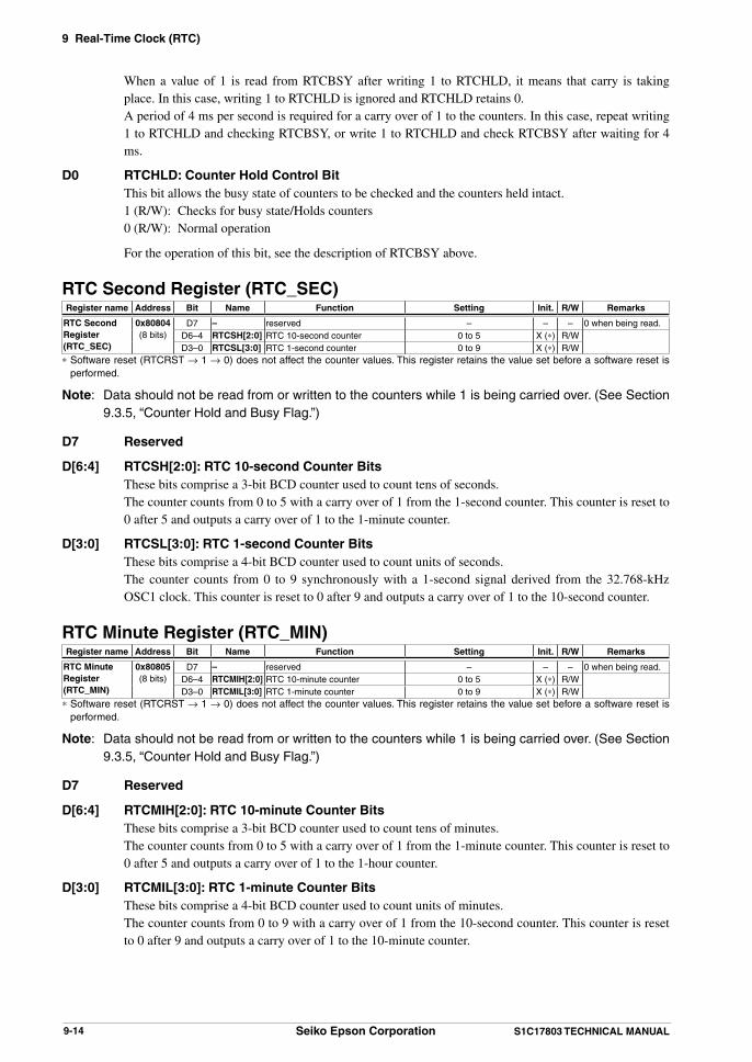
9 Real-Time Clock (RTC)
9-14 Seiko Epson Corporation S1C17803 TECHNICAL MANUAL
When a value of 1 is read from RTCBSY after writing 1 to RTCHLD, it means that carry is taking place. In this case, writing 1 to RTCHLD is ignored and RTCHLD retains 0.
A period of 4 ms per second is required for a carry over of 1 to the counters. In this case, repeat writing 1 to RTCHLD and checking RTCBSY, or write 1 to RTCHLD and check RTCBSY after waiting for 4 ms.
D0 RTCHLD: Counter Hold Control Bit This bit allows the busy state of counters to be checked and the counters held intact. 1 (R/W): Checks for busy state/Holds counters 0 (R/W): Normal operation
For the operation of this bit, see the description of RTCBSY above.
RTC Second Register (RTC_SEC)Register name Address Bit Name Function Setting Init. R/W Remarks
RTC Second Register(RTC_SEC)
0x80804(8 bits)
D7 – reserved – – – 0 when being read.D6–4 RTCSH[2:0] RTC 10-second counter 0 to 5 X (*) R/WD3–0 RTCSL[3:0] RTC 1-second counter 0 to 9 X (*) R/W
* Software reset (RTCRST → 1 → 0) does not affect the counter values. This register retains the value set before a software reset is performed.
Note: Data should not be read from or written to the counters while 1 is being carried over. (See Section 9.3.5, “Counter Hold and Busy Flag.”)
D7 Reserved
D[6:4] RTCSH[2:0]: RTC 10-second Counter Bits These bits comprise a 3-bit BCD counter used to count tens of seconds. The counter counts from 0 to 5 with a carry over of 1 from the 1-second counter. This counter is reset to
0 after 5 and outputs a carry over of 1 to the 1-minute counter.
D[3:0] RTCSL[3:0]: RTC 1-second Counter Bits These bits comprise a 4-bit BCD counter used to count units of seconds. The counter counts from 0 to 9 synchronously with a 1-second signal derived from the 32.768-kHz
OSC1 clock. This counter is reset to 0 after 9 and outputs a carry over of 1 to the 10-second counter.
RTC Minute Register (RTC_MIN)Register name Address Bit Name Function Setting Init. R/W Remarks
RTC Minute Register(RTC_MIN)
0x80805(8 bits)
D7 – reserved – – – 0 when being read.D6–4 RTCMIH[2:0] RTC 10-minute counter 0 to 5 X (*) R/WD3–0 RTCMIL[3:0] RTC 1-minute counter 0 to 9 X (*) R/W
* Software reset (RTCRST → 1 → 0) does not affect the counter values. This register retains the value set before a software reset is performed.
Note: Data should not be read from or written to the counters while 1 is being carried over. (See Section 9.3.5, “Counter Hold and Busy Flag.”)
D7 Reserved
D[6:4] RTCMIH[2:0]: RTC 10-minute Counter Bits These bits comprise a 3-bit BCD counter used to count tens of minutes. The counter counts from 0 to 5 with a carry over of 1 from the 1-minute counter. This counter is reset to
0 after 5 and outputs a carry over of 1 to the 1-hour counter.
D[3:0] RTCMIL[3:0]: RTC 1-minute Counter Bits These bits comprise a 4-bit BCD counter used to count units of minutes. The counter counts from 0 to 9 with a carry over of 1 from the 10-second counter. This counter is reset
to 0 after 9 and outputs a carry over of 1 to the 10-minute counter.

9 Real-Time Clock (RTC)
S1C17803 TECHNICAL MANUAL Seiko Epson Corporation 9-15
RTC Hour Register (RTC_HOUR)Register name Address Bit Name Function Setting Init. R/W Remarks
RTC Hour Register(RTC_HOUR)
0x80806(8 bits)
D7–6 – reserved – – – 0 when being read.D5–4 RTCHH[1:0] RTC 10-hour counter 0 to 2 X (*) R/WD3–0 RTCHL[3:0] RTC 1-hour counter 0–9 X (*) R/W
* Software reset (RTCRST → 1 → 0) does not affect the counter values. This register retains the value set before a software reset is performed.
Notes: • Data should not be read from or written to the counters while 1 is being carried over. (See Section 9.3.5, “Counter Hold and Busy Flag.”)
• Rewriting RTC24H/RTC_CNTL0 register may corrupt the count data in this register. Therefore, after changing the RTC24H setting, be sure to set up this register again.
D[7:6] Reserved
D[5:4] RTCHH[1:0]: RTC 10-hour Counter Bits These bits comprise a 2-bit BCD counter used to count tens of hours. With a carry over of 1 from the 1-hour counter, the counter counts from 0 to 2. The counter is reset at
24 o’clock, and outputs a carry over of 1 to the 1-day counter.
D[3:0] RTCHL[3:0]: RTC 1-hour Counter Bits These bits comprise a 4-bit BCD counter used to count units of hours. The counter counts from 0 to 9 with a carry over of 1 from the 10-minute counter. This counter is reset
to 0 after 9 and outputs a carry over of 1 to the 10-hour counter. The counter is reset at 24 o’clock.
RTC Day Register (RTC_DAY)Register name Address Bit Name Function Setting Init. R/W Remarks
RTC Day Register(RTC_DAY)
0x80807(8 bits)
D7–6 – reserved – – – 0 when being read.D5–4 RTCDH[1:0] RTC 10-day counter 0 to 3 X (*) R/WD3–0 RTCDL[3:0] RTC 1-day counter 0 to 9 X (*) R/W
* Software reset (RTCRST → 1 → 0) does not affect the counter values. This register retains the value set before a software reset is performed.
Notes: • Data should not be read from or written to the counters while 1 is being carried over. (See Section 9.3.5, “Counter Hold and Busy Flag.”)
• Rewriting RTC24H/RTC_CNTL0 register may corrupt the count data in this register. Therefore, after changing the RTC24H setting, be sure to set up this register again.
D[7:6] Reserved
D[5:4] RTCDH[1:0]: RTC 10-day Counter Bits These bits comprise a 2-bit BCD counter used to count tens of days. The counter counts from 0 to 2 or
3 with a carry over of 1 from the 1-day counter. The number of days in each month and leap years are taken into account, so that when months change the counter is reset to 0 along with the 1-day counter, and a carry over of 1 is output to the 1-month counter.
D[3:0] RTCDL[3:0]: RTC 1-day Counter Bits These bits comprise a 4-bit BCD counter used to count units of days. The counter counts from 0 to 9 with a carry over of 1 from the hour counter. This counter is reset to 0
after 9 and outputs a carry over of 1 to the 10-day counter. The number of days in each month and leap years are taken into account, so that the counter is reset to 1 when months change.
RTC Month Register (RTC_MONTH)Register name Address Bit Name Function Setting Init. R/W Remarks
RTC Month Register(RTC_MONTH)
0x80808(8 bits)
D7–5 – reserved – – – 0 when being read.D4 RTCMOH RTC 10-month counter 0 to 1 X (*) R/W
D3–0 RTCMOL[3:0] RTC 1-month counter 0 to 9 X (*) R/W* Software reset (RTCRST → 1 → 0) does not affect the counter values. This register retains the value set before a software reset is
performed.

9 Real-Time Clock (RTC)
9-16 Seiko Epson Corporation S1C17803 TECHNICAL MANUAL
Notes: • Data should not be read from or written to the counters while 1 is being carried over. (See Section 9.3.5, “Counter Hold and Busy Flag.”)
• Rewriting RTC24H/RTC_CNTL0 register may corrupt the count data in this register. Therefore, after changing the RTC24H setting, be sure to set up this register again.
D[7:5] Reserved
D4 RTCMOH: RTC 10-month Counter Bit This is a tens of months count bit. This bit is set to 1 with a carry over of 1 from the 1-month counter. When years change, this bit is reset
to 0 along with the 1-month counter, and a carry over of 1 is output to the 1-year counter.
D[3:0] RTCMOL[3:0]: RTC 1-month Counter Bits These bits comprise a 4-bit BCD counter used to count units of months. The counter counts from 0 to 9 with a carry over of 1 from the day counter. This counter is reset to 0 af-
ter 9 and outputs a carry over of 1 to the 10-month counter. The counter is reset to 1 when years change.
RTC Year Register (RTC_YEAR)Register name Address Bit Name Function Setting Init. R/W Remarks
RTC Year Register(RTC_YEAR)
0x80809(8 bits)
D7–4 RTCYH[3:0] RTC 10-year counter 0 to 9 X (*) R/WD3–0 RTCYL[3:0] RTC 1-year counter 0 to 9 X (*) R/W
* Software reset (RTCRST → 1 → 0) does not affect the counter values. This register retains the value set before a software reset is performed.
Notes: • Data should not be read from or written to the counters while 1 is being carried over. (See Section 9.3.5, “Counter Hold and Busy Flag,” and Section 9.3.6, “Reading from and Writing to Counters in Operation.”)
• Rewriting RTC24H/RTC_CNTL0 register may corrupt the count data in this register. Therefore, after changing the RTC24H setting, be sure to set up this register again.
D[7:4] RTCYH[3:0]: RTC 10-year Counter Bits These bits comprise a 4-bit BCD counter used to count tens of years. The counter counts from 0 to 9
with a carry over of 1 from the 1-year counter.
D[3:0] RTCYL[3:0]: RTC 1-year Counter Bits These bits comprise a 4-bit BCD counter used to count units of years. The counter counts from 0 to 9 with a carry over of 1 from the month counter. This counter is reset to 0
after 9 and outputs a carry over of 1 to the 10-year counter.
RTC Days of Week Register (RTC_WEEK)Register name Address Bit Name Function Setting Init. R/W Remarks
RTC Days of Week Register(RTC_WEEK)
0x8080a(8 bits)
D7–3 – reserved – – – 0 when being read.D2–0 RTCWK[2:0] RTC days of week counter RTCWK[2:0] Days of week X (*) R/W
0x70x60x50x40x30x20x10x0
–Saturday
FridayThursday
WednesdayTuesdayMondaySunday
* Software reset (RTCRST → 1 → 0) does not affect the counter values. This register retains the value set before a software reset is performed.
Notes: • Data should not be read from or written to the counters while 1 is being carried over. (See Section 9.3.5, “Counter Hold and Busy Flag,” and Section 9.3.6, “Reading from and Writing to Counters in Operation.”)
• Rewriting RTC24H/RTC_CNTL0 register may corrupt the count data in this register. Therefore, after changing the RTC24H setting, be sure to set up this register again.

9 Real-Time Clock (RTC)
S1C17803 TECHNICAL MANUAL Seiko Epson Corporation 9-17
D[7:3] Reserved
D[2:0] RTCWK[2:0]: RTC Days of Week Counter Bits This is a septenary counter (that counts from 0 to 6) representing days of the week. This counter counts
at the same timing as the 1-day counter. The correspondence between the counter values and days of the week can be set in a program as de-
sired. Table 9.6.3 lists the basic correspondence.
Table 9.6.3 Correspondence between Counter Values and Days of the WeekRTCWK[2:0] Days of the week
0x6 Saturday0x5 Friday0x4 Thursday0x3 Wednesday0x2 Tuesday0x1 Monday0x0 Sunday
(Default: indeterminate, software reset: previous value retained)
RTC Wakeup Configuration Register (RTC_WAKEUP)Register name Address Bit Name Function Setting Init. R/W Remarks
RTC Wakeup Configuration Register(RTC_WAKEUP)
0x8080f(8 bits)
D7–2 – reserved – – – 0 when being read.
D1 WUP_CTL WAKEUP control 1 Active 0 Inactive X (0) R/WD0 WUP_POL WAKEUP polarity select 1 Active low 0 Active high X (0) R/W
Init.: ( ) indicates the value set after a software reset (RTCRST → 1 → 0) is performed.
D[7:2] Reserved
D1 WUP_CTL: WAKEUP Control Bit This bit controls the WAKEUP output. 1 (R/W): Active 0 (R/W): Inactive
This bit is used to control the WAKEUP output with software. The WAKEUP signal will also be as-serted when a cause of RTC interrupt occurs.
D0 WUP_POL: WAKEUP Polarity Select Bit This bit select the active level of the WAKEUP output signal. 1 (R/W): Active low 0 (R/W): Active high
RTC Wait Control Register (RTC_WAIT)Register name Address Bit Name Function Setting Init. R/W Remarks
RTC Wait Con-trol Register(RTC_WAIT)
0x80910(8 bits)
D7–3 – reserved – – – 0 when being read.D2–0 RTC_WAIT
[2:0]RTC access wait cycle setup RTC_WAIT[2:0] Wait cycle 0x7 R/W
0x7:
0x0
7 cycles:
0 cycles
D[7:3] Reserved
D[2:0] RTC_WAIT[2:0]: RTC Access Wait Cycle Setup Bits These bits set the number of wait cycles to be inserted when an RTC register is accessed.
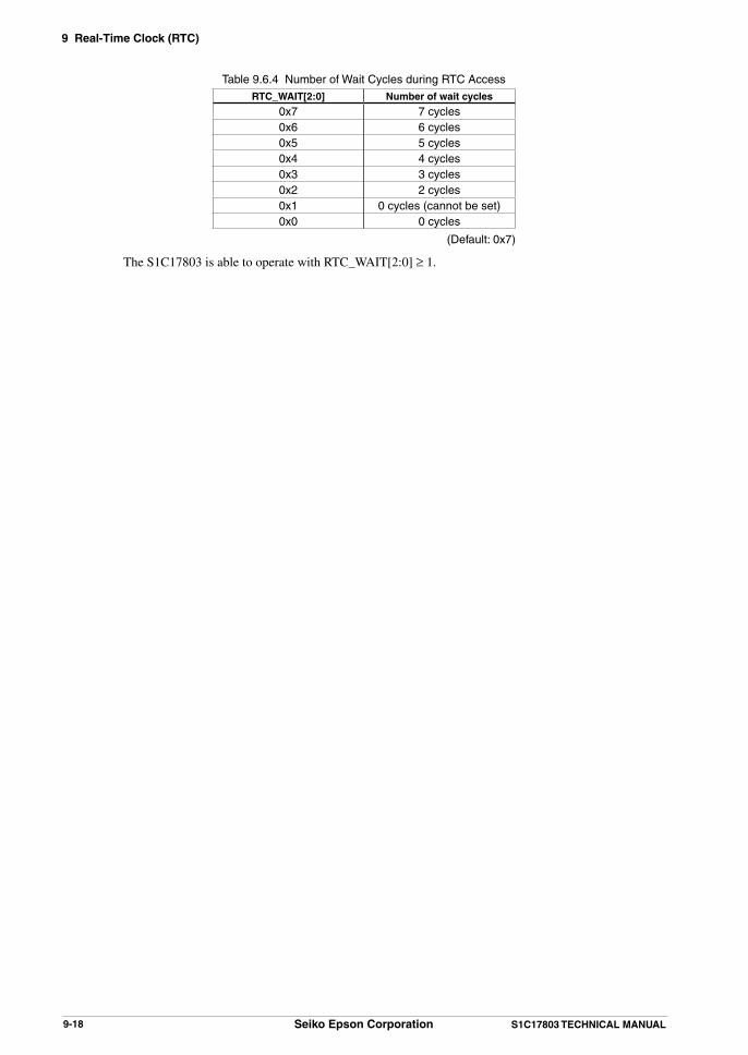
9 Real-Time Clock (RTC)
9-18 Seiko Epson Corporation S1C17803 TECHNICAL MANUAL
Table 9.6.4 Number of Wait Cycles during RTC AccessRTC_WAIT[2:0] Number of wait cycles
0x7 7 cycles0x6 6 cycles0x5 5 cycles0x4 4 cycles0x3 3 cycles0x2 2 cycles0x1 0 cycles (cannot be set)0x0 0 cycles
(Default: 0x7)
The S1C17803 is able to operate with RTC_WAIT[2:0] ≥ 1.

10 Flash Controller (FLASHC)
S1C17803 TECHNICAL MANUAL Seiko Epson Corporation 10-1
10 Flash Controller (FLASHC)
10.1 FLASHC Module OverviewThe S1C17803 incorporates a 128K-byte Flash memory and a FLASHC (Flash Controller) for accessing the Flash memory. In addition to reading from the Flash memory, the FLASHC supports erasing and programming of the Flash memory from the application program.The following shows the main features of the embedded Flash memory and FLASHC.
Flash memoryMemory size 128K bytes (64K × 16 bits)
Sector size 512 words (16 bits) / sector
Erase/program time Chip erase time: 100 ms (typ.) Sector erase time: 20 ms (typ.) Word program time: 15 µs (typ.)
Read access time 50 ns (typ.)
Erase/program interface Write pulse input type
Reliability Endurance: 1000 cycles (min.) Data retention: 10 years (min.)
FLASHCWriting Supports 16-bit writing only.
Reading Supports 8-, 16-, and 32-bit reading. The S1C17 Core can access the Flash memory with no wait cycle (minimum of one access cycle). If the
system clock is faster than the access time, it is necessary to insert a wait cycle (configurable with software).
Notes: • The FLASH_CTL register is write-protected. Before the FLASH_CTL register can be rewrit-ten, its write protection must be removed by writing data 0x96 to the FLS_PROT[7:0]/FLASH_PROT register. Note that since unnecessary rewrites to the FLASH_CTL register could lead to erratic system operation, FLS_PROT[7:0] should be set to other than 0x96 unless the FLASH_CTL register must be rewritten.
• The S1C17 Core accesses the stack for writing in 32-bit unit when calling/returning to/from interrupt handlers or subroutines, therefore, a stack cannot be located in the Flash memory area to which data is always written in 16-bit units.

10 Flash Controller (FLASHC)
10-2 Seiko Epson Corporation S1C17803 TECHNICAL MANUAL
10.2 Flash Memory MapThe Flash memory is located from address 0x8000 to address 0x27fff.
Peripheral area
Peripheral area
SRAMC #CE3–#CE0 areas
IRAM/IVRAM area
Reserved for core I/O area
reserved
reserved
Flash area(128K bytes)
Vector table
reserved
reserved
0xff ffff
0xff fc000xff fbff
0xff 00000xfe ffff
0x10 00000x0f ffff
0x0f c0000x0f bfff
0x08 30000x08 2fff
0x08 00000x07 ffff
0x02 80000x02 7fff
0x00 80000x00 7fff
0x00 60000x00 5fff
0x00 40000x00 3fff
0x00 0000
IRAM/IVRAM mirror area
Figure 10.2.1 Flash Memory Map
After an initial reset, the vector table is located at the beginning of the Flash memory (address 0x8000). Therefore, the boot vector must be written to address 0x8000. For more information on the vector table, see the “Interrupt Controller (ITC)” chapter.
10.3 Programming the Flash MemoryThis section explains how to erase and program the Flash memory.
Precautions on Flash programming(1) The FLASH_CTL register is write-protected. Before the FLASH_CTL register can be rewritten, its write
protection must be removed by writing data 0x96 to the FLS_PROT[7:0]/FLASH_PROT register. Note that since unnecessary rewrites to the FLASH_CTL register could lead to erratic system operation, FLS_PROT[7:0] should be set to other than 0x96 unless the FLASH_CTL register must be rewritten.
(2) Disable the watchdog timer reset function before starting Flash erase/program operations.
(3) Disable interrupts before starting Flash erase/program operations.
(4) Be sure to fix the #RESET pin at high (inactive) during erasing/programming the Flash memory.
(5) Use the internal RAM or external ROM to store and execute the instructions for erasing/programming the Flash memory.
(6) Make sure that the Flash memory is not busy by reading a FLASHC status flag before starting Flash erase/program operations.

10 Flash Controller (FLASHC)
S1C17803 TECHNICAL MANUAL Seiko Epson Corporation 10-3
(7) The FLASHC supports only 16-bit writing for programming the Flash memory. The FLASHC will do noth-ing if an attempt is made to write data to Flash memory in an 8-bit, 24-bit, or 32-bit write instruction.
(8) The S1C17 Core accesses the stack for writing in 32-bit unit when calling/returning to/from interrupt han-dlers or subroutines, therefore, a stack cannot be located in the Flash memory area to which data is always written in 16-bit units.
(9) Both the minimum and maximum values of each erase/program cycle parameter listed in the table below must be guaranteed with software.
Table 10.3.1 Erase/Program Cycle Timing Parameters
ParameterTiming specs
Min. Typ. Max.
Chip erase operation mode hold time 12 µs – –Sector erase operation mode hold time 6 µs – –Program operation mode hold time 4 µs – –Chip erase pulse width 70 ms 100 ms 500 msSector erase pulse width 15 ms 20 ms 50 msProgram pulse width 10 µs 15 µs 20 µs
10.3.1 Chip Erase Procedure
The following shows a chip erase procedure:
Start
End
Disable write protection
Flash busy?
yes
no
Flash busy?
yes
no
(1)
Flash busy?
no
yes
(4)
(9)
(2)
Wait 100 ms
Error handling
(5)
Start hold time(6)
Wait at least 12 µs(7)
Stop erasing(8)
Disable erase mode(10)
Enable write protection(11)
Enable chip erase modeStart erasing
(3)
Figure 10.3.1.1 Chip Erase Flow
(1) Read FLS_STAT/FLASH_CTL register to check whether the Flash memory is in busy status or not. If FLS_STAT is 0, the Flash memory is ready to erase. Go to Step (2). If FLS_STAT is 1, the Flash memory is in busy status such as during reading, erasing, programming, or hard-
ware reset status. In this case, wait until FLS_STAT goes 0.
(2) Write 0x96 to FLS_PROT[7:0]/FLASH_PROT register to remove write protection of the FLASH_CTL register.

10 Flash Controller (FLASHC)
10-4 Seiko Epson Corporation S1C17803 TECHNICAL MANUAL
(3) Write 0x104 to the FLASH_CTL register. This sets CHIP_ERS_EN/FLASH_CTL register to 1 to enable chip erase mode and sets START_ERASE/FLASH_CTL register to 1 to start chip erase operation.
(4) Read FLS_STAT to check whether the Flash memory is in busy status or not. When the FLASHC starts erasing, FLS_STAT goes 1. Go to Step (5). If FLS_STAT is 0, the FLASHC could not start erasing. It may caused by enabling both chip and sector erase
modes at the same time or by occurrence of an error in the system. Execute an error recovery routine and go to Step (10).
(5) Wait for 100 ms to generate an appropriate chip erase pulse width.
(6) Write 0x204 to the FLASH_CTL register. This sets START_HOLD/FLASH_CTL register to 1 to start the chip erase operation mode hold period (the #CE signal for the Flash memory becomes inactive). At this time, keep CHIP_ERS_EN/FLASH_CTL register to 1 to continue chip erase mode.
(7) Wait at least 12 µs to generate the chip erase operation mode hold time.
(8) Write 0x404 to the FLASH_CTL register. This sets STOP/FLASH_CTL register to 1 to finish chip erasing.
(9) Read FLS_STAT to check whether the Flash memory is in busy status or not. If FLS_STAT is 0, the chip erase operation has finished normally. Go to Step (10). If FLS_STAT is 1, an error has occurred during erasing. Execute an error recovery routine and go to Step (10).
(10) Write 0x0 to the FLASH_CTL register. This resets CHIP_ERS_EN/FLASH_CTL register to 0 to disable chip erase mode.
(11) Write a value other than 0x96 to FLS_PROT[7:0] to enable write protection of the FLASH_CTL register.
10.3.2 Sector Erase Procedure
The following shows a sector erase procedure:
Start
End
Disable write protection
Set sector address
Flash busy?
yes
no
Flash busy?
yes
no
(2)
(1)
Flash busy?
no
yes
(5)
(10)
(3)
Wait 20 ms
Error handling
(6)
Start hold time(7)
Wait at least 6 µs(8)
Stop erasing(9)
Disable sector erase mode(11)
Enable write protection(12)
Enable sector erase modeStart erasing
(4)
Figure 10.3.2.1 Sector Erase Flow

10 Flash Controller (FLASHC)
S1C17803 TECHNICAL MANUAL Seiko Epson Corporation 10-5
(1) Set the sector address to be erased to FLS_ADDR[6:0]/FLASH_ADDR register. Flash memory address[16:10] (S1C17803 address 0x8000 = Flash memory address 0x0) should be set to this
register as the sector address.
Table 10.3.2.1 Corresponding Between Memory Address and Flash SectorMemoryaddress
Sector address
Memory address
Sector address
Memory address
Sector address
Memory address
Sector address
0x8000–0x83ff 0x0 0x10000–0x103ff 0x20 0x18000–0x183ff 0x40 0x20000–0x203ff 0x600x8400–0x87ff 0x1 0x10400–0x107ff 0x21 0x18400–0x187ff 0x41 0x20400–0x207ff 0x610x8800–0x8bff 0x2 0x10800–0x10bff 0x22 0x18800–0x18bff 0x42 0x20800–0x20bff 0x620x8c00–0x8fff 0x3 0x10c00–0x10fff 0x23 0x18c00–0x18fff 0x43 0x20c00–0x20fff 0x630x9000–0x93ff 0x4 0x11000–0x113ff 0x24 0x19000–0x193ff 0x44 0x21000–0x213ff 0x640x9400–0x97ff 0x5 0x11400–0x117ff 0x25 0x19400–0x197ff 0x45 0x21400–0x217ff 0x650x9800–0x9bff 0x6 0x11800–0x11bff 0x26 0x19800–0x19bff 0x46 0x21800–0x21bff 0x660x9c00–0x9fff 0x7 0x11c00–0x11fff 0x27 0x19c00–0x19fff 0x47 0x21c00–0x21fff 0x670xa000–0xa3ff 0x8 0x12000–0x123ff 0x28 0x1a000–0x1a3ff 0x48 0x22000–0x223ff 0x680xa400–0xa7ff 0x9 0x12400–0x127ff 0x29 0x1a400–0x1a7ff 0x49 0x22400–0x227ff 0x690xa800–0xabff 0xa 0x12800–0x12bff 0x2a 0x1a800–0x1abff 0x4a 0x22800–0x22bff 0x6a0xac00–0xafff 0xb 0x12c00–0x12fff 0x2b 0x1ac00–0x1afff 0x4b 0x22c00–0x22fff 0x6b0xb000–0xb3ff 0xc 0x13000–0x133ff 0x2c 0x1b000–0x1b3ff 0x4c 0x23000–0x233ff 0x6c0xb400–0xb7ff 0xd 0x13400–0x137ff 0x2d 0x1b400–0x1b7ff 0x4d 0x23400–0x237ff 0x6d0xb800–0xbbff 0xe 0x13800–0x13bff 0x2e 0x1b800–0x1bbff 0x4e 0x23800–0x23bff 0x6e0xbc00–0xbfff 0xf 0x13c00–0x13fff 0x2f 0x1bc00–0x1bfff 0x4f 0x23c00–0x23fff 0x6f0xc000–0xc3ff 0x10 0x14000–0x143ff 0x30 0x1c000–0x1c3ff 0x50 0x24000–0x243ff 0x700xc400–0xc7ff 0x11 0x14400–0x147ff 0x31 0x1c400–0x1c7ff 0x51 0x24400–0x247ff 0x710xc800–0xcbff 0x12 0x14800–0x14bff 0x32 0x1c800–0x1cbff 0x52 0x24800–0x24bff 0x720xcc00–0xcfff 0x13 0x14c00–0x14fff 0x33 0x1cc00–0x1cfff 0x53 0x24c00–0x24fff 0x730xd000–0xd3ff 0x14 0x15000–0x153ff 0x34 0x1d000–0x1d3ff 0x54 0x25000–0x253ff 0x740xd400–0xd7ff 0x15 0x15400–0x157ff 0x35 0x1d400–0x1d7ff 0x55 0x25400–0x257ff 0x750xd800–0xdbff 0x16 0x15800–0x15bff 0x36 0x1d800–0x1dbff 0x56 0x25800–0x25bff 0x760xdc00–0xdfff 0x17 0x15c00–0x15fff 0x37 0x1dc00–0x1dfff 0x57 0x25c00–0x25fff 0x770xe000–0xe3ff 0x18 0x16000–0x163ff 0x38 0x1e000–0x1e3ff 0x58 0x26000–0x263ff 0x780xe400–0xe7ff 0x19 0x16400–0x167ff 0x39 0x1e400–0x1e7ff 0x59 0x26400–0x267ff 0x790xe800–0xebff 0x1a 0x16800–0x16bff 0x3a 0x1e800–0x1ebff 0x5a 0x26800–0x26bff 0x7a0xec00–0xefff 0x1b 0x16c00–0x16fff 0x3b 0x1ec00–0x1efff 0x5b 0x26c00–0x26fff 0x7b0xf000–0xf3ff 0x1c 0x17000–0x173ff 0x3c 0x1f000–0x1f3ff 0x5c 0x27000–0x273ff 0x7c0xf400–0xf7ff 0x1d 0x17400–0x177ff 0x3d 0x1f400–0x1f7ff 0x5d 0x27400–0x277ff 0x7d0xf800–0xfbff 0x1e 0x17800–0x17bff 0x3e 0x1f800–0x1fbff 0x5e 0x27800–0x27bff 0x7e0xfc00–0xffff 0x1f 0x17c00–0x17fff 0x3f 0x1fc00–0x1ffff 0x5f 0x27c00–0x27fff 0x7f
(2) Read FLS_STAT/FLASH_CTL register to check whether the Flash memory is in busy status or not. If FLS_STAT is 0, the Flash memory is ready to erase. Go to Step (3). If FLS_STAT is 1, the Flash memory is in busy status such as during reading, erasing, programming, or hard-
ware reset status. In this case, wait until FLS_STAT goes 0.
(3) Write 0x96 to FLS_PROT[7:0]/FLASH_PROT to remove write protection of the FLASH_CTL register.
(4) Write 0x102 to the FLASH_CTL register. This sets SCT_ERS_EN/FLASH_CTL register to 1 to enable sector erase mode and sets START_ERASE/FLASH_CTL register to 1 to start sector erase operation.
(5) Read FLS_STAT to check whether the Flash memory is in busy status or not. When the FLASHC starts erasing, FLS_STAT goes 1. Go to Step (6). If FLS_STAT is 0, the FLASHC could not start erasing. It may caused by enabling both chip and sector erase
modes at the same time or by occurrence of an error in the system. Execute an error recovery routine and go to Step (11).
(6) Wait for 20 ms to generate an appropriate sector erase pulse width.
(7) Write 0x202 to the FLASH_CTL register. This sets START_HOLD/FLASH_CTL register to 1 to start the sec-tor erase operation mode hold period (the #CE signal for the Flash memory becomes inactive). At this time, keep SCT_ERS_EN/FLASH_CTL register to 1 to continue sector erase mode.
(8) Wait at least 6 µs to generate the sector erase operation mode hold time.

10 Flash Controller (FLASHC)
10-6 Seiko Epson Corporation S1C17803 TECHNICAL MANUAL
(9) Write 0x402 to the FLASH_CTL register. This sets STOP/FLASH_CTL register to 1 to finish sector erasing.
(10) Read FLS_STAT to check whether the Flash memory is in busy status or not. If FLS_STAT is 0, the sector erase operation has finished normally. Go to Step (11). If FLS_STAT is 1, an error has occurred during erasing. Execute an error recovery routine and go to Step (11).
(11) Write 0x0 to the FLASH_CTL register. This resets SCT_ERS_EN/FLASH_CTL register to 0 to disable sector erase mode.
(12) Write a value other than 0x96 to FLS_PROT[7:0] to enable write protection of the FLASH_CTL register.
10.3.3 Flash Programming Procedure
The following shows a Flash programming (writing) procedure:
Start
End
Disable write protection
Flash busy?
yes
no
Flash busy?
yes
no
(1)
Flash busy?
no
yes
(5)
(10)
(2)
Write 16-bit data(4)
Wait 15 µs
Error handling
(6)
Start hold time(7)
Wait at least 4 µs(8)
Stop Flash programming(9)
Disable Flash programming mode
(11)
Enable write protection(12)
Enable Flash programming mode
(3)
Figure 10.3.3.1 Flash Programming Flow
(1) Read FLS_STAT/FLASH_CTL register to check whether the Flash memory is in busy status or not. If FLS_STAT is 0, the Flash memory is ready to program. Go to Step (2). If FLS_STAT is 1, the Flash memory is in busy status such as during reading, erasing, programming, or hard-
ware reset status. In this case, wait until FLS_STAT goes 0.
(2) Write 0x96 to FLS_PROT[7:0]/FLASH_PROT to remove write protection of the FLASH_CTL register.
(3) Write 0x1 to the FLASH_CTL register. This sets WR_EN/FLASH_CTL register to 1 to enable Flash program-ming mode.
(4) Write 16-bit data using a 16-bit data transfer instruction. Do not to use an 8-bit, 24-bit, or 32-bit data transfer instruction.

10 Flash Controller (FLASHC)
S1C17803 TECHNICAL MANUAL Seiko Epson Corporation 10-7
(5) Read FLS_STAT to check whether the Flash memory is in busy status or not. When the FLASHC starts programming, FLS_STAT goes 1. Go to Step (6). If FLS_STAT is 0, the FLASHC could not start programming. It may caused by an error in the system. Execute
an error recovery routine and go to Step (11).
(6) Wait for 15 µs to generate an appropriate Flash program pulse width.
(7) Write 0x201 to the FLASH_CTL register. This sets START_HOLD/FLASH_CTL register to 1 to start the pro-gram operation mode hold period (the #CE signal for the Flash memory becomes inactive). At this time, keep WR_EN/FLASH_CTL register to 1 to continue Flash programming mode.
(8) Wait at least 4 µs to generate the program operation mode hold time.
(9) Write 0x401 to the FLASH_CTL register. This sets STOP/FLASH_CTL register to 1 to finish Flash program-ming.
(10) Read FLS_STAT to check whether the Flash memory is in busy status or not. If FLS_STAT is 0, the Flash programming operation has finished normally. Go to Step (11). If FLS_STAT is 1, an error has occurred during programming. Execute an error recovery routine and go to Step
(11).
(11) Write 0x0 to the FLASH_CTL register. This resets WR_EN/FLASH_CTL register to 0 to disable Flash pro-gramming mode.
(12) Write a value other than 0x96 to FLS_PROT[7:0] to enable write protection of the FLASH_CTL register.
10.4 Read Access Control In order to read data from the Flash memory properly even if the system operates with a high-speed clock, the FLASHC can insert a wait cycle in the Flash read cycle. The number of system clock cycles to be inserted as a wait cycle can be specified using FLS_WAIT[2:0]/FLASH_WAIT register. Set the appropriate number of cycles accord-ing to the system clock frequency.
Table 10.4.1 Setting Read Access Wait CycleFLS_WAIT[2:0] Number of wait cycles Number of read access cycles System clock frequency
0x7 7 cycles 8 cycles 33 MHz or less0x6 6 cycles 7 cycles0x5 5 cycles 6 cycles0x4 4 cycles 5 cycles0x3 3 cycles 4 cycles0x2 2 cycles 3 cycles0x1 1 cycle 2 cycles0x0 0 cycles 1 cycle 16 MHz or less
(Default: 0x7)
Note: The variation of the Flash read access cycles with the different FLS_WAIT[2:0] settings cannot be monitored from outside the IC as the FLASHC includes a Flash memory pre-fetch circuit. There-fore, be sure to avoid setting of FLS_WAIT[2:0] to a value that is not supported in the system clock frequency.
10.5 HIDE modeBy default the S1C17803 FLASHC is placed into HIDE mode that disables reading data from the 16K-byte area at the end of the Flash memory (addresses 0x24000 to 0x27fff). However, the S1C17 Core is able to fetch instructions from this area as well as programming (writing to) this area.The HIDE mode can be used as a simple read-protection mechanism by placing the code to be hidden in this area. In HIDE mode, 0xffff (in 16-bit read) is always read out from this area.To read data from this area, the HIDE mode must be canceled. Instruction literature for canceling/setting HIDE mode is available from the Epson MCU Users’ Site.

10 Flash Controller (FLASHC)
10-8 Seiko Epson Corporation S1C17803 TECHNICAL MANUAL
Notes: • The HIDE mode cancelling procedure is only released to developers whose product actually incorporates the S1C17803. However, Seiko Epson cannot guarantee confidentiality.
• Data such as constants should not be placed in this protected area, as the application re-quires canceling HIDE mode before reading.
• After the Flash memory is programmed using the debugger, set the FLASHC to HIDE mode before starting debugging to match the same usage condition as the actual product. The FLASHC can also be placed into HIDE mode by an initial reset or enabling write-protection for the FLASHC registers.
10.6 Control Register Details
Table 10.6.1 List of FLASHC RegistersAddress Register name Function0x81700 FLASH_CTL FLASHC Control Register Controls Flash erase/program operations.0x81702 FLASH_ADDR FLASHC Sector Address Register Sets the Flash address for erasing a sector.0x81704 FLASH_WAIT FLASHC Wait Register Sets the wait cycle for Flash read.0x81710 FLASH_PROT FLASHC Protect Register Enables Flash control registers for writing.
The following describes each FLASHC control register. These are all 16-bit registers.
Note: When setting the registers, be sure to write 0, and not 1, for all “reserved bits.”
FLASHC Control Register (FLASH_CTL)Register name Address Bit Name Function Setting Init. R/W Remarks
FLASHCControl Register(FLASH_CTL)
0x81700(16 bits)
D15 FLS_STAT Flash status flag 1 Busy 0 Idle 1 RD14–11 – reserved – – – 0 when being read.
D10 STOP Flash erase/program stop 1 Stop 0 Ignored 0 W 0 when being read.Write-protectedD9 START
_HOLDHold period start 1 Start 0 Ignored 0 W
D8 START_ERASE
Flash erasing start 1 Start 0 Ignored 0 W
D7–3 – reserved – – – 0 when being read.D2 CHIP_ERS
_ENFlash chip erase enable 1 Enable 0 Disable 0 R/W Write-protected
D1 SCT_ERS_EN
Flash sector erase enable 1 Enable 0 Disable 0 R/W
D0 WR_EN Flash programming enable 1 Enable 0 Disable 0 R/W
Note: The FLASH_CTL register is write-protected. Before the FLASH_CTL register can be rewritten, its write protection must be removed by writing data 0x96 to the FLS_PROT[7:0]/FLASH_PROT reg-ister. Note that since unnecessary rewrites to the FLASH_CTL register could lead to erratic sys-tem operation, FLS_PROT[7:0] should be set to other than 0x96 unless the FLASH_CTL register must be rewritten.
D15 FLS_STAT: Flash Status Flag Bit Indicates whether the Flash memory is idle or in busy status. 1 (R): Busy (default) 0 (R): Idle 1/0 (W): Has no effect
This flag is set to 1 while the Flash memory is being read, erased, programmed, or the hardware reset sequence is in progress.
Before the Flash memory can be erased or programmed, this flag must be 0. To place the Flash memory in Idle state, the CPU must run with the instructions stored in a memory other than Flash (e.g. internal RAM or external ROM).
D[14:11] Reserved

10 Flash Controller (FLASHC)
S1C17803 TECHNICAL MANUAL Seiko Epson Corporation 10-9
D10 STOP: Flash Erase/Program Stop Bit Stops chip erase, sector erase, or Flash programming operation. 1 (W): Stop 0 (W): Has no effect 0 (R): Always 0 when read (default)
Writing 1 to STOP terminates the chip erase, sector erase, or program operation. This bit should be set to 1 when the operation mode hold time has elapsed after setting START_HOLD to 1.
This bit must be fixed at 0 while the Flash memory is being read.
D9 START_HOLD: Hold Period Start Bit Starts the operation mode hold period. 1 (W): Start 0 (W): Has no effect 0 (R): Always 0 when read (default)
Write 1 to START_HOLD when the chip erase, sector erase, or program time (see Table 10.5.2) has elapsed after setting 1 to START_ERASE or writing data to the Flash memory.
Writing 1 to START_HOLD starts the operation mode hold period by setting the #CE signal for the Flash memory inactive. After that, wait for operation mode hold time (see Table 10.5.2) before termi-nating chip erase, sector erase, or program mode.
This bit must be fixed at 0 while the Flash memory is being read.
Table 10.6.2 Erase/Program Cycle Timing Parameters
ParameterTiming specs
Min. Typ. Max.Chip erase operation mode hold time 12 µs – –Sector erase operation mode hold time 6 µs – –Program operation mode hold time 4 µs – –Chip erase pulse width 70 ms 100 ms 500 msSector erase pulse width 15 ms 20 ms 50 msProgram pulse width 10 µs 15 µs 20 µs
D8 START_ERASE: Flash Erasing Start Bit Starts chip erase or sector erase operation. 1 (W): Start 0 (W): Has no effect 0 (R): Always 0 when read (default)
When performing chip erasing, set CHIP_ERS_EN and START_ERASE to 1. When performing sector erasing, set SCT_ERS_EN and START_ERASE to 1 after setting the sector
address to be erased to the FLS_ADDR[6:0]/FLASH_ADDR register. If CHIP_ERS_EN and SCT_ERS_EN are both set to 0 or 1, writing 1 to START_ERASE is ignored
and it does not start erasing. Do not set this bit to 1 when the Flash memory is in busy status (FLS_STAT = 1).
D[7:3] Reserved
D2 CHIP_ERS_EN: Flash Chip Erase Enable Bit Enables chip erase mode. 1 (R/W): Enable 0 (R/W): Disable (default)
Set CHIP_ERS_EN and START_ERASE to 1 to start chip erasing. After the chip erase operation is ter-minated by setting STOP to 1, reset CHIP_ERS_EN to 0. See Section 10.3.1, “Chip Erase Procedure,” for controlling chip erase operation.
D1 SCT_ERS_EN: Flash Sector Erase Enable Bit Enables sector erase mode. 1 (R/W): Enable 0 (R/W): Disable (default)

10 Flash Controller (FLASHC)
10-10 Seiko Epson Corporation S1C17803 TECHNICAL MANUAL
Set SCT_ERS_EN and START_ERASE (D8) to 1 to start sector erasing after setting the sector address to be erased to the FLASHC Sector Address Register (0x5802). After the sector erase operation is ter-minated by setting STOP (D10) to 1, reset SCT_ERS_EN to 0. See Section 10.3.2, “Sector Erase Pro-cedure,” for controlling sector erase operation.
D0 WR_EN: Flash Programming Enable Bit Enables Flash programming mode. 1 (R/W): Enable 0 (R/W): Disable (default)
Set WR_EN to 1 to start Flash programming mode. After that write data using a 16-bit data transfer in-struction. After the Flash programming operation is terminated by setting STOP to 1, reset WR_EN to 0. See Section 10.3.3, “Flash Programming Procedure,” for controlling Flash programming operation.
FLASHC Sector Address Register (FLASH_ADDR)Register name Address Bit Name Function Setting Init. R/W Remarks
FLASHC Sector Address Register(FLASH_ADDR)
0x81702(16 bits)
D15–7 – reserved – – – 0 when being read.D6–0 FLS_ADDR
[6:0]Erase sector address Address[16:10] 0x0 R/W
D[15:7] ReservedD[6:0] FLS_ADDR[6:0]: Erase Sector Address Bits Specifies the sector to be erased. (Default: 0x0) Specify bit 16 to bit 10 of the Flash memory address (S1C17803 address 0x8000 = Flash memory ad-
dress 0x0) as the sector address.
Table 10.6.3 Corresponding Between Memory Address and Flash SectorMemoryaddress
Sector address
Memory address
Sector address
Memory address
Sector address
Memory address
Sector address
0x8000–0x83ff 0x0 0x10000–0x103ff 0x20 0x18000–0x183ff 0x40 0x20000–0x203ff 0x600x8400–0x87ff 0x1 0x10400–0x107ff 0x21 0x18400–0x187ff 0x41 0x20400–0x207ff 0x610x8800–0x8bff 0x2 0x10800–0x10bff 0x22 0x18800–0x18bff 0x42 0x20800–0x20bff 0x620x8c00–0x8fff 0x3 0x10c00–0x10fff 0x23 0x18c00–0x18fff 0x43 0x20c00–0x20fff 0x630x9000–0x93ff 0x4 0x11000–0x113ff 0x24 0x19000–0x193ff 0x44 0x21000–0x213ff 0x640x9400–0x97ff 0x5 0x11400–0x117ff 0x25 0x19400–0x197ff 0x45 0x21400–0x217ff 0x650x9800–0x9bff 0x6 0x11800–0x11bff 0x26 0x19800–0x19bff 0x46 0x21800–0x21bff 0x660x9c00–0x9fff 0x7 0x11c00–0x11fff 0x27 0x19c00–0x19fff 0x47 0x21c00–0x21fff 0x670xa000–0xa3ff 0x8 0x12000–0x123ff 0x28 0x1a000–0x1a3ff 0x48 0x22000–0x223ff 0x680xa400–0xa7ff 0x9 0x12400–0x127ff 0x29 0x1a400–0x1a7ff 0x49 0x22400–0x227ff 0x690xa800–0xabff 0xa 0x12800–0x12bff 0x2a 0x1a800–0x1abff 0x4a 0x22800–0x22bff 0x6a0xac00–0xafff 0xb 0x12c00–0x12fff 0x2b 0x1ac00–0x1afff 0x4b 0x22c00–0x22fff 0x6b0xb000–0xb3ff 0xc 0x13000–0x133ff 0x2c 0x1b000–0x1b3ff 0x4c 0x23000–0x233ff 0x6c0xb400–0xb7ff 0xd 0x13400–0x137ff 0x2d 0x1b400–0x1b7ff 0x4d 0x23400–0x237ff 0x6d0xb800–0xbbff 0xe 0x13800–0x13bff 0x2e 0x1b800–0x1bbff 0x4e 0x23800–0x23bff 0x6e0xbc00–0xbfff 0xf 0x13c00–0x13fff 0x2f 0x1bc00–0x1bfff 0x4f 0x23c00–0x23fff 0x6f0xc000–0xc3ff 0x10 0x14000–0x143ff 0x30 0x1c000–0x1c3ff 0x50 0x24000–0x243ff 0x700xc400–0xc7ff 0x11 0x14400–0x147ff 0x31 0x1c400–0x1c7ff 0x51 0x24400–0x247ff 0x710xc800–0xcbff 0x12 0x14800–0x14bff 0x32 0x1c800–0x1cbff 0x52 0x24800–0x24bff 0x720xcc00–0xcfff 0x13 0x14c00–0x14fff 0x33 0x1cc00–0x1cfff 0x53 0x24c00–0x24fff 0x730xd000–0xd3ff 0x14 0x15000–0x153ff 0x34 0x1d000–0x1d3ff 0x54 0x25000–0x253ff 0x740xd400–0xd7ff 0x15 0x15400–0x157ff 0x35 0x1d400–0x1d7ff 0x55 0x25400–0x257ff 0x750xd800–0xdbff 0x16 0x15800–0x15bff 0x36 0x1d800–0x1dbff 0x56 0x25800–0x25bff 0x760xdc00–0xdfff 0x17 0x15c00–0x15fff 0x37 0x1dc00–0x1dfff 0x57 0x25c00–0x25fff 0x770xe000–0xe3ff 0x18 0x16000–0x163ff 0x38 0x1e000–0x1e3ff 0x58 0x26000–0x263ff 0x780xe400–0xe7ff 0x19 0x16400–0x167ff 0x39 0x1e400–0x1e7ff 0x59 0x26400–0x267ff 0x790xe800–0xebff 0x1a 0x16800–0x16bff 0x3a 0x1e800–0x1ebff 0x5a 0x26800–0x26bff 0x7a0xec00–0xefff 0x1b 0x16c00–0x16fff 0x3b 0x1ec00–0x1efff 0x5b 0x26c00–0x26fff 0x7b0xf000–0xf3ff 0x1c 0x17000–0x173ff 0x3c 0x1f000–0x1f3ff 0x5c 0x27000–0x273ff 0x7c0xf400–0xf7ff 0x1d 0x17400–0x177ff 0x3d 0x1f400–0x1f7ff 0x5d 0x27400–0x277ff 0x7d0xf800–0xfbff 0x1e 0x17800–0x17bff 0x3e 0x1f800–0x1fbff 0x5e 0x27800–0x27bff 0x7e0xfc00–0xffff 0x1f 0x17c00–0x17fff 0x3f 0x1fc00–0x1ffff 0x5f 0x27c00–0x27fff 0x7f
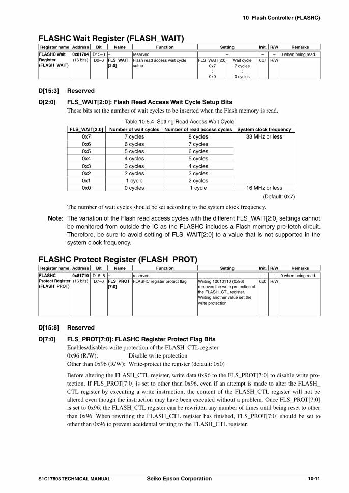
10 Flash Controller (FLASHC)
S1C17803 TECHNICAL MANUAL Seiko Epson Corporation 10-11
FLASHC Wait Register (FLASH_WAIT)Register name Address Bit Name Function Setting Init. R/W Remarks
FLASHC Wait Register(FLASH_WAIT)
0x81704(16 bits)
D15–3 – reserved – – – 0 when being read.D2–0 FLS_WAIT
[2:0]Flash read access wait cycle setup
FLS_WAIT[2:0] Wait cycle 0x7 R/W0x7
:0x0
7 cycles:
0 cycles
D[15:3] Reserved
D[2:0] FLS_WAIT[2:0]: Flash Read Access Wait Cycle Setup Bits These bits set the number of wait cycles to be inserted when the Flash memory is read.
Table 10.6.4 Setting Read Access Wait CycleFLS_WAIT[2:0] Number of wait cycles Number of read access cycles System clock frequency
0x7 7 cycles 8 cycles 33 MHz or less0x6 6 cycles 7 cycles0x5 5 cycles 6 cycles0x4 4 cycles 5 cycles0x3 3 cycles 4 cycles0x2 2 cycles 3 cycles0x1 1 cycle 2 cycles0x0 0 cycles 1 cycle 16 MHz or less
(Default: 0x7)
The number of wait cycles should be set according to the system clock frequency.
Note: The variation of the Flash read access cycles with the different FLS_WAIT[2:0] settings cannot be monitored from outside the IC as the FLASHC includes a Flash memory pre-fetch circuit. Therefore, be sure to avoid setting of FLS_WAIT[2:0] to a value that is not supported in the system clock frequency.
FLASHC Protect Register (FLASH_PROT)Register name Address Bit Name Function Setting Init. R/W Remarks
FLASHCProtect Register(FLASH_PROT)
0x81710(16 bits)
D15–8 – reserved – – – 0 when being read.D7–0 FLS_PROT
[7:0]FLASHC register protect flag Writing 10010110 (0x96)
removes the write protection of the FLASH_CTL register.Writing another value set the write protection.
0x0 R/W
D[15:8] Reserved
D[7:0] FLS_PROT[7:0]: FLASHC Register Protect Flag Bits Enables/disables write protection of the FLASH_CTL register. 0x96 (R/W): Disable write protection Other than 0x96 (R/W): Write-protect the register (default: 0x0)
Before altering the FLASH_CTL register, write data 0x96 to the FLS_PROT[7:0] to disable write pro-tection. If FLS_PROT[7:0] is set to other than 0x96, even if an attempt is made to alter the FLASH_CTL register by executing a write instruction, the content of the FLASH_CTL register will not be altered even though the instruction may have been executed without a problem. Once FLS_PROT[7:0] is set to 0x96, the FLASH_CTL register can be rewritten any number of times until being reset to other than 0x96. When rewriting the FLASH_CTL register has finished, FLS_PROT[7:0] should be set to other than 0x96 to prevent accidental writing to the FLASH_CTL register.

11 SRAM Controller (SRAMC)
S1C17803 TECHNICAL MANUAL Seiko Epson Corporation 11-1
11 SRAM Controller (SRAMC)
11.1 SRAMC Module OverviewThe SRAM controller (SRAMC) is a bus controller module that provides an external bus interface for accessing external devices. The SRAMC functions and features are outlined below.
• 23-bit address bus and 16-bit data bus.
• Outputs four chip-enable signals (#CE0 to #CE3) for external devices.
• Supports two access types for each #CE area: A0 and BSL.
• Supports two device size for each #CE area: 8 bits and 16 bits.
• Supports static wait cycle insertion (0 to 15 cycles, software selectable) for each #CE area.
• Supports burst read function for each #CE area.
• Allows SRAM, ROM, or Flash memory to be connected directly to the external bus.
• Allows wait states to be inserted from the external #WAIT pin (for SRAM type only).
• Little endian (fixed)
• 1 setup cycle and 1 hold cycle (fixed)
• 4 clocks selectable for #CE1: BCLK/1, BCLK/2, BCLK/4, and BCLK/8
11.2 SRAMC PinsTable 11.2.1 lists the pins used by the SRAMC.
Table 11.2.1 SRAMC Pin ListPin name I/O Function
D[15:0] I/O External data bus D[15:0]A0/#BSL O External address bus A0 / Bus strobe (low byte) signal outputA[22:1] O External address bus A[22:1]#CE[3:0] O Chip enable signal outputs#RD O Read signal output#WRL O Write (low byte) signal output#WRH/#BSH O Write (high byte) signal / Bus strobe (high byte) signal output
Note: The external bus control pins above are shared with general-purpose I/O ports and they are configured for I/O ports at initial reset. Before the SRAMC signals assigned to these pins can be used, the functions of these pins must be switched for the SRAMC by setting each corresponding port function select bit.
For details on how to switch over the pin functions, see the “I/O Ports (GPIO)” chapter.
11.3 SRAMC Operating ClockThe SRAMC operates with BCLK supplied from the CMU. BCLK does not stop in normal mode and in HALT mode by default. It can be stopped in HALT mode using a CMU control register. BCLK can also be output to exter-nal devices from the CMU_CLK pin. For more information on BCLK, see the “Clock Management Unit (CMU)” chapter. In SLEEP mode, the CMU stops supplying BCLK to the SRAMC.

11 SRAM Controller (SRAMC)
11-2 Seiko Epson Corporation S1C17803 TECHNICAL MANUAL
11.4 External Memory AreaThe SRAMC supports an external memory space, which is divided into four areas as shown in Figure 11.4.1.
*1 A NAND Flash can be connected to #CE2 area only.*2 An 8-bit or 16-bit SRAM connected to any area can be used as an external VRAM.
SRAMC #CE2 area(8M bytes)
(Device size: 8/16 bits)
SRAMC #CE1 area(4M bytes)
(Device size: 8/16 bits)
SRAMC #CE0 area(2M bytes)
(Device size: 8/16 bits)
SRAMC #CE3 area(1M bytes)
(Device size: 8/16 bits)
0xfe ffff
0xf0 00000xef ffff
0x70 00000x6f ffff
0x30 00000x2f ffff
0x10 0000
Figure 11.4.1 External Memory Space of the S1C17803
11.4.1 Chip Enable Signals
The S1C17803 provides 23 bits of an external address bus, 16 bits of an external data bus, and four chip-enable pins (#CE0 to #CE3), allowing access to the 15MB address space.
Table 11.4.1.1 Chip Enable Signals#CE pin Address range Size
#CE0 0x100000–0x2fffff 2MB#CE1 0x300000–0x6fffff 4MB#CE2 0x700000–0xefffff 8MB#CE3 0xf00000–0xfeffff 1MB
When using an external area, enable the corresponding #CEx output by setting the corresponding port function se-lect bit (see the “I/O Ports (GPIO)” chapter).
11.4.2 Area Condition Settings
Bus access conditions can be set by area for each #CEx signal.This section describes the parameters to be set individually for each area and the relevant control bits.
Endian mode The S1C17803 supports little endian mode only. When using an 8-bit external device, its data lines should be
connected to the D[7:0] pins.

11 SRAM Controller (SRAMC)
S1C17803 TECHNICAL MANUAL Seiko Epson Corporation 11-3
Device type The SRAMC incorporates an SRAM-type bus interface, allowing A0 (default) or BSL to be selected as the de-
vice type. To use a BSL-type device in the #CEx area, set CEx_MOD/SRAMC_MOD register to 1. Table 11.4.2.1 lists the bus control signal pins used in each device type.
Table 11.4.2.1 Bus Control Signal Pins Used in A0 and BSL Modes Pin name A0 (default) BSL
#CEx #CEx #CEx#RD #RD #RDA0/#BSL A0 #BSL#WRL/#WR #WRL #WR#WRH/#BSH #WRH #BSH
Device size Use CEx_SZ/SRAMC_SIZE register to select a device size. At an initial reset, the device size is initialized to 16 bits (CEx_SZ = 1). When an 8-bit device is used, set CEx_
SZ to 0.
Static wait cycle If the number of static wait cycles is specified, the chip enable and read/write signals are always prolonged for
the number of specified cycles when the area is accessed. Set up the wait cycle according to the specifications of the device connected to the area using CEx_WT[3:0]/SRAMC_WT register.
Table 11.4.2.2 Setting the Static Wait Cycle CEx_WT[3:0] Number of wait cycles
0xf 15 cycles0xe 14 cycles0xd 13 cycles0xc 12 cycles0xb 11 cycles0xa 10 cycles0x9 9 cycles
: :0x2 2 cycles0x1 1 cycle0x0 0 cycles
(Default: 0xf)
At initial reset, the static wait conditions for all external areas are set to 15 cycles. The area to which an SRAM device is connected allows dynamic wait control using the #WAIT pin in addition
to the static wait control.
Burst read mode The SRAMC supports burst read mode for each #CE area. Set CEx_RDBST/SRAMC_RDBST register to 1
when using this function. When the burst read function is enabled, the SRAMC can read the external memory successively without in-
serting setup and hold cycles (a setup cycle is inserted only in the first read cycle and a hold cycle is inserted only in the last read cycle).
Bus clock for #CE1 area The setup time and hold time are fixed at 1 cycle (BCLK) in the SRAMC. To connect a low-speed device that
needs a more longer setup or hold time, the #CE1 area allows use of a low-speed bus clock (divided BCLK clock). The bus clock for the #CE1 area can be selected using CE1_DIV[1:0]/SRAMC_CE1DIV register.
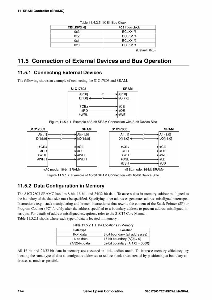
11 SRAM Controller (SRAMC)
11-4 Seiko Epson Corporation S1C17803 TECHNICAL MANUAL
Table 11.4.2.3 #CE1 Bus ClockCE1_DIV[1:0] #CE1 bus clock
0x3 BCLK•1/80x2 BCLK•1/40x1 BCLK•1/20x0 BCLK•1/1
(Default: 0x0)
11.5 Connection of External Devices and Bus Operation
11.5.1 Connecting External Devices
The following shows an example of connecting the S1C17803 and SRAM.
S1C17803
A[n:0]D[7:0]
#CEx#RD
#WRL
SRAM
A[n:0]I/O[7:0]
#CE#OE#WE
Figure 11.5.1.1 Example of 8-bit SRAM Connection with 8-bit Device Size
S1C17803
<A0 mode, 16-bit SRAM>
A[n:1]D[15:0]
#CEx#RD
#WRL#WRH
SRAM
A[n-1:0]I/O[15:0]
#CE#OE#WEL#WEH
S1C17803
<BSL mode, 16-bit SRAM>
A[n:1]D[15:0]
#CEx#RD#WR#BSL#BSH
SRAM
A[n-1:0]I/O[15:0]
#CE#OE#WE#LB#UB
Figure 11.5.1.2 Example of 16-bit SRAM Connection with 16-bit Device Size
11.5.2 Data Configuration in Memory
The S1C17803 SRAMC handles 8-bit, 16-bit, and 24/32-bit data. To access data in memory, addresses aligned to the boundary of the data size must be specified. Specifying other addresses generates address misaligned interrupts. Instructions (e.g., stack manipulating and branch instructions) that rewrite the content of the Stack Pointer (SP) or Program Counter (PC) forcibly alter the address specified to a boundary address to prevent address misaligned in-terrupts. For details of address misaligned exceptions, refer to the S1C17 Core Manual.Table 11.5.2.1 shows where each type of data is located in memory.
Table 11.5.2.1 Data Locations in MemoryData type Location
8-bit data 8-bit boundary (all addresses)16-bit data 16-bit boundary (A[0] = 0)
24/32-bit data 32-bit boundary (A[1:0] = 0b00)
All 16-bit and 24/32-bit data in memory are accessed in little endian mode. To increase memory efficiency, try locating the same type of data at contiguous addresses to reduce blank areas created by positioning at boundary ad-dresses as much as possible.
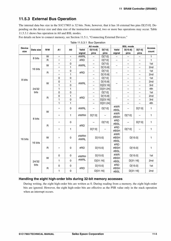
11 SRAM Controller (SRAMC)
S1C17803 TECHNICAL MANUAL Seiko Epson Corporation 11-5
11.5.3 External Bus Operation
The internal data bus size in the S1C17803 is 32 bits. Note, however, that it has 16 external bus pins D[15:0]. De-pending on the device size and data size of the instruction executed, two or more bus operations may occur. Table 11.5.3.1 shows bus operation in A0 and BSL modes. For details on how to connect memory, see Section 11.5.1, “Connecting External Devices.”
Table 11.5.3.1 Bus Operation
Device size
Data size R/W A1 A0A0 mode BSL mode
Access count
Valid signal
D[15:8] pins
D[7:0] pins
Valid signal
D[15:8] pins
D[7:0] pins
8 bits
8 bitsW * * #WRL – D[7:0] – – – 1R * * #RD – D[7:0] – – – 1
16 bitsW
* 0#WRL
– D[7:0]–
– – 1st* 1 – D[15:8] – – 2nd
R* 0
#RD– D[7:0]
–– – 1st
* 1 – D[15:8] – – 2nd
24/32 bits
W
0 0
#WRL
– D[7:0]
–
– – 1st0 1 – D[15:8] – – 2nd1 0 – D[23:16] – – 3rd1 1 – D[31:24] – – 4th
R
0 0
#RD
– D[7:0]
–
– – 1st0 1 – D[15:8] – – 2nd1 0 – D[23:16] – – 3rd1 1 – D[31:24] – – 4th
16 bits
8 bits
W* 0 #WRL – D[7:0]
#WR#BSL
– D[7:0] 1
* 1 #WRH D[7:0] –#WR#BSH
D[7:0] – 1
R* 0
#RD– D[7:0]
#RD#BSL
– D[7:0] 1
* 1 D[7:0] –#RD
#BSHD[7:0] – 1
16 bits
W * 0#WRH#WRL
D[15:0]#WR#BSH#BSL
D[15:0] 1
R * 0 #RD D[15:0]#RD
#BSH#BSL
D[15:0] 1
24/32 bits
W0 0 #WRH
#WRL
D[15:0] #WR#BSH#BSL
D[15:0] 1st
1 0 D[31:16] D[31:16] 2nd
R0 0
#RDD[15:0] #RD
#BSH#BSL
D[15:0] 1st
1 0 D[31:16] D[31:16] 2nd
Handling the eight high-order bits during 32-bit memory accesses During writing, the eight high-order bits are written as 0. During reading from a memory, the eight high-order
bits are ignored. However, the eight high-order bits are effective as the PSR value only in the stack operation when an interrupt occurs.

11 SRAM Controller (SRAMC)
11-6 Seiko Epson Corporation S1C17803 TECHNICAL MANUAL
11.6 Bus Access Timing Chart
11.6.1 SRAM Read/Write Timings with No External #WAIT
1. SRAM read/write timings with no static wait cycles [Example settings] Device size: 16 bits Access size: 16 bits Number of static wait cycles: 0 cycles CLK: BCLK (#CE0, #CE2, #CE3), BCLK•1/1–1/8 (#CE1)
CLK
A[22:0]
#CEx
#RD
D[15:0]
#WAIT
valid
valid
Figure 11.6.1.1 SRAM Read Timing with No Static Wait Cycle
CLK
A[22:0]
#CEx
#WR*
D[15:0]
#WAIT
valid
valid
Figure 11.6.1.2 SRAM Write Timing with No Static Wait Cycle

11 SRAM Controller (SRAMC)
S1C17803 TECHNICAL MANUAL Seiko Epson Corporation 11-7
2. SRAM read/write timings with static wait cycles [Example settings] Device size: 16 bits Access size: 16 bits Number of static wait cycles: 2 cycles CLK: BCLK (#CE0, #CE2, #CE3), BCLK•1/1–1/8 (#CE1)
CLK
A[22:0]
#CEx
#RD
D[15:0]
#WAIT
valid
valid
Static wait cycle
Figure 11.6.1.3 SRAM Read Timing with Static Wait Cycle
CLK
A[22:0]
#CEx
#WR*
D[15:0]
#WAIT
valid
valid
Static wait cycle
Figure 11.6.1.4 SRAM Write Timing with Static Wait Cycle

11 SRAM Controller (SRAMC)
11-8 Seiko Epson Corporation S1C17803 TECHNICAL MANUAL
11.6.2 SRAM Read/Write Timings with External #WAIT
A wait cycle can be inserted from the #WAIT pin only for SRAM-type devices.The external #WAIT signal is sampled on the rising edges of the clock at one clock before the read or write signal goes high. A wait state is entered while the #WAIT signal is sampled active (low), and subsequent operation re-sumes when the #WAIT signal is sampled inactive (high). [Example settings] Device size: 16 bits Access size: 16 bits Number of static wait cycles: 0 cycles CLK: BCLK (#CE0, #CE2, #CE3), BCLK•1/1–1/8 (#CE1)
CLK
A[22:0]
#CEx
#RD
D[15:0]
#WAIT
valid
valid
Wait cycle
Figure 11.6.2.1 SRAM Read Timing with External #WAIT
CLK
A[22:0]
#CEx
#WR*
D[15:0]
#WAIT
valid
valid
Wait cycle
Figure 11.6.2.2 SRAM Write Timing with External #WAIT
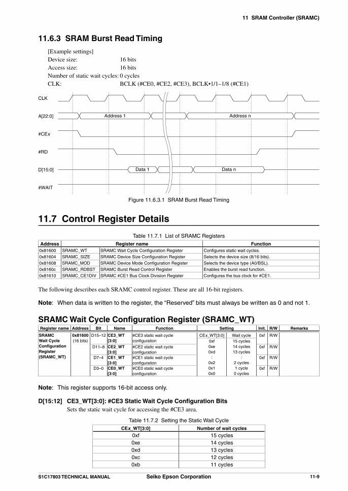
11 SRAM Controller (SRAMC)
S1C17803 TECHNICAL MANUAL Seiko Epson Corporation 11-9
11.6.3 SRAM Burst Read Timing
[Example settings] Device size: 16 bits Access size: 16 bits Number of static wait cycles: 0 cycles CLK: BCLK (#CE0, #CE2, #CE3), BCLK•1/1–1/8 (#CE1)
CLK
A[22:0]
#CEx
#RD
D[15:0]
#WAIT
Address 1 Address n
Data 1 Data n
Figure 11.6.3.1 SRAM Burst Read Timing
11.7 Control Register Details
Table 11.7.1 List of SRAMC RegistersAddress Register name Function0x81600 SRAMC_WT SRAMC Wait Cycle Configuration Register Configures static wait cycles.0x81604 SRAMC_SIZE SRAMC Device Size Configuration Register Selects the device size (8/16 bits).0x81608 SRAMC_MOD SRAMC Device Mode Configuration Register Selects the device type (A0/BSL).0x8160c SRAMC_RDBST SRAMC Burst Read Control Register Enables the burst read function.0x81610 SRAMC_CE1DIV SRAMC #CE1 Bus Clock Division Register Configures the bus clock for #CE1.
The following describes each SRAMC control register. These are all 16-bit registers.
Note: When data is written to the register, the “Reserved” bits must always be written as 0 and not 1.
SRAMC Wait Cycle Configuration Register (SRAMC_WT)Register name Address Bit Name Function Setting Init. R/W Remarks
SRAMC Wait Cycle ConfigurationRegister(SRAMC_WT)
0x81600(16 bits)
D15–12 CE3_WT[3:0]
#CE3 static wait cycle configuration
CEx_WT[3:0] Wait cycle 0xf R/W0xf0xe0xd
:0x20x10x0
15 cycles14 cycles13 cycles
:2 cycles1 cycle0 cycles
D11–8 CE2_WT[3:0]
#CE2 static wait cycle configuration
0xf R/W
D7–4 CE1_WT[3:0]
#CE1 static wait cycle configuration
0xf R/W
D3–0 CE0_WT[3:0]
#CE0 static wait cycle configuration
0xf R/W
Note: This register supports 16-bit access only.
D[15:12] CE3_WT[3:0]: #CE3 Static Wait Cycle Configuration Bits Sets the static wait cycle for accessing the #CE3 area.
Table 11.7.2 Setting the Static Wait Cycle CEx_WT[3:0] Number of wait cycles
0xf 15 cycles0xe 14 cycles0xd 13 cycles0xc 12 cycles0xb 11 cycles

11 SRAM Controller (SRAMC)
11-10 Seiko Epson Corporation S1C17803 TECHNICAL MANUAL
CEx_WT[3:0] Number of wait cycles
0xa 10 cycles0x9 9 cycles0x8 8 cycles0x7 7 cycles0x6 6 cycles0x5 5 cycles0x4 4 cycles0x3 3 cycles0x2 2 cycles0x1 1 cycle0x0 0 cycles
(Default: 0xf)
D[11:8] CE2_WT[3:0]: #CE2 Static Wait Cycle Configuration Bits Sets the static wait cycle for accessing the #CE2 area.
D[7:4] CE1_WT[3:0]: #CE1 Static Wait Cycle Configuration Bits Sets the static wait cycle for accessing the #CE1 area.
D[3:0] CE0_WT[3:0]: #CE0 Static Wait Cycle Configuration Bits Sets the static wait cycle for accessing the #CE0 area.
SRAMC Device Size Configuration Register (SRAMC_SIZE)Register name Address Bit Name Function Setting Init. R/W Remarks
SRAMC Device Size Configuration Register(SRAMC_SIZE)
0x81604(16 bits)
D15–4 – reserved – – – 0 when being read.D3 CE3_SZ #CE3 device size configuration 1 16 bits 0 8 bits 0 R/WD2 CE2_SZ #CE2 device size configuration 1 16 bits 0 8 bits 0 R/WD1 CE1_SZ #CE1 device size configuration 1 16 bits 0 8 bits 0 R/WD0 CE0_SZ #CE0 device size configuration 1 16 bits 0 8 bits 0 R/W
D[15:4] Reserved
D3 CE3_SZ: #CE3 Device Size Configuration Bit Selects the device size for the #CE3 area. 1 (R/W): 16 bits 0 (R/W): 8 bits (default)
D2 CE2_SZ: #CE2 Device Size Configuration Bit Selects the device size for the #CE2 area. 1 (R/W): 16 bits 0 (R/W): 8 bits (default)
D1 CE1_SZ: #CE1 Device Size Configuration Bit Selects the device size for the #CE1 area. 1 (R/W): 16 bits 0 (R/W): 8 bits (default)
D0 CE0_SZ: #CE0 Device Size Configuration Bit Selects the device size for the #CE0 area. 1 (R/W): 16 bits 0 (R/W): 8 bits (default)
SRAMC Device Mode Configuration Register (SRAMC_MOD)Register name Address Bit Name Function Setting Init. R/W Remarks
SRAMCDevice Mode Configuration Register(SRAMC_MOD)
0x81608(16 bits)
D15–4 – reserved – – – 0 when being read.D3 CE3_MOD #CE3 device mode configuration 1 BSL 0 A0 0 R/WD2 CE2_MOD #CE2 device mode configuration 1 BSL 0 A0 0 R/WD1 CE1_MOD #CE1 device mode configuration 1 BSL 0 A0 0 R/WD0 CE0_MOD #CE0 device mode configuration 1 BSL 0 A0 0 R/W
D[15:4] Reserved

11 SRAM Controller (SRAMC)
S1C17803 TECHNICAL MANUAL Seiko Epson Corporation 11-11
D3 CE3_MOD: #CE3 Device Mode Configuration Bit Selects a device type (A0 or BSL) for the #CE3 area. 1 (R/W): BSL 0 (R/W): A0 (default)
Table 11.7.3 Bus Control Signal Pin Functions in A0/BSL ModePin name A0 (default) BSL
#CEx #CEx #CEx#RD #RD #RDA0/#BSL A0 #BSL#WRL/#WR #WRL #WR#WRH/#BSH #WRH #BSH
D2 CE2_MOD: #CE2 Device Mode Configuration Bit Selects a device type (A0 or BSL) for the #CE2 area. 1 (R/W): BSL 0 (R/W): A0 (default)
D1 CE1_MOD: #CE1 Device Mode Configuration Bit Selects a device type (A0 or BSL) for the #CE1 area. 1 (R/W): BSL 0 (R/W): A0 (default)
D0 CE0_MOD: #CE0 Device Mode Configuration Bit Selects a device type (A0 or BSL) for the #CE0 area. 1 (R/W): BSL 0 (R/W): A0 (default)
SRAMC Burst Read Control Register (SRAMC_RDBST)Register name Address Bit Name Function Setting Init. R/W Remarks
SRAMCBurst Read Control Register(SRAMC_RDBST)
0x8160c(16 bits)
D15–4 – reserved – – – 0 when being read.D3 CE3_RDBST #CE3 burst read enable 1 Disable 0 Enable 0 R/WD2 CE2_RDBST #CE2 burst read enable 1 Disable 0 Enable 0 R/WD1 CE1_RDBST #CE1 burst read enable 1 Disable 0 Enable 0 R/WD0 CE0_RDBST #CE0 burst read enable 1 Disable 0 Enable 0 R/W
D[15:4] Reserved
D3 CE3_RDBST: #CE3 Burst Read Enable Bit Enables the burst read function for the #CE3 area. 1 (R/W): Disabled 0 (R/W): Enabled (default)
When the burst read function is enabled, the SRAMC can read the external memory successively with-out inserting setup and hold cycles (a setup cycle is inserted only in the first read cycle and a hold cycle is inserted only in the last read cycle).
D2 CE2_RDBST: #CE2 Burst Read Enable Bit Enables the burst read function for the #CE2 area. 1 (R/W): Disabled 0 (R/W): Enabled (default)
D1 CE1_RDBST: #CE1 Burst Read Enable Bit Enables the burst read function for the #CE1 area. 1 (R/W): Disabled 0 (R/W): Enabled (default)
D0 CE0_RDBST: #CE0 Burst Read Enable Bit Enables the burst read function for the #CE0 area. 1 (R/W): Disabled 0 (R/W): Enabled (default)

11 SRAM Controller (SRAMC)
11-12 Seiko Epson Corporation S1C17803 TECHNICAL MANUAL
SRAMC #CE1 Bus Clock Division Register (SRAMC_CE1DIV)Register name Address Bit Name Function Setting Init. R/W Remarks
SRAMC #CE1 Bus Clock Division Register(SRAMC_CE1DIV)
0x81610(16 bits)
D15–2 – reserved – – – 0 when being read.D1–0 CE1_DIV
[1:0]#CE1 bus clock division ratio select
CE1_DIV[1:0] Bus clock 0x0 R/W0x30x20x10x0
BCLK•1/8BCLK•1/4BCLK•1/2BCLK•1/1
D[15:2] Reserved
D[1:0] CE1_DIV[1:0]: #CE1 Bus Clock Division Ratio Select Bits Selects the bus clock used for the #CE1 area. The setup time and hold time are fixed at 1 cycle (BCLK) in the SRAMC. To connect a low-speed de-
vice that needs a more longer setup or hold time, a low-speed bus clock should be selected using CE1_DIV[1:0].
Table 11.7.4 #CE1 Bus ClockCE1_DIV[1:0] #CE1 bus clock
0x3 BCLK•1/80x2 BCLK•1/40x1 BCLK•1/20x0 BCLK•1/1
(Default: 0x0)
11.8 PrecautionsWhen the CPU accesses an external memory area (#CE0 to #CE3 areas, addresses 0x100000 to 0xfeffff) in the S1C17803 memory space, the external bus outputs the address as follows:
#CE3 area
CPU access address
CPU access address
External address bus connected to a 1MB deviceExternal address bus connected to a 2MB deviceExternal address bus connected to a 4MB deviceExternal address bus connected to an 8MB device
Not output to the external bus
0xfe ffff [1111 1110 1111 1111 1111 1111]
0xf0 0000 [1111 0000 0000 0000 0000 0000]0xef ffff [1110 1111 1111 1111 1111 1111]
0x70 0000 [0111 0000 0000 0000 0000 0000]0x6f ffff [0110 1111 1111 1111 1111 1111]
0x30 0000 [0011 0000 0000 0000 0000 0000]0x2f ffff [0010 1111 1111 1111 1111 1111]
0x10 0000 [0001 0000 0000 0000 0000 0000]
0xef ffff [1110 1111 1111 1111 1111 1111]: :::: :::: :::: :::: :::: ::::
0x80 0000 [1000 0000 0000 0000 0000 0000]0x7f ffff [0111 1111 1111 1111 1111 1111]
: :::: :::: :::: :::: :::: :::: 0x70 0000 [0111 0000 0000 0000 0000 0000]
Address of the external memory0x7f ffff [111 1111 1111 1111 1111 1111]
: :::: :::: :::: :::: :::: :::: 0x70 0000 [111 0000 0000 0000 0000 0000]0x6f ffff [110 1111 1111 1111 1111 1111]
: :::: :::: :::: :::: :::: :::: 0x00 0000 [000 0000 0000 0000 0000 0000]
#CE2 area
#CE1 area
#CE0 area
Example: when an 8MB memory is connected to the #CE2 area
#CE2 area
A0A19
A0A23
A0A20A0A21A0A22
Table 11.8.1 CPU Access Address and External Bus Output Address
For example, the address to be accessed will be directly output on the external bus when the CPU accesses an ad-dress within the range from 0x700000 to 0x7fffff in the #CE2 area. When the CPU accesses an address within the range from 0x800000 to 0xefffff (the high-order 7MB of the #CE2 area), the external bus outputs an address within the range from 0x000000 to 0x6fffff (the low-order 7MB of the external memory device will be accessed), as the external address bus does not have A23. In other words, the relative address from beginning of the #CE2 area may not correspond to the address of the external memory device.

11 SRAM Controller (SRAMC)
S1C17803 TECHNICAL MANUAL Seiko Epson Corporation 11-13
There is no problem when an SRAM is connected to the external bus. Take this into consideration if a ROM in which data has been written externally is connected. Furthermore, when a Flash memory is connected to the ex-ternal bus, pay attention to the correspondence between the sector to be accessed and the address accessed by the CPU, as the sector size is not the same in all sectors.

12 Interrupt Controller (ITC)
S1C17803 TECHNICAL MANUAL Seiko Epson Corporation 12-1
12 Interrupt Controller (ITC)
12.1 ITC Module OverviewThe S1C17803 provides the interrupt systems listed below.
1. DMA interrupt (1 type)2. Port interrupt 0 (7 types) 3. Port interrupt 1 (6 types) 4. 16-bit PWM timer interrupt (6 types) 5. USI Ch.0 interrupt (3 types) 6. USI Ch.1 interrupt (3 types) 7. A/D converter interrupt (2 types) 8. 16-bit audio PWM timer interrupt (3 types)9. I2S interrupt (3 types)10. LCDC interrupt (1 type)11. CLG_T16FU0 interrupt (1 type)12. CLG_T8I interrupt (1 type)13. UART interrupt (3 types)14. I2C master interrupt (2 types)15. I2C slave interrupt (3 types)16. 8-bit programmable timer interrupt (3 types)17. RTC interrupt (1 type)18. Remote controller interrupt (3 types)
The ITC enables the interrupt level (priority) for determining the processing sequence when multiple interrupts oc-cur simultaneously to be set for each interrupt system separately.Each interrupt system includes the number of interrupt causes indicated in parentheses above. Settings to enable or disable interrupt for different causes are set by the respective peripheral module registers.For specific information on interrupt causes and their control, refer to the peripheral module explanations.Figure 12.1.1 shows the structure of the interrupt system.
S1C17 Core Interrupt controller
Watchdog timer
Interrupt request
Interruptlevel
Vectornumber
Debug signalReset signal
Interrupt request
NMI
Interrupt level
Interruptcontrol
Vector number
Interrupt level
Vector number
Interrupt request
• •
• •
•
• •
•
Peripheral module
Interrupt enable
Cause of interrupt 1
Interrupt enable
Cause of interrupt n
• •
• •
Interrupt flag
Interrupt flag
Peripheral module
Interrupt enable
Cause of interrupt 1
Interrupt enable
Cause of interrupt n
• •
• •
Interrupt flag
Interrupt flag
Figure 12.1.1 Interrupt System

12 Interrupt Controller (ITC)
12-2 Seiko Epson Corporation S1C17803 TECHNICAL MANUAL
12.2 Vector TableThe vector table contains the vectors to the interrupt handler routines (handler routine start address) that will be read by the S1C17 Core to execute the handler when an interrupt occurs. Table 12.2.1 shows the vector table of the S1C17803.
Table 12.2.1 Vector TableVector No.
Software interrupt No.Vector
addressHardware interrupt name Cause of hardware interrupt Priority
0 (0x00) TTBR + 0x00 Reset • Low input to the #RESET pin• Watchdog timer overflow *2
1
1 (0x01) TTBR + 0x04 Address misaligned interrupt Memory access instruction 2– (0xfffc00) Debugging interrupt brk instruction, etc. 3
2 (0x02) TTBR + 0x08 NMI • Low input to the #NMI pin• Watchdog timer overflow *2
4
3 (0x03) TTBR + 0x0c reserved – –4 (0x04) TTBR + 0x10 DMAC interrupt End of DMA transfer High *1
5 (0x05) TTBR + 0x14 Port interrupt 0 P2/P8 input (rising/falling edge or high/low level) ↑6 (0x06) TTBR + 0x18 Port interrupt 1 PA/P4 input (rising/falling edge or high/low level)
16-bit PWM timer interrupt • Compare A/B• Capture A/B• Capture A/B overwrite
7 (0x07) TTBR + 0x1c USI Ch.0 interrupt • Transmit buffer empty• Receive buffer full• Receive error
8 (0x08) TTBR + 0x20 USI Ch.1 interrupt • Transmit buffer empty• Receive buffer full• Receive error
9 (0x09) TTBR + 0x24 A/D converter interrupt • Conversion completion• Conversion result overwrite
10 (0x0a) TTBR + 0x28 16-bit audio PWM timer interrupt • Compare A/B• Buffer empty
I2S interrupt I2S FIFO whole/half/one empty11 (0x0b) TTBR + 0x2c LCDC interrupt Frame signal12 (0x0c) TTBR + 0x30 CLG_T16FU0 interrupt Timer underflow13 (0x0d) TTBR + 0x34
reserved –14 (0x0e) TTBR + 0x3815 (0x0f) TTBR + 0x3c CLG_T8I interrupt Timer underflow16 (0x10) TTBR + 0x40 UART interrupt • Transmit buffer empty
• Receive buffer full• Receive error
17 (0x11) TTBR + 0x44reserved –
18 (0x12) TTBR + 0x4819 (0x13) TTBR + 0x4c I2C Master interrupt • Transmit buffer empty
• Receive buffer full20 (0x14) TTBR + 0x50 I2C Slave interrupt • Transmit buffer empty
• Receive buffer full• Bus status
21 (0x15) TTBR + 0x54 8-bit programmable timer Ch.0–Ch.2 interrupt
Timer Ch.0/Ch.1/Ch.2 underflow
16-bit PWM timer interrupt • Compare A/B• Capture A/B• Capture A/B overwrite
22 (0x16) TTBR + 0x58 RTC interrupt 1/64 second, 1 second, 1 minute, or 1 hourcount up
23 (0x17) TTBR + 0x5c Remote controller interrupt • Data length counter underflow• Input rising edge detected• Input falling edge detected
24 (0x18) TTBR + 0x60reserved –: : ↓
31 (0x1f) TTBR + 0x7c Low *1
*1 When the same interrupt level is set*2 Either reset or NMI can be selected as the watchdog timer interrupt with software.
Vector numbers 4 to 23 are assigned to the maskable interrupts supported by the S1C17803.

12 Interrupt Controller (ITC)
S1C17803 TECHNICAL MANUAL Seiko Epson Corporation 12-3
Interrupts that share an interrupt vector Interrupt vector numbers 6, 10, and 21 are shared with two different interrupt modules. Interrupt vector 6: Port interrupt 1 and 16-bit PWM timer Interrupt vector 10: 16-bit audio PWM timer and I2S Interrupt vector 21: 8-bit programmable timer and 16-bit PWM timer
The interrupt signals from the two modules are input to the ITC through an OR gate. The 16-bit audio PWM timer and I2S interrupts that share interrupt vector 10 can be used simultaneously. The
interrupt vector 10 handler routine should check which interrupt has occurred by reading the interrupt flags in the 16-bit audio PWM timer and I2S modules.
The three interrupts, port interrupt 1, 16-bit PWM timer and 8-bit programmable timer interrupts, that are as-signed to interrupt vectors 6 and 21 cannot be used simultaneously. Any two of them can be used simultane-ously.
To use port interrupt 1 and 16-bit PWM timer interrupts, disable 8-bit programmable timer interrupts and set the interrupt level of vector 21 higher than that of vector 6. When a 16-bit PWM timer interrupt occurs, the in-terrupt vector 21 handler routine is executed.
To use 8-bit programmable timer and 16-bit PWM timer interrupts, disable port interrupt 1 and set the interrupt level of vector 6 higher than that of vector 21. When a 16-bit PWM timer interrupt occurs, the interrupt vector 6 handler routine is executed.
To use port interrupt 1 and 8-bit programmable timer interrupts, disable 16-bit PWM timer interrupts.
Vector table base address The S1C17803 allows the base (starting) address of the vector table to be set using the MISC_TTBRL and
MISC_TTBRH registers. “TTBR” described in Table 12.2.1 means the value set to these registers. After an ini-tial reset, the MISC_TTBRL and MISC_TTBRH registers are set to 0x8000. Therefore, even when the vector table location is changed, it is necessary that at least the reset vector be written to the above address. Bits 7 to 0 in the MISC_TTBRL register are fixed at 0, so the vector table always begins with a 256-byte boundary ad-dress.
Vector Table Address Low/High Registers (MISC_TTBRL, MISC_TTBRH)Register name Address Bit Name Function Setting Init. R/W Remarks
Vector Table Address Low Register(MISC_TTBRL)
0x5328(16 bits)
D15–8 TTBR[15:8] Vector table base address A[15:8] 0x0–0xff 0x80 R/W Write-protectedD7–0 TTBR[7:0] Vector table base address A[7:0]
(fixed at 0)0x0 0x0 R
Vector Table Address High Register (MISC_TTBRH)
0x532a(16 bits)
D15–8 – reserved – – – 0 when being read.D7–0 TTBR[23:16] Vector table base address
A[23:16]0x0–0xff 0x0 R/W Write-protected
Note: The MISC_TTBRL and MISC_TTBRH registers are write-protected. Before these registers can be rewritten, write protection must be removed by writing data 0x96 to the MISC_PROT register. Note that since unnecessary rewrites to the MISC_TTBRL and MISC_TTBRH registers could lead to erratic system operation, the MISC_PROT register should be set to other than 0x96 unless the Vector Table Base Registers must be rewritten.
12.3 Control of Maskable Interrupts
12.3.1 Interrupt Control Bits in Peripheral ModulesThe peripheral module that generates an interrupts includes an interrupt enable bit and an interrupt flag for each interrupt cause. The interrupt flag is set to 1 when the cause of interrupt occurs. By setting the interrupt enable bit to 1 (interrupt enabled), the flag state will be sent to the ITC as an interrupt request signal, generating an interrupt request to the S1C17 Core. The corresponding interrupt enable bits should be set to 0 for those causes for which interrupts are not desired. In this case, although the interrupt flag is set to 1 if the interrupt cause occurs, the interrupt request signal sent to the ITC will not be asserted.
12 Interrupt Controller (ITC)
12-4 Seiko Epson Corporation S1C17803 TECHNICAL MANUAL
The interrupt flag set to 1 must be reset in the interrupt handler routine after the interrupt has occurred. The ITC will generate the same interrupt again once the interrupt handler routine has been ended by the reti instruction with the interrupt flag still set to 1, since it detects interrupt requests using the signal level.For specific information on causes of interrupts, interrupt flags, and interrupt enable bits, refer to the respective pe-ripheral module descriptions.
12.3.2 ITC Interrupt Request Processing
On receiving an interrupt signal from a peripheral module, the ITC sends the interrupt request, interrupt level, and vector number signals to the S1C17 Core.Vector numbers are determined by the ITC internal hardware for each interrupt cause, as shown in Table 12.2.1.The interrupt level is a value used by the S1C17 Core to compare with the IL bits (PSR). This interrupt level is usedin the S1C17 Core to disable subsequently occurring interrupts with the same or lower level. (See Section 12.3.3.)The default ITC settings are level 0 for all maskable interrupts. Interrupt requests are not accepted by the S1C17 Core if the level is 0.The ITC includes control bits for selecting the interrupt level, and the level can be set to between 0 (low) and 7 (high)interrupt levels for each interrupt vector.If interrupt requests are input to the ITC simultaneously from two or more peripheral modules, the ITC outputs the interrupt request with the highest priority to the S1C17 Core in accordance with the following conditions.1. The interrupt with the highest interrupt level takes precedence.2. If multiple interrupt requests are input with the same interrupt level, the interrupt with the lowest vector number
takes precedence.
The other interrupts occurring at the same time are held until all interrupts with higher priority levels have been ac-cepted by the S1C17 Core.If an interrupt cause with higher priority occurs while the ITC is outputting an interrupt request signal to the S1C17Core (before being accepted by the S1C17 core), the ITC alters the vector number and interrupt level signals to the setting information on the more recent interrupt. The previously occurring interrupt is held. The held interrupt is canceled and no interrupt is generated if the interrupt flag in the peripheral module is reset with software.
Table 12.3.2.1 Interrupt Level Setting BitsHardware interrupt Interrupt level setting bits Register address
DMA interrupt ILV0[2:0] (D[2:0]/ITC_LV0 register) 0x42e6Port interrupt 0 ILV1[2:0] (D[10:8]/ITC_LV0 register) 0x42e6Port interrupt 1 / 16-bit PWM timer interrupt ILV2[2:0] (D[2:0]/ITC_LV1 register) 0x42e8USI Ch.0 interrupt ILV3[2:0] (D[10:8]/ITC_LV1 register) 0x42e8USI Ch.1 interrupt ILV4[2:0] (D[2:0]/ITC_LV2 register) 0x42eaA/D converter interrupt ILV5[2:0] (D[10:8]/ITC_LV2 register) 0x42ea16-bit audio PWM timer interrupt / I2S interrupt ILV6[2:0] (D[2:0]/ITC_LV3 register) 0x42ecLCDC interrupt ILV7[2:0] (D[10:8]/ITC_LV3 register) 0x42ecCLG_T16FU0 interrupt ILV8[2:0] (D[2:0]/ITC_LV4 register) 0x42eeCLG_T8I interrupt ILV11[2:0] (D[10:8]/ITC_LV5 register) 0x42f0UART interrupt ILV12[2:0] (D[2:0]/ITC_LV6 register) 0x42f2I2C master interrupt ILV15[2:0] (D[10:8]/ITC_LV7 register) 0x42f4I2C slave interrupt ILV16[2:0] (D[2:0]/ITC_LV8 register) 0x42f68-bit programmable timer Ch.0–Ch.2 / 16-bit PWM timer interrupt
ILV17[2:0] (D[10:8]/ITC_LV8 register) 0x42f6
RTC interrupt ILV18[2:0] (D[2:0]/ITC_LV9 register) 0x42f8Remote controller interrupt ILV19[2:0] (D[10:8]/ITC_LV9 register) 0x42f8
12.3.3 Interrupt Processing by the S1C17 Core
A Maskable interrupt to the S1C17 Core occurs when all of the following conditions are met:
• The interrupt is enabled by the interrupt control bit inside the peripheral module.
• The IE (Interrupt Enable) bit of the PSR (Processor Status Register) in the S1C17 Core has been set to 1.
• The cause of interrupt that has occurred has a higher interrupt level than the value set in the IL field of the PSR.
• No other cause of interrupt having higher priority, such as NMI, has occurred.

12 Interrupt Controller (ITC)
S1C17803 TECHNICAL MANUAL Seiko Epson Corporation 12-5
If an interrupt cause that has been enabled in the peripheral module occurs, the corresponding interrupt flag is set to 1, and this state is maintained until it is reset by the program. This means that the interrupt cause is not cleared even if the conditions listed above are not met when the interrupt cause occurs. An interrupt occurs if the above conditions are met.If multiple maskable interrupt causes occur simultaneously, the interrupt cause with the highest interrupt level and lowest vector number becomes the subject of the interrupt request to the S1C17 Core. Interrupts with lower levels are held until the above conditions are subsequently met.
The S1C17 Core samples interrupt requests for each cycle. On accepting an interrupt request, the S1C17 Core switches to interrupt processing immediately after execution of the current instruction has been completed.Interrupt processing involves the following steps:(1) The PSR and current program counter (PC) values are saved to the stack.(2) The PSR IE bit is reset to 0 (disabling subsequent maskable interrupts).(3) The PSR IL bits are set to the received interrupt level. (The NMI does not affect the IL bits.)(4) The vector for the interrupt occurred is loaded to the PC to execute the interrupt handler routine.
When an interrupt is received, (2) prevents subsequent maskable interrupts. Setting the IE bit to 1 in the interrupt handler routine allows handling of multiple interrupts. In this case, since IL is changed by (3), only an interrupt with a higher level than that of the currently processed interrupt will be accepted. Ending interrupt handler routines using the reti instruction returns the PSR to the state before the interrupt has occurred. The program resumes pro-cessing following the instruction being executed at the time the interrupt occurred.
12.4 NMIIn the S1C17803, a low level input to the #NMI pin or the watchdog timer can generate a non-maskable interrupt (NMI). The vector number for NMI is 2, with the vector address set to the vector table's starting address + 8 bytes. This interrupt takes precedence over other interrupts and is unconditionally accepted by the S1C17 Core. For detailed information on generating NMI by the watchdog timer, see the “Watchdog Timer (WDT)” chapter.
12.5 Software InterruptsThe S1C17 Core provides the “int imm5” and “intl imm5,imm3” instructions allowing the software to gener-ate any interrupts. The operand imm5 specifies a vector number (0–31) in the vector table. In addition to this, the intl instruction has the operand imm3 to specify the interrupt level (0–7) to be set to the IL field in the PSR.The processor performs the same interrupt processing as that of the hardware interrupt.
12.6 HALT and SLEEP Mode CancellationHALT mode is cleared by the following signals, which start the CPU.• Interrupt request signal sent to the CPU from the ITC• NMI signal output by the watchdog timer or input to the #NMI pin• Debug interrupt signal• Reset signal output by the watchdog timer or input to the #RESET pin
SLEEP mode is cleared by the following signals, which start the CPU.• Port interrupt 0, port interrupt 1 or RTC interrupt request signal sent from the GPIO or RTC• NMI signal input to the #NMI pin• Reset signal input to the #RESET pin
Notes: • If the CPU is able to receive interrupts when HALT or SLEEP mode has been cleared by an interrupt request for the CPU from the ITC, processing branches to the interrupt handler rou-tine immediately after cancellation. In all other cases, the program is executed following the halt or slp instruction.
• HALT or SLEEP mode clearing due to interrupt requests cannot be masked (prohibited) using ITC interrupt level settings. When using a cause of interrupt to clear HALT or SLEEP mode, the interrupt enable bit corresponding to the cause of interrupt must be set to 1 (interrupt enabled).
For more information, see “Power Saving by Clock Control” in Appendix.

12 Interrupt Controller (ITC)
12-6 Seiko Epson Corporation S1C17803 TECHNICAL MANUAL
12.7 Control Register Details
Table 12.7.1 List of ITC RegistersAddress Register name Function0x42e6 ITC_LV0 Interrupt Level Setup Register 0 Sets the DMA and port 0 interrupt levels.0x42e8 ITC_LV1 Interrupt Level Setup Register 1 Sets the port 1/T16A and USI Ch.0 interrupt levels.0x42ea ITC_LV2 Interrupt Level Setup Register 2 Sets the USI Ch.1 and ADC interrupt levels.0x42ec ITC_LV3 Interrupt Level Setup Register 3 Sets the T16P/I2S and LCDC interrupt levels.0x42ee ITC_LV4 Interrupt Level Setup Register 4 Sets the CLG_T16FU0 interrupt level.0x42f0 ITC_LV5 Interrupt Level Setup Register 5 Sets the CLG_T8I interrupt level.0x42f2 ITC_LV6 Interrupt Level Setup Register 6 Sets the UART interrupt level.0x42f4 ITC_LV7 Interrupt Level Setup Register 7 Sets the I2CM interrupt level.0x42f6 ITC_LV8 Interrupt Level Setup Register 8 Sets the I2CS and T8F Ch.0–2/T16A interrupt levels.0x42f8 ITC_LV9 Interrupt Level Setup Register 9 Sets the RTC and REMC interrupt levels.
The ITC registers are described in detail below. These are 16-bit registers.
Note: When data is written to the registers, the “Reserved” bits must always be written as 0 and not 1.
Interrupt Level Setup Register 0 (ITC_LV0)Register name Address Bit Name Function Setting Init. R/W Remarks
Interrupt Level Setup Register 0(ITC_LV0)
0x42e6(16 bits)
D15–11 – reserved – – – 0 when being read.D10–8 ILV1[2:0] Port 0 interrupt level 0 to 7 0x0 R/WD7–3 – reserved – – – 0 when being read.D2–0 ILV0[2:0] DMA interrupt level 0 to 7 0x0 R/W
D[15:11] Reserved
D[10:8] ILV1[2:0]: Port 0 Interrupt Level Bits Sets the port 0 interrupt level (0 to 7). (Default: 0x0) The S1C17 Core does not accept interrupts with a level set lower than the PSR IL value. The ITC uses the interrupt level when multiple interrupt requests occur simultaneously. If multiple interrupt requests enabled by the interrupt enable bit occur simultaneously, the ITC sends the
interrupt request with the highest level set by the ITC_LVx registers (0x42e6 to 0x42f8) to the S1C17 Core.
If multiple interrupt requests with the same interrupt level occur simultaneously, the interrupt with the lowest vector number is processed first. The other interrupts are held until all interrupts of higher prior-ity have been accepted by the S1C17 Core.
If an interrupt requests of higher priority occurs while the ITC outputs an interrupt request signal to the S1C17 Core (before acceptance by the S1C17 Core), the ITC alters the vector number and interrupt level signals to the setting details of the most recent interrupt. The immediately preceding interrupt is held.
D[7:3] Reserved
D[2:0] ILV0[2:0]: DMA Interrupt Level Bits Sets the DMA interrupt level (0 to 7). (Default: 0x0) See the description of ILV1[2:0].
Interrupt Level Setup Register 1 (ITC_LV1)Register name Address Bit Name Function Setting Init. R/W Remarks
Interrupt Level Setup Register 1(ITC_LV1)
0x42e8(16 bits)
D15–11 – reserved – – – 0 when being read.D10–8 ILV3[2:0] USI Ch.0 interrupt level 0 to 7 0x0 R/WD7–3 – reserved – – – 0 when being read.D2–0 ILV2[2:0] Port 1/T16A interrupt level 0 to 7 0x0 R/W
D[15:11] Reserved
D[10:8] ILV3[2:0]: USI Ch.0 Interrupt Level Bits Sets the USI Ch.0 interrupt level (0 to 7). (Default: 0x0) See the description of ILV1[2:0]/ITC_LV0 register.
12 Interrupt Controller (ITC)
S1C17803 TECHNICAL MANUAL Seiko Epson Corporation 12-7
D[7:3] Reserved
D[2:0] ILV2[2:0]: Port1/T16A Interrupt Level Bits Sets the port 1 and 16-bit PWM timer interrupt levels (0 to 7). (Default: 0x0) See the description of ILV1[2:0]/ITC_LV0 register.
Interrupt Level Setup Register 2 (ITC_LV2)Register name Address Bit Name Function Setting Init. R/W Remarks
Interrupt Level Setup Register 2(ITC_LV2)
0x42ea(16 bits)
D15–11 – reserved – – – 0 when being read.D10–8 ILV5[2:0] ADC interrupt level 0 to 7 0x0 R/WD7–3 – reserved – – – 0 when being read.D2–0 ILV4[2:0] USI Ch.1 interrupt level 0 to 7 0x0 R/W
D[15:11] Reserved
D[10:8] ILV5[2:0]: ADC Interrupt Level Bits Sets the A/D converter interrupt level (0 to 7). (Default: 0x0) See the description of ILV1[2:0]/ITC_LV0 register.
D[7:3] Reserved
D[2:0] ILV4[2:0]: USI Ch.1 Interrupt Level Bits Sets the USI Ch.1 interrupt level (0 to 7). (Default: 0x0) See the description of ILV1[2:0]/ITC_LV0 register.
Interrupt Level Setup Register 3 (ITC_LV3)Register name Address Bit Name Function Setting Init. R/W Remarks
Interrupt Level Setup Register 3(ITC_LV3)
0x42ec(16 bits)
D15–11 – reserved – – – 0 when being read.D10–8 ILV7[2:0] LCDC interrupt level 0 to 7 0x0 R/WD7–3 – reserved – – – 0 when being read.D2–0 ILV6[2:0] T16P/I2S interrupt level 0 to 7 0x0 R/W
D[15:11] Reserved
D[10:8] ILV7[2:0]: LCDC Interrupt Level Bits Sets the LCDC interrupt level (0 to 7). (Default: 0x0) See the description of ILV1[2:0]/ITC_LV0 register.
D[7:3] Reserved
D[2:0] ILV6[2:0]: T16P/I2S Interrupt Level Bits Sets the 16-bit audio PWM timer and I2S interrupt levels (0 to 7). (Default: 0x0) See the description of ILV1[2:0]/ITC_LV0 register.
Interrupt Level Setup Register 4 (ITC_LV4)Register name Address Bit Name Function Setting Init. R/W Remarks
Interrupt Level Setup Register 4(ITC_LV4)
0x42ee(16 bits)
D15–3 – reserved – – – 0 when being read.
D2–0 ILV8[2:0] CLG_T16FU0 interrupt level 0 to 7 0x0 R/W
D[15:3] Reserved
D[2:0] ILV8[2:0]: CLG_T16FU0 Interrupt Level Bits Sets the CLG_T16FU0 interrupt level (0 to 7). (Default: 0x0) See the description of ILV1[2:0]/ITC_LV0 register.
Interrupt Level Setup Register 5 (ITC_LV5)Register name Address Bit Name Function Setting Init. R/W Remarks
Interrupt Level Setup Register 5(ITC_LV5)
0x42f0(16 bits)
D15–11 – reserved – – – 0 when being read.D10–8 ILV11[2:0] CLG_T8I interrupt level 0 to 7 0x0 R/WD7–0 – reserved – – – 0 when being read.

12 Interrupt Controller (ITC)
12-8 Seiko Epson Corporation S1C17803 TECHNICAL MANUAL
D[15:11] Reserved
D[10:8] ILV11[2:0]: CLG_T8I Interrupt Level Bits Sets the CLG_T8I interrupt level (0 to 7). (Default: 0x0) See the description of ILV1[2:0]/ITC_LV0 register.
D[7:0] Reserved
Interrupt Level Setup Register 6 (ITC_LV6)Register name Address Bit Name Function Setting Init. R/W Remarks
Interrupt Level Setup Register 6(ITC_LV6)
0x42f2(16 bits)
D15–3 – reserved – – – 0 when being read.
D2–0 ILV12[2:0] UART interrupt level 0 to 7 0x0 R/W
D[15:3] Reserved
D[2:0] ILV12[2:0]: UART Interrupt Level Bits Sets the UART interrupt level (0 to 7). (Default: 0x0) See the description of ILV1[2:0]/ITC_LV0 register.
Interrupt Level Setup Register 7 (ITC_LV7)Register name Address Bit Name Function Setting Init. R/W Remarks
Interrupt Level Setup Register 7(ITC_LV7)
0x42f4(16 bits)
D15–11 – reserved – – – 0 when being read.D10–8 ILV15[2:0] I2CM interrupt level 0 to 7 0x0 R/WD7–0 – reserved – – – 0 when being read.
D[15:11] Reserved
D[10:8] ILV15[2:0]: IC2CM Interrupt Level Bits Sets the I2C master interrupt level (0 to 7). (Default: 0x0) See the description of ILV1[2:0]/ITC_LV0 register.
D[7:0] Reserved
Interrupt Level Setup Register 8 (ITC_LV8)Register name Address Bit Name Function Setting Init. R/W Remarks
Interrupt Level Setup Register 8(ITC_LV8)
0x42f6(16 bits)
D15–11 – reserved – – – 0 when being read.D10–8 ILV17[2:0] T8F/T16A interrupt level 0 to 7 0x0 R/WD7–3 – reserved – – – 0 when being read.D2–0 ILV16[2:0] I2CS interrupt level 0 to 7 0x0 R/W
D[15:11] Reserved
D[10:8] ILV17[2:0]: T8F/T16A Interrupt Level Bits Sets the 8-bit programmable timer and 16-bit PWM timer interrupt levels (0 to 7). (Default: 0x0) See the description of ILV1[2:0]/ITC_LV0 register.
D[7:3] Reserved
D[2:0] ILV16[2:0]: I2CS Interrupt Level Bits Sets the I2C slave interrupt level (0 to 7). (Default: 0x0) See the description of ILV1[2:0]/ITC_LV0 register.
Interrupt Level Setup Register 9 (ITC_LV9)Register name Address Bit Name Function Setting Init. R/W Remarks
Interrupt Level Setup Register 9(ITC_LV9)
0x42f8(16 bits)
D15–11 – reserved – – – 0 when being read.D10–8 ILV19[2:0] REMC interrupt level 0 to 7 0x0 R/WD7–3 – reserved – – – 0 when being read.D2–0 ILV18[2:0] RTC interrupt level 0 to 7 0x0 R/W
D[15:11] Reserved

12 Interrupt Controller (ITC)
S1C17803 TECHNICAL MANUAL Seiko Epson Corporation 12-9
D[10:8] ILV19[2:0]: REMC Interrupt Level Bits Sets the remote controller interrupt level (0 to 7). (Default: 0x0) See the description of ILV1[2:0]/ITC_LV0 register.
D[7:3] Reserved
D[2:0] ILV18[2:0]: RTC Interrupt Level Bits Sets the RTC interrupt level (0 to 7). (Default: 0x0) See the description of ILV1[2:0]/ITC_LV0 register.
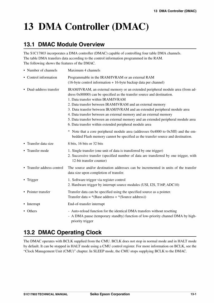
13 DMA Controller (DMAC)
S1C17803 TECHNICAL MANUAL Seiko Epson Corporation 13-1
13 DMA Controller (DMAC)
13.1 DMAC Module OverviewThe S1C17803 incorporates a DMA controller (DMAC) capable of controlling four table DMA channels.The table DMA transfers data according to the control information programmed in the RAM.The following shows the features of the DMAC.
• Number of channels Maximum 4 channels
• Control information Programmable in the IRAM/IVRAM or an external RAM (16-byte control information + 16-byte backup data per channel)
• Dual-address transfer IRAM/IVRAM, an external memory or an extended peripheral module area (from ad-dress 0x80000) can be specified as the transfer source and destination.
1. Data transfer within IRAM/IVRAM 2. Data transfer between IRAM/IVRAM and an external memory 3. Data transfer between IRAM/IVRAM and an extended peripheral module area 4. Data transfer between an external memory and an external memory 5. Data transfer between an external memory and an extended peripheral module area 6. Data transfer within extended peripheral module area
* Note that a core peripheral module area (addresses 0x4000 to 0x5fff) and the em-bedded Flash memory cannot be specified as the transfer source and destination.
• Transfer data size 8 bits, 16 bits or 32 bits
• Transfer mode 1. Single transfer (one unit of data is transferred by one trigger) 2. Successive transfer (specified number of data are transferred by one trigger, with
12-bit transfer counter)
• Transfer address control The source and/or destination addresses can be incremented in units of the transfer data size upon completion of transfer.
• Trigger 1. Software trigger via register control 2. Hardware trigger by interrupt source modules (USI, I2S, T16P, ADC10)
• Pointer transfer Transfer data can be specified using the specified source as a pointer. Transfer data = *(Base address + *(Source address))
• Interrupt End-of-transfer interrupt
• Others - Auto-reload function for the identical DMA transfers without resetting - A DMA pause (temporary standby) function of low-priority channel DMA by high-
priority trigger
13.2 DMAC Operating ClockThe DMAC operates with BCLK supplied from the CMU. BCLK does not stop in normal mode and in HALT mode by default. It can be stopped in HALT mode using a CMU control register. For more information on BCLK, see the “Clock Management Unit (CMU)” chapter. In SLEEP mode, the CMU stops supplying BCLK to the DMAC.

13 DMA Controller (DMAC)
13-2 Seiko Epson Corporation S1C17803 TECHNICAL MANUAL
13.3 Programming Control InformationThe DMAC operates according to the transfer conditions specified with control information. The control informa-tion must be programmed in IRAM/IVRAM or an external RAM. The control information size is 16 bytes per channel. When using the auto-reload function, each channel needs additional 16 bytes for storing reload data (control information resetting data). The auto-reload function resets control information, which is updated during data trans-fer, with the reload data after a DMA transfer has finished. Therefore, a consecutive 128-byte space is required for the control table to use four DMA channels.
The following explains how to set the base address of the control table and the contents of control information.
13.3.1 Setting the Base Address
The RAM area beginning with the specified base address is allocated to the control table. The base address is the start address of the control information for Ch.0 and can be specified using TBL_BASE[23:0]/DMA_TBL_BASE(H & L) registers. TBL_BASE[9:0] is fixed at 0 regardless of the contents written, therefore the base address is always set to 1,024-byte boundary address. The initial value of TBL_BASE[23:0] is 0xc0000 the start address of IRAM/IVRAM.
Base + 0x70Base + 0x60Base + 0x50Base + 0x40Base + 0x30Base + 0x20Base + 0x10
Base Ch.0 control tableCh.0 auto-reload data areaCh.1 control tableCh.1 auto-reload data areaCh.2 control tableCh.2 auto-reload data areaCh.3 control tableCh.3 auto-reload data area
Figure 13.3.1.1 Control Table Map
Note: The control table must be placed on IRAM/IVRAM or an external RAM. A Flash memory and BBRAM cannot be used to store control information.
13.3.2 Control Information
The address to store control information is determined by the base address and a channel number.
Start address of channel = base address + (channel number × 32 [bytes])
Note: The control information must be written only when the channel to be configured does not start a DMA transfer. If a DMA transfer starts when the control information is being written, proper transfer cannot be performed. Reading the control information can always be performed.
The contents of control information in each channel are shown in the table below.
Table 13.3.2.1 Control InformationWord Address Bit Name Function Setting
1st word(16 bits)
Ch.0: Base + 0x0Ch.1: Base + 0x20Ch.2: Base + 0x40Ch.3: Base + 0x60
D15–12 TC[3:0] Transfer counter(low-order 4 bits)
TC[11:0] Count0xfff
:0x10x0
4,095:1
4,096D11 ST Source type 1 Pointer 0 Data
D10–8 UNIT[2:0] Transfer data unit UNIT[2:0] Data unit0x7–0x3
0x20x10x0
reserved32 bits16 bits8 bits
D7–6 SRINC[1:0] Source address control SRINC[1:0] Address0x3–0x2
0x10x0
reservedIncrement
Fixed

13 DMA Controller (DMAC)
S1C17803 TECHNICAL MANUAL Seiko Epson Corporation 13-3
Word Address Bit Name Function Setting
1st word(16 bits)
Ch.0: Base + 0x0Ch.1: Base + 0x20Ch.2: Base + 0x40Ch.3: Base + 0x60
D5–4 DSINC[1:0] Destination address control DSINC[1:0] Address0x3–0x2
0x10x0
reservedIncrement
FixedD3 CHEN Channel enable 1 Enable 0 DisableD2 TM Transfer mode 1 Successive 0 SingleD1 RELOAD Auto-reload enable 1 Enable 0 DisableD0 PTW Pointer bit width 1 8 bits 0 16 bits
2nd word(16 bits)
Ch.0: Base + 0x2Ch.1: Base + 0x22Ch.2: Base + 0x42Ch.3: Base + 0x62
D15–8 – reserved –D7–0 TC[11:4] Transfer counter
(high-order 8 bits)TC[11:0] Count
0xfff:
0x10x0
4,095:1
4,0963rd word(16 bits)
Ch.0: Base + 0x4Ch.1: Base + 0x24Ch.2: Base + 0x44Ch.3: Base + 0x64
D15–0 SRADR[15:0] Source address/source data pointer(low-order 16 bits)
0x0 to 0xffff(SRADR[23:0] = 0x0 to 0xffffff)
4th word(16 bits)
Ch.0: Base + 0x6Ch.1: Base + 0x26Ch.2: Base + 0x46Ch.3: Base + 0x66
D15–8 – reserved –D7–0 SRADR[23:16] Source address
(high-order 8 bits)0x0 to 0xff
(SRADR[23:0] = 0x0 to 0xffffff)
5th word(16 bits)
Ch.0: Base + 0x8Ch.1: Base + 0x28Ch.2: Base + 0x48Ch.3: Base + 0x68
D15–0 DSADR[15:0] Destination address(low-order 16 bits)
0x0 to 0xffff(DSADR[23:0] = 0x0 to 0xffffff)
6th word(16 bits)
Ch.0: Base + 0xaCh.1: Base + 0x2aCh.2: Base + 0x4aCh.3: Base + 0x6a
D15–8 – reserved –D7–0 DSADR[23:16] Destination address
(high-order 8 bits)0x0 to 0xff
(DSADR[23:0] = 0x0 to 0xffffff)
7th word(16 bits)
Ch.0: Base + 0xcCh.1: Base + 0x2cCh.2: Base + 0x4cCh.3: Base + 0x6c
D15–0 PTBASE[15:0]
Fix at 0(Pointer base address low-order 16 bits)
0x0
8th word(16 bits)
Ch.0: Base + 0xeCh.1: Base + 0x2eCh.2: Base + 0x4eCh.3: Base + 0x6e
D15–8 – reserved –D7–0 PTBASE
[23:16]Pointer base address(high-order 8 bits)
0x0 to 0xff(PTBASE[23:0] = 0x0 to 0xff0000)
9th word(16 bits)
Ch.0: Base + 0x10Ch.1: Base + 0x30Ch.2: Base + 0x50Ch.3: Base + 0x70
D15–0 RELOAD0[15:0]
Reload data 0 (Same contents as 1st word)
10th word(16 bits)
Ch.0: Base + 0x12Ch.1: Base + 0x32Ch.2: Base + 0x52Ch.3: Base + 0x72
D15–0 RELOAD1[15:0]
Reload data 1 (Same contents as 2nd word)
11th word(16 bits)
Ch.0: Base + 0x14Ch.1: Base + 0x34Ch.2: Base + 0x54Ch.3: Base + 0x74
D15–0 RELOAD2[15:0]
Reload data 2 (Same contents as 3rd word)
12th word(16 bits)
Ch.0: Base + 0x16Ch.1: Base + 0x36Ch.2: Base + 0x56Ch.3: Base + 0x76
D15–0 RELOAD3[15:0]
Reload data 3 (Same contents as 4th word)
13th word(16 bits)
Ch.0: Base + 0x18Ch.1: Base + 0x38Ch.2: Base + 0x58Ch.3: Base + 0x78
D15–0 RELOAD4[15:0]
Reload data 4 (Same contents as 5th word)
14th word(16 bits)
Ch.0: Base + 0x1aCh.1: Base + 0x3aCh.2: Base + 0x5aCh.3: Base + 0x7a
D15–0 RELOAD5[15:0]
Reload data 5 (Same contents as 6th word)
15th word(16 bits)
Ch.0: Base + 0x1cCh.1: Base + 0x3cCh.2: Base + 0x5cCh.3: Base + 0x7c
D15–0 RELOAD6[15:0]
Reload data 6 (Same contents as 7th word)
16th word(16 bits)
Ch.0: Base + 0x1eCh.1: Base + 0x3eCh.2: Base + 0x5eCh.3: Base + 0x7e
D15–0 RELOAD7[15:0]
Reload data 7 (Same contents as 8th word)

13 DMA Controller (DMAC)
13-4 Seiko Epson Corporation S1C17803 TECHNICAL MANUAL
TC[11:0]: Transfer counter (D[7:0]/2nd word, D[15:12]/1st word) Set the number of times for unit data transfers to be executed. Writing 0x1 to 0xfff sets the transfer count to 1 to
4,095 and writing 0x0 sets it to 4,096. After a transfer of the data unit specified in UNIT[2:0] is completed, the transfer counter is decremented.
ST: Source type (D11/1st word) Selects whether the memory contents on the specified source address are used as data or pointers.
ST = 0: Data The DMAC transfers the data stored in the source address to the destination address.
ST = 1: Pointer The DMAC uses the specified source address as a pointer and determines the address in which transfer data
is stored as follows: Transfer data = *(Base address + *(Source address))
Example: When base address (PTBASE[23:16]) = 0x85 (i.e., address 0x850000), source address (SRADR[23:0]) = 0xfc000, and the contents of address 0xfc000 = 0x2
The data stored in address 0x850002 is transferred.
UNIT[2:0]: Transfer data unit (D[10:8]/1st word) Sets the data size for the transfer unit.
Table 13.3.2.2 Transfer Data UnitUNIT[2:0] Transfer data unit
0x7–0x3 Reserved0x2 32 bits0x1 16 bits0x0 8 bits
SRINC[1:0]: Source address control (D[7:6]/1st word) Sets the control method for the source address after a unit data transfer.
Table 13.3.2.3 Source Address ControlSRINC[1:0] Source address control
0x3–0x2 Reserved0x1 Increment0x0 Fixed
SRINC[1:0] = 0x0: Address fixed The source address is not changed by a data transfer performed. Even when transferring multiple data, the
transfer data is always read from the same address.
SRINC[1:0] = 0x1: Address increment After a transfer of a data unit specified with UNIT[2:0] is completed, the source address is incremented for
the transferred data unit. The address that has been incremented during transfer does not return to the initial value.
DSINC[1:0]: Destination address control (D[5:4]/1st word) Sets the control method for the destination address after a unit data transfer.
Table 13.3.2.4 Destination Address ControlDSINC[1:0] Destination address control
0x3–0x2 Reserved0x1 Increment0x0 Fixed
DSINC[1:0] = 0x0: Address fixed The destination address is not changed by a data transfer performed. Even when transferring multiple data,
the transfer data is always written to the same address.

13 DMA Controller (DMAC)
S1C17803 TECHNICAL MANUAL Seiko Epson Corporation 13-5
DSINC[1:0] = 0x1: Address increment After a transfer of a data unit specified with UNIT[2:0] is completed, the destination address is incremented
for the transferred data unit. The address that has been incremented during transfer does not return to the ini-tial value.
CHEN: Channel enable (D3/1st word) Enables or disables DMA transfers in each channel.
CHEN = 0: Transfer disabled DMA transfers in the channel with this bit set to 0 are disabled.
CHEN = 1: Transfer enabled DMA transfers in the channel are enabled. When triggered in this status, the DMAC starts DMA transfers
in that channel (unless the transfer pausing function is operating, triggered by a high-priority channel). With the RELOAD bit (D1/1st word) is set to 0, this bit is cleared to 0 upon completion of a transfer, disa-
bling subsequent DMA transfers. When RELOAD is 1, CHEN is not cleared upon completion of a transfer. Note, however, that CHEN will
be replaced with RELOAD03 (D3/reload data 0), therefore, CHEN will be cleared if RELOAD03 is set to 0.
TM: Transfer mode (D2/1st word) Sets the transfer mode (single transfer mode, successive transfer mode).
TM = 0: Single transfer mode In this mode, a transfer operation invoked by one trigger is completed after transferring one data unit of
the size set in UNIT[2:0]. If a data transfer needs to be performed a number of times as set by the transfer counter, an equal number of triggers are required.
TM = 1: Successive transfer mode In this mode, one trigger performs data transfer a number of times as set by the transfer counter. The transfer
counter is decremented each time a unit data is transferred, and successive transfers end when the counter reaches 0.
RELOAD: Auto-reload enable (D1/1st word) Enables or disables the auto-reload function. The auto-reload function resets the initial value of control infor-
mation set in the auto-reload area (configured the same as the eight words in the control table) in the control table as soon as the transfer counter reaches 0. With this function, you can execute transfers with the new condi-tions without resetting the initial value in the DMAC interrupt handler routine.
RELOAD = 0: Auto-reload disabled Setting this bit to 0 disables the auto-reload function. Furthermore, the CHEN bit is set to 0 when the trans-
fer counter reaches 0, disabling subsequent DMA transfers. The control table retains the contents when the transfer counter reaches 0.
RELOAD = 1: Auto-reload enabled Setting this bit to 1 enables the auto-reload function. When the transfer counter reaches 0, the control infor-
mation stored in the auto-reload area is reset on the control table. The next trigger executes DMA transfer with the new conditions set in the reload data.
Note: Control information (initial value) for the auto-reload area should be prepared in the application program.
PTW: Pointer bit width (D0/1st word) Sets the pointer size when pointer is selected for the source type (ST).
• PTW = 0: 16 bits DMAC performs a 16-bit read from the specified source address to obtain the pointer.
• PTW = 1: 8 bits DMAC performs an 8-bit read from the specified source address to obtain the pointer.

13 DMA Controller (DMAC)
13-6 Seiko Epson Corporation S1C17803 TECHNICAL MANUAL
SRADR[23:0]: Source address (D[7:0]/4th word, D[15:0]/3rd word) Set the start address of the transfer source (or the pointer to the transfer source). This setting is updated accord-
ing to the setting of SRINC[1:0].
DSADR[23:0]: Destination address (D[7:0]/6th word, D[15:0]/5th word) Set the start address of the transfer destination. This setting is updated according to the setting of DSINC[1:0].
PTBASE[23:16]: Pointer base address (D[7:0]/8th word) Set the pointer base address (see ST) when pointer is selected for the source type. The low-order 16 bits of the
base address are fixed at 0x0 (the 7th word set value is ignored).
13.3.3 Auto-Reload Data
As shown in Figure 13.3.1.1, a RAM area is allocated to an auto-reloading data area for each channel along with the control table. When the auto-reload function is enabled by setting RELOAD (D1/1st word) to 1, the contents of the auto-reloading data area will be reset on the control table when the transfer counter reaches 0, enabling transfers with the new conditions to be executed without setting of the conditions in the DMAC interrupt handler routine. The eight words (16 bytes) in the auto-reloading area are handled as exactly the same bit configuration as the eight words on the control table. The auto-reloading area can be used as a control information buffer. Before using a DMAC channel with the auto-reload function, write the first transfer conditions with RELOAD set to 1 to the con-trol table and the second transfer conditions to the auto-reloading area. The control information written to the auto-reloading area is loaded to the control table upon completion of the first data transfer and it will control the second data transfer. If the subsequent data transfers use the same conditions, it is not necessary to reset the auto-reloading area. Otherwise, the auto-reloading area must be reset to the subsequent transfer conditions in the DMAC interrupt handler routine.The address of the auto-reload data area can be calculated from the equation below.
Start address of auto-reloading data area = base address + (channel number × 32) + 16
13.4 DMAC InvocationThe triggers by which DMA is invoked have the following two causes:1. Software trigger via register control2. Hardware trigger due to a cause of interrupt in internal peripheral modules
Enabling DMAC Each DMAC channel enters ready-to-operate status by setting DMAONx/DMA_CTL register to 1. When
DMAONx is 0 (default), the DMA channel does not accept triggers even if the control information enables transfers.
Enabling DMA transfers Writing 1 to the CHEN bit (D3/1st word) on the control table enables DMA transfers in that channel, making it
ready to accept triggers.
DMAC invocation by a software trigger Any DMAC channel can be invoked via software. In order to invoke DMA transfer using Ch.x, write 1 to
TRGx/DMA_TRG_FLG register. TRGx retains 1 until the DMA request is accepted and then it is reset to 0 by the hardware. TRGx is also set to
1 by a hardware trigger.
DMAC invocation by a cause of interrupt in internal peripheral modules To respective channels of the DMAC, hardware trigger sources (causes of interrupt in peripheral modules)
shown in Table 13.4.1 are assigned, which can be selected with the TRG_SELx[1:0]/DMA_TRG_SEL register.
13 DMA Controller (DMAC)
S1C17803 TECHNICAL MANUAL Seiko Epson Corporation 13-7
Table 13.4.1 DMAC Trigger SourceChannel Control bits Setting Trigger source Channel priority
Ch.3 TRG_SEL3[1:0] 0x3 USI Ch.1 transmit buffer empty Low0x2 I2S L channel FIFO empty ↑0x1 Reserved0x0 Hardware trigger disabled (software trigger only)
Ch.2 TRG_SEL2[1:0] 0x3 USI Ch.1 receive buffer full0x2 16-bit audio PWM timer buffer empty0x1 Reserved0x0 Hardware trigger disabled (software trigger only)
Ch.1 TRG_SEL1[1:0] 0x3 USI Ch.0 transmit buffer empty0x2 I2S R channel FIFO empty0x1 A/D converter conversion completion0x0 Hardware trigger disabled (software trigger only)
Ch.0 TRG_SEL0[1:0] 0x3 USI Ch.0 receive buffer full0x2 I2S L channel FIFO empty0x1 16-bit audio PWM timer buffer empty ↓0x0 Hardware trigger disabled (software trigger only) High
(Default: 0x0)
At initial reset, TRG_SELx[1:0] in all channels are set to 0x0 (hardware trigger disabled). Note that software triggers are enabled regardless of the trigger source selected.
These trigger sources (causes of interrupt) are used in common for interrupt requests and DMAC invocation re-quests. When interrupts due to the cause used for a trigger is enabled and the interrupt level is set to 1 or more, an interrupt is also generated simultaneously with the trigger for the DMAC. When an interrupt vector and han-dler routine are located in the embedded Flash memory, interrupt handling can be executed even during a DMA transfer. An instruction for accessing the transfer source/destination is not executed until the DMA transfer is completed. When only invoking the DMAC and not using an interrupt, set the interrupt enable bit to 0 (interrupt disabled).
DMA request generated during a DMA transfer A low-priority DMA request generated during a DMA transfer is not accepted until the transfer currently being
executed is completed (until the unit data transfer is completed in the single transfer mode or until the transfer counter reaches 0 in the successive transfer mode).
A DMA request for another high-priority channel that is generated during successive transfers in a channel is accepted after the transfer of the current data unit is completed. The current DMA transfer is suspended at that point, and is resumed after that high-priority DMA transfer generated later is completed.
DMA request when the channel is disabled to transfer Triggers are disabled for a channel with the CHEN bit (D3/1st word) set to 0 (DMA transfer disabled). TRGx for the channel will not be set.
13.5 Operation of DMACThe DMAC has two transfer modes (single and successive transfer modes), in each of which data transfer operates differently. The following describes the operation in each transfer mode.
13.5.1 Single Transfer Mode
The channels for which TM (D2/1st word) in control information is set to 0 operate in single transfer mode. In this mode, a transfer operation invoked by one trigger is completed after transferring one data unit of the size set in UNIT[2:0]. If data transfer needs to be performed a number of times as set by the transfer counter, an equal number of triggers are required. The operation in the single transfer mode is shown by the flow chart in Figure 13.5.1.1.

13 DMA Controller (DMAC)
13-8 Seiko Epson Corporation S1C17803 TECHNICAL MANUAL
START
END
Load control information
Clear trigger flag to accept next trigger
Transfer data(8 bits, 16 bits, or 32 bits)
Increment address
Transfer counter - 1
Store control information
DMAC interrupt request
Read source data pointer(8 bits or 16 bits)
ST = 1? No (data)
Yes (pointer)
SRINC/DSINC[1:0] 0x0 (address fixed)
0x1 (address increment)
Transfer counter = 0? No
Yes
CHEN = 1?No (channel disabled)
Yes (channel enabled)
Figure 13.5.1.1 Operation Flow in Single Transfer Mode
(1) When the DMAC accepts a trigger, it loads the control information of the channel into the DMAC module.
(2) To allow the next trigger, the DMAC clears the trigger flag (TRGx/DMA_TRG_FLG register).
(3) The DMAC checks to see if CHEN is set to 1 (DMA transfer enabled). It abort data transfer if CHEN is set to 0.
(4) If the source type specified in the control information is pointer (ST = 1), the DMAC read the contents of the specified source address to determine the pointer to the source data.
(5) The DMAC reads the specified data unit from the source address into a buffer and then write it to the destina-tion address.
The transfer status flag (RUNx/DMA_RUN_STA register) is set and retains 1 while data is being transferred. The buffered data can be read from DBUF[31:0]/DMA_DATA_BUF(L&H) registers after the transfer is com-
pleted. The buffer is rewritten in each data transfer.
(6) According to the control information, the DMAC increments the source and/or destination addresses. The ad-dresses are not changed if “address fixed” is specified. Also the transfer counter is decremented.
(7) The DMAC writes the modified control information back to the control table.

13 DMA Controller (DMAC)
S1C17803 TECHNICAL MANUAL Seiko Epson Corporation 13-9
(8) The DMAC checks the transfer counter. If the value of the counter is not 0, the process is terminated here. Step (9) is not executed. Step (9) is executed if the transfer counter has reached 0.
(9) The DMAC sets the end-of-transfer flag (ENDFx/DMA_END_FLG register) and clears the transfer status flag (RUNx). If DMAIEx/DMA_IE register is set to 1 (end-of-transfer interrupt enabled), the DMAC outputs an in-terrupt request to the ITC.
This completes the single transfer process.
13.5.2 Successive Transfer Mode
The channels for which TM (D2/1st word) in control information is set to 1 operate in the successive transfer mode. In this mode, a data transfer is performed by one trigger a number of times as set by the transfer counter.The operation in the successive transfer mode is shown by the flow chart in Figure 13.5.2.1.
START
END
Load control information
Clear trigger or pause flagsto accept next trigger
Transfer data(8 bits, 16 bits, or 32 bits)
Increment address
Transfer counter - 1
Store control information
Set pause flag
Read source data pointer(8 bits or 16 bits)
ST = 1? No (data)
Yes (pointer)
SRINC/DSINC[1:0] 0x0 (address fixed)
0x1 (address increment)
Transfer counter = 0? Yes
No
High-priority DMA request
Occurred
CHEN = 1?No (channel disabled)
Not occurred
Yes (channel enabled)
Store control information
DMAC interrupt request
Figure 13.5.2.1 Operation Flow in Successive Transfer Mode

13 DMA Controller (DMAC)
13-10 Seiko Epson Corporation S1C17803 TECHNICAL MANUAL
(1) When the DMAC accepts a trigger (or pause status is released), it loads the control information of the channel into the DMAC module.
(2) To allow the next trigger, the DMAC clears the trigger flag (TRGx/DMA_TRG_FLG register) or the pause flag (PAUSEx/DMA_PAUSE_STA register) according to the cause of the current DMA transfer.
(3) The DMAC checks to see if CHEN is set to 1 (DMA transfer enabled). It abort data transfer if CHEN is set to 0.
(4) If the source type specified in the control information is pointer (ST = 1), the DMAC read the contents of the specified source address to determine the pointer to the source data.
(5) The DMAC reads the specified data unit from the source address into a buffer and then write it to the destina-tion address.
The transfer status flag (RUNx/DMA_RUN_STA register) is set and retains 1 while data is being transferred. The buffered data can be read from DBUF[31:0]/DMA_DATA_BUF(L&H) registers after the transfer is com-
pleted. The buffer is rewritten in each data transfer.
(6) According to the control information, the DMAC increments the source and/or destination addresses. The ad-dresses are not changed if “address fixed” is specified. Also the transfer counter is decremented.
(7) The DMAC checks the transfer counter. It goes to Step (10) if the transfer counter has reaches 0.
(8) The DMAC checks to see if any DMA request has been generated from other high-priority channels. If a high-priority trigger flag is set, the DMAC sets the pause flag (PAUSEx) of the channel currently performing a transfer and suspends the transfer. The suspended DMA transfer will resume after other high-priority DMA transfers are completed.
(9) If no DMA request has issued from high-priority channels, the DMAC returns to Step (4) to transfer the next data unit.
(10) The DMAC sets the end-of-transfer flag (ENDFx/DMA_END_FLG register) and clears the transfer status flag (RUNx). Also it writes the modified control information back to the control table. If DMAIEx/DMA_IE regis-ter is set to 1 (end-of-transfer interrupt enabled), the DMAC outputs an interrupt request to the ITC.
This completes the successive transfer process.
Suspending successive transfers due to other high-priority DMA request Successive transfers can be temporarily suspended due to occurrence of a high-priority DMA request. When a high-priority DMA request is generated, the channel performing a transfer saves control information
required for resuming transfers (such as the current transfer count and the transfer source and destination ad-dresses) as soon as the current data unit transfer is completed and then suspends transfers. At the same time, the pause flag (PAUSEx/DMA_PAUSE_STA register) in the suspended channel is set.
After that, the higher-priority DMA transfer is executed. After the transfer is completed, the suspended DMA transfer is resumed by PAUSEx that has been set. PAUSEx is cleared when the DMA transfer is resumed.
Note that single transfers cannot be suspended.
Forced termination of successive transfers Writing 0 to DMAONx/DMA_CTL register forcibly terminates the current DMA transfer as soon as the trans-
fer of the data unit being transferred is completed. After a DMA transfer is forcibly terminated, modified con-trol information is not written back to the control table.
When modifying the control information after forced termination by writing 0 to DMAONx or when starting another DMA transfer anew, check that RUNx/DMA_RUN_STA register is set to 0 (standby status). While RUNx is set to 1, data transfers have not completely finished.
When the channel has not started DMA transfer, writing 0 to DMAONx clears TRGx or PAUSEx to cancel the DMA request accepted .

13 DMA Controller (DMAC)
S1C17803 TECHNICAL MANUAL Seiko Epson Corporation 13-11
13.6 DMAC InterruptThe DMAC module includes a function for generating interrupts upon completion of a data transfer.For the interrupts generated from trigger sources, see the descriptions of the peripheral modules.
End-of-transfer interrupt This cause of interrupt occurs when a transfer in a channel has completed (when the transfer counter has reach-
es 0) and sets ENDFx/DMA_ END_FLG corresponding to the channel to 1. To use this interrupt, set DMAIEx/DMA_IE register to 1. When DMAIEx is set to 0 (default), interrupt requests
for this interrupt cause are not sent to the interrupt controller (ITC). If ENDFx is set to 1 while DMAIEx is set to 1 (interrupt enabled), the DMAC module outputs an interrupt re-
quest to the ITC. An interrupt is generated if the ITC and S1C17 Core interrupt conditions are satisfied. To check the channel that has completed a data transfer, read ENDFx in the interrupt handler routine. For more information on interrupt processing, see the “Interrupt Controller (ITC)” chapter.
Notes: • To prevent interrupt recurrences, the DMAC module interrupt flag ENDFx must be reset in the interrupt handler routine after a DMAC interrupt has occurred.
• To prevent unwanted interrupts, ENDFx should be reset before enabling DMAC interrupts with DMAIEx. ENDFx can be reset to 0 by writing 1.
13.7 Control Register Details
Table 13.7.1 List of DMAC RegistersAddress Register name Function0x81800 DMA_CTL DMAC General Control Register Enables DMAC channels.0x81804 DMA_TBL_BASEL DMAC Control Table Base Address Low Register Specify the control table start address.0x81806 DMA_TBL_BASEH DMAC Control Table Base Address High Register0x81808 DMA_IE DMAC Interrupt Enable Register Enables DMAC interrupts.0x81810 DMA_TRG_SEL DMAC Trigger Select Register Selects a trigger source.0x81814 DMA_TRG_FLG DMAC Trigger Flag Register Controls software trigger and indicates trigger status.0x81818 DMA_END_FLG DMAC End-of-Transfer Flag Register Indicates the DMA completed channels.0x81820 DMA_RUN_STA DMAC Running Status Register Indicates the running channel.0x81824 DMA_PAUSE_STA DMAC Pause Status Register Indicates the DMA suspended channels.0x8182c DMA_DATA_BUFL DMAC Data Buffer Low Register DMA transfer data buffer0x8182e DMA_DATA_BUFH DMAC Data Buffer High Register
The DMAC module registers are described in detail below. These are 16-bit registers.
Note: When data is written to the registers, the “Reserved” bits must always be written as 0 and not 1.
DMAC General Control Register (DMA_CTL)Register name Address Bit Name Function Setting Init. R/W Remarks
DMAC General Control Register(DMA_CTL)
0x81800(16 bits)
D15–4 – reserved – – – 0 when being read.D3 DMAON3 DMAC Ch.3 enable 1 Enable 0 Disable 0 R/WD2 DMAON2 DMAC Ch.2 enable 1 Enable 0 Disable 0 R/WD1 DMAON1 DMAC Ch.1 enable 1 Enable 0 Disable 0 R/WD0 DMAON0 DMAC Ch.0 enable 1 Enable 0 Disable 0 R/W
D[15:4] Reserved
D[3:0] DMAONx: DMAC Ch.x Enable Bit Enables DMAC Ch.x to accept DMA triggers. 1 (R/W): Enabled 0 (R/W): Disabled/Forced termination (default)
To perform DMA transfer using DMAC Ch.x, write 1 to DMAONx. When DMAONx is 0, DMAC Ch.x does not accept triggers and data transfer cannot be started.

13 DMA Controller (DMAC)
13-12 Seiko Epson Corporation S1C17803 TECHNICAL MANUAL
Writing 0 to this bit while DMAC Ch.x is transferring data forcibly terminates the DMA transfer as soon as the transfer of the data unit being transferred is completed. When a DMA transfer is forcibly terminated, modified control information is not written back to the control table.
When modifying the control information after forced termination by writing 0 to this bit or when start-ing another DMA transfer in this channel, make sure that RUNx/DMA_RUN_STA register is set to 0 (standby status) and also be sure to write 1 to this bit. While RUNx is set to 1, data transfers have not completely finished.
When the channel has not started DMA transfer, writing 0 to DMAONx clears TRGx/DMA_TRG_FLG register or PAUSEx/DMA_PAUSE_STA register to cancel the DMA request accepted .
Note: In order to forcibly terminate a DMA transfer, the CPU must access the control register via the SAPB bus. For this reason, forced termination cannot be executed while a DMA transfer is ex-ecuted from/to an extended peripheral module register.
DMAC Control Table Base Address Low/High Registers (DMA_TBL_BASEL/H)Register name Address Bit Name Function Setting Init. R/W Remarks
DMAC Control Table Base Address LowRegister(DMA_TBL_BASEL)
0x81804(16 bits)
D15–0 TBL_BASE[15:0]
DMAC control table base address(low-order 16 bits)
0x0 to 0xffff(TBL_BASE[23:0] = 0x0 to
0xfffc00, a 1,024-byte boundary address within a RAM)
0x0 R/W TBL_BASE[9:0] is fixed at 0 (cannot be altered).
DMAC Control Table Base Address HighRegister(DMA_TBL_BASEH)
0x81806(16 bits)
D15–8 – reserved – – – 0 when being read.D7–0 TBL_BASE
[23:16]DMAC control table base address(high-order 8 bits)
0x0 to 0xff(TBL_BASE[23:0] = 0x0 to
0xfffc00, a 1,024-byte boundary address within a RAM)
0xc R/W
D[7:0]/0x81806, D[15:0]/0x81804 TBL_BASE[23:0]: DMAC Control Table Base Address Bits Sets a base address for the control table for writing control information and auto reload information. The size of control information is 8 words (16 bytes) per channel. The area for auto-reloading also re-
quires 8 words (16 bytes) per channel. Therefore, a consecutive 128-byte space is needed for the con-trol table in order to support 4 channels.
The control table is secured in the RAM with the base address specified in these registers assumed to be the start address of the control information for Ch.0.
Since TBL_BASE[9:0] of this register is fixed at 0 regardless of the contents written, it is always set to 1,024-byte boundary address. The initial value of the register is 0xc0000, the start address of the IRAM/IVRAM.
Base + 0x70Base + 0x60Base + 0x50Base + 0x40Base + 0x30Base + 0x20Base + 0x10
Base Ch.0 control tableCh.0 auto-reload data areaCh.1 control tableCh.1 auto-reload data areaCh.2 control tableCh.2 auto-reload data areaCh.3 control tableCh.3 auto-reload data area
Figure 13.7.1 Control Table Map
Note: The control table must be placed on IRAM/IVRAM or an external RAM. A Flash memory and BBRAM cannot be used to store control information.
D[15:8]/0x81806 Reserved

13 DMA Controller (DMAC)
S1C17803 TECHNICAL MANUAL Seiko Epson Corporation 13-13
DMAC Interrupt Enable Register (DMA_IE)Register name Address Bit Name Function Setting Init. R/W Remarks
DMAC Interrupt Enable Register(DMA_IE)
0x81808(16 bits)
D15–4 – reserved – – – 0 when being read.D3 DMAIE3 DMAC Ch.3 interrupt enable 1 Enable 0 Disable 0 R/WD2 DMAIE2 DMAC Ch.2 interrupt enable 1 Enable 0 Disable 0 R/WD1 DMAIE1 DMAC Ch.1 interrupt enable 1 Enable 0 Disable 0 R/WD0 DMAIE0 DMAC Ch.0 interrupt enable 1 Enable 0 Disable 0 R/W
D[15:4] Reserved
D[3:0] DMAIEx: DMAC Ch.x Interrupt Enable Bit Enables or disables DMAC Ch.x interrupts. 1 (R/W): Enabled 0 (R/W): Disabled (default)
Setting DMAIEx to 1 enables the output of DMAC Ch.x interrupt requests to the ITC. Interrupts from Ch.x will not be generated if DMAIEx is set to 0.
DMAC Trigger Select Register (DMA_TRG_SEL)Register name Address Bit Name Function Setting Init. R/W Remarks
DMAC Trigger Select Register(DMA_TRG_SEL)
0x81810(16 bits)
D15–8 – reserved – – – 0 when being read.D7–6 TRG_SEL3
[1:0]Ch.3 trigger select TRG_SEL3[1:0] Trigger source 0x0 R/W
0x30x20x10x0
USI Ch.1 TxI2S L
reservedNo hard trigger
D5–4 TRG_SEL2[1:0]
Ch.2 trigger select TRG_SEL2[1:0] Trigger source 0x0 R/W0x30x20x10x0
USI Ch.1 RxT16P
reservedNo hard trigger
D3–2 TRG_SEL1[1:0]
Ch.1 trigger select TRG_SEL1[1:0] Trigger source 0x0 R/W0x30x20x10x0
USI Ch.0 TxI2S RADC
No hard triggerD1–0 TRG_SEL0
[1:0]Ch.0 trigger select TRG_SEL0[1:0] Trigger source 0x0 R/W
0x30x20x10x0
USI Ch.0 RxI2S LT16P
No hard trigger
D[15:8] Reserved
D[7:0] TRG_SELx[1:0]: Ch.x Trigger Select Bits Selects a trigger source for each DMAC channel.
Table 13.7.2 DMAC Trigger SourceChannel Control bits Setting Trigger source Channel priority
Ch.3 TRG_SEL3[1:0] 0x3 USI Ch.1 transmit buffer empty Low0x2 I2S L channel FIFO empty ↑0x1 Reserved0x0 Hardware trigger disabled (software trigger only)
Ch.2 TRG_SEL2[1:0] 0x3 USI Ch.1 receive buffer full0x2 16-bit audio PWM timer buffer empty0x1 Reserved0x0 Hardware trigger disabled (software trigger only)
Ch.1 TRG_SEL1[1:0] 0x3 USI Ch.0 transmit buffer empty0x2 I2S R channel FIFO empty0x1 A/D converter conversion completion0x0 Hardware trigger disabled (software trigger only)
Ch.0 TRG_SEL0[1:0] 0x3 USI Ch.0 receive buffer full0x2 I2S L channel FIFO empty0x1 16-bit audio PWM timer buffer empty ↓0x0 Hardware trigger disabled (software trigger only) High
(Default: 0x0)
At initial reset, TRG_SELx[1:0] in all channels are set to 0x0 (hardware trigger disabled). Note that software triggers are enabled regardless of the trigger source selected.

13 DMA Controller (DMAC)
13-14 Seiko Epson Corporation S1C17803 TECHNICAL MANUAL
DMAC Trigger Flag Register (DMA_TRG_FLG)Register name Address Bit Name Function Setting Init. R/W Remarks
DMAC Trigger Flag Register(DMA_TRG_ FLG)
0x81814(16 bits)
D15–4 – reserved – – – 0 when being read.D3 TRG3 Ch.3 software trigger/trigger status 1 (W)
Soft trigger0 (W)
Ignored0 R/W
D2 TRG2 Ch.2 software trigger/trigger status 0 R/WD1 TRG1 Ch.1 software trigger/trigger status (R)
Triggered(R)
Not triggered0 R/W
D0 TRG0 Ch.0 software trigger/trigger status 0 R/W
D[15:4] Reserved
D[3:0] TRGx: Ch.x Software Trigger/Trigger Status Bit Invokes a DMA of the specified channel by software trigger. Also indicates trigger status in respective
channels, including hardware trigger. 1 (W): Software trigger 0 (W): Ignored 1 (R): Triggered 0 (R): Not triggered (default)
To use software trigger to start a Ch.x DMA transfer, write 1 to TRGx. In the case of a hardware trigger, the DMA transfer starts after TRGx is set to 1.
Among DMAC channels, Ch.0 is assigned the highest priority, which goes down in the ascending order of channels numbers. Therefore, when there are multiple settings of TRGx, channels with lower channel numbers are processed before the higher-number channels. Lower-priority channels are kept pending until all DMA transfers in higher-priority channels are completed, and TRGx also retains 1. The above applies to cases where another trigger is generated during a DMA transfer. That is, regardless of the order of trigger generation, a DMA request from the highest-priority channel is accepted as soon as the current DMA transfer is completed or suspended.
After the DMAC accepts a trigger, the DMA transfer of the channel starts. At the same time TRGx is cleared, allowing the channel to be re-triggered.
Note that acceptance of the trigger does not start a DMA transfer if CHEN (D3/1st word) in control in-formation is set to 0.
If DMAONx/DMA_CTL register is set to 0 (forced termination), TRGx that has been set is cleared and the pending DMA request is canceled.
DMAC End-of-Transfer Flag Register (DMA_END_FLG)Register name Address Bit Name Function Setting Init. R/W Remarks
DMAC End-of-Transfer Flag Register(DMA_END_ FLG)
0x81818(16 bits)
D15–4 – reserved – – – 0 when being read.D3 ENDF3 Ch.3 end-of-transfer flag 1 Finished 0 Not finished 0 R/W Reset by writing 1.D2 ENDF2 Ch.2 end-of-transfer flag 1 Finished 0 Not finished 0 R/WD1 ENDF1 Ch.1 end-of-transfer flag 1 Finished 0 Not finished 0 R/WD0 ENDF0 Ch.0 end-of-transfer flag 1 Finished 0 Not finished 0 R/W
D[15:4] Reserved
D[3:0] ENDFx: Ch.x End-of-Transfer Flag Bit Indicates the channel that has finished transfers. 1 (R): Finished 0 (R): Not finished (default) 1 (W): Flag is reset 0 (W): Ignored
If the transfer counter in DMA transfer reaches 0, the DMAC sets ENDFx indicating that transfers are finished. At the same time, an interrupt request is output to the ITC if DMAIEx/DMA_IE is set to 1 (in-terrupt enabled).
Read this register in the DMAC interrupt handler routine and check which channel has finished trans-fers. Also, in preparation for next interrupts, write 1 to ENDFx for resetting it.
In a channel with DMAIEx is set to 0 (interrupt disabled), an interrupt is not generated even if ENDFx is set.

13 DMA Controller (DMAC)
S1C17803 TECHNICAL MANUAL Seiko Epson Corporation 13-15
DMAC Running Status Register (DMA_RUN_STA)Register name Address Bit Name Function Setting Init. R/W Remarks
DMAC Running Status Register(DMA_RUN_STA)
0x81820(16 bits)
D15–4 – reserved – – – 0 when being read.D3 RUN3 Ch.3 running status 1 Running 0 Idle/paused 0 RD2 RUN2 Ch.2 running status 1 Running 0 Idle/paused 0 RD1 RUN1 Ch.1 running status 1 Running 0 Idle/paused 0 RD0 RUN0 Ch.0 running status 1 Running 0 Idle/paused 0 R
D[15:4] Reserved
D[3:0] RUNx: Ch.x Running Status Bit Indicates whether the channel x is performing a DMA transfer or not. 1 (R): Performing a DMA transfer 0 (R): Idle/paused (default)
RUNx is set to 1 when DMAC Ch.x starts a DMA transfer and reset to 0 upon completion of the trans-fer operation. Also this bit reverts to 0 when the transfer is suspended due to a high-priority DMA re-quest.
When modifying control information after a data transfer or forced termination, check this bit to ensure that the transfer operation is actually completed.
DMAC Pause Status Register (DMA_PAUSE_STA)Register name Address Bit Name Function Setting Init. R/W Remarks
DMAC Pause Status Register(DMA_PAUSE_STA)
0x81824(16 bits)
D15–4 – reserved – – – 0 when being read.D3 PAUSE3 Ch.3 pause status 1 Paused 0 Not paused 0 RD2 PAUSE2 Ch.2 pause status 1 Paused 0 Not paused 0 RD1 PAUSE1 Ch.1 pause status 1 Paused 0 Not paused 0 RD0 PAUSE0 Ch.0 pause status 1 Paused 0 Not paused 0 R
D[15:4] Reserved
D[3:0] PAUSEx: Ch.x Paused Status Bit Indicates whether the successive transfer operation is suspended due to a high-priority DMA transfer or
not. 1 (R): Suspended 0 (R): Status other than suspension (default)
When a DMA request is generated that has higher priority than that of the channel in operation, the channel performing a transfer saves control information required for resuming transfers (such as the current transfer count and the transfer source and destination addresses) as soon as the current data transfer is completed and then suspends transfers. In this case, PAUSEx is also set to 1, indicating that the channel has suspended a transfer. After that, the high-priority DMA transfer is executed. After the transfer is completed, suspended DMA transfers are resumed. At this time, the DMAC checks PAUSEx and TRGx/DMA_TRG_FLG register, and processes the channels with their bits set, starting with one with the highest-priority (with the channel with the lowest number).
When the DMAC resumes DMA transfers that have been suspended, PAUSEx is cleared. If DMAONx/DMA_CTL register is set to 0 (forced termination), PAUSEx that has been set is cleared
and suspended DMA transfers are canceled.
DMAC Data Buffer Low/High Registers (DMA_DATA_BUFL/H)Register name Address Bit Name Function Setting Init. R/W Remarks
DMAC Data Buffer LowRegister(DMA_DATA_BUFL)
0x8182c(16 bits)
D15–0 DBUF[15:0]
DMAC transfer data buffer(low-order 16 bits)
0x0 to 0xffff 0x0 R
DMAC Data Buffer HighRegister(DMA_DATA_BUFH)
0x8182e(16 bits)
D15–0 DBUF[31:16]
DMAC transfer data buffer(high-order 16 bits)
0x0 to 0xffff 0x0 R

13 DMA Controller (DMAC)
13-16 Seiko Epson Corporation S1C17803 TECHNICAL MANUAL
D[15:0]/0x8182e, D[15:0]/0x8182c DBUF[31:0]: DMAC Transfer Data Buffer Bits The latest transferred data can be read from these registers. (Default: 0x0) The transfer data read from the source address is temporarily loaded into the transfer data buffer, and
then it is written to the destination address.

14 8-bit Programmable Timers (T8F)
S1C17803 TECHNICAL MANUAL Seiko Epson Corporation 14-1
14 8-bit Programmable Timers (T8F)
14.1 T8F Module OverviewThe S1C17803 incorporates a three-channel fine mode 8-bit programmable timer module (T8F).The features of T8F are listed below.
• 8-bit presettable down counter with an 8-bit reload data register for setting the preset value
• The count clock is selectable from 15 clocks output from the prescaler.
• Generates the USI operating clocks (transfer clock source) and A/D trigger signal from the counter underflow signals.
• Generates an underflow interrupt signal to the interrupt controller (ITC).
• Any desired time intervals and serial transfer rates can be programmed by selecting an appropriate count clock and preset value.
• Fine mode is provided to minimize transfer rate errors.
Figure 14.1.1 shows the T8F configuration.
Reload data registerT8F_TRx
PRUN
DF[3:0]
PCLK•1/1–1/16K
UnderflowRun/stop control
Inte
rnal
dat
a bu
s
Fine mode setting
Interrupt request
A/D trigger signal
To ITCTo USI Ch.0 (from T8F Ch.0)To USI Ch.1 (from T8F Ch.1)
To ADC10 (from T8F Ch.2)
From PSC Ch.1 to T8F Ch.0From PSC Ch.2 to T8F Ch.1 and Ch.2
Timer reset
Serial transfer clock
Down counterT8F_TCx
Control circuit
PRESER
TFMD[3:0]
Fine Mode 8-bit ProgrammableTimer Ch.x
Count clock select
Figure 14.1.1 T8F Configuration (one channel)
T8F consists of an 8-bit presettable down counter and an 8-bit reload data register holding the preset value. The timer counts down from the initial value set in the reload data register and outputs an underflow signal when the counter underflows. The underflow signals are used to generate an interrupt, USI clocks, and an A/D trigger signal. The underflow cycle can be programmed by selecting the prescaler clock and reload data, enabling the application program to obtain time intervals and serial transfer speeds as required. Fine mode provides a function that mini-mizes transfer rate errors.
Note: Three channels of T8F module have the same functions except for the control register addresses. The description in this chapter applies to all channels. The ‘x’ in the register name refers to the channel number (0 to 2).
Example: T8F_CTLx register Ch.0: T8F_CTL0 register Ch.1: T8F_CTL1 register Ch.2: T8F_CTL2 register

14 8-bit Programmable Timers (T8F)
14-2 Seiko Epson Corporation S1C17803 TECHNICAL MANUAL
14.2 Count ClockThe count clock is selected by DF[3:0]/T8F_CLKx register from the 15 types generated by the prescaler dividing the PCLK* clock into 1/1 to 1/16K.
* T8F Ch.0 uses the PSC Ch.1 output clocks generated from PCLK1. T8F Ch.1 and Ch.2 use the PSC Ch.2 output clocks generated from PCLK2. The descriptions in this chapter use PCLK as PCLK1 and PCLK2.
Table 14.2.1 Count Clock SelectionDF[3:0] Prescaler output clock DF[3:0] Prescaler output clock
0xf Reserved 0x7 PCLK•1/1280xe PCLK•1/16384 0x6 PCLK•1/640xd PCLK•1/8192 0x5 PCLK•1/320xc PCLK•1/4096 0x4 PCLK•1/160xb PCLK•1/2048 0x3 PCLK•1/80xa PCLK•1/1024 0x2 PCLK•1/40x9 PCLK•1/512 0x1 PCLK•1/20x8 PCLK•1/256 0x0 PCLK•1/1
(Default: 0x0)
Notes: • The prescaler (PSC Ch.1 for T8F Ch.0, PSC Ch.2 for T8F Ch.1 and Ch.2) must run before T8F can operate.
• Make sure the counter is halted before setting the count clock.
For detailed information on the prescaler control, see the “Prescaler (PSC)” chapter.
14.3 Count ModeT8F features two count modes: repeat mode and one-shot mode. These modes are selected using TRMD/T8F_CTLx register.
Repeat mode (TRMD = 0, default) Setting TRMD to 0 sets T8F to repeat mode. In this mode, once the count starts, the timer continues running until stopped by the application program. When
the counter underflows, the timer presets the reload data register value into the counter and continues the count. Thus, the timer periodically outputs an underflow pulse. T8F should be set to this mode to generate periodic interrupts or A/D triggers at desired intervals or to generate a serial transfer clock.
One-shot mode (TRMD = 1) Setting TRMD to 1 sets T8F to one-shot mode. In this mode, the timer stops automatically as soon as the counter underflows. This means only one interrupt
can be generated after the timer starts. Note that the timer presets the reload data register value to the counter, then stops after an underflow has occurred. T8F should be set to this mode to set a specific wait time.
Note: Make sure the counter is halted before setting the count mode.
14.4 Reload Data Register and Underflow CycleThe reload data register T8F_TRx is used to set the initial value for the down counter.The initial counter value set in the reload data register is preset to the down counter if T8F is reset or the counter underflows. If T8F is started after resetting, the timer counts down from the reload value (initial value). This means that the reload value and the input clock frequency determine the time elapsed from the point at which the timer starts until the underflow occurs (or between underflows). The time determined is used to obtain the specified wait time, the intervals between periodic interrupts or A/D triggers, and the programmable serial interface transfer clock.

14 8-bit Programmable Timers (T8F)
S1C17803 TECHNICAL MANUAL Seiko Epson Corporation 14-3
One-shot mode
Counter
Repeat mode
Counter
01n-1n n
Preset by resetting the timer
Preset by resetting the timer
Preset automatically
Underflow
Preset automatically
(n = Reload data)
01n-1n n
Underflow
Timer starts
Timer starts
Preset automatically
01n-1 n
Underflow
Figure 14.4.1 Preset Timing
The underflow cycle can be calculated as follows:
TR + 1 clk_inUnderflow interval = ———— [s] Underflow cycle = ———— [Hz] clk_in TR + 1
clk_in: Count clock (prescaler output clock) frequency [Hz]TR: Reload data (0–255)
14.5 Timer ResetT8F is reset by writing 1 to PRESER/T8F_CTLx register. The reload data is preset and the counter is initialized.
14.6 RUN/STOP ControlMake the following settings before starting T8F.(1) Select the count clock (prescaler output clock). See Section 14.2.(2) Set the count mode (one-shot or repeat). See Section 14.3.(3) Calculate the initial counter value and set it to the reload data register. See Section 14.4.(4) Reset the timer to preset the counter to the initial value. See Section 14.5.(5) When using timer interrupts, set the interrupt level and enable interrupts for the relevant timer channel. See
Section 14.9.
To start T8F, write 1 to PRUN/T8F_CTLx register.The timer starts counting down from the initial value or from the current counter value if no initial value was preset. When the counter underflows, the timer outputs an underflow pulse and presets the counter to the initial value. An interrupt request is sent simultaneously to the interrupt controller (ITC).If one-shot mode is set, the timer stops counting.If repeat mode is set, the timer continues counting from the reloaded initial value.
Write 0 to PRUN to stop T8F via the application program. The counter stops counting and retains the current counter value until either the timer is reset or restarted. To restart the count from the initial value, the timer should be reset be-fore writing 1 to PRUN.When the timer is reset during running, the timer loads the reload register value to the counter and continues count-ing.

14 8-bit Programmable Timers (T8F)
14-4 Seiko Epson Corporation S1C17803 TECHNICAL MANUAL
Count clock
PRESER write
PRUN
Counter
Interrupt request
01n-1n n
Count clock
PRESER write
PRUN
Counter
Interrupt request
01n-1n n 01n-1 n n-1
One-shot mode
Repeat mode
Reset by hardwareSet by software
Set by software Reset by software
Figure 14.6.1 Count Operation
14.7 T8F Output SignalsT8F outputs underflow pulses when the counter underflows. These pulses are used for timer interrupt requests.These pulses are also used to generate the serial transfer clock for the internal serial interface or the A/D trigger sig-nal.The clock generated is sent to the internal peripheral module, as shown below.T8F Ch.0 output clock → USI Ch.0T8F Ch.1 output clock → USI Ch.1T8F Ch.2 output clock → A/D converter
Underflow signal
Timer output(serial transfer clock, A/D trigger signal)
Interrupt request to the ITC
Figure 14.7.1 Timer Output Clock
14.8 Fine ModeFine mode provides a function that minimizes transfer rate errors.T8F can output a programmable clock signal for use as the USI serial transfer clock. The timer output clock can be set to the required frequency by selecting the appropriate prescaler output clock and reload data. Note that errors may occur, depending on the transfer rate. Fine mode extends the output clock cycle by delaying the underflow pulse from the counter. This delay can be specified with the TFMD[3:0]/T8F_CTLx register.TFMD[3:0] specifies the delay pattern to be inserted into a 16 underflow period. Inserting one delay extends the output clock cycle by one count clock cycle. This setting delays the interrupt timing in the same way.

14 8-bit Programmable Timers (T8F)
S1C17803 TECHNICAL MANUAL Seiko Epson Corporation 14-5
Table 14.8.1 Delay Patterns Specified by TFMD[3:0]
TFMD[3:0]Underflow number
1 2 3 4 5 6 7 8 9 10 11 12 13 14 15 16
0x0 – – – – – – – – – – – – – – – –0x1 – – – – – – – – – – – – – – – D0x2 – – – – – – – D – – – – – – – D0x3 – – – – – – – D – – – D – – – D0x4 – – – D – – – D – – – D – – – D0x5 – – – D – – – D – – – D – D – D0x6 – – – D – D – D – – – D – D – D0x7 – – – D – D – D – D – D – D – D0x8 – D – D – D – D – D – D – D – D0x9 – D – D – D – D – D – D – D D D0xa – D – D – D D D – D – D – D D D0xb – D – D – D D D – D D D – D D D0xc – D D D – D D D – D D D – D D D0xd – D D D – D D D – D D D D D D D0xe – D D D D D D D – D D D D D D D0xf – D D D D D D D D D D D D D D D
D: Indicates the insertion of a delay cycle.
Count clock
Underflow signal (not corrected)
Underflow signal (corrected)
Output clock (not corrected)
Output clock (corrected)
Delayed
15 16
15 16
1
1
Figure 14.8.1 Delay Cycle Insertion in Fine Mode
At initial reset, TFMD[3:0] is set to 0x0, preventing insertion of delay cycles.
14.9 T8F InterruptsT8F outputs an interrupt request to the interrupt controller (ITC) when the counter underflows.
Timer underflow interrupt When the counter underflows, the interrupt flag T8FIF/T8F_INTx register, which is provided for each channel
in the T8F module, is set to 1. At the same time, an interrupt request is sent to the ITC if T8FIE/T8F_INTx reg-ister has been set to 1 (interrupt enabled). An interrupt is generated if the ITC and S1C17 Core interrupt condi-tions are satisfied.
If T8FIE is set to 0 (interrupt disabled, default), no interrupt request will be sent to the ITC. For specific information on interrupt processing, see the “Interrupt Controller (ITC)” chapter.
Notes: • The T8F module interrupt flag T8FIF must be reset in the interrupt handler routine after a T8F interrupt has occurred to prevent recurring interrupts.
• Reset T8FIF before enabling T8F interrupts with T8FIE to prevent occurrence of unwanted in-terrupt. T8FIF is reset by writing 1.
• T8F uses one interrupt signal for Ch.0 to Ch.2 interrupt requests to the ITC. The same inter-rupt handler routine is executed regardless of which interrupt is generated. When using all channel interrupts, read out the interrupt flag in the T8F module as part of the interrupt han-dler routine and check which channel generates the interrupt.

14 8-bit Programmable Timers (T8F)
14-6 Seiko Epson Corporation S1C17803 TECHNICAL MANUAL
14.10 Control Register Details
Table 14.10.1 List of Fine Mode 8-bit timer RegistersAddress Register name Function
0x81a00 T8F_CLK0 T8F Ch.0 Input Clock Select Register Selects a prescaler output clock.0x81a02 T8F_TR0 T8F Ch.0 Reload Data Register Sets reload data.0x81a04 T8F_TC0 T8F Ch.0 Counter Data Register Counter data
0x81a06 T8F_CTL0 T8F Ch.0 Control Register Sets the timer mode and starts/stops the timer.0x81a08 T8F_INT0 T8F Ch.0 Interrupt Control Register Controls the interrupt.0x81a10 T8F_CLK1 T8F Ch.1 Input Clock Select Register Selects a prescaler output clock.0x81a12 T8F_TR1 T8F Ch.1 Reload Data Register Sets reload data.0x81a14 T8F_TC1 T8F Ch.1 Counter Data Register Counter data0x81a16 T8F_CTL1 T8F Ch.1 Control Register Sets the timer mode and starts/stops the timer.0x81a18 T8F_INT1 T8F Ch.1 Interrupt Control Register Controls the interrupt.0x81a20 T8F_CLK2 T8F Ch.2 Input Clock Select Register Selects a prescaler output clock.0x81a22 T8F_TR2 T8F Ch.2 Reload Data Register Sets reload data.0x81a24 T8F_TC2 T8F Ch.2 Counter Data Register Counter data0x81a26 T8F_CTL2 T8F Ch.2 Control Register Sets the timer mode and starts/stops the timer.0x81a28 T8F_INT2 T8F Ch.2 Interrupt Control Register Controls the interrupt.
The fine mode 8-bit timer registers are described in detail below. These are 16-bit registers.
Note: When data is written to the registers, the “Reserved” bits must always be written as 0 and not 1.
T8F Ch.x Input Clock Select Registers (T8F_CLKx)Register name Address Bit Name Function Setting Init. R/W Remarks
T8F Ch.x Input Clock Select Register(T8F_CLKx)
0x81a000x81a100x81a20(16 bits)
D15–4 – reserved – – – 0 when being read.D3–0 DF[3:0] T8F input clock select
(Prescaler output clock)DF[3:0] Clock 0x0 R/W PCLK =
PCLK1 for T8F Ch.0PCLK2 for T8F Ch.1 and Ch.2
0xf0xe0xd0xc0xb0xa0x90x80x70x60x50x40x30x20x10x0
reservedPCLK•1/16384PCLK•1/8192PCLK•1/4096PCLK•1/2048PCLK•1/1024PCLK•1/512PCLK•1/256PCLK•1/128PCLK•1/64PCLK•1/32PCLK•1/16PCLK•1/8PCLK•1/4PCLK•1/2PCLK•1/1
D[15:4] Reserved
D[3:0] DF[3:0]: T8F Input Clock Select Bits Selects the T8F count clock from the 15 different prescaler output clocks.
Table 14.10.2 Count Clock SelectionDF[3:0] Prescaler output clock DF[3:0] Prescaler output clock
0xf Reserved 0x7 PCLK•1/1280xe PCLK•1/16384 0x6 PCLK•1/640xd PCLK•1/8192 0x5 PCLK•1/320xc PCLK•1/4096 0x4 PCLK•1/160xb PCLK•1/2048 0x3 PCLK•1/80xa PCLK•1/1024 0x2 PCLK•1/40x9 PCLK•1/512 0x1 PCLK•1/20x8 PCLK•1/256 0x0 PCLK•1/1
* PCLK = PCLK1 (for T8F Ch.0) or PCLK2 (for T8F Ch.1 and Ch.2) (Default: 0x0)
Note: Make sure the counter is halted before setting the count clock.

14 8-bit Programmable Timers (T8F)
S1C17803 TECHNICAL MANUAL Seiko Epson Corporation 14-7
T8F Ch.x Reload Data Registers (T8F_TRx)Register name Address Bit Name Function Setting Init. R/W Remarks
T8F Ch.x Reload Data Register(T8F_TRx)
0x81a020x81a120x81a22(16 bits)
D15-8 – reserved – – – 0 when being read.D7–0 TR[7:0] T8F reload data
TR7 = MSBTR0 = LSB
0x0 to 0xff 0x0 R/W
D[15:8] Reserved
D[7:0] TR[7:0]: T8F Reload Data Bits Sets the counter initial value. (Default: 0x0) The reload data set in this register is preset to the counter when the timer is reset or the counter under-
flows. If the timer is started after resetting, it counts down from the reload value (initial value). This means that the reload value and the input clock frequency determine the time elapsed from the point at which the timer starts until the underflow occurs (or between underflows). The time determined is used to obtain the desired wait time, the intervals between periodic interrupts or A/D triggers, and the pro-grammable serial interface transfer clock.
T8F Ch.x Counter Data Registers (T8F_TCx)Register name Address Bit Name Function Setting Init. R/W Remarks
T8F Ch.x Counter Data Register(T8F_TCx)
0x81a040x81a140x81a24(16 bits)
D15-8 – reserved – – – 0 when being read.D7–0 TC[7:0] T8F counter data
TC7 = MSBTC0 = LSB
0x0 to 0xff 0xff R
D[15:8] Reserved
D[7:0] TC[7:0]: T8F Counter Data Bits The counter data can be read out. (Default: 0xff) This register is read-only and cannot be written to.
T8F Ch.x Control Registers (T8F_CTLx)Register name Address Bit Name Function Setting Init. R/W Remarks
T8F Ch.x Control Register(T8F_CTLx)
0x81a060x81a160x81a26(16 bits)
D15–12 – reserved – – – 0 when being read.D11–8 TFMD[3:0] Fine mode setup 0x0 to 0xf 0x0 R/W Set a number of times
to insert delay into a 16-underflow period.
D7–5 – reserved – – – 0 when being read.D4 TRMD Count mode select 1 One shot 0 Repeat 0 R/W
D3–2 – reserved – – – 0 when being read.D1 PRESER Timer reset 1 Reset 0 Ignored 0 WD0 PRUN Timer run/stop control 1 Run 0 Stop 0 R/W
D[15:12] Reserved
D[11:8] TFMD[3:0]: Fine Mode Setup Bits Corrects the transfer rate error. (Default: 0x0) TFMD[3:0] specifies the delay pattern to be inserted into a 16 underflow period. Inserting one delay
extends the output clock cycle by one count clock cycle. This setting delays the interrupt timing in the same way.

14 8-bit Programmable Timers (T8F)
14-8 Seiko Epson Corporation S1C17803 TECHNICAL MANUAL
Table 14.10.3 Delay Patterns Specified by TFMD[3:0]
TFMD[3:0]Underflow number
1 2 3 4 5 6 7 8 9 10 11 12 13 14 15 16
0x0 – – – – – – – – – – – – – – – –0x1 – – – – – – – – – – – – – – – D0x2 – – – – – – – D – – – – – – – D0x3 – – – – – – – D – – – D – – – D0x4 – – – D – – – D – – – D – – – D0x5 – – – D – – – D – – – D – D – D0x6 – – – D – D – D – – – D – D – D0x7 – – – D – D – D – D – D – D – D0x8 – D – D – D – D – D – D – D – D0x9 – D – D – D – D – D – D – D D D0xa – D – D – D D D – D – D – D D D0xb – D – D – D D D – D D D – D D D0xc – D D D – D D D – D D D – D D D0xd – D D D – D D D – D D D D D D D0xe – D D D D D D D – D D D D D D D0xf – D D D D D D D D D D D D D D D
D: Indicates the insertion of a delay cycle.
Count clock
Underflow signal (not corrected)
Underflow signal (corrected)
Output clock (not corrected)
Output clock (corrected)
Delayed
15 16
15 16
1
1
Figure 14.10.1 Delay Cycle Insertion in Fine Mode
D[7:5] Reserved
D4 TRMD: Count Mode Select Bit Selects the T8F count mode. 1 (R/W): One-shot mode 0 (R/W): Repeat mode (default)
Setting TRMD to 0 sets T8F to repeat mode. In this mode, once the count starts, the timer continues to run until stopped by the application program. When the counter underflows, the timer presets the coun-ter to the reload data register value and continues the count. Thus, the timer periodically outputs an un-derflow pulse. Set T8F to this mode to generate periodic interrupts or A/D triggers at desired intervals or to generate a serial transfer clock.
Setting TRMD to 1 sets T8F to one-shot mode. In this mode, the timer stops automatically as soon as the counter underflows. This means only one interrupt can be generated after the timer starts. Note that the timer presets the counter to the reload data register value, then stops when an underflow occurs. Set T8F to this mode to set a specific wait time.
Note: Make sure the counter is halted before setting the count mode.
D[3:2] Reserved
D1 PRESER: Timer Reset Bit Resets the timer. 1 (W): Reset 0 (W): Ignored 0 (R): Always 0 when read (default)
Writing 1 to this bit presets the counter to the reload data value.

14 8-bit Programmable Timers (T8F)
S1C17803 TECHNICAL MANUAL Seiko Epson Corporation 14-9
D0 PRUN: Timer Run/Stop Control Bit Controls the timer RUN/STOP. 1 (R/W): Run 0 (R/W): Stop (default)
The timer starts counting when PRUN is written as 1 and stops when written as 0. When the timer is stopped, the counter data is retained until reset or until the next RUN state.
T8F Ch.x Interrupt Control Registers (T8F_INTx)Register name Address Bit Name Function Setting Init. R/W Remarks
T8F Ch.x Interrupt Control Register(T8F_INTx)
0x81a080x81a180x81a28(16 bits)
D15–9 – reserved – – – 0 when being read.D8 T8FIE T8F interrupt enable 1 Enable 0 Disable 0 R/W
D7–1 – reserved – – – 0 when being read.D0 T8FIF T8F interrupt flag 1 Cause of
interrupt occurred
0 Cause of interrupt not occurred
0 R/W Reset by writing 1.
D[15:9] Reserved
D8 T8FIE: T8F Interrupt Enable Bit Enables or disables interrupts caused by counter underflows for each channel. 1 (R/W): Interrupt enabled 0 (R/W): Interrupt disabled (default)
Setting T8FIE to 1 enables T8F interrupt requests to the ITC; setting to 0 disables interrupts.
D[7:1] Reserved
D0 T8FIF: T8F Interrupt Flag Bit Indicates whether the cause of counter underflow interrupt has occurred or not. 1 (R): Cause of interrupt has occurred 0 (R): No cause of interrupt has occurred (default) 1 (W): Flag is reset 0 (W): Ignored
T8FIF is the T8F interrupt flag that is set to 1 when the counter underflows. T8FIF is reset by writing 1.

15 16-bit PWM Timer (T16A)
S1C17803 TECHNICAL MANUAL Seiko Epson Corporation 15-1
15 16-bit PWM Timer (T16A)
15.1 T16A Module OverviewThe S1C17803 incorporates a 16-bit PWM timer (T16A) module.The features of T16A are listed below.
• 16-bit up counter with a comparator and capture unit
• The count clock is selectable from 15 clocks output from the prescaler (PSC Ch.1).
• Supports event counter function using an external clock.
• Includes a comparator that compares the counter value with two specified comparison values to generate inter-rupts and various output waveform including a PWM waveform.
• Includes a capture unit that captures counter values using two external trigger signals and generates interrupts.
Figure 15.1.1 shows the T16A configuration.
A data registerT16A_CCA
ATMAATMB
Interruptrequest
B data registerT16A_CCB
Comparator/Capture controller
A data buffer(T16A_CCA)
B data buffer(T16A_CCB)
Counter block Comparator/capture block
CounterT16A_TC
Count control
Prescaler (PSC Ch.1)EXCL1
16-bit PWM timer
Figure 15.1.1 T16A Configuration
The T16A module consists of a counter block and a comparator/capture block.
Counter block The counter block includes a 16-bit up-counter that operates with a prescaler (PSC Ch.1) output clock, or the
external count clock input from outside the IC. The 16-bit PWM timer allows software to run and stop the counter, and to reset the counter value (cleared to 0) as well as selection of the count clock. The counter can also be reset by the compare B signal output from the comparator/capture block.
Comparator/capture block The comparator/capture block includes two systems (units A and B) of comparators that compare between the
counter value and the specified comparison value and capture circuits that capture the counter value by an ex-ternal trigger signal. Note, however, that the comparator and capture functions cannot be used at the same time in each system. One of the two functions must be selected by the software switch.
When using the comparator function, set the value(s) to be compared with the counter value to the compare A and/or compare B registers. When the counter reaches the value set in the compare A or compare B register, the comparator asserts the compare A or compare B signal. These signals can generate interrupts. Also the signals control the cycle time and duty ratio of the timer output signal allowing the timer to output a PWM or other waveform. In addition to these functions, the compare B signal is used to reset the counter.

15 16-bit PWM Timer (T16A)
15-2 Seiko Epson Corporation S1C17803 TECHNICAL MANUAL
Comparison data can be read or written directly from/to the compare A and compare B registers. The compare buffers are separately provided to load data to the compare A and compare B registers automatically by the compare B signal. Software can select which of the compare register and buffer the comparison values are writ-ten to.
When the capture function is enabled, the compare A and compare B registers are used as the capture A and capture B registers, respectively. The capture A and capture B circuits can input a trigger signal individually, and the counter value is loaded to the respective capture register at the selected edge of the trigger signal.
The capturing operation can generate an interrupt, this make it possible to read the captured data in the interrupt handler routine. Also an overwrite interrupt can be generated for the error handling when the counter value is captured before reading the previous captured data.
15.2 T16A Input/Output PinsTable 15.2.1 lists the input/output pins for the T16A module.
Table 15.2.1 List of T16A PinsPin name I/O Qty Function
EXCL1 I 1 T16A external clock input pinInputs an external clock for the event counter function.
ATMA I/O 1 T16A system A input/output pinOutputs timer generating signal in comparator mode.Inputs a counter-capture trigger signal in capture mode.
ATMB I/O 1 T16A system B input/output pinOutputs timer generating signal in comparator mode.Inputs a counter-capture trigger signal in capture mode.
The T16A input/output pins (EXCL1, ATMA, ATMB) are shared with I/O ports and are initially set as general pur-pose I/O port pins. The pin functions must be switched using the port function select bits to use the general purpose I/O port pins as T16A input/output pins.For detailed information on pin function switching, see the “I/O Ports (GPIO)” chapter.
15.3 Count ClockThe count clock is selected by CLKS[3:0]/T16A_CTL register from the 15 types generated by the prescaler (PSC Ch.1) dividing the PCLK1 clock into 1/1 to 1/16K or an external clock.
Table 15.3.1 Count Clock SelectionCLKS[3:0] Count clock CLKS[3:0] Count clock
0xf External clock 0x7 PCLK1•1/1280xe PCLK1•1/16384 0x6 PCLK1•1/640xd PCLK1•1/8192 0x5 PCLK1•1/320xc PCLK1•1/4096 0x4 PCLK1•1/160xb PCLK1•1/2048 0x3 PCLK1•1/80xa PCLK1•1/1024 0x2 PCLK1•1/40x9 PCLK1•1/512 0x1 PCLK1•1/20x8 PCLK1•1/256 0x0 PCLK1•1/1
(Default: 0x0)
Notes: • Make sure the counter is halted before setting the count clock.
• When using an external clock, the external clock cycle must be at least two CPU operating clock cycles.
For controlling PSC Ch.1, refer to the “Prescaler (PSC)” chapter.

15 16-bit PWM Timer (T16A)
S1C17803 TECHNICAL MANUAL Seiko Epson Corporation 15-3
15.4 T16A Operating ModesT16A provides some operating modes to support various usages. This section describes the functions of each oper-ating mode and how to enter the mode.
15.4.1 Comparator Mode and Capture Mode
The T16A_CCA and T16A_CCB registers that are embedded in the comparator/capture block can be set to com-parator mode or capture mode, individually. The T16A_CCA register mode is selected using CCAMD/T16A_CCCTL register and the T16A_CCB register mode is selected using CCBMD/T16A_CCCTL register.
Comparator mode (CCAMD/CCBMD = 0, default) The comparator mode compares the counter value and the comparison value set by software. It generates an in-
terrupt and toggles the timer output signal level when the values are matched. The T16A_CCA and T16A_CCB registers function as the compare A and compare B registers that are used for loading comparison values in this mode.
When the counter reaches the value set in the compare A register during counting, the comparator asserts the compare A signal. At the same time the compare A interrupt flag is set and an interrupt signal is output to the ITC if the interrupt has been enabled.
When the counter reaches the value set in the compare B register, the comparator asserts the compare B signal. At the same time the compare B interrupt flag is set and an interrupt signal is output to the ITC if the interrupt is enabled. Furthermore, the counter is reset to 0.
The compare A and compare B signals are also used to generate a timer output waveform. See Section 15.6, “Timer Output Control,” for more information.
To generate PWM waveform, the T16A_CCA and T16A_CCB registers must be both placed into comparator mode.
Compare buffers Comparison data can be read or written directly from/to the compare registers. Comparison data for system
A or B can also be written to the compare buffer so that it will be loaded to the compare A or compare B register by the compare B signal. The CBUFEN/T16A_CTL register is used to select whether comparison data is written to the compare register or buffer.
Setting CBUFEN to 0 (default) selects the compare registers. Setting it to 1 selects the compare buffers. Although the T16A_CCA and T16A_CCB registers are used to write compare data even if CBUFEN, com-pare registers will be accessed.
Capture mode (CCAMD/CCBMD = 1) The capture mode captures the counter value when an external event such as a key entry occurs (at the specified
edge of the external input signal). In this mode, the T16A_CCA and/or T16A_CCB registers function as the capture A and/or capture B registers for loading the captured data. To input a counter capture trigger signal, the capture A circuit uses the ATMA pin and the capture B circuit uses the ATMB pin. The ATMA and ATMB pins are shared with the timer outputs. They are configured for input when the system A or B is set to capture mode.
The trigger edge of the input signal can be selected using the CAPATRG[1:0]/T16A_CCCTL register for cap-ture A and CAPBTRG[1:0]/T16A_CCCTL register for capture B.
Table 15.4.1.1 Capture Trigger Edge SelectionCAPATRG[1:0]/ CAPBTRG[1:0] Trigger edge
0x3 Falling edge and rising edge 0x2 Falling edge 0x1 Rising edge 0x0 Not triggered
(Default: 0x0)

15 16-bit PWM Timer (T16A)
15-4 Seiko Epson Corporation S1C17803 TECHNICAL MANUAL
When a specified trigger edge is input during counting, the current counter value is loaded to the capture regis-ter. At the same time the capture A or capture B interrupt flag is set and an interrupt signal is output to the ITC if the interrupt has been enabled. This interrupt can be used to read the captured data from the T16A_CCA or T16A_CCB register. For example, external event cycles and pulse widths can be measured from the difference between two captured counter values read.
If the captured data is overwritten by the next trigger when the capture A or capture B interrupt flag has already been set, the overwrite interrupt flag will be set. This interrupt can be used to execute an overwrite error han-dling. To avoid occurrence of unnecessary overwrite interrupt, the capture A or capture B interrupt flag must be reset after the captured data has been read from the T16A_CCA or T16A_CCB register.
Notes: • The correct captured data may not be obtained if the captured data is read at the same time the next value is being captured. Read the capture register twice to check if the read data is correct as necessary.
• To capture counter data properly, both the High and Low period of the ATMA/ATMB trigger sig-nal must be longer than the count clock cycle time.
The setting of CAPATRG[1:0] or CAPBTRG[1:0] is ineffective in comparator mode. No counter capturing op-eration will be performed, as the ATMA/ATMB pin is configured for output.
The capture mode cannot generate/output the timer signal, as no compare signal is generated.
15.4.2 Repeat Mode and One-Shot Mode
Each counter features two count modes: repeat mode and one-shot mode. The count mode is selected using TMMD /T16A_CTL register.
Repeat mode (TMMD = 0, default) Setting TMMD to 0 sets the counter to repeat mode. In this mode, once the count starts, the counter continues running until stopped by the application program. If
the counter is reset to 0 or returns to 0 due to a counter overflow, the counter continues the count. The counter should be set to this mode to generate periodic interrupts at desired intervals or to generate a timer output wave-form.
One-shot mode (TMMD = 1) Setting TMMD to 1 sets the counter to one-shot mode. In this mode, the counter stops automatically as soon as the counter is reset or it overflows. The counter should
be set to this mode to set a specific wait time or for pulse width measurement.
15.5 Counter Control
15.5.1 Counter Reset
The counter can be reset to 0 by writing 1 to PRESET/T16A_CTL register.
Normally, the counter should be reset by writing 1 to this bit before starting the count.The counter is reset by the hardware if the counter reaches the compare B register value after the count starts.
15.5.2 Counter RUN/STOP Control
Make the following settings before starting the count operation.(1) Switch the input/output pin functions to be used for T16A. Refer to the “I/O Port (GPIO)” chapter.(2) Select operating modes. See Section 15.2.(3) Select the clock source. See Section 15.3.(4) Configure the timer outputs. See Section 15.6.(5) If using interrupts, set the interrupt level and enable the T16A interrupts. See Section 15.7.(6) Reset the counter to 0. See Section 15.5.1.1.(7) Set comparison data (in comparator mode). See Section 15.4.1.

15 16-bit PWM Timer (T16A)
S1C17803 TECHNICAL MANUAL Seiko Epson Corporation 15-5
The T16A module provides PRUN/T16A_CTL register to control the counter operation.The counter starts counting when 1 is written to PRUN. Writing 0 to PRUN disables clock input and stops the count.This control does not affect the counter data. The counter data is retained even when the count is halted, allowing resumption of the count from that data.If PRUN and PRESET are written as 1 simultaneously, the counter starts counting after reset.
15.5.3 Reading Counter Values
The counter value can be read from T16ATC[15:0]/T16A_TC register even if the counter is running. However, the counter value should be read at once using a 16-bit transfer instruction. If data is read twice using an 8-bit transfer instruction, the correct value may not be obtained due to occurrence of count up between readings.
15.5.4 Timing Charts
Comparator modePRUN
PRESET
T16A_CCA
T16A_CCB
Count clock
T16A_TC
Reset Compare Ainterrupt
Reset andcompare B
interrupt
Compare Ainterrupt
Reset andcompare B
interrupt
0x2
0 1 2 3 4 5 0 1 2 3 4 5 0 1
0x5
Figure 15.5.4.1 Operation Timing in Comparator Mode
Capture mode
PRUN
PRESET
ATMA
ATMB
Count clock
T16A_TC
T16A_CCA
T16A_CCB
2
0 1 2 3 4 5 6 7 8 9 10 11 12 13
5 10
(when CAPATRG[1:0] = 0x1, CAPBTRG[1:0] = 0x3)
Reset Capture Ainterrupt
Capture Binterrupt
Capture Binterrupt
(and capture B overwriteinterrupt if CAPBIF = 1)
Figure 15.5.4.2 Operation Timing in Capture Mode

15 16-bit PWM Timer (T16A)
15-6 Seiko Epson Corporation S1C17803 TECHNICAL MANUAL
15.6 Timer Output ControlT16A in comparator mode can generate two TOUT signals using the compare A and compare B signals and can output them to external devices. Figure 15.6.1 shows the TOUT output circuit.
TOUT Aoutput control
Compare A signalCompare B signal
TOUTAMD[1:0]TOUTAINV
ATMA pin
TOUT Boutput control
Compare A signalCompare B signal
TOUTBMD[1:0]TOUTBINV
ATMB pin
Comparator/capture block
Figure 15.6.1 TOUT Output Circuit
T16A includes two TOUT output circuits and their signal generation and output can be controlled individually. Al-though the output circuit and register names use letters ‘A’ and ‘B’ to distinguish two systems, it does not mean that they correspond to compare A and B signals.
TOUT output pins The TOUT A signal is output from the ATMA pin and TOUT B signal is output from the ATMB pin. The
ATMA and ATMB pins are shared with the capture trigger inputs. They are configured for output when the sys-tem A or B is set to comparator mode.
TOUT generation mode TOUTAMD[1:0]/T16A_CCCTL register (for system A) or TOUTBMD[1:0]/T16A_CCCTL register (for sys-
tem B) is used to set how the TOUT signal is changed by the compare A and compare B signals.
Table 15.6.1 TOUT Generation ModeTOUTAMD[1:0]/TOUTBMD[1:0]
When compare A occurs When compare B occurs
0x3 No change Toggle0x2 Toggle No change0x1 Rise Fall0x0 Disable output
(Default: 0x0)
TOUTAMD[1:0] and TOUTBMD[1:0] are also used to turn the TOUT output on and off.
TOUT signal polarity selection By default, an active High output signal is generated. This logic can be inverted using TOUTAINV/
T16A_ CCCTL register (for system A) or TOUTBINV/T16A_CCCTL register (for system B). Writing 1 to TOUTAINV/TOUTBINV causes the timer to generate an active low TOUT signal.
Resetting the counter does not set the TOUT signal to the inactive level. The TOUT signal is maintained at the level set before the counter is reset.
To reset the TOUT outputs to the initial status in this case, set TOUTAMD[1:0] and TOUTBMD[1:0] to 0x0. Then be sure to wait for two or more counter clock cycles before altering TOUTAMD[1:0] and TOUTBMD[1:0].
Figure 15.6.2 shows the TOUT output waveform.
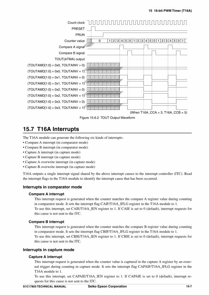
15 16-bit PWM Timer (T16A)
S1C17803 TECHNICAL MANUAL Seiko Epson Corporation 15-7
Count clock
PRESET
PRUN
Counter value
Compare A signal
Compare B signal
TOUT(ATMA) output
(TOUTAMD[1:0] = 0x0, TOUTAINV = 0)
(TOUTAMD[1:0] = 0x0, TOUTAINV = 1)
(TOUTAMD[1:0] = 0x1, TOUTAINV = 0)
(TOUTAMD[1:0] = 0x1, TOUTAINV = 1)
(TOUTAMD[1:0] = 0x2, TOUTAINV = 0)
(TOUTAMD[1:0] = 0x2, TOUTAINV = 1)
(TOUTAMD[1:0] = 0x3, TOUTAINV = 0)
(TOUTAMD[1:0] = 0x3, TOUTAINV = 1)
1 2 3 4 5 00 1 2 3 4 5 0 1 2 3 4 5 0 1
(When T16A_CCA = 3, T16A_CCB = 5)
Figure 15.6.2 TOUT Output Waveform
15.7 T16A InterruptsThe T16A module can generate the following six kinds of interrupts:• Compare A interrupt (in comparator mode)• Compare B interrupt (in comparator mode)• Capture A interrupt (in capture mode) • Capture B interrupt (in capture mode)• Capture A overwrite interrupt (in capture mode)• Capture B overwrite interrupt (in capture mode)
T16A outputs a single interrupt signal shared by the above interrupt causes to the interrupt controller (ITC). Read the interrupt flags in the T16A module to identify the interrupt cause that has been occurred.
Interrupts in comparator mode
Compare A interrupt This interrupt request is generated when the counter matches the compare A register value during counting
in comparator mode. It sets the interrupt flag CAIF/T16A_IFLG register in the T16A module to 1. To use this interrupt, set CAIE/T16A_IEN register to 1. If CAIE is set to 0 (default), interrupt requests for
this cause is not sent to the ITC.
Compare B interrupt This interrupt request is generated when the counter matches the compare B register value during counting
in comparator mode. It sets the interrupt flag CBIF/T16A_IFLG register in the T16A module to 1. To use this interrupt, set CBIE/T16A_IEN register to 1. If CBIE is set to 0 (default), interrupt requests for
this cause is not sent to the ITC.
Interrupts in capture mode
Capture A interrupt This interrupt request is generated when the counter value is captured in the capture A register by an exter-
nal trigger during counting in capture mode. It sets the interrupt flag CAPAIF/T16A_IFLG register in the T16A module to 1.
To use this interrupt, set CAPAIE/T16A_IEN register to 1. If CAPAIE is set to 0 (default), interrupt re-quests for this cause is not sent to the ITC.

15 16-bit PWM Timer (T16A)
15-8 Seiko Epson Corporation S1C17803 TECHNICAL MANUAL
Capture B interrupt This interrupt request is generated when the counter value is captured in the capture B register by an exter-
nal trigger during counting in capture mode. It sets the interrupt flag CAPBIF/T16A_IFLG register in the T16A module to 1.
To use this interrupt, set CAPBIE/T16A_IEN register to 1. If CAPBIE is set to 0 (default), interrupt re-quests for this cause is not sent to the ITC.
Capture A overwrite interrupt This interrupt request is generated if the capture A register is overwritten by a new external trigger when
the capture A interrupt flag CAPAIF has been set (a counter value has already been loaded to the capture A register). It sets the interrupt flag CAPAOWIF/T16A_IFLG register in the T16A module to 1.
To use this interrupt, set CAPAOWIE/T16A_IEN register to 1. If CAPAOWIE is set to 0 (default), interrupt requests for this cause is not sent to the ITC.
CAPAOWIF will be set if the capture A register is overwritten when CAPAIF has been set regardless of whether the capture A register has been read or not. Therefore, be sure to reset CAPAIF immediately after the capture A register is read.
Capture B overwrite interrupt This interrupt request is generated if the capture B register is overwritten by a new external trigger when
the capture B interrupt flag CAPBIF has been set (a counter value has already been loaded to the capture B register). It sets the interrupt flag CAPBOWIF/T16A_IFLG register in the T16A module to 1.
To use this interrupt, set CAPBOWIE/T16A_IEN register to 1. If CAPBOWIE is set to 0 (default), interrupt requests for this cause is not sent to the ITC.
CAPBOWIF will be set if the capture B register is overwritten when CAPBIF has been set regardless of whether the capture B register has been read or not. Therefore, be sure to reset CAPBIF immediately after the capture B register is read.
If the interrupt flag is set to 1 when the interrupt has been enabled, the T16A module outputs an interrupt request to the ITC. An interrupt is generated if the ITC and S1C17 core interrupt conditions are satisfied.For more information on interrupt control registers and the operation when an interrupt occurs, see the “Interrupt Controller (ITC)” chapter.
Notes: • Reset the interrupt flag before enabling interrupts with the interrupt enable bit to prevent oc-currence of unwanted interrupt. The interrupt flag is reset by writing 1.
• After an interrupt occurs, the interrupt flag in the T16A module must be reset in the interrupt handler routine.
15.8 Control Register DetailsTable 15.8.1 List of 16-bit PWM Timer Register
Address Register name Function0x81300 T16A_CTL T16A Counter Control Register Controls the counter.0x81302 T16A_TC T16A Counter Data Register Counter data0x81304 T16A_CCCTL T16A Comparator/Capture Control Register Controls the comparator/capture block and TOUT. 0x81306 T16A_CCA T16A Compare/Capture A Data Register Compare A/capture A data0x81308 T16A_CCB T16A Compare/Capture B Data Register Compare B/capture B data0x8130a T16A_IEN T16A Compare/Capture Interrupt Enable Register Enables/disables interrupts.0x8130c T16A_IFLG T16A Compare/Capture Interrupt Flag Register Displays/sets interrupt occurrence status.
The 16-bit PWM timer registers are described in detail below. These are 16-bit registers.
Note: When data is written to the registers, the “Reserved” bits must always be written as 0 and not 1.

15 16-bit PWM Timer (T16A)
S1C17803 TECHNICAL MANUAL Seiko Epson Corporation 15-9
T16A Counter Control Register (T16A_CTL)Register name Address Bit Name Function Setting Init. R/W Remarks
T16A Counter Control Register(T16A_CTL)
0x81300(16 bits)
D15–12 – reserved – – – 0 when being read.D11–8 CLKS[3:0] Counter clock select CLKS[3:0] Clock 0x0 R/W
0xf0xe0xd0xc0xb0xa0x90x80x70x60x50x40x30x20x10x0
External clockPCLK1•1/16384PCLK1•1/8192PCLK1•1/4096PCLK1•1/2048PCLK1•1/1024PCLK1•1/512PCLK1•1/256PCLK1•1/128PCLK1•1/64PCLK1•1/32PCLK1•1/16PCLK1•1/8PCLK1•1/4PCLK1•1/2PCLK1•1/1
D7–4 – reserved – – – 0 when being read.D3 CBUFEN Compare buffer enable 1 Enable 0 Disable 0 R/WD2 TMMD Count mode select 1 One-shot 0 Repeat 0 R/WD1 PRESET Counter reset 1 Reset 0 Ignored 0 W 0 when being read.D0 PRUN Counter run/stop control 1 Run 0 Stop 0 R/W
D[15:12] Reserved
D[11:8] CLKS[3:0]: Counter Clock Select Bits Selects the counter clock from the 15 different prescaler output clocks and an external clock (EXCL1
input clock).
Table 15.8.2 Counter Clock Selection CLKS[3:0] Clock CLKS[3:0] Clock
0xf External clock 0x7 PCLK1•1/1280xe PCLK1•1/16384 0x6 PCLK1•1/640xd PCLK1•1/8192 0x5 PCLK1•1/320xc PCLK1•1/4096 0x4 PCLK1•1/160xb PCLK1•1/2048 0x3 PCLK1•1/80xa PCLK1•1/1024 0x2 PCLK1•1/40x9 PCLK1•1/512 0x1 PCLK1•1/20x8 PCLK1•1/256 0x0 PCLK1•1/1
(Default: 0x0)
Notes: • Make sure the counter is halted before setting the count clock.
• When using an external clock, the external clock cycle must be at least two CPU operating clock cycles.
D[7:4] Reserved
D3 CBUFEN: Compare Buffer Enable Bit Enables or disables writing to the compare buffer. 1 (R/W): Enabled 0 (R/W): Disabled (default)
When CBUFEN is set to 1, compare data is read and written via the compare data buffer. The buffer contents are loaded into the compare A and compare B registers by the compare B signal.
When CBUFEN is set to 0, compare data is read and written directly from/to the compare A and com-pare B registers.
D2 TMMD: Count Mode Select Bit Selects the count mode. 1 (R/W): One-shot mode 0 (R/W): Repeat mode (default)
Setting TMMD to 0 sets the counter to repeat mode. In this mode, once the count starts, the counter continues counting until stopped by the application program.

15 16-bit PWM Timer (T16A)
15-10 Seiko Epson Corporation S1C17803 TECHNICAL MANUAL
Setting TMMD to 1 sets the counter to one-shot mode. In this mode, the counter stops counting auto-matically as soon as the counter is reset by the compare B signal as well as stopped via software.
D1 PRESET: Counter Reset Bit Resets the counter. 1 (W): Reset 0 (W): Ignored 0 (R): Normally 0 when read out (default)
Writing 1 to this bit resets the counter to 0.
D0 PRUN: Counter Run/Stop Control Bit Starts/stops the count. 1 (W): Run 0 (W): Stop 1 (R): Counting 0 (R): Stopped (default)
The counter starts counting when PRUN is written as 1 and stops when written as 0. The counter data is retained even if the counter is stopped.
T16A Counter Data Register (T16A_TC)Register name Address Bit Name Function Setting Init. R/W Remarks
T16A Counter Data Register(T16A_TC)
0x81302(16 bits)
D15–0 T16ATC[15:0]
Counter dataT16ATC15 = MSBT16ATC0 = LSB
0x0 to 0xffff 0x0 R
D[15:0] T16ATC[15:0]: Counter Data Bits Counter data can be read out. (Default: 0x0) The counter value can be read out even if the counter is running. However, the counter value should be
read at once using a 16-bit transfer instruction. If data is read twice using an 8-bit transfer instruction, the correct value may not be obtained due to occurrence of count up between readings.
T16A Comparator/Capture Control Register (T16A_CCCTL)Register name Address Bit Name Function Setting Init. R/W Remarks
T16A Comparator/Capture Control Register(T16A_CCCTL)
0x81304(16 bits)
D15–14 CAPBTRG[1:0]
Capture B trigger select CAPBTRG[1:0] Trigger edge 0x0 R/W0x30x20x10x0
↑ and ↓↓↑
NoneD13–12 TOUTBMD
[1:0]TOUT B mode select TOUTBMD[1:0] Mode 0x0 R/W
0x30x20x10x0
cmp B: ↑ or ↓cmp A: ↑ or ↓cmp A: ↑, B: ↓
OffD11–10 – reserved – – – 0 when being read.
D9 TOUTBINV TOUT B invert 1 Invert 0 Normal 0 R/WD8 CCBMD T16A_CCB register mode select 1 Capture 0 Comparator 0 R/W
D7–6 CAPATRG[1:0]
Capture A trigger select CAPATRG[1:0] Trigger edge 0x0 R/W0x30x20x10x0
↑ and ↓↓↑
NoneD5–4 TOUTAMD
[1:0]TOUT A mode select TOUTAMD[1:0] Mode 0x0 R/W
0x30x20x10x0
cmp B: ↑ or ↓cmp A: ↑ or ↓cmp A: ↑, B: ↓
OffD3–2 – reserved – – – 0 when being read.
D1 TOUTAINV TOUT A invert 1 Invert 0 Normal 0 R/WD0 CCAMD T16A_CCA register mode select 1 Capture 0 Comparator 0 R/W
D[15:14] CAPBTRG[1:0]: Capture B Trigger Select Bits Selects the trigger edge(s) of the external signal (ATMB input) at which the counter value is captured in
the capture B register.

15 16-bit PWM Timer (T16A)
S1C17803 TECHNICAL MANUAL Seiko Epson Corporation 15-11
Table 15.8.3 Capture B Trigger Edge SelectionCAPBTRG[1:0] Trigger edge
0x3 Falling edge and rising edge 0x2 Falling edge 0x1 Rising edge 0x0 Not triggered
(Default: 0x0)
CAPBTRG[1:0] are control bits for capture mode and are ineffective in comparator mode.
D[13:12] TOUTBMD[1:0]: TOUT B Mode Select Bits Configures how the TOUT B signal waveform (ATMB output) is changed by the compare A and com-
pare B signals. These bits are also used to turn the TOUT B output on and off.
Table 15.8.4 TOUT B Generation Mode TOUTBMD[1:0] When compare A occurs When compare B occurs
0x3 No change Toggle0x2 Toggle No change0x1 Rise Fall0x0 Disable output
(Default: 0x0)
TOUTBMD[1:0] are control bits for comparator mode and are ineffective in capture mode.
D[11:10] Reserved
D9 TOUTBINV: TOUT B Invert Bit Selects the TOUT B signal (ATMB output) polarity. 1 (R/W): Inverted (active low) 0 (R/W): Normal (active high) (default)
Writing 1 to TOUTBINV generates an active low signal (off level = high) for the TOUT B output. When TOUTBINV is 0, an active high signal (off level = low) is generated.
TOUTBINV is a control bit for comparator mode and is ineffective in capture mode.
D8 CCBMD: T16A_CCB Register Mode Select Bit Selects the T16A_CCB register function (comparator mode or capture mode). 1 (R/W): Capture mode 0 (R/W): Comparator mode (default)
Writing 1 to CCBMD configures the T16A_CCB register as the capture B register (capture mode) to which the counter data will be loaded by the external trigger signal. When CCBMD is 0, the T16A_CCB register functions as the compare B register (comparator mode) for writing a comparison value to generate the compare B signal.
D[7:6] CAPATRG[1:0]: Capture A Trigger Select Bits Selects the trigger edge(s) of the external signal (ATMA input) at which the counter value is captured in
the capture A register.
Table 15.8.5 Capture A Trigger Edge SelectionCAPATRG[1:0] Trigger edge
0x3 Falling edge and rising edge 0x2 Falling edge 0x1 Rising edge 0x0 Not triggered
(Default: 0x0)
CAPATRG[1:0] are control bits for capture mode and are ineffective in comparator mode.
D[5:4] TOUTAMD[1:0]: TOUT A Mode Select Bits Configures how the TOUT A signal waveform (ATMA output) is changed by the compare A and com-
pare B signals. These bits are also used to turn the TOUT A output on and off.

15 16-bit PWM Timer (T16A)
15-12 Seiko Epson Corporation S1C17803 TECHNICAL MANUAL
Table 15.8.6 TOUT A Generation Mode TOUTAMD[1:0] When compare A occurs When compare B occurs
0x3 No change Toggle0x2 Toggle No change0x1 Rise Fall0x0 Disable output
(Default: 0x0)
TOUTAMD[1:0] are control bits for comparator mode and are ineffective in capture mode.
D[3:2] Reserved
D1 TOUTAINV: TOUT A Invert Bit Selects the TOUT A signal (ATMA output) polarity. 1 (R/W): Inverted (active low) 0 (R/W): Normal (active high) (default)
Writing 1 to TOUTAINV generates an active low signal (off level = high) for the TOUT A output. When TOUTAINV is 0, an active high signal (off level = low) is generated.
TOUTAINV is a control bit for comparator mode and is ineffective in capture mode.
D0 CCAMD: T16A_CCA Register Mode Select Bit Selects the T16A_CCA register function (comparator mode or capture mode). 1 (R/W): Capture mode 0 (R/W): Comparator mode (default)
Writing 1 to CCAMD configures the T16A_CCA register as the capture A register (capture mode) to which the counter data will be loaded by the external trigger signal. When CCAMD is 0, the T16A_CCA register functions as the compare A register (comparator mode) for writing a comparison value to generate the compare A signal.
T16A Comparator/Capture A Data Register (T16A_CCA)Register name Address Bit Name Function Setting Init. R/W Remarks
T16A Comparator/Capture A Data Register(T16A_CCA)
0x81306(16 bits)
D15–0 CCA[15:0] Compare/capture A dataCCA15 = MSBCCA0 = LSB
0x0 to 0xffff 0x0 R/W
D[15:0] CCA[15:0]: Compare/Capture A Data Bits
In comparator mode (CCAMD/ T16A_CCCTL register = 0) Sets a compare A data, which will be compared with the counter value, through this register. When CBUFEN/T16A_CTL register is set to 0, accessing to this register directly read/write from/to the
compare A register. When CBUFEN is set to 1, accessing to this register read/write from/to the compare A buffer. The buf-
fer contents are loaded into the compare A register when the counter is reset by the compare B signal. The data set is compared with the counter data. When the counter reaches the comparison value set, the
compare A signal is asserted and a cause of compare A interrupt occurs. Furthermore, the TOUT output waveform changes when TOUTAMD[1:0]/T16A_CCCTL register or TOUTBMD[1:0]/T16A_CCCTL register is set to 0x2 or 0x1. These processes do not affect the counter data and the count up operation.
In capture mode (CCAMD = 1) When the counter value is captured at the external trigger signal (ATMA input) edge selected using
CAPATRG[1:0]/T16A_CCCTL register, the captured value is loaded to this register. At the same time a capture A interrupt can be generated, thus the captured counter value can be read out in the interrupt handler.
15 16-bit PWM Timer (T16A)
S1C17803 TECHNICAL MANUAL Seiko Epson Corporation 15-13
T16A Comparator/Capture B Data Register (T16A_CCB)Register name Address Bit Name Function Setting Init. R/W Remarks
T16A Comparator/Capture B Data Register(T16A_CCB)
0x81308(16 bits)
D15–0 CCB[15:0] Compare/capture B dataCCB15 = MSBCCB0 = LSB
0x0 to 0xffff 0x0 R/W
D[15:0] CCB[15:0]: Compare/Capture B Data Bits
In comparator mode (CCBMD/ T16A_CCCTL register = 0) Sets a compare B data, which will be compared with the counter value, through this register. When CBUFEN/T16A_CTL register is set to 0, accessing to this register directly read/write from/to the
compare B register. When CBUFEN is set to 1, accessing to this register read/write from/to the compare B buffer. The buf-
fer contents are loaded into the compare B register when the counter is reset by the compare B signal. The data set is compared with the counter data. When the counter reaches the comparison value set,
the compare B signal is asserted and a cause of compare B interrupt occurs. The counter is reset to 0. Furthermore, the TOUT output waveform changes when TOUTAMD[1:0]/T16A_CCCTL register or TOUTBMD[1:0]/T16A_CCCTL register is set to 0x3 or 0x1. These processes do not affect the counter data and the count up operation.
In capture mode (CCBMD = 1) When the counter value is captured at the external trigger signal (ATMB input) edge selected using
CAPBTRG[1:0]/T16A_CCCTL register, the captured value is loaded to this register. At the same time a capture B interrupt can be generated, thus the captured counter value can be read out in the interrupt handler.
T16A Comparator/Capture Interrupt Enable Register (T16A_IEN)Register name Address Bit Name Function Setting Init. R/W Remarks
T16A Comparator/Capture Interrupt Enable Register(T16A_IEN)
0x8130a(16 bits)
D15–6 – reserved – – – 0 when being read.D5 CAPBOWIE Capture B overwrite interrupt enable 1 Enable 0 Disable 0 R/WD4 CAPAOWIE Capture A overwrite interrupt enable 1 Enable 0 Disable 0 R/WD3 CAPBIE Capture B interrupt enable 1 Enable 0 Disable 0 R/WD2 CAPAIE Capture A interrupt enable 1 Enable 0 Disable 0 R/WD1 CBIE Compare B interrupt enable 1 Enable 0 Disable 0 R/WD0 CAIE Compare A interrupt enable 1 Enable 0 Disable 0 R/W
D[15:6] Reserved
D5 CAPBOWIE: Capture B Overwrite Interrupt Enable Bit Enables or disables capture B overwrite interrupts. 1 (R/W): Interrupt enabled 0 (R/W): Interrupt disabled (default)
Setting CAPBOWIE to 1 enables capture B overwrite interrupt requests to the ITC. Setting it to 0 dis-ables interrupts.
D4 CAPAOWIE: Capture A Overwrite Interrupt Enable Bit Enables or disables capture A overwrite interrupts. 1 (R/W): Interrupt enabled 0 (R/W): Interrupt disabled (default)
Setting CAPAOWIE to 1 enables capture A overwrite interrupt requests to the ITC. Setting it to 0 dis-ables interrupts.
D3 CAPBIE: Capture B Interrupt Enable Bit Enables or disables capture B interrupts. 1 (R/W): Interrupt enabled 0 (R/W): Interrupt disabled (default)
Setting CAPBIE to 1 enables capture B interrupt requests to the ITC. Setting it to 0 disables interrupts.

15 16-bit PWM Timer (T16A)
15-14 Seiko Epson Corporation S1C17803 TECHNICAL MANUAL
D2 CAPAIE: Capture A Interrupt Enable Bit Enables or disables capture A interrupts. 1 (R/W): Interrupt enabled 0 (R/W): Interrupt disabled (default)
Setting CAPAIE to 1 enables capture A interrupt requests to the ITC. Setting it to 0 disables interrupts.
D1 CBIE: Compare B Interrupt Enable Bit Enables or disables compare B interrupts. 1 (R/W): Interrupt enabled 0 (R/W): Interrupt disabled (default)
Setting CBIE to 1 enables compare B interrupt requests to the ITC. Setting it to 0 disables interrupts.
D0 CAIE: Compare A Interrupt Enable Bit Enables or disables compare A interrupts. 1 (R/W): Interrupt enabled 0 (R/W): Interrupt disabled (default)
Setting CAIE to 1 enables compare A interrupt requests to the ITC. Setting it to 0 disables interrupts.
T16A Comparator/Capture Interrupt Flag Register (T16A_IFLG)Register name Address Bit Name Function Setting Init. R/W Remarks
T16A Comparator/Capture Interrupt Flag Register(T16A_IFLG)
0x8130c(16 bits)
D15–6 – reserved – – – 0 when being read.D5 CAPBOWIF Capture B overwrite interrupt flag 1 Cause of
interrupt occurred
0 Cause of interrupt not occurred
0 R/W Reset by writing 1.D4 CAPAOWIF Capture A overwrite interrupt flag 0 R/WD3 CAPBIF Capture B interrupt flag 0 R/WD2 CAPAIF Capture A interrupt flag 0 R/WD1 CBIF Compare B interrupt flag 0 R/WD0 CAIF Compare A interrupt flag 0 R/W
D[15:6] Reserved
D5 CAPBOWIF: Capture B Overwrite Interrupt Flag Bit Indicates whether the cause of capture B overwrite interrupt has occurred or not. 1 (R): Cause of interrupt has occurred 0 (R): No cause of interrupt has occurred (default) 1 (W): Flag is reset 0 (W): Ignored
CAPBOWIF is a T16A interrupt flag that is set to 1 when the capture B register is overwritten. CAPBOWIF is reset by writing 1.
D4 CAPAOWIF: Capture A Overwrite Interrupt Flag Bit Indicates whether the cause of capture A overwrite interrupt has occurred or not. 1 (R): Cause of interrupt has occurred 0 (R): No cause of interrupt has occurred (default) 1 (W): Flag is reset 0 (W): Ignored
CAPAOWIF is a T16A interrupt flag that is set to 1 when the capture A register is overwritten. CAPAOWIF is reset by writing 1.
D3 CAPBIF: Capture B Interrupt Flag Bit Indicates whether the cause of capture B interrupt has occurred or not. 1 (R): Cause of interrupt has occurred 0 (R): No cause of interrupt has occurred (default) 1 (W): Flag is reset 0 (W): Ignored
CAPBIF is a T16A interrupt flag that is set to 1 when the counter value is captured in the capture B reg-ister.
CAPBIF is reset by writing 1.

15 16-bit PWM Timer (T16A)
S1C17803 TECHNICAL MANUAL Seiko Epson Corporation 15-15
D2 CAPAIF: Capture A Interrupt Flag Bit Indicates whether the cause of capture A interrupt has occurred or not. 1 (R): Cause of interrupt has occurred 0 (R): No cause of interrupt has occurred (default) 1 (W): Flag is reset 0 (W): Ignored
CAPAIF is a T16A interrupt flag that is set to 1 when the counter value is captured in the capture A reg-ister.
CAPAIF is reset by writing 1.
D1 CBIF: Compare B Interrupt Flag Bit Indicates whether the cause of compare B interrupt has occurred or not. 1 (R): Cause of interrupt has occurred 0 (R): No cause of interrupt has occurred (default) 1 (W): Flag is reset 0 (W): Ignored
CBIF is a T16A interrupt flag that is set to 1 when the counter reaches the value set in the compare B register.
CBIF is reset by writing 1.
D0 CAIF: Compare A Interrupt Flag Bit Indicates whether the cause of compare A interrupt has occurred or not. 1 (R): Cause of interrupt has occurred 0 (R): No cause of interrupt has occurred (default) 1 (W): Flag is reset 0 (W): Ignored
CAIF is a T16A interrupt flag that is set to 1 when the counter reaches the value set in the compare A register.
CAIF is reset by writing 1.

16 16-bit Audio PWM Timer (T16P)
S1C17803 TECHNICAL MANUAL Seiko Epson Corporation 16-1
16 16-bit Audio PWM Timer (T16P)
16.1 T16P Module OverviewThe S1C17803 incorporate a 16-bit audio PWM timer (T16P) that generates PWM pulses from PCM data. The pulses generated can be directly output to a low pass filter that eliminates quantization noise to shape the output signal into sound waveform. A monophonic audio output system can be implemented simply without an external D/A converter.
16-bit audio PWM timer
PCM data
LPF AMPPWM waveform
S1C17803
Sound waveform
Figure 16.1.1 Audio Output Circuit Using T16P
If no audio output feature is required, T16P can be used as a general-purpose 16-bit timer.The following lists the main functions of T16P.
• Supports 8-bit and 16-bit PCM data with varied sample rates: 8k, 16k, 22.05k, 32k, 44.1k, and 48k.
• Supports both signed and unsigned PCM data.
• Supports split mode; 16-bit audio data can be split into 10 bits + 6 bits, 9 bits + 7 bits, or 8 bits + 8 bits.
• Supports fine mode to improve the precision of the pulse width.
• Includes a digital volume control unit.
• Programmable count clocks using the prescaler or an external clock
• Built-in two 16-bit data buffers for setting pulse widths (duty cycles) and pulse periods
• Can generate three different types of interrupts and invoke a DMA.
Figure 16.1.2 shows the T16P configuration.
16-bit up counter
Compare A register
Compare B register
Volume control unit
Control circuit
Clock control circuit
Prescaler
Comparator
TMHTML
Clock output
To ITC
B match
A match
AH/ALmatch
Interrupt
16-bit Audio PWM Timer
EXCL0
Inte
rnal
dat
a bu
s
Compare A buffer
Comparator
Figure 16.1.2 16-bit Audio PWM Timer Configuration

16 16-bit Audio PWM Timer (T16P)
16-2 Seiko Epson Corporation S1C17803 TECHNICAL MANUAL
T16P consists of a 16-bit up-counter and two 16-bit compare data buffers/registers.The 16-bit counter can be reset to 0 via software and counts up using a prescaler output clock or an external clock input from the EXCL0 pin.The compare A buffer is used to store data (PCM data). The stored data is loaded to the compare A register and compared with the counter value to determine the output pulse width. The volume control unit multiplies the PCM data stored in the compare A buffer by the specified volume level set via software before loading to the compare A register. This makes it possible to adjust the volume level to 1/64 through 127/64 as well as muting.The compare B buffer is used to store data to determine a pulse period. The stored data is loaded to the compare B register and compared with the counter value.When the counter value reaches the compare data, the timer output signal is inverted to generate PWM waveform.
16.2 T16P Input/Output PinsTable 16.2.1 lists the input/output pins for the T16P module.
Table 16.2.1 List of T16P PinsPin name I/O Qty Function
EXCL0 I 1 T16P/WDT external clock input pinInputs an external clock as the count clock.
TMH O 1 PWM signal output pinIn a split mode: Outputs the PWM signal generated from the high-order PCM
data bits.In normal mode: Outputs the PWM signal generated from the PCM data.
TML O 1 PWM signal output pinIn a split mode: Outputs the PWM signal generated from the low-order PCM data
bits.In normal mode: Fixed at the initial output level (or not used).
The T16P input/output pins (EXCL0, TMH, TML) are shared with I/O ports and are initially set as general purpose I/O port pins. The pin functions must be switched using the port function select bits to use the general purpose I/O port pins as T16P input/output pins.For detailed information on pin function switching, see the “I/O Ports (GPIO)” chapter.
16.3 Setting T16P Operating ConditionsMake the following settings before starting T16P.1. Configure the T16P input/output pins. (See Section 16.2.)2. Select the count clock. (See Section 16.3.1.) 3. Configure the PCM data (resolution, signed/unsigned data format). (See Section 16.3.2.)4. Select the operating modes (split mode, fine mode). (See Section 16.3.3.)5. Set the PWM output condition (initial signal level). (See Section 16.3.4.)6. Set interrupt and/or DMA conditions. (See Section 16.5.)
16.3.1 Count Clock
Either an internal clock or an external clock can be selected as the count clock using CLKSEL/T16P_CTL register. When CLKSEL is set to 0 (default), an internal clock is used; when set to 1, the external clock input to the EXCL0 pin is used.When using an external clock, the external clock cycle must be at least two CPU operating clock cycles.When an internal clock is used, it can be selected using CLKDIV[3:0]/T16P_CLK register from the 13 types gener-ated by the prescaler (PSC Ch.1) dividing the PCLK1 clock into 1/1 to 1/4,096.

16 16-bit Audio PWM Timer (T16P)
S1C17803 TECHNICAL MANUAL Seiko Epson Corporation 16-3
Table 16.3.1.1 Internal Clock SelectionCLKDIV[3:0] Count clock CLKDIV[3:0] Count clock
0xf Reserved 0x7 PCLK1•1/1280xe Reserved 0x6 PCLK1•1/640xd Reserved 0x5 PCLK1•1/320xc PCLK1•1/4096 0x4 PCLK1•1/160xb PCLK1•1/2048 0x3 PCLK1•1/80xa PCLK1•1/1024 0x2 PCLK1•1/40x9 PCLK1•1/512 0x1 PCLK1•1/20x8 PCLK1•1/256 0x0 PCLK1•1/1
(Default: 0x0)
Note: Make sure the counter is halted before setting the count clock.
For controlling PSC Ch.1, refer to the “Prescaler (PSC)” chapter.
16.3.2 PCM Data Configuration
The resolution and data format must be specified for manipulating PCM data.
Data resolution T16P supports 8-bit and 16-bit PCM data. Use RESSEL/T16P_CTL register to select the resolution. When
RESSEL is set to 1 (default), 16-bit resolution is selected; when set to 0, 8-bit resolution is selected.
Data format T16P supports signed and unsigned PCM data. Use SGNSEL/T16P_CTL register to select the data format.
When SGNSEL is set to 1 (default), signed data format is selected; when set to 0, unsigned data format is se-lected.
16.3.3 Operating Mode Selection
Split mode When 16-bit PCM data is used, it can be manipulated by splitting into two data units. Use SPLTMD[1:0]/
T16P_CTL register to select a split mode.
Table 16.3.3.1 Split Mode SelectionSPLTMD[1:0] Split mode
0x3 10 bits + 6 bits split mode0x2 9 bits + 7 bits split mode0x1 8 bits + 8 bits split mode0x0 16 bits normal mode
(Default: 0x0) When a split mode is selected, the split high-order bits (10, 9, or 8 high-order bits) of the compare A data and
the low-order bits (6, 7, or 8 low-order bits) are compared with the counter data and the two comparison results generate two PWM output signals. The PWM signal generated from the high-order data bits is output from the TMH pin and another generated from the low-order data bits is output from the TML pin. When a split mode or 8-bit PCM data resolution is selected, compare A interrupts cannot be generated.
Outputclock
generator
High-order bits
TMH output
TML output
AH match
Compare A register
16-bit up counter
Low-order bits
Counter[15:0]
AL match
Figure 16.3.3.1 Split Mode

16 16-bit Audio PWM Timer (T16P)
16-4 Seiko Epson Corporation S1C17803 TECHNICAL MANUAL
When normal mode is selected (SPLTMD[1:0] = 0x0), 16-bit PCM (compare A) data is compared with the 16-bit counter data and the PWM signal generated is output from the TMH pin. If TML output function is en-abled, the TML pin is fixed at the initial output level. If this mode and 16-bit PCM data resolution are selected, compare A interrupts can be generated when the counter reaches the compare A data.
Fine mode Normally, compare A data is compared with the counter data at the rising edge of the count clock. When T16P
is set to fine mode, the comparisons are performed at both rising and falling edges of the count clock. At this time the compare A data is halved when compared.
Count clock (PCLK1)
Counter
TMH output in normal comparison mode
TMH output in fine mode
(Compare A data = 3, Compare B data = 5)
1 2 3 4 5 00 1 2 3 4 5 0 1
Figure 16.3.3.2 Fine Mode
The fine mode improves the precision of the pulse width. Note, however, that the PCLK1•1/1 clock can only be used as the count clock in this mode. CLKSEL and CLKDIV[3:0] settings are ineffective.
Set SELFM/T16P_CTL to 1 to set T16P to fine mode. The fine mode does not affect the pulse period that is determined with compare B data.
16.3.4 PWM Output Condition Settings
Initial output level The TMH and TML PWM output pins go to the initial output level when the pin function is switched for T16P
before starting T16P or when T16P is stopped or reset. Use INITOL/T16P_CTL register to select the initial out-put level.
When INITOL is 0 (default), the initial output level is low. When INITOL is set to 1, the initial output level is set to high.
Note: Before the pin function is switched for T16P, be sure to set INITOL and then reset the PWM (set PRESET to 1).
16.4 Control and T16P Operations
16.4.1 Resetting T16P
Writing 1 to PRESET/T16P_CTL register resets T16P. The following operations are performed when PRESET is set to 1.• The counter (CNT_DATA[15:0]/T16P_CNT_DATA register) is reset to 0x0.• The compare B counter (BCNT[3:0]/T16P_CTL register) is reset to 0x0.• The compare A and B buffers/registers (CMPA[15:0]/T16P_A register, CMPB[15:0]/T16P_B register) are reset
to 0x0.• The buffer empty flag (BUFEF/T16P_INT register) is set to 1. (No interrupt occurs.)• All other interrupt flags are reset to 0 and interrupt requests are canceled.• DMA request is canceled if it has been issued.• The PWM outputs go to the initial output level set by INITOL/T16P_CTL register.
Note: Be sure to reset T16P before the GPIO pins are switched to the TMH and TML pins, and before setting PRUN/T16P_RUN register to 1 to start T16P.

16 16-bit Audio PWM Timer (T16P)
S1C17803 TECHNICAL MANUAL Seiko Epson Corporation 16-5
16.4.2 Run/Stop Control
To start T16P, write 1 to PRUN/T16P_RUN register.T16P must be reset (write 1 to PRESET/T16P_CTL register) before writing 1 to PRUN. Resetting the T16P sets the buffer empty flag to 1, but neither an interrupt request nor a DMA request is issued at this point even if the buffer empty interrupt is enabled. Writing 1 to PRUN enables T16P to issue buffer empty interrupts and DMA requests, so that the first audio data can be sent to the buffer in the interrupt handler routine or DMA.To stop T16P being run, write 0 to PRUN. Note that T16P may not stop counting until B match conditions occur (BCNT[3:0] + 1) times.
16.4.3 Setting Compare Data
Compare A buffer The compare A buffer (CMPA[15:0]/T16P_A register) is used to specify output pulse widths (duty cycles). Set
output audio data to this buffer. The buffer data is loaded to the compare A register when the timer starts count-ing or when a B match occurs specified number of times, and is compared with the counter value. The output signal level is inverted at the beginning of a pulse period and when the counter reaches the compare data stored in the compare A register. This operation converts audio data set to the compare A buffer into a pulse width.
When the data written to the compare A buffer is loaded to the compare A register, the buffer empty interrupt flag (BUFEF/T16P_INT register) is set to 1 and an interrupt occurs if buffer empty interrupts are enabled. Also this cause of interrupt can invoke a DMA transfer. By using this interrupt or DMA transfer, the next output data can be set to the compare A buffer.
When the counter reaches the compare A data, the A match interrupt flag (INTAF/T16P_INT register) is set to 1 and an interrupt occurs if A match interrupts are enabled. This type of interrupts does not occur in split mode or when 8-bit PCM data resolution is selected.
The pulse width set by compare A data is as follows:
In normal comparison mode (SELFM = 0) Output pulse width = CMPA × Count clock cycle
(CMPA: CMPA[15:0] in normal mode, CMPA[15:n] or CMPA[(n-1):0] in split mode)
In fine mode (SELFM = 1) Output pulse width = CMPA × PCLK1 cycle × 1/2
(CMPA: CMPA[15:0] in normal mode, CMPA[15:n] or CMPA[(n-1):0] in split mode)
An 8-bit audio data should be written to CMPA[7:0].
Compare B buffer and B match counter The compare B buffer (CMPB[15:0]/T16P_B register) is used to specify pulse periods. The buffer data is load-
ed to the compare B register and is compared with the counter value. The output signal level is inverted when the counter reaches the compare data stored in the compare B register (B match). When a B match occurs the counter is reset to 0x0 to start the next pulse period. This operation generates a pulse period according to the compare B data specified.
When the counter reaches the compare B data, the B match interrupt flag (INTBF/T16P_INT register) is set to 1 and an interrupt occurs if B match interrupts are enabled.
The T16P controller includes the B match counter (BCNT[3:0]/T16P_CTL register) to set the sampling rate. Set BCNT[3:0] to 0 to 15. When a B match occurs (BCNT[3:0] + 1) times, the compare A and B buffer data are loaded into the compare A and B registers to start new sampling period.
The pulse period set by compare B data is as follows:
Output pulse period = (CMPB[15:0] + 1) × Count clock cycle
Sampling period = (CMPB[15:0] + 1) × Count clock cycle × (BCNT[3:0] + 1)

16 16-bit Audio PWM Timer (T16P)
16-6 Seiko Epson Corporation S1C17803 TECHNICAL MANUAL
16.4.4 Volume Control
T16P includes a volume control function. To use this function, set VOLBPS/T16P_VOL_CTL to 0. The vol-ume control unit multiplies the PCM data stored in the compare A buffer by the specified volume level set using VOLSEL[6:0]/T16P_VOL_CTL register before loading to the compare A register. This makes it possible to adjust the volume level to 1/64 through 127/64 as well as muting.
Table 16.4.4.1 Volume Level SettingsVOLSEL[6:0] Volume level
0x7f × 127/640x7e × 126/64
:0x40
:
:× 64/64
:0x2 × 2/640x1 × 1/640x0 × 0 (mute)
(Default: 0x40)
When VOLBPS is set to 1 (default), the volume control unit is bypassed and compare A data is directly loaded to the compare A register. When 8-bit PCM data is used, the volume control unit should be bypassed by setting VOLBPS to 1.
16.4.5 Counter Value
The counter data can be read out from CNT_DATA[15:0]/T16P_CNT_DATA register at any time. Counter data can also be written to CNT_DATA[15:0]. This makes it possible to change the interrupt and/or
timer output cycles temporarily.
16.4.6 Timing Charts
Normal modeCount clock
PRESET
PRUN
Compare data load
Compare A register
Compare B register
Counter
A match signal
B match signal
TMH output (INITOL = 0)
TML output (INITOL = 0)
TMH output (INITOL = 1)
TML output (INITOL = 1)
Buffer empty interrupt
A match interrupt
B match interrupt
1 2 3 4 5 00
0 3 4
1 2 3 4 5 0 1 2 3 4 5 0 1
0 5 5
2 3 4 5 0 1
(When BCNT[3:0] = 1)
Figure 16.4.6.1 PWM Output Timing Chart 1 (normal mode)

16 16-bit Audio PWM Timer (T16P)
S1C17803 TECHNICAL MANUAL Seiko Epson Corporation 16-7
Normal + fine modeCount clock (PCLK1)
PRESET
PRUN
Compare data load
Compare A register
Compare B register
Counter
A match signal
B match signal
TMH output (INITOL = 0)
TML output (INITOL = 0)
TMH output (INITOL = 1)
TML output (INITOL = 1)
Buffer empty interrupt
A match interrupt
B match interrupt
1 2 3 4 5 00
0 3 4
1 2 3 4 5 0 1 2 3 4 5 0 1
0 5 5
2 3 4 5 0 1
(When BCNT[3:0] = 1)
Figure 16.4.6.2 PWM Output Timing Chart 2 (normal + fine mode)
Split modeCount clock
PRESET
PRUN
Compare data load
Compare A register
Compare B register
Counter
AH match signal
AL match signal
B match signal
TMH output (INITOL = 0)
TML output (INITOL = 0)
TMH output (INITOL = 1)
TML output (INITOL = 1)
Buffer empty interrupt
A match interrupt
B match interrupt
1 2 3 4 5 00
0 AH = 1, AL = 3 AH = 2, AL = 4
1 2 3 4 5 0 1 2 3 4 5 0 1
0 5 5
2 3 4 5 0 1
(When BCNT[3:0] = 1)
(not occurred)
Figure 16.4.6.3 PWM Output Timing Chart 3 (split mode)

16 16-bit Audio PWM Timer (T16P)
16-8 Seiko Epson Corporation S1C17803 TECHNICAL MANUAL
Split + fine modeCount clock (PCLK1)
PRESET
PRUN
Compare data load
Compare A register
Compare B register
Counter
AH match signal
AL match signal
B match signal
TMH output (INITOL = 0)
TML output (INITOL = 0)
TMH output (INITOL = 1)
TML output (INITOL = 1)
Buffer empty interrupt
A match interrupt
B match interrupt
1 2 3 4 5 00
0 AH = 1, AL = 3 AH = 2, AL = 4
1 2 3 4 5 0 1 2 3 4 5 0 1
0 5 5
2 3 4 5 0 1
(When BCNT[3:0] = 1)
(not occurred)
Figure 16.4.6.4 PWM Output Timing Chart 4 (split + fine mode)
16.5 T16P Interrupts and DMAThis section describes the T16P interrupts and invoking DMA.For more information on interrupt processing and DMA transfer, see the “Interrupt Controller (ITC)” chapter and the “DMA Controller (DMAC)” chapter, respectively.
16.5.1 Interrupts
The T16P module can generate the following three kinds of interrupts:• Buffer empty interrupt• A match interrupt• B match interrupt
T16P outputs a single interrupt signal shared by the above interrupt causes to the interrupt controller (ITC). Read the interrupt flags in the T16P module to identify the interrupt cause that has been occurred.
Buffer empty interrupt This interrupt request is generated when compare A buffer data is loaded into the compare A registers. It sets
the interrupt flag BUFEF/T16P_INT register in the T16P module to 1. To use this interrupt, set INTBEEN/T16P_INT register to 1. If INTBEEN is set to 0 (default), interrupt requests
for this cause is not sent to the ITC.
A match interrupt This interrupt request is generated when the counter reaches the compare A register value during counting. It
sets the interrupt flag INTAF/T16P_INT register in the T16P module to 1. To use this interrupt, set INTAEN/T16P_INT register to 1. If INTAEN is set to 0 (default), interrupt requests for
this cause is not sent to the ITC. When a split mode or 8-bit PCM data resolution is selected, INTAF will not be set and A match interrupts will
not be occurred.

16 16-bit Audio PWM Timer (T16P)
S1C17803 TECHNICAL MANUAL Seiko Epson Corporation 16-9
B match interrupt This interrupt request is generated when the counter reaches the compare B register value during counting. It
sets the interrupt flag INTBF/T16P_INT register in the T16P module to 1. To use this interrupt, set INTBEN/T16P_INT register to 1. If INTBEN is set to 0 (default), interrupt requests
for this cause is not sent to the ITC.
If the interrupt flag is set to 1 when the interrupt has been enabled, the T16P module outputs an interrupt request to the ITC. An interrupt is generated if the ITC and S1C17 core interrupt conditions are satisfied.For more information on interrupt control registers and the operation when an interrupt occurs, see the “Interrupt Controller (ITC)” chapter.
Notes: • Reset the interrupt flag before enabling interrupts with the interrupt enable bit to prevent oc-currence of unwanted interrupt. The interrupt flag is reset by writing 1.
• After an interrupt occurs, the interrupt flag in the T16P module must be reset in the interrupt handler routine.
16.5.2 DMA Transfer
The causes of buffer empty interrupts can invoke a DMA. This allows continuous data transfer via the DMAC be-tween memory and the compare A buffer. The buffer empty interrupt signal is output to both the ITC and DMAC. Therefore, DMA transfer can be performed without generating a T16P interrupt.For more information on DMA transfer, see the “DMA Controller (DMAC)” chapter.
16.6 Control Register Details
Table 16.6.1 List of T16P RegistersAddress Register name Function
0x81400 T16P_A T16P Compare A Buffer Register Compare A data0x81402 T16P_B T16P Compare B Buffer Register Compare B data0x81404 T16P_CNT_DATA T16P Counter Data Register Counter data
0x81406 T16P_VOL_CTL T16P Volume Control Register Enables the volume control and sets a volume level.0x81408 T16P_CTL T16P Control Register Sets the timer operating conditions.0x8140a T16P_RUN T16P Running Control Register Starts/stops the timer.0x8140c T16P_CLK T16P Internal Clock Control Register Selects an internal count clock.0x8140e T16P_INT T16P Interrupt Control Register Controls T16P interrupts.
The T16P registers are described in detail below. These are 16-bit registers.
Note: When data is written to the registers, the “Reserved” bits must always be written as 0 and not 1.
T16P Compare A Buffer Register (T16P_A)Register name Address Bit Name Function Setting Init. R/W Remarks
T16P Compare A Buffer Register(T16P_A)
0x81400(16 bits)
D15–0 CMPA[15:0] Compare A dataCMPA15 = MSBCMPA0 = LSB
0x0 to 0xffff X R/W
D[15:0] CMPA[15:0]: Compare A Data Bits Sets compare A data (PCM data) to be converted to a pulse width. (Default: undefined) The buffer data is loaded to the compare A register when the timer starts counting or when a B match
occurs specified number of times, and is compared with the counter value. The output signal level is inverted at the beginning of a pulse period and when the counter reaches the compare data stored in the compare A register. This operation converts audio data set to the compare A buffer into a pulse width.
When the data written to the compare A buffer is loaded to the compare A register, the buffer empty interrupt flag (BUFEF/T16P_INT register) is set to 1 and an interrupt occurs if buffer empty interrupts are enabled. Also this cause of interrupt can invoke a DMA transfer. By using this interrupt or DMA transfer, the next output data can be set to the compare A buffer.

16 16-bit Audio PWM Timer (T16P)
16-10 Seiko Epson Corporation S1C17803 TECHNICAL MANUAL
When the counter reaches the compare A data, the A match interrupt flag (INTAF/T16P_INT register) is set to 1 and an interrupt occurs if A match interrupts are enabled. This type of interrupts does not oc-cur in split mode or when 8-bit PCM data resolution is selected.
The pulse width set by compare A data is as follows:
In normal comparison mode (SELFM/T16P_CTL register = 0) Output pulse width = CMPA × Count clock cycle
(CMPA: CMPA[15:0] in normal mode, CMPA[15:n] or CMPA[(n-1):0] in split mode)
In fine mode (SELFM = 1) Output pulse width = CMPA × PCLK1 cycle × 1/2
(CMPA: CMPA[15:0] in normal mode, CMPA[15:n] or CMPA[(n-1):0] in split mode)
16-bit audio data must be written to CMPA[15:0] (address 0x81400) in 16-bit size. 8-bit audio data should be written to CMPA[15:8] (address 0x81401) in 8-bit units.
When signed data format is selected, CMPA15 is treated as the sign bit for both 16-bit and 8-bit audio data.
T16P Compare B Buffer Register (T16P_B)Register name Address Bit Name Function Setting Init. R/W Remarks
T16P Compare B Buffer Register(T16P_B)
0x81402(16 bits)
D15–0 CMPB[15:0] Compare B dataCMPB15 = MSBCMPB0 = LSB
0x0 to 0xffff X R/W
D[15:0] CMPB[15:0]: Compare B Data Bits Sets compare B data to be converted to a pulse period. (Default: undefined) The buffer data is loaded to the compare B register and is compared with the counter value. The output
signal level is inverted when the counter reaches the compare data stored in the compare B register (B match). When a B match occurs the counter is reset to 0x0 to start the next pulse period. This operation generates a pulse period according to the compare B data specified.
When the counter reaches the compare B data, the B match interrupt flag (INTBF/T16P_INT register) is set to 1 and an interrupt occurs if B match interrupts are enabled.
When a B match occurs the number of times (BCNT[3:0] + 1), the compare A and B buffer data are loaded into the compare A and B registers to start new sampling period.
The pulse period set by compare B data is as follows:
Output pulse period = (CMPB[15:0] + 1) × Count clock cycle
Sampling period = (CMPB[15:0] + 1) × Count clock cycle × (BCNT[3:0] + 1)
T16P Counter Data Register (T16P_CNT_DATA)Register name Address Bit Name Function Setting Init. R/W Remarks
T16P Counter Data Register(T16P_CNT_DATA)
0x81404(16 bits)
D15–0 CNT_DATA[15:0]
Counter dataCNT_DATA15 = MSBCNT_DATA0 = LSB
0x0 to 0xffff X R/W
D[15:0] CNT_DATA[15:0]: Counter Data Bits The counter data can be read from this register. (Default: undefined) Furthermore, data can be set to the counter by writing it to this register. The counter is reset to 0x0 when a B match occurs or when T16P is reset by setting PRESET/T16P_
CTL to 1.

16 16-bit Audio PWM Timer (T16P)
S1C17803 TECHNICAL MANUAL Seiko Epson Corporation 16-11
T16P Volume Control Register (T16P_VOL_CTL)Register name Address Bit Name Function Setting Init. R/W Remarks
T16P Volume Control Register(T16P_VOL_CTL)
0x81406(16 bits)
D15–8 – reserved – – – 0 when being read.D7 VOLBPS Volume control enable 1 Disable 0 Enable 1 R/W Effective only for 16-
bit dataD6–0 VOLSEL[6:0]
Volume level select VOLSEL[6:0] Volume level 0x40 R/W0x7f0x7e
:0x40
:0x20x10x0
× 127/64× 126/64
:× 64/64
:× 2/64× 1/64
× 0 (mute)
D[15:8] Reserved
D7 VOLBPS: Volume Control Enable Bit Enables or disables the volume control function. 1 (R/W): Disabled (bypassed) (default) 0 (R/W): Enabled
When VOLBPS is set to 0, the volume control unit multiplies the PCM data stored in the compare A buffer by the specified volume level set using VOLSEL[6:0] before loading to the compare A register.
If no volume control is required, set VOLBPS to 0.
Note: When 8-bit PCM data is used, the volume control unit should be bypassed by setting VOLBPS to 1.
D[6:0] VOLSEL[6:0]: Volume Level Select Bits Selects a volume level when the volume control function is enabled.
Table 16.6.2 Volume Level SettingsVOLSEL[6:0] Volume level
0x7f × 127/640x7e × 126/64
:0x40
:
:× 64/64
:0x2 × 2/640x1 × 1/640x0 × 0 (mute)
(Default: 0x40)
T16P Control Register (T16P_CTL)Register name Address Bit Name Function Setting Init. R/W Remarks
T16P Control Register(T16P_CTL)
0x81408(16 bits)
D15–12 BCNT[3:0] B match count 0x0 to 0xf 0x0 R/WD11 RESSEL PCM data resolution select 1 16 bits 0 8 bits 1 R/WD10 SGNSEL PCM data format select 1 Signed 0 Unsigned 1 R/W
D9–8 SPLTMD[1:0]
Split mode select SPLTMD[1:0] Split mode 0x0 R/W Effective only for 16-bit data0x3
0x20x10x0
10 bits + 6 bits9 bits + 7 bits8 bits + 8 bits
Normal (16 bits)D7 – reserved – – – 0 when being read.D6 SELFM Fine mode select 1 Fine mode 0 Normal 0 R/WD5 – reserved – – – 0 when being read.D4 INITOL Initial output level select 1 High 0 Low 0 R/WD3 CLKSEL Input clock select 1 External 0 Internal 0 R/WD2 – reserved – – – 0 when being read.D1 PRESET T16P reset 1 Reset 0 Ignored 0 WD0 – reserved – – –
D[15:12] BCNT[3:0]: B Match Count Bits Sets the B match counter. (Default: 0x0) When a B match occurs (BCNT[3:0] + 1) times, the compare A and B buffer data are loaded into the
compare A and B registers.

16 16-bit Audio PWM Timer (T16P)
16-12 Seiko Epson Corporation S1C17803 TECHNICAL MANUAL
D11 RESSEL: PCM Data Resolution Select Bit Selects the PCM data resolution. 1 (R/W): 16 bits (default) 0 (R/W): 8 bits
When 8-bit PCM data is used, 8 bits + 8 bits split mode must be selected and audio data should be writ-ten to CMPA[15:8] (address 0x81401) in 8-bit size. The PWM pulses will be output from the TMH pin and the TML pin is fixed at the level set by INITOL.
Note: When 8-bit PCM data resolution is selected, no A match interrupt will be generated.
D10 SGNSEL: PCM Data Format Select Bit Selects the PCM data format. 1 (R/W): Signed data (default) 0 (R/W): Unsigned data
D[9:8] SPLTMD[1:0]: Split Mode Select Bits Selects the split mode for manipulating 16-bit PCM data.
Table 16.6.3 Split Mode SelectionSPLTMD[1:0] Split mode
0x3 10 bits + 6 bits split mode0x2 9 bits + 7 bits split mode0x1 8 bits + 8 bits split mode0x0 16 bits normal mode
(Default: 0x0)
When a split mode is selected, the split high-order data bits (10, 9, or 8 high-order bits) and low-order data bits (6, 7, or 8 low-order bits) are compared with the counter data and the two comparison results generate two PWM output signals. The PWM signal generated from the high-order data bits is output from the TMH pin and another generated from the low-order data bits is output from the TML pin. When a split mode or 8-bit PCM data resolution is selected, compare A interrupts cannot be generated.
Note: SPLTMD[1:0] does not affect 8-bit PCM data.
D7 Reserved
D6 SELFM: Fine Mode Select Bit Sets T16P to fine mode. 1 (R/W): Fine mode 0 (R/W): Normal comparison mode (default)
In normal comparison mode, compare A data is compared with the counter data at the rising edge of the count clock. When T16P is set to fine mode, the comparisons are performed at both rising and falling edges of the count clock. At this time the compare A data is halved when compared.
Count clock (PCLK1)
Counter
TMH output in normal comparison mode
TMH output in fine mode
(Compare A data = 3, Compare B data = 5)
1 2 3 4 5 00 1 2 3 4 5 0 1
Figure 16.6.1 Fine Mode
The fine mode improves the precision of the pulse width. Note, however, that the PCLK1•1/1 clock can only be used as the count clock in this mode. CLKSEL and CLKDIV[3:0] settings are ineffective.
The fine mode does not affect the pulse period that is determined with compare B data.
Note: When using A match interrupts while T16P is placed into fine mode, the maximum value of CMPB[15:0] is limited to 215 - 1 (= 32,767) and the CMPA[15:0] programmable range is limited to 0 to (2 × CMPB[15:0] - 1).
However, there is no such limitation when T16P is used only for generating PWM pulses with A match interrupt disabled.

16 16-bit Audio PWM Timer (T16P)
S1C17803 TECHNICAL MANUAL Seiko Epson Corporation 16-13
D5 Reserved
D4 INITOL: Initial Output Level Select Bit Selects the initial output level for the TMH and TML outputs. 1 (R/W): High 0 (R/W): Low (default)
The TMH and TML output pins go to the initial output level when the pin function is switched for T16P before starting T16P or when T16P is stopped or reset. When INITOL is set to 0, the initial output level is set to low. When INITOL is set to 1, the initial output level is set to high.
Note: Before the pin function is switched for T16P, be sure to set INITOL and then reset the PWM (set PRESET to 1).
D3 CLKSEL: Input Clock Select Bit Selects the input clock for the T16P. 1 (R/W): External clock 0 (R/W): Internal clock (default)
When CLKSEL is set to 0, the internal clock (prescaler output) is selected for the count clock. When CLKSEL is set to 1, an external clock (one that is fed from the EXCL0 pin) is selected. When using an external clock, the external clock cycle must be at least two CPU operating clock cycles.
D2 Reserved
D1 PRESET: T16P Reset Bit Resets T16P. 1 (W): Reset 0 (W): Has no effect 0 (R): Always 0 when read (default)
The following operations are performed when PRESET is set to 1.• The counter (CNT_DATA[15:0]/T16P_CNT_DATA register) is reset to 0x0.• The compare B counter (BCNT[3:0]/T16P_CTL register) is reset to 0x0.• The compare A and B buffers/registers (CMPA[15:0]/T16P_A register, CMPB[15:0]/T16P_B
register) are reset to 0x0.• The buffer empty flag (BUFEF/T16P_INT register) is set to 1. (No interrupt occurs.)• All other interrupt flags are reset to 0 and interrupt requests are canceled.• DMA request is canceled if it has been issued.• The PWM outputs go to the initial output level set by INITOL register.
Note: Be sure to reset T16P before the GPIO pins are switched to the TMH and TML pins, and be-fore setting PRUN/T16P_RUN register to 1 to start T16P.
D0 Reserved
T16P Running Control Register (T16P_RUN)Register name Address Bit Name Function Setting Init. R/W Remarks
T16P Running Control Register(T16P_RUN)
0x8140a(16 bits)
D15–1 – reserved – – – 0 when being read.
D0 PRUN T16P run/stop control 1 Run 0 Stop 0 R/W
D[15:1] Reserved
D0 PRUN: T16P Run/Stop Control Bit Starts and stops T16P. 1 (R/W): Run 0 (R/W): Stop (default)
The T16P starts counting by writing 1 to PRUN and stops by writing 0.
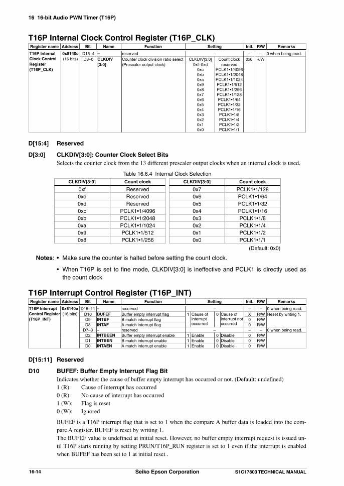
16 16-bit Audio PWM Timer (T16P)
16-14 Seiko Epson Corporation S1C17803 TECHNICAL MANUAL
T16P Internal Clock Control Register (T16P_CLK)Register name Address Bit Name Function Setting Init. R/W Remarks
T16P Internal Clock Control Register(T16P_CLK)
0x8140c(16 bits)
D15–4 – reserved – – – 0 when being read.D3–0 CLKDIV
[3:0]Counter clock division ratio select(Prescaler output clock)
CLKDIV[3:0] Count clock 0x0 R/W0xf–0xd
0xc0xb0xa0x90x80x70x60x50x40x30x20x10x0
reservedPCLK1•1/4096PCLK1•1/2048PCLK1•1/1024PCLK1•1/512PCLK1•1/256PCLK1•1/128PCLK1•1/64PCLK1•1/32PCLK1•1/16PCLK1•1/8PCLK1•1/4PCLK1•1/2PCLK1•1/1
D[15:4] Reserved
D[3:0] CLKDIV[3:0]: Counter Clock Select Bits Selects the counter clock from the 13 different prescaler output clocks when an internal clock is used.
Table 16.6.4 Internal Clock SelectionCLKDIV[3:0] Count clock CLKDIV[3:0] Count clock
0xf Reserved 0x7 PCLK1•1/1280xe Reserved 0x6 PCLK1•1/640xd Reserved 0x5 PCLK1•1/320xc PCLK1•1/4096 0x4 PCLK1•1/160xb PCLK1•1/2048 0x3 PCLK1•1/80xa PCLK1•1/1024 0x2 PCLK1•1/40x9 PCLK1•1/512 0x1 PCLK1•1/20x8 PCLK1•1/256 0x0 PCLK1•1/1
(Default: 0x0)
Notes: • Make sure the counter is halted before setting the count clock.
• When T16P is set to fine mode, CLKDIV[3:0] is ineffective and PCLK1 is directly used as the count clock
T16P Interrupt Control Register (T16P_INT)Register name Address Bit Name Function Setting Init. R/W Remarks
T16P Interrupt Control Register(T16P_INT)
0x8140e(16 bits)
D15–11 – reserved – – – 0 when being read.D10 BUFEF Buffer empty interrupt flag 1 Cause of
interrupt occurred
0 Cause of interrupt not occurred
X R/W Reset by writing 1.D9 INTBF B match interrupt flag 0 R/WD8 INTAF A match interrupt flag 0 R/W
D7–3 – reserved – – – 0 when being read.D2 INTBEEN Buffer empty interrupt enable 1 Enable 0 Disable 0 R/WD1 INTBEN B match interrupt enable 1 Enable 0 Disable 0 R/WD0 INTAEN A match interrupt enable 1 Enable 0 Disable 0 R/W
D[15:11] Reserved
D10 BUFEF: Buffer Empty Interrupt Flag Bit Indicates whether the cause of buffer empty interrupt has occurred or not. (Default: undefined) 1 (R): Cause of interrupt has occurred 0 (R): No cause of interrupt has occurred 1 (W): Flag is reset 0 (W): Ignored
BUFEF is a T16P interrupt flag that is set to 1 when the compare A buffer data is loaded into the com-pare A register. BUFEF is reset by writing 1.
The BUFEF value is undefined at initial reset. However, no buffer empty interrupt request is issued un-til T16P starts running by setting PRUN/T16P_RUN register is set to 1 even if the interrupt is enabled when BUFEF has been set to 1 at initial reset .

16 16-bit Audio PWM Timer (T16P)
S1C17803 TECHNICAL MANUAL Seiko Epson Corporation 16-15
D9 INTBF: B match Interrupt Flag Bit Indicates whether the cause of B match interrupt has occurred or not. 1 (R): Cause of interrupt has occurred 0 (R): No cause of interrupt has occurred (default) 1 (W): Flag is reset 0 (W): Ignored
INTBF is a T16P interrupt flag that is set to 1 when the counter reaches the value set in the compare B register. INTBF is reset by writing 1.
D8 INTAF: A match Interrupt Flag Bit Indicates whether the cause of A match interrupt has occurred or not. 1 (R): Cause of interrupt has occurred 0 (R): No cause of interrupt has occurred (default) 1 (W): Flag is reset 0 (W): Ignored
INTAF is a T16P interrupt flag that is set to 1 when the counter reaches the value set in the compare A register. INTAF is reset by writing 1.
D[7:3] Reserved
D2 INTBEEN: Buffer Empty Interrupt Enable Bit Enables or disables buffer empty interrupts. 1 (R/W): Interrupt enabled 0 (R/W): Interrupt disabled (default)
Setting INTBEEN to 1 enables buffer empty interrupt requests to the ITC. Setting it to 0 disables inter-rupts.
D1 INTBEN: B Match Interrupt Enable Bit Enables or disables B match interrupts. 1 (R/W): Interrupt enabled 0 (R/W): Interrupt disabled (default)
Setting INTBEN to 1 enables B match interrupt requests to the ITC. Setting it to 0 disables interrupts.
D0 INTAEN: A Match Interrupt Enable Bit Enables or disables A match interrupts. 1 (R/W): Interrupt enabled 0 (R/W): Interrupt disabled (default)
Setting INTAEN to 1 enables A match interrupt requests to the ITC. Setting it to 0 disables interrupts.

17 Watchdog Timer (WDT)
S1C17803 TECHNICAL MANUAL Seiko Epson Corporation 17-1
17 Watchdog Timer (WDT)
17.1 WDT Module OverviewThe S1C17803 incorporates a watchdog timer to detect the CPU running uncontrollably. The features of WDT are listed below.
• 30-bit up counter with a comparator
• Reset or NMI can be generated when the counter reaches the specified value if WDT has not been reset.
• The count clock is selectable from the system clock (PCLK2) and an external clock (EXCL0).
• Can output the generated NMI signal (#WDT_NMI) and the comparator output (WDT_CLK).
Figure 17.1.1 shows the WDT configuration.
RESEN
CLKSELRESET
Watchdog timer reset (WDRESEN)Watchdog timer Run/Stop control (RUNSTP)
Watchdog timer
NMIEN
CLKEN
NMI 30-bit comparison data register (CMPDT) Inte
rnal
dat
a bu
s
30-bit up counter (CTRDT)
CMUComparator
PCLK2
WDT_CLK
#WDT_NMI
Comparisonsignal
Clock output circuit
External clockEXCL0
Figure 17.1.1 WDT Configuration
The watchdog timer consists of a 30-bit up counter and comparison data register for generating an NMI or internal reset signal at programmable cycles. By resetting the watchdog timer within such a cycle in software so as not to generate NMI or internal reset signals, it is possible to detect a program running uncontrollably that does not ex-ecute that processing routine. The PCLK2 clock (= system clock) or external clock input for the 16-bit audio PWM timer (EXCL0) can be selected as the count clock for the watchdog timer. Moreover, a clock can be generated syn-chronously with NMI/reset generation cycles (set by the comparison data register) and output from the watchdog timer to external devices.
17.2 WDT Input/Output PinsTable 17.2.1 lists the input/output pins for the WDT module.
Table 17.2.1 List of WDT PinsPin name I/O Qty Function
EXCL0 I 1 T16P/WDT external clock input pinInputs an external clock as the counter clock.
WDT_CLK O 1 Watchdog timer clock output pinOutputs the reset/NMI cycle clock generated in the watchdog timer to external devices.
#WDT_NMI O 1 Watchdog timer NMI output pinOutputs the NMI signal generated in the watchdog timer to external devices.
The WDT input/output pins (EXCL0, WDT_CLK, #WDT_NMI) are shared with I/O ports and are initially set as general purpose I/O port pins. The pin functions must be switched using the port function select bits to use the gen-eral purpose I/O port pins as WDT input/output pins. For detailed information on pin function switching, see the “I/O Ports (GPIO)” chapter.

17 Watchdog Timer (WDT)
17-2 Seiko Epson Corporation S1C17803 TECHNICAL MANUAL
17.3 WDT Operating Clock The watchdog timer module is clocked by the PCLK2 clock (= system clock) supplied from the CMU. At initial reset, this clock is also selected as the count clock for the watchdog timer. For more information on clock generation and control, see the “Clock Management Unit (CMU)” chapter.
Note: Even when using an external clock as the count clock for the watchdog timer, PCLK2 is required for watchdog timer operation and access to its control register.
17.4 Control of the Watchdog Timer
17.4.1 Setting Up the Watchdog Timer
Selecting the count clock The internal clock (PCLK2) or an external clock (EXCL0) can be selected as the count clock for the 30-bit up-
counter by using CLKSEL/WD_EN register. Setting CLKSEL to 0 (default) selects the internal clock (PCLK2); setting it to 1 selects an external clock (EX-
CL0).
Setting the NMI/reset generation cycle The watchdog timer has a 30-bit comparison data register (CMPDT[29:0]/WD_CMP_L/H registers) that can be
used to set a cycle in which to generate an NMI or reset signal. The data set to CMPDT[29:0] is compared with the up-counter value. When both match, a specified NMI or
reset signal is output. The up-counter is reset to 0 at this time. The NMI/reset generation cycle can be calculated from the equation below.
CMPDT + 1NMI generating cycle = ———— [sec] fWDTIN
where CMPDT = value set to CMPDT[29:0] fWDTIN = Input clock (PCLK2 or EXCL0) frequency [Hz]
Note: Do not set a value equal to or less than 0x1f in the comparison data register.
Selecting the NMI/reset generation function To output an NMI signal when the watchdog timer is not reset within a specified cycle, set NMIEN/WD_EN
register to 1. To output a reset signal instead, set RESEN/WD_EN register to 1. Setting both bits to 0 (default) generates neither an NMI signal nor a reset signal, although the up-counter re-
mains active and can output a clock. Setting both bits to 1 outputs both an NMI signal and a reset signal. In this case, however, reset handling is ex-
ecuted since it has priority over the NMI handling. The NMI and reset signals are both output as pulses of 32 system clocks in width.
Note: Depending on the counter and comparison register values, an NMI or reset signal may be gener-ated after the NMI or reset function is enabled here (or even when the watchdog timer has not yet been started). Always be sure to set comparison data and reset the watchdog timer before writing 1 to NMIEN or RESEN.
Write protection of watchdog timer registers The WD_EN, WD_CMP_L, and WD_CMP_H registers are write-protected to prevent NMI or reset signals
from being inadvertently generated by unnecessary write operations. To rewrite these registers, write protection must be removed by writing 0x96 to WDPTC[15:0]/WD_WP register in 16-bit access only. Once the registers are rewritten, be sure to write other than 0x96 to WDPTC[15:0] to reapply write protection.

17 Watchdog Timer (WDT)
S1C17803 TECHNICAL MANUAL Seiko Epson Corporation 17-3
17.4.2 Starting/Stopping the Watchdog Timer
Writing 1 to RUNSTP/WD_EN register starts counting by the watchdog timer; writing 0 stops the watchdog timer. Since RUNSTP exists in the write-protected WD_EN register, write protection must be removed by writing 0x96 to WDPTC[15:0]/WD_WP register before the content of RUNSTP can be altered.
17.4.3 Resetting the Watchdog Timer
Before the NMI/reset generation function of the watchdog timer can be used, a routine to reset the watchdog timer before NMI or reset generation must be prepared in a location for periodic processing. Make sure that this routine is processed within the NMI/reset generation cycle described earlier.Writing 1 to WDRESEN/WD_CTL register resets the watchdog timer. The up-counter is reset to 0 at this time, then starts counting NMI/reset generation cycles all over again.If the watchdog timer is not reset within the set cycle for some reason, the CPU is placed into trap handling by an NMI or reset signal to execute the processing routine. The reset and NMI vector addresses are set by default to 0x8000 and 0x8008, respectively. The vector table base address can be altered by using TTBR. The count value of the up-counter can be read out from CTRDT[29:0]/WD_CNT_L/H registers at any time.
17.4.4 Operation in Standby Mode
In HALT mode In HALT mode, the watchdog timer remains active as it is supplied with a clock. Therefore, if HALT mode re-
mains active beyond the NMI/reset generation cycle, an NMI or reset signal deactivates HALT mode. To disable the watchdog timer in HALT mode, set NMIEN/WD_EN register or RESEN/WD_EN register to 0.
Otherwise, write 0 to RUNSTP/WD_EN register to stop the watchdog timer before executing the halt instruc-tion.
When NMIEN or RESEN disables NMI or reset generation, the watchdog timer continues counting even in HALT mode. To reenable NMI or reset generation after exiting HALT mode, be sure to reset the watchdog timer beforehand.
When HALT mode is entered after stopping the watchdog timer, be sure to reset the watchdog timer before re-starting it.
In SLEEP mode The supply of PCLK2 from the CMU stops in SLEEP mode. Therefore, the watchdog timer also stops operat-
ing. To prevent an unnecessary NMI or reset signal from being generated after exiting SLEEP mode, be sure to reset the watchdog timer before executing the slp instruction. Moreover, disable NMI/reset generation by set-ting NMIEN or RESEN as required.
17.4.5 Clock Output of the Watchdog Timer
The watchdog timer can output an NMI/reset generation cycle-synchronous clock from the IC to external devices. For this clock output, set CLKEN/WD_EN register to 1 after setting up the WDT_CLK pin.Since CLKEN also exists in the write-protected WDT_EN register, write protection must be removed by writing 0x96 to WDPTC[15:0]/WD_WP register before the content of CLKEN can be altered.
If the watchdog timer is not reset in software, the level of clock output from the IC is reversed synchronously with the NMI generation cycles. (This applies when reset generation is disabled.)When the watchdog timer is reset in software, clock output from the IC goes low at that time and remains low.

17 Watchdog Timer (WDT)
17-4 Seiko Epson Corporation S1C17803 TECHNICAL MANUAL
Input clock
Counter data
Comparison data
Comparison match signal
WDT_CLK output clock
FFFF1D FFFF1E FFFF1F FFFF20
FFFF20
0 1 2 FFFF1F FFFF20 0 1 2
Figure 17.4.5.1 Clock Output of Watchdog Timer
17.4.6 External NMI Output
The watchdog timer can output the NMI signal generated to external devices. The watchdog timer uses the #WDT_NMI pin for this output. Setting NMIEN/WD_EN register to 1 enables the external NMI signal output as well as the internal NMI signal output. When the watchdog timer counter reaches the comparison data, the #WDT_NMI pin outputs a low pulse with 32 system clock cycles.
Input clock
Counter data
Comparison data
#WDT_NMI output
FFFF1D FFFF1E FFFF1F FFFF20
FFFF20
32 system clock cycles
0 1 2 1E 1F 20 21 22
Figure 17.4.6.1 External NMI Output
17.5 Control Register Details
Table 17.5.1 List of WDT RegistersAddress Register name Function
0x81060 WD_WP WDT Write Protect Register Enables WDT control registers for writing.0x81062 WD_EN WDT Enable and Setup Register Configures and starts watchdog timer.0x81064 WD_CMP_L WDT Comparison Data L Register Comparison data
0x81066 WD_CMP_H WDT Comparison Data H Register0x81068 WD_CNT_L WDT Count Data L Register Watchdog timer counter data0x8106a WD_CNT_H WDT Count Data H Register0x8106c WD_CTL WDT Control Register Resets watchdog timer.
The following describes each WDT register. These are all 16-bit registers.
Notes: • When data is written to the registers, the “Reserved” bits must always be written as 0 and not 1.
• The WD_WP register (0x81060) allows 16-bit access only. Other registers (0x81062 to 0x8106c) allow 8-bit access as well as 16-bit access.
WDT Write Protect Register (WD_WP)Register name Address Bit Name Function Setting Init. R/W Remarks
WDT Write Protect Register(WD_WP)
0x81060(16 bits)
D15–0 WDPTC[15:0]
WDT register write protect flag Writing 0x96 removes the write protection of the WD_EN, WD_CMP_L, and WD_CMP_H registers.Writing another value set the write protection.
X W 0 when being read.
D[15:0] WDPTC[15:0]: WDT Register Write Protect Flag Bits These bits set or clear write protection at addresses 0x81062 to 0x81066. 0x96 (W): Clears write protection Other than 0x96 (W): Applies write protection (default, indeterminate value) 0x0 (R): Always 0x0 when read

17 Watchdog Timer (WDT)
S1C17803 TECHNICAL MANUAL Seiko Epson Corporation 17-5
Before altering the WDT_EN, WDT_CMP_L, or WDT_CMP_H register, write 0x96 to WDPTC[15:0] to remove write protection. Setting WDPTC[15:0] to other than 0x96 will result in the contents of the registers above not being altered even when executing the write instruction without any problem. Once write protection is removed by writing 0x96 to WDPTC[15:0], said registers can be rewritten any number of times until WDPTC[15:0] is set to other than 0x96. When the WDT_EN, WDT_CMP_L, or WDT_CMP_H have been rewritten, be sure to write other than 0x96 to WDPTC[15:0] to prevent erro-neous writing to the registers.
WDT Enable and Setup Register (WD_EN)Register name Address Bit Name Function Setting Init. R/W Remarks
WDT Enable and Setup Register(WD_EN)
0x81062(16 bits)
D15–7 – reserved – – – 0 when being read.D6 CLKSEL WDT input clock select 1 External clk 0 Internal clk 0 R/W Write-protectedD5 CLKEN WDT clock output control 1 On 0 Off 0 R/WD4 RUNSTP WDT Run/Stop control 1 Run 0 Stop 0 R/W
D3–2 – reserved – – – 0 when being read.D1 NMIEN WDT NMI enable 1 Enable 0 Disable 0 R/W Write-protectedD0 RESEN WDT RESET enable 1 Enable 0 Disable 0 R/W
Note: This register is write-protected to prevent NMI or reset signals from being inadvertently generated by unnecessary write operations. To rewrite this register, write protection must be removed by writing 0x96 to WDPTC[15:0]/WD_WP register. Once the register has been rewritten, be sure to write other than 0x96 to WDPTC[15:0] to reapply write protection.
D[15:7] Reserved
D6 CLKSEL: WDT Input Clock Select Bit This bit selects the count clock for the watchdog timer. 1 (R/W): External clock (EXCL0) 0 (R/W): Internal clock (PCLK2) (default)
Setting this bit to 0 (default) selects the internal clock (PCLK2); setting it to 1 selects the external clock (EXCL0).
D5 CLKEN: WDT Clock Output Control Bit This bit controls the clock output of the watchdog timer. 1 (R/W): On 0 (R/W): Off (default)
Setting this bit to 1 outputs an NMI/reset generation cycle-synchronous clock from the IC.
D4 RUNSTP: WDT Run/Stop Control Bit This bit starts or stops the watchdog timer. 1 (R/W): Start 0 (R/W): Stop (default)
When the NMI or reset generation function is enabled, be sure to set comparison data and reset the watchdog timer before starting the watchdog timer, thus preventing the generation of unnecessary NMI or reset signals.
D[3:2] Reserved
D1 NMIEN: WDT NMI Enable Bit This bit enables NMI signal output by the watchdog timer. 1 (R/W): Enable 0 (R/W): Disable (default)
Setting this bit to 1 outputs an NMI signal (a pulse 32 system clocks in width) to the CMU and the #WDT_NMI pin when the count of the up-counter matches the value set in the comparison data regis-ter. Setting this bit to 0 outputs no NMI signals.
Regardless of how this bit is set, the up-counter is reset to 0 when the up-counter and set value of the comparison data register match, then starts counting all over again.

17 Watchdog Timer (WDT)
17-6 Seiko Epson Corporation S1C17803 TECHNICAL MANUAL
D0 RESEN: WDT RESET Enable Bit This bit enables internal reset signal output by the watchdog timer. 1 (R/W): Enable 0 (R/W): Disable (default)
Setting this bit to 1 outputs a reset signal (a pulse 32 system clocks in width) to the CMU when the count of the up-counter matches the value set in the comparison data register. Setting this bit to 0 out-puts no reset signals.
WDT Comparison Data L/H Registers (WD_CMP_L, WD_CMP_H)Register name Address Bit Name Function Setting Init. R/W Remarks
WDT Com-parison Data L Register (WD_CMP_L)
0x81064(16 bits)
D15–0 CMPDT[15:0]
WDT comparison dataCMPDT0 = LSB
0x0 to 0x3fffffff(low-order 16 bits)
0x0 R/W Write-protected
WDT Com-parison Data H Register (WD_CMP_H)
0x81066(16 bits)
D15–14 – reserved – – – 0 when being read.D13-0 CMPDT
[29:16]WDT comparison dataCMPDT29 = MSB
0x0 to 0x3fffffff(high-order 14 bits)
0x0 R/W Write-protected
Note: These registers are write-protected to prevent NMI or reset signals from being inadvertently gen-erated by unnecessary write operations. To rewrite these registers, write protection must be re-moved by writing 0x96 to WDPTC[15:0]/WD_WP register. Once the registers have been rewritten, be sure to write other than 0x96 to WDPTC[15:0] to reapply write protection.
D[13:0]/0x81066, D[15:0]/0x81064 CMPDT[29:0]: WDT Comparison Data Bits Sets comparison data. (Default: 0x0) Use these registers to set the NMI/reset generation cycle. With NMI or reset generation enabled, an NMI or reset signal is output when the up-counter matches
the comparison data set in these registers. When a clock is output from the watchdog timer, these registers also set the output clock cycle.
Note: Do not set a value equal to or less than 0x1f as comparison data.
WDT Count Data L/H Registers (WD_CNT_L, WD_CNT_H)Register name Address Bit Name Function Setting Init. R/W Remarks
WDT Count Data L Register (WD_CNT_L)
0x81068(16 bits)
D15–0 CTRDT[15:0]
WDT counter dataCTRDT0 = LSB
0x0 to 0x3fffffff(low-order 16 bits)
X R
WDT Count Data H Register (WD_CNT_H)
0x8106a(16 bits)
D15–14 – reserved – – – 0 when being read.D13-0 CTRDT
[29:16]WDT counter dataCTRDT29 = MSB
0x0 to 0x3fffffff(high-order 14 bits)
X R
D[13:0]/0x8106a, D[15:0]/0x81068 CTRDT[29:0]: WDT Counter Data Bits The current count value of the 30-bit up-counter can be read out from these registers. (Default: indeterminate)
WDT Control Register (WD_CTL)Register name Address Bit Name Function Setting Init. R/W Remarks
WDT Control Register(WD_CTL)
0x8106c(16 bits)
D15–1 – reserved – – – 0 when being read.
D0 WDRESEN WDT reset 1 Reset 0 ignored 0 W
D[15:1] Reserved
17 Watchdog Timer (WDT)
S1C17803 TECHNICAL MANUAL Seiko Epson Corporation 17-7
D0 WDRESEN: WDT Reset Bit This bit resets the watchdog timer. 1 (W): Reset 0 (W): Has no effect 0 (R): Always 0 when read (default)
With NMI or reset signal output enabled, the watchdog timer must be reset by writing 1 to this bit with-in the set NMI/reset generation cycle. The up-counter is thereby reset to 0, then starts counting NMI/reset generation cycles all over again.

18 UART
S1C17803 TECHNICAL MANUAL Seiko Epson Corporation 18-1
18 UART
18.1 UART Module OverviewThe S1C17803 incorporates a UART module. The UART transfers asynchronous data with external serial devices.The following shows the main features of the UART:
• Transfer rate: 150 to 460,800 bps (150 to 115,200 bps in IrDA mode)
• Transfer clock: Internal clock (CLG_T16FU0 output) or an external clock input (SCLK input) can be selected.
• Character length: 7 or 8 bits (LSB first)
• Parity mode: Even, odd, or no parity
• Stop bit: 1 or 2 bits
• Start bit: 1 bit fixed
• Includes a 2-byte receive data buffer and a 1-byte transmit data buffer.
• Includes an RZI modulator/demodulator circuit to support IrDA 1.0-compatible infrared communications.
• Can detect parity error, framing error, and overrun error during receiving.
• Can generate receive buffer full, transmit buffer empty and receive error interrupts.
Figure 18.1.1 shows the UART configuration.
Shift registerReceive data
buffer (2 bytes)SIN
sclk (from CLG_T16FU0)
Internal bus
ITC
UART
Bus I/Fand
controlregisters
#SCLK
Shift registerTransmit data buffer (1 byte)
Clock/transfer control
SOUT
RZIdemodulator
RZImodulator
Interruptcontrol
Figure 18.1.1 UART Configuration
18.2 UART Input/Output PinsTable 18.2.1 lists the UART input/output pins.
Table 18.2.1 List of UART PinsPin name I/O Qty Function
SIN I 1 UART data input pinInputs serial data sent from an external serial device.
SOUT O 1 UART data output pinOutputs serial data sent to an external serial device.
#SCLK I 1 UART clock input pinInputs the transfer clock when an external clock is used.
The UART input/output pins (SIN, SOUT, SCLK) are shared with I/O ports and are initially set as general purpose I/O port pins. The pin functions must be switched using the port function select bits to use the general purpose I/O port pins as UART input/output pins.For detailed information on pin function switching, see the “I/O Ports (GPIO)” chapter.

18 UART
18-2 Seiko Epson Corporation S1C17803 TECHNICAL MANUAL
18.3 Transfer ClockThe UART transfer clock can be set to internal or external using SSCK/UART_MOD register.
Note: Make sure the UART is halted (RXEN/UART_CTL register = 0) before changing SSCK.
Internal clock Setting SSCK to 0 (default) selects the internal clock. The UART uses the CLG_T16FU0 output clock. Thus,
CLG_T16FU0 must be programmed to output a clock suited to the transfer rate. For more information on con-trolling CLG_T16FU0, see the “Clock Generator (CLG)” chapter.
External clock Setting SSCK to 1 selects an external clock. In this case, input the external clock to the #SCLK pin.
Notes: • The UART generates a sampling clock by dividing the CLG_T16FU0 output clock or external clock by 16. Be careful when setting the transfer rate.
• When inputting an external clock via the #SCLK pin, the clock frequency must be half of the system clock or less and has a duty ratio of 50%.
18.4 Transfer Data SettingsSet the following conditions to configure the transfer data format.• Data length: 7 or 8 bits• Start bit: Fixed at 1 bit• Stop bit: 1 or 2 bits• Parity bit: Even, odd, or no parity
Note: Make sure the UART is halted (RXEN/UART_CTL register = 0) before changing transfer data for-mat settings.
Data length The data length is selected by CHLN/UART_MOD register. Setting CHLN to 0 (default) configures the data
length to 7 bits. Setting CHLN to 1 configures it to 8 bits.
Stop bit The stop bit length is selected by STPB/UART_MOD register. Setting STPB to 0 (default) configures the stop
bit length to 1 bit. Setting STPB to 1 configures it to 2 bits.
Parity bit Whether the parity function is enabled or disabled is selected by PREN/UART_MOD register. Setting PREN
to 0 (default) disables the parity function. In this case, no parity bit is added to the transfer data and the data is not checked for parity when received. Setting PREN to 1 enables the parity function. In this case, a parity bit is added to the transfer data and the data is checked for parity when received.
When the parity function is enabled, the parity mode is selected by PMD/UART_MOD register. Setting PMD to 0 (default) adds a parity bit and checks for even parity. Setting PMD to 1 adds a parity bit and checks for odd parity.

18 UART
S1C17803 TECHNICAL MANUAL Seiko Epson Corporation 18-3
Sampling clock (sclk•1/16)
CHLN = 0, PREN = 0, STPB = 0
CHLN = 0, PREN = 1, STPB = 0
CHLN = 0, PREN = 0, STPB = 1
CHLN = 0, PREN = 1, STPB = 1
CHLN = 1, PREN = 0, STPB = 0
CHLN = 1, PREN = 1, STPB = 0
CHLN = 1, PREN = 0, STPB = 1
CHLN = 1, PREN = 1, STPB = 1
s1 D0 D1 D2 D3 D4 D5 D6 s2
s1 D0 D1 D2 D3 D4 D5 D6 p s2
s1 D0 D1 D2 D3 D4 D5 D6 s2 s3
s1 D0 D1 D2 D3 D4 D5 D6 p s2 s3
s1 D0 D1 D2 D3 D4 D5 D6 D7 s2
s1 D0 D1 D2 D3 D4 D5 D6 D7 p s2
s1 D0 D1 D2 D3 D4 D5 D6 D7 s2 s3
s1 D0 D1 D2 D3 D4 D5 D6 D7 p s2 s3
s1: start bit, s2 & s3: stop bit, p: parity bit
Figure 18.4.1 Transfer Data Format
18.5 Data Transfer ControlMake the following settings before starting data transfers.(1) Select the input clock. (See Section 18.3.) To use the internal clock, program CLG_T16FU0 to output the transfer clock. See the CLG chapter.(2) Set the transfer data format. (See Section 18.4.)(3) To use the IrDA interface, set IrDA mode. (See Section 18.8.)(4) Set interrupt conditions to use UART interrupts. (See Section 18.7.)
Note: Make sure the UART is halted (RXEN/UART_CTL register = 0) before changing the above set-tings.
Enabling data transfers Set RXEN/UART_CTL register to 1 to enable data transfers. This puts the transmitter/receiver circuit in ready-
to-transmit/receive status.
Note: Do not set RXEN to 0 while the UART is sending or receiving data.
Data transmission control To start data transmission, write the transmit data to TXD[7:0]/UART_TXD register. The data is written to the transmit data buffer, and the transmitter circuit starts sending data. The buffer data is sent to the transmit shift register, and the start bit is output from the SOUT pin. The data in
the shift register is then output from the LSB. The transfer data bit is shifted in sync with the sampling clock rising edge and output in sequence via the SOUT pin. Following output of MSB, the parity bit (if parity is en-abled) and the stop bit are output.
The transmitter circuit includes two status flags: TDBE/UART_ST register and TRBS/UART_ST register. The TDBE flag indicates the transmit data buffer status. This flag switches to 0 when the application program
writes data to the transmit data buffer and reverts to 1 when the buffer data is sent to the transmit shift register. An interrupt can be generated when this flag is set to 1 (see Section 18.7). Subsequent data is sent after con-firming that the transmit data buffer is empty either by using this interrupt or by reading the TDBE flag. The transmit data buffer size is 1 byte, but a shift register is provided separately to allow data to be written while the previous data is being sent. Always confirm that the transmit data buffer is empty before writing transmit data. Writing data while the TDBE flag is 0 will overwrite earlier transmit data inside the transmit data buffer.
The TRBS flag indicates the shift register status. This flag switches to 1 when transmit data is loaded from the transmit data buffer to the shift register and reverts to 0 once the data is sent. Read this flag to check whether the transmitter circuit is operating or at standby.

18 UART
18-4 Seiko Epson Corporation S1C17803 TECHNICAL MANUAL
S1: Start bit, S2: Stop bit, P: Parity bit, Wr: Data write to transmit data buffer
Sampling clock
SOUT
TDBE
TRBS
Interrupt
S1 D0 D1 D2 D3 D4 D5 D6 D7 P S2 S1 D0 D1 D7 P S2 S1 D0 D1 D7 P
Wr Wr Wr
S2
Transmit buffer empty interrupt request
Figure 18.5.1 Data Transmission Timing Chart
Data reception control The receiver circuit is activated by setting RXEN to 1, enabling data to be received from an external serial de-
vice. When the external serial device sends a start bit, the receiver circuit detects its Low level and starts sampling
the following data bits. The data bits are sampled at the sampling clock rising edge, and the lead bit is loaded into the receive shift register as LSB. Once the MSB has been received into the shift register, the received data is loaded into the receive data buffer. If parity checking is enabled, the receiver circuit checks the received data at the same time by checking the parity bit received immediately after the MSB.
The receive data buffer, a 2-byte FIFO, receives data until full.
Received data in the buffer can be read from RXD[7:0]/UART_RXD register. The oldest data is read out first and data is cleared by reading.
The receiver circuit includes two buffer status flags: RDRY/UART_ST register and RD2B/UART_ST register. The RDRY flag indicates that the receive data buffer still contains data. The RD2B flag indicates that the re-
ceive data buffer is full.
(1) RDRY = 0, RD2B = 0 The receive data buffer contents need not be read, since no data has been received.
(2) RDRY = 1, RD2B = 0 One 8-bit data has been received. Read the receive data buffer contents once. This resets the RDRY flag.
The buffer reverts to state (1) above. If the receive data buffer contents are read twice, the second data read will be invalid.
(3) RDRY = 1, RD2B = 1 Two 8-bit data have been received. Read the receive data buffer contents twice. The receive data buffer
outputs the oldest data first, resetting the RD2B flag. The buffer then reverts to the state in (2) above. The second read outputs the most recent received data, after which the buffer reverts to the state in (1) above.
Even when the receive data buffer is full, the shift register can start to receive one more 8-bit data. If the receive data buffer is not read out by the time the third data has been fully received, an overrun error will occur and the third data in the shift register will be disposed. The contents of the receive data buffer must be read out before an overrun error occurs. For detailed information on overrun errors, refer to Section 18.6.
The volume of data received can be checked by reading these flags. The UART allows receive buffer full interrupts to be generated once data has been received in the receive data
buffer. These interrupts can be used to read the receive data buffer. By default, a receive buffer full interrupt occurs when the receive data buffer receives one 8-bit data (status (2) above). This can be changed by setting RBFI/UART_CTL register to 1 so that an interrupt occurs when the receive data buffer receives two 8-bit data.
Three error flags are also provided in addition to the flags previously mentioned. See Section 18.6 for detailed information on flags and receive errors.

18 UART
S1C17803 TECHNICAL MANUAL Seiko Epson Corporation 18-5
Receive buffer full interrupt request(RBFI = 0)
Overrun error interrupt request
Sampling clock
SIN
Receive data buffer
RDRY
RD2B
RXD[7:0]
Interrupt
data 1S1 D0 ··· P S2 S1 D0 ··· P S2 S1 D0 ··· P S2 S1 D0 ··· P S2 S1 D0 ··· P S2 S1 D0 ··· P S2
data 2 data 3 data 4 data 5 data 6
Rd
Rd
data 3, 4data 2data 1 – data 2, 3 data 3
data 3data 2data 1
S1: Start bit, S2: Stop bit, P: Parity bit, Rd: Data read from RXD[7:0]
Figure 18.5.2 Data Receiving Timing Chart
Disabling data transfers After a data transfer is completed (both transmission and reception), write 0 to RXEN to disable data transfers.
Make sure that the TDBE flag is 1 and the TRBS and RDRY flags are both 0 before disabling data transfer. Setting RXEN to 0 empties the transmit and receive data buffers, clearing any remaining data. The data being
transferred cannot be guaranteed if RXEN is set to 0 while data is being sent or received.
18.6 Receive ErrorsThree different receive errors may be detected while receiving data.Since receive errors are interrupt causes, they can be processed by generating interrupts. For more information on UART interrupt control, see Section 18.7.
Parity error If PREN/UART_MOD register has been set to 1 (parity enabled), data received is checked for parity. Data received in the shift register is checked for parity when sent to the receive data buffer. The matching is
checked against the PMD/UART_MOD register setting (odd or even parity). If the result is a non-match, a par-ity error is issued, and the parity error flag PER/UART_ST register is set to 1. Even if this error occurs, the data received is sent to the receive data buffer, and the receiving operation continues. However, the received data cannot be guaranteed if a parity error occurs. The PER flag is reset to 0 by writing 1.
Framing error A framing error occurs if the stop bit is received as 0 and the UART determines loss of sync. If the stop bit is
set to two bits, only the first bit is checked. The framing error flag FER/UART_ST register is set to 1 if this error occurs. The received data is still trans-
ferred to the receive data buffer if this error occurs and the receiving operation continues, but the data cannot be guaranteed, even if no framing error occurs for subsequent data receiving. The FER flag is reset to 0 by writing 1.
Overrun error Even if the receive data buffer is full (two 8-bit data already received), the third data can be received in the shift
register. However, if the receive data buffer is not emptied (by reading out data received) by the time this data has been received, the third data received in the shift register will not be sent to the buffer, and an overrun error will take place. If an overrun error occurs, the overrun error flag OER/UART_ST register is set to 1. The receiv-ing operation continues even if this error occurs. The OER flag is reset to 0 by writing 1.

18 UART
18-6 Seiko Epson Corporation S1C17803 TECHNICAL MANUAL
18.7 UART InterruptsThe UART includes a function for generating the following three different types of interrupts.• Transmit buffer empty interrupt• Receive buffer full interrupt• Receive error interrupt
The UART outputs one interrupt signal shared by the three above interrupt causes to the interrupt controller (ITC). Inspect the status flag and error flag to determine the interrupt cause occurred.
Transmit buffer empty interrupt To use this interrupt, set TIEN/UART_CTL register to 1. If TIEN is set to 0 (default), interrupt requests for this
cause will not be sent to the ITC. When transmit data written to the transmit data buffer is transferred to the shift register, the UART sets TDBE/
UART_ST register to 1, indicating that the transmit data buffer is empty. If transmit buffer empty interrupts are enabled (TIEN = 1), an interrupt request is sent simultaneously to the ITC.
An interrupt occurs if other interrupt conditions are met. You can inspect the TDBE flag in the UART interrupt handler routine to determine whether the UART interrupt is attributable to a transmit buffer empty. If TDBE is 1, the next transmit data can be written to the transmit data buffer by the interrupt handler routine.
Receive buffer full interrupt To use this interrupt, set RIEN/UART_CTL register to 1. If RIEN is set to 0 (default), interrupt requests for this
cause will not be sent to the ITC. If the specified volume of received data is loaded into the receive data buffer when a receive buffer full inter-
rupt is enabled (RIEN = 1), the UART outputs an interrupt request to the ITC. If RBFI/UART_CTL register is 0, an interrupt request is output as soon as one received data is loaded into the receive data buffer (when RDRY/UART_ST register is set to 1). If RBFI is 1, an interrupt request is output as soon as two received data are load-ed into the receive data buffer (when RD2B/UART_ST register is set to 1).
An interrupt occurs if other interrupt conditions are met. You can inspect the RDRY and RD2B flags in the UART interrupt handler routine to determine whether the UART interrupt is attributable to a receive buffer full. If RDRY or RD2B is 1, the received data can be read from the receive data buffer by the interrupt handler rou-tine.
Receive error interrupt To use this interrupt, set REIEN/UART_CTL register to 1. If REIEN is set to 0 (default), interrupt requests for
this cause will not be sent to the ITC. The UART sets an error flag, PER, FER, or OER/UART_ST register to 1 if a parity error, framing error, or
overrun error is detected when receiving data. If receive error interrupts are enabled (REIEN = 1), an interrupt request is sent simultaneously to the ITC.
If other interrupt conditions are satisfied, an interrupt occurs. You can inspect the PER, FER, and OER flags in the UART interrupt handler routine to determine whether the UART interrupt was caused by a receive error. If any of the error flags has the value 1, the interrupt handler routine will proceed with error recovery.
For more information on interrupt processing, see the “Interrupt Controller (ITC)” chapter.
18.8 IrDA InterfaceThis UART module incorporates an RZI modulator/demodulator circuit enabling implementation of IrDA 1.0-compatible infrared communication function simply by adding basic external circuits.
The transmit data output from the UART transmit shift register is input to the modulator circuit and output from the SOUT pin after the Low pulse has been modulated to a 3/16 sclk cycle.

18 UART
S1C17803 TECHNICAL MANUAL Seiko Epson Corporation 18-7
sclk
Modulator input (shift register output)
Modulator output (SOUT)
1 2 3 8 9 10 11 16
3 × sclk
Modulator input (shift register output)
Modulator output (SOUT)
S1 D0 D1 D2 D3 D4 D5 D6 D7 P S2 S3
(S1: Start bit, S2 & S3: Stop bits, P: Parity bit)
Figure 18.8.1 Transmission Signal Waveform
The received IrDA signal is input to the demodulator circuit and the Low pulse width is converted to 16 sclk cycles before entry to the receive shift register. The demodulator circuit uses the pulse detection clock selected from the prescaler output clock separately from the transfer clock to detect Low pulses input (when minimum pulse width = 1.41 µs/115,200 bps).
(S1: Start bit, S2 & S3: Stop bits, P: Parity bit)
sclk
irclk
Demodulator input (SIN)
Demodulator output (shift register input)
1 2 3 4 16
16 × sclk2 × irclk or more
Demodulator input (SIN)
Demodulator output (shift register input) S1 D0 D1 D2 D3 D4 D5 D6 D7 P S2 S3
Figure 18.8.2 Receive Signal Waveform
IrDA enable To use the IrDA interface function, set IRMD/UART_EXP register to 1. This enables the RZI modulator/de-
modulator circuit.
Note: This setting must be performed before setting other UART conditions.
IrDA receive detection clock selection The input pulse detection clock is selected from among the prescaler output clock PCLK_SOC•1/1 to PCLK_
SOC•1/128 using IRCLK[2:0]/UART_EXP register.
Table 18.8.1 IrDA Receive Detection Clock SelectionIRCLK[2:0] Prescaler output clock
0x7 PCLK_SOC•1/1280x6 PCLK_SOC•1/640x5 PCLK_SOC•1/320x4 PCLK_SOC•1/160x3 PCLK_SOC•1/80x2 PCLK_SOC•1/40x1 PCLK_SOC•1/20x0 PCLK_SOC•1/1
(Default: 0x0)
This clock must be selected as a clock faster than the fine mode 16-bit timer or transfer clock sclk input via the #SCLK pin.
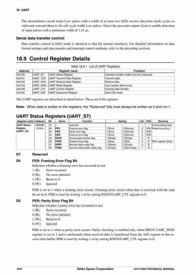
18 UART
18-8 Seiko Epson Corporation S1C17803 TECHNICAL MANUAL
The demodulator circuit treats Low pulses with a width of at least two IrDA receive detection clock cycles as valid and converts them to 16 sclk cycle width Low pulses. Select the prescaler output clock to enable detection of input pulses with a minimum width of 1.41 µs.
Serial data transfer control Data transfer control in IrDA mode is identical to that for normal interfaces. For detailed information on data
format settings and data transfer and interrupt control methods, refer to the preceding sections.
18.9 Control Register DetailsTable 18.9.1 List of UART Registers
Address Register name Function0x4100 UART_ST UART Status Register Indicates transfer, buffer and error statuses.0x4101 UART_TXD UART Transmit Data Register Transmit data0x4102 UART_RXD UART Receive Data Register Receive data
0x4103 UART_MOD UART Mode Register Sets transfer data format.0x4104 UART_CTL UART Control Register Controls data transfer.
0x4105 UART_EXP UART Expansion Register Sets IrDA mode.
The UART registers are described in detail below. These are 8-bit registers.
Note: When data is written to the registers, the “Reserved” bits must always be written as 0 and not 1.
UART Status Registers (UART_ST)Register name Address Bit Name Function Setting Init. R/W Remarks
UART Status Register(UART_ST)
0x4100(8 bits)
D7 – reserved – – – 0 when being read.D6 FER Framing error flag 1 Error 0 Normal 0 R/W Reset by writing 1.D5 PER Parity error flag 1 Error 0 Normal 0 R/WD4 OER Overrun error flag 1 Error 0 Normal 0 R/WD3 RD2B Second byte receive flag 1 Ready 0 Empty 0 RD2 TRBS Transmit busy flag 1 Busy 0 Idle 0 R Shift register statusD1 RDRY Receive data ready flag 1 Ready 0 Empty 0 RD0 TDBE Transmit data buffer empty flag 1 Empty 0 Not empty 1 R
D7 Reserved
D6 FER: Framing Error Flag Bit Indicates whether a framing error has occurred or not. 1 (R): Error occurred 0 (R): No error (default) 1 (W): Reset to 0 0 (W): Ignored
FER is set to 1 when a framing error occurs. Framing errors occur when data is received with the stop bit set to 0. FER is reset by writing 1 or by setting RXEN/UART_CTL register to 0.
D5 PER: Parity Error Flag Bit Indicates whether a parity error has occurred or not. 1 (R): Error occurred 0 (R): No error (default) 1 (W): Reset to 0 0 (W): Ignored
PER is set to 1 when a parity error occurs. Parity checking is enabled only when PREN/ UART_MOD register is set to 1 and is performed when received data is transferred from the shift register to the re-ceive data buffer. PER is reset by writing 1 or by setting RXEN/UART_CTL register to 0.
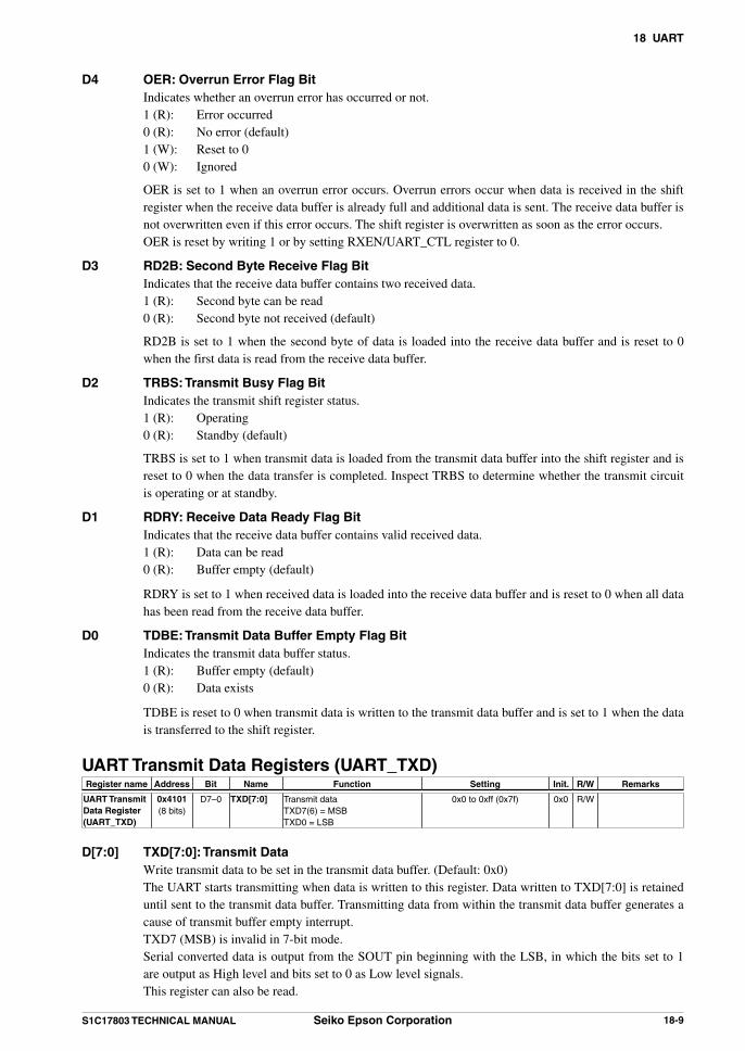
18 UART
S1C17803 TECHNICAL MANUAL Seiko Epson Corporation 18-9
D4 OER: Overrun Error Flag Bit Indicates whether an overrun error has occurred or not. 1 (R): Error occurred 0 (R): No error (default) 1 (W): Reset to 0 0 (W): Ignored
OER is set to 1 when an overrun error occurs. Overrun errors occur when data is received in the shift register when the receive data buffer is already full and additional data is sent. The receive data buffer is not overwritten even if this error occurs. The shift register is overwritten as soon as the error occurs.
OER is reset by writing 1 or by setting RXEN/UART_CTL register to 0.
D3 RD2B: Second Byte Receive Flag Bit Indicates that the receive data buffer contains two received data. 1 (R): Second byte can be read 0 (R): Second byte not received (default)
RD2B is set to 1 when the second byte of data is loaded into the receive data buffer and is reset to 0 when the first data is read from the receive data buffer.
D2 TRBS: Transmit Busy Flag Bit Indicates the transmit shift register status. 1 (R): Operating 0 (R): Standby (default)
TRBS is set to 1 when transmit data is loaded from the transmit data buffer into the shift register and is reset to 0 when the data transfer is completed. Inspect TRBS to determine whether the transmit circuit is operating or at standby.
D1 RDRY: Receive Data Ready Flag Bit Indicates that the receive data buffer contains valid received data. 1 (R): Data can be read 0 (R): Buffer empty (default)
RDRY is set to 1 when received data is loaded into the receive data buffer and is reset to 0 when all data has been read from the receive data buffer.
D0 TDBE: Transmit Data Buffer Empty Flag Bit Indicates the transmit data buffer status. 1 (R): Buffer empty (default) 0 (R): Data exists
TDBE is reset to 0 when transmit data is written to the transmit data buffer and is set to 1 when the data is transferred to the shift register.
UART Transmit Data Registers (UART_TXD)Register name Address Bit Name Function Setting Init. R/W Remarks
UART Transmit Data Register(UART_TXD)
0x4101(8 bits)
D7–0 TXD[7:0] Transmit dataTXD7(6) = MSBTXD0 = LSB
0x0 to 0xff (0x7f) 0x0 R/W
D[7:0] TXD[7:0]: Transmit Data Write transmit data to be set in the transmit data buffer. (Default: 0x0) The UART starts transmitting when data is written to this register. Data written to TXD[7:0] is retained
until sent to the transmit data buffer. Transmitting data from within the transmit data buffer generates a cause of transmit buffer empty interrupt.
TXD7 (MSB) is invalid in 7-bit mode. Serial converted data is output from the SOUT pin beginning with the LSB, in which the bits set to 1
are output as High level and bits set to 0 as Low level signals. This register can also be read.

18 UART
18-10 Seiko Epson Corporation S1C17803 TECHNICAL MANUAL
UART Receive Data Registers (UART_RXD)Register name Address Bit Name Function Setting Init. R/W Remarks
UART Receive Data Register(UART_RXD)
0x4102(8 bits)
D7–0 RXD[7:0] Receive data in the receive data bufferRXD7(6) = MSBRXD0 = LSB
0x0 to 0xff (0x7f) 0x0 R Older data in the buf-fer is read out first.
D[7:0] RXD[7:0]: Receive Data Data in the receive data buffer is read out in sequence, starting with the oldest. Received data is placed in
the receive data buffer. The receive data buffer is a 2-byte FIFO that allows proper data reception until it fills, even if data is not read out. If the buffer is full and the shift register also contains received data, an overrun error will occur, unless the data is read out before reception of the subsequent data starts.
The receive circuit includes two receive buffer status flags: RDRY/UART_ST register and RD2B/UART_ST register. The RDRY flag indicates the presence of valid received data in the receive data buf-fer, while the RD2B flag indicates the presence of two received data in the receive data buffer.
A receive buffer full interrupt occurs when the received data in the receive data buffer reaches the num-ber specified by RBFI/UART_CTL register.
0 is loaded into RXD7 in 7-bit mode. Serial data input via the SIN pin is converted to parallel, with the initial bit as LSB, the High level bit as
1, and the Low level bit as 0. This data is then loaded into the receive data buffer. This register is read-only. (Default: 0x0)
UART Mode Registers (UART_MOD)Register name Address Bit Name Function Setting Init. R/W Remarks
UART Mode Register(UART_MOD)
0x4103(8 bits)
D7–5 – reserved – – – 0 when being read.D4 CHLN Character length select 1 8 bits 0 7 bits 0 R/WD3 PREN Parity enable 1 With parity 0 No parity 0 R/WD2 PMD Parity mode select 1 Odd 0 Even 0 R/WD1 STPB Stop bit select 1 2 bits 0 1 bit 0 R/WD0 SSCK Input clock select 1 External 0 Internal 0 R/W
D[7:5] Reserved
D4 CHLN: Character Length Select Bit Selects the serial transfer data length. 1 (R/W): 8 bits 0 (R/W): 7 bits (default)
D3 PREN: Parity Enable Bit Enables the parity function. 1 (R/W): With parity 0 (R/W): No parity (default)
PREN is used to select whether received data parity checking is performed and whether a parity bit is added to transmit data. Setting PREN to 1 parity-checks the received data. A parity bit is automatically added to the transmit data. If PREN is set to 0, no parity bit is checked or added.
D2 PMD: Parity Mode Select Bit Selects the parity mode. 1 (R/W): Odd parity 0 (R/W): Even parity (default)
Writing 1 to PMD selects odd parity; writing 0 to it selects even parity. Parity checking and parity bit addition are enabled only when PREN is set to 1. The PMD setting is disabled if PREN is 0.
D1 STPB: Stop Bit Select Bit Selects the stop bit length. 1 (R/W): 2 bits 0 (R/W): 1 bit (default)
Writing 1 to STPB selects 2 stop bits; writing 0 to it selects 1 bit. The start bit is fixed at 1 bit.

18 UART
S1C17803 TECHNICAL MANUAL Seiko Epson Corporation 18-11
D0 SSCK: Input Clock Select Bit Selects the input clock. 1 (R/W): External clock (#SCLK) 0 (R/W): Internal clock (default)
Selects whether the internal clock (fine mode 16-bit timer output clock) or external clock (input via #SCLK pin) is used. Writing 1 to SSCK selects the external clock; Writing 0 to it selects the internal clock.
UART Control Registers (UART_CTL)Register name Address Bit Name Function Setting Init. R/W Remarks
UART Control Register(UART_CTL)
0x4104(8 bits)
D7 – reserved – – – 0 when being read.D6 REIEN Receive error int. enable 1 Enable 0 Disable 0 R/WD5 RIEN Receive buffer full int. enable 1 Enable 0 Disable 0 R/WD4 TIEN Transmit buffer empty int. enable 1 Enable 0 Disable 0 R/W
D3–2 – reserved – – – 0 when being read.D1 RBFI Receive buffer full int. condition setup 1 2 bytes 0 1 byte 0 R/WD0 RXEN UART enable 1 Enable 0 Disable 0 R/W
D7 Reserved
D6 REIEN: Receive Error Interrupt Enable Bit Enables interrupt requests to the ITC when a receive error occurs. 1 (R/W): Enabled 0 (R/W): Disabled (default)
Set this bit to 1 to process receive errors using interrupts.
D5 RIEN: Receive Buffer Full Interrupt Enable Bit Enables interrupt requests to the ITC caused when the received data quantity in the receive data buffer
reaches the quantity specified in RBFI. 1 (R/W): Enabled 0 (R/W): Disabled (default)
Set this bit to 1 to read received data using interrupts.
D4 TIEN: Transmit Buffer Empty Interrupt Enable Bit Enables interrupt requests to the ITC caused when transmission data in the transmit data buffer is sent
to the shift register (i.e. when data transmission begins). 1 (R/W): Enabled 0 (R/W): Disabled (default)
Set this bit to 1 to write data to the transmit data buffer using interrupts.
D[3:2] Reserved
D1 RBFI: Receive Buffer Full Interrupt Condition Setup Bit Sets the quantity of data in the receive data buffer to generate a receive buffer full interrupt. 1 (R/W): 2 bytes 0 (R/W): 1 byte (default)
If receive buffer full interrupts are enabled (RIEN = 1), the UART outputs an interrupt request to the ITC when the quantity of received data specified by RBFI is loaded into the receive data buffer.
If RBFI is 0, an interrupt request is output as soon as one received data is loaded into the receive data buffer (when RDRY/UART_ST register is set to 1). If RBFI is 1, an interrupt request is output as soon as two received data are loaded into the receive data buffer (when RD2B/UART_ST register is set to 1).
D0 RXEN: UART Enable Bit Enables data transfer by the UART. 1 (R/W): Enabled 0 (R/W): Disabled (default)
Set RXEN to 1 before starting UART transfers. Setting RXEN to 0 disables data transfers. Set the trans-fer conditions while RXEN is 0.
Disabling transfers by writing 0 to RXEN also clears transmit/receive data buffers.

18 UART
18-12 Seiko Epson Corporation S1C17803 TECHNICAL MANUAL
UART Expansion Registers (UART_EXP)Register name Address Bit Name Function Setting Init. R/W Remarks
UART Expansion Register(UART_EXP)
0x4105(8 bits)
D7 – reserved – – – 0 when being read.D6–4 IRCLK[2:0] IrDA receive detection clock select IRCLK[2:0] Clock 0x0 R/W
0x70x60x50x40x30x20x10x0
PCLK_SOC•1/128PCLK_SOC•1/64PCLK_SOC•1/32PCLK_SOC•1/16PCLK_SOC•1/8PCLK_SOC•1/4PCLK_SOC•1/2PCLK_SOC•1/1
D3–1 – reserved – – – 0 when being read.D0 IRMD IrDA mode select 1 On 0 Off 0 R/W
D7 Reserved
D[6:4] IRCLK[2:0]: IrDA Receive Detection Clock Select Bits Selects the prescaler output clock used as the IrDA input pulse detection clock.
Table 18.9.2 IrDA Receive Detection Clock SelectionIRCLK[2:0] Prescaler output clock
0x7 PCLK_SOC•1/1280x6 PCLK_SOC•1/640x5 PCLK_SOC•1/320x4 PCLK_SOC•1/160x3 PCLK_SOC•1/80x2 PCLK_SOC•1/40x1 PCLK_SOC•1/20x0 PCLK_SOC•1/1
(Default: 0x0)
This clock must be selected as a clock faster than the transfer clock sclk input from the fine mode 16-bit timer output clock or the #SCLK pin.
The demodulator circuit treats Low pulses with a width of at least 2 IrDA receive detection clock cycles as valid. Select the appropriate prescaler output clock to enable detection of input pulses with a mini-mum width of 1.41 µs.
D[3:1] Reserved
D0 IRMD: IrDA Mode Select Bit Switches the IrDA interface function on and off. 1 (R/W): On 0 (R/W): Off (default)
Set IRMD to 1 to use the IrDA interface. When IRMD is set to 0, this module functions as a normal UART, with no IrDA functions.

19 Universal Serial Interface (USI)
S1C17803 TECHNICAL MANUAL Seiko Epson Corporation 19-1
19 Universal Serial Interface (USI)
19.1 USI Module Overview The S1C17803 incorporates a two-channel universal serial interface (USI) module in which each channel can be configured as a UART, SPI, or I2C interface unit by the software switch. The following shows the main features of USI:
• Supports five interface modes: UART, SPI master, SPI slave, I2C master, and I2C slave modes.• Two channels can be configured to different interface modes.• Contains one-byte receive data buffer and one-byte transmit buffer.• Supports both MSB first and LSB first modes.• UART mode
- Character length: 7 or 8 bits- Parity mode: even, odd, or no parity- Stop bit: 1 or 2 bits- Start bit: 1 bit fixed- Parity error, framing error, and overrun error detectable- Can generate receive buffer full, transmit buffer empty, and receive error interrupts.- Supports DMA transfer.
• SPI master/slave mode- Data length: 8 or 9 bits (master mode), or 8 bits fixed (slave mode)- Supports both fast and normal modes (master mode), or normal mode only (slave mode).- Data transfer timing (clock phase and polarity variations) is selectable from among 4 types.- Can generate receive buffer full, transmit buffer empty, and overrun error interrupts (master mode).- Supports DMA transfer.
• I2C master/slave mode- 7-bit addressing mode (10-bit addressing is possible by software control.)- Supports single master configuration only (master mode).- Supports clock stretch/wait functions.- Can generate start/stop, data transfer, ACK/NAK transfer, and overrun error interrupts.
Figure 19.1.1 shows the USI configuration.
Shift registerReceive data buffer (1 byte)
US_SDIxInternal bus
ITC
USI Ch.x
Bus I/Fand
controlregisters US_SCKx
#US_SSIx
Shift registerTransmit data buffer (1 byte)
Clock/transfer control
US_SDOxInterruptcontrol
Transfer clock sourceCh.0: from T8F Ch.0Ch.1: from T8F Ch.1
Figure 19.1.1 USI Configuration (one channel)
Note: Two channels in the USI module have the same functions except for control register addresses. For this reason, the description in this chapter applies to all USI channels. The ‘x’ in the register name indicates the channel number (0 or 1).
Example: USI_GCFGx register Ch.0: USI_GCFG0 register Ch.1: USI_GCFG1 register

19 Universal Serial Interface (USI)
19-2 Seiko Epson Corporation S1C17803 TECHNICAL MANUAL
19.2 USI PinsTable 19.2.1 lists the USI input/output pins.
Table 19.2.1 List of USI PinsPin name USI mode Signal name I/O Function
US_SDI0US_SDI1
UART uart_rx I Data input pinsInputs serial data sent from an external serial device.SPI master spi_sdi I
SPI slave spi_sdi II2C master i2c_sda I/O Data input/output pins
Inputs/outputs serial data from/to the I2C bus. (*1)I2C slave i2c_sda I/OUS_SDO0US_SDO1
UART uart_tx O Data output pinsOutputs serial data sent to an external serial device.SPI master spi_sdo O
SPI slave spi_sdo OI2C master – – Not usedI2C slave – –
US_SCK0US_SCK1
UART – – Not usedSPI master spi_sck O Clock output pins
Outputs the SPI clock.SPI slave spi_sck I Clock input pins
Inputs an external clock.I2C master i2c_scl I/O SCL input/output pins
Inputs SCL line status from the I2C bus. Also outputs the I2C clock.I2C slave i2c_scl I/O SCL input/output pins
Inputs SCL line status from the I2C bus. Also outputs a clock stretch condition.
#US_SSI0#US_SSI1
UART – – Not usedSPI master – –SPI slave #spi_ss I SPI slave select signal input pins
Low level input to this pin selects USI Ch.x (in SPI slave mode) as an SPI slave device.
I2C master i2c_sda I/O Data input/output pinsInputs/outputs serial data from/to the I2C bus. (*1)I2C slave i2c_sda I/O
*1: When USI Ch.x is configured to I2C master or slave mode, either the US_SDIx pin or the #US_SSIx pin can be used as the data input/output pin. Note, however, that both the US_SDIx and #US_SSIx pins cannot be used as the data input/output pin simultaneously.
Note: Use a GPIO port to output the slave select signal when USI Ch.x is configured to SPI master mode.
The USI input/output pins (US_SDIx, US_SDOx, US_SCKx, #US_SSIx) are shared with I/O ports and are initially set as general-purpose I/O port pins. The pin functions must be switched using the port function select bits to use the general purpose I/O port pins as USI input/output pins.For detailed information on pin function switching, see the “I/O Ports (GPIO)” chapter.
19.3 USI Clock Sources
Operating clock USI Ch.0 and Ch.1 use PCLK1 and PCLK2 as the operating clock, respectively. Therefore, PCLK1 and/or
PCLK2 must be supplied from the CMU before starting the USI including setting the control registers. For more information on the PCLK1/PCLK2 supply, refer to the “Clock Management Unit (CMU).”
Transfer clock When the USI is configured to a UART, SPI master (normal mode), or I2C master device, the source clock for
transfer is supplied by the 8-bit programmable timer (T8F). Program the T8F according to the transfer rate and enable supplying the source clock to the USI module. The USI module divides the source clock to generate the transfer clock (or sampling clock). Be aware that the division ratio in the USI depends on the interface mode.
When the USI is configured to an SPI master (fast mode) device, PCLK1/PCLK2 is used as the source clock.

19 Universal Serial Interface (USI)
S1C17803 TECHNICAL MANUAL Seiko Epson Corporation 19-3
When the USI is configured to an SPI slave or I2C slave device, the transfer clock is supplied from the external master device. However, SPI slave mode uses PCLK1/PCLK2 and I2C slave mode uses the T8F output clock to generate the sampling signal.
Table 19.3.1 USI ClocksClock Interface mode USI Ch.0 USI Ch.1
Operating clock UART PCLK1 PCLK2SPI master PCLK1 PCLK2SPI slave PCLK1 PCLK2I2C master PCLK1 PCLK2I2C slave PCLK1 PCLK2
Transfer/sampling clock source(division ratio in USI)
UART T8F Ch.0 (fSOURCE•1/8) T8F Ch.1 (fSOURCE•1/8)SPI master Normal mode: T8F Ch.0 (fSOURCE•1/2)
Fast mode: PCLK1 (fPCLK1•1/1)Normal mode: T8F Ch.1 (fSOURCE•1/2)Fast mode: PCLK2 (fPCLK2•1/1)
SPI slave PCLK1 (fPCLK1•1/4) for sampling PCLK2 (fPCLK2•1/4) for samplingI2C master T8F Ch.0 (fSOURCE•1/8) T8F Ch.1 (fSOURCE•1/8)I2C slave T8F Ch.0 (fSOURCE) for sampling T8F Ch.1 (fSOURCE) for sampling
For controlling the T8F module and setting the output clock, refer to the “8-bit Programmable Timers (T8F)” chapter.
Note: When the USI is set to I2C slave mode, i2c_scl (I2C clock) is supplied from the external I2C mas-ter. Set the T8F output clock frequency (fsource) to 8 times the i2c_scl frequency. Furthermore, in I2C slave mode, low is output to i2c_scl to make the external I2C master wait until the USI is ready.
Low is output to i2c_scl when ISIF becomes 1 (operation completed) because one operation has been completed. (However, when ISIF=1, i2c_scl stays at Hi-Z if ISSTA[2:0] is set to 0x1 (stop condition detected).)
To run the next operation, the I2C slave sets the mode to ISTGMOD[2:0] and writes 1 to ISTG to fire the trigger. Then, it lifts i2c_scl to Hi-Z after two T8F output clock pulses.
However, when sending data or ACK/NAK signal, it outputs the data after one T8F output clock pulse from the time it wrote 1 to ISTG.
19.4 USI Module Settings Make the following settings before starting data transfers using the USI module.(1) Program the clock source module to supply the clock required to the USI module. (See Section 19.3.)(2) Reset the USI module.(3) Set the USI interface mode and a general condition (MSB first/LSB first) to be applied to all interface modes.(4) Configure the pins to be used for USI according to the interface mode. (See Section 19.2.)(5) Set the data format and operating conditions for the interface mode selected.(6) Set interrupt and DMA transfer conditions if necessary. (See Section 19.7.)
The USI is set to output low by default.When using the UART, perform pin setting after USI setting to prevent unnecessary start bits.
19.4.1 USI Module Software Reset
Writing 0x0 to USIMOD[2:0]/USI_GCFGx register resets the USI module circuits. Be sure to perform software reset before setting the interface mode.
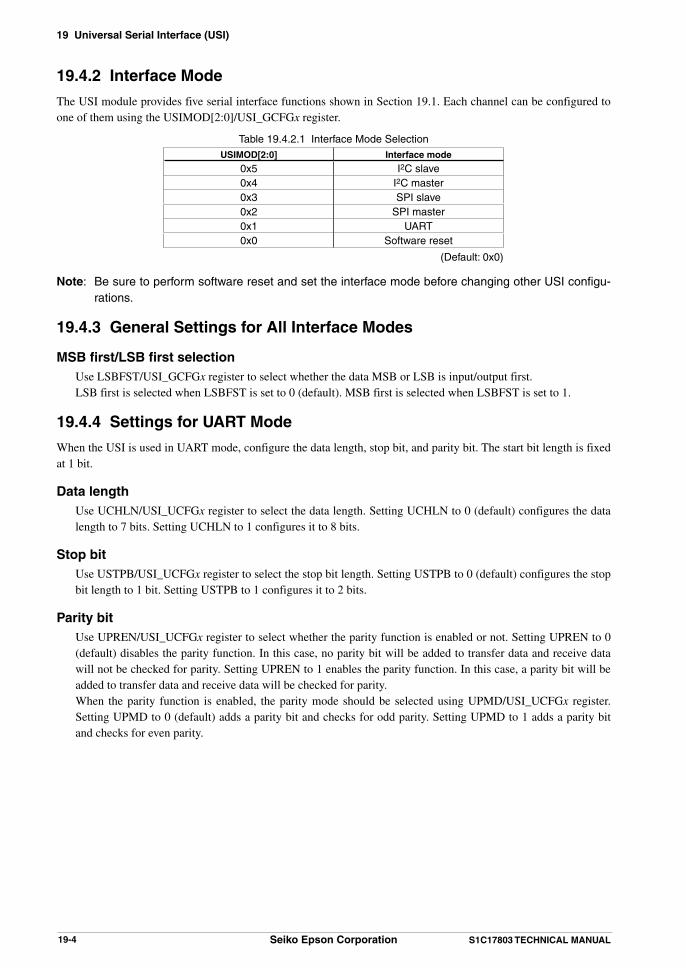
19 Universal Serial Interface (USI)
19-4 Seiko Epson Corporation S1C17803 TECHNICAL MANUAL
19.4.2 Interface Mode
The USI module provides five serial interface functions shown in Section 19.1. Each channel can be configured to one of them using the USIMOD[2:0]/USI_GCFGx register.
Table 19.4.2.1 Interface Mode Selection USIMOD[2:0] Interface mode
0x5 I2C slave0x4 I2C master0x3 SPI slave0x2 SPI master0x1 UART0x0 Software reset
(Default: 0x0)
Note: Be sure to perform software reset and set the interface mode before changing other USI configu-rations.
19.4.3 General Settings for All Interface Modes
MSB first/LSB first selection Use LSBFST/USI_GCFGx register to select whether the data MSB or LSB is input/output first. LSB first is selected when LSBFST is set to 0 (default). MSB first is selected when LSBFST is set to 1.
19.4.4 Settings for UART Mode
When the USI is used in UART mode, configure the data length, stop bit, and parity bit. The start bit length is fixed at 1 bit.
Data length Use UCHLN/USI_UCFGx register to select the data length. Setting UCHLN to 0 (default) configures the data
length to 7 bits. Setting UCHLN to 1 configures it to 8 bits.
Stop bit Use USTPB/USI_UCFGx register to select the stop bit length. Setting USTPB to 0 (default) configures the stop
bit length to 1 bit. Setting USTPB to 1 configures it to 2 bits.
Parity bit Use UPREN/USI_UCFGx register to select whether the parity function is enabled or not. Setting UPREN to 0
(default) disables the parity function. In this case, no parity bit will be added to transfer data and receive data will not be checked for parity. Setting UPREN to 1 enables the parity function. In this case, a parity bit will be added to transfer data and receive data will be checked for parity.
When the parity function is enabled, the parity mode should be selected using UPMD/USI_UCFGx register. Setting UPMD to 0 (default) adds a parity bit and checks for odd parity. Setting UPMD to 1 adds a parity bit and checks for even parity.

19 Universal Serial Interface (USI)
S1C17803 TECHNICAL MANUAL Seiko Epson Corporation 19-5
Sampling clock
UCHLN = 0, UPREN = 0, USTPB = 0
UCHLN = 0, UPREN = 1, USTPB = 0
UCHLN = 0, UPREN = 0, USTPB = 1
UCHLN = 0, UPREN = 1, USTPB = 1
UCHLN = 1, UPREN = 0, USTPB = 0
UCHLN = 1, UPREN = 1, USTPB = 0
UCHLN = 1, UPREN = 0, USTPB = 1
UCHLN = 1, UPREN = 1, USTPB = 1
s1 D0 D1 D2 D3 D4 D5 D6 s2
s1 D0 D1 D2 D3 D4 D5 D6 p s2
s1 D0 D1 D2 D3 D4 D5 D6 s2 s3
s1 D0 D1 D2 D3 D4 D5 D6 p s2 s3
s1 D0 D1 D2 D3 D4 D5 D6 D7 s2
s1 D0 D1 D2 D3 D4 D5 D6 D7 p s2
s1 D0 D1 D2 D3 D4 D5 D6 D7 s2 s3
s1 D0 D1 D2 D3 D4 D5 D6 D7 p s2 s3
s1: start bit, s2 & s3: stop bit, p: parity bit
Figure 19.4.4.1 Transfer Data Format in UART Mode (LSB first)
19.4.5 Settings for SPI Mode
When the USI is used in SPI mode (master or slave), configure the SPI clock polarity/phase and enable/disable the receive data mask function. In SPI master mode, the clock mode and data length should be selected. Note that the data length in SPI slave mode is fixed at 8 bits.
SPI clock polarity and phase settings (master mode and slave mode) Use SCPOL/USI_SCFGx register to select the SPI clock polarity. Setting SCPOL to 1 treats the SPI clock as
active low. Setting it to 0 (default) treats it as active high. The SPI clock phase can be selected using SCPHA/USI_SCFGx register. These control bits set transfer timing as shown in Figure 19.4.5.1.
US_SCKx (SCPOL = 1, SCPHA = 1)
US_SCKx (SCPOL = 1, SCPHA = 0)
US_SCKx (SCPOL = 0, SCPHA = 1)
US_SCKx (SCPOL = 0, SCPHA = 0)
US_SDIx/US_SDOx
Fetching received datainto shift register
D7 (MSB) D0 (LSB)
Figure 19.4.5.1 Clock and Data Transfer Timing (MSB first)
The C17803 does not support the USI-SPI receive data mask function.
Clock mode (master mode only) In SPI master mode, either normal or fast clock mode can be selected using SFSTMOD/USI_SCFGx register.
Setting SFSTMOD to 0 (default) places the USI into normal mode and the USI generates the transfer clock by dividing the T8F output by 2. Setting SFSTMOD to 1 places the USI into fast mode and the USI uses PCLK2 supplied from the CMU directly as the transfer clock. The fast mode does not use the T8F.
The SPI slave mode uses the T8F output clock for generating the sampling clock.

19 Universal Serial Interface (USI)
19-6 Seiko Epson Corporation S1C17803 TECHNICAL MANUAL
Data length (master mode only) In SPI master mode, the data length can be selected using SCHLN/USI_SCFGx register. Setting SCHLN to 0
(default) configures the data length to 8 bits. Setting SCHLN to 1 configures the data length to 9 bits. In 9-bit mode, 8-bit data is prefixed with a command
bit (1 bit). The command bit is used for controlling the SPI LCD controller connected to the USI. The command bit value to be transmitted can be specified using SCMD/USI_SCFGx register. Setting SCMD to 1 configures the command bit to high. Setting SCMD to 0 configures the command bit to low.
SCHLN = 0, SCMD = *
SCHLN = 1, SCMD = 0
SCHLN = 1, SCMD = 1
Command bit
D7 (D0) D6 (D1) D5 (D2) D4 (D3) D3 (D4) D2 (D5) D1 (D6) D0 (D7)
D7 (D0) D6 (D1) D5 (D2) D4 (D3) D3 (D4) D2 (D5) D1 (D6) D0 (D7)
D7 (D0) D6 (D1) D5 (D2) D4 (D3) D3 (D4) D2 (D5) D1 (D6) D0 (D7)
Figure 19.4.5.2 9-bit Transfer Data Format in SPI Master Mode
The data length in SPI slave mode is fixed at 8 bits.
19.4.6 Settings for I2C Mode
The I2C mode does not need to set data format and other conditions. The data length in I2C mode is fixed at 8 bits.
19.5 Data Transfer ControlThis section describes how to control data transfers. The following explanations assume that the configurations de-scribed above and interrupt/DMA settings have already been finished.
19.5.1 Data Transfer in UART Mode
Data transmission To start data transmission in UART mode, write the transmit data to the transmit data buffer (TD[7:0]/USI_TDx
register). The buffer data is sent to the transmit shift register, and the start bit is output from the US_SDOx pin. The data
in the shift register is then output in sequence. Following output of the eighth data bit, the parity bit (if parity is enabled) and the stop bit are output.
The transmitter circuit includes two status flags: UTDIF/USI_UIFx register and UTBSY/USI_UIFx register. The UTDIF flag indicates the transmit data buffer status. This flag is set to 1 indicating that the transmit data
buffer becomes empty when data written to the transmit data buffer is sent to the transmit shift register. UTDIF is an interrupt flag. An interrupt or DMA request can be generated when this flag is set to 1 (see Section 19.7). Write subsequent data to the transmit data buffer to start the following transmission using this interrupt or DMA. The transmit data buffer size is 1 byte, but a shift register is provided separately to allow data to be writ-ten while the previous data is being sent. If an interrupt or DMA is not used for transmission, be sure to confirm that the transmit data buffer is empty before writing transmit data. Writing data before UTDIF has been set will overwrite earlier transmit data inside the transmit data buffer. After UTDIF is set to 1, it can be reset to 0 by writing 1.
The UTBSY flag indicates the shift register status. This flag switches to 1 when transmit data is loaded from the transmit data buffer to the shift register and reverts to 0 once the data is sent. Read this flag to check wheth-er the transmitter circuit is operating or at standby.
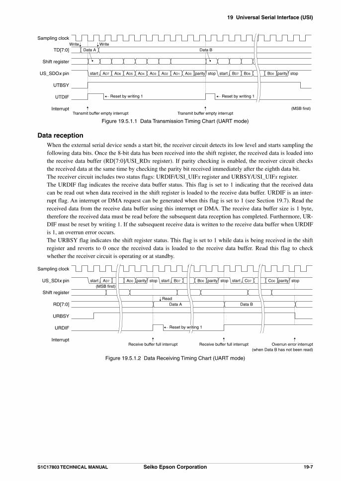
19 Universal Serial Interface (USI)
S1C17803 TECHNICAL MANUAL Seiko Epson Corporation 19-7
Sampling clock
TD[7:0]
Shift register
US_SDOx pin
UTBSY
UTDIF
Interrupt
start stop stopAD7 AD6 AD5 AD4 AD3 AD2 AD1 AD0 parity parityBD0
Write Write
Transmit buffer empty interrupt
Reset by writing 1 Reset by writing 1
Transmit buffer empty interrupt(MSB first)
Data A Data B
start BD7 BD6
Figure 19.5.1.1 Data Transmission Timing Chart (UART mode)
Data reception When the external serial device sends a start bit, the receiver circuit detects its low level and starts sampling the
following data bits. Once the 8-bit data has been received into the shift register, the received data is loaded into the receive data buffer (RD[7:0]/USI_RDx register). If parity checking is enabled, the receiver circuit checks the received data at the same time by checking the parity bit received immediately after the eighth data bit.
The receiver circuit includes two status flags: URDIF/USI_UIFx register and URBSY/USI_UIFx register. The URDIF flag indicates the receive data buffer status. This flag is set to 1 indicating that the received data
can be read out when data received in the shift register is loaded to the receive data buffer. URDIF is an inter-rupt flag. An interrupt or DMA request can be generated when this flag is set to 1 (see Section 19.7). Read the received data from the receive data buffer using this interrupt or DMA. The receive data buffer size is 1 byte, therefore the received data must be read before the subsequent data reception has completed. Furthermore, UR-DIF must be reset by writing 1. If the subsequent receive data is written to the receive data buffer when URDIF is 1, an overrun error occurs.
The URBSY flag indicates the shift register status. This flag is set to 1 while data is being received in the shift register and reverts to 0 once the received data is loaded to the receive data buffer. Read this flag to check whether the receiver circuit is operating or at standby.
Sampling clock
US_SDIx pin
Shift register
RD[7:0]
URBSY
URDIF
Interrupt
start stop stopAD7 parity parity(MSB first)
Data A Data B
start BD7 stopparityAD0 CD0BD0 start CD7
Receive buffer full interrupt Receive buffer full interrupt Overrun error interrupt(when Data B has not been read)
Read
Reset by writing 1
Figure 19.5.1.2 Data Receiving Timing Chart (UART mode)
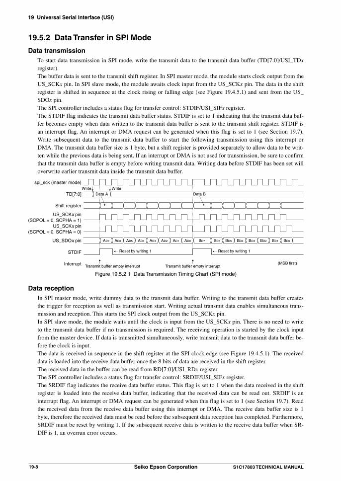
19 Universal Serial Interface (USI)
19-8 Seiko Epson Corporation S1C17803 TECHNICAL MANUAL
19.5.2 Data Transfer in SPI Mode
Data transmission To start data transmission in SPI mode, write the transmit data to the transmit data buffer (TD[7:0]/USI_TDx
register). The buffer data is sent to the transmit shift register. In SPI master mode, the module starts clock output from the
US_SCKx pin. In SPI slave mode, the module awaits clock input from the US_SCKx pin. The data in the shift register is shifted in sequence at the clock rising or falling edge (see Figure 19.4.5.1) and sent from the US_SDOx pin.
The SPI controller includes a status flug for transfer control: STDIF/USI_SIFx register. The STDIF flag indicates the transmit data buffer status. STDIF is set to 1 indicating that the transmit data buf-
fer becomes empty when data written to the transmit data buffer is sent to the transmit shift register. STDIF is an interrupt flag. An interrupt or DMA request can be generated when this flag is set to 1 (see Section 19.7). Write subsequent data to the transmit data buffer to start the following transmission using this interrupt or DMA. The transmit data buffer size is 1 byte, but a shift register is provided separately to allow data to be writ-ten while the previous data is being sent. If an interrupt or DMA is not used for transmission, be sure to confirm that the transmit data buffer is empty before writing transmit data. Writing data before STDIF has been set will overwrite earlier transmit data inside the transmit data buffer.
spi_sck (master mode)
TD[7:0]
Shift register
US_SCKx pin(SCPOL = 0, SCPHA = 1)
US_SCKx pin(SCPOL = 0, SCPHA = 0)
US_SDOx pin
STDIF
Interrupt
AD7 AD6 AD5 AD4 AD3 AD2 AD1 BD5 BD4 BD3 BD2 BD1AD0 BD0
Write Write
Transmit buffer empty interrupt
Reset by writing 1 Reset by writing 1
Transmit buffer empty interrupt(MSB first)
Data A Data B
BD7 BD6
Figure 19.5.2.1 Data Transmission Timing Chart (SPI mode)
Data reception In SPI master mode, write dummy data to the transmit data buffer. Writing to the transmit data buffer creates
the trigger for reception as well as transmission start. Writing actual transmit data enables simultaneous trans-mission and reception. This starts the SPI clock output from the US_SCKx pin.
In SPI slave mode, the module waits until the clock is input from the US_SCKx pin. There is no need to write to the transmit data buffer if no transmission is required. The receiving operation is started by the clock input from the master device. If data is transmitted simultaneously, write transmit data to the transmit data buffer be-fore the clock is input.
The data is received in sequence in the shift register at the SPI clock edge (see Figure 19.4.5.1). The received data is loaded into the receive data buffer once the 8 bits of data are received in the shift register.
The received data in the buffer can be read from RD[7:0]/USI_RDx register. The SPI controller includes a status flug for transfer control: SRDIF/USI_SIFx register. The SRDIF flag indicates the receive data buffer status. This flag is set to 1 when the data received in the shift
register is loaded into the receive data buffer, indicating that the received data can be read out. SRDIF is an interrupt flag. An interrupt or DMA request can be generated when this flag is set to 1 (see Section 19.7). Read the received data from the receive data buffer using this interrupt or DMA. The receive data buffer size is 1 byte, therefore the received data must be read before the subsequent data reception has completed. Furthermore, SRDIF must be reset by writing 1. If the subsequent receive data is written to the receive data buffer when SR-DIF is 1, an overrun error occurs.

19 Universal Serial Interface (USI)
S1C17803 TECHNICAL MANUAL Seiko Epson Corporation 19-9
spi_sck (master mode)
TD[7:0]
US_SCKx pin(SCPOL = 0, SCPHA = 1)
US_SCKx pin(SCPOL = 0, SCPHA = 0)
US_SDIx pin
Shift register
RD[7:0]
SRDIF
Interrupt
AD7 AD6 AD1 AD0 BD1 BD0
Write Write Write
Receive buffer full interrupt Receive buffer full interrupt Overrun error interrupt(when Data B has not been read)
(MSB first)
dummy dummy
Data A Data B
dummy
BD7 BD6 CD1 CD0CD7 CD6
Read
Reset by writing 1
Figure 19.5.2.2 Data Receiving Timing Chart (SPI mode)
Slave select signal In SPI slave mode, data transmission/receiving operations are enabled when the master device's slave select sig-
nal input to the #US_SSIx pin is low. When the slave select signal is high, the SPI controller does not start data transfer even if the clock is input to the US_SCKx pin from the master device.
If a slave select output is required in SPI master mode, use a general-purpose I/O port and control its output with software.
19.5.3 Data Transfer in I2C Mode
overwrite earlier transmit data inside the transmit data buffer.
Master
Slave 1 Slave 2
i2c_scl
i2c_sda
IO1_VDD/IO2_VDD
When the USI is set to I2C, i2c_scl and i2c_sda are in Hi-Z state if not outputting low. (They do not output high level.)For this reason, be sure to externally pull up i2c_scl and i2c_sda to the IO1_VDD/IO2_VDD level.
Note: Be sure to not pull up beyond the IO1_VDD/IO2_VDD level.
Figure 19.5.3.0 I2C Mode Connection Example

19 Universal Serial Interface (USI)
19-10 Seiko Epson Corporation S1C17803 TECHNICAL MANUAL
Control method in I2C master mode Data transfer in I2C master mode is controlled using IMTGMOD[2:0]/USI_IMTGx register and IMTG/USI_
IMTGx register. Select an I2C master operation using IMTGMOD[2:0] and write 1 to IMTG as the trigger. The I2C controller controls the I2C bus to generate the specified operating status.
Table 19.5.3.1 Trigger List in I2C Master Mode IMTGMOD[2:0] Trigger
0x7 Reserved0x6 ACK/NAK reception0x5 NAK transmission0x4 ACK transmission0x3 Data reception0x2 Data transmission0x1 Stop condition0x0 Start condition
(Default: 0x0)
Writing 1 to IMTG sets IMBSY/USI_IMIFx register to 1 indicating that the I2C controller is busy (operating). When the specified operation has finished, IMBSY is reset to 0. At the same time, the interrupt flag (IMIF/USI_IMIFx register) is also set to 1. After an interrupt occurs, read the status bits (IMSTA[2:0]/USI_IMIFx register) to check the operation finished. Then clear IMIF by writing 1. IMSTA[2:0] will be automatically cleared to 0x0.
Figure 19.5.3.2 I2C Master Status BitsIMSTA[2:0] Status
0x7 Reserved0x6 NAK has been received.0x5 ACK has been received.0x4 ACK or NAK has been transmitted.0x3 Receive data buffer is full.0x2 Transmit data buffer is empty.0x1 Stop condition has been generated.0x0 Start condition has been generated.
(Default: 0x0)
Data transmission in I2C master mode The following describes the data transmission procedure in I2C master mode.
START
END
Generate start condition
Generate stop condition
Send slave address and transfer direction bit
ACK received?
yes
ACK received?
yesno
Finished?
yes
Send data
Error handling
no
no
Figure 19.5.3.1 I2C Master Data Transmission Flow Chart

19 Universal Serial Interface (USI)
S1C17803 TECHNICAL MANUAL Seiko Epson Corporation 19-11
Start condition generated ACK receivedTransmit buffer empty
T8F chx output clock
USI_SCKx pin
USI_SDIx (output)
USI_SDIx (input)
IMTGMOD[2:0]
IMTG [write]
IMBSY
IMSTA[2:0]
TD[7:0]
IMIF
Interrupt
* ** Reset by writing 1
Slave address and transfer direction Transfer data 1
0x0 0x2 0x0 0x5 0x0
0x0 0x2 0x6 0x2
ACK
A6 A5 A0 R/W=0 D7 D6
Start conditionAdress transmission
ACK receptionData transmission
(1) Start condition → Data transmission
Stop condition generatedACK received Transmit buffer empty
T8F chx output clock
USI_SCKx pin
USI_SDIx (output)
USI_SDIx (input)
IMTGMOD[2:0]
IMTG[write]
IMBSY
IMSTA[2:0]
TD[7:0]
IMIF
Interrupt
* * ** Reset by writing 1
Transfer data n
0x2 0x0 0x5 0x0 0x1 0x0
0x2 0x6 0x1
ACK
D7 D6 D1 D0
ACK receptionData transmission
ACK reception
ACK received
Transfer data (n-1)
0x0 0x5
ACK
0x6
Stop condition
0x0
(2) Data transmission → Stop condition
Figure 19.5.3.2 I2C Master Data Transmission Timing Chart
(1) Generating start condition I2C data transfer starts when the I2C master device generates a start condition. The start condition applies
when the SCL line is maintained at high and the SDA line is pulled down to low. To generate a start condition in this I2C master, set IMTGMOD[2:0] to 0x0 (default) and write 1 to IMTG.
SDA (US_SDIx)
SCL (US_SCKx)
Start condition
Figure 19.5.3.3 Start Condition
IMBSY is set to 1 while a start condition is being generated. When the start condition is generated, IMBSY is reset to 0 and IMSTA[2:0] is set to 0x0. The I2C bus is busy from this point on.
Note: Other operations cannot be started before a start condition is generated.
(2) Sending slave address and transfer direction bit After a start condition has been generated, send the address of the slave device to be communicated and a
transfer direction bit. I2C slave addresses are either 7-bit or 10-bit. This module uses an 8-bit transfer data buffer to send the slave address and transfer direction bit, enabling single transfers in 7-bit address mode. In 10-bit mode, data is sent twice under software control. Figure 19.5.3.4 shows the configuration of the ad-dress data.

19 Universal Serial Interface (USI)
19-12 Seiko Epson Corporation S1C17803 TECHNICAL MANUAL
Slave address
7-bit address
Transfer direction0: master -> slave (transmission)1: slave -> master (reception)
A6 A5D7 D6
A4D5
A3D4
A2D3
A1D2
A0D1
R/WD0
8 low order slave address bits
A7 A6D7 D6
A5D5
A4D4
A3D3
A2D2
A1D1
A0D0
2 high orderslave address bits
10-bit address
1First transmit data
Second transmit data
1D7 D6
1D5
1D4
0D3
A9D2
A8D1
0D0
2 high orderslave address bits
1Third transmit data 1D7 D6
1D5
1D4
0D3
A9D2
A8D1
1D0
When it is the master which will receive data, issue a repeated start after sending the second transmit data and then, send the third transmit data.
Figure 19.5.3.4 Transmit Data Specifying Slave Address and Transfer Direction
The transfer direction bit indicates the data transfer direction after the slave address has been sent. Set this bit to 0 when sending data from the master to the slave.
To send a slave address, set the address with the transfer direction bit to the transmit data buffer (TD[7:0]/USI_TDx register). Then set IMTGMOD[2:0] to 0x2 and write 1 to IMTG.
To send a 10-bit address, execute this procedure twice as shown in Figure 19.5.3.4. Writing 1 to IMTG sets IMBSY to 1. When data in the transmit data buffer is sent to the transmit shift reg-
ister, IMBSY reverts to 0 and IMSTA[2:0] is set to 0x2. Confirm that the slave address (each byte) has been sent by reading IMBSY or using an interrupt. Data can also be written to the transmit data buffer using DMA.
After a slave address has been sent, the selected slave device sends back an ACK by pulling down the SCL line to low. If the SCL line maintains high, it is regarded as a NAK. In this case, the I2C controller cannot communicate with the slave device specified.
SDA (US_SDIx) (output)
SDA (US_SDIx) (input)
SCL (US_SCKx)
Start condition
1 2 8 9
D7 D6 D0
ACK
NAK
Figure 19.5.3.5 ACK and NAK
It is necessary to check that an ACK has been received before sending data. To do this, set IMTGMOD[2:0] to 0x6 and write 1 to IMTG after the slave address has been sent.
IMBSY is set to 1 while an ACK/NAK is being detected and it reverts to 0 when the detection has com-pleted. Receiving an ACK sets IMSTA[2:0] to 0x5; receiving a NAK sets it to 0x6. Check IMSTA[2:0] after confirming IMBSY or using an interrupt. When an ACK has been received, perform data transmission. When a NAK has been received, perform an error handling.

19 Universal Serial Interface (USI)
S1C17803 TECHNICAL MANUAL Seiko Epson Corporation 19-13
(3) Data transmission The data transmission procedure is the same as that of the slave address transmission. 1. Write an 8-bit transmit data to the transmit data buffer (TD[7:0]). 2. Set IMTGMOD[2:0] to 0x2 and IMTG to 1.
This trigger transfers the buffer data to the transmit shift register to start transmission. The module starts clock output from the US_SCKx pin. The data in the shift register is shifted in sequence with the clock and sent from the US_SDOx pin.
Writing 1 to IMTG sets IMBSY to 1. When data in the transmit data buffer is sent to the transmit shift reg-ister, IMBSY reverts to 0 and IMSTA[2:0] is set to 0x2 (transmit data buffer empty). An interrupt request can be generated at this point. Write subsequent data to the transmit data buffer to start the following trans-mission using this interrupt.
However, as in the case of the slave address transmission, check that the slave device has sent back an ACK (by setting IMTGMOD[2:0] to 0x6 and IMTG to 1) before starting the following 8-bit data transmission.
Repeat an 8-bit data transmission and ACK receiving check for the required number of times.
(4) Generating stop condition To end I2C communication after all data has been sent, the I2C master must generate a stop condition. The
stop condition applies when the SCL line is maintained at high and the SDA line is pulled up from low to high. To generate a stop condition in this I2C master, set IMTGMOD[2:0] to 0x1 and write 1 to IMTG.
Stop condition
SDA (US_SDIx)
SCL (US_SCKx)
Figure 19.5.3.6 Stop Condition
IMBSY is set to 1 while a stop condition is being generated. When the stop condition is generated, IMBSY is reset to 0 and IMSTA[2:0] is set to 0x1. Read IMBSY or use an interrupt to check that a stop condition has been generated. The I2C bus subsequently switches to free state.
(5) Generating repeated start condition To make it possible to continue with a different data transfer after a data transmission has completed, the
I2C master can omit stop condition generation and generate a repeated start condition. To generate a re-peated start condition, perform a start condition generation procedure described in Step (1). Slave address transmission is subsequently possible with the I2C bus remaining in the busy state.
SDA (US_SDIx)
SCL (US_SCKx)
Repeated start condition
Figure 19.5.3.7 Repeated Start Condition

19 Universal Serial Interface (USI)
19-14 Seiko Epson Corporation S1C17803 TECHNICAL MANUAL
Data reception in I2C master mode The following describes the data receiving procedure in I2C master mode.
START
END
Generate start condition
Generate stop condition
Send slave address and transfer direction bit
ACK received?
yes
noFinished?
yes
Receive data
Send ACK
Error handling
no
Figure 19.5.3.8 I2C Master Data Receiving Flow Chart
Start condition generated ACK receivedTransmit buffer empty
T8F chx output clock
USI_SCKx pin
USI_SDIx (output)
USI_SDIx (input)
IMTGMOD[2:0]
IMTG[write]
IMBSY
IMSTA[2:0]
RD[7:0]
IMIF
Interrupt
* ** Reset by writing 1
Slave address and transfer direction
0x0 0x2 0x0 0x5 0x0
0x0 0x2 0x6 0x3
ACK
A6 A5 A0 R/W=1
Start conditionAdress transmission
ACK receptionData reception
D7 D6
(1) Start condition → Data reception
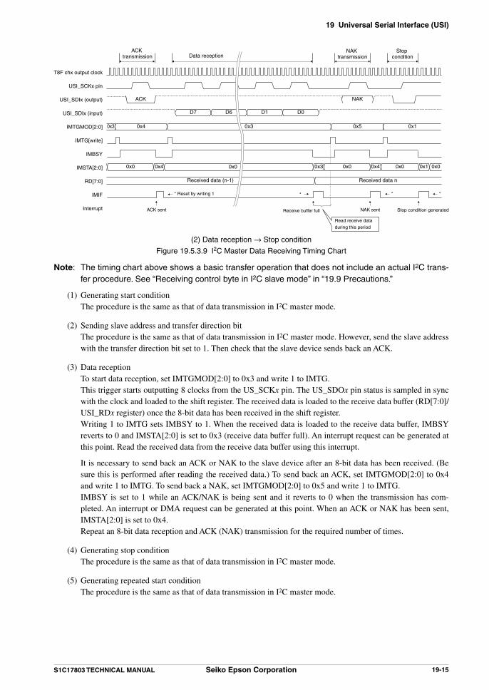
19 Universal Serial Interface (USI)
S1C17803 TECHNICAL MANUAL Seiko Epson Corporation 19-15
Stop condition generatedACK sent Receive buffer full
T8F chx output clock
USI_SCKx pin
USI_SDIx (output)
USI_SDIx (input)
IMTGMOD[2:0]
IMTG[write]
IMBSY
IMSTA[2:0]
RD[7:0]
IMIF
Interrupt
* ** Reset by writing 1
Received data n
*
0x3 0x0 0x4 0x0 0x1 0x0
0x3 0x5 0x1
D7 D6 D1 D0
ACK transmission Data reception
NAK transmission
NAK sent
Received data (n-1)
0x0 0x4
ACK
0x4
Stop condition
0x0
NAK
Read receive data during this period
0x3
(2) Data reception → Stop condition
Figure 19.5.3.9 I2C Master Data Receiving Timing Chart
Note: The timing chart above shows a basic transfer operation that does not include an actual I2C trans-fer procedure. See “Receiving control byte in I2C slave mode” in “19.9 Precautions.”
(1) Generating start condition The procedure is the same as that of data transmission in I2C master mode.
(2) Sending slave address and transfer direction bit The procedure is the same as that of data transmission in I2C master mode. However, send the slave address
with the transfer direction bit set to 1. Then check that the slave device sends back an ACK.
(3) Data reception To start data reception, set IMTGMOD[2:0] to 0x3 and write 1 to IMTG. This trigger starts outputting 8 clocks from the US_SCKx pin. The US_SDOx pin status is sampled in sync
with the clock and loaded to the shift register. The received data is loaded to the receive data buffer (RD[7:0]/USI_RDx register) once the 8-bit data has been received in the shift register.
Writing 1 to IMTG sets IMBSY to 1. When the received data is loaded to the receive data buffer, IMBSY reverts to 0 and IMSTA[2:0] is set to 0x3 (receive data buffer full). An interrupt request can be generated at this point. Read the received data from the receive data buffer using this interrupt.
It is necessary to send back an ACK or NAK to the slave device after an 8-bit data has been received. (Be sure this is performed after reading the received data.) To send back an ACK, set IMTGMOD[2:0] to 0x4 and write 1 to IMTG. To send back a NAK, set IMTGMOD[2:0] to 0x5 and write 1 to IMTG.
IMBSY is set to 1 while an ACK/NAK is being sent and it reverts to 0 when the transmission has com-pleted. An interrupt or DMA request can be generated at this point. When an ACK or NAK has been sent, IMSTA[2:0] is set to 0x4.
Repeat an 8-bit data reception and ACK (NAK) transmission for the required number of times.
(4) Generating stop condition The procedure is the same as that of data transmission in I2C master mode.
(5) Generating repeated start condition The procedure is the same as that of data transmission in I2C master mode.

19 Universal Serial Interface (USI)
19-16 Seiko Epson Corporation S1C17803 TECHNICAL MANUAL
Clock stretch function During transmitting/receiving data, the slave device may issue a wait request to the master device by pulling
down the SCL line to low until the slave device becomes ready to transmit/receive the subsequent data. The master device enters a standby state until the wait request is canceled (the SCL line goes high).
This I2C controller supports this clock stretch function. When a clock stretch condition is detected after a slave address or data has been sent/received, this module enters a waiting status and it does not start operating even if it accepts a trigger for data transfer until the clock stretch status is canceled. IMBSY is maintained at 1 until the triggered operation has completed including a waiting status.
US_SCKx pin (master output)
US_SCKx pin (slave output)
Clock stretch Clock stretch
Figure 19.5.3.10 Clock Stretch
Control method in I2C slave mode Data transfer in I2C slave mode is controlled using ISTGMOD[2:0]/USI_ISTGx register and ISTG/USI_ISTGx
register. Select an I2C slave operation using ISTGMOD[2:0] and write 1 to ISTG as the trigger. The I2C con-troller controls the I2C bus to generate the specified operating status.
Table 19.5.3.3 Trigger List in I2C Slave Mode ISTGMOD[2:0] Trigger
0x7 Reserved0x6 ACK/NAK reception0x5 NAK transmission0x4 ACK transmission0x3 Data reception0x2 Data transmission0x1 Reserved0x0 Wait for start condition
(Default: 0x0)
Writing 1 to ISTG sets ISBSY/USI_ISIFx register to 1 indicating that the I2C controller is busy (operating). When the specified operation has finished, ISBSY is reset to 0. At the same time, the interrupt flag (ISIF/USI_ISIFx register) is also set to 1. After an interrupt occurs, read the status bits (ISSTA[2:0]/USI_ISIFx register) to check the operation finished. Then, write 1 to ISIF to clear. This also automatically clears ISSTA[2:0] to 0x0.
Table 19.5.3.4 I2C Slave Status BitsISSTA[2:0] Status
0x7 Reserved0x6 NAK has been received.0x5 ACK has been received.0x4 ACK or NAK has been transmitted.0x3 Receive data buffer is full.0x2 Transmit data buffer is empty.0x1 Stop condition has been detected.0x0 Start condition has been detected.
(Default: 0x0)

19 Universal Serial Interface (USI)
S1C17803 TECHNICAL MANUAL Seiko Epson Corporation 19-17
Data transmission in I2C slave mode The following describes the data transmission procedure in I2C slave mode.
START
END
Start condition?
Receive slave address and transfer direction bit
Address matched?
yes
ACK received?
yesno
no
yes
Send ACK
Send Data
no
no
yes
Error handlingStop condition?
Figure 19.5.3.11 I2C Slave Data Transmission Flow Chart
Start condition detected ACK sent
T8F chx output clock
USI_SCKx pin
USI_SCKx (input)
USI_SCKx (output)
USI_SDIx (output)
USI_SDIx (input)
ISTGMOD[2:0]
ISTG[write]
ISBSY
ISSTA[2:0]
TD[7:0]
ISIF
Interrupt
* ** Reset by writing 1
0x0 0x3 0x0 0x4 0x0
0x0 0x3 0x4 0x2
ACK
A6 A5 A0 R/W=1
Start condition Address reception
ACK transmission Data transmission
D7 D6
Transfer data 1
Receive buffer full
Read receive data during this period
(1) Start condition → Data transmission
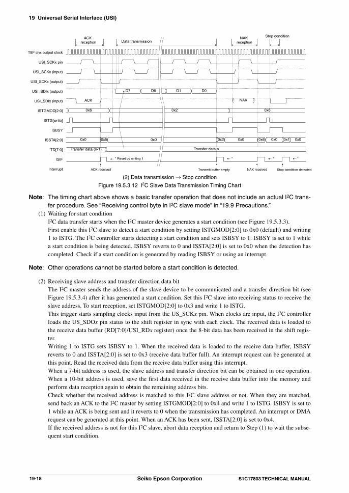
19 Universal Serial Interface (USI)
19-18 Seiko Epson Corporation S1C17803 TECHNICAL MANUAL
Stop condition detectedNAK received
T8F chx output clock
USI_SCKx pin
USI_SCKx (input)
USI_SCKx (output)
USI_SDIx (output)
USI_SDIx (input)
ISTGMOD[2:0]
ISTG[write]
ISBSY
ISSTA[2:0]
TD[7:0]
ISIF
Interrupt
** ** Reset by writing 1
0x0 0x5 0x2 0x0
0x2 0x6
D7 D6 D1 D0
Data transmissionNAK
reception
Transfer data n
Transmit buffer empty
ACK reception
Stop condition
NAKACK
0x6
0x0 0x10x6 0x00x0
Transfer data (n-1)
ACK received
(2) Data transmission → Stop condition
Figure 19.5.3.12 I2C Slave Data Transmission Timing Chart
Note: The timing chart above shows a basic transfer operation that does not include an actual I2C trans-fer procedure. See “Receiving control byte in I2C slave mode” in “19.9 Precautions.”
(1) Waiting for start condition I2C data transfer starts when the I2C master device generates a start condition (see Figure 19.5.3.3). First enable this I2C slave to detect a start condition by setting ISTGMOD[2:0] to 0x0 (default) and writing
1 to ISTG. The I2C controller starts detecting a start condition and sets ISBSY to 1. ISBSY is set to 1 while a start condition is being detected. ISBSY reverts to 0 and ISSTA[2:0] is set to 0x0 when the detection has completed. Check if a start condition is generated by reading ISBSY or using an interrupt.
Note: Other operations cannot be started before a start condition is detected.
(2) Receiving slave address and transfer direction data bit The I2C master sends the address of the slave device to be communicated and a transfer direction bit (see
Figure 19.5.3.4) after it has generated a start condition. Set this I2C slave into receiving status to receive the slave address. To start reception, set ISTGMOD[2:0] to 0x3 and write 1 to ISTG.
This trigger starts sampling clocks input from the US_SCKx pin. When clocks are input, the I2C controller loads the US_SDOx pin status to the shift register in sync with each clock. The received data is loaded to the receive data buffer (RD[7:0]/USI_RDx register) once the 8-bit data has been received in the shift regis-ter.
Writing 1 to ISTG sets ISBSY to 1. When the received data is loaded to the receive data buffer, ISBSY reverts to 0 and ISSTA[2:0] is set to 0x3 (receive data buffer full). An interrupt request can be generated at this point. Read the received data from the receive data buffer using this interrupt.
When a 7-bit address is used, the slave address and transfer direction bit can be obtained in one operation. When a 10-bit address is used, save the first data received in the receive data buffer into the memory and perform data reception again to obtain the remaining address bits.
Check whether the received address is matched to this I2C slave address or not. When they are matched, send back an ACK to the I2C master by setting ISTGMOD[2:0] to 0x4 and write 1 to ISTG. ISBSY is set to 1 while an ACK is being sent and it reverts to 0 when the transmission has completed. An interrupt or DMA request can be generated at this point. When an ACK has been sent, ISSTA[2:0] is set to 0x4.
If the received address is not for this I2C slave, abort data reception and return to Step (1) to wait the subse-quent start condition.

19 Universal Serial Interface (USI)
S1C17803 TECHNICAL MANUAL Seiko Epson Corporation 19-19
(3) Data transmission When the transfer direction bit received with the slave address in Step (2) is 1, start data transmission by the
following procedure: 1. Write an 8-bit transmit data to the transmit data buffer (TD[7:0]). 2. Set ISTGMOD[2:0] to 0x2 and ISTG to 1.
This trigger transfers the buffer data to the transmit shift register to start transmission. When clocks are in-put from the US_SCKx pin, the data in the shift register is shifted in sequence with the clock and sent from the US_SDOx pin.
Writing 1 to ISTG sets ISBSY to 1. When data in the transmit data buffer is sent to the transmit shift regis-ter, ISBSY reverts to 0 and ISSTA[2:0] is set to 0x2 (transmit data buffer empty). An interrupt or DMA re-quest can be generated at this point. Write subsequent data to the transmit data buffer to start the following transmission using this interrupt or DMA.
However, check that the master device has sent back an ACK or NAK (by setting ISTGMOD[2:0] to 0x6 and ISTG to 1) before starting the following 8-bit data transmission.
ISBSY is set to 1 while an ACK/NAK is being detected and it reverts to 0 when the detection has complet-ed. Receiving an ACK sets ISSTA[2:0] to 0x5; receiving a NAK sets it to 0x6. Check ISSTA[2:0] after con-firming ISBSY or using an interrupt. When an ACK has been received, perform data transmission. When a NAK has been received, perform the appropriate handling.
(4) When a stop condition is received If the ISSTA[2:0] value read during data transmission is 0x1, the I2C master device has generated a stop
condition (see Figure 19.5.3.6). In this case, abort data transmission. The stop condition can also be received when ISTGMOD[2:0] is set to one of the modes below. If the stop condition shown in Figure 19.5.3.6 occurs in any of these modes after writing 1 to ISTG, the I2C
slave detects the stop condition.
ISTGMOD[2:0]= 0x2 (Data transmission) 0x3 (Data reception) 0x5 (NAK transmission) 0x6 (ACK/NAK reception)
Data reception in I2C slave mode The following describes the data receiving procedure in I2C slave mode.
START
END
no
Receive data
Send ACK
Start condition?
Stop condition?
Receive slave address and transfer direction bit
Address matched?
yes
yes
Send ACK
no
no
yes
Figure 19.5.3.13 I2C Slave Data Receiving Flow Chart

19 Universal Serial Interface (USI)
19-20 Seiko Epson Corporation S1C17803 TECHNICAL MANUAL
Start condition detected ACK sent
T8F chx output clock
USI_SCKx pin
USI_SCKx (input)
USI_SCKx (output)
USI_SDIx (output)
USI_SDIx (input)
ISTGMOD[2:0]
ISTG[write]
ISBSY
ISSTA[2:0]
RD[7:0]
ISIF
Interrupt
* ** Reset by writing 1
0x0 0x3 0x0 0x4 0x0
0x0 0x3 0x4 0x3
ACK
A6 A5 A0 R/W=0
Start condition Address reception
ACK transmission
Data reception
D7 D6
Slave address
Receive buffer full
Read receive data during this period
(1) Start condition → Data reception
Stop condition detectedNAK sent
T8F chx output clock
USI_SCKx pin
USI_SCKx (input)
USI_SCKx (output)
USI_SDIx (output)
USI_SDIx (input)
ISTGMOD[2:0]
ISTG[write]
ISBSY
ISSTA[2:0]
RD[7:0]
ISIF
Interrupt
** ** Reset by writing 1
0x0 0x4 0x3 0x
0x6
D7 D6 D1 D0
Data reception NAK reception
Transfer data n
ACK receptionStop condition
NAKACK
0x4
0x0 0x0x4 0x00x0
Transfer data (n-1)
ACK sentReceive buffer full
Read receive data during this period
0x3
(2) Data reception → Stop condition
Figure 19.5.3.14 I2C Slave Data Receiving Timing Chart
Note: The timing chart above shows a basic transfer operation that does not include an actual I2C trans-fer procedure. See “Receiving control byte in I2C slave mode” in “19.9 Precautions.”
(1) Waiting for start condition The procedure is the same as that of data transmission in I2C slave mode.
(2) Receiving slave address and transfer direction data bit The procedure is the same as that of data transmission in I2C slave mode.
(3) Data reception When the transfer direction bit received with the slave address in Step (2) is 0, start data reception by set-
ting ISTGMOD[2:0] to 0x3 and writing 1 to ISTG. When clocks are input, the I2C controller loads the US_SDOx pin status to the shift register in sync with
each clock. The received data is loaded to the receive data buffer (RD[7:0]/USI_RDx register) once the 8-bit data has been received in the shift register.

19 Universal Serial Interface (USI)
S1C17803 TECHNICAL MANUAL Seiko Epson Corporation 19-21
Writing 1 to ISTG sets ISBSY to 1. When the received data is loaded to the receive data buffer, ISBSY re-verts to 0 and ISSTA[2:0] is set to 0x3 (receive data buffer full). An interrupt or DMA request can be gener-ated at this point. Read the received data from the receive data buffer using this interrupt or DMA.
It is necessary to send back an ACK or NAK to the master device after an 8-bit data has been received. (Be sure this is performed after reading the received data.) To send back an ACK, set ISTGMOD[2:0] to 0x4 and write 1 to ISTG. To send back a NAK, set ISTGMOD[2:0] to 0x5 and write 1 to ISTG.
ISBSY is set to 1 while an ACK/NAK is being sent and it reverts to 0 when the transmission has completed. An interrupt or DMA request can be generated at this point. When an ACK or NAK has been sent, ISSTA[2:0] is set to 0x4.
Repeat an 8-bit data reception and ACK (NAK) transmission for the required number of times.
(4) When a stop condition is received If the ISSTA[2:0] value read during data reception is 0x1, the I2C master device has generated a stop condi-
tion (see Figure 19.5.3.6). In this case, abort data reception. The stop condition can also be received when ISTGMOD[2:0] is set to one of the modes below. If the stop condition shown in Figure 19.5.3.6 occurs in any of these modes after writing 1 to ISTG, the I2C
slave detects the stop condition.
ISTGMOD[2:0]= 0x2 (Data transmission) 0x3 (Data reception) 0x5 (NAK transmission) 0x6 (ACK/NAK reception)
Clock stretch function While data is being sent/received, this I2C slave generates a clock stretch status by pulling down the SCL line to
low to make a wait request to the master device after an ACK is sent/received until the following data transfer is started.
19.6 Receive ErrorsIn UART mode, three different receive errors (overrun error, framing error, and parity error) may be detected while receiving data. In SPI master and I2C modes, overrun errors may be detected while receiving data.Since receive errors are interrupt causes, they can be processed by generating interrupts. For more information on interrupt control, see Section 19.7.
Overrun error (all interface modes) If data is received before the previously received data in the receive data buffer has not been read, the receive
data buffer is overwritten and an overrun error occurs. When an overrun error occurs, the overrun error flag for the current interface mode is set to 1.
Overrun error flags: UOEIF/USI_UIFx register (UART mode) SEIF/USI_SIFx register (SPI master) IMEIF/USI_IMIFx register (I2C master mode) ISEIF/USI_ISIFx register (I2C slave mode)
The receiving operation continues even if this error occurs. The overrun error flag is reset to 0 by writing 1.
Framing error (UART mode only) If the stop bit is received as 0 in UART mode, the UART controller determines loss of sync and a framing error
occurs. If the stop bit is configured to two bits, only the first bit is checked. The framing error flag (USEIF/USI_UIFx register) is set to 1 if this error occurs. The received data is still trans-
ferred to the receive data buffer if this error occurs and the receiving operation continues, but the data cannot be guaranteed, even if no framing error occurs for subsequent data receiving. The framing error flag is reset to 0
by writing 1.
19 Universal Serial Interface (USI)
19-22 Seiko Epson Corporation S1C17803 TECHNICAL MANUAL
Parity error (UART mode only) If UPREN/USI_UCFGx register has been set to 1 (parity enabled), data received is checked for parity in UART
mode. Data received in the shift register is checked for parity when sent to the receive data buffer. The match-ing is checked against the UPMD/USI_UCFGx register setting (odd or even parity). If the result is a non-match, a parity error is issued, and the parity error flag (UPEIF/USI_UIFx register) is set to 1. Even if this error occurs, the data received is sent to the receive data buffer, and the receiving operation continues. However, the received data cannot be guaranteed if a parity error occurs. The UPEIF flag is reset to 0 by writing 1.
19.7 USI Interrupts and DMAThis section describes the USI interrupts generated in each interface mode and invoking DMA.For more information on interrupt processing and DMA transfer, see the “Interrupt Controller (ITC)” chapter and the “DMA Controller (DMAC)” chapter, respectively.
Each USI channel outputs one interrupt signal (two signals for two channels) shared by the all interrupt causes to the interrupt controller (ITC). Inspect the interrupt flags available in each mode to determine the interrupt cause oc-curred.
19.7.1 Interrupts in UART Mode
The UART mode includes a function for generating the following three different types of interrupts.• Transmit buffer empty interrupt• Receive buffer full interrupt• Receive error interrupt
Transmit buffer empty interrupt To use this interrupt, set UTDIE/USI_UIEx register to 1. If UTDIE is set to 0 (default), interrupt requests for
this cause will not be sent to the ITC. When transmit data written to the transmit data buffer is transferred to the shift register, the USI module sets
UTDIF/USI_UIFx register to 1, indicating that the transmit data buffer is empty. If transmit buffer empty inter-rupts are enabled (UTDIE = 1), an interrupt request is sent simultaneously to the ITC. An interrupt occurs if other interrupt conditions are met. You can inspect the UTDIF flag in the interrupt handler routine to determine whether the USI (UART mode) interrupt is attributable to a transmit buffer empty. If UTDIF is 1, the next trans-mit data can be written to the transmit data buffer by the interrupt handler routine.
Receive buffer full interrupt To use this interrupt, set URDIE/USI_UIEx register to 1. If URDIE is set to 0 (default), interrupt requests for
this cause will not be sent to the ITC. If a received data is loaded into the receive data buffer, the USI module sets URDIF/USI_UIFx register to 1.
If receive buffer full interrupts are enabled (URDIE = 1), an interrupt request is sent simultaneously to the ITC. An interrupt occurs if other interrupt conditions are met. You can inspect the URDIF flag in the interrupt handler routine to determine whether the USI (UART mode) interrupt is attributable to a receive buffer full. If URDIF is 1, the received data can be read from the receive data buffer by the interrupt handler routine. However, be sure to check whether a receive error has occurred or not.
Receive error interrupt To use this interrupt, set UEIE/USI_UIEx register to 1. If UEIE is set to 0 (default), interrupt requests for this
cause will not be sent to the ITC. The USI module sets an error flag (UPEIF/USI_UIFx register, USEIF/USI_UIFx register, or UOEIF/USI_UIFx
register) to 1 if a parity error, framing error, or overrun error is detected when receiving data. If receive error interrupts are enabled (UEIE = 1), an interrupt request is sent simultaneously to the ITC. If other interrupt con-ditions are satisfied, an interrupt occurs. You can inspect the UPEIF, USEIF, and UOEIF flags in the interrupt handler routine to determine whether the USI (UART mode) interrupt was caused by a receive error. If any of the error flags has the value 1, the interrupt handler routine will proceed with error recovery.
To reset an overrun error, initialize USI by performing a USI software reset (USI_CGFGx[D2-0]=0x0).

19 Universal Serial Interface (USI)
S1C17803 TECHNICAL MANUAL Seiko Epson Corporation 19-23
19.7.2 Interrupts in SPI Mode
The SPI master/slave modes include a function for generating the following three different types of interrupts.• Transmit buffer empty interrupt• Receive buffer full interrupt• Receive error interrupt (master mode)
Transmit buffer empty interrupt To use this interrupt, set STDIE/USI_SIEx register to 1. If STDIE is set to 0 (default), interrupt requests for this
cause will not be sent to the ITC. When transmit data written to the transmit data buffer is transferred to the shift register, the USI module sets
STDIF/USI_SIFx register to 1, indicating that the transmit data buffer is empty. If transmit buffer empty inter-rupts are enabled (STDIE = 1), an interrupt request is sent simultaneously to the ITC. An interrupt occurs if other interrupt conditions are met. You can inspect the STDIF flag in the interrupt handler routine to determine whether the USI (SPI master/slave mode) interrupt is attributable to a transmit buffer empty. If STDIF is 1, the next transmit data can be written to the transmit data buffer by the interrupt handler routine.
Receive buffer full interrupt To use this interrupt, set SRDIE/USI_SIEx register to 1. If SRDIE is set to 0 (default), interrupt requests for this
cause will not be sent to the ITC. If a received data is loaded into the receive data buffer, the USI module sets SRDIF/USI_SIFx register to 1. If
receive buffer full interrupts are enabled (SRDIE = 1), an interrupt request is sent simultaneously to the ITC. An interrupt occurs if other interrupt conditions are met. You can inspect the SRDIF flag in the interrupt han-dler routine to determine whether the USI (SPI master/slave mode) interrupt is attributable to a receive buffer full. If SRDIF is 1, the received data can be read from the receive data buffer by the interrupt handler routine. However, be sure to check whether a receive error has occurred or not.
Receive error interrupt To use this interrupt, set SEIE/USI_SIEx register to 1. If SEIE is set to 0 (default), interrupt requests for this
cause will not be sent to the ITC. The USI module sets SEIF/USI_SIFx register to 1 if an overrun error is detected when receiving data. If receive
error interrupts are enabled (SEIE = 1), an interrupt request is sent simultaneously to the ITC. An interrupt occurs if other interrupt conditions are met. You can inspect the SEIF flags in the interrupt handler routine to determine whether the USI (SPI master) interrupt was caused by a receive error. If SEIF is 1, the interrupt han-dler routine will proceed with error recovery. To reset an overrun error, read the receive data buffer (USI_RDx) twice after clearing the flag.
19.7.3 Interrupts in I2C Master Mode
The I2C master mode includes a function for generating the following two different types of interrupts.• Operation completion interrupt• Receive error interrupt
Operation completion interrupt To use this interrupt, set IMIE/USI_IMIEx register to 1. If IMIE is set to 0 (default), interrupt requests for this
cause will not be sent to the ITC. When the operation that initiated by a software trigger has completed, the USI module sets IMIF/USI_IMIFx
register to 1. If operation completion interrupts are enabled (IMIE = 1), an interrupt request is sent simultane-ously to the ITC. An interrupt occurs if other interrupt conditions are met. You can inspect the IMSTA[2:0]/USI_IMIFx register in the interrupt handler routine to determine the I2C operation/status that causes the inter-rupt.

19 Universal Serial Interface (USI)
19-24 Seiko Epson Corporation S1C17803 TECHNICAL MANUAL
Table 19.7.3.1 I2C Master Status BitsIMSTA[2:0] Status
0x7 Reserved0x6 NAK has been received.0x5 ACK has been received.0x4 ACK or NAK has been transmitted.0x3 Receive data buffer is full.0x2 Transmit data buffer is empty.0x1 Stop condition has been generated.0x0 Start condition has been generated.
(Default: 0x0)
Receive error interrupt An overrun error occurs if the trigger for transmission or reception is fired when there are 2 bytes of received
data that has yet to be read. If an overrun error occurs, clear the IMEIF/ISEIF flag and read out the receive buf-fer twice.
To use this interrupt, set IMEIE/USI_IMIEx register to 1. If IMEIE is set to 0 (default), interrupt requests for this cause will not be sent to the ITC.
The USI module sets IMEIF/USI_IMIFx register to 1 if an overrun error is detected when receiving data. If receive error interrupts are enabled (IMEIE = 1), an interrupt request is sent simultaneously to the ITC. An interrupt occurs if other interrupt conditions are met. You can inspect the IMEIF flags in the interrupt handler routine to determine whether the USI (I2C master mode) interrupt was caused by a receive error. If IMEIF is 1, the interrupt handler routine will proceed with error recovery.
19.7.4 Interrupts in I2C Slave Mode
The I2C slave mode includes a function for generating the following two different types of interrupts.• Operation completion interrupt• Receive error interrupt
Operation completion interrupt To use this interrupt, set ISIE/USI_ISIEx register to 1. If ISIE is set to 0 (default), interrupt requests for this
cause will not be sent to the ITC. When the operation that initiated by a software trigger has completed, the USI module sets ISIF/USI_ISIFx reg-
ister to 1. If operation completion interrupts are enabled (ISIE = 1), an interrupt request is sent simultaneously to the ITC. An interrupt occurs if other interrupt conditions are met. You can inspect the ISSTA[2:0]/USI_ISIFx register in the interrupt handler routine to determine the I2C operation/status that causes the interrupt.
Table 19.7.4.1 I2C Slave Status BitsISSTA[2:0] Status
0x7 Reserved0x6 NAK has been received.0x5 ACK has been received.0x4 ACK or NAK has been transmitted.0x3 Receive data buffer is full.0x2 Transmit data buffer is empty.0x1 Stop condition has been detected.0x0 Start condition has been detected.
(Default: 0x0)

19 Universal Serial Interface (USI)
S1C17803 TECHNICAL MANUAL Seiko Epson Corporation 19-25
Receive error interrupt To use this interrupt, set ISEIE/USI_ISIEx register to 1. If ISEIE is set to 0 (default), interrupt requests for this
cause will not be sent to the ITC. The USI module sets ISEIF/USI_ISIFx register to 1 if an overrun error is detected when receiving data. If re-
ceive error interrupts are enabled (ISEIE = 1), an interrupt request is sent simultaneously to the ITC. An inter-rupt occurs if other interrupt conditions are met. You can inspect the ISEIF flags in the interrupt handler routine to determine whether the USI (I2C slave mode) interrupt was caused by a receive error. If ISEIF is 1, the inter-rupt handler routine will proceed with error recovery.
19.7.5 111DMA Transfer
The causes of receive buffer full and transmit buffer empty interrupts in UART and SPI master/slave modes can invoke a DMA. This allows continuous data transmission/reception through DMA transfer between memory and transmit/receive data buffers. These interrupt signals are output to both the ITC and DMAC. Therefore, DMA trans-fer can be performed without generating any USI interrupt.The following lists the DMAC channels that allow selection of a USI interrupt cause as the trigger.
USI Ch.0 receive buffer full: DMAC Ch.0USI Ch.0 transmit buffer empty: DMAC Ch.1USI Ch.1 receive buffer full: DMAC Ch.2USI Ch.1 transmit buffer empty: DMAC Ch.3
For more information on DMA transfer, see the “DMA Controller (DMAC)” chapter.
Note: The USI module cannot invoke a DMA in I2C master and slave mode.
19.8 Control Register DetailsTable 19.8.1 List of USI Registers
Address Register name Function0x80500 USI_GCFG0 USI Ch.0 Global Configuration Register Sets interface and MSB/LSB mode.0x80501 USI_TD0 USI Ch.0 Transmit Data Buffer Register Transmit data buffer0x80502 USI_RD0 USI Ch.0 Receive Data Buffer Register Receive data buffer0x80540 USI_UCFG0 USI Ch.0 UART Mode Configuration Register Sets UART transfer conditions.0x80541 USI_UIE0 USI Ch.0 UART Mode Interrupt Enable Register Enables interrupts.0x80542 USI_UIF0 USI Ch.0 UART Mode Interrupt Flag Register Indicates interrupt occurrence status.0x80550 USI_SCFG0 USI Ch.0 SPI Master/Slave Mode Configuration Register Sets SPI transfer conditions.0x80551 USI_SIE0 USI Ch.0 SPI Master/Slave Mode Interrupt Enable Register Enables interrupts.0x80552 USI_SIF0 USI Ch.0 SPI Master/Slave Mode Interrupt Flag Register Indicates interrupt occurrence status.0x80560 USI_IMTG0 USI Ch.0 I2C Master Mode Trigger Register Starts I2C master operations.0x80561 USI_IMIE0 USI Ch.0 I2C Master Mode Interrupt Enable Register Enables interrupts.0x80562 USI_IMIF0 USI Ch.0 I2C Master Mode Interrupt Flag Register Indicates interrupt occurrence status.0x80570 USI_ISTG0 USI Ch.0 I2C Slave Mode Trigger Register Starts I2C slave operations.0x80571 USI_ISIE0 USI Ch.0 I2C Slave Mode Interrupt Enable Register Enables interrupts.0x80572 USI_ISIF0 USI Ch.0 I2C Slave Mode Interrupt Flag Register Indicates interrupt occurrence status.0x80600 USI_GCFG1 USI Ch.1 Global Configuration Register Sets interface and MSB/LSB mode.0x80601 USI_TD1 USI Ch.1 Transmit Data Buffer Register Transmit data buffer0x80602 USI_RD1 USI Ch.1 Receive Data Buffer Register Receive data buffer0x80640 USI_UCFG1 USI Ch.1 UART Mode Configuration Register Sets UART transfer conditions.0x80641 USI_UIE1 USI Ch.1 UART Mode Interrupt Enable Register Enables interrupts.0x80642 USI_UIF1 USI Ch.1 UART Mode Interrupt Flag Register Indicates interrupt occurrence status.0x80650 USI_SCFG1 USI Ch.1 SPI Master/Slave Mode Configuration Register Sets SPI transfer conditions.0x80651 USI_SIE1 USI Ch.1 SPI Master/Slave Mode Interrupt Enable Register Enables interrupts.0x80652 USI_SIF1 USI Ch.1 SPI Master/Slave Mode Interrupt Flag Register Indicates interrupt occurrence status.0x80660 USI_IMTG1 USI Ch.1 I2C Master Mode Trigger Register Starts I2C master operations.0x80661 USI_IMIE1 USI Ch.1 I2C Master Mode Interrupt Enable Register Enables interrupts.0x80662 USI_IMIF1 USI Ch.1 I2C Master Mode Interrupt Flag Register Indicates interrupt occurrence status.0x80670 USI_ISTG1 USI Ch.1 I2C Slave Mode Trigger Register Starts I2C slave operations.0x80671 USI_ISIE1 USI Ch.1 I2C Slave Mode Interrupt Enable Register Enables interrupts.0x80672 USI_ISIF1 USI Ch.1 I2C Slave Mode Interrupt Flag Register Indicates interrupt occurrence status.
The USI registers are described in detail below. These are 8-bit registers.Note: When data is written to the registers, the “Reserved” bits must always be written as 0 and not 1.
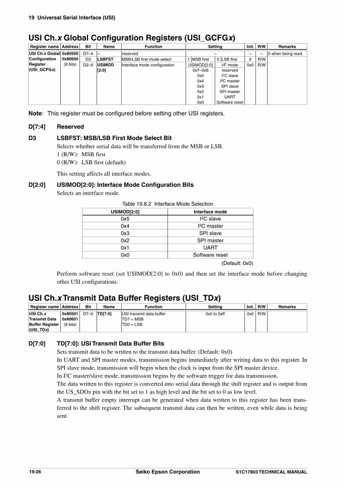
19 Universal Serial Interface (USI)
19-26 Seiko Epson Corporation S1C17803 TECHNICAL MANUAL
USI Ch.x Global Configuration Registers (USI_GCFGx)Register name Address Bit Name Function Setting Init. R/W Remarks
USI Ch.x Global Configuration Register (USI_GCFGx)
0x805000x80600(8 bits)
D7–4 – reserved – – – 0 when being read.D3 LSBFST MSB/LSB first mode select 1 MSB first 0 LSB first 0 R/W
D2–0 USIMOD[2:0]
Interface mode configuration USIMOD[2:0] I/F mode 0x0 R/W0x7–0x6
0x50x40x30x20x10x0
reservedI2C slave
I2C masterSPI slave
SPI masterUART
Software reset
Note: This register must be configured before setting other USI registers.
D[7:4] Reserved
D3 LSBFST: MSB/LSB First Mode Select Bit Selects whether serial data will be transferred from the MSB or LSB. 1 (R/W): MSB first 0 (R/W): LSB first (default)
This setting affects all interface modes.
D[2:0] USIMOD[2:0]: Interface Mode Configuration Bits Selects an interface mode.
Table 19.8.2 Interface Mode Selection USIMOD[2:0] Interface mode
0x5 I2C slave0x4 I2C master0x3 SPI slave0x2 SPI master0x1 UART0x0 Software reset
(Default: 0x0)
Perform software reset (set USIMOD[2:0] to 0x0) and then set the interface mode before changing other USI configurations.
USI Ch.x Transmit Data Buffer Registers (USI_TDx)Register name Address Bit Name Function Setting Init. R/W Remarks
USI Ch.x Transmit Data Buffer Register (USI_TDx)
0x805010x80601(8 bits)
D7–0 TD[7:0] USI transmit data bufferTD7 = MSBTD0 = LSB
0x0 to 0xff 0x0 R/W
D[7:0] TD[7:0]: USI Transmit Data Buffer Bits Sets transmit data to be written to the transmit data buffer. (Default: 0x0) In UART and SPI master modes, transmission begins immediately after writing data to this register. In
SPI slave mode, transmission will begin when the clock is input from the SPI master device. In I2C master/slave mode, transmission begins by the software trigger for data transmission. The data written to this register is converted into serial data through the shift register and is output from
the US_SDOx pin with the bit set to 1 as high level and the bit set to 0 as low level. A transmit buffer empty interrupt can be generated when data written to this register has been trans-
ferred to the shift register. The subsequent transmit data can then be written, even while data is being sent.

19 Universal Serial Interface (USI)
S1C17803 TECHNICAL MANUAL Seiko Epson Corporation 19-27
USI Ch.x Receive Data Buffer Registers (USI_RDx)Register name Address Bit Name Function Setting Init. R/W Remarks
USI Ch.x Receive Data Buffer Register (USI_RDx)
0x805020x80602(8 bits)
D7–0 RD[7:0] USI receive data bufferRD7 = MSBRD0 = LSB
0x0 to 0xff 0x0 R
D[7:0] RD[7:0]: USI Receive Data Buffer Bits Contains the received data. (Default: 0x0) Serial data input from the US_SDIx pin is converted to parallel, with the high level bit set to 1 and the
low level bit set to 0, and then it is loaded to this register. A receive buffer full interrupt can be generated when the data received in the shift register has been
loaded to this register. Data can then be read until subsequent data is received. If receiving the subse-quent data is completed before the register has been read out, the new received data overwrites the con-tents.
This register is read-only.
USI Ch.x UART Mode Configuration Registers (USI_UCFGx)Register name Address Bit Name Function Setting Init. R/W Remarks
USI Ch.x UART Mode Configuration Register (USI_UCFGx)
0x805400x80640(8 bits)
D7–4 – reserved – – – 0 when being read.D3 UCHLN Character length select 1 8 bits 0 7 bits 0 R/WD2 USTPB Stop bit select 1 2 bits 0 1 bit 0 R/WD1 UPMD Parity mode select 1 Even 0 Odd 0 R/WD0 UPREN Parity enable 1 With parity 0 No parity 0 R/W
Note: This register is effective only in UART mode. Configure the USI channel to UART mode before setting this register.
D[7:4] Reserved
D3 UCHLN: Character Length Select Bit Selects the serial transfer data length. 1 (R/W): 8 bits 0 (R/W): 7 bits (default)
When 7-bit data length is selected, D7 in the transmit data buffer is ignored and D7 in the receive data buffer is always set to 0.
D2 USTPB: Stop Bit Select Bit Selects the stop bit length. 1 (R/W): 2 bits 0 (R/W): 1 bit (default)
Writing 1 to USTPB selects 2 stop bits; writing 0 to it selects 1 bit. The start bit is fixed at 1 bit.
D1 UPMD: Parity Mode Select Bit Selects the parity mode. 1 (R/W): Even parity 0 (R/W): Odd parity (default)
Parity checking and parity bit addition are enabled only when UPREN is set to 1. The UPMD setting is disabled if UPREN is 0.
D0 UPREN: Parity Enable Bit Enables the parity function. 1 (R/W): With parity 0 (R/W): No parity (default)
UPREN is used to select whether received data parity checking is performed and whether a parity bit is added to transmit data. Setting UPREN to 1 parity-checks the received data. A parity bit is automati-cally added to the transmit data. If UPREN is set to 0, no parity bit is checked or added.

19 Universal Serial Interface (USI)
19-28 Seiko Epson Corporation S1C17803 TECHNICAL MANUAL
USI Ch.x UART Mode Interrupt Enable Registers (USI_UIEx)Register name Address Bit Name Function Setting Init. R/W Remarks
USI Ch.x UART Mode Interrupt Enable Register (USI_UIEx)
0x805410x80641(8 bits)
D7–3 – reserved – – – 0 when being read.D2 UEIE Receive error interrupt enable 1 Enable 0 Disable 0 R/WD1 URDIE Receive buffer full interrupt enable 1 Enable 0 Disable 0 R/WD0 UTDIE Transmit buffer empty int. enable 1 Enable 0 Disable 0 R/W
Note: This register is effective only in UART mode. Configure the USI channel to UART mode before this register can be used.
D[7:3] Reserved
D2 UEIE: Receive Error Interrupt Enable Bit Enables interrupt requests to the ITC when a receive error occurs. 1 (R/W): Enabled 0 (R/W): Disabled (default)
Set this bit to 1 to process receive errors using interrupts.
D1 URDIE: Receive Buffer Full Interrupt Enable Bit Enables interrupt requests to the ITC when received data is loaded to the receive data buffer. 1 (R/W): Enabled 0 (R/W): Disabled (default)
Set this bit to 1 to read received data using interrupts.
D0 UTDIE: Transmit Buffer Empty Interrupt Enable Bit Enables interrupt requests to the ITC when data written to the transmit data buffer is sent to the shift
register (i.e. when data transmission begins). 1 (R/W): Enabled 0 (R/W): Disabled (default)
Set this bit to 1 to write data to the transmit data buffer using interrupts.
USI Ch.x UART Mode Interrupt Flag Registers (USI_UIFx)Register name Address Bit Name Function Setting Init. R/W Remarks
USI Ch.x UART Mode Interrupt Flag Register (USI_UIFx)
0x805420x80642(8 bits)
D7 – reserved – – – 0 when being read.D6 URBSY Receive busy flag 1 Busy 0 Idle 0 RD5 UTBSY Transmit busy flag 1 Busy 0 Idle 0 RD4 UPEIF Parity error flag 1 Error 0 Normal 0 R/W Reset by writing 1.D3 USEIF Framing error flag 1 Error 0 Normal 0 R/WD2 UOEIF Overrun error flag 1 Error 0 Normal 0 R/WD1 URDIF Receive buffer full flag 1 Full 0 Not full 0 R/WD0 UTDIF Transmit buffer empty flag 1 Empty 0 Not empty 0 R/W
Note: This register is effective only in UART mode. Configure the USI channel to UART mode before this register can be used.
D7 Reserved
D6 URBSY: Receive Busy Flag Bit Indicates the receive shift register status. 1 (R): Busy 0 (R): Idle (default)
URBSY is set to 1 when the first start bit is detected (when data reception begins) and is reset to 0 when the data received in the shift register is loaded into the receive data buffer. Inspect URBSY to determine whether the receiving circuit is operating or at standby.
D5 UTBSY: Transmit Busy Flag Bit Indicates the transmit shift register status. 1 (R): Busy 0 (R): Idle (default)

19 Universal Serial Interface (USI)
S1C17803 TECHNICAL MANUAL Seiko Epson Corporation 19-29
UTBSY is set to 1 when transmit data is loaded from the transmit data buffer into the shift register and is reset to 0 when the data transfer is completed. Inspect UTBSY to determine whether the transmit cir-cuit is operating or at standby.
D4 UPEIF: Parity Error Flag Bit Indicates whether a parity error has occurred or not. 1 (R): Error occurred 0 (R): No error (default) 1 (W): Reset to 0 0 (W): Ignored
UPEIF is set to 1 when a parity error occurs. At the same time a receive error interrupt request is sent to the ITC if UEIE/USI_UIEx register is 1. Parity checking is enabled only when UPREN/USI_UCFGx register is set to 1 and is performed when received data is transferred from the shift register to the receive data buffer. UPEIF is reset by writing 1.
D3 USEIF: Framing Error Flag Bit Indicates whether a framing error has occurred or not. 1 (R): Error occurred 0 (R): No error (default) 1 (W): Reset to 0 0 (W): Ignored
USEIF is set to 1 when a framing error occurs. At the same time a receive error interrupt request is sent to the ITC if UEIE/USI_UIEx register is 1. A framing error occurs when data is received with the stop bit set to 0. USEIF is reset by writing 1.
D2 UOEIF: Overrun Error Flag Bit Indicates whether an overrun error has occurred or not. 1 (R): Error occurred 0 (R): No error (default) 1 (W): Reset to 0 0 (W): Ignored
UOEIF is set to 1 when an overrun error occurs. At the same time a receive error interrupt request is sent to the ITC if UEIE/USI_UIEx register is 1. An overrun error occurs when the previous received data in the receive data buffer before reading is overwritten with a new received data.
To reset UOEIF, initialize USI by performing a USI software reset (USIMCOD[2:0]=0x0).
D1 URDIF: Receive Buffer Full Flag Bit Indicates the receive data buffer status. 1 (R): Data full 0 (R): No data (default) 1 (W): Reset to 0 0 (W): Ignored
URDIF is set to 1 when data received in the shift register is sent to the receive data buffer (when receiv-ing is completed), indicating that the data can be read. At the same time a receive buffer full interrupt request is sent to the ITC if URDIE/USI_UIEx register is 1. URDIF is reset by writing 1.
D0 UTDIF: Transmit Data Buffer Empty Flag Bit Indicates the transmit data buffer status. 1 (R): Empty (default) 0 (R): Data exists 1 (W): Reset to 0 0 (W): Ignored
UTDIF is set to 1 when the transmit data written to the transmit data buffer is transferred to the shift register (when transmission starts), indicating that the next transmit data can be written to. At the same time a transmit buffer empty interrupt request is sent to the ITC if UTDIE/USI_UIEx register is 1. UTDIF is reset by writing 1.

19 Universal Serial Interface (USI)
19-30 Seiko Epson Corporation S1C17803 TECHNICAL MANUAL
USI Ch.x SPI Master/Slave Mode Configuration Registers (USI_SCFGx)Register name Address Bit Name Function Setting Init. R/W Remarks
USI Ch.x SPI Master/Slave Mode Configu-ration Register (USI_SCFGx)
0x805500x80650(8 bits)
D7–6 – reserved – – – 0 when being read.D5 SCMD Command bit (for 9-bit data) 1 High 0 Low 0 R/WD4 SCHLN Character length select 1 9 bits 0 8 bits 0 R/WD3 SCPHA Clock phase select 1 Phase 1 0 Phase 0 0 R/WD2 SCPOL Clock polarity select 1 Active L 0 Active H 0 R/WD0 SFSTMOD Fast mode select 1 Fast 0 Normal 0 R/W
Note: This register is effective only in SPI master and slave modes. Configure the USI channel to SPI master/slave mode before this register can be used.
D[7:6] Reserved
D5 SCMD: Command Bit (for 9-bit data in SPI master mode) Sets the command bit value for 9-bit data (see SCHLN below). 1 (R/W): High 0 (R/W): Low (default)
D4 SCHLN: Character Length Select Bit (for SPI master mode) Selects the serial transfer data length. 1 (R/W): 9 bits 0 (R/W): 8 bits (default)
In 9-bit mode, 8-bit data is prefixed with a command bit (1 bit). The command bit is used for control-ling the SPI LCD controller connected to the USI. The command bit value to be transmitted can be specified using SCMD.
SCHLN = 0, SCMD = *
SCHLN = 1, SCMD = 0
SCHLN = 1, SCMD = 1
Command bit
D7 (D0) D6 (D1) D5 (D2) D4 (D3) D3 (D4) D2 (D5) D1 (D6) D0 (D7)
D7 (D0) D6 (D1) D5 (D2) D4 (D3) D3 (D4) D2 (D5) D1 (D6) D0 (D7)
D7 (D0) D6 (D1) D5 (D2) D4 (D3) D3 (D4) D2 (D5) D1 (D6) D0 (D7)
Figure 19.8.1 9-bit Transfer Data Format in SPI Master Mode
This bit is effective only in SPI master mode. The data length in SPI slave mode is fixed at 8 bits.
D3 SCPHA: Clock Phase Select Bit Selects the SPI clock phase. 1 (R/W): Phase 1 0 (R/W): Phase 0 (default)
Set the data transfer timing together with SCPOL. (See Figure 19.8.2.)
D2 SCPOL: Clock Polarity Select Bit Selects the SPI clock polarity. 1 (R/W): Active low 0 (R/W): Active high (default)
Set the data transfer timing together with SCPHA. (See Figure 19.8.2.)
US_SCKx (SCPOL = 1, SCPHA = 1)
US_SCKx (SCPOL = 1, SCPHA = 0)
US_SCKx (SCPOL = 0, SCPHA = 1)
US_SCKx (SCPOL = 0, SCPHA = 0)
US_SDIx/US_SDOx
Fetching received datainto shift register
D7 (MSB) D0 (LSB)
Figure 19.8.2 Clock and Data Transfer Timing

19 Universal Serial Interface (USI)
S1C17803 TECHNICAL MANUAL Seiko Epson Corporation 19-31
D0 SFSTMOD: Fast Mode Select Bit (for SPI master mode) Selects Fast mode. 1 (R/W): Fast mode 0 (R/W): Normal mode (default)
In SPI master mode, either normal or fast clock mode can be selected using SFSTMOD. Setting SF-STMOD to 0 (default) places the USI into normal mode and the USI generates the transfer clock by dividing the T8F output by 2. Setting SFSTMOD to 1 places the USI into fast mode and the USI uses PCLK2 supplied from the CMU directly as the transfer clock. The fast mode does not use the T8F.
The SPI slave mode uses the T8F output clock for generating the sampling clock.
USI Ch.x SPI Master/Slave Mode Interrupt Enable Registers (USI_SIEx)Register name Address Bit Name Function Setting Init. R/W Remarks
USI Ch.x SPI Master/Slave Mode Interrupt Enable Register (USI_SIEx)
0x805510x80651(8 bits)
D7–3 – reserved – – – 0 when being read.D2 SEIE Receive error interrupt enable 1 Enable 0 Disable 0 R/WD1 SRDIE Receive buffer full interrupt enable 1 Enable 0 Disable 0 R/WD0 STDIE Transmit buffer empty int. enable 1 Enable 0 Disable 0 R/W
Note: This register is effective only in SPI master and slave modes. Configure the USI channel to SPI master/slave mode before this register can be used.
D[7:3] Reserved
D2 SEIE: Receive Error Interrupt Enable Bit Enables interrupt requests to the ITC when an overrun error occurs. 1 (R/W): Enabled 0 (R/W): Disabled (default)
Set this bit to 1 to process overrun errors using interrupts.
D1 SRDIE: Receive Buffer Full Interrupt Enable Bit Enables interrupt requests to the ITC when received data is loaded to the receive data buffer. 1 (R/W): Enabled 0 (R/W): Disabled (default)
Set this bit to 1 to read received data using interrupts.
D0 STDIE: Transmit Buffer Empty Interrupt Enable Bit Enables interrupt requests to the ITC when data written to the transmit data buffer is sent to the shift
register (i.e. when data transmission begins). 1 (R/W): Enabled 0 (R/W): Disabled (default)
Set this bit to 1 to write data to the transmit data buffer using interrupts.
USI Ch.x SPI Master/Slave Mode Interrupt Flag Registers (USI_SIFx)Register name Address Bit Name Function Setting Init. R/W Remarks
USI Ch.x SPI Master/Slave Mode Interrupt Flag Register (USI_SIFx)
0x805520x80652(8 bits)
D7–4 – reserved – – – 0 when being read.D2 SEIF Overrun error flag 1 Error 0 Normal 0 R/W Reset by writing 1.D1 SRDIF Receive buffer full flag 1 Full 0 Not full 0 R/WD0 STDIF Transmit buffer empty flag 1 Empty 0 Not empty 0 R/W
Note: This register is effective only in SPI master and slave modes. Configure the USI channel to SPI master/slave mode before this register can be used.
D[7:4] Reserved

19 Universal Serial Interface (USI)
19-32 Seiko Epson Corporation S1C17803 TECHNICAL MANUAL
D2 SEIF: Overrun Error Flag Bit Indicates whether an overrun error has occurred or not. 1 (R): Error occurred 0 (R): No error (default) 1 (W): Reset to 0 0 (W): Ignored
SEIF is set to 1 when an overrun error occurs. At the same time a receive error interrupt request is sent to the ITC if SEIE/USI_SIEx register is 1. An overrun error occurs when the previous received data in the receive data buffer before reading is overwritten with a new received data.
When 1 byte of data is received, that byte is loaded into the Receive Data Buffer Registers (USI_RDx). If the second byte of data arrives before the loaded data is read, the second byte remains in the shift register. If the third byte of data arrives in this condition, an overrun error occurs since the second byte of data in the shift register is destroyed. (The overrun error occurs when the first bit of the third byte ar-rives.)
SEIF is reset by writing 1. To reset the overrun error, read the Receive Buffer Register (USI_RDx) twice after writing 1 to SEIF. The order in which 1 is written to SEIF and USI_RDx is read twice may be reversed.
D1 SRDIF: Receive Buffer Full Flag Bit Indicates the receive data buffer status. 1 (R): Data full 0 (R): No data (default) 1 (W): Reset to 0 0 (W): Ignored
SRDIF is set to 1 when data received in the shift register is sent to the receive data buffer (when receiv-ing is completed), indicating that the data can be read. At the same time a receive buffer full interrupt request is sent to the ITC if SRDIE/USI_SIEx register is 1. SRDIF is reset by writing 1.
D0 STDIF: Transmit Data Buffer Empty Flag Bit Indicates the transmit data buffer status. 1 (R): Empty (default) 0 (R): Data exists 1 (W): Reset to 0 0 (W): Ignored
STDIF is set to 1 when the transmit data written to the transmit data buffer is transferred to the shift register (when transmission starts), indicating that the next transmit data can be written to. At the same time a transmit buffer empty interrupt request is sent to the ITC if STDIE/USI_SIEx register is 1. STDIF is reset by writing 1.
USI Ch.x I2C Master Mode Trigger Registers (USI_IMTGx)Register name Address Bit Name Function Setting Init. R/W Remarks
USI Ch.x I2C Master Mode Trigger Register (USI_IMTGx)
0x805600x80660(8 bits)
D7–5 – reserved – – – 0 when being read.D4 IMTG I2C master operation trigger 1 Trigger 0 Ignored 0 W
1 Waiting 0 Finished RD3 – reserved – – – 0 when being read.
D2–0 IMTGMOD[2:0]
I2C master trigger mode select IMTGMOD[2:0] Trigger mode 0x0 R/W0x70x60x50x40x30x20x10x0
reservedReceive ACK/NAKTransmit NAKTransmit ACK Receive dataTransmit dataStop conditionStart condition
Note: This register is effective only in I2C master mode. Configure the USI channel to I2C master mode before this register can be used.

19 Universal Serial Interface (USI)
S1C17803 TECHNICAL MANUAL Seiko Epson Corporation 19-33
D[7:5] Reserved
D4 IMTG: I2C Master Operation Trigger Bit Starts an I2C master operation. 1 (W): Trigger 0 (W): Ignored 1 (R): Waiting for starting operation 0 (R): Trigger has finished (default)
Select an I2C master operation using IMTGMOD[2:0] and write 1 to IMTG as the trigger. The I2C con-troller controls the I2C bus to generate the specified operating status.
D3 Reserved
D[2:0] IMTGMOD[2:0]: I2C Master Trigger Mode Select Bits Selects an I2C master operation.
Table 19.8.3 Trigger List in I2C Master Mode IMTGMOD[2:0] Trigger
0x7 Reserved0x6 ACK/NAK reception0x5 NAK transmission0x4 ACK transmission0x3 Data reception0x2 Data transmission0x1 Stop condition0x0 Start condition
(Default: 0x0)
USI Ch.x I2C Master Mode Interrupt Enable Registers (USI_IMIEx)Register name Address Bit Name Function Setting Init. R/W Remarks
USI Ch.x I2C Master Mode Interrupt Enable Register (USI_IMIEx)
0x805610x80661(8 bits)
D7–2 – reserved – – – 0 when being read.
D1 IMEIE Receive error interrupt enable 1 Enable 0 Disable 0 R/WD0 IMIE Operation completion int. enable 1 Enable 0 Disable 0 R/W
Note: This register is effective only in I2C master mode. Configure the USI channel to I2C master mode before this register can be used.
D[7:2] Reserved
D1 IMEIE: Receive Error Interrupt Enable Bit Enables interrupt requests to the ITC when an overrun error occurs. 1 (R/W): Enabled 0 (R/W): Disabled (default)
Set this bit to 1 to process overrun errors using interrupts.
D0 IMIE: Operation Completion Interrupt Enable Bit Enables interrupt requests to the ITC when the triggered operation has completed. 1 (R/W): Enabled 0 (R/W): Disabled (default)
Set this bit to 1 to confirm whether the triggered operation has completed or not using interrupts.

19 Universal Serial Interface (USI)
19-34 Seiko Epson Corporation S1C17803 TECHNICAL MANUAL
USI Ch.x I2C Master Mode Interrupt Flag Registers (USI_IMIFx)Register name Address Bit Name Function Setting Init. R/W Remarks
USI Ch.x I2C Master Mode Interrupt Flag Register (USI_IMIFx)
0x805620x80662(8 bits)
D7–6 – reserved – – – 0 when being read.D5 IMBSY I2C master busy flag 1 Busy 0 Standby 0 R
D4–2 IMSTA[2:0] I2C master status IMSTA[2:0] Status 0x0 R0x70x60x50x40x30x20x10x0
reservedNAK receivedACK receivedACK/NAK sentRx buffer full
Tx buffer emptyStop generatedStart generated
D1 IMEIF Overrun error flag 1 Error 0 Normal 0 R/W Reset by writing 1.D0 IMIF Operation completion flag 1 Completed 0 Not completed 0 R/W
Note: This register is effective only in I2C master mode. Configure the USI channel to I2C master mode before this register can be used.
D[7:6] Reserved
D5 IMBSY: I2C Master Busy Flag Bit Indicates the I2C master operation status. 1 (R): Busy 0 (R): Standby (default)
Writing 1 to IMTG/USI_IMTGx register (starting an I2C master operation) sets IMBSY to 1 indicating that the I2C controller is busy (operating). When the specified operation has finished, IMBSY is reset to 0.
D[4:2] IMSTA[2:0]: I2C Master Status Bits Indicates the I2C master status.
Table 19.8.4 I2C Master Status BitsIMSTA[2:0] Status
0x7 Reserved0x6 NAK has been received.0x5 ACK has been received.0x4 ACK or NAK has been transmitted.0x3 Receive data buffer is full.0x2 Transmit data buffer is empty.0x1 Stop condition has been generated.0x0 Start condition has been generated.
(Default: 0x0)
When an operation completion interrupt occurs, read IMSTA[2:0] to check the operation that has been finished.
IMSTA[2:0] automatically becomes 0x0 when 1 is written to IMIF.
D1 IMEIF: Overrun Error Flag Bit Indicates whether an overrun error has occurred or not. 1 (R): Error occurred 0 (R): No error (default) 1 (W): Reset to 0 0 (W): Ignored
IMEIF is set to 1 when an overrun error occurs. At the same time a receive error interrupt request is sent to the ITC if IMEIE/USI_IMIEx register is 1. An overrun error occurs if the trigger for transmission or reception is fired when there are 2 bytes of received data that has yet to be read. If an overrun error oc-curs, clear the IMEIF flag and read out the receive buffer twice.

19 Universal Serial Interface (USI)
S1C17803 TECHNICAL MANUAL Seiko Epson Corporation 19-35
D0 IMIF: Operation Completion Flag Bit Indicates whether the triggered operation has completed or not. 1 (R): Completed 0 (R): Not completed (default) 1 (W): Reset to 0 0 (W): Ignored
IMIF is set to 1 when the operation that is specified and triggered using the USI_IMTGx register has completed. At the same time an operation completion interrupt request is sent to the ITC if IMIE/USI_IMIEx register is 1. IMIF is reset by writing 1.
USI Ch.x I2C Slave Mode Trigger Registers (USI_ISTGx)Register name Address Bit Name Function Setting Init. R/W Remarks
USI Ch.x I2C Slave Mode Trigger Register (USI_ISTGx)
0x805700x80670(8 bits)
D7–5 – reserved – – – 0 when being read.D4 ISTG I2C slave operation trigger 1 Trigger 0 Ignored 0 W
1 Waiting 0 Finished RD3 – reserved – – – 0 when being read.
D2–0 ISTGMOD[2:0]
I2C slave trigger mode select ISTGMOD[2:0] Trigger mode 0x0 R/W0x70x60x50x40x30x20x10x0
reservedReceive ACK/NAKTransmit NAKTransmit ACK Receive dataTransmit data
reservedWait for start
Note: This register is effective only in I2C slave mode. Configure the USI channel to I2C slave mode be-fore this register can be used.
D[7:5] Reserved
D4 ISTG: I2C Slave Operation Trigger Bit Starts an I2C slave operation. 1 (W): Trigger 0 (W): Ignored 1 (R): Waiting for starting operation 0 (R): Trigger has finished (default)
Select an I2C slave operation using ISTGMOD[2:0] and write 1 to ISTG as the trigger. The I2C control-ler controls the I2C bus to generate the specified operating status.
D3 Reserved
D[2:0] ISTGMOD[2:0]: I2C Slave Trigger Mode Select Bits Selects an I2C slave operation.
Table 19.8.5 Trigger List in I2C Slave Mode ISTGMOD[2:0] Trigger
0x7 Reserved0x6 ACK/NAK reception0x5 NAK transmission0x4 ACK transmission0x3 Data reception0x2 Data transmission0x1 Reserved0x0 Wait for start condition
(Default: 0x0)

19 Universal Serial Interface (USI)
19-36 Seiko Epson Corporation S1C17803 TECHNICAL MANUAL
USI Ch.x I2C Slave Mode Interrupt Enable Registers (USI_ISIEx)Register name Address Bit Name Function Setting Init. R/W Remarks
USI Ch.x I2C Slave Mode Interrupt Enable Register (USI_ISIEx)
0x805710x80671(8 bits)
D7–2 – reserved – – – 0 when being read.
D1 ISEIE Receive error interrupt enable 1 Enable 0 Disable 0 R/WD0 ISIE Operation completion int. enable 1 Enable 0 Disable 0 R/W
Note: This register is effective only in I2C slave mode. Configure the USI channel to I2C slave mode be-fore this register can be used.
D[7:2] Reserved
D1 ISEIE: Receive Error Interrupt Enable Bit Enables interrupt requests to the ITC when an overrun error occurs. 1 (R/W): Enabled 0 (R/W): Disabled (default)
Set this bit to 1 to process overrun errors using interrupts.D0 ISIE: Operation Completion Interrupt Enable Bit Enables interrupt requests to the ITC when the triggered operation has completed. 1 (R/W): Enabled 0 (R/W): Disabled (default)
Set this bit to 1 to confirm whether the triggered operation has completed or not using interrupts.
USI Ch.x I2C Slave Mode Interrupt Flag Registers (USI_ISIFx)Register name Address Bit Name Function Setting Init. R/W Remarks
USI Ch.x I2C Slave Mode Interrupt Flag Register (USI_ISIFx)
0x805720x80672(8 bits)
D7–6 – reserved – – – 0 when being read.D5 ISBSY I2C slave busy flag 1 Busy 0 Standby 0 R
D4–2 ISSTA[2:0] I2C slave status ISSTA[2:0] Status 0x0 R0x70x60x50x40x30x20x10x0
reservedNAK receivedACK receivedACK/NAK sentRx buffer full
Tx buffer emptyStop detectedStart detected
D1 ISEIF Overrun error flag 1 Error 0 Normal 0 R/W Reset by writing 1.D0 ISIF Operation completion flag 1 Completed 0 Not completed 0 R/W
Note: This register is effective only in I2C slave mode. Configure the USI channel to I2C slave mode be-fore this register can be used.
D[7:6] Reserved
D5 ISBSY: I2C Slave Busy Flag Bit Indicates the I2C slave operation status. 1 (R): Busy 0 (R): Standby (default)
Writing 1 to ISTG/USI_ISTGx register (starting an I2C slave operation) sets ISBSY to 1 indicating that the I2C controller is busy (operating). When the specified operation has finished, ISBSY is reset to 0.

19 Universal Serial Interface (USI)
S1C17803 TECHNICAL MANUAL Seiko Epson Corporation 19-37
D[4:2] ISSTA[2:0]: I2C Slave Status Bits Indicates the I2C slave status.
Table 19.8.6 I2C Slave Status BitsISSTA[2:0] Status
0x7 Reserved0x6 NAK has been received.0x5 ACK has been received.0x4 ACK or NAK has been transmitted.0x3 Receive data buffer is full.0x2 Transmit data buffer is empty.0x1 Stop condition has been detected.0x0 Start condition has been detected.
(Default: 0x0)
When an operation completion interrupt occurs, read ISSTA[2:0] to check the operation that has been finished.
ISSTA[2:0] automatically becomes 0x0 when 1 is written to ISIF.
D1 ISEIF: Overrun Error Flag Bit Indicates whether an overrun error has occurred or not. 1 (R): Error occurred 0 (R): No error (default) 1 (W): Reset to 0 0 (W): Ignored
ISEIF is set to 1 when an overrun error occurs. At the same time a receive error interrupt request is sent to the ITC if ISEIE/USI_ISIEx register is 1. An overrun error occurs if the trigger for transmission or re-ception is fired when there are 2 bytes of received data that has yet to be read. If an overrun error occurs, clear the ISEIF flag and read out the receive buffer twice.
D0 ISIF: Operation Completion Flag Bit Indicates whether the triggered operation has completed or not. 1 (R): Completed 0 (R): Not completed (default) 1 (W): Reset to 0 0 (W): Ignored
ISIF is set to 1 when the operation that is specified and triggered using the USI_ISTGx register has completed. At the same time an operation completion interrupt request is sent to the ITC if ISIE/USI_ISIEx register is 1. ISIF is reset by writing 1.

19 Universal Serial Interface (USI)
19-38 Seiko Epson Corporation S1C17803 TECHNICAL MANUAL
19.9 Precautions
Interface mode setting Be sure to perform software reset (USIMOD[2:0]/USI_GCFGx register = 0x0) and set the interface mode
(USIMOD[2:0]/USI_GCFGx register = 0x1 to 0x5) before changing other USI configurations.
Busy flags The busy flags listed below may be set with delay. When checking the busy status after performing an operation
that sets the busy flag, wait for at least one T8F output clock cycle before reading the flag. If the busy flag is read with no wait time inserted, the flag may not indicate the current status properly.
Table 19.9.1 Busy Flags and Delay ConditionsInterface mode Busy flag Timing with delay occurred
UART mode UTBSY/USI_UIFx register After transmit data is written to the transmit data bufferSPI master mode SSIF/USI_SIFx register After transmit data is written to the transmit data buffer in normal
mode (No delay will occur in fast mode.)SPI slave mode None –I2C master mode IMBSY/USI_IMIFx register After the trigger bit is setI2C slave mode ISBSY/USI_ISIFx register After the trigger bit is set
PCLK
T8F output clock
Transmit data buffer
Transmit shift register
Busy flag
Wait time
DA
DA
The busy flag can be checked.
Figure 19.9.1 Waiting Before Reading Busy Flag
Overrun error flag in SPI slave mode The overrun error flag is ineffective in SPI slave mode. Overrun status should be checked in the procedure
shown below.1. Check the receive buffer full flag (SRDIF/USI_SIFx register) and then clear the flag.2. Read the receive data buffer.3. Check SRDIF again. When SRDIF = 1, an overrun error has occurred; when SRDIF = 0, no overrun error
has occurred. (The receive data in the buffer is valid even if SRDIF is set to 1 until the subsequent data reception to the
shift register has finished. However, it should be treated as an overrun error as an actual overrun error may occur before reading the receive data buffer.)
To reset the overrun error, read the Receive Buffer Register (USI_RDx) twice after writing 1 to SRDIF.
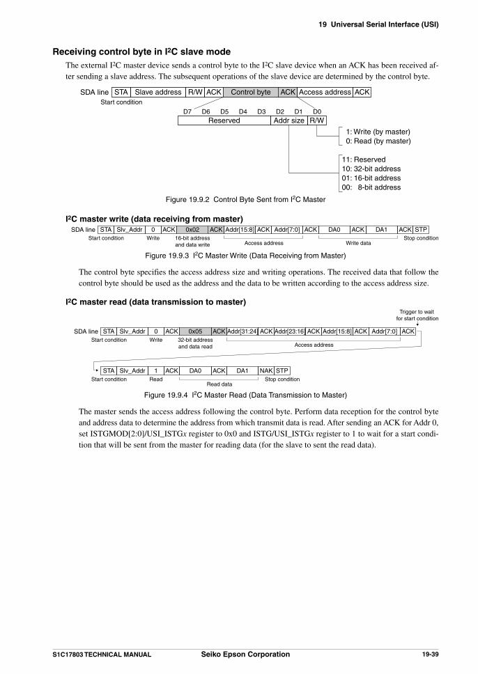
19 Universal Serial Interface (USI)
S1C17803 TECHNICAL MANUAL Seiko Epson Corporation 19-39
Receiving control byte in I2C slave mode The external I2C master device sends a control byte to the I2C slave device when an ACK has been received af-
ter sending a slave address. The subsequent operations of the slave device are determined by the control byte.
SDA line
1: Write (by master) 0: Read (by master)
11: Reserved10: 32-bit address01: 16-bit address00: 8-bit address
Start condition
D7 D6 D5 D4 D3 D2 D1 D0
STA
Reserved Addr size R/W
ACKR/W ACK ACKSlave address Access addressControl byte
Figure 19.9.2 Control Byte Sent from I2C Master
I2C master write (data receiving from master)SDA line
Start condition Write 16-bit addressand data write
STAStop condition
Access address
STPACK ACK ACKSlv_Addr Addr[15:8] ACKAddr[7:0] ACKDA0 ACKDA10x02
Write data
0
Figure 19.9.3 I2C Master Write (Data Receiving from Master)
The control byte specifies the access address size and writing operations. The received data that follow the control byte should be used as the address and the data to be written according to the access address size.
I2C master read (data transmission to master)
SDA lineStart condition
STA
Stop condition
Trigger to wait for start condition
STP
ACK0Write 32-bit address
and data read
ACK ACKSlv_Addr
Start condition
STA ACK1Read
Slv_Addr
Addr[31:24] ACKAddr[23:16] ACKAddr[15:8] ACKAddr[7:0]
ACKDA0 NAKDA1
0x05
Access address
Read data
Figure 19.9.4 I2C Master Read (Data Transmission to Master)
The master sends the access address following the control byte. Perform data reception for the control byte and address data to determine the address from which transmit data is read. After sending an ACK for Addr 0, set ISTGMOD[2:0]/USI_ISTGx register to 0x0 and ISTG/USI_ISTGx register to 1 to wait for a start condi-tion that will be sent from the master for reading data (for the slave to sent the read data).

20 I2C Master (I2CM)
S1C17803 TECHNICAL MANUAL Seiko Epson Corporation 20-1
20 I2C Master (I2CM)
20.1 I2CM Module OverviewThe S1C17803 incorporates an I2C master (I2CM) module for high-speed synchronized serial communications.The following shows the main features of I2CM:
• Operates as an I2C bus master device (as single master only).
• Supports standard (100 kbps) and fast (400 kbps) modes.
• 7-bit addressing mode (10-bit addressing is possible by software control.)
• Includes one-byte receive data buffer and one-byte transmit buffer.
• Includes a noise filter function to help improve the reliability of data transfers.
• Can generate transmit buffer empty and receive buffer full interrupts.
Figure 20.1.1 shows the I2CM configuration.
Shift register I2CM_SDA
SD
A
SC
L
I2CM_SCL
I2CM_CLK(from CLG_T8I)
Internal bus
ITC
I2C master
Bus I/Fand
controlregisters
Shift register
Clock/transfer control
Noisefilter
Interruptcontrol
Figure 20.1.1 I2CM Configuration
20.2 I2CM Input/Output PinsTable 20.2.1 lists the I2CM pins.
Table 20.2.1 List of I2CM Pins
Pin name I/O Qty FunctionI2CM_SDA I/O 1 I2CM data input/output pin
Inputs serial data from the I2C bus. Also outputs serial data to the I2C bus. I2CM_SCL I/O 1 I2CM SCL input/output pin
Inputs SCL line status. Also outputs a serial clock.
The I2CM input/output pins (I2CM_SDA, I2CM_SCL) are shared with I/O ports and are initially set as general purpose I/O port pins. The pin functions must be switched using the port function select bits to use the general pur-pose I/O port pins as I2CM input/output pins.For detailed information on pin function switching, see the “I/O Ports (GPIO)” chapter.
20.3 I2C Master ClockThe I2CM module uses the I2CM_CLK clock output by CLG_T8I as the synchronization clock. This clock is output from the I2CM_SCL pin to the slave device while also driving the shift register. The clock should be pro-grammed to output a signal matching the transfer rate from CLG_T8I. For more information on CLG_T8I control, see the “Clock Generator (CLG)” chapter.

20 I2C Master (I2CM)
20-2 Seiko Epson Corporation S1C17803 TECHNICAL MANUAL
If the I2C master module communicates with a slave device which has clock stretching, Transfer rates are limited up to 50 kbits/s in the Standard-mode, up to 200 kbits in the Fast-mode.
The I2CM module does not function as a slave device. The I2CM_SCL input pin is used to check the I2C bus SCL signal status. It is not used for synchronization clock input.
20.4 Settings Before Data TransferThe I2CM module includes an optional noise filter function that can be selected via the application program.
Noise filter function The I2CM module incorporates a function for filtering noise from the I2CM_SDA and I2CM_SCL pin input
signals. This function is enabled by setting NSERM/I2CM_CTL register to 1. Note that using this function requires setting the I2CM clock (CLG_T8I output clock) frequency to 1/6 or less
of PCLK_SOC.
20.5 Data Transfer ControlMake the following settings before starting data transfers. (1) Configure CLG_T8I to output the I2CM_CLK clock. (See the CLG chapter.) (2) Select the option function. (See Section 20.4.) (3) Set the interrupt conditions to use I2CM interrupts. (See Section 20.6.)
Note: Make sure the I2CM module is halted (I2CMEN/I2CM_EN register = 0) before changing the above settings.
Enabling data transfers Set I2CMEN/I2CM_EN register to 1 to enable I2CM operations. This enables I2CM transfers and clock input/
output.
Note: Do not set I2CMEN to 0 when the I2CM module is transferring data.
Starting Data transfer To start data transfers, the I2C master (this module) must generate a start condition. The slave address is then
sent to establish communications.
(1) Generating start condition The start condition applies when the SCL line is maintained at high and the SDA line is pulled down to low.
I2CM_SDA (output)
I2CM_SCL (output)
Start condition
Figure 20.5.1 Start Condition
The start condition is generated by setting STRT/I2CM_CTL register to 1. STRT is automatically reset to 0 once the start condition is generated. The I2C bus is busy from this point on.
(2) Slave address transmission Once the start condition has been generated, the I2C master (this module) sends a bit indicating the slave address
and transfer direction for communications. I2C slave addresses are either 7-bit or 10-bit. This module uses an 8-bit transfer data register to send the slave address and transfer direction bit, enabling single transfers in 7-bit address mode. In 10-bit mode, data is sent twice under software control. Figure 20.5.2 shows the configuration of the address data.

20 I2C Master (I2CM)
S1C17803 TECHNICAL MANUAL Seiko Epson Corporation 20-3
Slave address
7-bit address
Transfer direction0: Master slave (data transmission)1: Slave master (date reception)
A6 A5 D7 D6
A4 D5
A3 D4
A2 D3
A1 D2
A0 D1
DIR D0
Slave address last 8 bits
A7 A6 D7 D6
A5 D5
A4 D4
A3 D3
A2 D2
A1 D1
A0 D0
Slave addressfirst 2 bits
10-bit address
1 First data sent
Second data sent
1 D7 D6
1 D5
1 D4
0 D3
A9 D2
A8 D1
0D0
Data reception
After Second data sent, generate repeated START condition and send third data
Slave addressfirst 2 bits
1Third data sent 1D7 D6
1D5
1D4
0D3
A9D2
A8D1
1D0
Figure 20.5.2 Transmit Data Specifying Slave Address and Transfer Direction
The transfer direction bit indicates the data transfer direction after the slave address has been sent. This is set to 0 when sending data from the master to the slave and to 1 when receiving data from the slave. To send a slave address, set the address with the transfer direction bit to RTDT[7:0]/I2CM_DAT register. At the same time, set TXE/I2CM_DAT register transmitting the address to 1.
After the slave address has been output, data can be sent and received as many times as required. Data must be sent or received according to the transfer direction set together with the slave address.
Data transmission control The procedure for transmitting data is described below. Data transmission is performed by the same procedure
as for slave address transmission. To send byte data, set the transmit data to RTDT[7:0] and set TXE to 1 to transmit 1 byte. When TXE is set to 1, the I2CM module begins data transmission in sync with the clock. If the previous data
is currently being transmitted, data transmission starts after this has been completed. The I2CM module first transfers the data written to the shift register, then starts outputting the clock from the I2CM_SCL pin. TXE is reset to 0 at this point and a cause of interrupt occurs, enabling the subsequent transmission data and TXE to be set.
The data bits in the shift register are shifted in sequence at the clock falling edge and output via the I2CM_SDA pin with the MSB leading. The I2CM module outputs 9 clocks with each data transmission. In the 9th clock cycle, the I2CM module sets the SDA line into high impedance to receive an ACK or NAK sent from the slave device.
The slave device returns ACK (0) to the master if the data is received. If the data is not received, the SDA line is not pulled down, which the I2CM module interprets to mean a NAK (1) (transmission failed).
I2CM_SDA (output)
I2CM_SDA (input)
I2CM_SCL (output)
Start condition
1 2 8 9
D7 D6 D0
ACK
NAK
Figure 20.5.3 ACK and NAK

20 I2C Master (I2CM)
20-4 Seiko Epson Corporation S1C17803 TECHNICAL MANUAL
The I2CM module includes two status bits for transmission control: TBUSY/I2CM_CTL register and RTACK/I2CM_DAT register.
The TBUSY flag indicates the data transmission status. This flag becomes 1 when transmission starts (including slave address transmission) and reverts to 0 once data transmission ends. Inspect the flag to check whether the I2CM module is currently transmitting or at standby.
The RTACK bit indicates whether or not the slave device returned an ACK for the previous transmission. RT-ACK is 0 if an ACK was returned and 1 if ACK was not returned.
Data reception control The procedure for receiving data is described below. When receiving data, the slave address must be sent with
the transfer direction bit set to 1. To receive data, set RXE/I2CM_DAT register to 1 for receiving 1 byte. When TXE/I2CM_DAT register is set
to 1 for sending the slave address, RXE can also be set to 1 at the same time. If both TXE and RXE are set to 1, TXE takes priority.
When RXE is set to 1, allowing receiving to start, the I2CM module starts outputting the clock from the I2CM_SCL pin with the SDA line at high impedance. The data is shifted into the shift register with the clock pulses, with the MSB leading.
RXE is reset to 0 when D7 is loaded. The received data is loaded to RTDT[7:0] once the 8-bit data has been received in the shift register.
The I2CM module includes two status bits for receive control: RBRDY/I2CM_DAT register and RBUSY/ I2CM_CTL register.
The RBRDY flag indicates the received data status. This flag becomes 1 when the data received in the shift regis-ter is loaded to RTDT[7:0] and reverts to 0 when the received data is read out from RTDT[7:0]. Interrupts can also be generated once the flag value becomes 1.
The RBUSY flag indicates the receiving operation status. This flag is 1 when receiving starts and reverts to 0 when the data is received. Inspect the flag to determine whether the I2CM module is currently receiving or in standby.
To wait for reception using polling, follow the procedures given below using the RBUSY flag. Interrupts to the CPU are disabled because polling accurately determines the two state transitions 3 and 4.
1. Disable interrupts to the CPU using the di instruction. 2. Write 1 to RXE to prepare for receiving. 3. Wait for RBUSY to become 1 (reception start). 4. Wait for RBUSY to become 0 (reception end). 5. Read out RTDT (received data). 6. Enables interrupts to the CPU using the ei instruction.
The I2CM module outputs 9 clocks with each data reception. In the 9th clock cycle, an ACK or NAK is sent to the slave via the I2CM_SDA pin. The bit state sent can be set in RTACK/I2CM_DAT register. To send ACK, set RTACK to 0. To send NAK, set RTACK to 1.
End of data transfers (Generating stop condition) To end data transfers after all data has been transferred, the I2C master (this module) must generate a stop con-
dition. The stop condition applies when the SCL line is maintained at high and the SDA line is pulled up from low to high.
I2CM_SDA (output)
I2CM_SCL (output)
Stop condition
Figure 20.5.4 Stop Condition
The stop condition is generated by setting STP/I2CM_CTL register to 1. When STP is set to 1, the I2CM module pulls up the I2C bus SDA line from low to high with the SCL line
maintained at high to generates a stop condition. The I2C bus subsequently switches to free state. When transmission or reception ends, TBUSY or RBUSY is cleared. Then, after a period longer than the 1/4
cycle of I2C clock, STP can set to 1. Also, to generate stop condition to the slave device which has clock stretch function, please write 1 to STP after data transfer (including ACK/NAK transfer) and a period until the slave device stops clock stretch.

20 I2C Master (I2CM)
S1C17803 TECHNICAL MANUAL Seiko Epson Corporation 20-5
Continuing data transfer (Generating Repeated start condition) To make it possible to continue with a different data transfer after data transfer completion, the I2C master (this
module) can generate a repeated start condition.
I2CM_SDA (output)
I2CM_SCL (output)
Repeated start condition
Figure 20.5.5 Repeated Start Condition
The repeated start condition is generated by setting STRT/I2CM_CTL register to 1 when the I2C bus is busy. STRT is automatically reset to 0 once the repeated start condition is generated. Slave address transmission is
subsequently possible with the I2C bus remaining in the busy state.
Disabling data transfer After STOP condition generation, write 0 to I2CMEN to disable data transfers. For this case, the STP may be
polled to determine the end of STOP condition generation when it is cleared. If I2CEN is set to 0 when I2C bus is busy, SCL0, SDA0 output level nor no information is guaranteed.
Timing chart
PCLK_SOC
CLG_T8I output
I2CM_SCL
I2CM_SDA
STRT
STRT settingStart condition I2C bus busy
Figure 20.5.6 Start Condition Generation
PCLK_SOC
CLG_T8I output
I2CM_SCL
I2CM_SDA
TXE
TBUSY
RTACK
RTDT[7:0]
Interrupt
D[7:0] D[7:0]
A6/D7 A5/D6 DIR/D0 ACK
TXE setting Transmit data setting ACK receivingTransmission end
Transmission start
Figure 20.5.7 Slave Address Transmission/Data Transmission
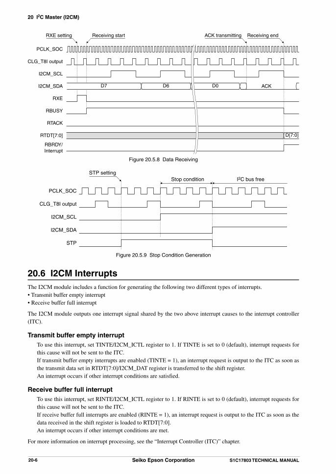
20 I2C Master (I2CM)
20-6 Seiko Epson Corporation S1C17803 TECHNICAL MANUAL
PCLK_SOC
CLG_T8I output
I2CM_SCL
I2CM_SDA
RXE
RBUSY
RTACK
RTDT[7:0]
RBRDY/Interrupt
D[7:0]
D7 D6 D0 ACK
RXE setting ACK transmitting Receiving endReceiving start
Figure 20.5.8 Data Receiving
PCLK_SOC
CLG_T8I output
I2CM_SCL
I2CM_SDA
STP
STP settingStop condition I2C bus free
Figure 20.5.9 Stop Condition Generation
20.6 I2CM InterruptsThe I2CM module includes a function for generating the following two different types of interrupts. • Transmit buffer empty interrupt • Receive buffer full interrupt
The I2CM module outputs one interrupt signal shared by the two above interrupt causes to the interrupt controller (ITC).
Transmit buffer empty interrupt To use this interrupt, set TINTE/I2CM_ICTL register to 1. If TINTE is set to 0 (default), interrupt requests for
this cause will not be sent to the ITC. If transmit buffer empty interrupts are enabled (TINTE = 1), an interrupt request is output to the ITC as soon as
the transmit data set in RTDT[7:0]/I2CM_DAT register is transferred to the shift register. An interrupt occurs if other interrupt conditions are satisfied.
Receive buffer full interrupt To use this interrupt, set RINTE/I2CM_ICTL register to 1. If RINTE is set to 0 (default), interrupt requests for
this cause will not be sent to the ITC. If receive buffer full interrupts are enabled (RINTE = 1), an interrupt request is output to the ITC as soon as the
data received in the shift register is loaded to RTDT[7:0]. An interrupt occurs if other interrupt conditions are met.
For more information on interrupt processing, see the “Interrupt Controller (ITC)” chapter.

20 I2C Master (I2CM)
S1C17803 TECHNICAL MANUAL Seiko Epson Corporation 20-7
20.7 Control Register Details
Table 20.7.1 List of I2CM RegistersAddress Register name Function
0x4340 I2CM_EN I2C Master Enable Register Enables the I2C master module.0x4342 I2CM_CTL I2C Master Control Register Controls the I2C master operation and indicates transfer status.0x4344 I2CM_DAT I2C Master Data Register Transmit/receive data
0x4346 I2CM_ICTL I2C Master Interrupt Control Register Controls the I2C master interrupt.
The I2CM module registers are described in detail below. These are 16-bit registers.
Note: When data is written to the registers, the “Reserved” bits must always be written as 0 and not 1.
I2C Master Enable Register (I2CM_EN)Register name Address Bit Name Function Setting Init. R/W Remarks
I2C Master Enable Register(I2CM_EN)
0x4340(16 bits)
D15–1 – reserved – – – 0 when being read.
D0 I2CMEN I2C master enable 1 Enable 0 Disable 0 R/W
D[15:1] Reserved
D0 I2CMEN: I2C Master Enable Bit Enables or disables I2CM module operation. 1 (R/W): Enabled 0 (R/W): Disabled (default) Setting I2CMEN to 1 starts the I2CM module operation, enabling data transfer. Setting I2CMEN to 0
stops the I2CM module operation.
I2C Master Control Register (I2CM_CTL)Register name Address Bit Name Function Setting Init. R/W Remarks
I2C Master Control Register(I2CM_CTL)
0x4342(16 bits)
D15–10 – reserved – – – 0 when being read.D9 RBUSY Receive busy flag 1 Busy 0 Idle 0 RD8 TBUSY Transmit busy flag 1 Busy 0 Idle 0 R
D7–5 – reserved – – – 0 when being read.D4 NSERM Noise remove on/off 1 On 0 Off 0 R/W
D3–2 – reserved – – – 0 when being read.D1 STP Stop control 1 Stop 0 Ignored 0 R/WD0 STRT Start control 1 Start 0 Ignored 0 R/W
D[15:10] Reserved
D9 RBUSY: Receive Busy Flag Bit Indicates the I2CM receiving status. 1 (R): Operating 0 (R): Standby (default)
RBUSY is set to 1 when the I2CM starts data receiving and is maintained at 1 while receiving is under-way. It is cleared to 0 once reception is completed.
D8 TBUSY: Transmit Busy Flag Bit Indicates the I2CM transmission status. 1 (R): Operating 0 (R): Standby (default)
TBUSY is set to 1 when the I2CM starts data transmission and is maintained at 1 while transmission is underway. It is cleared to 0 once transmission is completed.
D[7:5] Reserved

20 I2C Master (I2CM)
20-8 Seiko Epson Corporation S1C17803 TECHNICAL MANUAL
D4 NSERM: Noise Remove On/Off Bit Turns the noise filter function on or off. 1 (R/W): On 0 (R/W): Off (default)
The I2CM module incorporates a function for filtering noise from the I2CM_SDA and I2CM_SCL pin input signals. This function is enabled by setting NSERM to 1. Note that using this function requires setting the I2CM_CLK clock (CLG_T8I output clock) frequency to 1/6 or less of PCLK_SOC.
D[3:2] Reserved
D1 STP: Stop Control Bit Generates the stop condition. 1 (R/W): Stop condition generated 0 (R/W): Ineffective (default)
By setting STP to 1, the I2CM module generates the stop condition by pulling up the I2C bus SDA line from low to high with the SCL line maintaining at high. The I2C bus subsequently becomes free. Note that the stop condition will be generated only if STP is 1 and TXE/I2CM_DAT register, RXE/I2CM_DAT register, and STRT are set to 0 when data transfer is completed (including ACK transfer). STP is automatically reset to 0 if the stop condition is generated.
D0 STRT: Start Control Bit Generates the start condition. 1 (R/W): Start condition generated 0 (R/W): Ineffective (default)
By setting STRT to 1, the I2CM module generates the start condition by pulling down the I2C bus SDA line to low with SCL line maintaining at high.
The repeated start condition can be generated by setting STRT to 1 when the I2C bus is busy. STRT is automatically reset to 0 once the start condition or repeated start condition is generated. The
I2C bus subsequently becomes busy.
I2C Master Data Register (I2CM_DAT)Register name Address Bit Name Function Setting Init. R/W Remarks
I2C Master Data Register(I2CM_DAT)
0x4344(16 bits)
D15–12 – reserved – – – 0 when being read.D11 RBRDY Receive buffer ready flag 1 Ready 0 Empty 0 RD10 RXE Receive execution 1 Receive 0 Ignored 0 R/WD9 TXE Transmit execution 1 Transmit 0 Ignored 0 R/WD8 RTACK Receive/transmit ACK 1 Error 0 ACK 0 R/W
D7–0 RTDT[7:0] Receive/transmit dataRTDT7 = MSBRTDT0 = LSB
0x0 to 0xff 0x0 R/W
D[15:12] Reserved
D11 RBRDY: Receive Buffer Ready Flag Bit Indicates the receive buffer status. 1 (R): Receive data exists 0 (R): No receive data (default)
The RBRDY flag becomes 1 when the data received in the shift register is loaded to RTDT[7:0] and reverts to 0 when the receive data is read out from RTDT[7:0]. Interrupts can also be generated once the flag value becomes 1.
Note: Use the RBUSY flag when awaiting reception using polling. The RBRDY flag cannot be used to await reception with polling. For more information on awaiting reception control procedures using polling, refer to “Data reception control” in Section 20.5.

20 I2C Master (I2CM)
S1C17803 TECHNICAL MANUAL Seiko Epson Corporation 20-9
D10 RXE: Receive Execution Bit Receives 1 byte of data. 1 (R/W): Data reception start 0 (R/W): Ineffective (default) Setting RXE to 1 and TXE to 0 starts receiving for 1 byte of data. RXE can be set to 1 for subsequent re-
ception, even if the slave address is being sent or data is being received. RXE is reset to 0 as soon as D6 is loaded to the shift register.
D9 TXE: Transmit Execution Bit Transmits 1 byte of data. 1 (R/W): Data transmission start 0 (R/W): Ineffective (default)
Transmission is started by setting the transmit data to RTDT[7:0] and writing 1 to TXE. TXE can be set to 1 for subsequent transmission, even if the slave address or data is being sent. TXE is reset to 0 as soon as the data set in RTDT[7:0] is transferred to the shift register.
D8 RTACK: Receive/Transmit ACK Bit
When transmitting data Indicates the response bit status. 1 (R/W): Error (NAK) 0 (R/W): ACK (default)
RTACK becomes 0 when ACK is returned from the slave after 1 byte of data is sent, indicating that the slave has received the data correctly. If RTACK is 1, the slave device is not operating or the data was not received correctly.
When receiving data Sets the response bit sent to the slave. 1 (R/W): Error (NAK) 0 (R/W): ACK (default)
To return an ACK after data has been received, RTACK should be set to 0 before the I2CM module sends the response bit. To return a NAK, set RTACK to 1.
D[7:0] RTDT[7:0]: Receive/Transmit Data Bits
When transmitting data Sets the transmit data. (Default: 0x0) Data transmission is started by setting TXE to 1. If a slave address or data is currently being transmit-
ted, transmission begins once the previous transmission is completed. Serial converted data is output from the I2CM_SDA pin with MSB leading and bits set to 0 as low level. A cause of transmit buffer empty interrupt is generated as soon as the data written to this register is transferred to the shift regis-ter, after which the subsequent transmission data can be written.
When receiving data The received data can be read out. (Default: 0x0) Data reception is started by setting RXE to 1. If a slave address is currently being transmitted or data
is currently being received, the new reception starts once the previous data has been transferred. The RBRDY flag is set and a cause of receive buffer full interrupt generated as soon as reception is com-pleted and the shift register data is transferred to this register. Data can then be read until the subsequent data has been received. If the subsequent data is received before this register is read out, the contents are overwritten by the most recent received data. Serial data input from the I2CM_SDA pin with MSB leading is converted to parallel, with the high level bit set to 1 and the low level bit set to 0, then loaded to this register.

20 I2C Master (I2CM)
20-10 Seiko Epson Corporation S1C17803 TECHNICAL MANUAL
I2C Master Interrupt Control Register (I2CM_ICTL)Register name Address Bit Name Function Setting Init. R/W Remarks
I2C Master Interrupt Control Register(I2CM_ICTL)
0x4346(16 bits)
D15–2 – reserved – – – 0 when being read.D1 RINTE Receive interrupt enable 1 Enable 0 Disable 0 R/WD0 TINTE Transmit interrupt enable 1 Enable 0 Disable 0 R/W
D[15:2] Reserved
D1 RINTE: Receive Interrupt Enable Bit Enables or disables I2CM receive buffer full interrupts. 1 (R/W): Enabled 0 (R/W): Disabled (default)
Setting RINTE to 1 enables the output of I2CM interrupt requests to the ITC due to a receive data buf-fer full. These interrupt requests are generated when the data received in the shift register is transferred to RTDT[7:0]/I2CM_DAT register (when reception is completed).
I2CM interrupts are not generated by receive data buffer full if RINTE is set to 0.
D0 TINTE: Transmit Interrupt Enable Bit Enables or disables I2CM transmit buffer empty interrupts. 1 (R/W): Enabled 0 (R/W): Disabled (default)
Setting TINTE to 1 enables the output of I2CM interrupt requests to the ITC due to a transmit buffer empty. These interrupt requests are generated when the data written to RTDT[7:0] is transferred to the shift register.
I2CM interrupts are not generated by transmit buffer empty if TINTE is set to 0.
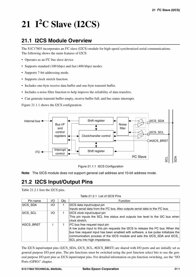
21 I2C Slave (I2CS)
S1C17803 TECHNICAL MANUAL Seiko Epson Corporation 21-1
21 I2C Slave (I2CS)
21.1 I2CS Module OverviewThe S1C17803 incorporates an I2C slave (I2CS) module for high-speed synchronized serial communications. The following shows the main features of I2CS:
• Operates as an I2C bus slave device.
• Supports standard (100 kbps) and fast (400 kbps) modes.
• Supports 7-bit addressing mode.
• Supports clock stretch function.
• Includes one-byte receive data buffer and one-byte transmit buffer.
• Includes a noise filter function to help improve the reliability of data transfers.
• Can generate transmit buffer empty, receive buffer full, and bus status interrupts.
Figure 21.1.1 shows the I2CS configuration.
Shift register
SD
A
SC
L
Internal bus
ITC
I2C Slave
Bus I/Fand
controlregisters
Shift register
Clock/transfer control
Interruptcontrol
#I2CS_BRST
I2CS_SDA
I2CS_SCL
Noisefilter
Figure 21.1.1 I2CS Configuration
Note: The I2CS module does not support general call address and 10-bit address mode.
21.2 I2CS Input/Output PinsTable 21.2.1 lists the I2CS pins.
Table 21.2.1 List of I2CS Pins
Pin name I/O Qty FunctionI2CS_SDA I/O 1 I2CS data input/output pin
Inputs serial data from the I2C bus. Also outputs serial data to the I2C bus. I2CS_SCL I/O 1 I2CS clock input/output pin
This pin inputs the SCL line status and outputs low level to the I2C bus when clock stretch.
#I2CS_BRST I 1 I2C bus free request input pinA low pulse input to this pin requests the I2CS to release the I2C bus. When the bus free request input has been enabled with software, a low pulse initializes the communication process of the I2CS module and sets the I2CS_SDA and I2CS_SCL pins into high impedance.
The I2CS input/output pins (I2CS_SDA, I2CS_SCL, #I2CS_BRST) are shared with I/O ports and are initially set as general purpose I/O port pins. The pin functions must be switched using the port function select bits to use the gen-eral purpose I/O port pins as I2CS input/output pins. For detailed information on pin function switching, see the “I/O Ports (GPIO)” chapter.

21 I2C Slave (I2CS)
21-2 Seiko Epson Corporation S1C17803 TECHNICAL MANUAL
21.3 I2C Slave ClockThe I2CS module operates with the clock output from the external I2C master device by inputting it from the I2CS_SCL pin. The I2CS module also uses the system clock (PCLK_SOC) for its operations. The PCLK_SOC frequency must be set eight-times or higher than the I2CS_SCL input clock frequency during data transfer. In standby status, use of the asynchronous address detection function allows the application to lower the PCLK_SOC clock frequency to re-duce current consumption. For more information, see “Asynchronous address detection function” in Section 21.4.3.
21.4 Initializing I2CS
21.4.1 Reset
The I2CS module must be reset to initialize the communication process and to set the I2C bus into free status (high impedance). The following shows two methods for resetting the module:
(1) Software reset The I2CS module can be reset using SOFTRESET/I2CS_CTL register. To reset the I2CS module, write 1 to SOFTRESET to place the I2CS module into reset status, then write 0 to SOFTRE-
SET to release it from reset status. It is not necessary to insert a waiting time between writing 1 and 0. The I2CS module initializes the I2C communication process and put the I2CS_SDA and I2CS_SCL pins into high-im-
pedance to be ready to detect a start condition. Furthermore, the I2CS control bits except for SOFTRESET are initialized. Perform the software reset in the initial setting process before staring communication.
(2) Bus free request with an input from the #I2CS_BRST pin The I2CS module can accept bus free requests via the #I2CS_BRST pin. The bus free request support is dis-
abled by default. To enable this function, set BFREQ_EN/I2CS_CTL register to 1. When this function is enabled, a low pulse (one system clock (PCLK) cycle is required. Two PCLK cycles or
more pulse width is recommended) input to the #I2CS_BRST pin sets BFREQ/I2CS_STAT register to 1. This initializes the I2C communication process and puts the I2CS_SDA and I2CS_SCL pins into high-impedance. The control registers will not be initialized as distinct from the software reset described above.
Note: When BFREQ is set to 1 (an interrupt can be used for checking this status), perform a software reset and set the registers again.
21.4.2 Setting Slave Address
I2C devices have a unique slave address to identify each device.The I2CS module supports 7-bit address (does not support 10-bit address), and the address of this module must be set to SADRS[6:0]/I2CS_SADRS register.
21.4.3 Optional Functions
The I2CS module has a clock stretch, asynchronous address detection, and noise filter optional functions selectable in the application program.
Clock stretch function After data and ACK are transmitted or received, the slave device may issue a wait request to the master device
until it is ready to transmit/receive by pulling the I2C bus SCL line down to low. The I2CS module supports this clock stretch function. The master device enters a standby state until the wait request is canceled (the SCL line goes high). The clock stretch function in this module is disabled by default. When using the clock stretch func-tion, set CLKSTR_EN/I2CS_CTL register to 1 before starting data communication.
Note: When I2C slave module is slave transceiver mode, the data setup time with clock stretching (= the period from outputting the MSB of SDATA[7:0] on SDA1 pin to ending SCL1 Low hold) depends on the PCLK frequency.

21 I2C Slave (I2CS)
S1C17803 TECHNICAL MANUAL Seiko Epson Corporation 21-3
Asynchronous address detection function The I2CS module operation clock (PCLK_SOC) frequency must be set eight-times or higher than the transfer
rate during data transfer. However, the PCLK_SOC frequency can be lowered to reduce current consumption if no other processing is required during standby for data transfer. The asynchronous address detection function is provided to detect the I2C slave address sent from the master in this status.
The asynchronous address detection function in this module is disabled by default. When using the asynchro-nous address detection function, set ASDET_EN/I2CS_CTL register to 1.
If the slave address sent from the master has matched with one that has been set in this I2CS module when the asynchronous address detection function has been enabled, the I2CS module generates a bus status interrupt and returns NAK to the I2C master to request for resending the slave address.
Set the PCLK_SOC frequency to eight-times or higher than the transfer rate and reset ASDET_EN to 0 in the interrupt handler routine. Data transfer will be able to resume normally after the master retries transmission. Af-ter the master generates a stop condition to put the I2C bus into free status, the asynchronous address detection function can be enabled again to lower the operating speed.
Notes: • When the asynchronous address detection function is enabled, the I2C bus signals are input without passing through the noise filter. Therefore, the slave address may not be detected in a high-noise environment.
• When the asynchronous address detection function is enabled, data transfer cannot be per-formed even if the PCLK_SOC frequency is eight-times or higher than the transfer rate. Be sure to disable the asynchronous address detection function during normal operation.
Noise filter The I2CS module includes a function to remove noise from the I2CS_SDA and I2CS_SCL input signals. This
function is enabled by setting NF_EN/I2CS_CTL register to 1.
21.5 Data Transfer ControlMake the following settings before starting data transfers. (1) Initialize the I2CS module. See Section 21.4.(2) Set the interrupt conditions to use I2CS interrupt. See Section 21.6.
Note: Make sure that the I2CS module is disabled (I2CSEN/I2CS_CTL register = 0) before setting the conditions above.
Enabling data transfers First, set I2CSEN/I2CS_CTL register to 1 to enable I2CS operation. This makes the I2CS in ready-to-transmit/
receive status in which a start condition can be detected.
Note: Do not set the I2CSEN bit to 0 while the I2CS module is transmitting/receiving data.
Starting data transfer To start data transmission/reception, set COM_MODE/I2CS_CTL register to 1 to enable data communications. When the slave address for this module that has been sent from the master is received after a start condition is
detected, the I2CS module returns an ACK (I2CS_SDA = low) and starts operating for data reception or data transmission according to the transfer direction bit that has been received with the slave address.
When COM_MODE is 0 (default), the I2CS module does not send back a response if the master has sent the slave address of this module (it is regarded as that the I2CS module has returned a NAK to the master).

21 I2C Slave (I2CS)
21-4 Seiko Epson Corporation S1C17803 TECHNICAL MANUAL
I2CS_SDA (input)
I2CS_SDA (output)
I2CS_SCL (input)
Start condition
1 2 3 4 5 6 7 8 9
ACK
NAK
7-bit slave address
Transfer direction0: master → slave (data reception)1: slave → master (data transmission)
A6 A5D7 D6
A4D5
A3D4
A2D3
A1D2
A0D1
R/WD0
Figure 21.5.1 Receiving Slave Address and Data Direction Bit
When a start condition is detected, BUSY/I2CS_ASTAT register is set to 1 to indicate that the I2C bus is put into busy status. When the slave address of this module is received, SELECTED/I2CS_ASTAT register is set to 1 to indicate that this module has been selected as the I2C slave device. STOP condition detection clears BUSY. STOP or Repeated START condition detection clears SELECTED.
The value of the transfer direction bit is set to R/W/I2CS_ASTAT register, so use R/W to select the transmit- or receive-handling.
If the slave address of this module is detected when the asynchronous address detection function has been en-abled, ASDET/I2CS_STAT register is set to 1. The I2CS module generates a bus status interrupt and returns NAK to the I2C master to request for resending the slave address. Set the PCLK_SOC frequency to eight-times or higher than the transfer rate and disable the asynchronous address detection function in the interrupt handler routine. Data transfer will be able to resume normally after the master retries transmission. ASDET can be cleared by writing 1.
Data transmission The following describes a data transmission procedure. The I2CS module starts data transmission process when both SELECTED and R/W are set to 1. It sets TXEMP/
I2CS_ASTAT register to 1 to issue a request to the application program to write transmit data. Write transmit data to SDATA[7:0]/I2CS_TRNS register.
When setting the first transmit data after this module has been selected as the slave device, follow the precau-tions described below.
When the clock stretch function is disabled (default) Transmit data must be written to SDATA[7:0] within 1 cycle of the I2C clock (I2CS_SCL input clock) after
TXEMP has been set to 1. This time is not enough for data preparation, so write transmit data before TX-EMP has been set to 1. If the previous transmit data is still stored in SDATA[7:0], it is overwritten with the new data to be transferred. Therefore, the clear operation (see below) using TBUF_CLR is unnecessary.
When the clock stretch function is enabled The master device is placed into wait status by the clock stretch function, so transmit data can be written
after TXEMP is set. However, if the previous transmit data is still stored in SDATA[7:0], it will be sent im-mediately after TXEMP has been set. In order to avoid this problem, clear the I2CS_TRNS register using TBUF_CLR/I2CS_CTL register before this module is selected as the slave device. The I2CS_TRNS regis-ter is cleared by writing 1 to TBUF_CLR then writing 0 to it.
It is not necessary to clear the I2CS_TRNS register if the first transmit data is written before TXEMP has been set.
For writing transmit data other than the first time, use an interrupt that can be generated when TXEMP is set to 1. TXEMP is also set to 1 when the transmit data written to SDATA[7:0] is loaded to the sift register during transmission. TXEMP is cleared by writing transmit data to SDATA[7:0].
When the clock stretch function is disabled (default) When the clock stretch function has been disabled, data must be written to the I2CS_TRNS register within
7 cycles of the I2C clock (I2CS_SCL input clock) from TXEMP being set to 1. If data has not been written in this period, the current register value (previous transmit data) will be sent.
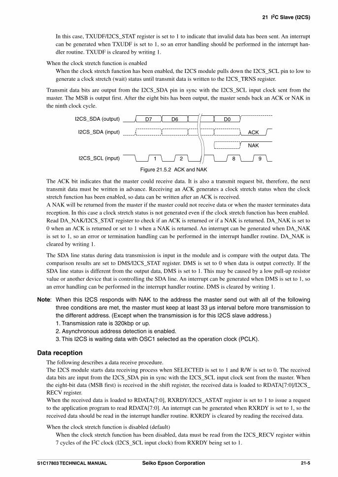
21 I2C Slave (I2CS)
S1C17803 TECHNICAL MANUAL Seiko Epson Corporation 21-5
In this case, TXUDF/I2CS_STAT register is set to 1 to indicate that invalid data has been sent. An interrupt can be generated when TXUDF is set to 1, so an error handling should be performed in the interrupt han-dler routine. TXUDF is cleared by writing 1.
When the clock stretch function is enabled When the clock stretch function has been enabled, the I2CS module pulls down the I2CS_SCL pin to low to
generate a clock stretch (wait) status until transmit data is written to the I2CS_TRNS register.
Transmit data bits are output from the I2CS_SDA pin in sync with the I2CS_SCL input clock sent from the master. The MSB is output first. After the eight bits has been output, the master sends back an ACK or NAK in the ninth clock cycle.
I2CS_SDA (output)
I2CS_SDA (input)
I2CS_SCL (input) 1 2 8 9
D7 D6 D0
ACK
NAK
Figure 21.5.2 ACK and NAK
The ACK bit indicates that the master could receive data. It is also a transmit request bit, therefore, the next transmit data must be written in advance. Receiving an ACK generates a clock stretch status when the clock stretch function has been enabled, so data can be written after an ACK is received.
A NAK will be returned from the master if the master could not receive data or when the master terminates data reception. In this case a clock stretch status is not generated even if the clock stretch function has been enabled.
Read DA_NAK/I2CS_STAT register to check if an ACK is returned or if a NAK is returned. DA_NAK is set to 0 when an ACK is returned or set to 1 when a NAK is returned. An interrupt can be generated when DA_NAK is set to 1, so an error or termination handling can be performed in the interrupt handler routine. DA_NAK is cleared by writing 1.
The SDA line status during data transmission is input in the module and is compare with the output data. The comparison results are set to DMS/I2CS_STAT register. DMS is set to 0 when data is output correctly. If the SDA line status is different from the output data, DMS is set to 1. This may be caused by a low pull-up resistor value or another device that is controlling the SDA line. An interrupt can be generated when DMS is set to 1, so an error handling can be performed in the interrupt handler routine. DMS is cleared by writing 1.
Note: When this I2CS responds with NAK to the address the master send out with all of the following three conditions are met, the master must keep at least 33 µs interval before more transmission to the different address. (Except when the transmission is for this I2CS slave address.)
1. Transmission rate is 320kbp or up. 2. Asynchronous address detection is enabled. 3. This I2CS is waiting data with OSC1 selected as the operation clock (PCLK).
Data reception The following describes a data receive procedure. The I2CS module starts data receiving process when SELECTED is set to 1 and R/W is set to 0. The received
data bits are input from the I2CS_SDA pin in sync with the I2CS_SCL input clock sent from the master. When the eight-bit data (MSB first) is received in the shift register, the received data is loaded to RDATA[7:0]/I2CS_RECV register.
When the received data is loaded to RDATA[7:0], RXRDY/I2CS_ASTAT register is set to 1 to issue a request to the application program to read RDATA[7:0]. An interrupt can be generated when RXRDY is set to 1, so the received data should be read in the interrupt handler routine. RXRDY is cleared by reading the received data.
When the clock stretch function is disabled (default) When the clock stretch function has been disabled, data must be read from the I2CS_RECV register within
7 cycles of the I2C clock (I2CS_SCL input clock) from RXRDY being set to 1.

21 I2C Slave (I2CS)
21-6 Seiko Epson Corporation S1C17803 TECHNICAL MANUAL
When the clock stretch function is enabled When the clock stretch function has been enabled, the I2CS module pulls down the I2CS_SCL pin to low to
generate a clock stretch (wait) status until the received data is read from the I2CS_RECV register.
If the next data has been received without reading the received data, RDATA[7:0] will be overwritten. In this case, RXOVF/I2CS_STAT register is set to 1 to indicate that the received data has been overwritten. An inter-rupt can be generated when RXOVF is set to 1, so an error handling should be performed in the interrupt han-dler routine. RXOVF is cleared by writing 1.
To return NAK during data reception During data reception (master transmission), the I2CS module sends back an ACK (I2CS_SDA = low) every
time an 8-bit data has been received (by default setting). The response code can be changed to NAK (I2CS_SDA = Hi-Z) by setting NAK_ANS/I2CS_CTL register. An ACK will be sent when NAK_ANS is 0 or a NAK will be sent when NAK_ANS is set to 1.
NAK_ANS should be set within 7 cycles of the I2C clock (I2CS_SCL input clock) after RXRDY has been set to 1 by receiving data just prior to one required for returning NAK.
I2CS_SCL (input)
I2CS_SDA (input)
I2CS_SDA (output)
RXRDY
NAK_ANS
NAK_ANS setting periodReceive interrupt
6 7 8 9 1
D0D2 D1 D7 D6 D5 D4 D3 D2 D0D1
ACK NAK
2 3 4 5 6 7 8 9
Figure 21.5.3 NAK_ANS Setting and NAK Response Timing
End of data transfer (detecting stop condition) Data transfers will be terminated when the master generates a stop condition. The stop condition is a state in
which the SDA line is pulled up from low to high with the SCL line maintained at high.
I2CS_SDA (input)
I2CS_SCL (input)
Stop condition
Figure 21.5.4 Stop Condition
If a stop condition is detected while the I2CS module is selected as the slave device (SELECTED = 1), the I2CS module sets DA_STOP/I2CS_STAT register to 1. At the same time, it sets the I2CS_SDA and I2CS_SCL pins into high-impedance and initializes the I2C communication process to enter standby state that is ready to detect the next start condition. Also SELECTED and BUSY are reset to 0.
An interrupt can be generated when DA_STOP is set to 1, so a communication terminating process should be performed in the interrupt handler routine. DA_STOP is cleared by writing 1.
Disabling data transfer After data transfer has finished, write 0 to the COM_MODE/I2CS_CTL register to disable data transfer. Always make sure that BUSY and SELECTED are 0 before disabling data transfer. To deactivate the I2CS module, set I2CSEN/I2CS_CTL register to 0.

21 I2C Slave (I2CS)
S1C17803 TECHNICAL MANUAL Seiko Epson Corporation 21-7
Timing charts
PCLK_OSC
I2CS_SCL (input)
I2CS_SCL (output)
I2CS_SDA (input)
I2CS_SDA (output)
R/W
BUSY
SELECTED
TXEMP
TXUDF
DA_NAK
DA_STOP
Transmit data shift register
SDATA[7:0]
Interrupt
A6
valid
D[7:0]
A5 A4 A3 A2 A1 A0
D7 D6
Start condition Transmission data setting Slave address reception Data transmission
Clock strech
Transmit interrupt Transmit interrupt
shift
R/W = 1
H/LACK
PCLK x 6
Figure 21.5.5 I2CS Timing Chart 1 (start condition → data transmission)
D5D7 D4 D3 D2 D1 D0D6D0’
valid shift shift shift shift shift shift shift
ACK
PCLK_SOC
I2CS_SCL (input)
I2CS_SCL (output)
I2CS_SDA (input)
I2CS_SDA (output)
R/W
BUSY
SELECTED
TXEMP
TXUDF
DA_NAK
DA_STOP
Transmit data shift register
SDATA[7:0]
Interrupt
Data transmission Clock stretch Stop condition
Bus status interrupt
NAK
Transmit interrupt
PCLK x 6
D0’
Bus status interrupt
D[7:0]
Transmission data setting
Figure 21.Figure 21.5.6 I2CS Timing Chart 2 (data transmission → stop condition)
sift shift shift shift shift shift shift shift
D7
PCLK_SOC
I2CS_SCL (input)
I2CS_SCL (output)
I2CS_SDA (input)
I2CS_SDA (output)
R/W
BUSY
SELECTED
RXRDY
RXOVF
DA_STOP
Receive data sift register
RDATA[7:0]
Interrupt
A6 A5 A4 A3 A2 A1 A0 D6 D5 D4R/W = 0
ACK
Startcondition Slave address reception Data reception
shiftshiftshift
Figure 21.Figure 21.5.7 I2CS Timing Chart 3 (start condition → data reception)
D[7:0] D[7:0]
D5 D4 D3 D2 D1 D0D7 D6D0
shift shift shift shift shift shift shiftshift
ACK
PCLK_SOC
I2CS_SCL (input)
I2CS_SCL (output)
I2CS_SDA (input)
I2CS_SDA (output)
R/W
BUSY
SELECTED
RXRDY
RXOVF
DA_STOP
Transmit data shift register
RDATA[7:0]
Interrupt
Data transmission Data transmission Clock stretch
Bus status interrupt
NAK
Receive interrupt Receive interrupt
Stop conditionReceive data read
Figure 21.5.8 I2CS Timing Chart 4 (data reception → stop condition)

21 I2C Slave (I2CS)
21-8 Seiko Epson Corporation S1C17803 TECHNICAL MANUAL
21.6 I2CS InterruptsThe I2CS module includes a function for generating the following three different types of interrupts. • Transmit interrupt • Receive interrupt • Bus status interrupt
The I2CS module outputs one interrupt signal shared by the three above interrupt causes to the interrupt controller (ITC).
Transmit interrupt When the transmit data written to SDATA[7:0]/I2CS_TRNS register is sent to the shift register, TXEMP/I2CS_
ASTAT register is set to 1 and an interrupt signal is output to the ITC. An interrupt occurs if other interrupt con-ditions are satisfied. This interrupt can be used to write the next transmit data to SDATA[7:0].
Set TXEMP_IEN/I2CS_ICTL register to 1 when using this interrupt. If TXEMP_IEN is set to 0 (default), inter-rupt requests by this cause will not be sent to the ITC.
Receive interrupt When the received data is loaded to RDATA[7:0]/I2CS_RECV register, RXRDY/I2CS_ASTAT register is set to
1 and an interrupt signal is output to the ITC. An interrupt occurs if other interrupt conditions are satisfied. This interrupt can be used to read the received data from RDATA[7:0].
Set RXRDY_IEN/I2CS_ICTL register to 1 when using this interrupt. If RXRDY_IEN is set to 0 (default), in-terrupt requests by this cause will not be sent to the ITC.
Bus status interrupt The I2CS module provides the status bits listed below to represent the transmit/receive and I2C bus statuses (see
Section 21.5 for details of each function).
1. ASDET/I2CS_STAT register: This bit is set to 1 when the slave address is detected by the asynchronous ad-dress detection function.
2. TXUDF/I2CS_STAT register: This bit is set to 1 when a transmit operation has started before transmit data is written. (When the clock stretch function is disabled)
3. DA_NAK/I2CS_STAT register: This bit is set to 1 when a NAK is returned from the master during trans-mission.
4. DMS/I2CS_STAT register: This bit is set to 1 when the SDA line status is different from transfer data. DMS will also be set to 1 when another slave device issues ACK to this I2C slave address (when ASDET_
EN/I2CS_CTL register = 0).
Note: When the master device of the I2C bus, which has multiple slave devices connected includ-ing this IC, starts communication with another slave device, the I2CS module issues NAK in response to the sent slave address. On the other hand, the selected slave device issues ACK. Therefore, DMS may be set due to a difference between the output value of this IC and the SDA line status. When SELECTED/I2CS_ASTAT register is set to 0, you can ig-nore DMS without a problem even if it is set to 1 as there is a difference in the response code (ACK/NAK) from the selected slave device.
When the I2CS module is placed into asynchronous address detection mode, a DMS does not occur as in the condition above.
5. RXOVF/I2CS_STAT register: This bit is set to 1 when the next data has been received before the received data is read (the received data is overwritten). (When the clock stretch function is disabled)
6. BFREQ/I2CS_STAT register: This bit is set to 1 when a bus free request is accepted.
7. DA_STOP/I2CS_STAT register: This bit is set to 1 if a stop condition or a repeated start condition is de-tected while this module is selected as the slave device.
When one of the bits listed above is set to 1, BSTAT/I2CS_STAT register is set to 1 and an interrupt signal is
21 I2C Slave (I2CS)
S1C17803 TECHNICAL MANUAL Seiko Epson Corporation 21-9
output to the ITC. An interrupt occurs if other interrupt conditions are satisfied. This interrupt can be used to perform an error or terminate handling.
Set BSTAT_IEN/I2CS_ICTL register to 1 when using this interrupt. If BSTAT_IEN is set to 0 (default), inter-rupt requests by this cause will not be sent to the ITC.
For more information on interrupt processing, see the “Interrupt Controller (ITC)” chapter.
21.7 Control Register Details
Table 21.7.1 List of I2CS RegistersAddress Register name Function
0x4360 I2CS_TRNS I2C Slave Transmit Data Register I2C slave transmit data0x4362 I2CS_RECV I2C Slave Receive Data Register I2C slave receive data0x4364 I2CS_SADRS I2C Slave Address Setup Register Sets the I2C slave address.
0x4366 I2CS_CTL I2C Slave Control Register Controls the I2C slave module.0x4368 I2CS_STAT I2C Slave Status Register Indicates the I2C bus status.0x436a I2CS_ASTAT I2C Slave Access Status Register Indicates the I2C slave access status.0x436c I2CS_ICTL I2C Slave Interrupt Control Register Controls the I2C slave interrupt.
The I2CS module registers are described in detail below. These are 16-bit registers.
Note: When data is written to the registers, the “Reserved” bits must always be written as 0 and not 1.
I2C Slave Transmit Data Register (I2CS_TRNS)Register name Address Bit Name Function Setting Init. R/W Remarks
I2C Slave Transmit Data Register(I2CS_TRNS)
0x4360(16 bits)
D15–8 – reserved – – – 0 when being read.D7–0 SDATA[7:0] I2C slave transmit data 0–0xff 0x0 R/W
D[15:8] Reserved
D[7:0] SDATA[7:0]: I2C Slave Transmit Data Bits Sets a transmit data in this register. (Default: 0x0) The serial-converted data is output from the I2CS_SDA pin beginning with the MSB, in which the bits
set to 0 are output as low-level signals. When the data set in this register is sent to the shift register, a transmit interrupt occurs. The next transmit data can be written to the register after that.
If the clock stretch function has been disabled, data must be written to this register within 7 cycles of the I2C clock (I2CS_SCL input clock) after a transmit interrupt has been occurred.
However, when setting the first transmit data after this module has been selected as the slave device, follow the precautions described below.
When the clock stretch function is disabled (default) Transmit data must be written to SDATA[7:0] within 1 cycle of the I2C clock (I2CS_SCL in-
put clock) after TXEMP has been set to 1. This time is not enough for data preparation, so write transmit data before TXEMP has been set to 1. If the previous transmit data is still stored in SDATA[7:0], it is overwritten with the new data to be transferred. Therefore, the clear operation (see below) using TBUF_CLR is unnecessary.
When the clock stretch function is enabled The master device is placed into wait status by the clock stretch function, so transmit data can be
written after TXEMP is set. However, if the previous transmit data is still stored in SDATA[7:0], it will be sent immediately after TXEMP has been set. In order to avoid this problem, clear the I2CS_TRNS register using TBUF_CLR/I2CS_CTL register before this module is selected as the slave device. The I2CS_TRNS register is cleared by writing 1 to TBUF_CLR then writing 0 to it.
It is not necessary to clear the I2CS_TRNS register if the first transmit data is written before TX-EMP has been set.

21 I2C Slave (I2CS)
21-10 Seiko Epson Corporation S1C17803 TECHNICAL MANUAL
I2C Slave Receive Data Register (I2CS_RECV)Register name Address Bit Name Function Setting Init. R/W Remarks
I2C Slave Receive Data Register(I2CS_RECV)
0x4362(16 bits)
D15–8 – reserved – – – 0 when being read.D7–0 RDATA[7:0] I2C slave receive data 0–0xff 0x0 R
D[15:8] Reserved
D[7:0] RDATA[7:0]: I2C Slave Receive Data Bits The received data can be read from this register. (Default: 0x0) The serial data input from the I2CS_SDA pin beginning with the MSB is converted into parallel data,
with the high-level signals changed to 1 and the low-level signals changed to 0. The resulting data is stored in this register.
When a receive operation is completed and the data received in the shift register is loaded to this regis-ter, RXRDY/I2CS_ASTAT register is set and a receive interrupt occurs. Thereafter, the data can be read out.
When the clock stretch function has been disabled, data must be read from this register within 7 cycles of the I2C clock (I2CS_SCL input clock) after RXRDY is set to 1. If the next data has been received without reading the received data, this register will be overwritten with the newly received data.
I2C Slave Address Setup Register (I2CS_SADRS)Register name Address Bit Name Function Setting Init. R/W Remarks
I2C Slave Address Setup Register(I2CS_SADRS)
0x4364(16 bits)
D15–7 – reserved – – – 0 when being read.D6–0 SADRS[6:0] I2C slave address 0–0x7f 0x0 R/W
D[15:7] Reserved
D[6:0] SADRS[6:0]: I2CS Address Bits Sets the slave address of the I2CS module to this register. (Default: 0x0)
I2C Slave Control Register (I2CS_CTL)Register name Address Bit Name Function Setting Init. R/W Remarks
I2C SlaveControl Register(I2CS_CTL)
0x4366(16 bits)
D15–9 – reserved – – – 0 when being read.D8 TBUF_CLR I2CS_TRNS register clear 1 Clear state 0 Normal 0 R/WD7 I2CSEN I2C slave enable 1 Enable 0 Disable 0 R/WD6 SOFTRESET Software reset 1 Reset 0 Cancel 0 R/WD5 NAK_ANS NAK answer 1 NAK 0 ACK 0 R/WD4 BFREQ_EN Bus free request enable 1 Enable 0 Disable 0 R/WD3 CLKSTR_EN Clock stretch On/Off 1 On 0 Off 0 R/WD2 NF_EN Noise filter On/Off 1 On 0 Off 0 R/WD1 ASDET_EN Async.address detection On/Off 1 On 0 Off 0 R/WD0 COM_MODE I2C slave communication mode 1 Active 0 Standby 0 R/W
D[15:9] Reserved
D8 TBUF_CLR: I2CS_TRNS Register Clear Bit Clears the I2CS_TRNS register. 1 (R/W): Clear state 0 (R/W): Normal state (clear state cancellation) (default)
When TBUF_CLR is set to 1, the I2CS_TRNS register enters clear state. After that writing 0 to TBUF_CLR returns the I2CS_TRNS register to normal state. It is not necessary to insert a waiting time be-tween writing 1 and 0.
If a new transmission is started when the I2CS_TRNS register still stores data for the previous trans-mission that has already finished, the data will be sent when TXEMP/I2CS_ASTAT register is set. In order to avoid this problem, clear the I2CS_TRNS register using TBUF_CLR before starting transmis-sion (before slave selection). The clear operation is not required if transmit data is written to the I2CS_TRNS register before TXEMP is set to 1.
Data can be written to the I2CS_TRNS register even if it is placed into clear state (TBUF_CLR = 1).

21 I2C Slave (I2CS)
S1C17803 TECHNICAL MANUAL Seiko Epson Corporation 21-11
However, this writing does not reset TXEMP to 0. Note that TXEMP is not reset to 0 when TBUF_CLR is set back to 0. Therefore, data must be written to the I2CS_TRNS register when TBUF_CLR = 0.
D7 I2CSEN: I2C Slave Enable Bit Enables or disables operations of the I2CS module. 1 (R/W): Enabled 0 (R/W): Disabled (default)
When I2CSEN is set to 1, the I2CS module is activated and data transfer is enabled. When I2CSEN is set to 0, the I2CS module goes off.
D6 SOFTRESET: Software Reset Bit Resets the I2CS module. 1 (R/W): Reset 0 (R/W): Cancel reset state (default)
To reset the I2CS module, write 1 to SOFTRESET to place the I2CS module into reset status, then write 0 to SOFTRESET to release it from reset status. It is not necessary to insert a waiting time be-tween writing 1 and 0. The I2CS module initializes the I2C communication process and put the I2CS_SDA and I2CS_SCL pins into high-impedance to be ready to detect a start condition. Furthermore, the I2CS control bits except for SOFTRESET are initialized. Perform the software reset in the initial setting process before staring communication.
D5 NAK_ANS: NAK Answer Bit Specifies the acknowledge bit to be sent after data reception. 1 (R/W): NAK 0 (R/W): ACK (default)
When an eight-bit data is received, the I2CS module sends back an ACK (I2CS_SDA = low) or a NAK (I2CS_SDA = Hi-Z). Either ACK or NAK should be specified using NAK_ANS within 7 cycles of the I2C clock (I2CS_SCL input clock) after RXRDY has been set to 1 by receiving the previous data.
D4 BFREQ_EN: Bus Free Request Enable Bit Enables or disables I2C bus free requests by inputting a low pulse to the #I2CS_BRST pin. 1 (R/W): Enabled 0 (R/W): Disabled (default)
To accept I2C bus free requests, set BFREQ_EN to 1. When a bus free request is accepted, BFREQ/I2CS_STAT register is set to 1. This initializes the I2C communication process and puts the I2CS_SDA and I2CS_SCL pins into high-impedance. The control registers will not be initialized in this process.
When BFREQ_EN is set to 0, low pulse inputs to the #I2CS_BRST pin are ignored and BFREQ is not set to 1.
D3 CLKSTR_EN: Clock Stretch On/Off Bit Turns the clock stretch function on or off. 1 (R/W): On 0 (R/W): Off (default)
After data and ACK are transmitted or received, the slave device may issue a wait request to the master device until it is ready to transmit/receive by pulling the I2C bus SCL line down to low. The I2CS mod-ule supports this clock stretch function. The master device enters a standby state until the wait request is canceled (the SCL line goes high). When using the clock stretch function, set CLKSTR_EN to 1 before starting data communication.
D2 NF_EN: Noise Filter On/Off Bit Turns the noise filter on or off. 1 (R/W): On 0 (R/W): Off (default)
The I2CS module contains a function to remove noise from the I2CS_SDA and I2CS_SCL input sig-nals. This function is enabled by setting NF_EN to 1.

21 I2C Slave (I2CS)
21-12 Seiko Epson Corporation S1C17803 TECHNICAL MANUAL
D1 ASDET_EN: Async. Address Detection On/Off Bit Turns the asynchronous address detection function on or off. 1 (R/W): On 0 (R/W): Off (default)
The I2CS module operation clock (PCLK_SOC) frequency must be set eight-times or higher than the transfer rate during data transfer. However, the PCLK_SOC frequency can be lowered to reduce current consumption if no other processing is required during standby for data transfer.
The asynchronous address detection function is provided to detect the I2C slave address sent from the master in this status. This function is enabled by setting ASDET_EN to 1. If the slave address sent from the master has matched with one that has been set in this I2CS module when the asynchronous address detection function has been enabled, the I2CS module generates a bus status interrupt and returns NAK to the I2C master to request for resending the slave address. Set the PCLK_SOC frequency to eight-times or higher than the transfer rate and reset ASDET_EN to 0 in the interrupt handler routine. Data transfer will be able to resume normally after the master retries transmission. After the master generates a stop condition to put the I2C bus into free status, the asynchronous address detection function can be enabled again to lower the operating speed.
Notes: • When the asynchronous address detection function is enabled, the I2C bus signals are input without passing through the noise filter. Therefore, the slave address may not be detected in a high-noise environment.
• When the asynchronous address detection function is enabled, data transfer cannot be per-formed even if the PCLK_SOC frequency is eight-times or higher than the transfer rate. Be sure to disable the asynchronous address detection function during normal operation.
D0 COM_MODE: I2C Slave Communication Mode Bit Enables or disables data communication. 1 (R/W): Enabled 0 (R/W): Disabled (default)
Set COM_MODE to 1 to enable data communication after setting I2CSEN to 1 to enable I2CS opera-tion. When COM_MODE is 0 (default), the I2CS module does not send back a response if the master has sent the slave address of this module (it is regarded as that the I2CS module has returned a NAK to the master).
I2C Slave Status Register (I2CS_STAT)Register name Address Bit Name Function Setting Init. R/W Remarks
I2C SlaveStatus Register(I2CS_STAT)
0x4368(16 bits)
D15–8 – reserved – – – 0 when being read.D7 BSTAT Bus status transition 1 Changed 0 Unchanged 0 RD6 – reserved – – – 0 when being read.D5 TXUDF Transmit data underflow 1 Occurred 0 Not occurred 0 R/W Reset by writing 1.
RXOVF Receive data overflowD4 BFREQ Bus free request 1 Occurred 0 Not occurred 0 R/WD3 DMS Output data mismatch 1 Error 0 Normal 0 R/WD2 ASDET Async. address detection status 1 Detected 0 Not detected 0 R/WD1 DA_NAK NAK receive status 1 NAK 0 ACK 0 R/WD0 DA_STOP STOP condition detect 1 Detected 0 Not detected 0 R/W
D[15:8] Reserved
D7 BSTAT: Bus Status Transition Bit Indicates transition of the bus status. 1 (R): Changed 0 (R): Unchanged (default)
When one of the TXUDF/RXOVF, BFREQ, DMS, ASDET, DA_NAK, and DA_STOP bits is set to 1, BSTAT is also set to 1 and an interrupt signal is output to the ITC if the interrupt is enabled with BSTAT_IEN/I2CS_ICTL register. This interrupt can be used to perform an error or terminate handling. BSTAT will be reset to 0 when the TXUDF/RXOVF, BFREQ, DMS, ASDET, DA_NAK, and DA_STOP bits are all reset to 0.

21 I2C Slave (I2CS)
S1C17803 TECHNICAL MANUAL Seiko Epson Corporation 21-13
D6 Reserved
D5 TXUDF: Transmit Data Underflow Bit (for transmission) RXOVF: Receive Data Overflow Bit (for reception) Indicates the transmit/receive data register status. 1 (R/W): Data underflow/overflow has been occurred 0 (R/W): Data underflow/overflow has not been occurred (default)
This bit is effective during transmission/reception when the clock stretch function is disabled. If a data transmission begins before transmit data is written to the I2CS_TRNS register, it is regarded as a trans-mit data underflow and TXUDF is set to 1. If the next data reception has completed before the received data is read from the I2CS_RECV register and the I2CS_RECV register value is overwritten with the newly received data, it is regarded as a data overflow and RXOVF is set to 1.
At the same time, an interrupt signal is output to the ITC if the interrupt is enabled with BSTAT_IEN/I2CS_ICTL register. This interrupt can be used to perform an error handling.
After TXUDF/RXOVF is set to 1, it is reset to 0 by writing 1.
D4 BFREQ: Bus Free Request Bit Indicates the I2C bus free request input status. 1 (R/W): Request has been issued 0 (R/W): Request has not been issued (default)
If BFREQ_EN/I2CS_CTL register has been set to 1 (bus free request enabled), a low pulse longer than five system clock (PCLK_SOC) cycles input to the #I2CS_BRST pin sets BFREQ to 1 and the bus free request is accepted. When a bus free request is accepted, the I2CS module initializes the I2C communi-cation process and puts the I2CS_SDA and I2CS_SCL pins into high-impedance. The control registers will not be initialized in this process.
At the same time, an interrupt signal is output to the ITC if the interrupt is enabled with BSTAT_IEN/I2CS_ICTL register. This interrupt can be used to perform an error handling.
After BFREQ is set to 1, it is reset to 0 by writing 1. If BFREQ_EN is set to 0, low pulse inputs to the #I2CS_BRST pin are ignored and BFREQ is not set to 1.
D3 DMS: Output Data Mismatch Bit Represents the results of comparison between output data and SDA line status. 1 (R/W): Error has been occurred 0 (R/W): Error has not been occurred (default)
The I2C bus SDA line status during data transmission is input in the module and is compared with the output data. The comparison results are set to DMS. DMS is set to 0 when data is output correctly. If the SDA line status is different from the output data, DMS is set to 1. This may be caused by a low pull-up resistor value or another device that is controlling the SDA line. At the same time, an interrupt signal is output to the ITC if the interrupt is enabled with BSTAT_IEN/I2CS_ICTL register. This interrupt can be used to perform an error handling.
After DMS is set to 1, it is reset to 0 by writing 1.
Note: When the master device of the I2C bus, which has multiple slave devices connected includ-ing this IC, starts communication with another slave device, the I2CS module of this IC issues NAK in response to the sent slave address. On the other hand, the selected slave device is-sues ACK. Therefore, DMS may be set due to a difference between the output value of this IC and the SDA line status. When SELECTED/I2CS_ASTAT register is set to 0, you can ignore DMS without a problem even if it is set to 1 as there is a difference in the response code (ACK/NAK) from the selected slave device.
When the I2CS module is placed into asynchronous address detection mode, a DMS does not occur as in the condition above.
D2 ASDET: Async. Address Detection Status Bit Indicates the asynchronous address detection status. 1 (R/W): Detected 0 (R/W): Not detected (default)

21 I2C Slave (I2CS)
21-14 Seiko Epson Corporation S1C17803 TECHNICAL MANUAL
The I2CS module operation clock (PCLK_SOC) frequency must be set eight-times or higher than the transfer rate during data transfer. However, the PCLK_SOC frequency can be lowered to reduce current consumption if no other processing is required during standby for data transfer. The asynchronous ad-dress detection function is provided to detect the I2C slave address sent from the master in this status. ASDET is set to 1 if the slave address of the I2CS module is detected when the asynchronous address detection function has been enabled by setting ASDET_EN/I2CS_CTL register.
The I2CS module returns a NAK to the I2C master to request for resending the slave address. At the same time, an interrupt signal is output to the ITC if the interrupt is enabled with BSTAT_IEN/I2CS_ICTL register. Set the PCLK_SOC frequency to eight-times or higher than the transfer rate and reset ASDET_EN to 0 in the interrupt handler routine. Data transfer will be able to resume normally after the master retries transmission. After ASDET is set to 1, it is reset to 0 by writing 1.
D1 DA_NAK: NAK Receive Status Bit Indicates the acknowledge bit returned from the master. 1 (R/W): NAK 0 (R/W): ACK (default)
DA_NAK is set to 0 when an ACK is returned from the master after an eight-bit data has been sent. This indicates that the master could receive data. If DA_NAK is 1, it indicates that the master could not receive data or the master terminates data reception. At the same time DA_NAK is set to 1, an interrupt signal is output to the ITC if the interrupt is enabled with BSTAT_IEN/I2CS_ICTL register. This inter-rupt can be used to perform an error handling. After DA_NAK is set to 1, it is reset to 0 by writing 1.
D0 DA_STOP: Stop Condition Detect Bit Indicates that a stop condition or a repeated start condition is detected. 1 (R/W): Detected 0 (R/W): Not detected (default)
If a stop condition or a repeated start condition is detected while the I2CS module is selected as the slave device (SELECTED/I2CS_ASTAT register = 1), the I2CS module sets DA_STOP to 1. At the same time, I2C communication procedure shall be initialized.
When DA_STOP is set to 1, an interrupt signal is output to the ITC if the interrupt is enabled with BSTAT_IEN/I2CS_ICTL register. This interrupt can be used to perform a terminate handling. After DA_STOP is set to 1, it is reset to 0 by writing 1.
I2C Slave Access Status Register (I2CS_ASTAT)Register name Address Bit Name Function Setting Init. R/W Remarks
I2C Slave Access Status Register(I2CS_ASTAT)
0x436a(16 bits)
D15–5 – reserved – – – 0 when being read.D4 RXRDY Receive data ready 1 Ready 0 Not ready 0 RD3 TXEMP Transmit data empty 1 Empty 0 Not empty 0 RD2 BUSY I2C bus status 1 Busy 0 Free 0 RD1 SELECTED I2C slave select status 1 Selected 0 Not selected 0 RD0 R/W Read/write direction 1 Output 0 Input 0 R
D[15:5] Reserved
D4 RXRDY: Receive Data Ready Bit Indicates that the received data is ready to read. 1 (R): Received data ready 0 (R): No received data (default)
When the received data is loaded to the I2CS_RECV register, RXRDY is set to 1. At the same time, an interrupt signal is output to the ITC if the interrupt is enabled with RXRDY_IEN/I2CS_ICTL register. This interrupt can be used to read the received data from the I2CS_RECV register.
After RXRDY is set to 1, it is reset to 0 when the I2CS_RECV register is read.

21 I2C Slave (I2CS)
S1C17803 TECHNICAL MANUAL Seiko Epson Corporation 21-15
D3 TXEMP: Transmit Data Empty Bit Indicates that transmit data can be written. 1 (R): Transmit data empty (data can be written) 0 (R): Transmit data still stored (data cannot be written) (default)
When the transmit data written to the I2CS_TRNS register is sent, TXEMP is set to 1. At the same time, an interrupt signal is output to the ITC if the interrupt is enabled with TXEMP_IEN/I2CS_ICTL register. This interrupt can be used to write the next transmit data to the I2CS_TRNS register.
After TXEMP is set to 1, it is reset to 0 when data is written to the I2CS_TRNS register.
D2 BUSY: I2C Bus Status Bit Indicates the I2C bus status. 1 (R): Bus busy status 0 (R): Bus free status (default)
When the I2CS module detects a start condition or detects that the I2CS_SCL or I2CS_SDA signal goes low, BUSY is set to 1 to indicate that the I2C bus enters busy status. The slave select status whether this module is selected as the slave device or not does not affect the BUSY status. After BUSY is set to 1, it is reset to 0 when a STOP condition is detected.
D1 SELECTED: I2C Slave Select Status Bit Indicates that this module is selected as the I2C slave device. 1 (R): Selected 0 (R): Not selected (default)
When the slave address that is set in this module is received, SELECTED is set to 1 to indicate that this module is selected as the I2C slave device. After SELECTED is set to 1, it is reset to 0 when a stop con-dition or a repeated start condition is detected.
D0 R/W: Read/Write Direction Bit Represents the transfer direction bit value. 1 (R): Output (master read operation) 0 (R): Input (master write operation) (default)
The transfer direction bit value that has been received with the slave address is set to R/W. Use R/W to select the transmit- or receive-handling.
I2C Slave Interrupt Control Register (I2CS_ICTL)Register name Address Bit Name Function Setting Init. R/W Remarks
I2C Slave Interrupt Control Register(I2CS_ICTL)
0x436c(16 bits)
D15–3 – reserved – – – 0 when being read.D2 BSTAT_IEN Bus status interrupt enable 1 Enable 0 Disable 0 R/WD1 RXRDY_IEN Receive interrupt enable 1 Enable 0 Disable 0 R/WD0 TXEMP_IEN Transmit interrupt enable 1 Enable 0 Disable 0 R/W
D[15:3] Reserved
D2 BSTAT_IEN: Bus Status Interrupt Enable Bit Enables or disables the bus status interrupt. 1 (R/W): Enabled 0 (R/W): Disabled (default)
When BSTAT_IEN is set to 1, I2C bus status interrupt requests to the ITC are enabled. A bus status in-terrupt request occurs when BSTAT/I2CS_STAT register is set to 1. (See description of BSTAT.)
When BSTAT_IEN is set to 0, a bus status interrupt will not be generated.
D1 RXRDY_IEN: Receive Interrupt Enable Bit Enables or disables the I2CS receive interrupt. 1 (R/W): Enabled 0 (R/W): Disabled (default)

21 I2C Slave (I2CS)
21-16 Seiko Epson Corporation S1C17803 TECHNICAL MANUAL
When RXRDY_IEN is set to 1, I2CS receive interrupt requests to the ITC are enabled. A receive inter-rupt request occurs when the data received in the shift register is loaded to the I2CS_RECV register (receive operation completed). When RXRDY_IEN is set to 0, a receive interrupt will not be generated.
D0 TXEMP_IEN: Transmit Interrupt Enable Bit Enables or disables the I2CS transmit interrupt. 1 (R/W): Enabled 0 (R/W): Disabled (default)
When TXEMP_IEN is set to 1, I2CS transmit interrupt requests to the ITC are enabled. A transmit in-terrupt request occurs when the data written to the I2CS_TRNS register is transferred to the shift regis-ter. When TXEMP_IEN is set to 0, a transmit interrupt will not be generated.

22 I2S
S1C17803 TECHNICAL MANUAL Seiko Epson Corporation 22-1
22 I2S
22.1 I2S Module OverviewThe S1C17803 has a built-in I2S module that outputs PCM data in the I2S (Inter-IC Sound) format. An audio output circuit can be simply configured by connecting external devices such as an audio DAC to the I2S bus.The following shows the features of the I2S module:
• Operates as an I2S master device.
• Generates the bit clock, word-select clock, and master clock.
• Supports 16-bit PCM data resolution.
• A 16-byte transmit FIFO (16 bits × 2 channels × 4) is included.
• Stereo, mono (L and R), and mute modes are software selectable.
• FIFO data empty (half empty, whole empty, or one empty) can issue an interrupt request.
• FIFO one empty interrupt cause can invoke DMA.
• Clock polarity is software configurable.
• Data shift direction (MSB first/LSB first) is software selectable.
• Supports I2S mode, left justified mode, and right justified mode.
Figure 22.1.1 shows the configuration of the I2S module.
I2S_MCLKI2S_SCKI2S_WSI2S_SDO
PCLK1(from CMU)
FIFO controlInternal bus
ITC, DMAC
I2S
Bus I/Fand
controlregisters
Interruptcontrol
Transmit FIFO(16 bits × 2 ch. × 4)
Clock control I2S interface
Shift register
Figure 22.1.1 I2S Module Configuration
22.2 I2S Output PinsTable 22.2.1 lists the I2S pins.
Table 22.2.1 List of I2S PinsPin name I/O Qty Function
I2S_SDO O 1 I2S data output pinOutputs serial PCM data.
I2S_WS O 1 I2S word-select signal (LRCLK) output pinOutputs the word-select signal that indicates the channel (L or R) of the data be-ing output.
I2S_SCK O 1 I2S synchronous clock (bit clock) output pinOutputs the synchronous clock (bit clock) for serial data.
I2S_MCLK O 1 I2S master clock output pinOutputs the I2S master clock.

22 I2S
22-2 Seiko Epson Corporation S1C17803 TECHNICAL MANUAL
The I2S output pins (I2S_SDO, I2S_WS, I2S_SCK, I2S_MCLK) are shared with I/O ports and are initially set as general purpose I/O port pins. The pin functions must be switched using the port function select bits to use the gen-eral purpose I/O port pins as I2S output pins.For detailed information on pin function switching, see the “I/O Ports (GPIO)” chapter.
22.3 I2S Module Operating ClockThe I2S module use PCLK1 (= system clock) generated by the CMU as the operating clock. For more information on the PCLK1 supply control, see the “Clock Management Unit (CMU)” chapter.
22.4 Setting the I2S ModuleWhen performing data transfers via the I2S bus, the following settings must be made before data transfer is actually begun: 1. Setting the output pins2. Setting the I2S interface clocks 3. Setting the data format and timing4. Setting interrupt or DMA conditions (see Section 22.6.)
The following describes the settings.
Note: Always make sure the I2S module is not started (I2SSTART/I2S_START register = 0) before these settings are made. A change of settings during operation may cause a malfunction.
Setting the output pins Configure the port function select bits to enable the I2S output functions. For details of pin functions and how
to switch over, see the “I/O Ports (GPIO)” chapter.
Setting the I2S interface clocks The I2S module outputs the following three clocks: 1. I2S_MCLK (master clock) 2. I2S_SCK (bit clock) 3. I2S_WS (word-select clock)
D0 D15 D2 D1 D0 D15 D14 D2 D1D14 D0
I2S_MCLK
I2S_WS
I2S_SCK
I2S_SDO
(L channel) (R channel)
Figure 22.4.1 I2S Interface Clocks
The following shows the configurable clock conditions and their control bits. For more information on clock setting, see Section 22.8, “Setting the I2S Clocks.”
Division ratio for I2S_MCLK (master clock) The I2S module generates I2S_MCLK to be output from the I2S_MCLK pin by dividing the PCLK1 (=
system clock) generated by the CMU. Specify the division ratio using MCLKDIV[5:0]/I2S_DV_MCLK register.

22 I2S
S1C17803 TECHNICAL MANUAL Seiko Epson Corporation 22-3
Table 22.4.1 I2S_MCLK (Master Clock) SettingsMCLKDIV[5:0] I2S_MCLK
0x3f PCLK1•1/640x3e PCLK1•1/630x3d PCLK1•1/62
: :0x2 PCLK1•1/30x1 PCLK1•1/20x0 PCLK1•1/1
(Default: 0x0)
Division ratio for I2S_SCK (bit clock) The I2S module generates the bit clock to be output from the I2S_SCK pin by dividing PCLK1. Specify the division ratio using BCLKDIV[7:0]/I2S_DV_AUDIO_CLK register.
Table 22.4.2 Bit Clock SettingsBCLKDIV[7:0] Bit clock (I2S_SCK)
0xff PCLK1•1/5120xfe PCLK1•1/5100xfd PCLK1•1/508
: :0x2 PCLK1•1/60x1 PCLK1•1/40x0 PCLK1•1/2
(Default: 0x0)
The I2S bit clock frequency is calculated as below.
fPCLK1fI2S_SCK = ————————— [Hz] (BCLKDIV + 1) × 2
fI2S_SCK: I2S bit clock frequency [Hz]fPCLK1: PCLK1 clock frequency [Hz]BCLKDIV: BCLKDIV[7:0] set value (0x0–0xff)
Sample clock (I2S_WS) period The I2S generates the sample clock (word-select clock) to be output from the I2S_WS pin by counting the
bit clock configured with BCLKDIV[7:0]. Specify the half cycle (a high or low level period) of the I2S_WS clock with the number of bit clock cycles using WSCLKCYC[4:0]/I2S_DV_AUDIO_CLK register.
Table 22.4.3 Sample Clock Period Settings
WSCLKCYC[4:0]Sample clock period
(number of bit clock cycles)0x1f–0x11 Reserved
0x10 32 clocks0xf 31 clocks0xe 30 clocks0xd 29 clocks0xc 28 clocks0xb 27 clocks0xa 26 clocks0x9 25 clocks0x8 24 clocks0x7 23 clocks0x6 22 clocks0x5 21 clocks0x4 20 clocks0x3 19 clocks0x2 18 clocks0x1 17 clocks0x0 16 clocks
(Default: 0x0)
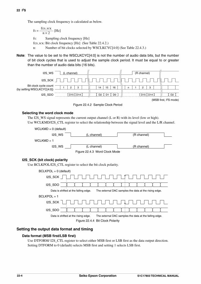
22 I2S
22-4 Seiko Epson Corporation S1C17803 TECHNICAL MANUAL
The sampling clock frequency is calculated as below.
fI2S_SCKfS = ———— [Hz] n × 2
fS: Sampling clock frequency [Hz]fI2S_SCK: Bit clock frequency [Hz] (See Table 22.4.2.)n: Number of bit clocks selected by WSCLKCYC[4:0] (See Table 22.4.3.)
Note: The value to be set to the WSCLKCYC[4:0] is not the number of audio data bits, but the number of bit clock cycles that is used to adjust the sample clock period. It must be equal to or greater than the number of audio data bits (16 bits).
1 2 3 14 15 16 n 1 2 3
D15 D2 D1 D0D14
I2S_WS
I2S_SCK
Bit clock cycle count(by setting WSCLKCYC[4:0])
I2S_SDO
(L channel) (R channel)
(MSB first, I2S mode)
D2D15 D14
Figure 22.4.2 Sample Clock Period
Selecting the word clock mode The I2S_WS signal represents the current output channel (L or R) with its level (low or high). Use WCLKMD/I2S_CTL register to select the relationship between the signal level and the L/R channel.
I2S_WS
WCLKMD = 0 (default)
(L channel) (R channel)
I2S_WS
WCLKMD = 1
(L channel) (R channel)
Figure 22.4.3 Word Clock Mode
I2S_SCK (bit clock) polarity Use BCLKPOL/I2S_CTL register to select the bit clock polarity.
I2S_SCK
I2S_SDO
BCLKPOL = 0 (default)
Data is shifted at the falling edge. The external DAC samples the data at the rising edge.
I2S_SCK
I2S_SDO
BCLKPOL = 1
Data is shifted at the rising edge. The external DAC samples the data at the falling edge.
Figure 22.4.4 Bit Clock Polarity
Setting the output data format and timing
Data format (MSB first/LSB first) Use DTFORM/ I2S_CTL register to select either MSB first or LSB first as the data output direction. Setting DTFORM to 0 (default) selects MSB first and setting 1 selects LSB first.

22 I2S
S1C17803 TECHNICAL MANUAL Seiko Epson Corporation 22-5
I2S_WS
I2S_SCK
I2S_SDO
DTFORM = 0 (default)
I2S_WS
I2S_SCK
I2S_SDO
DTFORM = 1
D0 D15 D2 D1 D0 D15 D14 D2 D1D14 D0
D15 D0 D13 D14 D15 D0 D1 D13 D14D1 D15
Figure 22.4.5 Output Data Format
Signed/unsigned format When right justified mode is selected as the data output timing condition, output data can be configured to
the signed or unsigned format using DTSIGN/I2S_CTL register. Setting DTSIGN to 0 (default) selects the unsigned format. The high-order bits that exceed the valid data
size are set to 0. Setting 1 selects the signed format. The high-order bits that exceed the valid data size are set to the sign bit value (D15) of the valid data.
I2S_WS
I2S_SCK
I2S_SDO
(L channel) (R channel)
0 D15 D2 D1 D0D14 0 D15 D14
(MSB first, right justified mode, number of bit clock cycles = 18)
DTSIGN = 0 (default)
I2S_WS
I2S_SCK
I2S_SDO
(L channel) (R channel)
D15 D2 D1 D0D14 D15 D14
DTSIGN = 1
Figure 22.4.6 Unsigned and Signed Format
This setting is effective only in right justified mode. Set DTSIGN to 0 when another data output timing mode is selected.
Data output timing Use DTTMG[1:0]/I2S_CTL register to select the data output timing.
Table 22.4.4 Data Output TimingDTTMG[1:0] Data output timing mode
0x3 Reserved0x2 Right justified mode0x1 Left justified mode0x0 I2S mode
(Default: 0x0)
When DTTMG[1:0] is set to 0x0 (default), I2S mode is selected. In this mode, the first bit of each data is output after one I2S_SCK clock delay from the I2S_WS signal edge.

22 I2S
22-6 Seiko Epson Corporation S1C17803 TECHNICAL MANUAL
1 2 3 14 15 16 1 2 3
I2S_WS
I2S_SCK
Bit clock cycle count(by setting WSCLKCYC[4:0])
I2S_SDO
(L channel) (R channel)
(MSB first, number of bit clock cycles = 18)
D15 D14 D15 D14
1817
D2D3 D1 D0
Figure 22.4.7 Data Output Timing 1 (I2S Mode)
When DTTMG[1:0] is set to 0x1, left justified mode is selected. In this mode, each data output starts at the I2S_WS signal edge.
1 2 3 14 15 16 1 2 3
I2S_WS
I2S_SCK
Bit clock cycle count(by setting WSCLKCYC[4:0])
I2S_SDO
(L channel) (R channel)
D15 D2 D1 D0D14 D13 D15 D14 D13
(MSB first, number of bit clock cycles = 18)
1817
Figure 22.4.8 Data Output Timing 2 (Left Justified Mode)
When DTTMG[1:0] is set to 0x2, right justified mode is selected. In this mode, output data is right justified to the I2S_WS signal edge.
1 2 3 4 5 16 1817 1 2 3 4 5
I2S_WS
I2S_SCK
Bit clock cycle count(by setting WSCLKCYC[4:0])
I2S_SDO
(L channel) (R channel)
(MSB first, number of bit clock cycles = 18)
D15 D2 D1 D0D0 D14 D13 D15 D14 D130 or D15 0 or D15
Figure 22.4.9 Data Output Timing 3 (Right Justified Mode)
Note: When using right justified mode, the number of bit clock cycles (sample clock period) must be equal to or greater than [Data bit size + 2].
22.5 Data Output ControlThe following shows audio data output procedure:
1. Set up the I2S conditions as described in the previous section.
2. Set up the interrupt or DMA conditions as described in Section 22.6.
3. Set the output channel mode using CHMD[1:0]/I2S_CTL register.
Table 22.5.1 Output Channel Mode Selection CHMD[1:0] Output channel mode L channel R channel
0x3 Mute 0 00x2 Mono (L) Data output 00x1 Mono (R) 0 Data output0x0 Stereo Data output Data output
(Default: 0x0)
The output channel mode can be switched even if data is being output. In this case, the mode changes after the current word output has finished.

22 I2S
S1C17803 TECHNICAL MANUAL Seiko Epson Corporation 22-7
4. Write the first audio data to the FIFO. The 16-bit register I2S_FIFO is used to write the output data to the FIFO. Up to four stereo data (16 bits × 2
channels (L & R) × 4) can be written to the FIFO. Before starting audio data output, fill the FIFO with the first four stereo data.
Use a 16-bit memory write (ld [%rb],%rs) instruction for writing data. Note that 8-bit and 24/32-bit mem-ory write instructions cannot be used. When the DMAC is used for writing, 16-bit or 32-bit access can be speci-fied.
First write L-channel data, then R-channel data. Both channel data must be written as a pair even if “mono” is selected as the output channel mode.
When four stereo data is written to the FIFO, the FIFO becomes full and I2SFIFOFF/I2S_FIFO_STAT register is set to 1. Note that the newest data of the FIFO is overwritten if data is written to I2S_FIFO in this status.
5. Write 1 to I2SOUTEN/I2S_CTL register to enable I2S output. When I2SOUTEN = 0, the I2S_MCLK and I2S_WS pins are fixed at 0. The I2S_SDO pin is left unchanged.
The I2S_SCK pin is fixed at 0 (when BCLKPOL/I2S_CTL register = 0) or 1 (when BCLKPOL = 1). When I2SOUTEN is set to 1, all output pins enter standby status.
6. Write 1 to I2SSTART/I2S_START register to start output. When I2SSTART is 0, the bit clock is stopped with pulled down to low. The word select clock is also stopped
with pulled up to high if WCLKMD = 0 or pulled down to low if WCLKMD = 1. When I2SSTART is set to 1, the I2S module loads one data (L & R) in the FIFO to the shift register and it starts
serial output in sync with the I2S_WS signal. The data in the shift register is shifted at the I2S_SCK clock edge and is output from the L channel first. When
an output of one data (L & R) has finished, the next data is read out from the FIFO and the same operation re-peats.
When the number of data according to the interrupt conditions has been read out from the FIFO, an interrupt can be generated.
When half empty interrupts are enabled, the I2S module generates an interrupt after two stereo data has been read out from the FIFO. In this case, write the next two stereo data (16 bits × 2 channels (L & R) × 2) to the FIFO.
When whole empty interrupts are enabled, the I2S module generates an interrupt after all data (four stereo data) has been read out from the FIFO. In this case, write the next four stereo data (16 bits × 2 channels (L & R) × 4) to the FIFO.
When one empty interrupts are enabled, the I2S module generates an interrupt after one stereo data has been read out from the FIFO. In this case, write the next one stereo data (16 bits × 2 channels (L & R) × 1) to the FIFO. This interrupt cause can also be used to invoke a DMA transfer.
I2SSTART
I2SBUSY
FIFO
I2S_WS pin
FIFOSTAT[2:0]
I2SFIFOFF
I2SFIFOEF
Interrupt
1, 2, 3, 4
2 2 431 30
1L 1R 2L 2R 3L 3R 4L 4R 5L 5R 6L 6R
Start
2, 3, 4 3, 4 5, 64, 5, 6
3, 4, 5, 6
6 EmptyEmpty
Half empty interrupt
Write 4 L & R data (1–4) Write 2 L & R data (5, 6)

22 I2S
22-8 Seiko Epson Corporation S1C17803 TECHNICAL MANUAL
I2SSTART
I2SBUSY
FIFO
I2S_WS pin
FIFOSTAT[2:0]
I2SFIFOFF
I2SFIFOEF
Interrupt
1, 2, 3, 4
4 2 33
2, 3, 4 3, 4 E4
5, 6, 7, 8
6, 7, 8 7, 8
Whole empty interrupt
Write 4 L & R data (1–4) Write 4 L & R data (5, 6, 7, 8)
1L 1R 2L 2R 3L 3R 4L 4R 5L 5R 6L 6R
Start
Write 4 L & R data (1–4)
210
Empty
43
5, 64, 5, 6 6 Empty
I2SSTART
I2SBUSY
FIFO
I2S_WS pin
FIFOSTAT[2:0]
I2SFIFOFF
I2SFIFOEF
Interrupt
1, 2, 3, 4
2 23 23
2, 3, 4
2, 3, 4, 5
One empty interrupt
Write 4 L & R data (1–4)Write 1 L & R data (5)
Write 1 L & R data (6)
3, 4, 5
3, 4, 5, 6
1L 1R 2L 2R 3L 3R 4L 4R 5L 5R 6L 6R
10
Start
Empty
Figure 22.5.1 FIFO Data and Interrupts
When the FIFO becomes empty, I2SFIFOEF/I2S_FIFO_STAT register is set to 1. When data is written to the FIFO, I2SFIFOEF is reset to 0 and the data output continues. Furthermore, the I2S provides the status bits FIFOSTAT[2:0]/I2S_FIFO_STAT register that indicate the FIFO
state machine.
Table 22.5.2 Monitoring the FIFO State MachineFIFOSTAT[2:0] State
0x7–0x6 Reserved0x5 FLUSH: FIFO is flushing the remained audio data before it stops.0x4 EMPTY: FIFO is empty.0x3 LACK: FIFO is not full and not empty.0x2 FULL: FIFO is full.0x1 INIT: Initialize all four entries of FIFO.0x0 STOP: FIFO is idle.
(Default: 0x0)
I2SBUSY/I2S_START register is set to 1 while data is being output. This flag can be used to check the output status.
7. To stop output, write 0 to I2SSTART/I2S_START register. When I2SSTART is set to 0, the I2S module will stop data output after the remaining data stored in the FIFO
are all output. When the I2S stops, I2SBUSY is reset to 0.
8. To disable output, write 0 to I2SOUTEN/I2S_CTL register after writing 0 to I2SSTART to stop the current out-put.
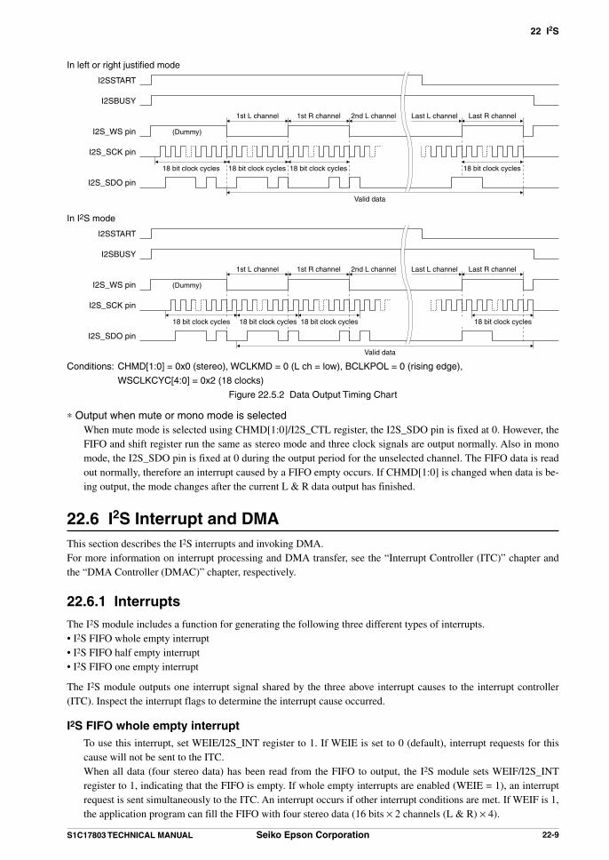
22 I2S
S1C17803 TECHNICAL MANUAL Seiko Epson Corporation 22-9
I2SSTART
I2SBUSY
I2S_WS pin
I2S_SCK pin
I2S_SDO pin
In left or right justified mode
18 bit clock cycles
Valid data
1st L channel
(Dummy)
1st R channel 2nd L channel Last R channelLast L channel
18 bit clock cycles 18 bit clock cycles 18 bit clock cycles
I2SSTART
I2SBUSY
I2S_WS pin
I2S_SCK pin
I2S_SDO pin
In I2S mode
Valid data
1st L channel
(Dummy)
1st R channel 2nd L channel Last R channelLast L channel
18 bit clock cycles 18 bit clock cycles 18 bit clock cycles 18 bit clock cycles
Conditions: CHMD[1:0] = 0x0 (stereo), WCLKMD = 0 (L ch = low), BCLKPOL = 0 (rising edge),
WSCLKCYC[4:0] = 0x2 (18 clocks)
Figure 22.5.2 Data Output Timing Chart
* Output when mute or mono mode is selected When mute mode is selected using CHMD[1:0]/I2S_CTL register, the I2S_SDO pin is fixed at 0. However, the
FIFO and shift register run the same as stereo mode and three clock signals are output normally. Also in mono mode, the I2S_SDO pin is fixed at 0 during the output period for the unselected channel. The FIFO data is read out normally, therefore an interrupt caused by a FIFO empty occurs. If CHMD[1:0] is changed when data is be-ing output, the mode changes after the current L & R data output has finished.
22.6 I2S Interrupt and DMAThis section describes the I2S interrupts and invoking DMA.For more information on interrupt processing and DMA transfer, see the “Interrupt Controller (ITC)” chapter and the “DMA Controller (DMAC)” chapter, respectively.
22.6.1 Interrupts
The I2S module includes a function for generating the following three different types of interrupts.• I2S FIFO whole empty interrupt • I2S FIFO half empty interrupt • I2S FIFO one empty interrupt
The I2S module outputs one interrupt signal shared by the three above interrupt causes to the interrupt controller (ITC). Inspect the interrupt flags to determine the interrupt cause occurred.
I2S FIFO whole empty interrupt To use this interrupt, set WEIE/I2S_INT register to 1. If WEIE is set to 0 (default), interrupt requests for this
cause will not be sent to the ITC. When all data (four stereo data) has been read from the FIFO to output, the I2S module sets WEIF/I2S_INT
register to 1, indicating that the FIFO is empty. If whole empty interrupts are enabled (WEIE = 1), an interrupt request is sent simultaneously to the ITC. An interrupt occurs if other interrupt conditions are met. If WEIF is 1, the application program can fill the FIFO with four stereo data (16 bits × 2 channels (L & R) × 4).

22 I2S
22-10 Seiko Epson Corporation S1C17803 TECHNICAL MANUAL
I2S FIFO half empty interrupt To use this interrupt, set HEIE/I2S_INT register to 1. If HEIE is set to 0 (default), interrupt requests for this
cause will not be sent to the ITC. When a free space for two stereo data becomes available in the FIFO, the I2S module sets HEIF/I2S_INT regis-
ter to 1. If half empty interrupts are enabled (HEIE = 1), an interrupt request is sent simultaneously to the ITC. An interrupt occurs if other interrupt conditions are met. If HEIF is 1, the application program can fill the FIFO with two stereo data (16 bits × 2 channels (L & R) × 2).
I2S FIFO one empty interrupt To use this interrupt, set OEIE/I2S_INT register to 1. If OEIE is set to 0 (default), interrupt requests for this
cause will not be sent to the ITC. When a free space for one stereo data becomes available in the FIFO, the I2S module sets OEIF/I2S_INT regis-
ter to 1. If one empty interrupts are enabled (OEIE = 1), an interrupt request is sent simultaneously to the ITC. An interrupt occurs if other interrupt conditions are met. If OEIF is 1, the application program can fill the FIFO with one stereo data (16 bits × 2 channels (L & R) × 1).
For more information on interrupt processing, see the “Interrupt Controller (ITC)” chapter.
Note: Fill the FIFO with four stereo data (16 bits × 2 channels (L & R) × 4) at the beginning of transfer via I2S (at the time of start by setting I2SSTART to 1) regardless of the interrupt condition.
• When filling the FIFO before enabling the interrupt Write four stereo data to the FIFO, then enable the interrupt. When a FIFO empty interrupt oc-
curs, the interrupt handler routine must write one, two or four stereo data to the FIFO according to the interrupt used.
• When filling the FIFO after enabling the interrupt Just write one, two or four stereo data to the FIFO according to the interrupt used.
22.6.2 DMA Transfer
The cause of one empty interrupt can invoke a DMA. This allows continuous data output through DMA transfer be-tween memory and the FIFO. The interrupt signal is output to both the ITC and DMAC. Therefore, DMA transfer can be performed without generating any I2S interrupt.The following lists the DMA channels that allow selection of the I2S one-empty interrupt cause as the trigger.
DMAC Ch.0: Used for L and R data transfer with single DMA, or L data transfer with dual DMA.DMAC Ch.1: Used for L and R data transfer with single DMA, or R data transfer with dual DMA.DMAC Ch.3: Used for L and R data transfer with single DMA.
Use one or two DMAC channels according to the audio data storing method.When L-channel and R-channel audio data are sequentially stored in a memory area, use a DMAC channel and perform 32-bit data transfer to write both L (low-order 16 bits) and R (high-order 16 bits) data to the FIFO (fixed address 0x81510) for each DMA request. Note that 16-bit and 8-bit data transfer cannot be specified.
When L-channel and R-channel audio data are stored in different locations, use DMAC Ch.0 and Ch.1. In this case, perform 16-bit data transfer to write L-channel data to the FIFO (fixed address 0x81510) using DMAC Ch.0 and to write R-channel data to the FIFO (fixed address 0x81512) using Ch.1. The I2S one-empty DMA request is sent to DMAC Ch.0 and Ch.1 simultaneously. However, DMAC Ch.0 starts a DMA transfer first as it priority over Ch.1. Therefore, DMAC Ch.0 must be used for L-channel data transfer. Note that 8-bit and 32-bit data transfer cannot be specified when dual DMA channels are used.
For more information on DMA transfer, see the “DMA Controller (DMAC)” chapter.

22 I2S
S1C17803 TECHNICAL MANUAL Seiko Epson Corporation 22-11
22.7 Control Register Details
Table 22.7.1 List of I2S RegistersAddress Register name Function0x81500 I2S_CTL I2S Control Register Sets the I2S output conditions.0x81504 I2S_DV_MCLK I2S Master Clock Division ratio Register Configures the master clock.
0x81506 I2S_DV_AUDIO_CLK I2S Audio Clock Division ratio Register Configures the audio clock.0x81508 I2S_START I2S Start/Stop Register Controls/indicates I2S start/stop status.0x8150a I2S_FIFO_STAT I2S FIFO Status Register Indicates the FIFO status.0x8150c I2S_INT I2S Interrupt Control Register Controls I2S interrupts.0x81510 I2S_FIFO I2S FIFO Register L-channel output data0x81512 R-channel output data
The following describes each I2S register. These are all 16-bit registers.
Note: When data is written to the registers, the “Reserved” bits must always be written as 0 and not 1.
I2S Control Register (I2S_CTL)Register name Address Bit Name Function Setting Init. R/W Remarks
I2S Control Register (I2S_CTL)
0x81500(16 bits)
D15–9 – reserved – – – 0 when being read.D8 DTSIGN I2S signed/unsigned data format
select1 Signed 0 Unsigned 0 R/W
D7 WCLKMD I2S output word clock mode select 1 L: HighR: Low
0 L: LowR: High
0 R/W
D6 BCLKPOL I2S output bit clock polarity select 1 Negative 0 Positive 0 R/WD5 DTFORM I2S output data format select 1 LSB first 0 MSB first 0 R/WD4 I2SOUTEN I2S output enable 1 Enable 0 Disable 0 R/W
D3–2 DTTMG[1:0] I2S output data timing select DTTMG[1:0] Timing mode 0x0 R/W0x30x20x10x0
reservedRight justifiedLeft justified
I2SD1–0 CHMD[1:0] I2S output channel mode select CHMD[1:0] Channel mode 0x0 R/W
0x30x20x10x0
MuteMono left
Mono rightStereo
Note: All the data transfer conditions must be set using this register before setting I2SSTART/I2S_START register to start data output from the I2S module.
D[15:9] Reserved
D8 DTSIGN: I2S Signed/Unsigned Data Format Select Bit Selects the data format in right justified mode. 1 (R/W): Signed 0 (R/W): Unsigned (default)
Setting DTSIGN to 0 (default) selects the unsigned format. The high-order bits that exceed the valid data size are set to 0. Setting 1 selects the signed format. The high-order bits that exceed the valid data size are set to the sign bit value (D15) of the valid data.
This setting is effective only in right justified mode. Set DTSIGN to 0 when another data output timing mode is selected.
I2S_WS
I2S_SCK
I2S_SDO
I2S_SDO
(L channel) (R channel)
0 D15 D2 D1 D0D14 0 D15 D14
(MSB first, right justified mode, number of bit clock cycles = 18)
D15 D2 D1 D0D14 D15 D14
DTSIGN = 0 (default)
DTSIGN = 1
Figure 22.7.1 Unsigned and Signed Format

22 I2S
22-12 Seiko Epson Corporation S1C17803 TECHNICAL MANUAL
D7 WCLKMD: I2S Output Word Clock Mode Select Bit Selects the I2S_WS output signal level for indicating a channel. 1 (R/W): High = L channel, Low = R channel 0 (R/W): High = R channel, Low = L channel (default)
I2S_WS0
WCLKMD = 0 (default)
(L channel) (R channel)
I2S_WS0
WCLKMD = 1
(L channel) (R channel)
Figure 22.7.2 Word Clock Mode
D6 BCLKPOL: I2S Output Bit Clock Polarity Select Bit Selects the bit clock polarity. 1 (R/W): Negative 0 (R/W): Positive (default)
When BCLKPOL is 0, the I2S_SDO output changes at the falling edge of the I2S_SCK clock (bit clock) and the external DAC samples the data bit at the rising edge of I2S_SCK.
When BCLKPOL is set to 1, the I2S_SDO output changes at the rising edge of I2S_SCK and the exter-nal DAC samples the data bit at the falling edge of I2S_SCK.
I2S_SCK
I2S_SDO
BCLKPOL = 0 (default)
Data is shifted at the falling edge. The external DAC samples the data at the rising edge.
I2S_SCK
I2S_SDO
BCLKPOL = 1
Data is shifted at the rising edge. The external DAC samples the data at the falling edge.
Figure 22.7.3 Bit Clock Polarity
D5 DTFORM: I2S Output Data Format Select Bit Selects either MSB first or LSB first as the data output direction. 1 (R/W): LSB first 0 (R/W): MSB first (default)
I2S_WS
I2S_SCK
I2S_SDO
DTFORM = 0 (default)
I2S_WS
I2S_SCK
I2S_SDO
DTFORM = 1
D0 D15 D2 D1 D0 D15 D14 D2 D1D14 D0
D15 D0 D13 D14 D15 D0 D1 D13 D14D1 D15
Figure 22.7.4 Output Data Format
D4 I2SOUTEN: I2S Output Enable Bit Enables/disables output of the I2S signals. 1 (R/W): Enable (on) 0 (R/W): Disable (off) (default)

22 I2S
S1C17803 TECHNICAL MANUAL Seiko Epson Corporation 22-13
When I2SOUTEN = 0, the I2S_MCLK and I2S_WS pins are fixed at 0. The I2S_SDO pin is left un-changed. The I2S_SCK pin is fixed at 0 (when BCLKPOL/I2S_CTL register = 0) or 1 (when BCLK-POL = 1).
When I2SOUTEN is set to 1, all output pins enter standby status.
D[3:2] DTTMG[1:0]: I2S Output Data Timing Select Bits Selects the data bit output timing.
Table 22.7.2 Data Output TimingDTTMG[1:0] Data output timing mode
0x3 Reserved0x2 Right justified mode0x1 Left justified mode0x0 I2S mode
(Default: 0x0)
When DTTMG[1:0] is set to 0x0 (default), I2S mode is selected. In this mode, the first bit of each data is output after one I2S_SCK clock delay from the I2S_WS signal edge.
1 2 3 14 15 16 1 2 3
I2S_WS
I2S_SCK
Bit clock cycle count(by setting WSCLKCYC[4:0])
I2S_SDO
(L channel) (R channel)
(MSB first, number of bit clock cycles = 18)
D15 D2D3 D1 D0D14 D15 D14
1817
Figure 22.7.5 Data Output Timing 1 (I2S Mode)
When DTTMG[1:0] is set to 0x1, left justified mode is selected. In this mode, each data output will start at the I2S_WS signal edge.
1 2 3 14 15 16 1 2 3
I2S_WS
I2S_SCK
Bit clock cycle count(by setting WSCLKCYC[4:0])
I2S_SDO
(L channel) (R channel)
D15 D2 D1 D0D14 D13 D15 D14 D13
(MSB first, number of bit clock cycles = 18)
1817
Figure 22.7.6 Data Output Timing 2 (Left Justified Mode)
When DTTMG[1:0] is set to 0x2, right justified mode is selected. In this mode, output data will be right justified to the I2S_WS signal edge.
1 2 3 4 5 16 1817 1 2 3 4 5
I2S_WS
I2S_SCK
Bit clock cycle count(by setting WSCLKCYC[4:0])
I2S_SDO
(L channel) (R channel)
(MSB first, number of bit clock cycles = 18)
D15 D2 D1 D0D0 D14 D13 D15 D14 D130 or D15 0 or D15
Figure 22.7.7 Data Output Timing 3 (Right Justified Mode)
Note: When using right justified mode, the number of bit clock cycles (sample clock period) must be equal to or greater than [Data bit size + 2].
D[1:0] CHMD[1:0]: I2S Output Channel Mode Select Bits Selects the I2S output channel mode.

22 I2S
22-14 Seiko Epson Corporation S1C17803 TECHNICAL MANUAL
Table 22.7.3 Output Channel Mode SelectionCHMD[1:0] Output channel mode L channel R channel
0x3 Mute 0 00x2 Mono (L) Data output 00x1 Mono (R) 0 Data output0x0 Stereo Data output Data output
(Default: 0x0)
The output channel mode can be switched even if data is being output. In this case, the mode changes after the current word output has finished.
When mute mode is selected, the I2S_SDO pin is fixed at 0. However, the FIFO and shift register run the same as stereo mode and three clock signals are output normally. Also in mono mode, the I2S_SDO pin is fixed at 0 during the output period for the unselected channel.
The FIFO data is read out normally, therefore an interrupt occurs.
I2S Master Clock Division Ratio Register (I2S_DV_MCLK)Register name Address Bit Name Function Setting Init. R/W Remarks
I2S Master Clock Division Ratio Register (I2S_DV_MCLK)
0x81504(16 bits)
D15–6 – reserved – – – 0 when being read.D5–0 MCLKDIV
[5:0]I2S_MCLK division ratio select MCLKDIV[5:0] I2S_MCLK 0x0 R/W
0x3f0x3e0x3d
:0x20x10x0
PCLK1•1/64PCLK1•1/63PCLK1•1/62
:PCLK1•1/3PCLK1•1/2PCLK1•1/1
D[15:6] Reserved
D[5:0] MCLKDIV[5:0]: I2S_MCLK Division Ratio Select Bits Configures the I2S master clock (I2S_MCLK) to be output from the I2S_MCLK pin. The I2S module generates the I2S_MCLK by dividing the operating clock (PCLK1 generated by the
CMU). Specify the division ratio using MCLKDIV[5:0].
Table 22.7.4 I2S_MCLK (Master Clock) SettingsMCLKDIV[5:0] I2S_MCLK
0x3f PCLK1•1/640x3e PCLK1•1/630x3d PCLK1•1/62
: :0x2 PCLK1•1/30x1 PCLK1•1/20x0 PCLK1•1/1
(Default: 0x0)
I2S Audio Clock Division Ratio Register (I2S_DV_AUDIO_CLK)Register name Address Bit Name Function Setting Init. R/W Remarks
I2S Audio Clock Division Ratio Register (I2S_DV_AUDIO_CLK)
0x81506(16 bits)
D15–13 – reserved – – – 0 when being read.D12–8 WSCLKCYC
[4:0]I2S WS clock cycle setup WSCLKCYC[4:0] Clock period 0x0 R/W
0x1f–0x110x100xf0xe0xd0xc0xb0xa0x90x80x70x60x50x40x30x20x10x0
reserved32 clocks31 clocks30 clocks29 clocks28 clocks27 clocks26 clocks25 clocks24 clocks23 clocks22 clocks21 clocks20 clocks19 clocks18 clocks17 clocks16 clocks

22 I2S
S1C17803 TECHNICAL MANUAL Seiko Epson Corporation 22-15
I2S Audio Clock Division Ratio Register (I2S_DV_AUDIO_CLK)
0x81506(16 bits)
D7–0 BCLKDIV[7:0]
I2S bit clock division ratio select BCLKDIV[7:0] Bit clock 0x0 R/W0xff0xfe0xfd
:0x20x10x0
PCLK1•1/512PCLK1•1/510PCLK1•1/508
:PCLK1•1/6PCLK1•1/4PCLK1•1/2
D[15:13] Reserved
D[12:8] WSCLKCYC[4:0]: I2S WS Clock Cycle Setup Bits Specifies the sample clock (I2S_WS signal) period. The I2S generates the sample clock to be output from the I2S_WS pin by counting the bit clock config-
ured with BCLKDIV[7:0]. Specify the half cycle (a high or low level period) of the I2S_WS clock with the number of bit clock cycles using WSCLKCYC[4:0].
Table 22.7.5 Sample Clock Settings
WSCLKCYC[4:0]Sample clock period
(number of bit clock cycles)0x1f–0x11 Reserved
0x10 32 clocks0xf 31 clocks0xe 30 clocks0xd 29 clocks0xc 28 clocks0xb 27 clocks0xa 26 clocks0x9 25 clocks0x8 24 clocks0x7 23 clocks0x6 22 clocks0x5 21 clocks0x4 20 clocks0x3 19 clocks0x2 18 clocks0x1 17 clocks0x0 16 clocks
(Default: 0x0)
The sampling clock frequency is calculated as below.
fI2S_SCKfS = ———— [Hz] n × 2
fS: Sampling clock frequency [Hz]fI2S_SCK: Bit clock frequency [Hz] (See Table 22.7.6.)n: Number of bit clocks selected by WSCLKCYC[4:0] (See Table 22.7.5.)
Note: The value to be set to the WSCLKCYC[4:0] is not the number of audio data bits, but the num-ber of bit clock cycles that is used to adjust the sample clock period. It must be equal to or greater than the number of audio data bits (16 bits).
1 2 3 14 15 16 n 1 2 3
D15 D2 D1 D0D14
I2S_WS
I2S_SCK
Bit clock cycle count(by setting WSCLKCYC[4:0])
I2S_SDO
(L channel) (R channel)
(MSB first, I2S mode)
D2D15 D14
Figure 22.7.8 Sample Clock Period

22 I2S
22-16 Seiko Epson Corporation S1C17803 TECHNICAL MANUAL
D[7:0] BCLKDIV[7:0]: I2S Bit Clock Division ratio Select Bits Configures the bit clock to be output. The I2S module generates the bit clock to be output from the I2S_SCK pin of the I2S by dividing
PCLK1. Specify the division ratio using BCLKDIV[7:0].
Table 22.7.6 Setting Output Bit ClockBCLKDIV[7:0] Bit clock (I2S_SCK)
0xff PCLK1•1/5120xfe PCLK1•1/5100xfd PCLK1•1/508
: :0x2 PCLK1•1/60x1 PCLK1•1/40x0 PCLK1•1/2
(Default: 0x0)
The I2S bit clock frequency is calculated as below.
fPCLK1fI2S_SCK = ————————— [Hz] (BCLKDIV + 1) × 2
fI2S_SCK: I2S bit clock frequency [Hz]fPCLK1: PCLK1clock frequency [Hz]BCLKDIV: BCLKDIV[7:0] set value (0x0–0xff)
I2S Start/Stop Register (I2S_START)Register name Address Bit Name Function Setting Init. R/W Remarks
I2S Start/Stop Register (I2S_START)
0x81508(16 bits)
D15–8 – reserved – – – 0 when being read.D7 I2SBUSY I2S busy flag 1 Busy 0 Idle 0 R
D6–1 – reserved – – – 0 when being read.D0 I2SSTART I2S start/stop control 1 Start (run) 0 Stop 0 R/W
D[15:8] Reserved
D7 I2SBUSY: I2S Busy Flag Bit Indicates the data output status of the I2S module. 1 (R): Busy 0 (R): Idle (default)
I2SBUSY is set to 1 when the I2S starts data output and stays 1 while data is being output. This flag is cleared to 0 upon completion of the output operation.
D[6:1] Reserved
D0 I2SSTART: I2S Start/Stop Control Bit Starts/stops data output of the I2S. 1 (R/W): Start 0 (R/W): Stop (default) Writing 1 to I2SSTART starts serial data transmission through the I2S_SDO pin. Writing 0 to I2SSTART stops data transmission. Note, however, that the data currently stored in the
FIFO will be continuously transmitted through the I2S_SDO pin until the FIFO becomes empty. After I2SSTART is set to 0, new transmit data cannot be written to the FIFO.
Note: Be sure to avoid altering the I2S_DV_MCLK and I2S_DV_AUDIO_CLK registers when I2SSTART is 1.

22 I2S
S1C17803 TECHNICAL MANUAL Seiko Epson Corporation 22-17
I2S FIFO Status Register (I2S_FIFO_STAT)Register name Address Bit Name Function Setting Init. R/W Remarks
I2S FIFO Status Register (I2S_FIFO_STAT)
0x8150a(16 bits)
D15–5 – reserved – – – 0 when being read.D4–2 FIFOSTAT
[2:0]I2S FIFO state machine FIFOSTAT[2:0] State 0x0 R
0x7–0x60x50x40x30x20x10x0
reservedFLUSHEMPTYLACKFULLINIT
STOPD1 I2SFIFOFF I2S FIFO full flag 1 Full 0 Not full 0 RD0 I2SFIFOEF I2S FIFO empty flag 1 Empty 0 Not empty 1 R
D[15:5] Reserved
D[4:2] FIFOSTAT[2:0]: I2S FIFO State Machine Bits Indicates the transmit FIFO status.
Table 22.7.7 Monitoring the FIFO State MachineFIFOSTAT[2:0] State
0x7–0x6 Reserved0x5 FLUSH: FIFO is flushing the remained audio data before it stops.0x4 EMPTY: FIFO is empty.0x3 LACK: FIFO is not full and not empty.0x2 FULL: FIFO is full.0x1 INIT: Initialize all four entries of FIFO.0x0 STOP: FIFO is idle.
(Default: 0x0)
D1 I2SFIFOFF: I2S FIFO Full Flag Bit Indicates whether the transmit FIFO is full or not. 1 (R): Full 0 (R): Not full (default)
I2SFIFOFF is set to 1 when the FIFO becomes full of the written data (16 bits × 2 channels (L & R) × 4) to indicate that no more data can be written.
I2SFIFOFF is reset to 0 when the stored data is read out to transmit.
D0 I2SFIFOEF: I2S FIFO Empty Flag Bit Indicates whether the transmit FIFO is empty or not. 1 (R): Empty (default) 0 (R): Not empty
I2SFIFOEF is reset to 0 when a transmit data is written to the FIFO and is set to 1 when all the stored data have been transmitted.
I2S Interrupt Control Register (I2S_INT)Register name Address Bit Name Function Setting Init. R/W Remarks
I2S Interrupt Control Register (I2S_INT)
0x8150c(16 bits)
D15–11 – reserved – – – 0 when being read.D10 WEIF I2S FIFO whole empty int. flag 1 Cause of
interrupt occurred
0 Cause of interrupt not occurred
0 R/W Reset by writing 1.D9 HEIF I2S FIFO half empty interrupt flag 1 0 0 R/WD8 OEIF I2S FIFO one empty interrupt flag 1 0 0 R/W
D7–3 – reserved – – – 0 when being read.D2 WEIE I2S FIFO whole empty int. enable 1 Enable 0 Disable 0 R/WD1 HEIE I2S FIFO half empty int. enable 1 Enable 0 Disable 0 R/WD0 OEIE I2S FIFO one empty int. enable 1 Enable 0 Disable 0 R/W
D[15:11] Reserved

22 I2S
22-18 Seiko Epson Corporation S1C17803 TECHNICAL MANUAL
D10 WEIF: I2S FIFO Whole Empty Interrupt Flag Bit Indicates whether the cause of I2S FIFO whole empty interrupt has occurred or not. 1 (R): Cause of interrupt has occurred 0 (R): No cause of interrupt has occurred (default) 1 (W): Flag is reset 0 (W): Ignored
When all data (four stereo data) has been read from the FIFO to transmit, the I2S module sets WEIF to 1, indicating that the FIFO is empty. If I2S FIFO whole empty interrupts are enabled (WEIE = 1), an inter-rupt request is sent simultaneously to the ITC. If WEIF is 1, the application program can fill the FIFO with four stereo data (16 bits × 2 channels (L & R) × 4). WEIF is reset by writing 1.
D9 HEIF: I2S FIFO Half Empty Interrupt Flag Bit Indicates whether the cause of I2S FIFO half empty interrupt has occurred or not. 1 (R): Cause of interrupt has occurred 0 (R): No cause of interrupt has occurred (default) 1 (W): Flag is reset 0 (W): Ignored
When a free space for two stereo data becomes available in the FIFO, the I2S module sets HEIF to 1. If I2S FIFO half empty interrupts are enabled (HEIE = 1), an interrupt request is sent simultaneously to the ITC. If HEIF is 1, the application program can fill the FIFO with two stereo data (16 bits × 2 chan-nels (L & R) × 2). HEIF is reset by writing 1.
D8 OEIF: I2S FIFO One Empty Interrupt Flag Bit Indicates whether the cause of I2S FIFO one empty interrupt has occurred or not. 1 (R): Cause of interrupt has occurred 0 (R): No cause of interrupt has occurred (default) 1 (W): Flag is reset 0 (W): Ignored
When a free space for one stereo data becomes available in the FIFO, the I2S module sets OEIF to 1. If I2S FIFO one empty interrupts are enabled (OEIE = 1), an interrupt request is sent simultaneously to the ITC. If OEIF is 1, the application program can fill the FIFO with one stereo data (16 bits × 2 channels (L & R) × 1). OEIF is reset by writing 1.
D[7:3] Reserved
D2 WEIE: I2S FIFO Whole Empty Interrupt Enable Bit Enables or disables I2S FIFO whole empty interrupts. 1 (R/W): Interrupt enabled 0 (R/W): Interrupt disabled (default)
Setting WEIE to 1 enables I2S FIFO whole empty interrupt requests to the ITC. Setting it to 0 disables interrupts.
D1 HEIE: I2S FIFO Half Empty Interrupt Enable Bit Enables or disables I2S FIFO half empty interrupts. 1 (R/W): Interrupt enabled 0 (R/W): Interrupt disabled (default)
Setting HEIE to 1 enables I2S FIFO half empty interrupt requests to the ITC. Setting it to 0 disables in-terrupts.
D0 OEIE: I2S FIFO One Empty Interrupt Enable Bit Enables or disables I2S FIFO one empty interrupts. 1 (R/W): Interrupt enabled 0 (R/W): Interrupt disabled (default)
Setting OEIE to 1 enables I2S FIFO one empty interrupt requests to the ITC. Setting it to 0 disables in-terrupts.

22 I2S
S1C17803 TECHNICAL MANUAL Seiko Epson Corporation 22-19
I2S FIFO Register (I2S_FIFO)Register name Address Bit Name Function Setting Init. R/W Remarks
I2S FIFO Register (I2S_FIFO)
0x81510(16 bits)
D15–0 I2SFIFO[15:0]
I2S FIFO (L-channel output data) 0 to 0xffff 0x0 W 0 when being read.
0x81512(16 bits)
D15–0 I2S FIFO (R-channel output data)
D[15:0] I2SFIFO[15:0]: I2S FIFO (Output Data) Bits Write output data to the FIFO through this address. Up to four stereo data (16 bits × 2 channels (L & R) × 4) can be written to the FIFO. Before starting au-
dio data output, fill the FIFO with the first four stereo data.
When writing data in the interrupt handler routineWhen writing data in the interrupt handler routine, use a 16-bit memory write (ld [%rb],%rs) instruction. Note that 8-bit and 24/32-bit memory write instructions cannot be used.First write L-channel data to address 0x81510, then R-channel data to address 0x81512. Both chan-nel data must be written as a pair even if “mono” is selected as the output channel mode.Write the first to fourth data to the same addresses (0x81510, 0x81512) without changing.
When writing data via DMACWhen L-channel and R-channel audio data are sequentially stored in a memory area, use a DMAC channel (Ch.0, Ch.1, or Ch.3) and perform 32-bit data transfer to write both L (low-order 16 bits) and R (high-order 16 bits) data to address 0x81510 (fixed) for each DMA request. Note that 16-bit and 8-bit data transfer cannot be specified.When L-channel and R-channel audio data are stored in different locations, use DMAC Ch.0 and Ch.1. In this case, perform 16-bit data transfer to write L-channel data to address 0x81510 (fixed) using DMAC Ch.0 and to write R-channel data to address 0x81512 (fixed) using Ch.1. The I2S one-empty DMA request is sent to DMAC Ch.0 and Ch.1 simultaneously. However, DMAC Ch.0 starts a DMA transfer first as it priority over Ch.1. Therefore, DMAC Ch.0 must be used for L-channel data transfer. Note that 8-bit and 32-bit data transfer cannot be specified when dual DMA channels are used.
22.8 Setting the I2S ClocksThis section explains how to configure the I2S_MCLK, I2S_WS, and I2S_SCK clocks.The following shows how to determine the clock setting values from the sampling rate. The example below as-sumes that the system clock frequency is 33 MHz and the sampling rate of audio data is 44.1 kHz.The sample clock (I2S_WS) is in sync with the master clock (I2S_MCLK), so the following equation is formu-lated:
fI2S_MCLK ————— = Integer fI2S_WS
where fI2S_MCLK is the output master clock (I2S_MCLK) frequency and fI2S_WS is the sample clock (I2S_WS) frequency.
33 MHz fI2S_MCLK = ————————— (eq1) MCLKDIV[5:0] + 1
33 MHz fI2S_WS = ————— ————— ——————————————— (eq2) (BCLKDIV[7:0] + 1) × 2 × (WSCLKCYC[4:0] + 16 ) × 2
(BCLKDIV[7:0] + 1) × 2 × (WSCLKCYC[4:0] + 16 ) × 2 ————————————————————————— = Integer (eq3) MCLKDIV[5:0] + 1

22 I2S
22-20 Seiko Epson Corporation S1C17803 TECHNICAL MANUAL
Table 22.8.1 I2S_MCLK (Master Clock) SettingsMCLKDIV[5:0] I2S_MCLK
0x3f PCLK1•1/640x3e PCLK1•1/630x3d PCLK1•1/62
: :0x2 PCLK1•1/30x1 PCLK1•1/20x0 PCLK1•1/1
Table 22.8.2 Bit Clock Settings BCLKDIV[7:0] Bit clock (I2S_SCK)
0xff PCLK1•1/5120xfe PCLK1•1/5100xfd PCLK1•1/508
: :0x2 PCLK1•1/60x1 PCLK1•1/40x0 PCLK1•1/2
Table 22.8.3 Sample Clock Period Settings
WSCLKCYC[4:0]Sample clock period
(number of bit clock cycles)0x1f–0x11 Reserved
0x10 32 clocks0xf 31 clocks0xe 30 clocks0xd 29 clocks0xc 28 clocks0xb 27 clocks0xa 26 clocks0x9 25 clocks0x8 24 clocks0x7 23 clocks0x6 22 clocks0x5 21 clocks0x4 20 clocks0x3 19 clocks0x2 18 clocks0x1 17 clocks0x0 16 clocks

22 I2S
S1C17803 TECHNICAL MANUAL Seiko Epson Corporation 22-21
The table below is made from Equitation 2 (eq2) using Excel.
Table 22.8.4 List of Sample Clock FrequenciesA B C D E F G H I J K L M N O P Q R S
1 SysClk[kHz]
BCLKDIV[7:0]WSCLKCYC[4:0]
2 0 1 2 3 4 5 6 7 8 9 10 11 12 13 14 15 163 33000 0 515.63 485.29 458.33 434.21 412.50 392.86 375.00 358.70 343.75 330.00 317.31 305.56 294.64 284.48 275.00 266.13 257.81 4 1 257.81 242.65 229.17 217.11 206.25 196.43 187.50 179.35 171.88 165.00 158.65 152.78 147.32 142.24 137.50 133.06 128.91 5 2 171.88 161.76 152.78 144.74 137.50 130.95 125.00 119.57 114.58 110.00 105.77 101.85 98.21 94.83 91.67 88.71 85.94 6 3 128.91 121.32 114.58 108.55 103.13 98.21 93.75 89.67 85.94 82.50 79.33 76.39 73.66 71.12 68.75 66.53 64.45 7 4 103.13 97.06 91.67 86.84 82.50 78.57 75.00 71.74 68.75 66.00 63.46 61.11 58.93 56.90 55.00 53.23 51.56 8 5 85.94 80.88 76.39 72.37 68.75 65.48 62.50 59.78 57.29 55.00 52.88 50.93 49.11 47.41 45.83 44.35 42.97 9 6 73.66 69.33 65.48 62.03 58.93 56.12 53.57 51.24 49.11 47.14 45.33 43.65 42.09 40.64 39.29 38.02 36.83 10 7 64.45 60.66 57.29 54.28 51.56 49.11 46.88 44.84 42.97 41.25 39.66 38.19 36.83 35.56 34.38 33.27 32.23 11 8 57.29 53.92 50.93 48.25 45.83 43.65 41.67 39.86 38.19 36.67 35.26 33.95 32.74 31.61 30.56 29.57 28.65 12 9 51.56 48.53 45.83 43.42 41.25 39.29 37.50 35.87 34.38 33.00 31.73 30.56 29.46 28.45 27.50 26.61 25.78 13 10 46.88 44.12 41.67 39.47 37.50 35.71 34.09 32.61 31.25 30.00 28.85 27.78 26.79 25.86 25.00 24.19 23.44 14 11 42.97 40.44 38.19 36.18 34.38 32.74 31.25 29.89 28.65 27.50 26.44 25.46 24.55 23.71 22.92 22.18 21.48 15 12 39.66 37.33 35.26 33.40 31.73 30.22 28.85 27.59 26.44 25.38 24.41 23.50 22.66 21.88 21.15 20.47 19.83 16 13 36.83 34.66 32.74 31.02 29.46 28.06 26.79 25.62 24.55 23.57 22.66 21.83 21.05 20.32 19.64 19.01 18.42 17 14 34.38 32.35 30.56 28.95 27.50 26.19 25.00 23.91 22.92 22.00 21.15 20.37 19.64 18.97 18.33 17.74 17.19 18 15 32.23 30.33 28.65 27.14 25.78 24.55 23.44 22.42 21.48 20.63 19.83 19.10 18.42 17.78 17.19 16.63 16.11 : : : : : : : : : : : : : : : : : : : :
257 254 2.02 1.90 1.80 1.70 1.62 1.54 1.47 1.41 1.35 1.29 1.24 1.20 1.16 1.12 1.08 1.04 1.01 258 255 2.01 1.90 1.79 1.70 1.61 1.53 1.46 1.40 1.34 1.29 1.24 1.19 1.15 1.11 1.07 1.04 1.01
Cell [A3]: System clock frequency (33000 kHz)Cells [B3:B258]: BCLKDIV[7:0] settings (0 to 255)Cells [C2:S2]: WSCLKCYC[4:0] settings (0 to 16)Cells [C3:S258]: fI2S_WS calculated by Equation 2 (eq2) according to the BCLKDIV[7:0] and WSCLKCYC[4:0] settings Cell [C3] = $A$3/(($B3+1)*2*(C$2+16)*2) Cell [S3] = $A$3/(($B3+1)*2*(S$2+16)*2) : : Cell [C258] = $A$3/(($B258+1)*2*(C$2+16)*2) Cell [S258] = $A$3/(($B258+1)*2*(S$2+16)*2)
If you use another system clock frequency, enter the frequency in kHz to Cell [A3]. Cells [C3:S258] will be cor-rected according to the entered value.
Find “44.1 (kHz)” or an approximate value from the table. You may choose “44.12” in Cell [D13].You may get the BCLKDIV[7:0] and WSCLKCYC[4:0] values as 10 and 1, respectively.
Substituting these values in Equation 3 (eq3) yields the MCLKDIV[5:0] values.
(10 + 1) × 2 × (1 + 16) × 2 ————— ——————— = Integer MCLKDIV[5:0] + 1
The table below is made from Equitation 3 (eq3) using Excel.
Table 22.8.5 MCLKDIV[5:0] Valid ValuesU V
1 BCLKDIV[7:0] WSCLKCYC[4:0]2 10 134 MCLKDIV[5:0] Results5 0 Integer6 1 Integer7 2 –8 3 Integer9 4 –: : –
15 10 Integer: : –
21 16 Integer: : –
26 21 Integer: : –
38 33 Integer: : –
48 43 Integer: : –
68 63 –

22 I2S
22-22 Seiko Epson Corporation S1C17803 TECHNICAL MANUAL
Cell [U2]: BCLKDIV[7:0] setting (10)Cell [V2]: WSCLKCYC[4:0] setting (1)Cells [V5:V68]: Results of Equation 3 (eq3) Cell [V5] = IF(MOD(($U$2+1)*2*($V$2+16)*2, (U5+1))=0, “Integer”, “-”) : Cell [V68] = IF(MOD(($U$2+1)*2*($V$2+16)*2, (U68+1))=0, “Integer”, “-”)
Enter the selected BCLKDIV[7:0] and WSCLKCYC[4:0] values to Cells U2 and V2, respectively.“Integer” appears in the cell corresponding to the MCLKDIV[5:0] value that can be set. MCLKDIV[5:0] = 0, 1, 3, 10, 16, 21, 33, 43
Table 22.8.6 Master Clock FrequencyMCLKDIV[5:0] fI2S_MCLK
0 33 MHz (748 fs)1 16.5 MHz (374 fs)3 8.25 MHz (187 fs)10 3 MHz (68 fs)16 1.941 MHz (44 fs)21 1.5 MHz (34 fs)33 970.588 kHz (22 fs)43 750 kHz (17 fs)
Select an appropriate MCLKDIV[5:0] value according to the value listed in the above table.

23 Remote Controller (REMC)
S1C17803 TECHNICAL MANUAL Seiko Epson Corporation 23-1
23 Remote Controller (REMC)
23.1 REMC Module OverviewThe S1C17803 incorporates a remote controller (REMC) module for generating infrared remote control communi-cation signals. The following shows the features of the REMC module:
• Supports input and output infrared remote control communication signals.
• Incorporates a carrier generator for generating a carrier signal using the prescaler output clock.
• Incorporates an 8-bit down-counter for counting the transfer data length.
• Incorporates a modulator for generating transmission data of the specified carrier length.
• Incorporates an edge detector for detecting input signal rising and falling edges.
• Can generate counter underflow interrupts indicating that the specified data length has been transmitted and input rising/falling edge detection interrupts for data receive processing.
Figure 23.1.1 shows the configuration of the REMC module.
Carrier generator
Internal bus
Remote controller
Bus I/Fand
controlregisters Data length counter
REMC_OUT
REMC_INEdge detector
Modulator
Interruptcontrol
PCLK2•1/1–1/16KPrescaler
ITC
Figure 23.1.1 REMC Module Configuration
23.2 REMC Input/Output PinsTable 23.2.1 lists the REMC input/output pins.
Table 23.2.1 List of REMC PinsPin name I/O Qty Function
REMC_IN I 1 Remote control receive data input pinInputs receive data.
REMC_OUT O 1 Remote control transmit data output pinOutputs modulated remote control transmit data.
The REMC input/output pins (REMC_IN, REMC_OUT) are shared with I/O ports and are initially set as general purpose I/O port pins. The pin functions must be switched using the port function select bits to use the general pur-pose I/O port pins as REMC input/output pins. For detailed information on pin function switching, see the “I/O Ports (GPIO)” chapter.
23.3 Carrier GenerationThe REMC module incorporates a carrier generator that generates a carrier signal for transmission in accordance with the clock set by software and carrier H and L section lengths. The prescaler (PSC Ch.2) output clock is used for the carrier signal generation clock. The prescaler generates 15 different clocks, dividing the PCLK2 clock by 1 to 16K. One of these clocks is selected by CGCLK[3:0]/REMC_CFG register.

23 Remote Controller (REMC)
23-2 Seiko Epson Corporation S1C17803 TECHNICAL MANUAL
Table 23.3.1 Carrier Generation Clock SelectionCGCLK[3:0] Prescaler output clock CGCLK[3:0] Prescaler output clock
0xf Reserved 0x7 PCLK2•1/1280xe PCLK2•1/16384 0x6 PCLK2•1/640xd PCLK2•1/8192 0x5 PCLK2•1/320xc PCLK2•1/4096 0x4 PCLK2•1/160xb PCLK2•1/2048 0x3 PCLK2•1/80xa PCLK2•1/1024 0x2 PCLK2•1/40x9 PCLK2•1/512 0x1 PCLK2•1/20x8 PCLK2•1/256 0x0 PCLK2•1/1
(Default: 0x0)
For more information on prescaler control, see the “Prescaler (PSC)” chapter.
Note: The prescaler must be run before the REMC module can operate.
The carrier H and L section lengths are set by REMCH[5:0]/REMC_CAR register and REMCL[5:0]/REMC_CAR register, respectively. Set a value corresponding to the number of clock (selected as above) cycles + 1 to these regis-ters. The carrier H and L section lengths can be calculated as follows:
REMCH + 1Carrier H section length = —————— [s] clk_in
REMCL + 1Carrier L section length = —————— [s] clk_in
REMCH: Carrier H section length data valueREMCL: Carrier L section length data valueclk_in: Prescaler (PSC Ch.2) output clock frequency
The carrier signal is generated from these settings as shown in Figure 23.3.1.
Example: CGCLK[3:0] = 0x2 (PCLK2•1/4), REMCH[5:0] = 2, REMCL[5:0] = 1
PCLK2
PSC Ch.2 output clock
Count
Carrier
0 1 2 0 1 0
Carrier H section length Carrier L section length
Figure 23.3.1 Carrier Signal Generation
23.4 Data Length Counter Clock SettingsThe data length counter is an 8-bit counter for setting data lengths when transmitting data. When a value corresponding to the data pulse width is written during data transmission, the data length counter begins counting down from that value and stops after generating an underflow interrupt cause when the counter reaches 0. The subsequent transmit data is set using this interrupt.
This counter is also used for data receiving, enabling measurement of the received data length. Interrupts can be generated at the input signal rising or falling edges when receiving data. The data pulse length can be obtained from the difference between data pulse edges by setting the data length counter to 0xff using the interrupt when the input changes and by reading out the count value when a subsequent interrupt occurs due to input changes.
This data length counter count clock also uses a prescaler output clock and can select one of 15 different types. The prescaler output clock is selected by LCCLK[3:0]/REMC_CFG register provided separately to the carrier genera-tion clock select bits.

23 Remote Controller (REMC)
S1C17803 TECHNICAL MANUAL Seiko Epson Corporation 23-3
Table 23.4.1 Data Length Counter Clock SelectionLCCLK[3:0] Prescaler output clock LCCLK[3:0] Prescaler output clock
0xf Reserved 0x7 PCLK2•1/1280xe PCLK2•1/16384 0x6 PCLK2•1/640xd PCLK2•1/8192 0x5 PCLK2•1/320xc PCLK2•1/4096 0x4 PCLK2•1/160xb PCLK2•1/2048 0x3 PCLK2•1/80xa PCLK2•1/1024 0x2 PCLK2•1/40x9 PCLK2•1/512 0x1 PCLK2•1/20x8 PCLK2•1/256 0x0 PCLK2•1/1
(Default: 0x0)
The data length counter can count up to 256. The count clock should be selected to ensure that the data length fits within this range.
23.5 Data Transfer ControlMake the following settings before starting data transfers.(1) Configure the carrier signal. (See Section 23.3.)(2) Select the data length counter clock. (See Section 23.4.)(3) Set the interrupt conditions. (See Section 23.6.)
Note: Make sure the REMC module is halted (REMEN/REMC_CFG register = 0) before changing the above settings.
Data transmission control
REMDT
REM_OUT pin output
Carrier
REMDT
REM_OUT pin output
Figure 23.5.1 Data Transmission
PCLK2
PSC Ch.2 output clock(Data length counter clock)
REMLEN[7:0]
Interrupt signal
4 3 2 1 0
Figure 23.5.2 Underflow Interrupt Generation Timing
(1) Data transmit mode setting Set REMC to transmit mode by writing 0 to REMMD/REMC_CFG register.
(2) Enabling data transmission Enable REMC operation by setting REMEN/REMC_CFG register to 1. This initiates REMC transmission.
Set REMDT/REMC_LCNT register to 0 and REMLEN[7:0]/REMC_LCNT register to 0x0 before setting RE-MEN to 1 to prevent unnecessary data transmission.
(3) Transmission data setting Set the data to be transmitted (High or Low) to REMDT/REMC_LCNT register. Setting REMDT to 1 outputs High; setting it to 0 outputs Low from the REMC_OUT pin after being modulated
by the carrier signal.

23 Remote Controller (REMC)
23-4 Seiko Epson Corporation S1C17803 TECHNICAL MANUAL
(4) Data pulse length setting Set the value corresponding to the data pulse length (High or Low section) to REMLEN[7:0]/REMC_LCNT
register to set to the data length counter. Given below is the value to which the data length counter is set:
Setting value = Data pulse length (seconds) × Prescaler output clock frequency (Hz)
The data length counter starts counting down from the value written using the prescaler output clock selected. A cause of underflow interrupt occurs when the data length counter value reaches 0. If the interrupt is enabled,
an REMC interrupt request is output to the interrupt controller (ITC). The data length counter stops counting at the same time with the counter value 0 maintained.
(5) Interrupt handling To transmit the subsequent data, set the subsequent data (Step 3) and set the data pulse length (Step 4) in the
interrupt handler routine executed by the data length counter underflow.
(6) Terminating data transmission To terminate data transmission, set REMEN to 0 after the final data transmission has completed (after an under-
flow interrupt has occurred).
Data reception control
PCLK2
PSC Ch.2 output clock(Data length counter clock)
REM_IN input
REMDT(Sampled waveform)
REMRIF
REMFIF
Interrupt signal
REMLEN[7:0]Write 0xff
x+2 x+1 x 0xff 0xfe 0xfd 0xffWrite 0xff
Write 1
Write 1
Figure 23.5.3 Data Reception
(1) Data receive mode setting Set REMC to receive mode by writing 1 to REMMD/REMC_CFG register.
(2) Enabling data reception Enable REMC operation by setting REMEN/REMC_CFG register to 1. This initiates REMC reception (input
edge detection). REMC detects an input transition (signal rising or falling edges) by sampling the input signal from the REMC_
IN pin using the prescaler output clock selected for carrier generation. If a signal edge is detected, a cause of rising or falling edge interrupt is generated. An REMC interrupt request is output to the ITC if the interrupt is enabled. Rising edge and falling edge interrupts can be individually enabled or disabled.
Note that if the signal level after the input has changed is not detected for at least two continuous sampling clock cycles, the input signal transition is interpreted as noise, and no rising or falling edge interrupt is gener-ated.
(3) Interrupt handling When a rising edge or falling edge interrupt occurs, write 0xff to REMLEN[7:0]/REMC_LCNT register in the
interrupt handler routine to set the value to the data length counter.
The data length counter starts counting down using the selected prescaler output clock from the value written.
23 Remote Controller (REMC)
S1C17803 TECHNICAL MANUAL Seiko Epson Corporation 23-5
The data received can be read out from REMDT/REMC_LCNT register.
The subsequent falling or rising edge interrupt is generated at the termination of the data pulse. Read the data length counter at that point. The data length can be calculated from the difference between 0xff and the value read. To receive the subsequent data, set the data length counter to 0xff once again, then wait for the subsequent interrupt.
If the data length counter becomes 0 after being set to 0xff without the occurrence of an edge interrupt, either no more data is left or a receive error has occurred. Data length counter underflow interrupts are generated even when receiving data and should be used for terminate/error handling.
(4) Terminating data reception To terminate data reception, write 0 to REMEN after the final data has been received.
23.6 REMC InterruptsThe REMC module includes a function for generating the following three different types of interrupts.• Underflow interrupt• Rising edge interrupt• Falling edge interrupt
The REMC module outputs one interrupt signal shared by the three interrupt causes above to the interrupt controller (ITC). To identify the cause of interrupt occurred, check the interrupt flag status in the REMC module.
Underflow interrupt Generated when the data length counter has counted down to 0, this interrupt cause sets the interrupt flag RE-
MUIF/REMC_INT register inside the REMC to 1. When data is being transmitted, the underflow interrupt indicates that the specified data length has been trans-
mitted. When receiving data, the underflow interrupt indicates that data has been received or a receive error has occurred.
To use this interrupt, set REMUIE/REMC_INT register to 1. If REMUIE is set to 0 (default), the interrupt re-quest attributable to this cause will not be sent to the ITC.
When REMUIF is set to 1, REMC outputs an interrupt request to the ITC. An interrupt will be generated if the ITC and S1C17 Core interrupt conditions are met.
REMUIF should be inspected in the REMC interrupt handler routine to determine whether the REMC interrupt is attributable to data length counter underflow.
The interrupt cause should be cleared in the interrupt handler routine by resetting (writing 1 to) REMUIF.
Rising edge interrupt Generated when the REMC_IN pin input signal changes from Low to High, this interrupt cause sets the inter-
rupt flag REMRIF/REMC_INT register to 1 within the REMC. By running the data length counter between this interrupt and a falling edge interrupt when data is being re-
ceived, the received data pulse width can be calculated from that count value. To use this interrupt, set REMRIE/REMC_INT register to 1. If REMRIE is set to 0 (default), the interrupt re-
quest attributable to this cause will not be sent to the ITC. When REMRIF is set to 1, REMC outputs an interrupt request to the ITC. An interrupt will be generated if the
ITC and S1C17 Core interrupt conditions are met. REMRIF should be inspected in the REMC interrupt handler routine to determine whether the REMC interrupt
is attributable to input signal rising edge. The interrupt cause should be cleared in the interrupt handler routine by resetting (writing 1 to) REMRIF.
Falling edge interrupt Generated when the REMC_IN pin input signal changes from High to Low, this interrupt cause sets the inter-
rupt flag REMFIF/REMC_INT register to 1 within the REMC. By running the data length counter between this interrupt and a rising edge interrupt when data is being re-
ceived, the received data pulse width can be calculated from that count value.
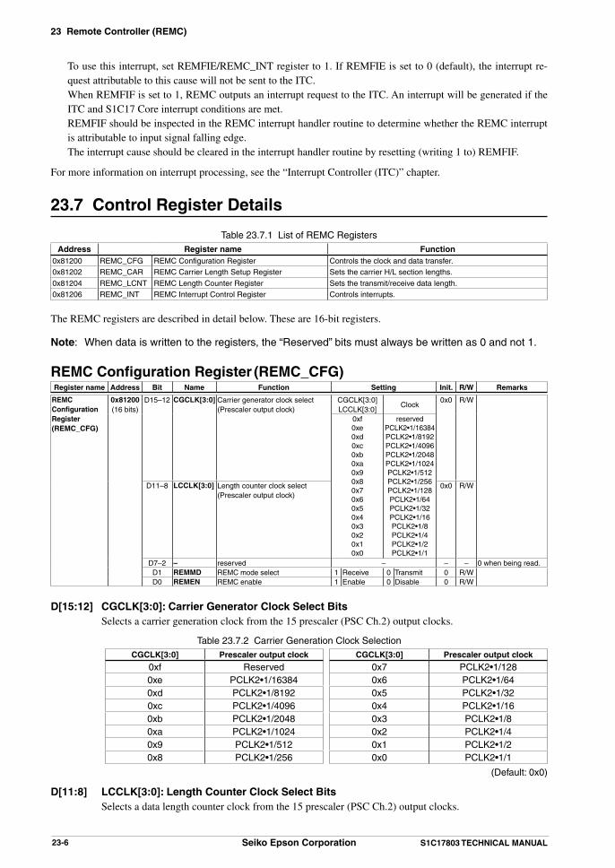
23 Remote Controller (REMC)
23-6 Seiko Epson Corporation S1C17803 TECHNICAL MANUAL
To use this interrupt, set REMFIE/REMC_INT register to 1. If REMFIE is set to 0 (default), the interrupt re-quest attributable to this cause will not be sent to the ITC.
When REMFIF is set to 1, REMC outputs an interrupt request to the ITC. An interrupt will be generated if the ITC and S1C17 Core interrupt conditions are met.
REMFIF should be inspected in the REMC interrupt handler routine to determine whether the REMC interrupt is attributable to input signal falling edge.
The interrupt cause should be cleared in the interrupt handler routine by resetting (writing 1 to) REMFIF.
For more information on interrupt processing, see the “Interrupt Controller (ITC)” chapter.
23.7 Control Register Details
Table 23.7.1 List of REMC RegistersAddress Register name Function
0x81200 REMC_CFG REMC Configuration Register Controls the clock and data transfer.0x81202 REMC_CAR REMC Carrier Length Setup Register Sets the carrier H/L section lengths.
0x81204 REMC_LCNT REMC Length Counter Register Sets the transmit/receive data length.0x81206 REMC_INT REMC Interrupt Control Register Controls interrupts.
The REMC registers are described in detail below. These are 16-bit registers.
Note: When data is written to the registers, the “Reserved” bits must always be written as 0 and not 1.
REMC Configuration Register (REMC_CFG)Register name Address Bit Name Function Setting Init. R/W Remarks
REMC Configuration Register(REMC_CFG)
0x81200(16 bits)
D15–12 CGCLK[3:0] Carrier generator clock select(Prescaler output clock)
CGCLK[3:0]LCCLK[3:0]
Clock0x0 R/W
0xf0xe0xd0xc0xb0xa0x90x80x70x60x50x40x30x20x10x0
reservedPCLK2•1/16384PCLK2•1/8192PCLK2•1/4096PCLK2•1/2048PCLK2•1/1024PCLK2•1/512PCLK2•1/256PCLK2•1/128PCLK2•1/64PCLK2•1/32PCLK2•1/16PCLK2•1/8PCLK2•1/4PCLK2•1/2PCLK2•1/1
D11–8 LCCLK[3:0] Length counter clock select(Prescaler output clock)
0x0 R/W
D7–2 – reserved – – – 0 when being read.D1 REMMD REMC mode select 1 Receive 0 Transmit 0 R/WD0 REMEN REMC enable 1 Enable 0 Disable 0 R/W
D[15:12] CGCLK[3:0]: Carrier Generator Clock Select Bits Selects a carrier generation clock from the 15 prescaler (PSC Ch.2) output clocks.
Table 23.7.2 Carrier Generation Clock SelectionCGCLK[3:0] Prescaler output clock CGCLK[3:0] Prescaler output clock
0xf Reserved 0x7 PCLK2•1/1280xe PCLK2•1/16384 0x6 PCLK2•1/640xd PCLK2•1/8192 0x5 PCLK2•1/320xc PCLK2•1/4096 0x4 PCLK2•1/160xb PCLK2•1/2048 0x3 PCLK2•1/80xa PCLK2•1/1024 0x2 PCLK2•1/40x9 PCLK2•1/512 0x1 PCLK2•1/20x8 PCLK2•1/256 0x0 PCLK2•1/1
(Default: 0x0)
D[11:8] LCCLK[3:0]: Length Counter Clock Select Bits Selects a data length counter clock from the 15 prescaler (PSC Ch.2) output clocks.

23 Remote Controller (REMC)
S1C17803 TECHNICAL MANUAL Seiko Epson Corporation 23-7
Table 23.7.3 Data Length Counter Clock SelectionLCCLK[3:0] Prescaler output clock LCCLK[3:0] Prescaler output clock
0xf Reserved 0x7 PCLK2•1/1280xe PCLK2•1/16384 0x6 PCLK2•1/640xd PCLK2•1/8192 0x5 PCLK2•1/320xc PCLK2•1/4096 0x4 PCLK2•1/160xb PCLK2•1/2048 0x3 PCLK2•1/80xa PCLK2•1/1024 0x2 PCLK2•1/40x9 PCLK2•1/512 0x1 PCLK2•1/20x8 PCLK2•1/256 0x0 PCLK2•1/1
(Default: 0x0)
Note: The clock should be set only while the REMC module is stopped (REMEN = 0).
D[7:2] Reserved
D1 REMMD: REMC Mode Select Bit Selects the transfer direction. 1 (R/W): Reception 0 (R/W): Transmission (default)
D0 REMEN: REMC Enable Bit Enables or disables data transfer by the REMC module. 1 (R/W): Enabled 0 (R/W): Disabled (default)
Setting REMEN to 1 starts transmission or receiving in accordance with REMMD settings. Setting REMEN to 0 disables REMC module operations.
REMC Carrier Length Setup Register (REMC_CAR)Register name Address Bit Name Function Setting Init. R/W Remarks
REMC Carrier Length Setup Register(REMC_CAR)
0x81202(16 bits)
D15–14 – reserved – – – 0 when being read.D13–8 REMCL[5:0] Carrier L length setup 0x0 to 0x3f 0x0 R/WD7–6 – reserved – – – 0 when being read.D5–0 REMCH[5:0] Carrier H length setup 0x0 to 0x3f 0x0 R/W
D[15:14] Reserved
D[13:8] REMCL[5:0]: Carrier L Length Setup BitsSets the carrier signal L section length. (Default: 0x0)Specify a value corresponding to the number of carrier generation clock cycles selected by CGCLK[3:0]/REMC_CFG register + 1. Calculate carrier L section length as follows:
REMCL + 1Carrier L section length = —————— [s] clk_in
REMCL: REMCL[5:0] settingclk_in: Prescaler (PSC Ch.2) output clock frequency
The H section length is specified by REMCH[5:0]. The carrier signal is generated from these settings as shown in Figure 23.7.1.
D[7:6] Reserved
D[5:0] REMCH[5:0]: Carrier H Length Setup BitsSets the carrier signal H section length. (Default: 0x0)Specify a value corresponding to the number of carrier generation clock cycles selected by CGCLK[3:0]/REMC_CFG register + 1. Calculate carrier H section length as follows:
REMCH + 1Carrier H section length = —————— [s] clk_in
REMCH: REMCH[5:0] settingclk_in: Prescaler (PSC Ch.2) output clock frequency
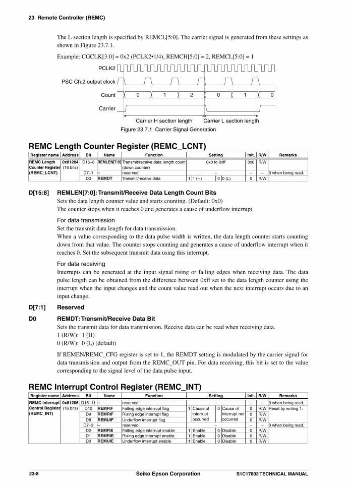
23 Remote Controller (REMC)
23-8 Seiko Epson Corporation S1C17803 TECHNICAL MANUAL
The L section length is specified by REMCL[5:0]. The carrier signal is generated from these settings as shown in Figure 23.7.1.
Example: CGCLK[3:0] = 0x2 (PCLK2•1/4), REMCH[5:0] = 2, REMCL[5:0] = 1
PCLK2
PSC Ch.2 output clock
Count
Carrier
0 1 2 0 1 0
Carrier H section length Carrier L section length
Figure 23.7.1 Carrier Signal Generation
REMC Length Counter Register (REMC_LCNT)Register name Address Bit Name Function Setting Init. R/W Remarks
REMC Length Counter Register(REMC_LCNT)
0x81204(16 bits)
D15–8 REMLEN[7:0] Transmit/receive data length count(down counter)
0x0 to 0xff 0x0 R/W
D7–1 – reserved – – – 0 when being read.D0 REMDT Transmit/receive data 1 1 (H) 0 0 (L) 0 R/W
D[15:8] REMLEN[7:0]: Transmit/Receive Data Length Count Bits Sets the data length counter value and starts counting. (Default: 0x0) The counter stops when it reaches 0 and generates a cause of underflow interrupt.
For data transmission Set the transmit data length for data transmission. When a value corresponding to the data pulse width is written, the data length counter starts counting
down from that value. The counter stops counting and generates a cause of underflow interrupt when it reaches 0. Set the subsequent transmit data using this interrupt.
For data receiving Interrupts can be generated at the input signal rising or falling edges when receiving data. The data
pulse length can be obtained from the difference between 0xff set to the data length counter using the interrupt when the input changes and the count value read out when the next interrupt occurs due to an input change.
D[7:1] Reserved
D0 REMDT: Transmit/Receive Data Bit Sets the transmit data for data transmission. Receive data can be read when receiving data. 1 (R/W): 1 (H) 0 (R/W): 0 (L) (default)
If REMEN/REMC_CFG register is set to 1, the REMDT setting is modulated by the carrier signal for data transmission and output from the REMC_OUT pin. For data receiving, this bit is set to the value corresponding to the signal level of the data pulse input.
REMC Interrupt Control Register (REMC_INT)Register name Address Bit Name Function Setting Init. R/W Remarks
REMC Interrupt Control Register(REMC_INT)
0x81206(16 bits)
D15–11 – reserved – – – 0 when being read.D10 REMFIF Falling edge interrupt flag 1 Cause of
interrupt occurred
0 Cause of interrupt not occurred
0 R/W Reset by writing 1.D9 REMRIF Rising edge interrupt flag 0 R/WD8 REMUIF Underflow interrupt flag 0 R/W
D7–3 – reserved – – – 0 when being read.D2 REMFIE Falling edge interrupt enable 1 Enable 0 Disable 0 R/WD1 REMRIE Rising edge interrupt enable 1 Enable 0 Disable 0 R/WD0 REMUIE Underflow interrupt enable 1 Enable 0 Disable 0 R/W

23 Remote Controller (REMC)
S1C17803 TECHNICAL MANUAL Seiko Epson Corporation 23-9
This register controls the data length counter underflow, input signal rising edge, and input signal falling edge inter-rupts. The interrupt flag is set to 1 when the data length counter underflows, or when an input signal rising edge or falling edge is detected. If the corresponding interrupt enable bit has been set to 1, the REMC outputs an interrupt request signal to the ITC at the same time. An interrupt will be generated if the ITC and S1C17 Core interrupt con-ditions are met. When an REMC interrupt occurs, check the interrupt flag status in this register to identify the cause of interrupt occurred. If the interrupt enable bit is set to 0, the interrupt is disabled.
Notes: • To prevent interrupt recurrences, the REMC module interrupt flag must be reset in the inter-rupt handler routine after an REMC interrupt has occurred.
• To prevent generating unnecessary interrupts, reset the interrupt flag before enabling inter-rupts by the interrupt enable bit.
D[15:11] Reserved
D10 REMFIF: Falling Edge Interrupt Flag Bit Indicates the falling edge interrupt cause occurrence status. 1 (R): Cause of interrupt has occurred 0 (R): No cause of interrupt has occurred (default) 1 (W): Flag is reset 0 (W): Ignored
REMFIF is set to 1 at the input signal falling edge. REMFIF is reset to 0 by writing 1.
D9 REMRIF: Rising Edge Interrupt Flag Bit Indicates the rising edge interrupt cause occurrence status. 1 (R): Cause of interrupt has occurred 0 (R): No cause of interrupt has occurred (default) 1 (W): Flag is reset 0 (W): Ignored
REMRIF is set to 1 at the input signal rising edge. REMRIF is reset to 0 by writing 1.
D8 REMUIF: Underflow Interrupt Flag Bit Indicates the underflow interrupt cause occurrence status. 1 (R): Cause of interrupt has occurred 0 (R): No cause of interrupt has occurred (default) 1 (W): Flag is reset 0 (W): Ignored
REMUIF is set to 1 when a data length counter underflow occurs. REMUIF is reset to 0 by writing 1.
D[7:3] Reserved
D2 REMFIE: Falling Edge Interrupt Enable Bit Enables or disables input signal falling edge interrupts. 1 (R/W): Interrupt enabled 0 (R/W): Interrupt disabled (default)
D1 REMRIE: Rising Edge Interrupt Enable Bit Enables or disables input signal rising edge interrupts. 1 (R/W): Interrupt enabled 0 (R/W): Interrupt disabled (default)
D0 REMUIE: Underflow Interrupt Enable Bit Enables or disables data length counter underflow interrupts. 1 (R/W): Interrupt enabled 0 (R/W): Interrupt disabled (default)

24 Card Interface (CARD)
S1C17803 TECHNICAL MANUAL Seiko Epson Corporation 24-1
24 Card Interface (CARD)
24.1 CARD Module OverviewThe card interface (CARD) module to connect a NAND Flash or SmartMedia cards.The following shows the features of the CARD module:
• Generates the #SMRD and #SMWR signals. (Use general-purpose input/output ports to control the signals specific to NAND Flash or SmartMedia card.)
• Supports 8-bit and 16-bit NAND Flash devices and SmartMedia cards.
• A NAND Flash or SmartMedia cards can be connected to the #CE2 area (0x700000–0xefffff, 8MB).
• The data and address signals of the device can be connected directly to the external bus of the SRAMC.
24.2 CARD Output PinsTable 24.2.1 lists the card interface output pins.
Table 24.2.1 List of Card Interface PinsPin name I/O Qty Function
#SMRD O 1 SmartMedia read signal output pinThis pin outputs the read signal for NAND Flash and SmartMedia card.
#SMWR O 1 SmartMedia write signal output pinThis pin outputs the write signal for NAND Flash and SmartMedia card.
The CARD output pins (#SMRD, #SMWR) are shared with I/O ports and are initially set as general purpose I/O port pins. The pin functions must be switched using the port function select bits to use the general purpose I/O port pins as CARD output pins. For detailed information on pin function switching, see the “I/O Ports (GPIO)” chapter.
24.3 Card Interface Control SignalsFigure 24.3.1 shows the logic used to generate SmartMedia interface signals. Figure 24.3.2 shows an example of connecting the S1C17803 and a SmartMedia card (NAND Flash).
#RD
#CE2
#WR
#SMRD
#SMWR
Figure 24.3.1 SmartMedia Interface Signal Generation Circuit
S1C17803 SmartMedia card(NAND Flash)
D[15:0]or D[7:0]
#CE#RE#WE
CLEALERY/#BY#WP
#CE2#SMRD#SMWR
(Software control) P**
I/O[15:0] (16-bit Flash)or I/O[7:0] (8-bit Flash)
Figure 24.3.2 Example of Connecting a SmartMedia Card

25 I/O Ports (GPIO)
S1C17803 TECHNICAL MANUAL Seiko Epson Corporation 25-1
25 I/O Ports (GPIO)
25.1 GPIO Module OverviewThe S1C17803 includes general-purpose I/O ports that allow software to switch input/output direction. These share internal peripheral module input/output pins, but pins not used for peripheral modules can be used as general-pur-pose I/O ports.The following shows the features of the GPIO module:
• Maximum 93 I/O ports (P1[7:0], P2[7:0], P3[7:0], P4[5:0], P5[7:0], P6[7:0], P7[7:0], P8[6:0], P9[7:0], PA[7:0], PB[7:0], PC[7:0]) and four input ports (P0[3:0]) are available in the 128-pin package model.
Maximum 66 I/O ports (P2[5:0], P3[7:6], P3[3:0], P4[4:0], P5[7:4], P5[2:0], P6[7:0], P7[7:0], P8[4:0], P9[7:0], PA7, PA[5:4], PA2, PA0, PC[7:0]) and three input ports (P0[2:0]) are available in the 100-pin package model.
* The GPIO ports are shared with other peripheral function pins (UART, PWM etc.). Therefore, the number of GPIO ports depends on the peripheral functions used.
• Can generate input interrupts from the ports (P2/P8 and PA/P4) selected with software.
• Interrupt input signal conditions (level or edge trigger, and polarity) can be specified.
• P2/P8 and PA/P4 ports include a chattering filter.
• All port provide a port function select bit to configure the pin function (for GPIO or peripheral functions).
Figure 25.1.1 shows the I/O port configuration.
Peripheral module output
Peripheral I/O controlPxIOy
PxOUTy
CFPxy
I/O direction control
Output data
Function selection
VDD
VSSInte
rnal
dat
a bu
s
Pxy
Peripheral module input
Input dataPxINy
Figure 25.1.1 I/O Port Configuration
Notes: • The PCLK2 clock must be supplied from the CMU to access the I/O port. The prescaler (PSC Ch.2) output clock is also needed to operate the P2/P8 and PA/P4 chattering filters. Turn on the prescaler when using this function.
• The “xy” in the register and bit names refers to the port number (Pxy, x = 0 to C, y = 0 to 7). Example: PxINy/Px_IN register P00: P0IN0/P0_IN register P17: P1IN7/P1_IN register
25.2 Input/Output Pin Function Selection (Port MUX)The I/O port pins share peripheral module input/output pins. Each pin can be configured for use as an I/O port or for a peripheral module function via the corresponding port function select bits. Pins not used for peripheral mod-ules can be used as general-purpose I/O ports.

25 I/O Ports (GPIO)
25-2 Seiko Epson Corporation S1C17803 TECHNICAL MANUAL
Table 25.2.1 Input/Output Pin Function Selection
100pin package
Pin function 1 CFPxx = 0x0
(default)
Pin function 2CFPxx = 0x1
Pin function 3CFPxx = 0x2
Pin function 4CFPxx = 0x3
I/O group(voltage)
Port function select bit
AIN0 P00 Analog (AVDD) CFP00[1:0]/P0_03_CFP registerAIN1 P01 Analog (AVDD) CFP01[1:0]/P0_03_CFP registerAIN2 P02 Analog (AVDD) CFP02[1:0]/P0_03_CFP register
N/A AIN3 P03 Analog (AVDD) CFP03[1:0]/P0_03_CFP registerN/A P10 I2S_SDO IO1 (IO1_VDD) CFP10[1:0]/P1_03_CFP registerN/A P11 I2S_WS IO1 (IO1_VDD) CFP11[1:0]/P1_03_CFP registerN/A P12 I2S_SCK IO1 (IO1_VDD) CFP12[1:0]/P1_03_CFP registerN/A P13 I2S_MCLK IO1 (IO1_VDD) CFP13[1:0]/P1_03_CFP registerN/A P14 CMU_CLK IO1 (IO1_VDD) CFP14[1:0]/P1_47_CFP registerN/A P15 #ADTRG IO1 (IO1_VDD) CFP15[1:0]/P1_47_CFP registerN/A P16 REMC_IN IO1 (IO1_VDD) CFP16[1:0]/P1_47_CFP registerN/A P17 REMC_OUT IO1 (IO1_VDD) CFP17[1:0]/P1_47_CFP register
P20 I2CM_SDA US_SDI0 EXCL0 IO1 (IO1_VDD) CFP20[1:0]/P2_03_CFP registerP21 I2CM_SCL US_SDO0 TMH IO1 (IO1_VDD) CFP21[1:0]/P2_03_CFP registerP22 I2CS_SDA US_SCK0 #SMRD IO1 (IO1_VDD) CFP22[1:0]/P2_03_CFP registerP23 I2CS_SCL #US_SSI0 #SMWR IO1 (IO1_VDD) CFP23[1:0]/P2_03_CFP registerP24 ATMA #ADTRG IO1 (IO1_VDD) CFP24[1:0]/P2_47_CFP registerP25 ATMB #I2CS_BRST IO1 (IO1_VDD) CFP25[1:0]/P2_47_CFP register
N/A P26 #SMRD IO1 (IO1_VDD) CFP26[1:0]/P2_47_CFP registerN/A P27 #SMWR IO1 (IO1_VDD) CFP27[1:0]/P2_47_CFP register
P30 WDT_CLK US_SDI1 EXCL1 IO1 (IO1_VDD) CFP30[1:0]/P3_03_CFP registerP31 SIN US_SDO1 IO1 (IO1_VDD) CFP31[1:0]/P3_03_CFP registerP32 SOUT US_SCK1 IO1 (IO1_VDD) CFP32[1:0]/P3_03_CFP registerP33 #SCLK #US_SSI1 IO1 (IO1_VDD) CFP33[1:0]/P3_03_CFP register
N/A P34 TMH IO1 (IO1_VDD) CFP34[1:0]/P3_47_CFP registerN/A P35 TML IO1 (IO1_VDD) CFP35[1:0]/P3_47_CFP register
DSIO P36 IO1 (IO1_VDD) CFP36[1:0]/P3_47_CFP registerDST2 P37 IO1 (IO1_VDD) CFP37[1:0]/P3_47_CFP registerP40 US_SDI0 I2S_SDO I2CM_SDA IO2 (IO2_VDD) CFP40[1:0]/P4_03_CFP registerP41 US_SDO0 I2S_WS I2CM_SCL IO2 (IO2_VDD) CFP41[1:0]/P4_03_CFP registerP42 US_SCK0 I2S_SCK ATMA IO2 (IO2_VDD) CFP42[1:0]/P4_03_CFP registerP43 #US_SSI0 I2S_MCLK TML IO2 (IO2_VDD) CFP43[1:0]/P4_03_CFP registerP44 EXCL1 TMH I2CS_SDA IO2 (IO2_VDD) CFP44[1:0]/P4_45_CFP register
N/A P45 ATMA TML #I2CS_BRST IO2 (IO2_VDD) CFP45[1:0]/P4_45_CFP registerP50 US_SDI1 CMU_CLK REMC_IN IO2 (IO2_VDD) CFP50[1:0]/P5_03_CFP registerP51 US_SDO1 #WDT_NMI REMC_OUT IO2 (IO2_VDD) CFP51[1:0]/P5_03_CFP registerP52 US_SCK1 WDT_CLK I2CS_SCL IO2 (IO2_VDD) CFP52[1:0]/P5_03_CFP register
N/A P53 #US_SSI1 #ADTRG EXCL0 IO2 (IO2_VDD) CFP53[1:0]/P5_03_CFP registerP54 #SMRD FPFRAME IO2 (IO2_VDD) CFP54[1:0]/P5_47_CFP registerP55 #SMWR FPLINE IO2 (IO2_VDD) CFP55[1:0]/P5_47_CFP registerP56 REMC_IN FPSHIFT IO2 (IO2_VDD) CFP56[1:0]/P5_47_CFP registerP57 REMC_OUT FPDRDY IO2 (IO2_VDD) CFP57[1:0]/P5_47_CFP registerP60 A0/#BSL Bus (BUSIO_VDD) CFP60[1:0]/P6_03_CFP registerP61 A1 Bus (BUSIO_VDD) CFP61[1:0]/P6_03_CFP registerP62 A2 Bus (BUSIO_VDD) CFP62[1:0]/P6_03_CFP registerP63 A3 Bus (BUSIO_VDD) CFP63[1:0]/P6_03_CFP registerP64 A4 Bus (BUSIO_VDD) CFP64[1:0]/P6_47_CFP registerP65 A5 Bus (BUSIO_VDD) CFP65[1:0]/P6_47_CFP registerP66 A6 Bus (BUSIO_VDD) CFP66[1:0]/P6_47_CFP registerP67 A7 Bus (BUSIO_VDD) CFP67[1:0]/P6_47_CFP registerP70 A8 Bus (BUSIO_VDD) CFP70[1:0]/P7_03_CFP registerP71 A9 Bus (BUSIO_VDD) CFP71[1:0]/P7_03_CFP registerP72 A10 Bus (BUSIO_VDD) CFP72[1:0]/P7_03_CFP registerP73 A11 Bus (BUSIO_VDD) CFP73[1:0]/P7_03_CFP registerP74 A12 Bus (BUSIO_VDD) CFP74[1:0]/P7_47_CFP registerP75 A13 Bus (BUSIO_VDD) CFP75[1:0]/P7_47_CFP registerP76 A14 Bus (BUSIO_VDD) CFP76[1:0]/P7_47_CFP registerP77 A15 Bus (BUSIO_VDD) CFP77[1:0]/P7_47_CFP registerP80 A16 Bus (BUSIO_VDD) CFP80[1:0]/P8_03_CFP registerP81 A17 Bus (BUSIO_VDD) CFP81[1:0]/P8_03_CFP registerP82 A18 Bus (BUSIO_VDD) CFP82[1:0]/P8_03_CFP registerP83 A19 Bus (BUSIO_VDD) CFP83[1:0]/P8_03_CFP register

25 I/O Ports (GPIO)
S1C17803 TECHNICAL MANUAL Seiko Epson Corporation 25-3
100pin package
Pin function 1 CFPxx = 0x0
(default)
Pin function 2CFPxx = 0x1
Pin function 3CFPxx = 0x2
Pin function 4CFPxx = 0x3
I/O group(voltage)
Port function select bit
P84 A20 #CE1 Bus (BUSIO_VDD) CFP84[1:0]/P8_46_CFP registerN/A P85 A21 Bus (BUSIO_VDD) CFP85[1:0]/P8_46_CFP registerN/A P86 A22 Bus (BUSIO_VDD) CFP86[1:0]/P8_46_CFP register
P90 D0 Bus (BUSIO_VDD) CFP90[1:0]/P9_03_CFP registerP91 D1 Bus (BUSIO_VDD) CFP91[1:0]/P9_03_CFP registerP92 D2 Bus (BUSIO_VDD) CFP92[1:0]/P9_03_CFP registerP93 D3 Bus (BUSIO_VDD) CFP93[1:0]/P9_03_CFP registerP94 D4 Bus (BUSIO_VDD) CFP94[1:0]/P9_47_CFP registerP95 D5 Bus (BUSIO_VDD) CFP95[1:0]/P9_47_CFP registerP96 D6 Bus (BUSIO_VDD) CFP96[1:0]/P9_47_CFP registerP97 D7 Bus (BUSIO_VDD) CFP97[1:0]/P9_47_CFP registerPA0 #CE0 Bus (BUSIO_VDD) CFPA0[1:0]/PA_03_CFP register
N/A PA1 #CE1 Bus (BUSIO_VDD) CFPA1[1:0]/PA_03_CFP registerPA2 #CE2 Bus (BUSIO_VDD) CFPA2[1:0]/PA_03_CFP register
N/A PA3 #CE3 Bus (BUSIO_VDD) CFPA3[1:0]/PA_03_CFP registerPA4 #RD Bus (BUSIO_VDD) CFPA4[1:0]/PA_47_CFP registerPA5 #WRL Bus (BUSIO_VDD) CFPA5[1:0]/PA_47_CFP register
N/A PA6 #WRH/#BSH Bus (BUSIO_VDD) CFPA6[1:0]/PA_47_CFP registerPA7 #WAIT Bus (BUSIO_VDD) CFPA7[1:0]/PA_47_CFP register
N/A PB0 D8 Bus (BUSIO_VDD) CFPB0[1:0]/PB_03_CFP registerN/A PB1 D9 Bus (BUSIO_VDD) CFPB1[1:0]/PB_03_CFP registerN/A PB2 D10 Bus (BUSIO_VDD) CFPB2[1:0]/PB_03_CFP registerN/A PB3 D11 Bus (BUSIO_VDD) CFPB3[1:0]/PB_03_CFP registerN/A PB4 D12 Bus (BUSIO_VDD) CFPB4[1:0]/PB_47_CFP registerN/A PB5 D13 Bus (BUSIO_VDD) CFPB5[1:0]/PB_47_CFP registerN/A PB6 D14 Bus (BUSIO_VDD) CFPB6[1:0]/PB_47_CFP registerN/A PB7 D15 Bus (BUSIO_VDD) CFPB7[1:0]/PB_47_CFP register
PC0 I2S_SDO FPDAT0 IO2 (IO2_VDD) CFPC0[1:0]/PC_03_CFP registerPC1 I2S_WS FPDAT1 IO2 (IO2_VDD) CFPC1[1:0]/PC_03_CFP registerPC2 I2S_SCK FPDAT2 IO2 (IO2_VDD) CFPC2[1:0]/PC_03_CFP registerPC3 I2S_MCLK FPDAT3 IO2 (IO2_VDD) CFPC3[1:0]/PC_03_CFP registerPC4 TMH FPDAT4 IO2 (IO2_VDD) CFPC4[1:0]/PC_47_CFP registerPC5 TML FPDAT5 IO2 (IO2_VDD) CFPC5[1:0]/PC_47_CFP registerPC6 EXCL0 FPDAT6 IO2 (IO2_VDD) CFPC6[1:0]/PC_47_CFP registerPC7 ATMB FPDAT7 IO2 (IO2_VDD) CFPC7[1:0]/PC_47_CFP register
At initial reset, each I/O port pin (Pxy) is initialized for the default function (“Pin function 1” in Table 25.2.1).
For information on functions other than the I/O ports, see “Pin Descriptions” in the “Overview” chapter or the de-scriptions of peripheral modules. The sections below describe port functions with the pins set as general-purpose I/O ports.
Note: The port function select registers (Px_03_CFP and Px_47_CFP) are write-protected. Before these registers can be rewritten, the write protection must be removed by writing data 0x96 to PFWEN[7:0]/PF_WREN register. Note that since unnecessary rewrites to the port function select registers could lead to erratic system operation, PFWEN[7:0] should be set to other than 0x96 un-less the port function select registers must be rewritten.
25.3 Data Input/Output
Data input/output control The I/O ports allow selection of the data input/output direction for each bit using PxIOy/Px_IO register. Set PxIOy to 0 (default) to configure an I/O port for input; set PxIOy to 1 to configure an I/O port for output.
The input/output direction of ports with a peripheral module function selected is controlled by the peripheral module. PxIOy settings are ignored.

25 I/O Ports (GPIO)
25-4 Seiko Epson Corporation S1C17803 TECHNICAL MANUAL
Data input To input an external signal and read out the value, set PxIOy to 0 (input mode, default). The I/O port is placed
into high-impedance status and it functions as an input port. In input mode, the external signal level can be read out directly from PxINy/Px_IN register. The value read will
be 1 when the input pin is at high level and 0 when it is at low level. The port pin status can also be read in output mode (PxIOy = 1). In this case, the value actually output the port
can be read out from PxINy.
Data output To output data from the port pin, set PxIOy to 1 (output mode). The I/O port then functions as an output port,
and the value set in the PxOUTy/Px_OUT register is output from the port pin. The port pin outputs High level when PxOUTy is set to 1 and Low level when set to 0. Writing to PxOUTy is possible without affecting pin sta-tus, even in input mode.
25.4 Port InterruptThe GPIO module has two interrupt systems (port interrupts 0 and 1) and the ports can be selected for generating each cause of interrupt.The interrupt trigger conditions can also be selected from between input signal edge (rising edge or falling edge) and input signal level (high level or low level).Figure 25.4.1 shows the configuration of the port interrupt circuit.
PIE00
PEDGE0[7:0]
PPOL0[7:0]
PFLAG00
PIE01PFLAG01
PIE02PFLAG02
PIE03PFLAG03
PIE04PFLAG04
PIE05PFLAG05
PIE06PFLAG06
P20P80P21P81P22P82P23P83P24P84P25P85P26P86
P27
P2CHAT0[2:0]PSEL0[6:0]
P2CHAT1[2:0]
Chattering filterfor
P2[7:4]/P8[6:4]
Chattering filterfor
P2[3:0]/P8[3:0]
Trigger mode/polarity
control
PIE07PFLAG07
Port interrupt 0request (to ITC)
Port interrupt 0
PIE10
PEDGE1[7:0]
PPOL1[7:0]
PFLAG10
PIE11PFLAG11
PIE12PFLAG12
PIE13PFLAG13
PIE14PFLAG14
PIE15PFLAG15
PIE16PFLAG16
PA0P40PA1P41PA2P42PA3P43PA4P44PA5P45
PA6
PA7
PACHAT0[2:0]PSEL1[5:0]
PACHAT1[2:0]
Chattering filterfor
PA[7:4]/P4[5:4]
Chattering filterfor
PA[3:0]/P4[3:0]
Trigger mode/polarity
control
PIE17PFLAG17
Port interrupt 1request (to ITC)
Port interrupt 1
Figure 25.4.1 Port Interrupt Circuit Configuration

25 I/O Ports (GPIO)
S1C17803 TECHNICAL MANUAL Seiko Epson Corporation 25-5
Interrupt port selection The port interrupt 0 system uses the eight ports selected from among P2[7:0] and P8[6:0] to generate interrupts.
Select the ports using PSEL0[6:0]/PP_SEL0 register.
Table 25.4.1 Selecting Port Used For Port Interrupt 0
Setting0 1 2 3 4 5 6 7
PSEL00 PSEL01 PSEL02 PSEL03 PSEL04 PSEL05 PSEL06 PSEL070 (default) P20 P21 P22 P23 P24 P25 P26 P27
1 P80 P81 P82 P83 P84 P85 P86 – (P27)
The port interrupt 1 system uses the eight ports selected from among PA[7:0] and P4[5:0] to generate interrupts. Select the ports using PSEL1[5:0]/PP_SEL1 register.
Table 25.4.2 Selecting Port Used For Port Interrupt 1
Setting0 1 2 3 4 5 6 7
PSEL10 PSEL11 PSEL12 PSEL13 PSEL14 PSEL15 PSEL16 PSEL170 (default) PA0 PA1 PA2 PA3 PA4 PA5 PA6 PA7
1 P40 P41 P42 P43 P44 P45 – (PA6) – (PA7)
The P2/P8 and PA/P4 ports include chattering filters that can be enabled/disabled via software. The chattering filter is effective for generating interrupts. See Section 25.5 for the chattering filter.
Trigger mode and polarity selection The GPIO module provides two trigger modes to set the interrupt flags: edge trigger mode and level trigger
mode. The trigger mode for each port can be selected using PEDGE0[7:0]/PP_EDGE0 register for port interrupt 0 and PEDGE1[7:0]/PP_EDGE1 register for port interrupt 1.
When a PEDGE bit is set to 0 (default), the corresponding port is set to edge trigger mode. In edge trigger mode, the interrupt flag is set at the active edge of the input signal and it retains 1 until reset via software.
When a PEDGE bit is set to 1, the corresponding port is set to level trigger mode. In level trigger mode, the in-terrupt flag is set when the input signal goes the active level and it retains 1 until reset via software.
In SLEEP mode, the CMU senses the port interrupt signal level to cancel SLEEP mode. Therefore, the GPIO module sends a level signal to the CMU in SLEEP mode even if edge trigger mode is selected.
The active level/edge of the input signal can be selected using PPOL0[7:0]/PP_POL0 register for port interrupt 0 and PPOL1[7:0]/PP_POL1 register for port interrupt 1.
When a PPOL bit is set to 0 (default), high level (in level trigger mode) or rising edge (in edge trigger mode) is selected.
When a PPOL bit is set to 1, low level (in level trigger mode) or falling edge (in edge trigger mode) is selected.
Table 25.4.3 Port Interrupt ConditionsPEDGE PPOL Port input interrupt condition
1 1 Low level input1 0 High level input0 1 Falling edge input0 0 Rising edge input
Interrupt flags The port interrupt 0 system provides eight interrupt flags (PFLAG0[7:0]/PP_FLAG0 register) corresponding to
the interrupt input ports. The port interrupt 1 system provides eight interrupt flags (PFLAG1[7:0]/PP_FLAG1 register).
In level trigger mode, the interrupt flag is set according to the input signal level. In edge trigger mode, the interrupt flag is set at the active edge of the input signal. In this mode, the interrupt
flag must be reset by writing 1 after an interrupt occurs.
Interrupt enable bits Each port in the port interrupt system can be enabled or disabled to generate interrupts using the corresponding
interrupt enable bit (PIE0[7:0]/PP_IE0 register and PIE1[7:0]/PP_IE1 register). To enable interrupts, set the PIE bit to 1. To disable interrupts, set the PIE bit to 0.

25 I/O Ports (GPIO)
25-6 Seiko Epson Corporation S1C17803 TECHNICAL MANUAL
When a PFLAG bit is set to 1 while the corresponding PIE bit is set to 1, an interrupt request signal is output to the ITC. An interrupt is generated if the ITC and S1C17 Core interrupt conditions are satisfied.
For specific information on interrupt processing, see the “Interrupt Controller (ITC)” chapter.
25.5 Chattering Filters (P2/P8 and PA/P4 Ports)The P2/P8 and PA/P4 ports include a chattering filter circuit for key entry that can be disabled or enabled with a sampling clock specified individually for the four Px[3:0] and Px[7:4] ports using PxCHAT1[2:0]/Px_CHAT regis-ter and PxCHAT2[2:0]/Px_CHAT register, respectively. (x = 2 or A)When the chattering filter is enabled, pulses shorter than the filter time shown in the table below will be filtered as noise.
Table 25.5.1 Chattering Filter SettingsPxCHAT1[2:0]/PxCHAT2[2:0] Filter time
0x7 64/fPCLK2
0x6 32/fPCLK2
0x5 16/fPCLK2
0x4 8/fPCLK2
0x3 4/fPCLK2
0x2 2/fPCLK2
0x1 1/fPCLK2
0x0 Not filtered
(Default: 0x0)
Notes: • The prescaler (PSC Ch.2) output is used as the filter clock. Therefore, The prescaler (PSC Ch.2) must be run to use the chattering filter.
• Input interrupts will not be accepted when the CPU enters SLEEP mode with the chattering filter left on. The chattering filter should be bypassed (Not filtered) before executing the slp in-struction.
• The port interrupt must be disabled before setting the Px_CHAT register. Setting the register while the interrupt is enabled may generate inadvertent port interrupt.
25.6 Input Port Noise FiltersThe S1C17803 provides noise filters to remove noise on the signals input from the ports shown below.
UART: SIN, #SCLKUSI: US_SDI0, US_SDI1, US_SCK0, US_SCK1, #US_SSI0, #US_SSI1SRAMC: #WAITI2CM: I2CM_SDA, I2CM_SCLI2CS: I2CS_SDA, I2CS_SCL, #I2CS_BRSTREMC: REMC_INT16P: EXCL0T16A: EXCL1, ATMA, ATMBADC10: #ADTRG
When using these noise filters, set ANFEN/PP_NFC register to 1. When ANFEN is set to 0 (default), the input sig-nals bypass the noise filters.
Notes: • These noise filters cannot be enabled individually.
• The noise filters are not effective if these ports are used as general-purpose input port.

25 I/O Ports (GPIO)
S1C17803 TECHNICAL MANUAL Seiko Epson Corporation 25-7
25.7 Control Register Details
Table 25.7.1 List of GPIO and Port MUX RegistersAddress Register name Function0x80100 P0_IN P0 Port Input Data Register P0 port input data0x80110 P1_IN P1 Port Input Data Register P1 port input data0x80111 P1_OUT P1 Port Output Data Register P1 port output data0x80112 P1_IO P1 Port I/O Direction Register Controls P1 port input/output directions.0x80120 P2_IN P2 Port Input Data Register P2 port input data0x80121 P2_OUT P2 Port Output Data Register P2 port output data0x80122 P2_IO P2 Port I/O Direction Register Controls P2 port input/output directions.0x80124 PP_EDGE0 Port Interrupt 0 Trigger Mode Select Register Selects the port interrupt 0 trigger mode.0x80125 PP_IE0 Port Interrupt 0 Enable Register Enables port interrupt 0.0x80126 PP_POL0 Port Interrupt 0 Polarity Control Register Selects the signal polarity for generating port interrupt 0.0x80127 PP_FLAG0 Port Interrupt 0 Flag Register Indicates/resets the port interrupt 0 occurrence status.0x80128 P2_CHAT P2 Port Chattering Filter Control Register Controls the P2/P8 port chattering filters.0x80130 P3_IN P3 Port Input Data Register P3 port input data0x80131 P3_OUT P3 Port Output Data Register P3 port output data0x80132 P3_IO P3 Port I/O Direction Register Controls P3 port input/output directions.0x80140 P4_IN P4 Port Input Data Register P4 port input data0x80141 P4_OUT P4 Port Output Data Register P4 port output data0x80142 P4_IO P4 Port I/O Direction Register Controls P4 port input/output directions.0x80145 PP_SEL1 Port Interrupt 1 Port Select Register Selects ports used for port interrupt 1.0x80150 P5_IN P5 Port Input Data Register P5 port input data0x80151 P5_OUT P5 Port Output Data Register P5 port output data0x80152 P5_IO P5 Port I/O Direction Register Controls P5 port input/output directions.0x80160 P6_IN P6 Port Input Data Register P6 port input data0x80161 P6_OUT P6 Port Output Data Register P6 port output data0x80162 P6_IO P6 Port I/O Direction Register Controls P6 port input/output directions.0x80170 P7_IN P7 Port Input Data Register P7 port input data0x80171 P7_OUT P7 Port Output Data Register P7 port output data0x80172 P7_IO P7 Port I/O Direction Register Controls P7 port input/output directions.0x80180 P8_IN P8 Port Input Data Register P8 port input data0x80181 P8_OUT P8 Port Output Data Register P8 port output data0x80182 P8_IO P8 Port I/O Direction Register Controls P8 port input/output directions.0x80185 PP_SEL0 Port Interrupt 0 Port Select Register Selects ports used for port interrupt 0.0x80190 P9_IN P9 Port Input Data Register P9 port input data0x80191 P9_OUT P9 Port Output Data Register P9 port output data0x80192 P9_IO P9 Port I/O Direction Register Controls P9 port input/output directions.0x801a0 PA_IN PA Port Input Data Register PA port input data0x801a1 PA_OUT PA Port Output Data Register PA port output data0x801a2 PA_IO PA Port I/O Direction Register Controls PA port input/output directions.0x801a4 PP_EDGE1 Port Interrupt 1 Trigger Mode Select Register Selects the port interrupt 1 trigger mode.0x801a5 PP_IE1 Port Interrupt 1 Enable Register Enables port interrupt 1.0x801a6 PP_POL1 Port Interrupt 1 Polarity Control Register Selects the signal polarity for generating port interrupt 1.0x801a7 PP_FLAG1 Port Interrupt 1 Flag Register Indicates/resets the port interrupt 1 occurrence status.0x801a8 PA_CHAT PA Port Chattering Filter Control Register Controls the PA/P4 port chattering filters.0x801b0 PB_IN PB Port Input Data Register PB port input data0x801b1 PB_OUT PB Port Output Data Register PB port output data0x801b2 PB_IO PB Port I/O Direction Register Controls PB port input/output directions.0x801c0 PC_IN PC Port Input Data Register PC port input data0x801c1 PC_OUT PC Port Output Data Register PC port output data0x801c2 PC_IO PC Port I/O Direction Register Controls PC port input/output directions.0x80200 P0_03CFP P0[3:0] Port Function Select Register Selects the P0[3:0] port functions.0x80202 P1_03CFP P1[3:0] Port Function Select Register Selects the P1[3:0] port functions.0x80203 P1_47CFP P1[7:4] Port Function Select Register Selects the P1[7:4] port functions.0x80204 P2_03CFP P2[3:0] Port Function Select Register Selects the P2[3:0] port functions.0x80205 P2_47CFP P2[7:4] Port Function Select Register Selects the P2[7:4] port functions.0x80206 P3_03CFP P3[3:0] Port Function Select Register Selects the P3[3:0] port functions.0x80207 P3_47CFP P3[7:4] Port Function Select Register Selects the P3[7:4] port functions.0x80208 P4_03CFP P4[3:0] Port Function Select Register Selects the P4[3:0] port functions.0x80209 P4_45CFP P4[5:4] Port Function Select Register Selects the P4[5:4] port functions.0x8020a P5_03CFP P5[3:0] Port Function Select Register Selects the P5[3:0] port functions.0x8020b P5_47CFP P5[7:4] Port Function Select Register Selects the P5[7:4] port functions.0x8020c P6_03CFP P6[3:0] Port Function Select Register Selects the P6[3:0] port functions.0x8020d P6_47CFP P6[7:4] Port Function Select Register Selects the P6[7:4] port functions.0x8020e P7_03CFP P7[3:0] Port Function Select Register Selects the P7[3:0] port functions.0x8020f P7_47CFP P7[7:4] Port Function Select Register Selects the P7[7:4] port functions.

25 I/O Ports (GPIO)
25-8 Seiko Epson Corporation S1C17803 TECHNICAL MANUAL
Address Register name Function0x80210 P8_03CFP P8[3:0] Port Function Select Register Selects the P8[3:0] port functions.0x80211 P8_46CFP P8[6:4] Port Function Select Register Selects the P8[6:4] port functions.0x80212 P9_03CFP P9[3:0] Port Function Select Register Selects the P9[3:0] port functions.0x80213 P9_47CFP P9[7:4] Port Function Select Register Selects the P9[7:4] port functions.0x80214 PA_03CFP PA[3:0] Port Function Select Register Selects the PA[3:0] port functions.0x80215 PA_47CFP PA[7:4] Port Function Select Register Selects the PA[7:4] port functions.0x80216 PB_03CFP PB[3:0] Port Function Select Register Selects the PB[3:0] port functions.0x80217 PB_47CFP PB[7:4] Port Function Select Register Selects the PB[7:4] port functions.0x80218 PC_03CFP PC[3:0] Port Function Select Register Selects the PC[3:0] port functions.0x80219 PC_47CFP PC[7:4] Port Function Select Register Selects the PC[7:4] port functions.0x8023e PP_NFC P Port Noise Filter Control Register Controls the noise filters for P ports.0x8023f PF_WREN Port Function Protect Register Enables writing to the port function select registers.
The I/O port registers are described in detail below. These are 8-bit registers.
Notes: • When data is written to the registers, the “Reserved” bits must always be written as 0 and not 1.
• The port function select registers (Px_03_CFP and Px_47_CFP) are write-protected. Before these registers can be rewritten, the write protection must be removed by writing data 0x96 to PFWEN[7:0]/PF_WREN register. Note that since unnecessary rewrites to the port function se-lect registers could lead to erratic system operation, PFWEN[7:0] should be set to other than 0x96 unless the port function select registers must be rewritten.
Px Port Input Data Registers (Px_IN)Register name Address Bit Name Function Setting Init. R/W Remarks
Px Port Input Data Register(Px_IN)
0x801000x80110
|0x801c0(8 bits)
D7–0 PxIN[7:0] Px[7:0] port input data 1 1 (H) 0 0 (L) × R
Note: P0IN[3:0], P4IN[5:0], and P8IN[6:0] only are available for P0, P4, and P8 ports, respectively. Other bits are reserved and always read as 0.
D[7:0] PxIN[7:0]: Px[7:0] Port Input Data Bits The port pin status can be read out. (Default: external input status) 1 (R): High level 0 (R): Low level
PxINy corresponds directly to the Pxy pin. The pin voltage level can be read out (even if the port is set to output mode (PxIOy/Px_IO register = 1). The value read out will be 1 when the pin voltage is high and 0 when low. Writing operations to the read-only PxINy is disabled.
Px Port Output Data Registers (Px_OUT)Register name Address Bit Name Function Setting Init. R/W Remarks
Px Port Output Data Register(Px_OUT)
0x801110x80121
|0x801c1(8 bits)
D7–0 PxOUT[7:0] Px[7:0] port output data 1 1 (H) 0 0 (L) 0 R/W
Note: P4OUT[5:0] and P8OUT[6:0] only are available for P4 and P8 ports, respectively. Other bits are reserved and always read as 0. The P0 port does not have an output data register.
D[7:0] PxOUT[7:0]: Px[7:0] Port Output Data Bits Sets the data to be output from the port pin. 1 (R/W): High level 0 (R/W): Low level (default)
PxOUTy corresponds directly to the Pxy pins. The data written will be output unchanged from the port pins when the port is set to output mode (PxIOy/Px_IO register = 1). The port pin will be high when the data bit is set to 1 and low when set to 0.
Port data can also be written in input mode (PxIOy = 0) (the pin status is unaffected).

25 I/O Ports (GPIO)
S1C17803 TECHNICAL MANUAL Seiko Epson Corporation 25-9
Px Port I/O Direction Registers (Px_IO)Register name Address Bit Name Function Setting Init. R/W Remarks
Px Port I/O Direction Register(Px_OEN)
0x801120x80122
|0x801c2(8 bits)
D7–0 PxIO[7:0] Px[7:0] port I/O direction control 1 Output 0 Input 0 R/W
Note: P4IO[5:0] and P8IO[6:0] only are available for P4 and P8 ports, respectively. Other bits are re-served and always read as 0. The P0 port does not have an I/O direction register.
D[7:0] PxIO[7:0]: Px[7:0] Port I/O Direction Control Bits Sets the port to input or output mode. 1 (R/W): Output mode 0 (R/W): Input mode (default)
PxIOy is the I/O direction control bit that corresponds directly to Pxy port. Setting to 1 enables output and the data set in PxOUTy is output from the port pin. Output is disabled when PxIOy is set to 0, and the port pin is set into high-impedance status for inputting an external signal. The peripheral module de-termines whether output is enabled or disabled when the port is used for a peripheral module function.
Port Interrupt 0 Port Select Register (PP_SEL0)Register name Address Bit Name Function Setting Init. R/W Remarks
Port Interrupt 0 Port Select Register(PP_SEL0)
0x80185(8 bits)
D7 PSEL07 Port interrupt 07 port select P27 0 RD6 PSEL06 Port interrupt 06 port select 1 P86 0 P26 0 R/WD5 PSEL05 Port interrupt 05 port select 1 P85 0 P25 0 R/WD4 PSEL04 Port interrupt 04 port select 1 P84 0 P24 0 R/WD3 PSEL03 Port interrupt 03 port select 1 P83 0 P23 0 R/WD2 PSEL02 Port interrupt 02 port select 1 P82 0 P22 0 R/WD1 PSEL01 Port interrupt 01 port select 1 P81 0 P21 0 R/WD0 PSEL00 Port interrupt 00 port select 1 P80 0 P20 0 R/W
D[7:0] PSEL0[7:0]: Port Interrupt 0[7:0] Port Select Bits Selects the ports used for generating port interrupt 0. 1 (R/W): P8y port 0 (R/W): P2y port (default)
PSEL07 is a read only bit that is fixed at 0 (always P27 is selected).
Port Interrupt 1 Port Select Register (PP_SEL1)Register name Address Bit Name Function Setting Init. R/W Remarks
Port Interrupt 1 Port Select Register(PP_SEL1)
0x80145(8 bits)
D7 PSEL17 Port interrupt 17 port select PA7 0 RD6 PSEL16 Port interrupt 16 port select PA6 0 RD5 PSEL15 Port interrupt 15 port select 1 P45 0 PA5 0 R/WD4 PSEL14 Port interrupt 14 port select 1 P44 0 PA4 0 R/WD3 PSEL13 Port interrupt 13 port select 1 P43 0 PA3 0 R/WD2 PSEL12 Port interrupt 12 port select 1 P42 0 PA2 0 R/WD1 PSEL11 Port interrupt 11 port select 1 P41 0 PA1 0 R/WD0 PSEL10 Port interrupt 10 port select 1 P40 0 PA0 0 R/W
D[7:0] PSEL1[7:0]: Port Interrupt 1[7:0] Port Select Bits Selects the ports used for generating port interrupt 1. 1 (R/W): P4y port 0 (R/W): PAy port (default)
PSEL16 and PSEL17 are read only bits that are fixed at 0 (always PA6 and PA7 are selected).

25 I/O Ports (GPIO)
25-10 Seiko Epson Corporation S1C17803 TECHNICAL MANUAL
Port Interrupt 0 Trigger Mode Select Register (PP_EDGE0)Register name Address Bit Name Function Setting Init. R/W Remarks
Port Interrupt 0 Trigger Mode Select Register(PP_EDGE0)
0x80124(8 bits)
D7 PEDGE07 Port int. 07 trigger mode select 1 Level trigger 0 Edge trigger 0 R/WD6 PEDGE06 Port int. 06 trigger mode select 1 Level trigger 0 Edge trigger 0 R/WD5 PEDGE05 Port int. 05 trigger mode select 1 Level trigger 0 Edge trigger 0 R/WD4 PEDGE04 Port int. 04 trigger mode select 1 Level trigger 0 Edge trigger 0 R/WD3 PEDGE03 Port int. 03 trigger mode select 1 Level trigger 0 Edge trigger 0 R/WD2 PEDGE02 Port int. 02 trigger mode select 1 Level trigger 0 Edge trigger 0 R/WD1 PEDGE01 Port int. 01 trigger mode select 1 Level trigger 0 Edge trigger 0 R/WD0 PEDGE00 Port int. 00 trigger mode select 1 Level trigger 0 Edge trigger 0 R/W
D[7:0] PEDGE0[7:0]: Port Interrupt 0[7:0] Trigger Mode Select Bits Selects trigger modes of the ports used for port interrupt 0. 1 (R/W): Level trigger mode 0 (R/W): Edge trigger mode (default)
When a PEDGE bit is set to 0 (default), the corresponding port is set to edge trigger mode. In edge trig-ger mode, the interrupt flag is set at the active edge of the input signal and it retains 1 until reset via software.
When a PEDGE bit is set to 1, the corresponding port is set to level trigger mode. In level trigger mode, the interrupt flag is set when the input signal goes the active level and it retains 1 until reset via soft-ware. In SLEEP mode, the CMU senses the port interrupt signal level to cancel SLEEP mode. There-fore, the GPIO module sends a level signal to the CMU in SLEEP mode even if edge trigger mode is selected.
Port Interrupt 1 Trigger Mode Select Register (PP_EDGE1)Register name Address Bit Name Function Setting Init. R/W Remarks
Port Interrupt 1 Trigger Mode Select Register(PP_EDGE1)
0x801a4(8 bits)
D7 PEDGE17 Port int. 17 trigger mode select 1 Level trigger 0 Edge trigger 0 R/WD6 PEDGE16 Port int. 16 trigger mode select 1 Level trigger 0 Edge trigger 0 R/WD5 PEDGE15 Port int. 15 trigger mode select 1 Level trigger 0 Edge trigger 0 R/WD4 PEDGE14 Port int. 14 trigger mode select 1 Level trigger 0 Edge trigger 0 R/WD3 PEDGE13 Port int. 13 trigger mode select 1 Level trigger 0 Edge trigger 0 R/WD2 PEDGE12 Port int. 12 trigger mode select 1 Level trigger 0 Edge trigger 0 R/WD1 PEDGE11 Port int. 11 trigger mode select 1 Level trigger 0 Edge trigger 0 R/WD0 PEDGE10 Port int. 10 trigger mode select 1 Level trigger 0 Edge trigger 0 R/W
D[7:0] PEDGE1[7:0]: Port Interrupt 1[7:0] Trigger Mode Select Bits Selects trigger modes of the ports used for port interrupt 1. 1 (R/W): Level trigger mode 0 (R/W): Edge trigger mode (default)
See the descriptions of PEDGE0[7:0]/PP_EDGE0 register.
Port Interrupt 0 Enable Register (PP_IE0)Register name Address Bit Name Function Setting Init. R/W Remarks
Port Interrupt 0 Enable Register(PP_IE0)
0x80125(8 bits)
D7 PIE07 Port interrupt 07 enable 1 Enable 0 Disable 0 R/WD6 PIE06 Port interrupt 06 enable 1 Enable 0 Disable 0 R/WD5 PIE05 Port interrupt 05 enable 1 Enable 0 Disable 0 R/WD4 PIE04 Port interrupt 04 enable 1 Enable 0 Disable 0 R/WD3 PIE03 Port interrupt 03 enable 1 Enable 0 Disable 0 R/WD2 PIE02 Port interrupt 02 enable 1 Enable 0 Disable 0 R/WD1 PIE01 Port interrupt 01 enable 1 Enable 0 Disable 0 R/WD0 PIE00 Port interrupt 00 enable 1 Enable 0 Disable 0 R/W
D[7:0] PIE0[7:0]: Port Interrupt 0[7:0] Enable Bits Enables or disables the ports to generate port interrupt 0. 1 (R/W): Interrupt enabled 0 (R/W): Interrupt disabled (default)

25 I/O Ports (GPIO)
S1C17803 TECHNICAL MANUAL Seiko Epson Corporation 25-11
Port Interrupt 1 Enable Register (PP_IE1)Register name Address Bit Name Function Setting Init. R/W Remarks
Port Interrupt 1 Enable Register(PP_IE1)
0x801a5(8 bits)
D7 PIE17 Port interrupt 17 enable 1 Enable 0 Disable 0 R/WD6 PIE16 Port interrupt 16 enable 1 Enable 0 Disable 0 R/WD5 PIE15 Port interrupt 15 enable 1 Enable 0 Disable 0 R/WD4 PIE14 Port interrupt 14 enable 1 Enable 0 Disable 0 R/WD3 PIE13 Port interrupt 13 enable 1 Enable 0 Disable 0 R/WD2 PIE12 Port interrupt 12 enable 1 Enable 0 Disable 0 R/WD1 PIE11 Port interrupt 11 enable 1 Enable 0 Disable 0 R/WD0 PIE10 Port interrupt 10 enable 1 Enable 0 Disable 0 R/W
D[7:0] PIE1[7:0]: Port Interrupt 1[7:0] Enable Bits Enables or disables the ports to generate port interrupt 1. 1 (R/W): Interrupt enabled 0 (R/W): Interrupt disabled (default)
Port Interrupt 0 Polarity Control Register (PP_POL0)Register name Address Bit Name Function Setting Init. R/W Remarks
Port Interrupt 0 Polarity Control Register(PP_POL0)
0x80126(8 bits)
D7 PPOL07 Port int. 07 signal polarity select 1 Low / ↓ 0 High / ↑ 0 R/WD6 PPOL06 Port int. 06 signal polarity select 1 Low / ↓ 0 High / ↑ 0 R/WD5 PPOL05 Port int. 05 signal polarity select 1 Low / ↓ 0 High / ↑ 0 R/WD4 PPOL04 Port int. 04 signal polarity select 1 Low / ↓ 0 High / ↑ 0 R/WD3 PPOL03 Port int. 03 signal polarity select 1 Low / ↓ 0 High / ↑ 0 R/WD2 PPOL02 Port int. 02 signal polarity select 1 Low / ↓ 0 High / ↑ 0 R/WD1 PPOL01 Port int. 01 signal polarity select 1 Low / ↓ 0 High / ↑ 0 R/WD0 PPOL00 Port int. 00 signal polarity select 1 Low / ↓ 0 High / ↑ 0 R/W
D[7:0] PPOL0[7:0]: Port Interrupt 0[7:0] Signal Polarity Select Bits Selects the interrupt trigger level or edge for the ports used for port interrupt 0. 1 (R/W): Low level/Falling edge 0 (R/W): High level/Rising edge (default)
When a PPOL bit is set to 0 (default), high level (in level trigger mode) or rising edge (in edge trigger mode) is selected as the interrupt generating condition of the corresponding port.
When a PPOL bit is set to 1, low level (in level trigger mode) or falling edge (in edge trigger mode) is selected.
Port Interrupt 1 Polarity Control Register (PP_POL1)Register name Address Bit Name Function Setting Init. R/W Remarks
Port Interrupt 1 Polarity Control Register(PP_POL1)
0x801a6(8 bits)
D7 PPOL17 Port int. 17 signal polarity select 1 Low / ↓ 0 High / ↑ 0 R/WD6 PPOL16 Port int. 16 signal polarity select 1 Low / ↓ 0 High / ↑ 0 R/WD5 PPOL15 Port int. 15 signal polarity select 1 Low / ↓ 0 High / ↑ 0 R/WD4 PPOL14 Port int. 14 signal polarity select 1 Low / ↓ 0 High / ↑ 0 R/WD3 PPOL13 Port int. 13 signal polarity select 1 Low / ↓ 0 High / ↑ 0 R/WD2 PPOL12 Port int. 12 signal polarity select 1 Low / ↓ 0 High / ↑ 0 R/WD1 PPOL11 Port int. 11 signal polarity select 1 Low / ↓ 0 High / ↑ 0 R/WD0 PPOL10 Port int. 10 signal polarity select 1 Low / ↓ 0 High / ↑ 0 R/W
D[7:0] PPOL1[7:0]: Port Interrupt 1[7:0] Signal Polarity Select Bits Selects the interrupt trigger level or edge for the ports used for port interrupt 1. 1 (R/W): Low level/Falling edge 0 (R/W): High level/Rising edge (default)
When a PPOL bit is set to 0 (default), high level (in level trigger mode) or rising edge (in edge trigger mode) is selected as the interrupt generating condition of the corresponding port.
When a PPOL bit is set to 1, low level (in level trigger mode) or falling edge (in edge trigger mode) is selected.

25 I/O Ports (GPIO)
25-12 Seiko Epson Corporation S1C17803 TECHNICAL MANUAL
Port Interrupt 0 Flag Register (PP_FLAG0)Register name Address Bit Name Function Setting Init. R/W Remarks
Port Interrupt 0 Flag Register(PP_FLAG0)
0x80127(8 bits)
D7 PFLAG07 Port interrupt 07 flag 1 Cause of interrupt occurred
0 Cause of interrupt not occurred
0 R/W Reset by writing 1 in edge trigger mode.D6 PFLAG06 Port interrupt 06 flag 0 R/W
D5 PFLAG05 Port interrupt 05 flag 0 R/WD4 PFLAG04 Port interrupt 04 flag 0 R/WD3 PFLAG03 Port interrupt 03 flag 0 R/WD2 PFLAG02 Port interrupt 02 flag 0 R/WD1 PFLAG01 Port interrupt 01 flag 0 R/WD0 PFLAG00 Port interrupt 00 flag 0 R/W
D[7:0] PFLAG0[7:0]: Port Interrupt 0[7:0] Flag Bits These are interrupt flags indicating the interrupt cause occurrence status. 1 (R): Interrupt cause occurred 0 (R): No interrupt cause occurred (default) 1 (W): Reset flag 0 (W): Ignored
PFLAG is the interrupt flag corresponding to the individual ports for port interrupts and is set to 1 at the specified edge (rising or falling edge) or level (high or low) of the input signal. When the corresponding PIE bit has been set to 1, a port interrupt 0 request signal is also output to the ITC at the same time. An interrupt is generated if the ITC and S1C17 Core interrupt conditions are satisfied.
In edge trigger mode, the PFLAG bit is reset by writing 1. In level trigger mode, the PFLAG bit is reset by writing 1.
Port Interrupt 1 Flag Register (PP_FLAG1)Register name Address Bit Name Function Setting Init. R/W Remarks
Port Interrupt 1 Flag Register(PP_FLAG1)
0x801a7(8 bits)
D7 PFLAG17 Port interrupt 17 flag 1 Cause of interrupt occurred
0 Cause of interrupt not occurred
0 R/W Reset by writing 1 in edge trigger mode.D6 PFLAG16 Port interrupt 16 flag 0 R/W
D5 PFLAG15 Port interrupt 15 flag 0 R/WD4 PFLAG14 Port interrupt 14 flag 0 R/WD3 PFLAG13 Port interrupt 13 flag 0 R/WD2 PFLAG12 Port interrupt 12 flag 0 R/WD1 PFLAG11 Port interrupt 11 flag 0 R/WD0 PFLAG10 Port interrupt 10 flag 0 R/W
D[7:0] PFLAG1[7:0]: Port Interrupt 1[7:0] Flag Bits These are interrupt flags indicating the interrupt cause occurrence status. 1 (R): Interrupt cause occurred 0 (R): No interrupt cause occurred (default) 1 (W): Reset flag 0 (W): Ignored
PFLAG is the interrupt flag corresponding to the individual ports for port interrupts and is set to 1 at the specified edge (rising or falling edge) or level (high or low) of the input signal. When the corresponding PIE bit has been set to 1, a port interrupt 1 request signal is also output to the ITC at the same time. An interrupt is generated if the ITC and S1C17 Core interrupt conditions are satisfied.
In edge trigger mode, the PFLAG bit is reset by writing 1. In level trigger mode, the PFLAG bit is reset by writing 1.

25 I/O Ports (GPIO)
S1C17803 TECHNICAL MANUAL Seiko Epson Corporation 25-13
P2 Port Chattering Filter Control Register (P2_CHAT)Register name Address Bit Name Function Setting Init. R/W Remarks
P2 Port Chattering Filter Control Register(P2_CHAT)
0x80128(8 bits)
D7 – reserved – – – 0 when being read.D6–4 P2CHAT1
[2:0]P2[7:4]/P8[6:4] chattering filter time select
P2CHAT1[2:0] Filter time 0x0 R/W0x70x60x50x40x30x20x10x0
64/fPCLK2
32/fPCLK2
16/fPCLK2
8/fPCLK2
4/fPCLK2
2/fPCLK2
1/fPCLK2
NoneD3 – reserved – – – 0 when being read.
D2–0 P2CHAT0[2:0]
P2[3:0]/P8[3:0] chattering filter time select
P2CHAT0[2:0] Filter time 0x0 R/W0x70x60x50x40x30x20x10x0
64/fPCLK2
32/fPCLK2
16/fPCLK2
8/fPCLK2
4/fPCLK2
2/fPCLK2
1/fPCLK2
None
D7 Reserved
D[6:4] P2CHAT1[2:0]: P2[7:4]/P8[6:4] Chattering Filter Time Select Bits Configures the chattering filter circuit for the P2[7:4]/P8[6:4] ports.
D3 Reserved
D[2:0] P2CHAT0[2:0]: P2[3:0]/P8[3:0] Chattering Filter Time Select Bits Configures the chattering filter circuit for the P2[3:0]/P8[3:0] ports.
The P2 and P8 (PA and P4) ports include a chattering filter circuit for key entry that can be disabled or enabled with a filter time specified individually for the four P2[3:0]/P8[3:0] (PA[3:0]/P4[3:0]) and P2[7:4]/P8[6:4] (PA[7:4]/P4[5:4]) ports using P2CHAT0[2:0] (PACHAT0[2:0]) and P2CHAT1[2:0] (PACHAT1[2:0]), respectively.
Table 25.7.2 Chattering Filter SettingsPxCHAT1[2:0]/PxCHAT0[2:0] Filter time
0x7 64/fPCLK2
0x6 32/fPCLK2
0x5 16/fPCLK2
0x4 8/fPCLK2
0x3 4/fPCLK2
0x2 2/fPCLK2
0x1 1/fPCLK2
0x0 Not filtered
(Default: 0x0)
Notes: • The prescaler (PSC Ch.2) output is used as the filter clock. Therefore, The prescaler (PSC Ch.2) must be run to use the chattering filter.
• Input interrupts will not be accepted when the CPU enters SLEEP mode with the chattering filter left on. The chattering filter should be bypassed (Not filtered) before executing the slp instruction.
• The port interrupt must be disabled before setting the Px_CHAT register. Setting the register while the interrupt is enabled may generate inadvertent port interrupt.

25 I/O Ports (GPIO)
25-14 Seiko Epson Corporation S1C17803 TECHNICAL MANUAL
PA Port Chattering Filter Control Register (PA_CHAT)Register name Address Bit Name Function Setting Init. R/W Remarks
PA Port Chattering Filter Control Register(PA_CHAT)
0x801a8(8 bits)
D7 – reserved – – – 0 when being read.D6–4 PACHAT1
[2:0]PA[7:4]/P4[5:4] chattering filter time select
PACHAT1[2:0] Filter time 0x0 R/W0x70x60x50x40x30x20x10x0
64/fPCLK2
32/fPCLK2
16/fPCLK2
8/fPCLK2
4/fPCLK2
2/fPCLK2
1/fPCLK2
NoneD3 – reserved – – – 0 when being read.
D2–0 PACHAT0[2:0]
PA[3:0]/P4[3:0] chattering filter time select
PACHAT0[2:0] Filter time 0x0 R/W0x70x60x50x40x30x20x10x0
64/fPCLK2
32/fPCLK2
16/fPCLK2
8/fPCLK2
4/fPCLK2
2/fPCLK2
1/fPCLK2
None
D7 Reserved
D[6:4] PACHAT1[2:0]: PA[7:4]/P4[5:4] Chattering Filter Time Select Bits Configures the chattering filter circuit for the PA[7:4]/P4[5:4] ports.
D3 Reserved
D[2:0] PACHAT0[2:0]: PA[3:0]/P4[3:0] Chattering Filter Time Select Bits Configures the chattering filter circuit for the PA[3:0]/P4[3:0] ports.
See the descriptions of P2CHAT0[2:0]/P2_CHAT register.
P0[3:0] Port Function Select Register (P0_03_CFP)Register name Address Bit Name Function Setting Init. R/W Remarks
P0[3:0] Port Function Select Register(P0_03_CFP)
0x80200(8 bits)
D7–6 CFP03[1:0] P03 port function select CFP03[1:0] Function 0x0 R/W Write-protected0x30x20x10x0
reservedreserved
P03AIN3
D5–4 CFP02[1:0] P02 port function select CFP02[1:0] Function 0x0 R/W0x30x20x10x0
reservedreserved
P02AIN2
D3–2 CFP01[1:0] P01 port function select CFP01[1:0] Function 0x0 R/W0x30x20x10x0
reservedreserved
P01AIN1
D1–0 CFP00[1:0] P00 port function select CFP00[1:0] Function 0x0 R/W0x30x20x10x0
reservedreserved
P00AIN0
The GPIO pins are shared with the peripheral module pins. This register is used to select how the pins are used.
D[7:6] CFP03[1:0]: P03 Port Function Select Bits 0x3 (R/W): Reserved 0x2 (R/W): Reserved 0x1 (R/W): P03 port (GPIO) 0x0 (R/W): AIN3 (ADC) (default)
D[5:4] CFP02[1:0]: P02 Port Function Select Bits 0x3 (R/W): Reserved 0x2 (R/W): Reserved 0x1 (R/W): P02 port (GPIO) 0x0 (R/W): AIN2 (ADC) (default)

25 I/O Ports (GPIO)
S1C17803 TECHNICAL MANUAL Seiko Epson Corporation 25-15
D[3:2] CFP01[1:0]: P01 Port Function Select Bits 0x3 (R/W): Reserved 0x2 (R/W): Reserved 0x1 (R/W): P01 port (GPIO) 0x0 (R/W): AIN1 (ADC) (default)
D[1:0] CFP00[1:0]: P00 Port Function Select Bits 0x3 (R/W): Reserved 0x2 (R/W): Reserved 0x1 (R/W): P00 port (GPIO) 0x0 (R/W): AIN0 (ADC) (default)
P1[3:0] Port Function Select Register (P1_03_CFP)Register name Address Bit Name Function Setting Init. R/W Remarks
P1[3:0] Port Function Select Register(P1_03_CFP)
0x80202(8 bits)
D7–6 CFP13[1:0] P13 port function select CFP13[1:0] Function 0x0 R/W Write-protected0x30x20x10x0
reservedreserved
I2S_MCLKP13
D5–4 CFP12[1:0] P12 port function select CFP12[1:0] Function 0x0 R/W0x30x20x10x0
reservedreservedI2S_SCK
P12D3–2 CFP11[1:0] P11 port function select CFP11[1:0] Function 0x0 R/W
0x30x20x10x0
reservedreservedI2S_WS
P11D1–0 CFP10[1:0] P10 port function select CFP10[1:0] Function 0x0 R/W
0x30x20x10x0
reservedreservedI2S_SDO
P10
The GPIO pins are shared with the peripheral module pins. This register is used to select how the pins are used.
D[7:6] CFP13[1:0]: P13 Port Function Select Bits 0x3 (R/W): Reserved 0x2 (R/W): Reserved 0x1 (R/W): I2S_MCLK (I2S) 0x0 (R/W): P13 port (GPIO) (default)
D[5:4] CFP12[1:0]: P12 Port Function Select Bits 0x3 (R/W): Reserved 0x2 (R/W): Reserved 0x1 (R/W): I2S_SCK (I2S) 0x0 (R/W): P12 port (GPIO) (default)
D[3:2] CFP11[1:0]: P11 Port Function Select Bits 0x3 (R/W): Reserved 0x2 (R/W): Reserved 0x1 (R/W): I2S_WS (I2S) 0x0 (R/W): P11 port (GPIO) (default)
D[1:0] CFP10[1:0]: P10 Port Function Select Bits 0x3 (R/W): Reserved 0x2 (R/W): Reserved 0x1 (R/W): I2S_SDO (I2S) 0x0 (R/W): P10 port (GPIO) (default)

25 I/O Ports (GPIO)
25-16 Seiko Epson Corporation S1C17803 TECHNICAL MANUAL
P1[7:4] Port Function Select Register (P1_47_CFP)Register name Address Bit Name Function Setting Init. R/W Remarks
P1[7:4] Port Function Select Register(P1_47_CFP)
0x80203(8 bits)
D7–6 CFP17[1:0] P17 port function select CFP17[1:0] Function 0x0 R/W Write-protected0x30x20x10x0
reservedreserved
REMC_OUTP17
D5–4 CFP16[1:0] P16 port function select CFP16[1:0] Function 0x0 R/W0x30x20x10x0
reservedreserved
REMC_INP16
D3–2 CFP15[1:0] P15 port function select CFP15[1:0] Function 0x0 R/W0x30x20x10x0
reservedreserved#ADTRG
P15D1–0 CFP14[1:0] P14 port function select CFP14[1:0] Function 0x0 R/W
0x30x20x10x0
reservedreserved
CMU_CLKP14
The GPIO pins are shared with the peripheral module pins. This register is used to select how the pins are used.
D[7:6] CFP17[1:0]: P17 Port Function Select Bits 0x3 (R/W): Reserved 0x2 (R/W): Reserved 0x1 (R/W): REMC_OUT (REMC) 0x0 (R/W): P17 port (GPIO) (default)
D[5:4] CFP16[1:0]: P16 Port Function Select Bits 0x3 (R/W): Reserved 0x2 (R/W): Reserved 0x1 (R/W): REMC_IN (REMC) 0x0 (R/W): P16 port (GPIO) (default)
D[3:2] CFP15[1:0]: P15 Port Function Select Bits 0x3 (R/W): Reserved 0x2 (R/W): Reserved 0x1 (R/W): #ADTRG (ADC) 0x0 (R/W): P15 port (GPIO) (default)
D[1:0] CFP14[1:0]: P14 Port Function Select Bits 0x3 (R/W): Reserved 0x2 (R/W): Reserved 0x1 (R/W): CMU_CLK (CMU) 0x0 (R/W): P14 port (GPIO) (default)

25 I/O Ports (GPIO)
S1C17803 TECHNICAL MANUAL Seiko Epson Corporation 25-17
P2[3:0] Port Function Select Register (P2_03_CFP)Register name Address Bit Name Function Setting Init. R/W Remarks
P2[3:0] Port Function Select Register(P2_03_CFP)
0x80204(8 bits)
D7–6 CFP23[1:0] P23 port function select CFP23[1:0] Function 0x0 R/W Write-protected0x30x20x10x0
#SMWR#US_SSI0I2CS_SCL
P23D5–4 CFP22[1:0] P22 port function select CFP22[1:0] Function 0x0 R/W
0x30x20x10x0
#SMRDUS_SCK0I2CS_SDA
P22D3–2 CFP21[1:0] P21 port function select CFP21[1:0] Function 0x0 R/W
0x30x20x10x0
TMHUS_SDO0I2CM_SCL
P21D1–0 CFP20[1:0] P20 port function select CFP20[1:0] Function 0x0 R/W
0x30x20x10x0
EXCL0US_SDI0
I2CM_SDAP20
The GPIO pins are shared with the peripheral module pins. This register is used to select how the pins are used.
D[7:6] CFP23[1:0]: P23 Port Function Select Bits 0x3 (R/W): #SMWR (CARD) 0x2 (R/W): #US_SSI0 (USI Ch.0) 0x1 (R/W): I2CS_SCL (I2CS) 0x0 (R/W): P23 port (GPIO) (default)
D[5:4] CFP22[1:0]: P22 Port Function Select Bits 0x3 (R/W): #SMRD (CARD) 0x2 (R/W): US_SCK0 (USI Ch.0) 0x1 (R/W): I2CS_SDA (I2CS) 0x0 (R/W): P22 port (GPIO) (default)
D[3:2] CFP21[1:0]: P21 Port Function Select Bits 0x3 (R/W): TMH (T16P) 0x2 (R/W): US_SDO0 (USI Ch.0) 0x1 (R/W): I2CM_SCL (I2CM) 0x0 (R/W): P21 port (GPIO) (default)
D[1:0] CFP20[1:0]: P20 Port Function Select Bits 0x3 (R/W): EXCL0 (T16P) 0x2 (R/W): US_SDI0 (USI Ch.0) 0x1 (R/W): I2CM_SDA (I2CM) 0x0 (R/W): P20 port (GPIO) (default)

25 I/O Ports (GPIO)
25-18 Seiko Epson Corporation S1C17803 TECHNICAL MANUAL
P2[7:4] Port Function Select Register (P2_47_CFP)Register name Address Bit Name Function Setting Init. R/W Remarks
P2[7:4] Port Function Select Register(P2_47_CFP)
0x80205(8 bits)
D7–6 CFP27[1:0] P27 port function select CFP27[1:0] Function 0x0 R/W Write-protected0x30x20x10x0
reservedreserved#SMWR
P27D5–4 CFP26[1:0] P26 port function select CFP26[1:0] Function 0x0 R/W
0x30x20x10x0
reservedreserved#SMRD
P26D3–2 CFP25[1:0] P25 port function select CFP25[1:0] Function 0x0 R/W
0x30x20x10x0
reserved#I2CS_BRST
ATMBP25
D1–0 CFP24[1:0] P24 port function select CFP24[1:0] Function 0x0 R/W0x30x20x10x0
reserved#ADTRG
ATMAP24
The GPIO pins are shared with the peripheral module pins. This register is used to select how the pins are used.
D[7:6] CFP27[1:0]: P27 Port Function Select Bits 0x3 (R/W): Reserved 0x2 (R/W): Reserved 0x1 (R/W): #SMWR (CARD) 0x0 (R/W): P27 port (GPIO) (default)
D[5:4] CFP26[1:0]: P26 Port Function Select Bits 0x3 (R/W): Reserved 0x2 (R/W): Reserved 0x1 (R/W): #SMRD (CARD) 0x0 (R/W): P26 port (GPIO) (default)
D[3:2] CFP25[1:0]: P25 Port Function Select Bits 0x3 (R/W): Reserved 0x2 (R/W): #I2CS_BRST (I2CS) 0x1 (R/W): ATMB (T16A) 0x0 (R/W): P25 port (GPIO) (default)
D[1:0] CFP24[1:0]: P24 Port Function Select Bits 0x3 (R/W): Reserved 0x2 (R/W): #ADTRG (ADC) 0x1 (R/W): ATMA (T16A) 0x0 (R/W): P24 port (GPIO) (default)
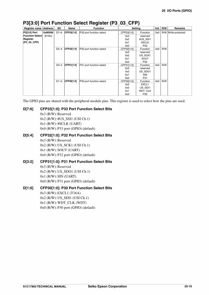
25 I/O Ports (GPIO)
S1C17803 TECHNICAL MANUAL Seiko Epson Corporation 25-19
P3[3:0] Port Function Select Register (P3_03_CFP)Register name Address Bit Name Function Setting Init. R/W Remarks
P3[3:0] Port Function Select Register(P3_03_CFP)
0x80206(8 bits)
D7–6 CFP33[1:0] P33 port function select CFP33[1:0] Function 0x0 R/W Write-protected0x30x20x10x0
reserved#US_SSI1
#SCLKP33
D5–4 CFP32[1:0] P32 port function select CFP32[1:0] Function 0x0 R/W0x30x20x10x0
reservedUS_SCK1
SOUTP32
D3–2 CFP31[1:0] P31 port function select CFP31[1:0] Function 0x0 R/W0x30x20x10x0
reservedUS_SDO1
SINP31
D1–0 CFP30[1:0] P30 port function select CFP30[1:0] Function 0x0 R/W0x30x20x10x0
EXCL1US_SDI1
WDT_CLKP30
The GPIO pins are shared with the peripheral module pins. This register is used to select how the pins are used.
D[7:6] CFP33[1:0]: P33 Port Function Select Bits 0x3 (R/W): Reserved 0x2 (R/W): #US_SSI1 (USI Ch.1) 0x1 (R/W): #SCLK (UART) 0x0 (R/W): P33 port (GPIO) (default)
D[5:4] CFP32[1:0]: P32 Port Function Select Bits 0x3 (R/W): Reserved 0x2 (R/W): US_SCK1 (USI Ch.1) 0x1 (R/W): SOUT (UART) 0x0 (R/W): P32 port (GPIO) (default)
D[3:2] CFP31[1:0]: P31 Port Function Select Bits 0x3 (R/W): Reserved 0x2 (R/W): US_SDO1 (USI Ch.1) 0x1 (R/W): SIN (UART) 0x0 (R/W): P31 port (GPIO) (default)
D[1:0] CFP30[1:0]: P30 Port Function Select Bits 0x3 (R/W): EXCL1 (T16A) 0x2 (R/W): US_SDI1 (USI Ch.1) 0x1 (R/W): WDT_CLK (WDT) 0x0 (R/W): P30 port (GPIO) (default)

25 I/O Ports (GPIO)
25-20 Seiko Epson Corporation S1C17803 TECHNICAL MANUAL
P3[7:4] Port Function Select Register (P3_47_CFP)Register name Address Bit Name Function Setting Init. R/W Remarks
P3[7:4] Port Function Select Register(P3_47_CFP)
0x80207(8 bits)
D7–6 CFP37[1:0] P37 port function select CFP37[1:0] Function 0x0 R/W Write-protected0x30x20x10x0
reservedreserved
P37DST2
D5–4 CFP36[1:0] P36 port function select CFP36[1:0] Function 0x0 R/W0x30x20x10x0
reservedreserved
P36DSIO
D3–2 CFP35[1:0] P35 port function select CFP35[1:0] Function 0x0 R/W0x30x20x10x0
reservedreserved
TMLP35
D1–0 CFP34[1:0] P34 port function select CFP34[1:0] Function 0x0 R/W0x30x20x10x0
reservedreserved
TMHP34
The GPIO pins are shared with the peripheral module pins. This register is used to select how the pins are used.
D[7:6] CFP37[1:0]: P37 Port Function Select Bits 0x3 (R/W): Reserved 0x2 (R/W): Reserved 0x1 (R/W): P37 port (GPIO) 0x0 (R/W): DST2 (DBG) (default)
D[5:4] CFP36[1:0]: P36 Port Function Select Bits 0x3 (R/W): Reserved 0x2 (R/W): Reserved 0x1 (R/W): P36 port (GPIO) 0x0 (R/W): DSIO (DBG) (default)
D[3:2] CFP35[1:0]: P35 Port Function Select Bits 0x3 (R/W): Reserved 0x2 (R/W): Reserved 0x1 (R/W): TML (T16P) 0x0 (R/W): P35 port (GPIO) (default)
D[1:0] CFP34[1:0]: P34 Port Function Select Bits 0x3 (R/W): Reserved 0x2 (R/W): Reserved 0x1 (R/W): TMH (T16P) 0x0 (R/W): P34 port (GPIO) (default)

25 I/O Ports (GPIO)
S1C17803 TECHNICAL MANUAL Seiko Epson Corporation 25-21
P4[3:0] Port Function Select Register (P4_03_CFP)Register name Address Bit Name Function Setting Init. R/W Remarks
P4[3:0] Port Function Select Register(P4_03_CFP)
0x80208(8 bits)
D7–6 CFP43[1:0] P43 port function select CFP43[1:0] Function 0x0 R/W Write-protected0x30x20x10x0
TMLI2S_MCLK#US_SSI0
P43D5–4 CFP42[1:0] P42 port function select CFP42[1:0] Function 0x0 R/W
0x30x20x10x0
ATMAI2S_SCKUS_SCK0
P42D3–2 CFP41[1:0] P41 port function select CFP41[1:0] Function 0x0 R/W
0x30x20x10x0
I2CM_SCLI2S_WS
US_SDO0P41
D1–0 CFP40[1:0] P40 port function select CFP40[1:0] Function 0x0 R/W0x30x20x10x0
I2CM_SDAI2S_SDOUS_SDI0
P40
The GPIO pins are shared with the peripheral module pins. This register is used to select how the pins are used.
D[7:6] CFP43[1:0]: P43 Port Function Select Bits 0x3 (R/W): TML (T16P) 0x2 (R/W): I2S_MCLK (I2S) 0x1 (R/W): #US_SSI0 (USI Ch.0) 0x0 (R/W): P43 port (GPIO) (default)
D[5:4] CFP42[1:0]: P42 Port Function Select Bits 0x3 (R/W): ATMA (T16A) 0x2 (R/W): I2S_SCK (I2S) 0x1 (R/W): US_SCK0 (USI Ch.0) 0x0 (R/W): P42 port (GPIO) (default)
D[3:2] CFP41[1:0]: P41 Port Function Select Bits 0x3 (R/W): I2CM_SCL (I2CM) 0x2 (R/W): I2S_WS (I2S) 0x1 (R/W): US_SDO0 (USI Ch.0) 0x0 (R/W): P41 port (GPIO) (default)
D[1:0] CFP40[1:0]: P40 Port Function Select Bits 0x3 (R/W): I2CM_SDA (I2CM) 0x2 (R/W): I2S_SDO (I2S) 0x1 (R/W): US_SDI0 (USI Ch.0) 0x0 (R/W): P40 port (GPIO) (default)
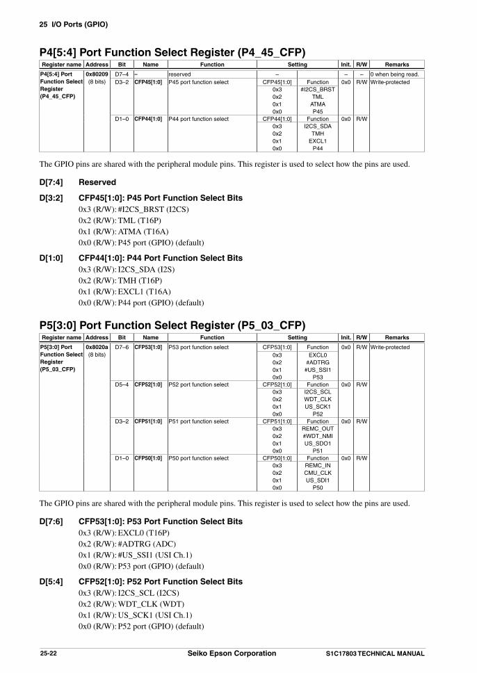
25 I/O Ports (GPIO)
25-22 Seiko Epson Corporation S1C17803 TECHNICAL MANUAL
P4[5:4] Port Function Select Register (P4_45_CFP)Register name Address Bit Name Function Setting Init. R/W Remarks
P4[5:4] Port Function Select Register(P4_45_CFP)
0x80209(8 bits)
D7–4 – reserved – – – 0 when being read.D3–2 CFP45[1:0] P45 port function select CFP45[1:0] Function 0x0 R/W Write-protected
0x30x20x10x0
#I2CS_BRSTTML
ATMAP45
D1–0 CFP44[1:0] P44 port function select CFP44[1:0] Function 0x0 R/W0x30x20x10x0
I2CS_SDATMH
EXCL1P44
The GPIO pins are shared with the peripheral module pins. This register is used to select how the pins are used.
D[7:4] Reserved
D[3:2] CFP45[1:0]: P45 Port Function Select Bits 0x3 (R/W): #I2CS_BRST (I2CS) 0x2 (R/W): TML (T16P) 0x1 (R/W): ATMA (T16A) 0x0 (R/W): P45 port (GPIO) (default)
D[1:0] CFP44[1:0]: P44 Port Function Select Bits 0x3 (R/W): I2CS_SDA (I2S) 0x2 (R/W): TMH (T16P) 0x1 (R/W): EXCL1 (T16A) 0x0 (R/W): P44 port (GPIO) (default)
P5[3:0] Port Function Select Register (P5_03_CFP)Register name Address Bit Name Function Setting Init. R/W Remarks
P5[3:0] Port Function Select Register(P5_03_CFP)
0x8020a(8 bits)
D7–6 CFP53[1:0] P53 port function select CFP53[1:0] Function 0x0 R/W Write-protected0x30x20x10x0
EXCL0#ADTRG
#US_SSI1P53
D5–4 CFP52[1:0] P52 port function select CFP52[1:0] Function 0x0 R/W0x30x20x10x0
I2CS_SCLWDT_CLKUS_SCK1
P52D3–2 CFP51[1:0] P51 port function select CFP51[1:0] Function 0x0 R/W
0x30x20x10x0
REMC_OUT#WDT_NMIUS_SDO1
P51D1–0 CFP50[1:0] P50 port function select CFP50[1:0] Function 0x0 R/W
0x30x20x10x0
REMC_INCMU_CLKUS_SDI1
P50
The GPIO pins are shared with the peripheral module pins. This register is used to select how the pins are used.
D[7:6] CFP53[1:0]: P53 Port Function Select Bits 0x3 (R/W): EXCL0 (T16P) 0x2 (R/W): #ADTRG (ADC) 0x1 (R/W): #US_SSI1 (USI Ch.1) 0x0 (R/W): P53 port (GPIO) (default)
D[5:4] CFP52[1:0]: P52 Port Function Select Bits 0x3 (R/W): I2CS_SCL (I2CS) 0x2 (R/W): WDT_CLK (WDT) 0x1 (R/W): US_SCK1 (USI Ch.1) 0x0 (R/W): P52 port (GPIO) (default)

25 I/O Ports (GPIO)
S1C17803 TECHNICAL MANUAL Seiko Epson Corporation 25-23
D[3:2] CFP51[1:0]: P51 Port Function Select Bits 0x3 (R/W): REMC_OUT (REMC) 0x2 (R/W): #WDT_NMI (WDT) 0x1 (R/W): US_SDO1 (USI Ch.1) 0x0 (R/W): P51 port (GPIO) (default)
D[1:0] CFP50[1:0]: P50 Port Function Select Bits 0x3 (R/W): REMC_IN (REMC) 0x2 (R/W): CMU_CLK (CMU) 0x1 (R/W): US_SDI1 (USI Ch.1) 0x0 (R/W): P50 port (GPIO) (default)
P5[7:4] Port Function Select Register (P5_47_CFP)Register name Address Bit Name Function Setting Init. R/W Remarks
P5[7:4] Port Function Select Register(P5_47_CFP)
0x8020b(8 bits)
D7–6 CFP57[1:0] P57 port function select CFP57[1:0] Function 0x0 R/W Write-protected0x30x20x10x0
reservedFPDRDY
REMC_OUTP57
D5–4 CFP56[1:0] P56 port function select CFP56[1:0] Function 0x0 R/W0x30x20x10x0
reservedFPSHIFTREMC_IN
P56D3–2 CFP55[1:0] P55 port function select CFP55[1:0] Function 0x0 R/W
0x30x20x10x0
reservedFPLINE#SMWR
P55D1–0 CFP54[1:0] P54 port function select CFP54[1:0] Function 0x0 R/W
0x30x20x10x0
reservedFPFRAME
#SMRDP54
The GPIO pins are shared with the peripheral module pins. This register is used to select how the pins are used.
D[7:6] CFP57[1:0]: P57 Port Function Select Bits 0x3 (R/W): Reserved 0x2 (R/W): FPDRDY (LCDC) 0x1 (R/W): REMC_OUT (REMC) 0x0 (R/W): P57 port (GPIO) (default)
D[5:4] CFP56[1:0]: P56 Port Function Select Bits 0x3 (R/W): Reserved 0x2 (R/W): FPSHIFT (LCDC) 0x1 (R/W): REMC_IN (REMC) 0x0 (R/W): P56 port (GPIO) (default)
D[3:2] CFP55[1:0]: P55 Port Function Select Bits 0x3 (R/W): Reserved 0x2 (R/W): FPLINE (LCDC) 0x1 (R/W): #SMWR (CARD) 0x0 (R/W): P55 port (GPIO) (default)
D[1:0] CFP54[1:0]: P54 Port Function Select Bits 0x3 (R/W): Reserved 0x2 (R/W): FPFRAME (LCDC) 0x1 (R/W): #SMRD (CARD) 0x0 (R/W): P54 port (GPIO) (default)

25 I/O Ports (GPIO)
25-24 Seiko Epson Corporation S1C17803 TECHNICAL MANUAL
P6[3:0] Port Function Select Register (P6_03_CFP)Register name Address Bit Name Function Setting Init. R/W Remarks
P6[3:0] Port Function Select Register(P6_03_CFP)
0x8020c(8 bits)
D7–6 CFP63[1:0] P63 port function select CFP63[1:0] Function 0x0 R/W Write-protected0x30x20x10x0
reservedreserved
A3P63
D5–4 CFP62[1:0] P62 port function select CFP62[1:0] Function 0x0 R/W0x30x20x10x0
reservedreserved
A2P62
D3–2 CFP61[1:0] P61 port function select CFP61[1:0] Function 0x0 R/W0x30x20x10x0
reservedreserved
A1P61
D1–0 CFP60[1:0] P60 port function select CFP60[1:0] Function 0x0 R/W0x30x20x10x0
reservedreservedA0/#BSL
P60
The GPIO pins are shared with the peripheral module pins. This register is used to select how the pins are used.
D[7:6] CFP63[1:0]: P63 Port Function Select Bits 0x3 (R/W): Reserved 0x2 (R/W): Reserved 0x1 (R/W): A3 (SRAMC) 0x0 (R/W): P63 port (GPIO) (default)
D[5:4] CFP62[1:0]: P62 Port Function Select Bits 0x3 (R/W): Reserved 0x2 (R/W): Reserved 0x1 (R/W): A2 (SRAMC) 0x0 (R/W): P62 port (GPIO) (default)
D[3:2] CFP61[1:0]: P61 Port Function Select Bits 0x3 (R/W): Reserved 0x2 (R/W): Reserved 0x1 (R/W): A1 (SRAMC) 0x0 (R/W): P61 port (GPIO) (default)
D[1:0] CFP60[1:0]: P60 Port Function Select Bits 0x3 (R/W): Reserved 0x2 (R/W): Reserved 0x1 (R/W): A0/#BSL (SRAMC) 0x0 (R/W): P60 port (GPIO) (default)

25 I/O Ports (GPIO)
S1C17803 TECHNICAL MANUAL Seiko Epson Corporation 25-25
P6[7:4] Port Function Select Register (P6_47_CFP)Register name Address Bit Name Function Setting Init. R/W Remarks
P6[7:4] Port Function Select Register(P6_47_CFP)
0x8020d(8 bits)
D7–6 CFP67[1:0] P67 port function select CFP67[1:0] Function 0x0 R/W Write-protected0x30x20x10x0
reservedreserved
A7P67
D5–4 CFP66[1:0] P66 port function select CFP66[1:0] Function 0x0 R/W0x30x20x10x0
reservedreserved
A6P66
D3–2 CFP65[1:0] P65 port function select CFP65[1:0] Function 0x0 R/W0x30x20x10x0
reservedreserved
A5P65
D1–0 CFP64[1:0] P64 port function select CFP64[1:0] Function 0x0 R/W0x30x20x10x0
reservedreserved
A4P64
The GPIO pins are shared with the peripheral module pins. This register is used to select how the pins are used.
D[7:6] CFP67[1:0]: P67 Port Function Select Bits 0x3 (R/W): Reserved 0x2 (R/W): Reserved 0x1 (R/W): A7 (SRAMC) 0x0 (R/W): P67 port (GPIO) (default)
D[5:4] CFP66[1:0]: P66 Port Function Select Bits 0x3 (R/W): Reserved 0x2 (R/W): Reserved 0x1 (R/W): A6 (SRAMC) 0x0 (R/W): P66 port (GPIO) (default)
D[3:2] CFP65[1:0]: P65 Port Function Select Bits 0x3 (R/W): Reserved 0x2 (R/W): Reserved 0x1 (R/W): A5 (SRAMC) 0x0 (R/W): P65 port (GPIO) (default)
D[1:0] CFP64[1:0]: P64 Port Function Select Bits 0x3 (R/W): Reserved 0x2 (R/W): Reserved 0x1 (R/W): A4 (SRAMC) 0x0 (R/W): P64 port (GPIO) (default)

25 I/O Ports (GPIO)
25-26 Seiko Epson Corporation S1C17803 TECHNICAL MANUAL
P7[3:0] Port Function Select Register (P7_03_CFP)Register name Address Bit Name Function Setting Init. R/W Remarks
P7[3:0] Port Function Select Register(P7_03_CFP)
0x8020e(8 bits)
D7–6 CFP73[1:0] P73 port function select CFP73[1:0] Function 0x0 R/W Write-protected0x30x20x10x0
reservedreserved
A11P73
D5–4 CFP72[1:0] P72 port function select CFP72[1:0] Function 0x0 R/W0x30x20x10x0
reservedreserved
A10P72
D3–2 CFP71[1:0] P71 port function select CFP71[1:0] Function 0x0 R/W0x30x20x10x0
reservedreserved
A9P71
D1–0 CFP70[1:0] P70 port function select CFP70[1:0] Function 0x0 R/W0x30x20x10x0
reservedreserved
A8P70
The GPIO pins are shared with the peripheral module pins. This register is used to select how the pins are used.
D[7:6] CFP73[1:0]: P73 Port Function Select Bits 0x3 (R/W): Reserved 0x2 (R/W): Reserved 0x1 (R/W): A11 (SRAMC) 0x0 (R/W): P73 port (GPIO) (default)
D[5:4] CFP72[1:0]: P72 Port Function Select Bits 0x3 (R/W): Reserved 0x2 (R/W): Reserved 0x1 (R/W): A10 (SRAMC) 0x0 (R/W): P72 port (GPIO) (default)
D[3:2] CFP71[1:0]: P71 Port Function Select Bits 0x3 (R/W): Reserved 0x2 (R/W): Reserved 0x1 (R/W): A9 (SRAMC) 0x0 (R/W): P71 port (GPIO) (default)
D[1:0] CFP70[1:0]: P70 Port Function Select Bits 0x3 (R/W): Reserved 0x2 (R/W): Reserved 0x1 (R/W): A8 (SRAMC) 0x0 (R/W): P70 port (GPIO) (default)

25 I/O Ports (GPIO)
S1C17803 TECHNICAL MANUAL Seiko Epson Corporation 25-27
P7[7:4] Port Function Select Register (P7_47_CFP)Register name Address Bit Name Function Setting Init. R/W Remarks
P7[7:4] Port Function Select Register(P7_47_CFP)
0x8020f(8 bits)
D7–6 CFP77[1:0] P77 port function select CFP77[1:0] Function 0x0 R/W Write-protected0x30x20x10x0
reservedreserved
A15P77
D5–4 CFP76[1:0] P76 port function select CFP76[1:0] Function 0x0 R/W0x30x20x10x0
reservedreserved
A14P76
D3–2 CFP75[1:0] P75 port function select CFP75[1:0] Function 0x0 R/W0x30x20x10x0
reservedreserved
A13P75
D1–0 CFP74[1:0] P74 port function select CFP74[1:0] Function 0x0 R/W0x30x20x10x0
reservedreserved
A12P74
The GPIO pins are shared with the peripheral module pins. This register is used to select how the pins are used.
D[7:6] CFP77[1:0]: P77 Port Function Select Bits 0x3 (R/W): Reserved 0x2 (R/W): Reserved 0x1 (R/W): A15 (SRAMC) 0x0 (R/W): P77 port (GPIO) (default)
D[5:4] CFP76[1:0]: P76 Port Function Select Bits 0x3 (R/W): Reserved 0x2 (R/W): Reserved 0x1 (R/W): A14 (SRAMC) 0x0 (R/W): P76 port (GPIO) (default)
D[3:2] CFP75[1:0]: P75 Port Function Select Bits 0x3 (R/W): Reserved 0x2 (R/W): Reserved 0x1 (R/W): A13 (SRAMC) 0x0 (R/W): P75 port (GPIO) (default)
D[1:0] CFP74[1:0]: P74 Port Function Select Bits 0x3 (R/W): Reserved 0x2 (R/W): Reserved 0x1 (R/W): A12 (SRAMC) 0x0 (R/W): P74 port (GPIO) (default)

25 I/O Ports (GPIO)
25-28 Seiko Epson Corporation S1C17803 TECHNICAL MANUAL
P8[3:0] Port Function Select Register (P8_03_CFP)Register name Address Bit Name Function Setting Init. R/W Remarks
P8[3:0] Port Function Select Register(P8_03_CFP)
0x80210(8 bits)
D7–6 CFP83[1:0] P83 port function select CFP83[1:0] Function 0x0 R/W Write-protected0x30x20x10x0
reservedreserved
A19P83
D5–4 CFP82[1:0] P82 port function select CFP82[1:0] Function 0x0 R/W0x30x20x10x0
reservedreserved
A18P82
D3–2 CFP81[1:0] P81 port function select CFP81[1:0] Function 0x0 R/W0x30x20x10x0
reservedreserved
A17P81
D1–0 CFP80[1:0] P80 port function select CFP80[1:0] Function 0x0 R/W0x30x20x10x0
reservedreserved
A16P80
The GPIO pins are shared with the peripheral module pins. This register is used to select how the pins are used.
D[7:6] CFP83[1:0]: P83 Port Function Select Bits 0x3 (R/W): Reserved 0x2 (R/W): Reserved 0x1 (R/W): A19 (SRAMC) 0x0 (R/W): P83 port (GPIO) (default)
D[5:4] CFP82[1:0]: P82 Port Function Select Bits 0x3 (R/W): Reserved 0x2 (R/W): Reserved 0x1 (R/W): A18 (SRAMC) 0x0 (R/W): P82 port (GPIO) (default)
D[3:2] CFP81[1:0]: P81 Port Function Select Bits 0x3 (R/W): Reserved 0x2 (R/W): Reserved 0x1 (R/W): A17 (SRAMC) 0x0 (R/W): P81 port (GPIO) (default)
D[1:0] CFP80[1:0]: P80 Port Function Select Bits 0x3 (R/W): Reserved 0x2 (R/W): Reserved 0x1 (R/W): A16 (SRAMC) 0x0 (R/W): P80 port (GPIO) (default)

25 I/O Ports (GPIO)
S1C17803 TECHNICAL MANUAL Seiko Epson Corporation 25-29
P8[6:4] Port Function Select Register (P8_46_CFP)Register name Address Bit Name Function Setting Init. R/W Remarks
P8[6:4] Port Function Select Register(P8_46_CFP)
0x80211(8 bits)
D7–6 – reserved – – – 0 when being read.D5–4 CFP86[1:0] P86 port function select CFP86[1:0] Function 0x0 R/W Write-protected
0x30x20x10x0
reservedreserved
A22P86
D3–2 CFP85[1:0] P85 port function select CFP85[1:0] Function 0x0 R/W0x30x20x10x0
reservedreserved
A21P85
D1–0 CFP84[1:0] P84 port function select CFP84[1:0] Function 0x0 R/W0x30x20x10x0
reserved#CE1A20P84
The GPIO pins are shared with the peripheral module pins. This register is used to select how the pins are used.
D[7:6] Reserved
D[5:4] CFP86[1:0]: P86 Port Function Select Bits 0x3 (R/W): Reserved 0x2 (R/W): Reserved 0x1 (R/W): A22 (SRAMC) 0x0 (R/W): P86 port (GPIO) (default)
D[3:2] CFP85[1:0]: P85 Port Function Select Bits 0x3 (R/W): Reserved 0x2 (R/W): Reserved 0x1 (R/W): A21 (SRAMC) 0x0 (R/W): P85 port (GPIO) (default)
D[1:0] CFP84[1:0]: P84 Port Function Select Bits 0x3 (R/W): Reserved 0x2 (R/W): #CE1 (SRAMC) 0x1 (R/W): A20 (SRAMC) 0x0 (R/W): P84 port (GPIO) (default)
P9[3:0] Port Function Select Register (P9_03_CFP)Register name Address Bit Name Function Setting Init. R/W Remarks
P9[3:0] Port Function Select Register(P9_03_CFP)
0x80212(8 bits)
D7–6 CFP93[1:0] P93 port function select CFP93[1:0] Function 0x0 R/W Write-protected0x30x20x10x0
reservedreserved
D3P93
D5–4 CFP92[1:0] P92 port function select CFP92[1:0] Function 0x0 R/W0x30x20x10x0
reservedreserved
D2P92
D3–2 CFP91[1:0] P91 port function select CFP91[1:0] Function 0x0 R/W0x30x20x10x0
reservedreserved
D1P91
D1–0 CFP90[1:0] P90 port function select CFP90[1:0] Function 0x0 R/W0x30x20x10x0
reservedreserved
D0P90
The GPIO pins are shared with the peripheral module pins. This register is used to select how the pins are used.

25 I/O Ports (GPIO)
25-30 Seiko Epson Corporation S1C17803 TECHNICAL MANUAL
D[7:6] CFP93[1:0]: P93 Port Function Select Bits 0x3 (R/W): Reserved 0x2 (R/W): Reserved 0x1 (R/W): D3 (SRAMC) 0x0 (R/W): P93 port (GPIO) (default)
D[5:4] CFP92[1:0]: P92 Port Function Select Bits 0x3 (R/W): Reserved 0x2 (R/W): Reserved 0x1 (R/W): D2 (SRAMC) 0x0 (R/W): P92 port (GPIO) (default)
D[3:2] CFP91[1:0]: P91 Port Function Select Bits 0x3 (R/W): Reserved 0x2 (R/W): Reserved 0x1 (R/W): D1 (SRAMC) 0x0 (R/W): P91 port (GPIO) (default)
D[1:0] CFP90[1:0]: P90 Port Function Select Bits 0x3 (R/W): Reserved 0x2 (R/W): Reserved 0x1 (R/W): D0 (SRAMC) 0x0 (R/W): P90 port (GPIO) (default)
P9[7:4] Port Function Select Register (P9_47_CFP)Register name Address Bit Name Function Setting Init. R/W Remarks
P9[7:4] Port Function Select Register(P9_47_CFP)
0x80213(8 bits)
D7–6 CFP97[1:0] P97 port function select CFP97[1:0] Function 0x0 R/W Write-protected0x30x20x10x0
reservedreserved
D7P97
D5–4 CFP96[1:0] P96 port function select CFP96[1:0] Function 0x0 R/W0x30x20x10x0
reservedreserved
D6P96
D3–2 CFP95[1:0] P95 port function select CFP95[1:0] Function 0x0 R/W0x30x20x10x0
reservedreserved
D5P95
D1–0 CFP94[1:0] P94 port function select CFP94[1:0] Function 0x0 R/W0x30x20x10x0
reservedreserved
D4P94
The GPIO pins are shared with the peripheral module pins. This register is used to select how the pins are used.
D[7:6] CFP97[1:0]: P97 Port Function Select Bits 0x3 (R/W): Reserved 0x2 (R/W): Reserved 0x1 (R/W): D7 (SRAMC) 0x0 (R/W): P97 port (GPIO) (default)
D[5:4] CFP96[1:0]: P96 Port Function Select Bits 0x3 (R/W): Reserved 0x2 (R/W): Reserved 0x1 (R/W): D6 (SRAMC) 0x0 (R/W): P96 port (GPIO) (default)

25 I/O Ports (GPIO)
S1C17803 TECHNICAL MANUAL Seiko Epson Corporation 25-31
D[3:2] CFP95[1:0]: P95 Port Function Select Bits 0x3 (R/W): Reserved 0x2 (R/W): Reserved 0x1 (R/W): D5 (SRAMC) 0x0 (R/W): P95 port (GPIO) (default)
D[1:0] CFP94[1:0]: P94 Port Function Select Bits 0x3 (R/W): Reserved 0x2 (R/W): Reserved 0x1 (R/W): D4 (SRAMC) 0x0 (R/W): P94 port (GPIO) (default)
PA[3:0] Port Function Select Register (PA_03_CFP)Register name Address Bit Name Function Setting Init. R/W Remarks
PA[3:0] Port Function Select Register(PA_03_CFP)
0x80214(8 bits)
D7–6 CFPA3[1:0] PA3 port function select CFPA3[1:0] Function 0x0 R/W Write-protected0x30x20x10x0
reservedreserved
#CE3PA3
D5–4 CFPA2[1:0] PA2 port function select CFPA2[1:0] Function 0x0 R/W0x30x20x10x0
reservedreserved
#CE2PA2
D3–2 CFPA1[1:0] PA1 port function select CFPA1[1:0] Function 0x0 R/W0x30x20x10x0
reservedreserved
#CE1PA1
D1–0 CFPA0[1:0] PA0 port function select CFPA0[1:0] Function 0x0 R/W0x30x20x10x0
reservedreserved
#CE0PA0
The GPIO pins are shared with the peripheral module pins. This register is used to select how the pins are used.
D[7:6] CFPA3[1:0]: PA3 Port Function Select Bits 0x3 (R/W): Reserved 0x2 (R/W): Reserved 0x1 (R/W): #CE3 (SRAMC) 0x0 (R/W): PA3 port (GPIO) (default)
D[5:4] CFPA2[1:0]: PA2 Port Function Select Bits 0x3 (R/W): Reserved 0x2 (R/W): Reserved 0x1 (R/W): #CE2 (SRAMC) 0x0 (R/W): PA2 port (GPIO) (default)
D[3:2] CFPA1[1:0]: PA1 Port Function Select Bits 0x3 (R/W): Reserved 0x2 (R/W): Reserved 0x1 (R/W): #CE1 (SRAMC) 0x0 (R/W): PA1 port (GPIO) (default)
D[1:0] CFPA0[1:0]: PA0 Port Function Select Bits 0x3 (R/W): Reserved 0x2 (R/W): Reserved 0x1 (R/W): #CE0 (SRAMC) 0x0 (R/W): PA0 port (GPIO) (default)

25 I/O Ports (GPIO)
25-32 Seiko Epson Corporation S1C17803 TECHNICAL MANUAL
PA[7:4] Port Function Select Register (PA_47_CFP)Register name Address Bit Name Function Setting Init. R/W Remarks
PA[7:4] Port Function Select Register(PA_47_CFP)
0x80215(8 bits)
D7–6 CFPA7[1:0] PA7 port function select CFPA7[1:0] Function 0x0 R/W Write-protected0x30x20x10x0
reservedreserved#WAIT
PA7D5–4 CFPA6[1:0] PA6 port function select CFPA6[1:0] Function 0x0 R/W
0x30x20x10x0
reservedreserved
#WRH/#BSHPA6
D3–2 CFPA5[1:0] PA5 port function select CFPA5[1:0] Function 0x0 R/W0x30x20x10x0
reservedreserved
#WRLPA5
D1–0 CFPA4[1:0] PA4 port function select CFPA4[1:0] Function 0x0 R/W0x30x20x10x0
reservedreserved
#RDPA4
The GPIO pins are shared with the peripheral module pins. This register is used to select how the pins are used.
D[7:6] CFPA7[1:0]: PA7 Port Function Select Bits 0x3 (R/W): Reserved 0x2 (R/W): Reserved 0x1 (R/W): #WAIT (SRAMC) 0x0 (R/W): PA7 port (GPIO) (default)
D[5:4] CFPA6[1:0]: PA6 Port Function Select Bits 0x3 (R/W): Reserved 0x2 (R/W): Reserved 0x1 (R/W): #WRH/#BSH (SRAMC) 0x0 (R/W): PA6 port (GPIO) (default)
D[3:2] CFPA5[1:0]: PA5 Port Function Select Bits 0x3 (R/W): Reserved 0x2 (R/W): Reserved 0x1 (R/W): #WRL (SRAMC) 0x0 (R/W): PA5 port (GPIO) (default)
D[1:0] CFPA4[1:0]: PA4 Port Function Select Bits 0x3 (R/W): Reserved 0x2 (R/W): Reserved 0x1 (R/W): #RD (SRAMC) 0x0 (R/W): PA4 port (GPIO) (default)

25 I/O Ports (GPIO)
S1C17803 TECHNICAL MANUAL Seiko Epson Corporation 25-33
PB[3:0] Port Function Select Register (PB_03_CFP)Register name Address Bit Name Function Setting Init. R/W Remarks
PB[3:0] Port Function Select Register(PB_03_CFP)
0x80216(8 bits)
D7–6 CFPB3[1:0] PB3 port function select CFPB3[1:0] Function 0x0 R/W Write-protected0x30x20x10x0
reservedreserved
D11PB3
D5–4 CFPB2[1:0] PB2 port function select CFPB2[1:0] Function 0x0 R/W0x30x20x10x0
reservedreserved
D10PB2
D3–2 CFPB1[1:0] PB1 port function select CFPB1[1:0] Function 0x0 R/W0x30x20x10x0
reservedreserved
D9PB1
D1–0 CFPB0[1:0] PB0 port function select CFPB0[1:0] Function 0x0 R/W0x30x20x10x0
reservedreserved
D8PB0
The GPIO pins are shared with the peripheral module pins. This register is used to select how the pins are used.
D[7:6] CFPB3[1:0]: PB3 Port Function Select Bits 0x3 (R/W): Reserved 0x2 (R/W): Reserved 0x1 (R/W): D11 (SRAMC) 0x0 (R/W): PB3 port (GPIO) (default)
D[5:4] CFPB2[1:0]: PB2 Port Function Select Bits 0x3 (R/W): Reserved 0x2 (R/W): Reserved 0x1 (R/W): D10 (SRAMC) 0x0 (R/W): PB2 port (GPIO) (default)
D[3:2] CFPB1[1:0]: PB1 Port Function Select Bits 0x3 (R/W): Reserved 0x2 (R/W): Reserved 0x1 (R/W): D9 (SRAMC) 0x0 (R/W): PB1 port (GPIO) (default)
D[1:0] CFPB0[1:0]: PB0 Port Function Select Bits 0x3 (R/W): Reserved 0x2 (R/W): Reserved 0x1 (R/W): D8 (SRAMC) 0x0 (R/W): PB0 port (GPIO) (default)

25 I/O Ports (GPIO)
25-34 Seiko Epson Corporation S1C17803 TECHNICAL MANUAL
PB[7:4] Port Function Select Register (PB_47_CFP)Register name Address Bit Name Function Setting Init. R/W Remarks
PB[7:4] Port Function Select Register(PB_47_CFP)
0x80217(8 bits)
D7–6 CFPB7[1:0] PB7 port function select CFPB7[1:0] Function 0x0 R/W Write-protected0x30x20x10x0
reservedreserved
D15PB7
D5–4 CFPB6[1:0] PB6 port function select CFPB6[1:0] Function 0x0 R/W0x30x20x10x0
reservedreserved
D14PB6
D3–2 CFPB5[1:0] PB5 port function select CFPB5[1:0] Function 0x0 R/W0x30x20x10x0
reservedreserved
D13PB5
D1–0 CFPB4[1:0] PB4 port function select CFPB4[1:0] Function 0x0 R/W0x30x20x10x0
reservedreserved
D12PB4
The GPIO pins are shared with the peripheral module pins. This register is used to select how the pins are used.
D[7:6] CFPB7[1:0]: PB7 Port Function Select Bits 0x3 (R/W): Reserved 0x2 (R/W): Reserved 0x1 (R/W): D15 (SRAMC) 0x0 (R/W): PB7 port (GPIO) (default)
D[5:4] CFPB6[1:0]: PB6 Port Function Select Bits 0x3 (R/W): Reserved 0x2 (R/W): Reserved 0x1 (R/W): D14 (SRAMC) 0x0 (R/W): PB6 port (GPIO) (default)
D[3:2] CFPB5[1:0]: PB5 Port Function Select Bits 0x3 (R/W): Reserved 0x2 (R/W): Reserved 0x1 (R/W): D13 (SRAMC) 0x0 (R/W): PB5 port (GPIO) (default)
D[1:0] CFPB4[1:0]: PB4 Port Function Select Bits 0x3 (R/W): Reserved 0x2 (R/W): Reserved 0x1 (R/W): D12 (SRAMC) 0x0 (R/W): PB4 port (GPIO) (default)

25 I/O Ports (GPIO)
S1C17803 TECHNICAL MANUAL Seiko Epson Corporation 25-35
PC[3:0] Port Function Select Register (PC_03_CFP)Register name Address Bit Name Function Setting Init. R/W Remarks
PC[3:0] Port Function Select Register(PC_03_CFP)
0x80218(8 bits)
D7–6 CFPC3[1:0] PC3 port function select CFPC3[1:0] Function 0x0 R/W Write-protected0x30x20x10x0
reservedFPDAT3
I2S_MCLKPC3
D5–4 CFPC2[1:0] PC2 port function select CFPC2[1:0] Function 0x0 R/W0x30x20x10x0
reservedFPDAT2I2S_SCK
PC2D3–2 CFPC1[1:0] PC1 port function select CFPC1[1:0] Function 0x0 R/W
0x30x20x10x0
reservedFPDAT1I2S_WS
PC1D1–0 CFPC0[1:0] PC0 port function select CFPC0[1:0] Function 0x0 R/W
0x30x20x10x0
reservedFPDAT0I2S_SDO
PC0
The GPIO pins are shared with the peripheral module pins. This register is used to select how the pins are used.
D[7:6] CFPC3[1:0]: PC3 Port Function Select Bits 0x3 (R/W): Reserved 0x2 (R/W): FPDAT3 (LCDC) 0x1 (R/W): I2S_MCLK (I2S) 0x0 (R/W): PC3 port (GPIO) (default)
D[5:4] CFPC2[1:0]: PC2 Port Function Select Bits 0x3 (R/W): Reserved 0x2 (R/W): FPDAT2 (LCDC) 0x1 (R/W): I2S_SCK (I2S) 0x0 (R/W): PC2 port (GPIO) (default)
D[3:2] CFPC1[1:0]: PC1 Port Function Select Bits 0x3 (R/W): Reserved 0x2 (R/W): FPDAT1 (LCDC) 0x1 (R/W): I2S_WS (I2S) 0x0 (R/W): PC1 port (GPIO) (default)
D[1:0] CFPC0[1:0]: PC0 Port Function Select Bits 0x3 (R/W): Reserved 0x2 (R/W): FPDAT0 (LCDC) 0x1 (R/W): I2S_SDO (I2S) 0x0 (R/W): PC0 port (GPIO) (default)

25 I/O Ports (GPIO)
25-36 Seiko Epson Corporation S1C17803 TECHNICAL MANUAL
PC[7:4] Port Function Select Register (PC_47_CFP)Register name Address Bit Name Function Setting Init. R/W Remarks
PC[7:4] Port Function Select Register(PC_47_CFP)
0x80219(8 bits)
D7–6 CFPC7[1:0] PC7 port function select CFPC7[1:0] Function 0x0 R/W Write-protected0x30x20x10x0
reservedFPDAT7ATMBPC7
D5–4 CFPC6[1:0] PC6 port function select CFPC6[1:0] Function 0x0 R/W0x30x20x10x0
reservedFPDAT6EXCL0
PC6D3–2 CFPC5[1:0] PC5 port function select CFPC5[1:0] Function 0x0 R/W
0x30x20x10x0
reservedFPDAT5
TMLPC5
D1–0 CFPC4[1:0] PC4 port function select CFPC4[1:0] Function 0x0 R/W0x30x20x10x0
reservedFPDAT4
TMHPC4
The GPIO pins are shared with the peripheral module pins. This register is used to select how the pins are used.
D[7:6] CFPC7[1:0]: PC7 Port Function Select Bits 0x3 (R/W): Reserved 0x2 (R/W): FPDAT7 (LCDC) 0x1 (R/W): ATMB (T16A) 0x0 (R/W): PC7 port (GPIO) (default)
D[5:4] CFPC6[1:0]: PC6 Port Function Select Bits 0x3 (R/W): Reserved 0x2 (R/W): FPDAT6 (LCDC) 0x1 (R/W): EXCL0 (T16P) 0x0 (R/W): PC6 port (GPIO) (default)
D[3:2] CFPC5[1:0]: PC5 Port Function Select Bits 0x3 (R/W): Reserved 0x2 (R/W): FPDAT5 (LCDC) 0x1 (R/W): TML (T16P) 0x0 (R/W): PC5 port (GPIO) (default)
D[1:0] CFPC4[1:0]: PC4 Port Function Select Bits 0x3 (R/W): Reserved 0x2 (R/W): FPDAT4 (LCDC) 0x1 (R/W): TMH (T16P) 0x0 (R/W): PC4 port (GPIO) (default)
P Port Noise Filter Control Register (PP_NFC)Register name Address Bit Name Function Setting Init. R/W Remarks
P Port Noise Filter Control Register(PP_NFC)
0x8023e(8 bits)
D7–1 – reserved – – – 0 when being read.
D0 ANFEN Input port noise filter enable 1 Enable 0 Disable 0 R/W
D[7:1] Reserved
D0 ANFEN: Input Port Noise Filter Enable Bit Enables or disables the noise filters for peripheral input ports. 1 (R/W): Enabled 0 (R/W): Disabled (default)
Setting 1 to ANFEN enables the noise filters to remove noise on the signals input from the ports shown below.

25 I/O Ports (GPIO)
S1C17803 TECHNICAL MANUAL Seiko Epson Corporation 25-37
UART: SIN, #SCLK USI: US_SDI0, US_SDI1, US_SCK0, US_SCK1, #US_SSI0, #US_SSI1 SRAMC: #WAIT I2CM: I2CM_SDA, I2CM_SCL I2CS: I2CS_SDA, I2CS_SCL, #I2CS_BRST REMC: REMC_IN T16P: EXCL0 T16A: EXCL1, ATMA, ATMB ADC10: #ADTRG
When ANFEN is set to 0 (default), the input signals bypass the noise filters.
Notes: • These noise filters cannot be enabled individually.
• The noise filters are not effective if these ports are used as general-purpose input port.
Port Function Protect Register (PF_WREN)Register name Address Bit Name Function Setting Init. R/W Remarks
Port Function Protect Register(PF_WREN)
0x8023f(8 bits)
D7–0 PFWEN[7:0]
Port function select register protect flag
Writing 10010110 (0x96) removes the write protection of the port function select regis-ters (0x80200–0x80219).Writing another value set the write protection.
0x0 R/W
D[7:0] PFWEN[7:0]: Port Function Select Register Protect Flag Bits Enables or disables write protection of the port function select registers (0x80200–0x80219). 0x96 (R/W): Disable write protection Other than 0x96 (R/W): Write-protect the register (default: 0x0)
Before altering any port function select register, write data 0x96 to PFWEN[7:0] to disable write protection. If PFWEN[7:0] is set to other than 0x96, even if an attempt is made to alter any port func-tion select register by executing a write instruction, the content of the register will not be altered even though the instruction may have been executed without a problem. Once PFWEN[7:0] is set to 0x96, the port function select registers can be rewritten any number of times until being reset to other than 0x96. When rewriting the port function select registers has finished, PFWEN[7:0] should be set to other than 0x96 to prevent accidental writing to the port function select registers.

26 A/D Converter (ADC10)
S1C17803 TECHNICAL MANUAL Seiko Epson Corporation 26-1
26 A/D Converter (ADC10)
26.1 ADC10 Module OverviewThe S1C17803 incorporates an A/D converter with the following features:• Conversion method: Successive approximation type• Resolution: 10 bits • Input channels: Max. 4 channels • A/D conversion clock: Max. 2 MHz• Sampling rate: Max. 100 ksps• Analog input voltage range: VSS to AVDD
• Sampling & hold circuit included• Supports two conversion modes: One-time conversion mode (for single channel or multi-channels) Continuous conversion mode (for single channel or multi-channels, terminated with software) • Supports three conversion triggers: Software trigger External trigger (input from the #ADTRG pin) 8-bit programmable timer Ch.2 underflow trigger• The conversion results can be read as 16-bit data with the 10-bit converted data aligned to left or right.• Two types of interrupts can be generated: Conversion completion interrupt Conversion data overwrite error interrupt
Figure 26.1.1 shows the A/D converter configuration.
Bus I/Fand
controlregisters
Interrupt request
Trigger signals
ADC10
External trigger
Successive approximation control circuit
D/Aconverter
Inte
rnal
dat
a bu
s
AVDD
#ADTRG
Multi-plexer
AIN3AIN2AIN1AIN0
+
–
PCLK2•1/2–1/32KPrescaler
T8F Ch.2
ITC
Figure 26.1.1 A/D Converter Configuration

26 A/D Converter (ADC10)
26-2 Seiko Epson Corporation S1C17803 TECHNICAL MANUAL
26.2 ADC10 Input PinsTable 26.2.1 lists the A/D converter input pins.
Table 26.2.1 List of A/D Converter Input PinsPin name I/O Qty Function
AIN[3:0] I 4 Analog signal input pins AIN0 (Ch.0) to AIN3 (Ch.3) Input the analog signals to be A/D converted. The analog input voltage AVIN must be within the range of VSS ≤ AVIN ≤ AVDD.
#ADTRG I 1 External trigger input pin Input a trigger signal to start A/D conversion from an external source.
AVDD – 1 Analog power-supply pin Always supply the IO1_VDD or IO2_VDD voltage even if the A/D converter is not used.
The A/D converter input pins (AIN[3:0], #ADTRG) are shared with I/O ports and are initially set as general pur-pose I/O port pins. The pin functions must be switched using the port function select bits to use the general purpose I/O port pins as A/D converter input pins.For detailed information on pin function switching, see the “I/O Ports (GPIO)” chapter.
26.3 A/D Converter SettingsMake the following settings before starting A/D conversion.(1) Set the analog input pins. See Section 26.2.(2) Set the A/D conversion clock.(3) Select the A/D conversion start and end channels.(4) Select the A/D conversion mode.(5) Select the A/D conversion trigger source.(6) Set the sampling time.(7) Select the conversion result storing mode.(8) When using A/D converter interrupts, set interrupt conditions. See Section 26.5.
Note: Make sure the A/D converter is disabled (ADEN/ADC10_CTL register = 0) before changing the above settings. Changing the settings while the A/D converter is enabled may cause a malfunc-tion.
26.3.1 A/D Conversion Clock Setting
To use the A/D converter, the clocks used in the A/D converter must be supplied by turning on the peripheral mod-ule clock (PCLK2) output from the clock management unit (CMU) and the PCLK2 division clocks output from the Prescaler (PSC Ch.2). For more information on clock control, see the “Clock Management Unit (CMU)” and “Pr-escaler (PSC)” chapters.The A/D conversion clock can be selected from the 15 PCLK2 division clocks supplied by the Prescaler. Use ADDF[3:0]/ADC10_CLK register for this selection as shown in Table 26.3.1.1.
Notes: • For the A/D conversion clock frequency range that can be used for this A/D converter, see “A/D Converter Characteristics” in the “Electrical Characteristics” chapter.
• Do not start an A/D conversion when the clock output from the prescaler is turned off, and do not turn off the prescaler's clock output when an A/D conversion is underway. This may cause the A/D converter to operate erratically.

26 A/D Converter (ADC10)
S1C17803 TECHNICAL MANUAL Seiko Epson Corporation 26-3
Table 26.3.1.1 A/D Conversion Clock SelectionADDF[3:0] A/D conversion clock
0xf Reserved0xe PCLK2•1/327680xd PCLK2•1/163840xc PCLK2•1/8192 0xb PCLK2•1/4096 0xa PCLK2•1/2048 0x9 PCLK2•1/1024 0x8 PCLK2•1/512 0x7 PCLK2•1/256 0x6 PCLK2•1/128 0x5 PCLK2•1/64 0x4 PCLK2•1/32 0x3 PCLK2•1/16 0x2 PCLK2•1/8 0x1 PCLK2•1/4 0x0 PCLK2•1/2
(Default: 0x0)
26.3.2 Selecting A/D Conversion Start and End Channels
Select the channel in which the A/D conversion is to be performed from among the pins (channels) that have been set for analog input. To enable A/D conversions in multiple channels to be performed successively through one con-vert operation, specify the conversion start and conversion end channels using ADCS[2:0]/ADC10_TRG register and ADCE[2:0]/ADC10_TRG register, respectively.
Table 26.3.2.1 Relationship between ADCS/ADCE and Input ChannelsADCS[2:0]/ADCE[2:0] Channel selected
0x7–0x4 Reserved0x3 AIN30x2 AIN20x1 AIN10x0 AIN0
(Default: 0x0)
Example: Operation of one A/D conversion ADCS[2:0] = 0, ADCE[2:0] = 0 Converted only in AIN0 ADCS[2:0] = 0, ADCE[2:0] = 3 Converted in the following order: AIN0→AIN1→AIN2→AIN3 ADCS[2:0] = 2, ADCE[2:0] = 1 Converted in the following order: AIN2→AIN3→(AIN4)→(AIN5)→(AIN6)→(AIN7)→AIN0→AIN1
Note: The control circuits in the A/D converter supports up to eight channels for expansion in the future, and it performs A/D conversion if a channel (AIN4–AIN7) without an analog input is specified. In this case, the results that will be stored to ADD[15:0]/ADC10_ADD register is 0x0. To avoid A/D conversion for the channels without an input, set the ADCS[2:0] to equal or smaller than ADCE[2:0] within the available analog inputs.

26 A/D Converter (ADC10)
26-4 Seiko Epson Corporation S1C17803 TECHNICAL MANUAL
26.3.3 A/D Conversion Mode Setting
The A/D converter provides two conversion modes that can be selected using ADMS/ADC10_TRG register: one-time conversion mode and continuous conversion mode.
1. One-time conversion mode (ADMS = 0) The A/D converter performs A/D conversion for all analog inputs within the range from the start channel speci-
fied by ADCS[2:0]/ADC10_TRG register to the end channel specified by the ADCE[2:0]/ADC10_TRG register once and then stops automatically.
2. Continuous conversion mode (ADMS = 1) The A/D converter repeatedly performs A/D conversion for the channels in the range specified by ADCS[2:0]
and ADCE[2:0] until stopped with software.
At initial reset, the A/D converter is set to one-time conversion mode.
26.3.4 Trigger Selection
Select a trigger source to start A/D conversion from among the three types listed in Table 26.3.4.1 using ADTS[1:0]/ADC10_TRG register.
Table 26.3.4.1 Trigger SelectionADTS[1:0] Trigger source
0x3 External trigger (#ADTRG) 0x2 Reserved 0x1 T8F Ch.2 0x0 Software trigger
(Default: 0x0)
1. External trigger (#ADTRG) The signal input to the #ADTRG pin is used as a trigger. To use this trigger source, the I/O port pin must be
configured for the #ADTRG input using the port function select bit (see the “I/O Ports (GPIO)” chapter). An A/D conversion starts when a Low level of the #ADTRG signal is detected.
Note: When using an external trigger to start A/D conversion, ensure to maintain the Low period of the trigger signal input to the #ADTRG pin for two or more S1C17 Core operating clock cycles.
2. T8F Ch.2 The underflow signal of 8-bit programmable timer (T8F) Ch.2 is used as a trigger. Since T8F underflow cycle
can be programmed with flexibility, this trigger source is effective when periodic A/D conversions are required. For more information on timer settings, see the “8-bit Programmable Timers (T8F)” chapter.
3. Software trigger Writing 1 to ADCTL/ADC10_CTL register with software serves as a trigger to start A/D conversion.
26.3.5 Sampling Time Setting
The sampling time for the analog signal inputs into this A/D converter is concerned for the register “ADST[2:0]/ADC10_TRG”. This register must be fixed ‘0x7’ which means nine conversion cycles(default).

26 A/D Converter (ADC10)
S1C17803 TECHNICAL MANUAL Seiko Epson Corporation 26-5
Table 26.3.5.1 Sampling Time Settings
ADST[2:0]Sampling time
(in conversion clock cycles)
0x7 9 cycles0x6 8 cycles0x5 7 cycles0x4 6 cycles0x3 5 cycles0x2 4 cycles0x1 3 cycles0x0 2 cycles
(Default: 0x7)
26.3.6 Setting Conversion Result Storing Mode
The A/D converter loads the 10-bit conversion results into ADD[15:0]/ADC10_ADD register (16-bit register) after an A/D conversion has completed. At this time, the 10-bit conversion results are aligned in the 16-bit register ac-cording to the conversion result storing mode set with STMD/ADC10_TRG register either as the high-order 10 bits (left justify mode) or the low-order 10 bits (right justify mode). The remaining six bits are all set to 0.
ADD bit 15 ... 10 9 ... 6 5 ... 0Left justify mode (STMD = 1) (MSB) 10-bit conversion results (LSB) 0 ... 0
Right justify mode (STMD = 0) 0 ... 0 (MSB) 10-bit conversion results (LSB)
Figure 26.3.6.1 Conversion Data Alignment
26.4 A/D Conversion Control and OperationsThe A/D converter should be controlled in the sequence shown below.1. Activate the A/D converter.2. Start A/D conversion.3. Read the A/D conversion results.4. Terminate A/D conversion.
26.4.1 Activating A/D Converter
After the settings described in Section 26.3 have been completed, write 1 to ADEN/ADC10_CTL register to enable the A/D converter. The A/D converter is thereby ready to accept a trigger to start A/D conversion. To set up the A/D converter again, or when the A/D converter is not used, ADEN must be set to 0.
26.4.2 Starting A/D conversion
The A/D converter starts A/D conversion when a trigger is input while ADEN is 1. When software trigger is select-ed, an A/D conversion starts by writing 1 to ADCTL/ADC10_CTL register.The A/D converter accepts triggers from only the trigger source selected by ADTS[1:0]/ADC10_TRG register.Once a trigger is input, the A/D converter starts sampling of the analog input signal and A/D conversion beginning with the conversion start channel selected by ADCS[2:0]/ADC10_TRG register.The software trigger bit ADCTL functions as an A/D conversion status bit that goes 1 while A/D conversion is un-derway even if it has started by another trigger source. The channel in which conversion is underway can be identi-fied by reading ADICH[2:0]/ADC10_CTL register.

26 A/D Converter (ADC10)
26-6 Seiko Epson Corporation S1C17803 TECHNICAL MANUAL
26.4.3 Reading A/D conversion results
Upon completion of the A/D conversion in the start channel, the A/D converter loads the conversion results into ADD[15:0]/ADC10_ADD register and sets the conversion completion flag ADCF/ADC10_CTL register. If mul-tiple channels are specified using ADCS[2:0]/ADC10_TRG register and ADCE[2:0]/ADC10_TRG register, the A/D converter continues A/D conversions in the subsequent channels.The results of A/D conversion are stored in ADD[15:0] each time conversion in one channel is completed. At the same time, a conversion completion interrupt can be generated, enabling to read out the converted data. If no con-version completion interrupt is used, read the conversion results from ADD[15:0] after confirming that ADCF is set to 1 indicating completion of conversion. ADCF is reset to 0 when ADD[15:0] is read.When a single channel or multiple channels are being converted continuously, the conversion results must be read out from ADD[15:0] before the following conversion has completed. If the A/D conversion currently underway is completed while ADCF is set to 1 (before reading the previous conversion results), ADD[15:0] is overwritten and the overwrite error flag ADOWE/ADC10_CTL register is set to 1. At this time, a conversion data overwrite error interrupt can be generated. After the conversion results are read from ADD[15:0], ADOWE should be read to check whether the read data is valid or not. Or enable conversion data overwrite error interrupts and perform error han-dling using the interrupt. Once ADOWE is set, it will not be reset until software writes 1. Since ADCF is also set simultaneously with ADOWE, read out the converted data to reset ADCF.
Note: Occurrence of an overwrite error does not stop continuous conversion.
26.4.4 Terminating A/D Conversion
One-time conversion mode (ADMS = 0) In one-time mode, the A/D converter performs A/D conversion within the channel range successively beginning
with the conversion start channel specified by ADCS[2:0]/ADC10_TRG register and terminates once the con-version end channel specified by ADCE[2:0]/ADC10_TRG register has been completed. ADCTL/ADC10_CTL register is reset to 0 upon completion of the conversion sequence.
Continuous conversion mode (ADMS = 1) In continuous conversion mode, the A/D converter repeatedly performs A/D conversion from the conversion
start channel to the conversion end channel. The hardware does not stop the conversion sequence. To stop A/D conversion, write 0 to ADCTL. Since the conversion sequence is forcibly terminated, the results of the conver-sion then underway cannot be obtained.
26.4.5 Timing Charts
Figure 26.4.5.1 shows the operations of the A/D converter.
ADEN
Trigger
ADIBS
A/D operation
ADD[15:0]
ADCF
Conversion result read
ADOWE
Interrupt request
AIN0
Ch.0
AIN0Sampling Conversion
Clear
AIN0 converted data
(1) Single channel (AIN0) one-time conversion mode (ADCS = 0, ADCE = 0, ADMS = 0)

26 A/D Converter (ADC10)
S1C17803 TECHNICAL MANUAL Seiko Epson Corporation 26-7
ADEN
Trigger
ADIBS
A/D operation
ADD[15:0]
ADCF
Conversion result read
ADOWE
Interrupt request
AIN0
Ch.0 Ch.1 Ch.2
AIN0Sampling Conversion
AIN1 AIN1Sampling
Clear
ConversionAIN2
AIN0 converted data AIN1 converted data AIN2 converted dataADD[15:0] is overwritten
AIN2Sampling Conversion
(2) Multi-channel (AIN0–AIN2) one-time conversion mode (ADCS = 0, ADCE = 2, ADMS = 0)
ADEN
Trigger
ADIBS
A/D operation
ADD[15:0]
ADCF
Conversion result read
ADOWE
Interrupt request
AIN0
Ch.0 Ch.0 Ch.0
AIN0Sampling Conversion
AIN0 AIN0Sampling
Clear Clear
Conversion
AIN0 converted data AIN0 converted data
0 is written to ADCTLto stop conversion.
Sampling ConversionAIN0 invalid
(3) Single channel (AIN0) continuous conversion mode (ADCS = 0, ADCE = 0, ADMS = 1)
ADEN
Trigger
ADIBS
A/D operation
ADD[15:0]
ADCF
Conversion result read
ADOWE
Interrupt request
AIN0
Ch.0 Ch.1 Ch.0
AIN0Sampling Conversion
AIN1 AIN1Sampling
Clear Clear
Conversion
AIN0 converted data AIN1 converted data
0 is written to ADCTLto stop conversion.
Sampling ConversionAIN0 invalid
(4) Multi-channel (AIN0–AIN1) continuous conversion mode (ADCS = 0, ADCE = 1, ADMS = 1)
Figure 26.4.5.1 A/D Converter Operations

26 A/D Converter (ADC10)
26-8 Seiko Epson Corporation S1C17803 TECHNICAL MANUAL
26.5 A/D Converter Interrupts The A/D converter includes a function for generating the following two different types of interrupts.• Conversion completion interrupt• Conversion data overwrite error interrupt
The A/D converter outputs one interrupt signal shared by the two above interrupt causes to the interrupt controller (ITC). Inspect the status flag to determine the interrupt cause occurred.
Conversion completion interrupt To use this interrupt, set ADCIE/ADC10_CTL register to 1. If ADCIE is set to 0 (default), interrupt requests for
this cause will not be sent to the ITC. When A/D conversion in a channel has completed, the A/D converter sets ADCF/ADC10_CTL register to 1,
indicating that the converted data can be read out. If conversion completion interrupts are enabled (ADCIE = 1), an interrupt request is sent simultaneously to the ITC.
An interrupt occurs if other interrupt conditions are met. You can inspect ADCF in the ADC10 interrupt handler routine to determine whether the ADC10 interrupt is
attributable to a completion of conversion. If ADCF is 1, the converted data can be read out from ADD[15:0]/ADC10_ADD register by the interrupt handler routine. The interrupt cause ADCF is reset to 0 by reading ADD[15:0] and this interrupt will not be generated until the subsequent conversion has completed.
Conversion data overwrite error interrupt To use this interrupt, set ADOIE/ADC10_CTL register to 1. If ADOIE is set to 0 (default), interrupt requests
for this cause will not be sent to the ITC. If the following A/D conversion has completed when ADD[15:0] has not been read (ADCF = 1), the A/D con-
verter sets ADOWE/ADC10_CTL register to 1, indicating that ADD[15:0] is overwritten. If conversion data overwrite error interrupts are enabled (ADOIE = 1), an interrupt request is sent simultaneously to the ITC.
An interrupt occurs if other interrupt conditions are met. You can inspect ADOWE in the ADC10 interrupt handler routine to determine whether the ADC10 interrupt is
attributable to an overwrite error. If ADOWE is 1, perform error handling by the interrupt handler routine. The interrupt cause ADOWE is reset to 0 by writing 1.
For more information on interrupt processing, see the “Interrupt Controller (ITC)” chapter.

26 A/D Converter (ADC10)
S1C17803 TECHNICAL MANUAL Seiko Epson Corporation 26-9
26.6 Control Register Details
Table 26.6.1 List of A/D Converter RegistersAddress Register name Function
0x81100 ADC10_ADD A/D Conversion Result Register A/D converted data0x81102 ADC10_TRG A/D Trigger/Channel Select Register Sets start/end channels and conversion mode.0x81104 ADC10_CTL A/D Control/Status Register Controls A/D converter and indicates conversion status.0x81106 ADC10_CLK A/D Clock Control Register Controls A/D converter clock.
The A/D converter registers are described in detail below. These are 16-bit registers.
Note: When data is written to the registers, the “Reserved” bits must always be written as 0 and not 1.
A/D Conversion Result Register (ADC10_ADD) Register name Address Bit Name Function Setting Init. R/W Remarks
A/D Conversion Result Register(ADC10_ADD)
0x81100(16 bits)
D15–0 ADD[15:0] A/D converted dataADD[9:0] are effective when STMD = 0 (ADD[15:10] = 0)ADD[15:6] are effective when STMD = 1 (ADD[5:0] = 0)
0x0 to 0x3ff 0x0 R
D[15:0] ADD[15:0]: A/D Converted Data Bits The A/D conversion results are stored. (Default: 0x0) The data alignment in this 16-bit register (conversion result storing mode) can be selected using the
STMD/ADC10_TRG register.
ADD bit 15 ... 10 9 ... 6 5 ... 0Left justify mode (STMD = 1) (MSB) 10-bit conversion results (LSB) 0 ... 0
Right justify mode (STMD = 0) 0 ... 0 (MSB) 10-bit conversion results (LSB)
Figure 26.6.1 Conversion Data Alignment
This register is a read-only, so writing to this register is ignored.
A/D Trigger/Channel Select Register (ADC10_TRG) Register name Address Bit Name Function Setting Init. R/W Remarks
A/D Trigger/ Channel Select Register(ADC10_TRG)
0x81102(16 bits)
D15–14 – reserved – – – 0 when being read.D13–11 ADCE[2:0] End channel select 0x0 to 0x3 0x0 R/WD10–8 ADCS[2:0] Start channel select 0x0 to 0x3 0x0 R/W
D7 STMD Conversion result storing mode 1 ADD[15:6] 0 ADD[9:0] 0 R/WD6 ADMS Conversion mode select 1 Continuous 0 Single 0 R/W
D5–4 ADTS[1:0] Conversion trigger select ADTS[1:0] Trigger 0x0 R/W0x30x20x10x0
#ADTRG pinreservedT8F Ch.2Software
D3 – reserved – – – 0 when being read.D2–0 ADST[2:0] Sampling time setting ADST[2:0] Sampling time 0x7 R/W
0x70x60x50x40x30x20x10x0
9•ADCCLK8•ADCCLK7•ADCCLK6•ADCCLK5•ADCCLK4•ADCCLK3•ADCCLK2•ADCCLK
D[15:14] Reserved
D[13:11] ADCE[2:0]: End Channel Select Bits Sets the conversion end channel with a channel number from 0 to 3. (Default: 0x0 = AIN0) Analog inputs can be A/D-converted continuously from the channel set by ADCS[2:0] to the channel set
by ADCE[2:0] in one A/D conversion. If only one channel is to be A/D converted, set the same channel number in both ADCS[2:0] and ADCE[2:0].

26 A/D Converter (ADC10)
26-10 Seiko Epson Corporation S1C17803 TECHNICAL MANUAL
Table 26.6.2 Relationship between ADCS/ADCE and Input ChannelsADCS[2:0]/ADCE[2:0] Channel selected
0x7–0x4 Reserved0x3 AIN30x2 AIN20x1 AIN10x0 AIN0
(Default: 0x0)
D[10:8] ADCS[2:0]: Start Channel Select Bits Sets the conversion start channel with a channel number from 0 to 3. (Default: 0x0 = AIN0)
D7 STMD: Conversion Result Storing Mode Bit Selects the data alignment when the conversion results are loaded into ADD[15:0]. 1 (R/W): Left justify mode (10-bit conversion results → ADD[15:6], ADD[5:0] = 0) 0 (R/W): Right justify mode (10-bit conversion results → ADD[9:0], ADD[15:10] = 0) (default)
D6 ADMS: Conversion Mode Select Bit Selects an A/D conversion mode. 1 (R/W): Continuous conversion mode 0 (R/W): One-time conversion mode (default)
Writing 1 to ADMS sets the A/D converter to continuous conversion mode. In this mode, A/D conver-sions in the range of the channels selected by ADCS[2:0] and ADCE[2:0] are executed continuously until stopped with software.
When ADMS is 0, the A/D converter operates in one-time conversion mode. In this mode, A/D conver-sion is terminated after all inputs in the range of the channels selected by ADCS[2:0] and ADCE[2:0] have been converted once.
D[5:4] ADTS[1:0]: Conversion Trigger Select Bits Selects a trigger source to start A/D conversion.
Table 26.6.3 Trigger Selection ADTS[1:0] Trigger source
0x3 External trigger (#ADTRG) 0x2 Reserved 0x1 T8F Ch.2 0x0 Software trigger
(Default: 0x0)
When an external trigger is used, the #ADTRG pin must be configured in advance using the port func-tion select bit (see the “I/O Ports (GPIO)” chapter). A/D conversion is started when the #ADTRG signal goes Low. When T8F Ch.2 is used, since its underflow signal serves as a trigger, set the underflow cycle and other conditions for the timer.
D3 Reserved
D[2:0] ADST[2:0]: Sampling Time Setting Bits Sets the analog input sampling time. ADST[2:0]/ADC10_TRG register must be fixed ‘0x7’ which means nine conversion cycles(default).
Table 26.6.4 Sampling Time Settings
ADST[2:0]Sampling time
(in conversion clock cycles)
0x7 9 cycles0x6 8 cycles0x5 7 cycles0x4 6 cycles0x3 5 cycles0x2 4 cycles0x1 3 cycles0x0 2 cycles
(Default: 0x7)

26 A/D Converter (ADC10)
S1C17803 TECHNICAL MANUAL Seiko Epson Corporation 26-11
A/D Control/Status Register (ADC10_CTL) Register name Address Bit Name Function Setting Init. R/W Remarks
A/D Control/ Status Register(ADC10_CTL)
0x81104(16 bits)
D15 – reserved – – – 0 when being read.D14–12 ADICH[2:0] Conversion channel indicator 0x0 to 0x3 0x0 R
D11 – reserved – – – 0 when being read.D10 ADIBS ADC10 status 1 Busy 0 Idle 0 RD9 ADOWE Overwrite error flag 1 Error 0 Normal 0 R/W Reset by writing 1.D8 ADCF Conversion completion flag 1 Completed 0 Run/Stand-
by0 R Reset when ADC10_
ADD is read.D7–6 – reserved – – – 0 when being read.
D5 ADOIE Overwrite error interrupt enable 1 Enable 0 Disable 0 R/WD4 ADCIE Conversion completion int. enable 1 Enable 0 Disable 0 R/W
D3–2 – reserved – – – 0 when being read.D1 ADCTL A/D conversion control 1 Start 0 Stop 0 R/WD0 ADEN ADC10 enable 1 Enable 0 Disable 0 R/W
D15 Reserved
D[14:12] ADICH[2:0]: Conversion Channel Indicator Bits Indicates the channel number (0 to 3) currently being A/D-converted. (Default: 0x0 = AIN0) When A/D conversion is performed in multiple channels, read this bit to identify the channel in which
conversion is underway.
D11 Reserved
D10 ADIBS: ADC10 Status Bit Indicates the A/D converter status. 1 (R): Being converted 0 (R): Conversion completed/standby (default)
ADIBS is set to 1 at the input trigger signal edge (at the beginning of sampling) and is reset to 0 upon completion of conversion (when ADCTL is set to 0).
D9 ADOWE: Overwrite Error Flag Bit Indicates that the converted results in ADD[15:0]/ADC10_ADD register have been overwritten before
reading. 1 (R): Overwrite error (cause of interrupt has occurred) 0 (R): Normal (cause of interrupt has not occurred) (default) 1 (W): Flag is reset 0 (W): Ignored
When a single channel or multiple channels are being converted continuously, ADD[15:0] is overwritten and ADOWE is set to 1 if the A/D conversion currently underway is completed while ADCF is set to 1 (before reading the previous conversion results). After the conversion results are read from ADD[15:0], ADOWE should be read to check whether the read data is valid or not.
ADOWE is a cause of ADC10 interrupt. When ADOWE is set to 1, a conversion data overwrite error interrupt request is output to the ITC if ADOIE has been set to 1 (interrupt enabled). An interrupt is generated if the ITC and S1C17 Core interrupt conditions are satisfied.
ADOWE is reset by writing 1.
D8 ADCF: Conversion Completion Flag Bit Indicates that A/D conversion has been completed. 1 (R): Conversion completed (cause of interrupt has occurred) 0 (R): Being converted/standby (cause of interrupt has not occurred) (default)
ADCF is set to 1 when A/D conversion is completed, and the converted data is loaded into ADD [15:0]/ADC10_ADD register.
ADCF is a cause of ADC10 interrupt. When ADCF is set to 1, a conversion completion interrupt re-quest is output to the ITC if ADCIE has been set to 1 (interrupt enabled). An interrupt is generated if the ITC and S1C17 Core interrupt conditions are satisfied. ADCF is reset to 0 by reading ADD[15:0].
An overwrite error occurs if the next A/D conversion is completed while ADCF is set (see ADOWE above), ADCF must be reset by reading ADD[15:0] before an overwrite occurs. When an overwrite er-ror occurs, ADCF is also set due to completion of conversion.

26 A/D Converter (ADC10)
26-12 Seiko Epson Corporation S1C17803 TECHNICAL MANUAL
D[7:6] Reserved
D5 ADOIE: Overwrite Error Interrupt Enable Bit Enables or disables interrupts caused by occurrences of conversion data overwrite errors. 1 (R/W): Interrupt enabled 0 (R/W): Interrupt disabled (default)
Setting ADOIE to 1 enables conversion data overwrite error interrupt requests to the ITC; setting to 0 disables interrupts.
D4 ADCIE: Conversion Completion Interrupt Enable Bit Enables or disables interrupts caused by completion of conversion. 1 (R/W): Interrupt enabled 0 (R/W): Interrupt disabled (default)
Setting ADCIE to 1 enables conversion data overwrite error interrupt requests to the ITC; setting to 0 disables interrupts.
D[3:2] Reserved
D1 ADCTL: A/D Conversion Control Bit Controls A/D conversion. 1 (W): Software trigger 0 (W): Stop A/D conversion 1 (R): Being converted 0 (R): Conversion completed/standby (default)
Write 1 to ADCTL to start A/D conversion by a software trigger. If any other trigger is used, ADCTL is automatically set to 1 by the hardware.
ADCTL remains set while A/D conversion is underway. In one-time conversion mode, upon completion of A/D conversion in the specified channels, ADCTL is reset to 0 and the A/D conversion circuit stops operating. To stop A/D conversion during operation in continuous conversion mode, reset ADCTL by writing 0.
When ADEN is 0, no trigger is accepted.
D0 ADEN: ADC10 Enable Bit Enables or disables the A/D converter operations. 1 (R/W): Enabled 0 (R/W): Disabled (default)
Writing 1 to ADEN enables the A/D converter, meaning it is ready to start A/D conversion (i.e., ready to accept a trigger).
When ADEN is 0, the A/D converter is disabled, meaning it is unable to accept a trigger. Before setting the modes, start/end channels, or other A/D converter conditions, be sure to reset ADEN
to 0. This helps to prevent the A/D converter from operating erratically.

26 A/D Converter (ADC10)
S1C17803 TECHNICAL MANUAL Seiko Epson Corporation 26-13
A/D Clock Control Register (ADC10_CLK) Register name Address Bit Name Function Setting Init. R/W Remarks
A/D Clock Control Register(ADC10_CLK)
0x81106(16 bits)
D15–4 – reserved – – – 0 when being read.D3–0 ADDF[3:0] A/D converter clock division ratio
selectADDF[3:0] A/D clock 0x0 R/W
0xf0xe0xd0xc0xb0xa0x90x80x70x60x50x40x30x20x10x0
reservedPCLK2•1/32768PCLK2•1/16384PCLK2•1/8192PCLK2•1/4096PCLK2•1/2048PCLK2•1/1024PCLK2•1/512PCLK2•1/256PCLK2•1/128PCLK2•1/64PCLK2•1/32PCLK2•1/16PCLK2•1/8PCLK2•1/4PCLK2•1/2
D[15:4] Reserved
D[3:0] ADDF[3:0]: A/D Converter Clock Division Ratio Select Bits Selects the A/D converter clock.
Table 26.6.5 A/D Conversion Clock SelectionADDF[3:0] A/D conversion clock
0xf Reserved0xe PCLK2•1/327680xd PCLK2•1/163840xc PCLK2•1/8192 0xb PCLK2•1/4096 0xa PCLK2•1/2048 0x9 PCLK2•1/1024 0x8 PCLK2•1/512 0x7 PCLK2•1/256 0x6 PCLK2•1/128 0x5 PCLK2•1/64 0x4 PCLK2•1/32 0x3 PCLK2•1/16 0x2 PCLK2•1/8 0x1 PCLK2•1/4 0x0 PCLK2•1/2
(Default: 0x0)
Note: The A/D converter uses the prescaler output as the source clock, the prescaler must be run in ad-vance.

27 LCD Controller (LCDC)
S1C17803 TECHNICAL MANUAL Seiko Epson Corporation 27-1
27 LCD Controller (LCDC)
27.1 LCDC Module OverviewThe S1C17803 has a built-in LCD controller (LCDC) that supports black-and-white STN LCD panels.Also the S1C17803 contains a 16K-byte RAM (IVRAM) allowing a 320 × 240-pixel monochrome screen (1-bpp mode) to be displayed. Furthermore, the LCDC is able to access the external SRAM as a VRAM via the bus matrix and the SRAM controller, thus up to a 320 × 240-dot screen (QVGA) with 16 gray scales (4-bpp) can be displayed.
Internal bus interface and VRAM• 16K-byte IVRAM (internal VRAM) is available.
- IVRAM is located from address 0xc0000 to address 0xc3fff.- Can be used to display up to 320 × 240 LCD panels in 1 bpp mode.- IVRAM can also be used as a general-purpose RAM.
• An external SRAM can be used as a VRAM.- Using an external SRAM expands the display capability up to QVGA (320 × 240) panels in 4 bpp (16-
grayscale) mode or up to VGA (640 × 480) panels in 1 bpp (black and white) mode.- Supports a 16-bit and 8-bit SRAM for the external VRAM.
• The UMA (Unified Memory Access) method is implemented. This method allows the LCDC to access SRAM (external VRAM) while the CPU is accessing an internal circuit (e.g., internal RAM), or the LCDC to access IVRAM (internal VRAM) while the CPU is accessing another circuit (e.g., external SRAM).
• The LCDC I/O registers support 8-bit and 16-bit accesses.• The LCDC can generates frame interrupts.
Display support• Single-panel, single-drive passive displays• Monochrome/gray scale STN LCD panels with a 1/4/8-bit data bus
Display modes• Supports 1, 2 and 4-bpp (bit-per-pixel) mode for monochrome STN LCD panels. Due to frame rate modulation (FRM), gray scale display is possible in up to 16 shades of gray when a mono-
chrome passive LCD panel is used.- 2 shades of gray in 1-bpp mode- 4 shades of gray in 2-bpp mode- 16 shades of gray in 4-bpp mode
• No LUT (Look Up Table) is included. Display data in the VRAM is sent to the FRM module as a 4-bit gray scale display data via the gray scale in-
dex module.• Resolution examples:
- 320 × 240 pixels with 1-bpp gray scale display (IVRAM is used.)- 320 × 240 pixels with 2-bpp gray scale display (an external VRAM is required.)- 320 × 240 pixels with 4-bpp gray scale display (an external VRAM is required.)- 640 × 480 pixels with 1-bpp gray scale display (an external VRAM is required.)
Display feature• Software invert video
Power save• Software power-save mode• Supports doze mode for standard STN LCD drivers with built-in display RAM. In this mode, the shift clock
and data output are stopped, while FR, LP, and YD signals are active.

27 LCD Controller (LCDC)
27-2 Seiko Epson Corporation S1C17803 TECHNICAL MANUAL
Supporting serial/parallel MPU interface LCD panels/drivers The S1C17803 supports LCD panels/drivers with an 8/16-bit MPU (80 series) parallel interface or a serial in-
terface.• A parallel interface LCD panel/driver can be connected and controlled with the SRAMC. • A serial interface LCD panel/driver can be connected and controlled with the USI (SPI mode).• Supports LCD driver DMA using the DMAC.
For more information on supporting serial/parallel MPU interface LCD panels/drivers, see Section 27.9.
27.2 Block Diagram
CPU Core
ITC
IVRAM interface
IVRAM(16KB)
SRAMCExternalSRAM
LCD ControllerS1C17803
Sequence controller
Clockgenerator
Power save
LCDinterface
FRM
LCDC line buffer(LCDC FIFO)
Gray scaleindex
Host interface, Control registers FPDAT[7:0]
FPFRAMEFPLINEFPSHIFTFPDRDY
To LCD driver/panel
Displaydata pass
LCDC FIFOcontroller
VRAM UMA controller
Bus
mat
rix (
IVR
AM
and
EV
RA
M a
rbite
rs)
Figure 27.2.1 Block Diagram of the LCD Controller
Host interface The CPU Core accesses the LCDC control registers though this block.
LCDC line buffer block and FIFO controller The LCDC line buffer consists of two 16-bit FIFOs used as a display data cache for sending display data to the
external LCD driver/panel continuously. The FIFO controller controls the display data output/input to/from the LCDC line buffer.
Sequence controller The sequence controller block generates horizontal and vertical display timings according to the control register
settings.
VRAM UMA controller The VRAM UMA controller controls data flow from the VRAM to the LCD interface. It also generates display
data memory addresses for refreshing display.
Gray scale index and FRM (Frame Rate Modulation circuit) These blocks convert the display data read from the VRAM into the gray scale data for passive LCD panels by
frame rate modulation.
LCD interface The LCD interface formats display data and generates the timing control signals for the LCD panel.
Clock generator This circuit generates the operating clocks of the LCDC from the source clock input from the CMU.
Power save circuit This circuit controls the power save mode in the LCDC.

27 LCD Controller (LCDC)
S1C17803 TECHNICAL MANUAL Seiko Epson Corporation 27-3
27.3 LCDC Output PinsTable 27.3.1 lists the output pins of the LCDC. Table 27.3.2 shows the pin configurations classified by type of LCD panel.
Table 27.3.1 LCDC Output PinsPin name I/O Qty Function
FPDAT[7:0] O 8 LCD display data outputsFPFRAME O 1 LCD frame clock outputFPLINE O 1 LCD line clock outputFPSHIFT O 1 LCD shift clock outputFPDRDY O 1 LCD DRDY/MOD signal output
The LCDC output pins are shared with I/O ports and are initially set as general purpose I/O port pins. The pin func-tions must be switched using the port function select bits to use the general purpose I/O port pins as LCDC output pins. For detailed information on pin function switching, see the “I/O Ports (GPIO)” chapter.
Table 27.3.2 Pin Configurations by Type of LCD Panel
Pin nameMonochrome single passive panel
1 bit 4 bits 8 bits
FPFRAME FPFRAME (YD)FPLINE FPLINE (LP)FPSHIFT FPSHIFT (SCL)FPDRDY MOD (FR)FPDAT0 Driven 0 Driven 0 D0FPDAT1 Driven 0 Driven 0 D1FPDAT2 Driven 0 Driven 0 D2FPDAT3 Driven 0 Driven 0 D3FPDAT4 Driven 0 D0 D4FPDAT5 Driven 0 D1 D5FPDAT6 Driven 0 D2 D6FPDAT7 D0 D3 D7GPIO/#FPDOFF nDISPLAY_OFF
FPDAT[7:0]FPSHIFT
FPFRAMEFPLINE
FPDRDY
Pxx
S1C17803
D[7:0]SCL
YDLPMOD(FR)
nDISPLAY_OFF
LCD panel
FPDAT[7:4]FPSHIFT
FPFRAMEFPLINE
FPDRDY
Pxx
S1C17803
D[3:0]SCL
YDLPMOD(FR)
nDISPLAY_OFF
LCD panel
8-bit passive LCD panel 4-bit passive LCD panel
FPDAT7FPSHIFT
FPFRAMEFPLINE
FPDRDY
Pxx
S1C17803
D0SCL
YDLPMOD(FR)
nDISPLAY_OFF
LCD panel
1-bit passive LCD panel
Figure 27.3.1 Typical LCD-Panel Connections
27.4 LCDC Operating ClocksThe LCDC operates with the BCLK and LCLK clocks supplied from the CMU. For controlling the clocks, see the “Clock Management Unit (CMU)” chapter.
BCLK This clock is required for accessing the LCDC registers. BCLK can be stopped in HALT mode using BCLK_
EN/CMU_CLKCTL register.

27 LCD Controller (LCDC)
27-4 Seiko Epson Corporation S1C17803 TECHNICAL MANUAL
LCLK This is the LCDC operating clock generated by dividing the OSC3 clock. The CMU frequency divider gener-
ates 16 kinds of clocks from OSC3•1/1 to OSC3•1/16. Select a divided clock according to the frame rate using LCLKDIV[3:0]/CMU_LCLK register.
fLCLK Frame rate = ————— [Hz] HT × VT
fLCLK: LCLK frequency HT: Horizontal total period (horizontal panel size + horizontal non-display period) [pixels] VT: Vertical total period (vertical panel size + vertical non-display period) [lines]
Table 27.4.1 LCDC Clock Division RatioLCLKDIV[3:0] LCLK
0xf OSC3•1/160xe OSC3•1/150xd OSC3•1/140xc OSC3•1/130xb OSC3•1/120xa OSC3•1/110x9 OSC3•1/100x8 OSC3•1/90x7 OSC3•1/80x6 OSC3•1/70x5 OSC3•1/60x4 OSC3•1/50x3 OSC3•1/40x2 OSC3•1/30x1 OSC3•1/20x0 OSC3•1/1
(Default: 0x7)
LCLK_EN/CMU_LCLK register is used for clock supply control (default: off). Before using the LCDC, set LCLK_EN to 1.
Note: Disable LCDC supply (LCLK_EN = 0) when changing the clock division ratio using LCLKDIV[3:0] or before executing the slp instruction.
27.5 Setting the LCD Panel and Interface Conditions
27.5.1 Data Width
The LCD controller supports monochrome single 1-bit, 4-bit, and 8-bit passive panels. Dual panels are not sup-ported.
Use DWD[2:0]/LCDC_DMD2 register to select the data width for the STN LCD panel.
Table 27.5.1.1 Selection of the LCD PanelDWD[2:0] LCD panel
0x4 Monochrome single 1-bit passive LCD panel0x1 Monochrome single 8-bit passive LCD panel0x0 Monochrome single 4-bit passive LCD panel
Other Reserved
(Default: 0x0)

27 LCD Controller (LCDC)
S1C17803 TECHNICAL MANUAL Seiko Epson Corporation 27-5
27.5.2 Resolutions
Set the resolution and non-display period of the LCD panel in accordance with the procedure specified below.
Horizontal resolution Set the value shown below to HSIZE[6:0]/LCDC_HSIZE register.
Horizontal resolution (number of pixels) HSIZE[6:0] = ————————————————— - 1 8
For example, if the LCD panel has a horizontal resolution of 320 dots, set 39 (= 0x27) to HSIZE[6:0].
Horizontal non-display period Set the value shown below to HNDP[4:0]/LCDC_HNDP register.
Horizontal non-display period (number of pixels) HNDP[4:0] = ————————————————————— - 4 8
Vertical resolution Set the value shown below to VSIZE[9:0]/LCDC_VSIZE register.
VSIZE[9:0] = Vertical resolution (number of lines) - 1
For example, if the LCD panel has a vertical resolution of 240 lines, set 239 (= 0xef) to VSIZE[9:0].
Vertical non-display period Set the value shown below to VNDP[5:0]/LCDC_VNDP register.
VNDP[5:0] = Vertical non-display period (number of lines)
27.5.3 Display Mode and Data Format
The number of gray levels in grayscale display is determined by the number of bits representing each pixel (bpp = bits per pixel). Use BPP[2:0]/LCDC_DMD1 register to set a display (bpp) mode.
Table 27.5.3.1 Specification of Display ModesBPP[2:0] Display mode
0x7–0x3 Reserved0x2 4 bpp, 16 gray levels0x1 2 bpp, 4 gray levels0x0 1 bpp, 2 gray levels
(Default: 0x0)
(1) 1-bpp (2-gray scale) mode One pixel is represented by one bit, displayed in two gray levels. The pixel data (one bit) is expanded into four bits through the gray scale index module and sent to the FRM
module to generate a gray level. Pixel data 0b0 → Display data 0b0000 (white) Pixel data 0b1 → Display data 0b1111 (black)
Data for eight consecutive pixels is stored as one byte in the display memory.
A0 A1 A2 A3 A4 A5 A6 A7A8 A9 A10 A11 A12 A13 A14 A15
P8
Grayscaleindex
0b00b1
0b00000b1111
FRM
P0 P1 P2 P3 P4 P5 P6 P7
Pn = (An)
Byte 0Byte 1
Display memory LCD panel(bit 7) (bit 0)
Figure 27.5.3.1 Data Format in 1-bpp Mode

27 LCD Controller (LCDC)
27-6 Seiko Epson Corporation S1C17803 TECHNICAL MANUAL
(2) 2-bpp (4-gray scale) mode One pixel is represented by two bits, displayed in four gray levels. The pixel data (two bits) is expanded into four bits through the gray scale index module and sent to the FRM
module to generate a gray level. Pixel data 0b00 → Display data 0b0000 (white) Pixel data 0b01 → Display data 0b0101 (light gray) Pixel data 0b10 → Display data 0b1010 (dark gray) Pixel data 0b11 → Display data 0b1111 (black)
Data for four consecutive pixels is stored as one byte in the display memory.
A0 B0 A1 B1 A2 B2 A3 B3A4 B4 A5 B5 A6 B6 A7 B7
0b000b010b100b11
0b00000b01010b10100b1111
P0 P1 P2 P3 P4 P5 P6 P7
Pn = (An, Bn)Byte 0Byte 1
Display memory LCD panel(bit 7) (bit 0)
Grayscaleindex
FRM
Figure 27.5.3.2 Data Format in 2-bpp Mode
(3) 4-bpp (16-gray scale) mode One pixel is represented by four bits, displayed in 16 gray levels. The pixel data (four bits) is passed through the gray scale index module and sent to the FRM module to gener-
ate a gray level. Pixel data 0b0000 → Display data 0b0000 (white) Pixel data 0b0001 → Display data 0b0001 (light gray) : Pixel data 0b1110 → Display data 0b1110 (dark gray) Pixel data 0b1111 → Display data 0b1111 (black)
Data for two consecutive pixels is stored as one byte in the display memory.
Grayscaleindex
0b0000:
0b1111
0b0000:
0b1111FRM
A0 B0 C0 D0 A1 B1 C1 D1A2 B2 C2 D2 A3 B3 C3 D3A4 B4 C4 D4 A5 B5 C5 D5
P0 P1 P2 P3 P4 P5 P6 P7
Pn = (An, Bn, Cn, Dn)Byte 0Byte 1Byte 2
Display memory LCD panel(bit 7) (bit 0)
Figure 27.5.3.3 Data Format in 4-bpp Mode
27.5.4 Other Settings
FPSHIFT mask The FPSHIFT clock for monochrome passive panels does not stop even in the horizontal non-display period
by the default setting. To stop the FPSHIFT clock during the horizontal non-display period, set FPSMASK/LCDC_DMD2 register to 1.
MOD rate The period during which the MOD signal is switched can be set using the MOD[5:0]/LCDC_MOD register. MOD = 0x0: MOD signal switched at a period of the FPFRAME signal (default) MOD = other than 0x0: Switched at a period of MOD + 1 FPLINE pulses

27 LCD Controller (LCDC)
S1C17803 TECHNICAL MANUAL Seiko Epson Corporation 27-7
27.6 Display Control
27.6.1 Controlling LCD power up/down
The LCD controller is activated when the LCDC clocks are supplied from the CMU. Following initial reset, the LCD controller is set in power-save mode. Supplying the clocks does not immediately cause the LCD panel to ini-tiate a power-up sequence and start displaying data. The LCD panel is placed in power-save mode, with all LCD signal output pins fixed low.To change the LCD controller from power-save mode back into normal mode, set PSAVE[1:0]/LCDC_PS register to 0x3. The LCD controller starts a power-up sequence from that point, and outputs LCD signals. Conversely, to change from normal mode to power-save mode, set PSAVE[1:0] to 0x0. The LCD controller starts a power-down sequence from that point, and drives the LCD signals low. The LCDC control registers can be accessed even in power-save mode.
Table 27.6.1.1 Setting the Power-Save ModePSAVE[1:0] Mode
0x3 Normal operation0x2 Doze mode0x1 Reserved0x0 Power-save mode
(Default: 0x0)
Power-save mode When the LCD controller enters this mode, all LCD signal output pins are dropped low, with the LCD panel
placed in power-down mode. All operations of the LCD controller, other than accessing of its control registers are disabled.
Doze mode Doze mode is a power-save mode designed for use with a self-refresh type LCD panel. The panel does not
need to send data constantly in order to refresh the display of the same image. The LCD controller can be set in doze mode during this period. In doze mode, only the FPLINE, FPFRAME and DRDY signals are active, and the FPDAT and FPSHIFT signals are fixed at low so that no access to the display memory occurs while LCD display also can keep on. Although the power-saving effects are not as significant as in power-save mode, this mode helps reduce the current consumption in the LCD panel while keeping the display on.
Comparison of power-save modes The differences between power-save modes are summarized in Table 27.6.1.2.
Table 27.6.1.2 Differences between Power-Save ModesItem LCDC disabled Power-save mode Doze mode Normal
Accessing LCDC registers Enabled Enabled Enabled EnabledAccessing VRAM Enabled Enabled Enabled EnabledDisplay Inactive Inactive Active ActiveDisplay data fetch operation Inactive Inactive Inactive ActiveFPDAT[7:0], FPSHIFT signals Low Low Low ActiveFPLINE, FPFRAME, DRDY signals Low Low Active Active
If the power to the LCD panel is turned on or off while LCD signals are not being correctly output, the panel may be damaged. Therefore, the power to the LCD panel must be turned on only after the LCD controller starts controlling LCD signals. Use an I/O port to control the power to the LCD panel for this purpose. When LCD signals have no effect, disable the LCD power supply by controlling the port output; when LCD signals become effective, enable the LCD power supply using the port. Note that the LCD interface signals FPDAT[7:0], FP-SHIFT, FPLINE, FPFRAME, and DRDY will be output/activated with one frame time delay after PSAVE[1:0] is set to 0x3. In other words, the LCD controller does not output these signals at the first LCD display frame after PSAVE[1:0] is set to 0x3; the LCD controller outputs these signals from the second LCD display frame. Therefore, take an enough waiting time before enabling the LCD power supply using a GPIO port.

27 LCD Controller (LCDC)
27-8 Seiko Epson Corporation S1C17803 TECHNICAL MANUAL
The procedure for initializing the LCD at power-on is summarized below.1. Configure the clocks (see Section 27.4).2. Set the LCD-panel parameters and display mode (see Section 27.5).3. Enable the LCDC interrupt.4. Write display data to the VRAM.5. Set the display start address.6. Place the LCD controller in normal mode (PSAVE[1:0] = 0x3).7. The LCD controller starts outputting the LCD signals from the second LCD display frame.8. Wait time should be inserted depending on the LCD panel power source.9. Control the port to turn the LCD panel power on (control nDISPLAY_OFF GPIO port).
The following is the power-down procedure.1. Control the port to turn the LCD panel power off (control nDISPLAY_OFF GPIO port).2. Wait time should be inserted depending on the LCD panel power source.3. Place the LCD controller in power-save mode (PSAVE[1:0] = 0x0).4. The LCD controller pulls LCD signals down to low.
27.6.2 Setting Display Start Address
The display memory address from which to start display can be changed as desired using SADDR[23:0]/LCDC_SADDR(1 & 2) registers. The start address set in SADDR[23:0] corresponds to the upper left edge of the LCD panel. Note that a 16-bit boundary address ({A[23:1], A0 = 0}) in IVRAM or the external VRAM must be specified to this register. If A0 is specified as 1, the LSB in this register (A0) is always set to 0.
27.6.3 Writing Display Data
The LCD controller may generate an interrupt at the beginning with the vertical non-display period after finishing each frame refresh sequence. Furthermore, VNDPF/LCDC_PS register is provided and is set to 1 if the display is in a vertical non-display period.To eliminate screen flicker, display data should be changed in a vertical non-display period by using this interrupt or VNDPF. For more information on the LCDC interrupt, see Section 27.7, “LCDC Interrupt.”
27.6.4 Inverting and Blanking Display
The display can be blanked (the entire screen turned black or white) without rewriting the contents of the VRAM. Setting BLANK/LCDC_DMD2 register to 1 causes the FPDAT signal to go low or high, blanking the display. Set-ting it to 0 turns the display back on. Whether the screen turns black or white is determined by SWINV/LCDC_DMD2 register described below.Furthermore, the display can be inverted simply by manipulating a control bit. Setting SWINV to 1 inverts the dis-play, and setting it to 0 returns the display to normal. This is accomplished by inverting the display data output from the gray scale index module, rather than by inverting the pixel data in the VRAM. The screen can be made to blink using these operations. Make sure switching takes place within the vertical non-display period (VNDPF = 1).
27.7 LCDC InterruptThe LCDC module can generate frame interrupts.
Frame interrupt To use this interrupt, set FRMIE/LCDC_FRAMIE register to 1. If FRMIE is set to 0 (default), interrupt requests
for this cause will not be sent to the ITC. When a vertical non-display period begins after a frame refresh cycle (vertical display period) has finished,
VNDPF/LCDC_PS register is set to 1. At the same time, FRMIF/LCDC_PS register is set to 1 and the LCDC outputs an interrupt signal to the interrupt controller (ITC) if frame interrupts are enabled (FRMIE = 1).
An interrupt occurs if other interrupt conditions are met.
For more information on interrupt processing, see the “Interrupt Controller (ITC)” chapter.
27 LCD Controller (LCDC)
S1C17803 TECHNICAL MANUAL Seiko Epson Corporation 27-9
27.8 Control Register Details
Table 27.8.1 List of LCDC RegistersAddress Register name Function0x81900 LCDC_FRMIE LCDC Frame Interrupt Enable Register Enables the frame interrupt.0x81902 LCDC_PS Status and Power Save Configuration Register Indicates the LCDC status and sets the power save
mode.0x81904 LCDC_HNDP Horizontal Non-Displayed Period Register Sets the horizontal non-display period.0x81906 LCDC_HSIZE Horizontal Panel Size Register Sets the horizontal panel size.
0x81908 LCDC_VNDP Vertical Non-Displayed Period Register Sets the vertical non-display period.0x8190a LCDC_VSIZE Vertical Panel Size Register Sets the vertical panel size.0x8190c LCDC_MOD MOD Rate Counter Setup Register Sets the MOD signal condition.0x8190e LCDC_DMD1 LCDC Display Mode 1 Register Sets the bpp mode.0x81910 LCDC_DMD2 LCDC Display Mode 2 Register Sets the panel conditions.0x81912 LCDC_SADDR1 Screen Display Start Address Low Register Specifies the display start address.0x81914 LCDC_SADDR2 Screen Display Start Address High Register Specifies the display start address and VRAM.
The LCDC registers are described in detail below. These are 16-bit registers.
Note: When data is written to the registers, the “Reserved” bits must always be written as 0 and not 1.
LCDC Frame Interrupt Enable Register (LCDC_FRMIE)Register name Address Bit Name Function Setting Init. R/W Remarks
LCDC Frame Interrupt Enable Register(LCDC_FRMIE)
0x81900(16 bits)
D15 FRMIE Frame interrupt enable 1 Enable 0 Disable 0 R/WD14–0 – reserved – – – 0 when being read.
D15 FRMIE: Frame Interrupt Enable Bit Enables or disables LCDC frame interrupts. 1 (R/W): Interrupt enabled 0 (R/W): Interrupt disabled (default)
When using the frame interrupt, set FRMIE to 1. The frame interrupt requests to the ITC is enabled. When this bit is set to 0, the frame interrupt will not be generated.
D[14:0] Reserved
Status and Power Save Configuration Register (LCDC_PS)Register name Address Bit Name Function Setting Init. R/W Remarks
Status and Power Save Configuration Register(LCDC_PS)
0x81902(16 bits)
D15 FRMIF Frame interrupt flag 1 Occurred 0 Not occurred 0 R/W Reset by writing 1.D14–10 – reserved – – – 0 when being read.
D9 FIFOEF LCDC FIFO empty flag 1 Empty 0 Not empty 0 RD8 – reserved – – – 0 when being read.D7 VNDPF Vertical display status flag 1 VNDP 0 VDP 0 R
D6–2 – reserved – – – 0 when being read.D1–0 PSAVE[1:0] Power save mode select PSAVE[1:0] Mode 0x0 R/W
0x30x20x10x0
NormalDoze
reservedPower save
D15 FRMIF: Frame Interrupt Flag Bit This is the interrupt flag to indicate the frame interrupt cause occurrence status. 1 (R): Cause of interrupt has occurred 0 (R): No cause of interrupt has occurred (default) 1 (W): Flag is reset 0 (W): Ignored
FRMIF is set to 1 when a vertical non-display period begins. If FRMIE/LCDC_FRMIE register has been set to 1, a frame interrupt request is sent to the ITC at the same time.
D[14:10] Reserved

27 LCD Controller (LCDC)
27-10 Seiko Epson Corporation S1C17803 TECHNICAL MANUAL
D9 FIFOEF: LCDC FIFO Empty Flag Bit Indicates the LCDC FIFO status. 1 (R): Empty 0 (R): Not empty (default)
FIFOEF is reset to 0 when display data is written to the 16-bit LCDC FIFO and is set to 1 when the written data is transferred to the LCD interface and the FIFO becomes empty.
D8 Reserved
D7 VNDPF: Vertical Display Status Flag Bit Indicates whether the LCD panel is in a vertical non-display period or not. 1 (R): Vertical non-display period 0 (R): Vertical display period (default)
VNDPF is set to 1 during a vertical non-display period, and set to 0 during a vertical display period. When images must be switched without causing the screen to flicker, it is possible to switch within a vertical non-display period by reading this bit.
D[6:2] Reserved
D[1:0] PSAVE[1:0]: Power Save Mode Select Bits Selects power-save mode.
Table 27.8.2 Setting the Power-Save ModePSAVE[1:0] Mode
0x3 Normal operation0x2 Doze mode0x1 Reserved0x0 Power-save mode
(Default: 0x0)
The LCD controller is placed in power-save mode by setting PSAVE[1:0] to 0x0. In this mode, all LCD signals for STN LCD panels are dropped low and all operations of the LCD controller, other than ac-cessing of its control registers are disabled. The LCD controller is taken out of power-save mode by set-ting PSAVE[1:0] to 0x3.
Doze mode is a power-save mode designed for use with built-in RAM type or self-refresh type STN LCD panels. In doze mode, the FPDAT and FPSHIFT signals are fixed low so that no access to the dis-play memory occurs. Although the power-saving effects are not as significant as in power-save mode, this mode helps reduce the current consumption in the LCD panel while keeping the display on.
Horizontal Non-Display Period Register (LCDC_HNDP)Register name Address Bit Name Function Setting Init. R/W Remarks
Horizontal Non-Display Period Register(LCDC_HNDP)
0x81904(16 bits)
D15–5 – reserved – – – 0 when being read.D4–0 HNDP[4:0] Horizontal non-display period
setup0 to 31
(32 to 280 pixels)0x0 R/W
D[15:5] Reserved
D[4:0] HNDP[4:0]: Horizontal Non-Display Period Setup Bits Sets the horizontal non-display period in 8-pixel units. (Default: 0x0) Set the value obtained using the equation below.
Horizontal non-display period (number of pixels)HNDP[4:0] = ————————————————————— - 4 8

27 LCD Controller (LCDC)
S1C17803 TECHNICAL MANUAL Seiko Epson Corporation 27-11
Horizontal Panel Size Register (LCDC_HSIZE)Register name Address Bit Name Function Setting Init. R/W Remarks
Horizontal Panel Size Register(LCDC_HSIZE)
0x81906(16 bits)
D15–7 – reserved – – – 0 when being read.D6–0 HSIZE[6:0] Horizontal resolution setup 1 to 127
(16 to 1024 pixels)0x0 R/W
D[15:7] Reserved
D[6:0] HSIZE[6:0]: Horizontal Resolution Setup Bits Sets the horizontal resolution of the LCD panel in 8-pixel units. (Default: 0x0) Set the value obtained using the equation below.
Horizontal resolution (number of pixels)HSIZE[6:0] = ————————————————— - 1 8
For example, if the LCD panel has a horizontal resolution of 320 dots, set 39 (= 0x27) to HSIZE[6:0].
Vertical Non-Display Period Register (LCDC_VNDP)Register name Address Bit Name Function Setting Init. R/W Remarks
Vertical Non-Display Period Register(LCDC_VNDP)
0x81908(16 bits)
D15–6 – reserved – – – 0 when being read.D5–0 VNDP[5:0] Vertical non-display period setup 0 to 63
(0 to 63 lines)0x0 R/W
D[15:6] Reserved
D[5:0] VNDP[5:0]: Vertical Non-Display Period Setup Bits Sets the vertical non-display period in units of lines. (Default: 0x0) Set the value obtained using the equation below.
VNDP[5:0] = Vertical non-display period (number of lines)
Vertical Panel Size Register (LCDC_VSIZE)Register name Address Bit Name Function Setting Init. R/W Remarks
Vertical Panel Size Register(LCDC_VSIZE)
0x8190a(16 bits)
D15–10 – reserved – – – 0 when being read.D9–0 VSIZE[9:0] Vertical resolution setup 0 to 1023
(1 to 1024 lines)0x0 R/W
D[15:10] Reserved
D[9:0] VSIZE[9:0]: Vertical Resolution Setup Bits Sets the vertical resolution of the LCD panel in units of lines. (Default: 0x0) Set the value obtained using the equation below.
VSIZE[9:0] = Vertical resolution (number of lines) - 1
For example, if the LCD panel has a vertical resolution of 240 lines, set 239 (= 0xef) in VSIZE[9:0].
MOD Rate Counter Setup Register (LCDC_MOD)Register name Address Bit Name Function Setting Init. R/W Remarks
MOD Rate Counter Setup Register(LCDC_MOD)
0x8190c(16 bits)
D15–6 – reserved – – – 0 when being read.D5–0 MOD[5:0] LCD MOD rate setup 0 to 63 0x0 R/W
D[15:6] Reserved
D[5:0] MOD[5:0]: LCD MOD Rate Setup Bits Sets the cycle time at which to switch the MOD signal for the STN LCD panel. (Default: 0x0) When this register is 0x0, the MOD signal switches at the cycle time of the FPFRAME signal. If an-
other period is desired, set the FPLINE pulse-count value.

27 LCD Controller (LCDC)
27-12 Seiko Epson Corporation S1C17803 TECHNICAL MANUAL
LCDC Display Mode 1 Register (LCDC_DMD1)Register name Address Bit Name Function Setting Init. R/W Remarks
LCDC Display Mode 1 Register(LCDC_DMD1)
0x8190e(16 bits)
D15–3 – reserved – – – 0 when being read.D2–0 BPP[2:0] Bit-per-pixel mode select BPP[2:0] Mode 0x0 R/W
0x7–0x30x20x10x0
reserved4 bpp2 bpp1 bpp
D[15:3] Reserved
D[2:0] BPP[2:0]: Bit-Per-Pixel Mode Select Bits Selects display mode (bpp mode). The contents of selection are listed in Table 27.8.3.
Table 27.8.3 Specification of Display ModesBPP[2:0] Display mode
0x7–0x3 Reserved0x2 4 bpp, 16 gray levels0x1 2 bpp, 4 gray levels0x0 1 bpp, 2 gray levels
(Default: 0x0)
LCDC Display Mode 2 Register (LCDC_DMD2)Register name Address Bit Name Function Setting Init. R/W Remarks
LCDC Display Mode 2 Register(LCDC_DMD2)
0x81910(16 bits)
D15–14 – reserved – – – 0 when being read.D13 FPSMASK FPSHIFT mask enable 1 Enable 0 Disable 0 R/W
D12–10 DWD[2:0] STN panel data width select DWD[2:0] Data width 0x0 R/W0x7–0x5
0x40x3–0x2
0x10x0
reserved1 bit
reserved8 bits4 bits
D9 SWINV Software video invert 1 Invert 0 Normal 0 R/WD8 BLANK Display blank enable 1 Blank 0 Normal 0 R/W
D7–0 – reserved – – – 0 when being read.
D[15:14] Reserved
D13 FPSMASK: FPSHIFT Mask Enable Bit Enables the FPSHIFT mask. 1 (R/W): Enable 0 (R/W): Disable (default)
When FPSMASK is set to 1, the FPSHIFT signal is masked and is not output during the non-display period. When FPSMASK is set to 0, the FPSHIFT signal is output even during the non-display period.
D[12:10] DWD[2:0]: STN Panel Data Width Select Bits Selects the STN LCD panel’s data width.
Table 27.8.4 Selection of the LCD PanelDWD[2:0] LCD panel
0x4 Monochrome single 1-bit passive LCD panel0x1 Monochrome single 8-bit passive LCD panel0x0 Monochrome single 4-bit passive LCD panel
Other Reserved
(Default: 0x0)
D9 SWINV: Software Video Invert Bit Inverts the display on the LCD panel. 1 (R/W): Invert 0 (R/W): Normal display (default)
When SWINV is set to 1, the display on the LCD panel is inverted (displayed in inverse video). When SWINV is set to 0, normal display is maintained. Inverse operation is applied to output of the gray scale index module, and does not affect the display memory.

27 LCD Controller (LCDC)
S1C17803 TECHNICAL MANUAL Seiko Epson Corporation 27-13
D8 BLANK: Display Blank Enable Bit Clears the display (entire screen turned blank). 1 (R/W): Blank 0 (R/W): Normal display (default)
When BLANK is set to 0, data in the display memory is displayed on the LCD panel. When BLANK is set to 1, all FPDAT signals are dropped low (when SWINV = 0) or high (when SWINV = 1) to clear the display. This setting does not affect the display memory.
D[7:0] Reserved
Screen Display Start Address Low Register (LCDC_SADDR1)Register name Address Bit Name Function Setting Init. R/W Remarks
Screen Display Start Address Low Register(LCDC_SADDR1)
0x81912(16 bits)
D15–0 SADDR[15:0]
Screen display start addresslow-order 16 bits
0 to 0xfffe 0x0 R/W SADDR0 (D0) is fixed at 0.
D[15:0] SADDR[15:0]: Screen Display Start Address Bits Sets the screen start address in the VRAM. (Default: 0x0) The data bits in this register (D[15:0]) correspond to the low-order 16 bits of the VRAM address. SAD-
DR0 (D0) is fixed at 0 to access the VRAM in 16-bit units. The 8 high-order bits (A[23:16]) should be set to SADDR[23:16]/LCDC_SADDR2 register.
VRAM address [23:0] = SADDR[23:16] + {SADDR[15:1], 0b0}
When the LSB of the address (SADDR0) is specified as 1, it will be corrected to 0 so that a 16-bit boundary address will be accessed.
Screen Display Start Address High Register (LCDC_SADDR2)Register name Address Bit Name Function Setting Init. R/W Remarks
Screen Display Start Address High Register(LCDC_SADDR2)
0x81914(16 bits)
D15–8 – reserved – – – 0 when being read.D7–0 SADDR
[23:16]Screen display start addresshigh-order 8 bits
0 to 0xff 0x0 R/W
D[15:8] Reserved
D[7:0] SADDR[23:16]: Screen Display Start Address Bits Sets the screen start address in the VRAM. (Default: 0x0) The data bits in this register (D[7:0]) correspond to the VRAM address A[23:16]. The 16 low-order bits
(A[15:0]) should be set to SADDR[15:0]/LCDC_SADDR1 register.
VRAM address [23:0] = SADDR[23:16] + {SADDR[15:1], 0b0}

27 LCD Controller (LCDC)
27-14 Seiko Epson Corporation S1C17803 TECHNICAL MANUAL
27.9 Serial/Parallel MPU Interface LCD Panels/DriversAlthough the LCDC does not support serial/parallel MPU interface LCD panels/drivers, they can be connected to the S1C17803 and controlled via the USI or SRAMC.
To use an 8-bit (four-wire) serial interface LCD panel/driver A built-in RAM type LCD panel or driver with a four-wire serial interface can be directly connected to the SPI
pins provided by the USI.
US_SDOxUS_SCKx
PxxPxx
Pxx
S1C17803
SISCL#CSA0 (D/#C)
#RES
LCD panel/driver
Figure 27.9.1 Connecting an LCD Panel/Driver with a Four-wire Serial Interface
Configure the USI as follows and control the LCD panel/driver connected as an SPI slave device.
• USI channel to be used: Either Ch.0 or Ch.1 can be used.• USI interface mode: Set to SPI master mode.• SPI clock: Program T8F Ch.0 (when USI Ch.0 is used) or T8F Ch.1 (when USI Ch.1 is used)
according to the LCD panel/driver specifications. • Data length: Set to 8 bits.• MSB/LSB first mode: Set to either MSB first or LSB first according to the LCD panel/driver specifica-
tions.• Clock polarity and phase: Set according to the LCD panel/driver specifications.
The A0, #CS, and #RES pins of the LCD panel/driver should be connected to S1C17803 GPIO ports and con-trol the port outputs using the GPIO registers.
For more information on controlling USI and data transfers, see the “Universal Serial Interface (USI)” chapter.
To use a 9-bit (three-wire) serial interface LCD panel/driver A built-in RAM type LCD panel or driver with a three-wire serial interface can be directly connected to the SPI
pins provided by the USI.
US_SDOxUS_SCKx
Pxx
Pxx
S1C17803
SISCL#CS
#RES
LCD panel/driver
Figure 27.9.2 Connecting an LCD Panel/Driver with a Three-wire Serial Interface
Configure the USI as follows and control the LCD panel/driver connected as an SPI slave device.
• USI channel to be used: Either Ch.0 or Ch.1 can be used.• USI interface mode: Set to SPI master mode.• SPI clock: Program T8F Ch.0 (when USI Ch.0 is used) or T8F Ch.1 (when USI Ch.1 is used)
according to the LCD panel/driver specifications. • Data length: Set to 9 bits.• MSB/LSB first mode: Set to either MSB first or LSB first according to the LCD panel/driver specifica-
tions.• Clock polarity and phase: Set according to the LCD panel/driver specifications.

27 LCD Controller (LCDC)
S1C17803 TECHNICAL MANUAL Seiko Epson Corporation 27-15
The LCD panels/drivers with a three-wire serial interface have no A0 pin used to input a command/data select signal. The first data bit sent in a 9-bit data is used to select whether the data sent is a command or data. It can be specified using an USI control bit.
The #CS, and #RES pins of the LCD panel/driver should be connected to S1C17803 GPIO ports and control the port outputs using the GPIO registers.
For more information on controlling USI and data transfers, see the “Universal Serial Interface (USI)” chapter.
To use an 8-bit parallel interface LCD panel/driver A built-in RAM type LCD panel or driver with an 8-bit MPU (80 series) parallel interface can be directly con-
nected to the external bus provided by the SRAMC.
D[7:0]#CEx (or Pxx)
#RD#WRL
A0
Pxx
S1C17803
D[7:0]#CS#RD#WRA0 (D/#C)
#RES
LCD panel/driver
Figure 27.9.3 Connecting an LCD Panel/Driver with an 8-bit Parallel Interface
Configure the SRAMC as follows and control the LCD panel/driver connected as an SRAM device.
• #CE area: Any of the #CE0 to #CE3 areas can be used. Use the #CE1 area if a low-speed bus clock (BCLK•1/2–1/8) is required to meet
the access conditions of the LCD panel/driver.• Device type: Set to A0 mode.• Device size: Set to 8 bits.• Static wait cycle: Set according to the LCD panel/driver specifications.
Address A0 determines whether the output data is a command or display data. For example, when the LCD panel/driver is connected to #CE1, send commands by writing to address 0x300000 and display data by writing to address 0x300001 (if A0 = 0 specifies a command and A0 = 1 specifies display data).
For more information on controlling the SRAMC, see the “SRAM Controller (SRAMC)” chapter.
To use a 16-bit parallel interface LCD panel/driver A built-in RAM type LCD panel or driver with a 16-bit MPU (80 series) parallel interface can be directly con-
nected to the external bus provided by the SRAMC.
D[15:0]#CEx (or Pxx)
#RD#WRL
Pxx
Pxx
S1C17803
D[15:0]#CS#RD#WRRS (D/#C)
#RES
LCD panel/driver
Figure 27.9.4 Connecting an LCD Panel/Driver with a 16-bit Parallel Interface
Configure the SRAMC as follows and control the LCD panel/driver connected as an SRAM device.
• #CE area: Any of the #CE0 to #CE3 areas can be used. Use the #CE1 area if a low-speed bus clock (BCLK•1/2–1/8) is required to meet
the access conditions of the LCD panel/driver.• Device type: Set to A0 mode.• Device size: Set to 16 bits.• Static wait cycle: Set according to the LCD panel/driver specifications.

27 LCD Controller (LCDC)
27-16 Seiko Epson Corporation S1C17803 TECHNICAL MANUAL
The RS pin of the LCD panel/driver to input the command/data select signal should be connected to S1C17803 GPIO ports and control the port outputs using the GPIO registers.
For more information on controlling the SRAMC, see the “SRAM Controller (SRAMC)” chapter.
To use the LCD driver DMA function When an LCD panel/driver that supports an LCD driver DMA function, commands/display data can be sent to
the LCD panel/driver in DMA transfers. Program the DMAC as follows and invoke DMA with software trigger.
For serial interface LCD panel/driver• DMAC channel: A free channel• Transfer data size: 8 bits• Transfer mode: Single transfer• Transfer address control: Inclement or fix source address Fix destination address• Source address: Memory address in which transfer display data/command is stored• Destination address: USI transfer data buffer register address for the channel used• Trigger: Software trigger• Other control information: Depends on the application.
For 8-bit parallel interface LCD panel/driver• DMAC channel: A free channel• Transfer data size: 8 bits• Transfer mode: Single transfer• Transfer address control: Increment or fix source address Fix destination address• Source address: Memory address in which transfer display data/command is stored• Destination address: #CEx start address or the following address Example: When #CE1 is used and A0 = 0 specifies a command Address 0x300000 for sending commands Address 0x300001 for sending display data• Trigger: Software trigger• Other control information: Depends on the application.
For 16-bit parallel interface LCD panel/driver• DMAC channel: A free channel• Transfer data size: 16 bits• Transfer mode: Single transfer• Transfer address control: Increment or fix source address Fix destination address• Source address: Memory address in which transfer display data/command is stored• Destination address: #CEx start address• Trigger: Software trigger• Other control information: Depends on the application.

28 On-chip Debugger (DBG)
S1C17803 TECHNICAL MANUAL Seiko Epson Corporation 28-1
28 On-chip Debugger (DBG)
28.1 Resource Requirements and Debugging Tools
Debugging work area Debugging requires a 64-byte debugging work area. In the S1C17803, RAM addresses 0xfffc0 to 0xfffff (mirror
area of addresses 0xc3fc0 to 0xc3fff) are assigned as the debugging work area. When using the debugging func-tion, avoid using this area for any other user applications.
The start address for this debugging work area can be read from the DBRAM register (0xffff90).
Debugging tools Debugging involves connecting ICDmini (S5U1C17001H) to the S1C17803 debug pins and inputting the debug
instruction from the debugger on the personal computer. The following tools are required: • S1C17 Family In-Circuit Debugger ICDmini (S5U1C17001H) • S1C17 Family C compiler package (e.g., S5U1C17001C)
Debug pins The following debug pins are used to connect ICDmini (S5U1C17001H).
Table 28.1.1 List of Debug PinsPin name I/O Qty Function
DCLK O 1 On-chip debugger clock output pinOutputs a clock to the ICDmini (S5U1C17001H).
DSIO I/O 1 On-chip debugger data input/output pinUsed to input/output debugging data and input the break signal.
DST2 O 1 On-chip debugger status signal output pinOutputs the processor status during debugging.
The on-chip debugger input/output pins (DCLK, DST2, DSIO) are shared with I/O ports and are initially set as the debug pins. If the debugging function is not used, these pins can be switched using the port function select bits to enable use as general-purpose I/O port pins.
For detailed information on pin function switching, see the “I/O Ports (GPIO)” chapter.
Noise Filter for DSIO Input If the DSIO signal becomes active due to noise, the S1C17 Core suspends the program execution and enters
debug mode. To avoid this, the S1C17803 incorporates a noise filter that operates with the system clock to remove noise from the signal before it is input to the S1C17 Core.
When using this noise filter, set DSINNF/CMU_NF register to 1. When DSINNF is set to 0 (default), the DSIO signal bypasses the noise filter. For more information on the CMU_NF register, see the register de-scriptions in the CMU chapter.
28.2 Debug Break Operation StatusThe S1C17 Core enters debug mode when the brk instruction is executed or a debug interrupt is generated by a break signal (low) input to the DSIO pin. This state persists until the retd instruction is executed. During this time, hardware interrupts and NMIs are disabled.The default setting halts peripheral circuit operations. This setting can be modified even when debugging is under-way.The LCDC continue the operating status at occurrence of the debug interrupt.

28 On-chip Debugger (DBG)
28-2 Seiko Epson Corporation S1C17803 TECHNICAL MANUAL
Peripheral circuits that operate using the prescaler output clock • Clock Generator (CLG) PSC Ch.0 clock • UART PSC Ch.0 clock • I2C master and I2C slave (I2CM, I2CS) PSC Ch.0 clock • 16-bit PWM timer (T16A) PSC Ch.1 clock • 16-bit audio PWM timer (T16P) PSC Ch.1 clock • 8-bit programmable timer (T8F) PSC Ch.1 and PSC Ch.2 clocks • Universal serial interface (USI) PSC Ch.1 and PSC Ch.2 clocks • Remote controller (REMC) PSC Ch.2 clock • A/D converter (ADC10) PSC Ch.2 clock • I/O ports (GPIO) PSC Ch.2 clock
With the default settings, the prescaler will stop in debug mode, also stopping the peripheral circuits above that use the prescaler output clock. The prescaler includes PRUND/PSCx_CTL register to specify prescaler opera-tions during debug mode. When PRUND is set to 1, the prescaler operates even in debug mode, allowing the peripheral circuits above to operate as well. When PRUND is 0 (default), the prescaler and the peripheral cir-cuits above will stop when the S1C17 Core enters debug mode.
28.3 Additional Debugging FunctionThe S1C17803 expands the following on-chip debugging functions of the S1C17 Core.
Branching destination in debug mode When a debug interrupt is generated, the S1C17 Core enters debug mode and branches to the debug processing
routine. In this process, the S1C17 Core is designed to branch to address 0xfffc00. In addition to this branching destination, the S1C17803 also allows designation of address 0x0 (beginning address of the internal RAM) as the branching destination when debug mode is activated. The branching destination address is selected using DBADR/MISC_IRAMSZ register. When the DBADR is set to 0 (default), the branching destination is set to 0xfffc00. When it is set to 1, the branching destination is set to 0x0.
Adding instruction breaks The S1C17 Core supports two instruction breaks (hardware PC breaks). The S1C17803 increased this number
to five, adding the control bits and registers given below. • IBE2/DCR register: Enables instruction breaks #2. • IBE3/DCR register: Enables instruction breaks #3. • IBE4/DCR register: Enables instruction breaks #4. • IBAR2[23:0]/IBAR2 register: Set instruction break address #2. • IBAR3[23:0]/IBAR3 register: Set instruction break address #3. • IBAR4[23:0]/IBAR4 register: Set instruction break address #4.
Note that the debugger included in the S5U1C17001C (Ver. 1.2.1) or later is required to use five hardware PC breaks.
28.4 Control Register Details
Table 26.4.1 List of Debug RegistersAddress Register name Function
0xffff90 DBRAM Debug RAM Base Register Indicates the debug RAM base address.
0xffffa0 DCR Debug Control Register Controls debugging.
0xffffb8 IBAR2 Instruction Break Address Register 2 Sets Instruction break address #2.
0xffffbc IBAR3 Instruction Break Address Register 3 Sets Instruction break address #3.
0xffffd0 IBAR4 Instruction Break Address Register 4 Sets Instruction break address #4.
The debug registers are described in detail below.
Notes: • When data is written to the registers, the “Reserved” bits must always be written as 0 and not 1.
• For debug registers not described here, refer to the S1C17 Core Manual.

28 On-chip Debugger (DBG)
S1C17803 TECHNICAL MANUAL Seiko Epson Corporation 28-3
Debug RAM Base Register (DBRAM)Register name Address Bit Name Function Setting Init. R/W Remarks
Debug RAM Base Register(DBRAM)
0xffff90(32 bits)
D31–24 – Unused (fixed at 0) 0x0 0x0 RD23–0 DBRAM[23:0] Debug RAM base address 0xfffc0 0xfff
c0R
D[31:24] Not used (Fixed at 0)
D[23:0] DBRAM[23:0]: Debug RAM Base Address Bits Read-only register containing the beginning address of the debugging work area (64 bytes).
Debug Control Register (DCR)Register name Address Bit Name Function Setting Init. R/W Remarks
Debug ControlRegister(DCR)
0xffffa0(8 bits)
D7 IBE4 Instruction break #4 enable 1 Enable 0 Disable 0 R/WD6 IBE3 Instruction break #3 enable 1 Enable 0 Disable 0 R/WD5 IBE2 Instruction break #2 enable 1 Enable 0 Disable 0 R/WD4 DR Debug request flag 1 Occurred 0 Not occurred 0 R/W Reset by writing 1.D3 IBE1 Instruction break #1 enable 1 Enable 0 Disable 0 R/WD2 IBE0 Instruction break #0 enable 1 Enable 0 Disable 0 R/WD1 SE Single step enable 1 Enable 0 Disable 0 R/WD0 DM Debug mode 1 Debug mode 0 User mode 0 R
D7 IBE4: Instruction Break #4 Enable Bit Enables or disables instruction break #4. 1 (R/W): Enabled 0 (R/W): Disabled (default)
If this bit is set to 1, the instruction fetch address and the value set in the IBAR4 register are compared. If they match, an instruction break is generated. If this bit is set to 0, no comparison is performed.
D6 IBE3: Instruction Break #3 Enable Bit Enables or disables instruction break #3. 1 (R/W): Enabled 0 (R/W): Disabled (default)
If this bit is set to 1, the instruction fetch address and the value set in the IBAR3 register are compared. If they match, an instruction break is generated. If this bit is set to 0, no comparison is performed.
D5 IBE2: Instruction Break #2 Enable Bit Enables or disables instruction break #2. 1 (R/W): Enabled 0 (R/W): Disabled (default)
If this bit is set to 1, the instruction fetch address and the value set in the IBAR2 register are compared. If they match, an instruction break is generated. If this bit is set to 0, no comparison is performed.
D4 DR: Debug Request Flag Bit Indicates the presence or absence of an external debug request. 1 (R): Request generated 0 (R): Request not generated (default) 1 (W): Flag is reset 0 (W): Ignored
This flag is cleared (reset to 0) when 1 is written. It must be cleared before the debug processing routine is terminated by the retd instruction.
D3 IBE1: Instruction Break #1 Enable Bit Enables or disables instruction break #1. 1 (R/W): Enabled 0 (R/W): Disabled (default)
If this bit is set to 1, the instruction fetch address and the value set in the IBAR1 register are compared. If they match, an instruction break is generated. If this bit is set to 0, no comparison is performed.

28 On-chip Debugger (DBG)
28-4 Seiko Epson Corporation S1C17803 TECHNICAL MANUAL
D2 IBE0: Instruction Break #0 Enable Bit Enables or disables instruction break #0. 1 (R/W): Enabled 0 (R/W): Disabled (default)
If this bit is set to 1, the instruction fetch address and the value set in the IBAR0 register are compared. If they match, an instruction break is generated. If this bit is set to 0, no comparison is performed.
D1 SE: Single Step Enable Bit Enables or disables single-step operations. 1 (R/W): Enabled 0 (R/W): Disabled (default)
D0 DM: Debug Mode Bit Indicates the processor operating mode (debug mode or user mode). 1 (R): Debug mode 0 (R): User mode (default)
Instruction Break Address Register 2 (IBAR2)Register name Address Bit Name Function Setting Init. R/W Remarks
InstructionBreak AddressRegister 2(IBAR2)
0xffffb8(32 bits)
D31–24 – reserved – – – 0 when being read.D23–0 IBAR2[23:0] Instruction break address #2
IBAR223 = MSBIBAR20 = LSB
0x0 to 0xffffff 0x0 R/W
D[31:24] Reserved
D[23:0] IBAR2[23:0]: Instruction Break Address #2 Bits Sets instruction break address #2. (default: 0x000000)
Instruction Break Address Register 3 (IBAR3)Register name Address Bit Name Function Setting Init. R/W Remarks
InstructionBreak AddressRegister 3(IBAR3)
0xffffbc(32 bits)
D31–24 – reserved – – – 0 when being read.D23–0 IBAR3[23:0] Instruction break address #3
IBAR323 = MSBIBAR30 = LSB
0x0 to 0xffffff 0x0 R/W
D[31:24] Reserved
D[23:0] IBAR3[23:0]: Instruction Break Address #3 Bits Sets instruction break address #3. (default: 0x000000)
Instruction Break Address Register 4 (IBAR4)Register name Address Bit Name Function Setting Init. R/W Remarks
InstructionBreak AddressRegister 4(IBAR4)
0xffffd0(32 bits)
D31–24 – reserved – – – 0 when being read.D23–0 IBAR4[23:0] Instruction break address #4
IBAR423 = MSBIBAR40 = LSB
0x0 to 0xffffff 0x0 R/W
D[31:24] Reserved
D[23:0] IBAR4[23:0]: Instruction Break Address #4 Bits Sets instruction break address #4. (default: 0x000000)

29 Multiplier/Divider
S1C17803 TECHNICAL MANUAL Seiko Epson Corporation 29-1
29 Multiplier/Divider
29.1 OutlineThe S1C17803 has an embedded coprocessor that provides a signed/unsigned 16 × 16-bit multiplication function, a signed/unsigned 16 ÷ 16-bit division function, and a signed 16 × 16-bit + 32-bit MAC (multiplication and accumu-lation) function with overflow detection.This section explains how to use these functions.
S1C17 Core
Arithmetic unit
Operation result register
Mode setting
Selector
Argument 2
Argument 1
Coprocessoroutput
Flag output
Operationresult
Figure 29.1.1 Multiplier/Divider Block Diagram
Table 29.1.1 Number of Operation CyclesOperation Number of cycles
Multiplication 1 + w cyclesMAC 1 + w cycles
Division 17 + w cycles
“w” is the number of wait cycles to be inserted when the multiplier/divider is ac-cessed. It can be set using MACWAIT/MAC_WAIT register in the CMU module.
29.2 Operation Mode and Output ModeThe Multiplier/divider operates according to the operation mode specified by the application program. As listed in Table 29.2.1, the multiplier/divider supports nine operations.The multiplication, division and MAC results are 32-bit data, therefore, the S1C17 Core cannot read them in one access cycle. The output mode is provided to specify the high-order 16 bits or low-order 16 bits of the operation results to be read from the multiplier/divider.The operation and output modes can be specified with a 7-bit data by writing it to the mode setting register in the multiplier/divider. Use a “ld.cw” instruction for this writing.
ld.cw %rd,%rs %rs[6:0] is written to the mode setting register. (%rd: not used) ld.cw %rd,imm7 imm7[6:0] is written to the mode setting register. (%rd: not used)
6 4 3 0Output mode setting value Operation mode setting value
Figure 29.2.1 Mode Setting Register

29 Multiplier/Divider
29-2 Seiko Epson Corporation S1C17803 TECHNICAL MANUAL
Table 29.2.1 Mode SettingsSetting value
(D[6:4])Output mode
Setting value (D[3:0])
Operation mode
0x0 16 low-order bits output modeThe low-order 16-bits of operation results can be read as the coprocessor output.
0x0 Initialize mode 0Clears the operation result register to 0x0.
0x1 16 high-order bits output modeThe high-order 16-bits of operation results can be read as the coprocessor output.
0x1 Initialize mode 1Loads the 16-bit augend into the low-order 16 bits of the operation result register.
0x2–0x7 Reserved 0x2 Initialize mode 2Loads the 32-bit augend into the operation result register.
0x3 Operation result read modeOutputs the data in the operation result reg-ister without computation.
0x4 Unsigned multiplication modePerforms unsigned multiplication.
0x5 Signed multiplication modePerforms signed multiplication.
0x6 Reserved0x7 Signed MAC mode
Performs signed MAC operation.0x8 Unsigned division mode
Performs unsigned division.0x9 Signed division mode
Performs signed division.0xa–0xf Reserved
29.3 MultiplicationThe multiplication function performs “A (32 bits) = B (16 bits) × C (16 bits).”To perform a multiplication, set the operation mode to 0x4 (unsigned multiplication) or 0x5 (signed multiplication). Then send the 16-bit multiplicand (B) and 16-bit multiplier (C) to the multiplier/divider using a “ld.ca” instruc-tion. The one-half (16 bits according to the output mode) result (A[15:0] or A[31:16]) and the flag status will be returned to the CPU registers. Another one-half should be read by setting the multiplier/divider into operation result read mode.
S1C17 CoreOperation result
register
Selector
Argument 2
Argument 1 16 bits
32 bits
Coprocessoroutput (16 bits)
Flag output
Operationresult
Figure 29.3.1 Data Path in Multiplication Mode

29 Multiplier/Divider
S1C17803 TECHNICAL MANUAL Seiko Epson Corporation 29-3
Table 29.3.1 Operation in Multiplication ModeMode setting
valueInstruction Operations Flags Remarks
0x04 or 0x05
ld.ca %rd,%rs res[31:0] ← %rd × %rs%rd ← res[15:0]
psr (CVZN) ← 0b0000 The operation result register keeps the operation result until it is rewritten by other opera-tion.
(ext imm9) ld.ca %rd,imm7
res[31:0] ← %rd × imm7/16%rd ← res[15:0]
0x14 or 0x15
ld.ca %rd,%rs res[31:0] ← %rd × %rs %rd ← res[31:16]
(ext imm9) ld.ca %rd,imm7
res[31:0] ← %rd × imm7/16 %rd ← res[31:16]
res: operation result register
Example:ld.cw %r0,0x4 ; Sets the modes (unsigned multiplication mode and 16 low-order bits output mode).ld.ca %r0,%r1 ; Performs “res = %r0 × %r1” and loads the 16 low-order bits of the result to %r0.ld.cw %r0,0x13 ; Sets the modes (operation result read mode and 16 high-order bits output mode).ld.ca %r1,%r0 ; Loads the 16 high-order bits of the result to %r1.
29.4 DivisionThe division function performs “A (16 bits) = B (16 bits) ÷ C (16 bits), D (16 bits) = residue.”To perform a division, set the operation mode to 0x8 (unsigned division) or 0x9 (signed division). Then send the 16-bit dividend (B) and 16-bit divisor (C) to the multiplier/divider using a “ld.ca” instruction. The quotient and the residue will be stored in the low-order 16 bits and the high-order 16 bits of the operation result register, respec-tively. The 16-bit quotient or residue according to the output mode specification and the flag status will be returned to the CPU registers. Another 16-bit result should be read by setting the multiplier/divider into operation result read mode.
S1C17 CoreOperation result
register
Selector
Argument 2
Argument 1 16 bits
16 bits
Coprocessoroutput (16 bits)
Flag output
Operationresult
÷
Figure 29.4.1 Data Path in Division Mode
Table 29.4.1 Operation in Division ModeMode setting
valueInstruction Operations Flags Remarks
0x08 or 0x09
ld.ca %rd,%rs res[31:0] ← %rd ÷ %rs%rd ← res[15:0] (quotient)
psr (CVZN) ← 0b0000 The operation result register keeps the operation result until it is rewritten by other opera-tion.
(ext imm9) ld.ca %rd,imm7
res[31:0] ← %rd ÷ imm7/16%rd ← res[15:0] (quotient)
0x018 or 0x19
ld.ca %rd,%rs res[31:0] ← %rd ÷ %rs%rd ← res[31:16] (residue)
(ext imm9) ld.ca %rd,imm7
res[31:0] ← %rd ÷ imm7/16%rd ← res[31:16] (residue)
res: operation result register

29 Multiplier/Divider
29-4 Seiko Epson Corporation S1C17803 TECHNICAL MANUAL
Example:ld.cw %r0,0x8 ; Sets the modes (unsigned division mode and 16 low-order bits output mode).ld.ca %r0,%r1 ; Performs “res = %r0 ÷ %r1” and loads the 16 low-order bits of the result (quotient) to %r0.ld.cw %r0,0x13 ; Sets the modes (operation result read mode and 16 high-order bits output mode).ld.ca %r1,%r0 ; Loads the 16 high-order bits of the result (residue) to %r1.
29.5 MACThe MAC (multiplication and accumulation) function performs “A (32 bits) = B (16 bits) × C (16 bits) + A (32 bits).”Before performing a MAC operation, the initial value (A) must be set to the operation result register. To clear the operation result register (A = 0), just set the operation mode to 0x0. It is not necessary to send 0x0 to the multiplier/divider with another instruction.To load a 16-bit value or a 32-bit value to the operation result register, set the operation mode to 0x1 (16 bits) or 0x2 (32 bits), respectively. Then send the initial value to the multiplier/divider using a “ld.cf” instruction.
S1C17 CoreOperation result
register
Selector
Argument 2
Argument 1 16 bits
32 bits
Coprocessoroutput (16 bits)
Flag output
Figure 29.5.1 Data Path in Initialize Mode
Table 29.5.1 Initializing the Operation Result RegisterMode setting
valueInstruction Operations Remarks
0x0 – res[31:0] ← 0x0 Setting the operating mode executes the initialization without sending data.
0x1 ld.cf %rd,%rs res[31:16] ← 0x0 res[15:0] ← %rs
(ext imm9) ld.cf %rd,imm7
res[31:16] ← 0x0 res[15:0] ← imm7/16
0x2 ld.cf %rd,%rs res[31:16] ← %rd res[15:0] ← %rs
(ext imm9) ld.cf %rd,imm7
res[31:16] ← %rd res[15:0] ← imm7/16
res: operation result register
To perform a MAC operation, set the operation mode to 0x7 (signed MAC). Then send the 16-bit multiplicand (B) and 16-bit multiplier (C) to the multiplier/divider using a “ld.ca” instruction. The one-half (16 bits according to the output mode) result (A[15:0] or A[31:16]) and the flag status will be returned to the CPU registers. Another one-half should be read by setting the multiplier/divider into operation result read mode.The overflow (V) flag in the PSR may be set to 1 according to the result. Other flags are set to 0.When repeating the MAC operation without operation result read mode inserted, send multiplicand and multiplier data for number of required times. In this case it is not necessary to set the MAC mode every time.
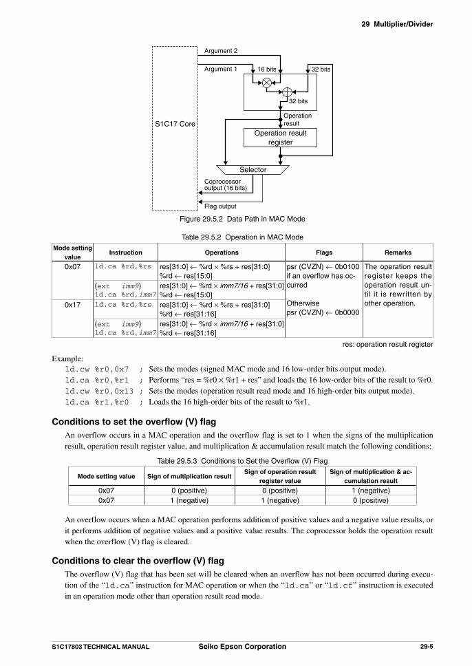
29 Multiplier/Divider
S1C17803 TECHNICAL MANUAL Seiko Epson Corporation 29-5
S1C17 CoreOperation result
register
Selector
Argument 2
Argument 1 16 bits 32 bits
32 bits
Coprocessoroutput (16 bits)
Flag output
Operationresult
Figure 29.5.2 Data Path in MAC Mode
Table 29.5.2 Operation in MAC ModeMode setting
valueInstruction Operations Flags Remarks
0x07 ld.ca %rd,%rs res[31:0] ← %rd × %rs + res[31:0]%rd ← res[15:0]
psr (CVZN) ← 0b0100 if an overflow has oc-curred
Otherwise psr (CVZN) ← 0b0000
The operation result register keeps the operation result un-til it is rewritten by other operation.
(ext imm9) ld.ca %rd,imm7
res[31:0] ← %rd × imm7/16 + res[31:0]%rd ← res[15:0]
0x17 ld.ca %rd,%rs res[31:0] ← %rd × %rs + res[31:0]%rd ← res[31:16]
(ext imm9) ld.ca %rd,imm7
res[31:0] ← %rd × imm7/16 + res[31:0]%rd ← res[31:16]
res: operation result register
Example:ld.cw %r0,0x7 ; Sets the modes (signed MAC mode and 16 low-order bits output mode).ld.ca %r0,%r1 ; Performs “res = %r0 × %r1 + res” and loads the 16 low-order bits of the result to %r0.ld.cw %r0,0x13 ; Sets the modes (operation result read mode and 16 high-order bits output mode).ld.ca %r1,%r0 ; Loads the 16 high-order bits of the result to %r1.
Conditions to set the overflow (V) flag An overflow occurs in a MAC operation and the overflow flag is set to 1 when the signs of the multiplication
result, operation result register value, and multiplication & accumulation result match the following conditions:
Table 29.5.3 Conditions to Set the Overflow (V) Flag
Mode setting value Sign of multiplication resultSign of operation result
register valueSign of multiplication & ac-
cumulation result
0x07 0 (positive) 0 (positive) 1 (negative)0x07 1 (negative) 1 (negative) 0 (positive)
An overflow occurs when a MAC operation performs addition of positive values and a negative value results, or it performs addition of negative values and a positive value results. The coprocessor holds the operation result when the overflow (V) flag is cleared.
Conditions to clear the overflow (V) flag The overflow (V) flag that has been set will be cleared when an overflow has not been occurred during execu-
tion of the “ld.ca” instruction for MAC operation or when the “ld.ca” or “ld.cf” instruction is executed in an operation mode other than operation result read mode.

29 Multiplier/Divider
29-6 Seiko Epson Corporation S1C17803 TECHNICAL MANUAL
29.6 Reading ResultsThe “ld.ca” instruction cannot load a 32-bit operation result to a CPU register, so a multiplication or MAC opera-tion returns the one-half (16 bits according to the output mode) result (A[15:0] or A[31:16]) and the flag status to the CPU registers. Another one-half should be read by setting the multiplier/divider into operation result read mode. The operation result register keeps the loaded operation result until it is rewritten by other operation.
S1C17 CoreOperation result
register
Selector
Argument 2
Argument 1
Coprocessoroutput (16 bits)
Flag output
Figure 29.6.1 Data Path in Operation Result Read Mode
Table 29.6.1 Operation in Operation Result Read ModeMode setting
valueInstruction Operations Flags Remarks
0x03 ld.ca %rd,%rs %rd ← res[15:0] psr (CVZN) ← 0b0000 This operation mode does not affect the operation result reg-ister.
ld.ca %rd,imm7 %rd ← res[15:0]0x13 ld.ca %rd,%rs %rd ← res[31:16]
ld.ca %rd,imm7 %rd ← res[31:16]
res: operation result register

30 Electrical Characteristics
S1C17803 TECHNICAL MANUAL Seiko Epson Corporation 30-1
30 Electrical Characteristics
30.1 Absolute Maximum Rating (VSS = 0V)
Item Symbol Condition Rated value Unit
Core power supply voltage LVDD -0.3 to 4.0 VRTC power supply voltage RTCVDD -0.3 to 4.0 VI/O power supply voltage HVDD HVDD = BUSIO_VDD, IO1_VDD, IO2_VDD -0.3 to 7.0 VAnalog power supply voltage AVDD -0.3 to 7.0 VRegulator power supply voltage REGU_VDD REGU_VSS = 0V -0.3 to 7.0 VInput voltage VI -0.3 to HVDD + 0.3 VOutput voltage VO -0.3 to HVDD + 0.3 VAnalog input voltage AVIN -0.3 to AVDD + 0.3 VHigh level output current IOH 1 pin -10 mA
Total of all pins -40 mALow level output current IOL 1 pin 10 mA
Total of all pins 40 mAOperating temperature Topr During Flash reading, LVDD = 2.7 to 3.6V,
FLS_WAIT[2:0] = 0x0 (0 wait)-40 to 70 °C
During Flash reading, LVDD = 3.0 to 3.6VFLS_WAIT[2:0] = 0x0 (0 wait)
-40 to 85 °C
During Flash reading, LVDD = 2.7 to 3.6VFLS_WAIT[2:0] ≥ 0x1 (1 wait or more)
-40 to 85 °C
During Flash erasing/programming -40 to 70 °CStorage temperature Tstg -65 to 150 °CSoldering temperature/time Tsol 260°C, 10 seconds
(lead section)–
30.2 Recommended Operating Conditions (Ta = -40 to 85°C)
Item Symbol Condition Min. Typ. Max. Unit
Core power supply voltage LVDD 2.7 3.0/3.3 3.6 VI/O power supply voltage HVDD HVDD = BUSIO_VDD, IO1_VDD,
IO2_VDD
2.7 – 5.5 V
Analog power supply voltage AVDD 2.7 – 5.5 VRTC power supply voltage RTCVDD 2.7 3.3 3.6 VRegulator power supply voltage REGU_VDD REGU_CE = H, REGU_VSS = 0V 4.5 5.0 5.5 VOperating frequency fOSC3 Crystal/ceramic oscillation 1 – 33 MHz
External clock input – – 33 MHzfOSC1 Crystal oscillation – 32.768 – kHz
External clock input – 32.768 – kHzInput voltage VI VSS – HVDD VInput rise time (normal input) tri – – 50 nsInput fall time (normal input) tfi – – 50 nsInput rise time (Schmitt input) tri – – 5 msInput fall time (Schmitt input) tfi – – 5 ms

30 Electrical Characteristics
30-2 Seiko Epson Corporation S1C17803 TECHNICAL MANUAL
30.3 DC CharacteristicsUnless otherwise specified: LVDD = RTCVDD = 3.0 to 3.6V, HVDD (BUSIO_VDD, IO1_VDD, IO2_VDD) = AVDD = 4.5 to 5.5V, VSS = 0V, Ta = -40 to 85°C
Item Symbol Condition Min. Typ. Max. Unit
Input leakage current ILI -1 – 1 µAOff-state leakage current IOZ -1 – 1 µAHigh level output voltage VOH IOH = -1mA (Type M),
IOH = -3mA (Type 1), HVDD = Min. HVDD
- 0.4– – V
Low level output voltage VOL IOL = 1mA (Type M), IOL = 3mA (Type 1), HVDD = Min.
– – 0.4 V
High level output voltage LVOH IOH = -2mA (Type 1), RTCVDD = Min. RTCVDD
- 0.4– – V
Low level output voltage LVOL IOL = 2mA (Type 1), RTCVDD = Min. – – 0.4 VHigh level input voltage VIH LVTTL level, HVDD = AVDD = Max. 3.5 – – VLow level input voltage VIL LVTTL level, HVDD = AVDD = Min. – – 1.0 VPositive trigger input voltage VT1+ LVTTL Schmitt 2.0 – 4.0 VNegative trigger input voltage VT1- LVTTL Schmitt 0.8 – 3.1 VHysteresis voltage VH1 LVTTL Schmitt 0.3 – – VPositive trigger input voltage VT2+ LVTTL Schmitt L 1.1 – 2.4 VNegative trigger input voltage VT2- LVTTL Schmitt L 0.6 – 1.8 VHysteresis voltage VH2 LVTTL Schmitt L 0.1 – – VPull-up resistor RPU Type 2, VI = 0V 60 120 288 kWPull-down resistor RPD Type 1, VI = 0V 30 60 144 kWInput pin capacitance CI f = 1MHz, HVDD = 0V – – 10 pFOutput pin capacitance CO f = 1MHz, HVDD = 0V – – 10 pFI/O pin capacitance CIO f = 1MHz, HVDD = 0V – – 10 pF
Unless otherwise specified: LVDD = RTCVDD = 2.7 to 3.3V, HVDD (BUSIO_VDD, IO1_VDD, IO2_VDD) = AVDD = 4.5 to 5.5V, VSS = 0V, Ta = -40 to 85°C
Item Symbol Condition Min. Typ. Max. Unit
Input leakage current ILI -1 – 1 µAOff-state leakage current IOZ -1 – 1 µAHigh level output voltage VOH IOH = -1mA (Type M),
IOH = -3mA (Type 1), HVDD = Min. HVDD
- 0.4– – V
Low level output voltage VOL IOL = 1mA (Type M), IOL = 3mA (Type 1), HVDD = Min.
– – 0.4 V
High level output voltage LVOH IOH = -1.8mA (Type 1), RTCVDD = Min.
RTCVDD
- 0.4– – V
Low level output voltage LVOL IOL = 1.8mA (Type 1), RTCVDD = Min.
– – 0.4 V
High level input voltage VIH CMOS level, HVDD = AVDD = Max. 3.5 – – VLow level input voltage VIL CMOS level, HVDD = AVDD = Min. – – 1.0 VPositive trigger input voltage VT1+ CMOS Schmitt 2.0 – 4.0 VNegative trigger input voltage VT1- CMOS Schmitt 0.8 – 3.1 VHysteresis voltage VH1 CMOS Schmitt 0.3 – – VPositive trigger input voltage VT2+ CMOS Schmitt L 1.0 – 2.3 VNegative trigger input voltage VT2- CMOS Schmitt L 0.5 – 1.7 VHysteresis voltage VH2 CMOS Schmitt L 0.1 – – VPull-up resistor RPU Type 2, VI = 0V 60 120 288 kWPull-down resistor RPD Type 1, VI = 0V 30 60 144 kWInput pin capacitance CI f = 1MHz, HVDD = 0V – – 10 pFOutput pin capacitance CO f = 1MHz, HVDD = 0V – – 10 pFI/O pin capacitance CIO f = 1MHz, HVDD = 0V – – 10 pF

30 Electrical Characteristics
S1C17803 TECHNICAL MANUAL Seiko Epson Corporation 30-3
Unless otherwise specified: LVDD = RTCVDD = 3.0 to 3.6V, HVDD (BUSIO_VDD, IO1_VDD, IO2_VDD) = AVDD = 3.0 to 3.6V, VSS = 0V, Ta = -40 to 85°C
Item Symbol Condition Min. Typ. Max. Unit
Input leakage current ILI -1 – 1 µAOff-state leakage current IOZ -1 – 1 µAHigh level output voltage VOH IOH = -1mA (Type M),
IOH = -2mA (Type 1), HVDD = Min. HVDD
- 0.4– – V
Low level output voltage VOL IOL = 1mA (Type M), IOL = 2mA (Type 1), HVDD = Min.
– – 0.4 V
High level output voltage LVOH IOH = -2mA (Type 1), RTCVDD = Min. RTCVDD
- 0.4– – V
Low level output voltage LVOL IOL = 2mA (Type 1), RTCVDD = Min. – – 0.4 VHigh level input voltage VIH LVTTL level, HVDD = AVDD = Max. 2.0 – – VLow level input voltage VIL LVTTL level, HVDD = AVDD = Min. – – 0.8 VPositive trigger input voltage VT1+ LVTTL Schmitt 1.1 – 2.4 VNegative trigger input voltage VT1- LVTTL Schmitt 0.6 – 1.8 VHysteresis voltage VH1 LVTTL Schmitt 0.1 – – VPositive trigger input voltage VT2+ LVTTL Schmitt L 1.1 – 2.4 VNegative trigger input voltage VT2- LVTTL Schmitt L 0.6 – 1.8 VHysteresis voltage VH2 LVTTL Schmitt L 0.1 – – VPull-up resistor RPU Type 2, VI = 0V 40 100 240 kWPull-down resistor RPD Type 1, VI = 0V 20 50 120 kWInput pin capacitance CI f = 1MHz, HVDD = 0V – – 10 pFOutput pin capacitance CO f = 1MHz, HVDD = 0V – – 10 pFI/O pin capacitance CIO f = 1MHz, HVDD = 0V – – 10 pF
Unless otherwise specified: LVDD = RTCVDD = 2.7 to 3.3V, HVDD (BUSIO_VDD, IO1_VDD, IO2_VDD) = AVDD = 2.7 to 3.3V, VSS = 0V, Ta = -40 to 85°C
Item Symbol Condition Min. Typ. Max. Unit
Input leakage current ILI -1 – 1 µAOff-state leakage current IOZ -1 – 1 µAHigh level output voltage VOH IOH = -1mA (Type M),
IOH = -1.8mA (Type 1), HVDD = Min. HVDD
- 0.4– – V
Low level output voltage VOL IOL = 1mA (Type M), IOL = 1.8mA (Type 1), HVDD = Min.
– – 0.4 V
High level output voltage LVOH IOH = -1.8mA (Type 1), RTCVDD = Min.
RTCVDD
- 0.4– – V
Low level output voltage LVOL IOL = 1.8mA (Type 1), RTCVDD = Min.
– – 0.4 V
High level input voltage VIH CMOS level, HVDD = AVDD = Max. 1.9 – – VLow level input voltage VIL CMOS level, HVDD = AVDD = Min. – – 0.8 VPositive trigger input voltage VT1+ CMOS Schmitt 1.0 – 2.3 VNegative trigger input voltage VT1- CMOS Schmitt 0.5 – 1.7 VHysteresis voltage VH1 CMOS Schmitt 0.1 – – VPositive trigger input voltage VT2+ CMOS Schmitt L 1.0 – 2.3 VNegative trigger input voltage VT2- CMOS Schmitt L 0.5 – 1.7 VHysteresis voltage VH2 CMOS Schmitt L 0.1 – – VPull-up resistor RPU Type 2, VI = 0V 48 120 288 kWPull-down resistor RPD Type 1, VI = 0V 24 60 144 kWInput pin capacitance CI f = 1MHz, HVDD = 0V – – 10 pFOutput pin capacitance CO f = 1MHz, HVDD = 0V – – 10 pFI/O pin capacitance CIO f = 1MHz, HVDD = 0V – – 10 pF
Note: See “Input/Output Cells and Input/Output Characteristics” in the “Pin Descriptions” section for pin characteristics.

30 Electrical Characteristics
30-4 Seiko Epson Corporation S1C17803 TECHNICAL MANUAL
Schmitt input voltageHVDD
0VT+VT-0
VIN (V)V
OU
T (
V)
HVDD
30.4 Current ConsumptionUnless otherwise specified: LVDD = RTCVDD = 3.3V, HVDD (BUSIO_VDD, IO1_VDD, IO2_VDD) = AVDD = 5.0V, VSS = 0V, Ta = -40 to 85°C, Peripheral modules: stopped
Item Symbol Condition Min. Typ. Max. Unit Powersource
Battery backup current
IBB1 OSC1: Off *4, RTC: Stop, LVDD/HVDD/AVDD: Off,STBY=Low – 0.021 – µA RTCVDDIBB2 OSC1: 32kHz, RTC: Run, LVDD/HVDD/AVDD: Off,STBY=Low – 4.9 – µA
Current consumption in SLEEP mode
ISLP1 OSC1: Off *4, OSC3: Off, RTC: Stop – 1.3 – µA LVDDISLP2 OSC1: 32kHz, OSC3: Off, RTC: Run – 5 – µA
Current consumption in HALT mode(IRAM operation) *1
IHALT11 OSC1: 32kHz, OSC3: Off, RTC: Run – 7 – µAIHALT12 OSC1: 32kHz, OSC3: 16MHz, RTC: Run – 7 – mAIHALT13 OSC1: 32kHz, OSC3: 24MHz, RTC: Run – 11 – mAIHALT14 OSC1: 32kHz, OSC3: 33MHz, RTC: Run – 15 – mA
Current consumption during execution(IRAM operation) *2
IEXE11 OSC1: 32kHz, OSC3: Off, RTC: Run – 28 – µAIEXE12 OSC1: 32kHz, OSC3: 16MHz, RTC: Run – 8 – mAIEXE13 OSC1: 32kHz, OSC3: 24MHz, RTC: Run – 12 – mAIEXE14 OSC1: 32kHz, OSC3: 33MHz, RTC: Run – 16 – mA
Current consumption during execution(Flash operation) *3
IEXE21 OSC1: 32kHz, OSC3: Off, RTC: Run – 5.9 – mAIEXE22 OSC1: 32kHz, OSC3: 16MHz, RTC: Run – 14 – mAIEXE23 OSC1: 32kHz, OSC3: 24MHz, RTC: Run – 16 – mAIEXE24 OSC1: 32kHz, OSC3: 33MHz, RTC: Run – 19 – mA
Current consumption including LCDC operating current
ILCDC1 OSC3: 33MHz, LCLK: 33MHz/6, Frame rate: 63.37Hz, 320×240-pixel 1bpp STN mono LCD panel, IVRAM is used
– 17 – mA
ILCDC2 OSC3: 33MHz, LCLK: 33MHz/6, Frame rate: 63.37Hz, 320×240-pixel 4bpp STN mono LCD panel, EVRAM is used
– 18 – mA
Current consumption includ-ing ADC10 operating current
IADC1 When ADC10 is enabled and standby, System clock: OSC1, OSC1: 32kHz, OSC3: 33MHz, RTC: Stop, Other peripheral circuits: Stop, Only ADC10 operated, Conversion clock frequency: 2MHz
– 18 – mA LVDD+
AVDD
IADC2 When ADC10 is converting,System clock: OSC1, OSC1: 32kHz, OSC3: 33MHz, RTC: Stop, Other peripheral circuits: Stop, Only ADC10 operated, Conversion clock frequency: 2MHz
– 19 – mA
RTC Current consumption
IRTC1 OSC1: 32kHz,OSC3: 33MHz, RTC: Run ,STBY=Low – 4.9 – µA RTCVDDIRTC2 OSC1: 32kHz,OSC3: 16MHz, RTC: Run ,STBY=Hi – 240 – µAIRTC3 OSC1: 32kHz,OSC3: 24MHz, RTC: Run ,STBY=Hi – 360 – µAIRTC4 OSC1: 32kHz,OSC3: 33MHz, RTC: Run ,STBY=Hi – 500 – µA

30 Electrical Characteristics
S1C17803 TECHNICAL MANUAL Seiko Epson Corporation 30-5
Item Symbol Condition Min. Typ. Max. Unit Powersource
Current consumption including Flash chip erase current
IFCERS – 43 – mA LVDD
Current consumption including Flash sector erase current
IFSERS – 44 – mA
Current consump-tion including Flash programming cur-rent
IFPRG – 37 – mA
*1) When the halt instruction is executed on the IRAM*2) When the program is executed on the IRAM*3) When the program is executed on the Flash*4) When no resonator is connected (The OSC1 oscillator circuit cannot be turned off.)
Notes: • When the halt instruction located in the Flash memory is executed, the S1C17803 enters HALT mode with the Flash area chip select signal asserted. This increases current consump-tion, as the Flash memory stays active during HALT status. Therefore, when setting the S1C17803 into HALT mode, the halt instruction should be executed in IRAM.
• The current consumption during program execution in IRAM with a high-speed clock is larger than that of the Flash. This is because the program execution speed in IRAM is higher than that in the Flash.
• The current consumption during execution in the above table indicates the value when a test program that consists of 51% load instructions, 21% arithmetic operation instructions, 10% branch instructions and 18% ext instructions is being executed in the built-in memory (IRAM or Flash).
Current consumption - frequency characteristic during execution (Flash operation) LVDD = 3.3V, Ta = 25°C, Typ. value
0 10 20 30 40
20
18
16
14
12
10
8
6
4
2
0
OSC3 frequency [MHz]
IEX
E2
[mA
]
(1) FLS_WAIT[2:0] = 0 (0 wait cycles)(2) FLS_WAIT[2:0] = 1 (1 wait cycle)
(1)
(2)

30 Electrical Characteristics
30-6 Seiko Epson Corporation S1C17803 TECHNICAL MANUAL
Current consumption - frequency characteristic during execution (IRAM operation) LVDD = 3.3V, Ta = 25°C, Typ. value
0 5 10 15 20 25 30 35
18
16
14
12
10
8
6
4
2
0
OSC3 frequency [MHz]
IEX
E1
[mA
]
Current consumption - frequency characteristic in HALT mode
(when the halt instruction is executed in IRAM) LVDD = 3.3V, Ta = 25°C, Typ. value
IHA
LT1
[mA
]
0 5 10 15 20 25 30 35
16
14
12
10
8
6
4
2
0
OSC3 frequency [MHz]
30.5 A/D Converter CharacteristicsUnless otherwise specified: LVDD = 2.7 to 3.6V, HVDD (BUSIO_VDD, IO1_VDD, IO2_VDD) = AVDD = 2.7 to 5.5V, VSS = 0V, Ta = -20 to 70°C, ADST[2:0] = 0x7
Item Symbol Condition Min. Typ. Max. Unit
Resolution – – 10 – bitsA/D conversion clock fADCLK 16 – 2000 kHzSampling rate *1 – 0.8 – 100 kspsZero-scale error EZS – – ±3 LSBFull-scale error EFS – – ±3 LSBIntegral linearity error *2 EINL – – ±1.5 LSBDifferential linearity error EDNL – – ±1.0 LSBAnalog input resistance RAIN – – 11 kWAnalog input capacitance CAIN – – 20 pF
*1 Condition for Max. value: A/D converter clock input = 2MHz. Condition for Min. value: A/D converter clock input = 16kHz.
*2 Integral linearity error is measured at the end point line.

30 Electrical Characteristics
S1C17803 TECHNICAL MANUAL Seiko Epson Corporation 30-7
30.6 Oscillation CharacteristicsOscillation characteristics vary depending on conditions such as components used (resonator, Rf, Rd, CG, CD) and board pattern. Use the following characteristics as reference values. In particular, when a ceramic or crystal resona-tor is used, evaluate the components adequately under real operating conditions by mounting them on the board before the external register (Rf, Rd) and capacitor (CG, CD) values are finally decided.
OSC1 crystal oscillationUnless otherwise specified: LVDD = RTCVDD = 3.3V, VSS = 0V, Ta = 25°C
Item Symbol Condition Min. Typ. Max. Unit
Oscillation start time tSTA1 *1 – – 3 s
OSC3 crystal oscillationNote: A “crystal resonator that uses a fundamental” should be used for the OSC3 crystal oscillation cir-
cuit.
Unless otherwise specified: LVDD = 3.3V, VSS = 0V, Ta = 25°CItem Symbol Condition Min. Typ. Max. Unit
Oscillation start time tSTA3 *1 – – 10 ms
OSC3 ceramic oscillationUnless otherwise specified: LVDD = 3.3V, VSS = 0V, Ta = 25°C
Item Symbol Condition Min. Typ. Max. Unit
Oscillation start time tSTA3 *1 – – 5 ms
*1) When the recommended parts shown in the “Basic External Wiring Diagram” chapter are used
30.7 AC Characteristics
30.7.1 External Clock Input Characteristics
OSC1/OSC3
tC1/tC3
tC1H/tC3H tC1ED = tC1H/tC1
tC3ED = tC3H/tC3
tIF tIR
OSC1 external clockUnless otherwise specified: LVDD = RTCVDD = 2.7 to 3.6V, VSS = 0V, Ta = 0 to 70°C
Item Symbol Min. Typ. Max. Unit
OSC1 external clock cycle time tC1 – 30.51 – µsOSC1 external clock input duty tC1ED 45 – 55 %OSC1 external clock input rise time tIF – – 5 nsOSC1 external clock input fall time tIR – – 5 ns
OSC3 external clockUnless otherwise specified: IO1_VDD = 2.7 to 5.5V, VSS = 0V, Ta = 0 to 70°C
Item Symbol Min. Typ. Max. Unit
OSC3 external clock cycle time tC3 30.30 – 1000 nsOSC3 external clock input duty tC3ED 45 – 55 %OSC3 external clock input rise time tIF – – 5 nsOSC3 external clock input fall time tIR – – 5 ns

30 Electrical Characteristics
30-8 Seiko Epson Corporation S1C17803 TECHNICAL MANUAL
30.7.2 SRAMC AC Characteristics
SRAM read cycle
OSC3
CMU_CLK
#CEx
A[22:0]
#RD
D[15:0]
#WAIT
tCD tCYC
tRDD tRDC
tWTS tWTH
tRDS
tRRT
tRDH
tCED
tAD
SRAM write cycle
OSC3
CMU_CLK
#CEx
A[22:0]
#WR
D[15:0]
#WAIT
tCD tCYC
tWRD tWRC
tWTS tWTH
tWRT
tWRDH
tCED
tAD
tWRDD
Unless otherwise specified: LVDD = 2.7 to 3.6V, BUSIO_VDD = 4.5 to 5.5V, VSS = 0VItem Symbol Min. Typ. Max. Unit
CMU_CLK output delay time tCD – – 60 ns#CEx delay time from CMU_CLK rise tCED – – 17 nsAddress delay time tAD – – 5 nsWrite delay time tWRD – – tCYC nsWrite pulse width tWRC – – tW + tCYC nsWrite rise to #CEx rise time tWRT – – tCYC nsWrite data delay time tWRDD – – 0 nsWrite data hold time tWRDH 5 – – nsRead delay time tRDD – – tCYC nsRead pulse width tRDC – – tW + tCYC nsRead rise to #CEx rise time tRRT – – tCYC nsRead data setup time tRDS 45 – – nsRead data hold time tRDH 0 – – ns#WAIT setup time tWTS 90 – – ns#WAIT hold time tWTH 0 – – ns

30 Electrical Characteristics
S1C17803 TECHNICAL MANUAL Seiko Epson Corporation 30-9
Unless otherwise specified: LVDD = 2.7 to 3.6V, BUSIO_VDD = 2.7 to 3.6V, VSS = 0VItem Symbol Min. Typ. Max. Unit
CMU_CLK output delay time tCD – – 65 ns#CEx delay time from CMU_CLK rise tCED – – 20 nsAddress delay time tAD – – 7 nsWrite delay time tWRD – – tCYC nsWrite pulse width tWRC – – tW + tCYC nsWrite rise to #CEx rise time tWRT – – tCYC nsWrite data delay time tWRDD – – 0 nsWrite data hold time tWRDH 5 – – nsRead delay time tRDD – – tCYC nsRead pulse width tRDC – – tW + tCYC nsRead rise to #CEx rise time tRRT – – tCYC nsRead data setup time tRDS 55 – – nsRead data hold time tRDH 0 – – ns#WAIT setup time tWTS 95 – – ns#WAIT hold time tWTH 0 – – ns
tW: wait cycle timetCYC: System clock cycle time

30 Electrical Characteristics
30-10 Seiko Epson Corporation S1C17803 TECHNICAL MANUAL
30.7.3 USI AC Characteristics
SPI master/slave mode
spi_sck (US_SCKx)(falling edge sampling)
spi_sck (US_SCKx)(rising edge sampling)
spi_sdi (US_SDIx)
spi_sdo (US_SDOx)
tSPCK
tSDO tSDH
tSDS
SPI master mode (8 or 9 bits, normal mode)Unless otherwise specified: LVDD = 2.7 to 3.6V, IO1_VDD/IO2_VDD= 4.5 to 5.5V, VSS = 0V
Item Symbol Min. Typ. Max. Unit
spi_sck cycle time tSPCK 85 + tPCLK – – nsspi_sdi setup time tSDS 85 + tPCLK – – nsspi_sdi hold time tSDH 0 – – nsspi_sdo output delay time tSDO – – 20 ns
Unless otherwise specified: LVDD = 2.7 to 3.6V, IO1_VDD/IO2_VDD= 2.7 to 3.6V, VSS = 0VItem Symbol Min. Typ. Max. Unit
spi_sck cycle time tSPCK 85 + tPCLK – – nsspi_sdi setup time tSDS 85 + tPCLK – – nsspi_sdi hold time tSDH 0 – – nsspi_sdo output delay time tSDO – – 15 ns
SPI master mode (8 or 9 bits, fast mode)Unless otherwise specified: LVDD = 2.7 to 3.6V, IO1_VDD/IO2_VDD= 4.5 to 5.5V, VSS = 0V
Item Symbol Min. Typ. Max. Unit
spi_sck cycle time tSPCK 85 – – nsspi_sdi setup time tSDS 85 – – nsspi_sdi hold time tSDH 0 – – nsspi_sdo output delay time tSDO – – 10 ns
Unless otherwise specified: LVDD = 2.7 to 3.6V, IO1_VDD/IO2_VDD= 2.7 to 3.6V, VSS = 0VItem Symbol Min. Typ. Max. Unit
spi_sck cycle time tSPCK 85 – – nsspi_sdi setup time tSDS 85 – – nsspi_sdi hold time tSDH 0 – – nsspi_sdo output delay time tSDO – – 10 ns
SPI slave modeUnless otherwise specified: LVDD = 2.7 to 3.6V, IO1_VDD/IO2_VDD= 4.5 to 5.5V, VSS = 0V
Item Symbol Min. Typ. Max. Unit
spi_sck cycle time tSPCK *2 – – nsspi_sdi setup time tSDS 10 + tPCLK – – nsspi_sdi hold time tSDH 10 – – nsspi_sdo output delay time tSDO – – 80 ns
Unless otherwise specified: LVDD = 2.7 to 3.6V, IO1_VDD/IO2_VDD= 2.7 to 3.6V, VSS = 0VItem Symbol Min. Typ. Max. Unit
spi_sck cycle time tSPCK *2 – – nsspi_sdi setup time tSDS 10 + tPCLK – – nsspi_sdi hold time tSDH 10 – – nsspi_sdo output delay time tSDO – – 80 ns
*1) tPCLK: PCLK1 or PCLK2 (peripheral module clock supplied from the CMU) clock cycle time*2) tSPCK(min.) = 80ns if tPCLK ≤ 60ns or tSPCK(min.) = “20 + tPCLK” ns if tPCLK > 60ns

30 Electrical Characteristics
S1C17803 TECHNICAL MANUAL Seiko Epson Corporation 30-11
I2C master/slave mode
tREP
tSDO tSPHtSTH
T8F output clock
i2c_scl (US_SCKx) (master)
i2c_scl (US_SCKx) (slave)
i2c_sda (US_SDIx/#US_SSIx) input
i2c_sda (US_SDIx/#US_SSIx) output
Input data sampling pointfor master and slave
I2C master modeUnless otherwise specified: LVDD = 2.7 to 3.6V, IO1_VDD/IO2_VDD= 4.5 to 5.5V, VSS = 0V
Item Symbol Min. Typ. Max. Unit
i2c_scl cycle time tSCL 2500 – – nsi2c_sda output delay time tSDO – – 2*tT8 nsStart condition hold time tSTH 4*tT8 – – nsStop condition hold time tSPH 3*tT8 – – ns
Unless otherwise specified: LVDD = 2.7 to 3.6V, IO1_VDD/IO2_VDD= 2.7 to 3.6V, VSS = 0VItem Symbol Min. Typ. Max. Unit
i2c_scl cycle time tSCL 2500 – – nsi2c_sda output delay time tSDO – – 2*tT8 nsStart condition hold time tSTH 4*tT8 – – nsStop condition hold time tSPH 3*tT8 – – ns
I2C slave modeUnless otherwise specified: LVDD = 2.7 to 3.6V, IO1_VDD/IO2_VDD= 4.5 to 5.5V, VSS = 0V
Item Symbol Min. Typ. Max. Unit
i2c_scl cycle time tSCL 2500 – – nsi2c_scl input clock response delay time tREP – – 4*tT8 nsi2c_sda output delay time tSDO – – 2*tT8 nsStart condition hold time tSTH 7*tPCLK – – nsStop condition hold time tSPH 7*tPCLK – – ns
Unless otherwise specified: LVDD = 2.7 to 3.6V, IO1_VDD/IO2_VDD= 2.7 to 3.6V, VSS = 0VItem Symbol Min. Typ. Max. Unit
i2c_scl cycle time tSCL 2500 – – nsi2c_scl input clock response delay time tREP – – 4*tT8 nsi2c_sda output delay time tSDO – – 2*tT8 nsStart condition hold time tSTH 7*tPCLK – – nsStop condition hold time tSPH 7*tPCLK – – ns
tPCLK: PCLK1 or PCLK2 (peripheral module clock supplied from the CMU) clock cycle timetT8 = T8F output clock cycle time
30.7.4 I2CM/I2CS AC Characteristics
T8F output clock
SCL (I2CM_SCL) (master)
SCL (I2CS_SCL) (slave)
SDA (I2CM_SDA/I2CS_SDA) input
SDA (I2CM_SDA/I2CS_SDA) output
tREP
tSDS tSDH
tSDO tSPHtSTH
I2CSinput data sampling point
I2CMinput data sampling point

30 Electrical Characteristics
30-12 Seiko Epson Corporation S1C17803 TECHNICAL MANUAL
I2CM (noise filter on)Unless otherwise specified: LVDD = 2.7 to 3.6V, IO1_VDD/IO2_VDD= 4.5 to 5.5V, VSS = 0V
Item Symbol Min. Typ. Max. Unit
SCL clock cycle time tSCL 2500 – – nsSDA input hold time tSDH 10 – – nsSDA output delay time tSDO – – tT8 nsStart condition hold time tSTH tT8 – – nsStop condition hold time tSPH tT8 – – ns
Unless otherwise specified: LVDD = 2.7 to 3.6V, IO1_VDD/IO2_VDD= 2.7 to 3.6V, VSS = 0VItem Symbol Min. Typ. Max. Unit
SCL clock cycle time tSCL 2500 – – nsSDA input hold time tSDH 10 – – nsSDA output delay time tSDO – – tT8 nsStart condition hold time tSTH tT8 – – nsStop condition hold time tSPH tT8 – – ns
I2CM (noise filter off)Unless otherwise specified: LVDD = 2.7 to 3.6V, IO1_VDD/IO2_VDD= 4.5 to 5.5V, VSS = 0V
Item Symbol Min. Typ. Max. Unit
SCL clock cycle time tSCL 2500 – – nsSDA input hold time tSDH 10 – – nsSDA output delay time tSDO – – tT8 nsStart condition hold time tSTH tT8 – – nsStop condition hold time tSPH tT8 – – ns
Unless otherwise specified: LVDD = 2.7 to 3.6V, IO1_VDD/IO2_VDD= 2.7 to 3.6V, VSS = 0VItem Symbol Min. Typ. Max. Unit
SCL clock cycle time tSCL 2500 – – nsSDA input hold time tSDH 10 – – nsSDA output delay time tSDO – – tT8 nsStart condition hold time tSTH tT8 – – nsStop condition hold time tSPH tT8 – – ns
I2CSUnless otherwise specified: LVDD = 2.7 to 3.6V, IO1_VDD/IO2_VDD= 4.5 to 5.5V, VSS = 0V
Item Symbol Min. Typ. Max. Unit
SCL clock cycle time tSCL 2500 – – nsSCL input clock response delay time tREP 80 + tPCLK – – nsSDA input setup time tSDS 30 – – nsSDA output delay time tSDO – – 80 nsStart condition hold time tSTH tPCLK – – nsStop condition hold time tSPH tPCLK – – ns
Unless otherwise specified: LVDD = 2.7 to 3.6V, IO1_VDD/IO2_VDD= 2.7 to 3.6V, VSS = 0VItem Symbol Min. Typ. Max. Unit
SCL clock cycle time tSCL 2500 – – nsSCL input clock response delay time tREP 80 + tPCLK – – nsSDA input setup time tSDS 30 – – nsSDA output delay time tSDO – – 80 nsStart condition hold time tSTH tPCLK – – nsStop condition hold time tSPH tPCLK – – ns
tPCLK: PCLK_SOC (peripheral module clock supplied from the CMU) clock cycle timetT8 = T8F output clock cycle time

30 Electrical Characteristics
S1C17803 TECHNICAL MANUAL Seiko Epson Corporation 30-13
30.7.5 LCDC AC Characteristics
4-bit single monochrome panel timing
FPFRAME
FPLINE
FPDRDY (MOD)
FPDAT[7:4]
VDP VNDP
FPLINE
FPDRDY (MOD)
FPSHIFT
FPDAT7
FPDAT6
FPDAT5
FPDAT4
Line 1
1-1 1-5 1-317
1-2 1-6 1-318
1-3 1-7 1-319
1-4 1-8 1-320
Line 2 Line 3 Line 1 Line 2Line 4 Line 239 Line 240
HDP HNDP
* Diagram drawn with 2 FPLINE vertical blank period Example timing for a 320 × 240 panel For this timing diagram FPSMASK is set to 1
HDP (Horizontal Display Period) = (HSIZE[6:0] + 1) × 8 (Ts)HNDP (Horizontal Non-Display Period) = (HNDP[4:0] + 4) × 8 (Ts)VDP (Vertical Display Period) = VSIZE[9:0] + 1 (lines)VNDP (Vertical Non-Display Period) = VNDP[5:0] (lines)
Frame Pulse
Line Pulse
FPDRDY (MOD)
Sync Timing
21
t2t1
t5
t6 t8 t9t7 t14 t11 t10
t12 t13
t4 t3
Line Pulse
Shift Pulse
FPDAT[7:4]
Data Timing

30 Electrical Characteristics
30-14 Seiko Epson Corporation S1C17803 TECHNICAL MANUAL
Symbol Parameter Min. Typ. Max. Unit
t1 Frame Pulse setup to Line Pulse falling edge note 2 (note 1)t2 Frame Pulse hold from Line Pulse falling edge 9 Tst3 Line Pulse period note 3t4 Line Pulse width 9 Tst5 MOD delay from Line Pulse rising edge 1 Tst6 Shift Pulse falling edge to Line Pulse rising edge note 4t7 Shift Pulse falling edge to Line Pulse falling edge note 5t8 Line Pulse falling edge to Shift Pulse falling edge t14 + 2 Tst9 Shift Pulse period 4 Tst10 Shift Pulse width low 2 Tst11 Shift Pulse width high 2 Tst12 FPDAT[7:4] setup to Shift Pulse falling edge 2 Tst13 FPDAT[7:4] hold from Shift Pulse falling edge 2 Tst14 Line Pulse falling edge to Shift Pulse rising edge 23 Ts
note) 1. Ts = pixel clock period 2. t1min = t3min - 9 (Ts) 3. t3min = HDP + HNDP (Ts) 4. t6min = HNDP + 2 (Ts) 5. t7min = HNDP + 11 (Ts)
8-bit single monochrome panel timing
FPFRAME
FPLINE
FPDRDY (MOD)
FPDAT[7:0]
VDP VNDP
FPLINE
FPDRDY (MOD)
FPSHIFT
FPDAT7
FPDAT6
FPDAT5
FPDAT4
FPDAT3
FPDAT2
FPDAT1
FPDAT0
Line 1
1-1 1-9 1-313
1-2 1-10 1-314
1-3 1-11 1-315
1-4 1-12 1-316
1-5 1-13 1-317
1-6 1-14 1-318
1-7 1-15 1-319
1-8 1-16 1-320
Line 2 Line 3 Line 1 Line 2Line 4 Line 239 Line 240
HDP HNDP
* Diagram drawn with 2 FPLINE vertical blank period Example timing for a 320 × 240 panel For this timing diagram FPSMASK is set to 1
HDP (Horizontal Display Period) = (HSIZE[6:0] + 1) × 8 (Ts)HNDP (Horizontal Non-Display Period) = (HNDP[4:0] + 4) × 8 (Ts)VDP (Vertical Display Period) = VSIZE[9:0] + 1 (lines)VNDP (Vertical Non-Display Period) = VNDP[5:0] (lines)

30 Electrical Characteristics
S1C17803 TECHNICAL MANUAL Seiko Epson Corporation 30-15
Frame Pulse
Line Pulse
FPDRDY (MOD)
Sync Timing
21
t2t1
t5
t6 t8 t9t7 t14 t11 t10
t12 t13
t4 t3
Line Pulse
Shift Pulse
FPDAT[7:0]
Data Timing
Symbol Parameter Min. Typ. Max. Unit
t1 Frame Pulse setup to Line Pulse falling edge note 2 (note 1)t2 Frame Pulse hold from Line Pulse falling edge 9 Tst3 Line Pulse period note 3t4 Line Pulse width 9 Tst5 MOD delay from Line Pulse rising edge 1 Tst6 Shift Pulse falling edge to Line Pulse rising edge note 4t7 Shift Pulse falling edge to Line Pulse falling edge note 5t8 Line Pulse falling edge to Shift Pulse falling edge t14 + 4 Tst9 Shift Pulse period 8 Tst10 Shift Pulse width low 4 Tst11 Shift Pulse width high 4 Tst12 FPDAT[7:0] setup to Shift Pulse falling edge 4 Tst13 FPDAT[7:0] hold from Shift Pulse falling edge 4 Tst14 Line Pulse falling edge to Shift Pulse rising edge 23 Ts
note) 1. Ts = pixel clock period 2. t1min = t3min - 9 (Ts) 3. t3min = HDP + HNDP (Ts) 4. t6min = HNDP + 4 (Ts) 5. t7min = HNDP + 13 (Ts)

30 Electrical Characteristics
30-16 Seiko Epson Corporation S1C17803 TECHNICAL MANUAL
30.7.6 #STBY AC Characteristics
LVDD
RTCVDD
#STBY
2.7V 2.7V 2.7V
t BUPPO t BUPS t BUPH
VIHVIL
Power On
Normal operation state Backup state
Unless otherwise specified: LVDD = 2.7~ 3.6V, IO1_VDD/ IO2_VDD=4.5~ 5.5V, VSS=0VItem Symbol Min. Typ. Max. Unit Remarks
Power discontinuity time when entering backup state tBUPS 100 – – ns *1Power supply stability time when returning from backup state tBUPH 100 – – ns *2
*1) When entering backup state, set the #STBY pin to low level to meet the AC characteristics before the LVDD becomes lower than 2.7 V.
*2) When returning from backup state, set the #STBY pin to high level after the LVDD becomes more than 2.7 V.

31 Basic External Connection Diagram
S1C17803 TECHNICAL MANUAL Seiko Epson Corporation 31-1
31 Basic External Connection Diagram3 V single power supply (internal regulator is not used)
Externalbus
A[22:1], A0/#BSLD[15:0]
#RD#WRL
#WRH/#BSH#CEx
#WAIT#NMI
CMU_CLKWDT_CLK
#WDT_NMI
FPFRAMEFPLINE
FPDAT[7:0]FPSHIFTFPDRDY
SINSOUT
#SCLK
US_SDIxUS_SDOxUS_SCKx#US_SSIx
I2CM_SDAI2CM_SCL
I2CS_SDAI2CS_SCL
#I2CS_BRST
#SMRD#SMWR
I2S_SDOI2S_WS
I2S_SCKI2S_MCLK
#ADTRGAINx
EXCL0TMHTML
EXCL1ATMAATMB
REMC_INREMC_OUT
Pxx
LCD panel
Card
I2S
A/D input
16-bit PWM timer input/output
I/O
Serial I/O(UART, SPI, I2C)
Serial I/O(UART)
Remote transmitter/receiver
16-bit audio PWM timer input/output
S1C17803[The potential of the substrate
(back of the chip) is VSS.]
REGU_VDD
REGU_CE
LVDD
RTCVDD
BUSIO_VDD
IO1_VDD
IO2_VDD
AVDD
TVEP
OSC3
OSC4
OSC1
OSC2
#RESET
TEST
VSS
REGU_VSS
DSIO
DCLK
DST2
Cres
3.3 V CP+
CG2
Rf2X’tal2 orCeramic
CD2
CG1
Rf1
Rd2
Rd1
X’tal1
CD1
Leave the pins open oruse as debug pins
Pull up or useas a debug pin
10kVDD
I2C master
I2C slave

31 Basic External Connection Diagram
31-2 Seiko Epson Corporation S1C17803 TECHNICAL MANUAL
5 V and 3 V dual power supply (internal regulator is not used)
Externalbus
A[22:1], A0/#BSLD[15:0]
#RD#WRL
#WRH/#BSH#CEx
#WAIT#NMI
CMU_CLKWDT_CLK
#WDT_NMI
FPFRAMEFPLINE
FPDAT[7:0]FPSHIFTFPDRDY
SINSOUT
#SCLK
US_SDIxUS_SDOxUS_SCKx#US_SSIx
I2CM_SDAI2CM_SCL
I2CS_SDAI2CS_SCL
#I2CS_BRST
#SMRD#SMWR
I2S_SDOI2S_WS
I2S_SCKI2S_MCLK
#ADTRGAINx
EXCL0TMHTML
EXCL1ATMAATMB
REMC_INREMC_OUT
Pxx
LCD panel
Card
I2S
A/D input
16-bit PWM timer input/output
I/O
Serial I/O(UART, SPI, I2C)
Serial I/O(UART)
Remote transmitter/receiver
16-bit audio PWM timer input/output
S1C17803[The potential of the substrate
(back of the chip) is VSS.]
REGU_VDD
REGU_CE
LVDD
RTCVDD
BUSIO_VDD
IO1_VDD
IO2_VDD
AVDD
TVEP
OSC3
OSC4
OSC1
OSC2
#RESET
TEST
VSS
REGU_VSS
DSIO
DCLK
DST2
Cres
3.3 V
5.0 V
CP+
+
CG2
Rf2X’tal2 orCeramic
CD2
CG1
Rf1
Rd2
Rd1
X’tal1
CD1
Leave the pins open oruse as debug pins
Pull up or useas a debug pin
10kVDD
I2C master
I2C slave

31 Basic External Connection Diagram
S1C17803 TECHNICAL MANUAL Seiko Epson Corporation 31-3
5 V single power supply (internal regulator is used)
Externalbus
A[22:1], A0/#BSLD[15:0]
#RD#WRL
#WRH/#BSH#CEx
#WAIT#NMI
CMU_CLKWDT_CLK
#WDT_NMI
FPFRAMEFPLINE
FPDAT[7:0]FPSHIFTFPDRDY
SINSOUT
#SCLK
US_SDIxUS_SDOxUS_SCKx#US_SSIx
I2CM_SDAI2CM_SCL
I2CS_SDAI2CS_SCL
#I2CS_BRST
#SMRD#SMWR
I2S_SDOI2S_WS
I2S_SCKI2S_MCLK
#ADTRGAINx
EXCL0TMHTML
EXCL1ATMAATMB
REMC_INREMC_OUT
Pxx
LCD panel
Card
I2S
A/D input
16-bit PWM timer input/output
I/O
I2C master
Serial I/O(UART, SPI, I2C)
Serial I/O(UART)
I2C slave
Remote transmitter/receiver
16-bit audio PWM timer input/output
S1C17803[The potential of the substrate
(back of the chip) is VSS.]
BUSIO_VDD
IO1_VDD
IO2_VDD
AVDD
TVEP
REGU_CE
REGU_VDD
LVDD
RTCVDD
OSC3
OSC4
OSC1
OSC2
#RESET
TEST
VSS
REGU_VSS
DSIO
DCLK
DST2
Cres
5.0 V CP+
CREGU
CLVDD
Rf2X'tal2 orCeramic
CD2
CG1
Rf1
Rd2
Rd1
X'tal1
CD1
Leave the pins open oruse as debug pins
Pull up or useas a debug pin
10kVDD

31 Basic External Connection Diagram
31-4 Seiko Epson Corporation S1C17803 TECHNICAL MANUAL
Recommended values for external partsExternal parts for the OSC1 oscillator circuit
Symbol Resonator Recommended manufacturerFrequency
[Hz]Product number
Recommended values
Recommended operating condition
CD1
[pF]CG1
[pF]Rf1
[W]Rd1
[W]Temperature range
[°C]X'tal1 Crystal Epson Toyocom Corporation 32.768k *1 – – – – –
(Reference values) 32.768k – 10 10 10M 0 -40 to 85
*1 Please contact the recommended manufacturer.
External parts for the OSC3 oscillator circuit
Symbol Resonator Recommended manufacturerFrequency
[Hz]Product number
Recommended values *2
Recommended operating condition
CD2
[pF]CG2
[pF]Rf2
[W]Rd2
[W]Temperature range
[°C]X'tal2 Crystal Epson Toyocom Corporation 1M to 33M *1 – – – – –
(Reference values) 1M to 33M – 15 15 1M 0 -40 to 85Ceramic Ceramic Murata Manufacturing Co., Ltd. 1M CSBFB1M00J58-R1
[SMD]330 330 1M 680 -20 to 80
1M CSBLA1M00J58-B0 [leaded]
330 330 1M 680 -20 to 80
4M CSTCR4M00G55-R0 [leaded]
(39) (39) 1M 470 -20 to 80
4M CSTLS4M00G56-B0 [leaded]
(47) (47) 1M 330 -20 to 80
10M CSTCE10M0G55-R0 [SMD]
(33) (33) 1M 220 -20 to 80
10M CSTLS10M0G56-B0 [leaded]
(47) (47) 1M 220 -20 to 80
20M CSTCE20M0V53-R0 [SMD]
(15) (15) 1M 0 -20 to 80
20M CSTCG20M0V53-R0 [small SMD]
(15) (15) 1M 0 -20 to 80
*1 Please contact the recommended manufacturer.*2 The CD2 and CG2 values enclosed with ( ) are the built-in capacitances of the resonator.
OtherSymbol Name Recommended valueCP Capacitor for power supply 3.3 µFCres Capacitor for #RESET pin 0.47 µFCLVDD Capacitor for LVDD 4.7 µFCREGU Capacitor for Regulator 1.0 µF
Notes: • The values in the above table are shown only for reference and not guaranteed.
• Crystal and ceramic resonators are extremely sensitive to influence of external components and printed-circuit boards. Before using a resonator, please contact the manufacturer for fur-ther information on conditions of use.

Appendix A: List of I/O Registers
S1C17803 TECHNICAL MANUAL Seiko Epson Corporation AP-1
Appendix A: List of I/O RegistersInternal peripheral circuit area 1 (0x4000–0x43ff)
Peripheral Address Register name FunctionPrescaler Ch.0(8-bit device)
0x4020 PSC_CTL0 PSC Ch.0 Control Register Starts/stops the PSC Ch.0.
UART (with IrDA) (8-bit device)
0x4100 UART_ST UART Status Register Indicates transfer, buffer and error statuses.0x4101 UART_TXD UART Transmit Data Register Transmit data0x4102 UART_RXD UART Receive Data Register Receive data0x4103 UART_MOD UART Mode Register Sets transfer data format.0x4104 UART_CTL UART Control Register Controls data transfer.0x4105 UART_EXP UART Expansion Register Sets IrDA mode.
CLG_T16FU0(16-bit device)
0x4200 CLG_T16FU0_CLK
CLG_T16FU0 Input Clock Select Register Selects a prescaler output clock.
0x4202 CLG_T16FU0_TR
CLG_T16FU0 Reload Data Register Sets reload data.
0x4204 CLG_T16FU0_TC
CLG_T16FU0 Counter Data Register Counter data
0x4206 CLG_T16FU0_CTL
CLG_T16FU0 Control Register Sets the timer mode and starts/stops the timer.
0x4208 CLG_T16FU0_INT
CLG_T16FU0 Interrupt Control Register Controls the interrupt.
CLG_T8I(16-bit device)
0x4260 CLG_T8I_CLK
CLG_T8I Input Clock Select Register Selects a prescaler output clock.
0x4262 CLG_T8I_TR CLG_T8I Reload Data Register Sets reload data.0x4264 CLG_T8I_TC CLG_T8I Counter Data Register Counter data0x4266 CLG_T8I_CTL CLG_T8I Control Register Sets the timer mode and starts/stops the timer.0x4268 CLG_T8I_INT CLG_T8I Interrupt Control Register Controls the interrupt.
Interrupt controller(16-bit device)
0x42e6 ITC_LV0 Interrupt Level Setup Register 0 Sets the DMA and port 0 interrupt levels.0x42e8 ITC_LV1 Interrupt Level Setup Register 1 Sets the port 1/T16A and USI Ch.0 interrupt
levels.0x42ea ITC_LV2 Interrupt Level Setup Register 2 Sets the USI Ch.1 and ADC interrupt levels.0x42ec ITC_LV3 Interrupt Level Setup Register 3 Sets the T16P/I2S and LCDC interrupt levels.0x42ee ITC_LV4 Interrupt Level Setup Register 4 Sets the CLG_T16FU0 interrupt level.0x42f0 ITC_LV5 Interrupt Level Setup Register 5 Sets the CLG_T8I interrupt level.0x42f2 ITC_LV6 Interrupt Level Setup Register 6 Sets the UART interrupt level.0x42f4 ITC_LV7 Interrupt Level Setup Register 7 Sets the I2CM interrupt level.0x42f6 ITC_LV8 Interrupt Level Setup Register 8 Sets the I2CS and T8F Ch.0–2/T16A interrupt
levels.0x42f8 ITC_LV9 Interrupt Level Setup Register 9 Sets the RTC and REMC interrupt levels.
I2C master(16-bit device)
0x4340 I2CM_EN I2C Master Enable Register Enables the I2C master module.0x4342 I2CM_CTL I2C Master Control Register Controls the I2C master operation and indicates
transfer status.0x4344 I2CM_DAT I2C Master Data Register Transmit/receive data0x4346 I2CM_ICTL I2C Master Interrupt Control Register Controls the I2C master interrupt.
I2C slave(16-bit device)
0x4360 I2CS_TRNS I2C Slave Transmit Data Register I2C slave transmit data0x4362 I2CS_RECV I2C Slave Receive Data Register I2C slave receive data0x4364 I2CS_SADRS I2C Slave Address Setup Register Sets the I2C slave address.0x4366 I2CS_CTL I2C Slave Control Register Controls the I2C slave module.0x4368 I2CS_STAT I2C Slave Status Register Indicates the I2C bus status.0x436a I2CS_ASTAT I2C Slave Access Status Register Indicates the I2C slave access status.0x436c I2CS_ICTL I2C Slave Interrupt Control Register Controls the I2C slave interrupt.
Internal Peripheral Circuit Area 2 (0x5000–0x5fff)Peripheral Address Register name Function
MISC registers(8-bit device)
0x5324 MISC_PROT MISC Protect Register Enables writing to the MISC registers.0x5328 MISC_TTBRL Vector Table Address Low Register Sets vector table address.0x532a MISC_TTBRH Vector Table Address High Register0x532c MISC_PSR PSR Register Indicates the S1C17 Core PSR values.
Internal Peripheral Circuit Area 3 (0x80000–0x82fff)Peripheral Address Register name Function
Clock management unit(8-bit device)
0x80000 CMU_OSC-SRC
Clock Source Select Register Selects the system clock source.
0x80001 CMU_OS-CCTL
Oscillation Control Register Controls oscillation.
0x80002 CMU_NFEN Noise Filter Enable Register Enables noise filters.
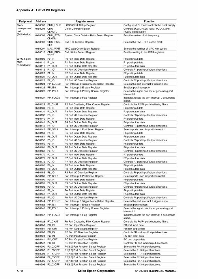
Appendix A: List of I/O Registers
AP-2 Seiko Epson Corporation S1C17803 TECHNICAL MANUAL
Peripheral Address Register name FunctionClock management unit(8-bit device)
0x80003 CMU_LCLK LCDC Clock Setup Register Configures LCLK and controls the clock supply.0x80004 CMU_
CLKCTLClock Control Register Controls BCLK, PCLK_SOC, PCLK1, and
PCLK2 clock supply.0x80005 CMU_SYS-
CLKDIVSystem Clock Division Ratio Select Register Sets the system clock frequency.
0x80006 CMU_CMU-CLK
CMU_CLK Select Register Selects the CMU_CLK output clock.
0x80007 MAC_WAIT MAC Wait Cycle Select Register Selects the number of MAC wait cycles.0x80010 CMU_PRO-
TECTCMU Write Protect Register Enables writing to the CMU registers.
GPIO & port MUX(8-bit device)
0x80100 P0_IN P0 Port Input Data Register P0 port input data0x80110 P1_IN P1 Port Input Data Register P1 port input data0x80111 P1_OUT P1 Port Output Data Register P1 port output data0x80112 P1_IO P1 Port I/O Direction Register Controls P1 port input/output directions.0x80120 P2_IN P2 Port Input Data Register P2 port input data0x80121 P2_OUT P2 Port Output Data Register P2 port output data0x80122 P2_IO P2 Port I/O Direction Register Controls P2 port input/output directions.0x80124 PP_EDGE0 Port Interrupt 0 Trigger Mode Select Register Selects the port interrupt 0 trigger mode.0x80125 PP_IE0 Port Interrupt 0 Enable Register Enables port interrupt 0.0x80126 PP_POL0 Port Interrupt 0 Polarity Control Register Selects the signal polarity for generating port
interrupt 0.0x80127 PP_FLAG0 Port Interrupt 0 Flag Register Indicates/resets the port interrupt 0 occurrence
status.0x80128 P2_CHAT P2 Port Chattering Filter Control Register Controls the P2/P8 port chattering filters.0x80130 P3_IN P3 Port Input Data Register P3 port input data0x80131 P3_OUT P3 Port Output Data Register P3 port output data0x80132 P3_IO P3 Port I/O Direction Register Controls P3 port input/output directions.0x80140 P4_IN P4 Port Input Data Register P4 port input data0x80141 P4_OUT P4 Port Output Data Register P4 port output data0x80142 P4_IO P4 Port I/O Direction Register Controls P4 port input/output directions.0x80145 PP_SEL1 Port Interrupt 1 Port Select Register Selects ports used for port interrupt 1.0x80150 P5_IN P5 Port Input Data Register P5 port input data0x80151 P5_OUT P5 Port Output Data Register P5 port output data0x80152 P5_IO P5 Port I/O Direction Register Controls P5 port input/output directions.0x80160 P6_IN P6 Port Input Data Register P6 port input data0x80161 P6_OUT P6 Port Output Data Register P6 port output data0x80162 P6_IO P6 Port I/O Direction Register Controls P6 port input/output directions.
0x80170 P7_IN P7 Port Input Data Register P7 port input data0x80171 P7_OUT P7 Port Output Data Register P7 port output data0x80172 P7_IO P7 Port I/O Direction Register Controls P7 port input/output directions.0x80180 P8_IN P8 Port Input Data Register P8 port input data0x80181 P8_OUT P8 Port Output Data Register P8 port output data0x80182 P8_IO P8 Port I/O Direction Register Controls P8 port input/output directions.0x80185 PP_SEL0 Port Interrupt 0 Port Select Register Selects ports used for port interrupt 0.0x80190 P9_IN P9 Port Input Data Register P9 port input data0x80191 P9_OUT P9 Port Output Data Register P9 port output data0x80192 P9_IO P9 Port I/O Direction Register Controls P9 port input/output directions.0x801a0 PA_IN PA Port Input Data Register PA port input data0x801a1 PA_OUT PA Port Output Data Register PA port output data0x801a2 PA_IO PA Port I/O Direction Register Controls PA port input/output directions.0x801a4 PP_EDGE1 Port Interrupt 1 Trigger Mode Select Register Selects the port interrupt 1 trigger mode.0x801a5 PP_IE1 Port Interrupt 1 Enable Register Enables port interrupt 1.0x801a6 PP_POL1 Port Interrupt 1 Polarity Control Register Selects the signal polarity for generating port
interrupt 1.0x801a7 PP_FLAG1 Port Interrupt 1 Flag Register Indicates/resets the port interrupt 1 occurrence
status.0x801a8 PA_CHAT PA Port Chattering Filter Control Register Controls the PA/P4 port chattering filters.0x801b0 PB_IN PB Port Input Data Register PB port input data0x801b1 PB_OUT PB Port Output Data Register PB port output data0x801b2 PB_IO PB Port I/O Direction Register Controls PB port input/output directions.0x801c0 PC_IN PC Port Input Data Register PC port input data0x801c1 PC_OUT PC Port Output Data Register PC port output data0x801c2 PC_IO PC Port I/O Direction Register Controls PC port input/output directions.0x80200 P0_03CFP P0[3:0] Port Function Select Register Selects the P0[3:0] port functions.0x80202 P1_03CFP P1[3:0] Port Function Select Register Selects the P1[3:0] port functions.0x80203 P1_47CFP P1[7:4] Port Function Select Register Selects the P1[7:4] port functions.0x80204 P2_03CFP P2[3:0] Port Function Select Register Selects the P2[3:0] port functions.0x80205 P2_47CFP P2[7:4] Port Function Select Register Selects the P2[7:4] port functions.0x80206 P3_03CFP P3[3:0] Port Function Select Register Selects the P3[3:0] port functions.

Appendix A: List of I/O Registers
S1C17803 TECHNICAL MANUAL Seiko Epson Corporation AP-3
Peripheral Address Register name FunctionGPIO & port MUX(8-bit device)
0x80207 P3_47CFP P3[7:4] Port Function Select Register Selects the P3[7:4] port functions.0x80208 P4_03CFP P4[3:0] Port Function Select Register Selects the P4[3:0] port functions.0x80209 P4_45CFP P4[5:4] Port Function Select Register Selects the P4[5:4] port functions.0x8020a P5_03CFP P5[3:0] Port Function Select Register Selects the P5[3:0] port functions.0x8020b P5_47CFP P5[7:4] Port Function Select Register Selects the P5[7:4] port functions.0x8020c P6_03CFP P6[3:0] Port Function Select Register Selects the P6[3:0] port functions.0x8020d P6_47CFP P6[7:4] Port Function Select Register Selects the P6[7:4] port functions.0x8020e P7_03CFP P7[3:0] Port Function Select Register Selects the P7[3:0] port functions.0x8020f P7_47CFP P7[7:4] Port Function Select Register Selects the P7[7:4] port functions.0x80210 P8_03CFP P8[3:0] Port Function Select Register Selects the P8[3:0] port functions.0x80211 P8_46CFP P8[6:4] Port Function Select Register Selects the P8[6:4] port functions.0x80212 P9_03CFP P9[3:0] Port Function Select Register Selects the P9[3:0] port functions.0x80213 P9_47CFP P9[7:4] Port Function Select Register Selects the P9[7:4] port functions.0x80214 PA_03CFP PA[3:0] Port Function Select Register Selects the PA[3:0] port functions.0x80215 PA_47CFP PA[7:4] Port Function Select Register Selects the PA[7:4] port functions.0x80216 PB_03CFP PB[3:0] Port Function Select Register Selects the PB[3:0] port functions.0x80217 PB_47CFP PB[7:4] Port Function Select Register Selects the PB[7:4] port functions.0x80218 PC_03CFP PC[3:0] Port Function Select Register Selects the PC[3:0] port functions.0x80219 PC_47CFP PC[7:4] Port Function Select Register Selects the PC[7:4] port functions.0x8023e PP_NFC P Port Noise Filter Control Register Controls the noise filters for P ports.0x8023f PF_WREN Port Function Protect Register Enables writing to the port function select
registers.Prescaler Ch.1, Ch.2(8-bit device)
0x80300 PSC_CTL1 PSC Ch.1–2 Control Register Starts/stops the PSC Ch.1 and PSC Ch.2.
USI Ch.0(8-bit device)
0x80500 USI_GCFG0 USI Ch.0 Global Configuration Register Sets interface and MSB/LSB mode.0x80501 USI_TD0 USI Ch.0 Transmit Data Buffer Register Transmit data buffer0x80502 USI_RD0 USI Ch.0 Receive Data Buffer Register Receive data buffer0x80540 USI_UCFG0 USI Ch.0 UART Mode Configuration Register Sets UART transfer conditions.0x80541 USI_UIE0 USI Ch.0 UART Mode Interrupt Enable Register Enables interrupts.0x80542 USI_UIF0 USI Ch.0 UART Mode Interrupt Flag Register Indicates interrupt occurrence status.0x80550 USI_SCFG0 USI Ch.0 SPI Master/Slave Mode Configuration
RegisterSets SPI transfer conditions.
0x80551 USI_SIE0 USI Ch.0 SPI Master/Slave Mode Interrupt Enable Register
Enables interrupts.
0x80552 USI_SIF0 USI Ch.0 SPI Master/Slave Mode Interrupt Flag Register
Indicates interrupt occurrence status.
0x8055f USI_SMSK0 USI Ch.0 SPI Master/Slave Mode Receive Data Mask Register
Sets receive data mask.
0x80560 USI_IMTG0 USI Ch.0 I2C Master Mode Trigger Register Starts I2C master operations.0x80561 USI_IMIE0 USI Ch.0 I2C Master Mode Interrupt Enable Register Enables interrupts.0x80562 USI_IMIF0 USI Ch.0 I2C Master Mode Interrupt Flag Register Indicates interrupt occurrence status.0x80570 USI_ISTG0 USI Ch.0 I2C Slave Mode Trigger Register Starts I2C slave operations.0x80571 USI_ISIE0 USI Ch.0 I2C Slave Mode Interrupt Enable Register Enables interrupts.0x80572 USI_ISIF0 USI Ch.0 I2C Slave Mode Interrupt Flag Register Indicates interrupt occurrence status.
USI Ch.1(8-bit device)
0x80600 USI_GCFG1 USI Ch.1 Global Configuration Register Sets interface and MSB/LSB mode.0x80601 USI_TD1 USI Ch.1 Transmit Data Buffer Register Transmit data buffer0x80602 USI_RD1 USI Ch.1 Receive Data Buffer Register Receive data buffer0x80640 USI_UCFG1 USI Ch.1 UART Mode Configuration Register Sets UART transfer conditions.0x80641 USI_UIE1 USI Ch.1 UART Mode Interrupt Enable Register Enables interrupts.0x80642 USI_UIF1 USI Ch.1 UART Mode Interrupt Flag Register Indicates interrupt occurrence status.0x80650 USI_SCFG1 USI Ch.1 SPI Master/Slave Mode Configuration
RegisterSets SPI transfer conditions.
0x80651 USI_SIE1 USI Ch.1 SPI Master/Slave Mode Interrupt Enable Register
Enables interrupts.
0x80652 USI_SIF1 USI Ch.1 SPI Master/Slave Mode Interrupt Flag Register
Indicates interrupt occurrence status.
0x8065f USI_SMSK1 USI Ch.1 SPI Master/Slave Mode Receive Data Mask Register
Sets receive data mask.
0x80660 USI_IMTG1 USI Ch.1 I2C Master Mode Trigger Register Starts I2C master operations.0x80661 USI_IMIE1 USI Ch.1 I2C Master Mode Interrupt Enable Register Enables interrupts.0x80662 USI_IMIF1 USI Ch.1 I2C Master Mode Interrupt Flag Register Indicates interrupt occurrence status.0x80670 USI_ISTG1 USI Ch.1 I2C Slave Mode Trigger Register Starts I2C slave operations.0x80671 USI_ISIE1 USI Ch.1 I2C Slave Mode Interrupt Enable Register Enables interrupts.0x80672 USI_ISIF1 USI Ch.1 I2C Slave Mode Interrupt Flag Register Indicates interrupt occurrence status.
Real-Time Clock(8-bit device)
0x80800 RTC_INTSTAT RTC Interrupt Status Register Indicates RTC interrupt status.0x80801 RTC_INT-
MODERTC Interrupt Mode Register Sets up RTC interrupt modes.
0x80802 RTC_CNTL0 RTC Control 0 Register Controls the RTC.0x80803 RTC_CNTL1 RTC Control 1 Register

Appendix A: List of I/O Registers
AP-4 Seiko Epson Corporation S1C17803 TECHNICAL MANUAL
Peripheral Address Register name FunctionReal-Time Clock(8-bit device)
0x80804 RTC_SEC RTC Second Register Second counter data0x80805 RTC_MIN RTC Minute Register Minute counter data0x80806 RTC_HOUR RTC Hour Register Hour counter data0x80807 RTC_DAY RTC Day Register Day counter data0x80808 RTC_MONTH RTC Month Register Month counter data0x80809 RTC_YEAR RTC Year Register Year counter data0x8080a RTC_WEEK RTC Days of Week Register Days of week counter data0x8080f RTC_WAKEUP RTC Wakeup Configuration Register Sets up RTC wakeup conditions.
BBRAM(8-bit device)
0x80900 |0x8090f
BBRAM_0 |BBRAM_15
BBRAM byte 0 |BBRAM byte 15
BBRAM
0x80910 RTC_WAIT RTC Wait Control Register Sets up RTC access cycle.Watchdog timer(16-bit device)
0x81060 WD_WP WDT Write Protect Register Enables WDT control registers for writing.0x81062 WD_EN WDT Enable and Setup Register Configures and starts watchdog timer.0x81064 WD_CMP_L WDT Comparison Data L Register Comparison data0x81066 WD_CMP_H WDT Comparison Data H Register0x81068 WD_CNT_L WDT Count Data L Register Watchdog timer counter data0x8106a WD_CNT_H WDT Count Data H Register0x8106c WD_CTL WDT Control Register Resets watchdog timer.
A/D converter(16-bit device)
0x81100 ADC10_ADD A/D Conversion Result Register A/D converted data0x81102 ADC10_TRG A/D Trigger/Channel Select Register Sets start/end channels and conversion mode.0x81104 ADC10_CTL A/D Control/Status Register Controls A/D converter and indicates conver-
sion status.0x81106 ADC10_CLK A/D Clock Control Register Controls A/D converter clock.
Remote controller(16-bit device)
0x81200 REMC_CFG REMC Configuration Register Controls the clock and data transfer.0x81202 REMC_CAR REMC Carrier Length Setup Register Sets the carrier H/L section lengths.0x81204 REMC_LCNT REMC Length Counter Register Sets the transmit/receive data length.0x81206 REMC_INT REMC Interrupt Control Register Controls interrupts.
16-bit PWM timer(16-bit device)
0x81300 T16A_CTL T16A Counter Control Register Controls the counter.0x81302 T16A_TC T16A Counter Data Register Counter data0x81304 T16A_CCCTL T16A Comparator/Capture Control Register Controls the comparator/capture block and
TOUT. 0x81306 T16A_CCA T16A Compare/Capture A Data Register Compare A/capture A data0x81308 T16A_CCB T16A Compare/Capture B Data Register Compare B/capture B data0x8130a T16A_IEN T16A Compare/Capture Interrupt Enable Register Enables/disables interrupts.0x8130c T16A_IFLG T16A Compare/Capture Interrupt Flag Register Displays/sets interrupt occurrence status.
16-bit audio PWM timer(16-bit device)
0x81400 T16P_A T16P Compare A Buffer Register Compare A data0x81402 T16P_B T16P Compare B Buffer Register Compare B data0x81404 T16P_CNT_
DATAT16P Counter Data Register Counter data
0x81406 T16P_VOL_CTL
T16P Volume Control Register Enables the volume control and sets a volume level.
0x81408 T16P_CTL T16P Control Register Sets the timer operating conditions.0x8140a T16P_RUN T16P Running Control Register Starts/stops the timer.0x8140c T16P_CLK T16P Internal Clock Control Register Selects an internal count clock.0x8140e T16P_INT T16P Interrupt Control Register Controls T16P interrupts.
I2S(16-bit device)
0x81500 I2S_CTL I2S Control Register Sets the I2S output conditions.0x81504 I2S_DV_MCLK I2S Master Clock Division ratio Register Configures the master clock.0x81506 I2S_DV_AU-
DIO_CLKI2S Audio Clock Division ratio Register Configures the audio clock.
0x81508 I2S_START I2S Start/Stop Register Controls/indicates I2S start/stop status.0x8150a I2S_FIFO_
STATI2S FIFO Status Register Indicates the FIFO status.
0x8150c I2S_INT I2S Interrupt Control Register Controls I2S interrupts.0x81510 I2S_FIFO I2S FIFO Register L-channel output data0x81512 R-channel output data
SRAM controller(16-bit device)
0x81600 SRAMC_WT SRAMC Wait Cycle Configuration Register Configures static wait cycles.0x81604 SRAMC_SIZE SRAMC Device Size Configuration Register Selects the device size (8/16 bits).0x81608 SRAMC_MOD SRAMC Device Mode Configuration Register Selects the device type (A0/BSL).0x8160c SRAMC_RD-
BSTSRAMC Burst Read Control Register Enables the burst read function.
0x81610 SRAMC_CE-1DIV
SRAMC #CE1 Bus Clock Division Register Configures the bus clock for #CE1.
Flash controller(16-bit device)
0x81700 FLASH_CTL FLASHC Control Register Controls Flash erase/program operations.0x81702 FLASH_
ADDRFLASHC Sector Address Register Sets the Flash address for erasing a sector.
0x81704 FLASH_WAIT FLASHC Wait Register Sets the wait cycle for Flash read.0x81710 FLASH_PROT FLASHC Protect Register Enables Flash control registers for writing.

Appendix A: List of I/O Registers
S1C17803 TECHNICAL MANUAL Seiko Epson Corporation AP-5
Peripheral Address Register name FunctionDMA controller(16-bit device)
0x81800 DMA_CTL DMAC General Control Register Enables DMAC channels.0x81804 DMA_TBL_
BASELDMAC Control Table Base Address Low Register Specify the control table start address.
0x81806 DMA_TBL_BASEH
DMAC Control Table Base Address High Register
0x81808 DMA_IE DMAC Interrupt Enable Register Enables DMAC interrupts.0x81810 DMA_TRG_
SELDMAC Trigger Select Register Selects a trigger source.
0x81814 DMA_TRG_FLG
DMAC Trigger Flag Register Controls software trigger and indicates trigger status.
0x81818 DMA_END_FLG
DMAC End-of-Transfer Flag Register Indicates the DMA completed channels.
0x81820 DMA_RUN_STA
DMAC Running Status Register Indicates the running channel.
0x81824 DMA_PAUSE_STA
DMAC Pause Status Register Indicates the DMA suspended channels.
0x8182c DMA_DATA_BUFL
DMAC Data Buffer Low Register DMA transfer data buffer
0x8182e DMA_DATA_BUFH
DMAC Data Buffer High Register
LCD controller(16-bit device)
0x81900 LCDC_FRMIE LCDC Frame Interrupt Enable Register Enables the frame interrupt.0x81902 LCDC_PS Status and Power Save Configuration Register Indicates the LCDC status and sets the power
save mode.0x81904 LCDC_HNDP Horizontal Non-Displayed Period Register Sets the horizontal non-display period.0x81906 LCDC_HSIZE Horizontal Panel Size Register Sets the horizontal panel size.0x81908 LCDC_VNDP Vertical Non-Displayed Period Register Sets the vertical non-display period.0x8190a LCDC_VSIZE Vertical Panel Size Register Sets the vertical panel size.0x8190c LCDC_MOD MOD Rate Counter Setup Register Sets the MOD signal condition.0x8190e LCDC_DMD1 LCDC Display Mode 1 Register Sets the bpp mode.0x81910 LCDC_DMD2 LCDC Display Mode 2 Register Sets the panel conditions.0x81912 LCDC_SAD-
DR1Screen Display Start Address Low Register Specifies the display start address.
0x81914 LCDC_SAD-DR2
Screen Display Start Address High Register Specifies the display start address and VRAM.
8-bit programmable timer Ch.0(16-bit device)
0x81a00 T8F_CLK0 T8F Ch.0 Input Clock Select Register Selects a prescaler output clock.0x81a02 T8F_TR0 T8F Ch.0 Reload Data Register Sets reload data.0x81a04 T8F_TC0 T8F Ch.0 Counter Data Register Counter data0x81a06 T8F_CTL0 T8F Ch.0 Control Register Sets the timer mode and starts/stops the timer.0x81a08 T8F_INT0 T8F Ch.0 Interrupt Control Register Controls the interrupt.
8-bit programmable timer Ch.1(16-bit device)
0x81a10 T8F_CLK1 T8F Ch.1 Input Clock Select Register Selects a prescaler output clock.0x81a12 T8F_TR1 T8F Ch.1 Reload Data Register Sets reload data.0x81a14 T8F_TC1 T8F Ch.1 Counter Data Register Counter data0x81a16 T8F_CTL1 T8F Ch.1 Control Register Sets the timer mode and starts/stops the timer.0x81a18 T8F_INT1 T8F Ch.1 Interrupt Control Register Controls the interrupt.
8-bit programmable timer Ch.2(16-bit device)
0x81a20 T8F_CLK2 T8F Ch.2 Input Clock Select Register Selects a prescaler output clock.0x81a22 T8F_TR2 T8F Ch.2 Reload Data Register Sets reload data.0x81a24 T8F_TC2 T8F Ch.2 Counter Data Register Counter data0x81a26 T8F_CTL2 T8F Ch.2 Control Register Sets the timer mode and starts/stops the timer.0x81a28 T8F_INT2 T8F Ch.2 Interrupt Control Register Controls the interrupt.
Core I/O Reserved Area (0xffff84–0xffffd0)Peripheral Address Register name Function
S1C17 Core
I/O
0xffff84 IDIR Processor ID Register Indicates the processor ID.0xffff90 DBRAM Debug RAM Base Register Indicates the debug RAM base address.0xffffa0 DCR Debug Control Register Controls debugging.0xffffb4 IBAR1 Instruction Break Address Register 1 Sets Instruction break address #1.0xffffb8 IBAR2 Instruction Break Address Register 2 Sets Instruction break address #2.0xffffbc IBAR3 Instruction Break Address Register 3 Sets Instruction break address #3.0xffffd0 IBAR4 Instruction Break Address Register 4 Sets Instruction break address #4.
Note: Unused peripheral circuit areas not marked in the table must not be accessed by application pro-grams.

Appendix A: List of I/O Registers
AP-6 Seiko Epson Corporation S1C17803 TECHNICAL MANUAL
0x4020 Prescaler Ch.0
Register name Address Bit Name Function Setting Init. R/W Remarks
PSC Ch.0 Control Register(PSC_CTL0)
0x4020(8 bits)
D7–2 – reserved – – – 0 when being read.D1 PRUND PSC Ch.0 run/stop in debug mode 1 Run 0 Stop 0 R/WD0 PRUN PSC Ch.0 run/stop control 1 Run 0 Stop 0 R/W
0x4100–0x4105 UART (with IrDA)
Register name Address Bit Name Function Setting Init. R/W Remarks
UART Status Register(UART_ST)
0x4100(8 bits)
D7 – reserved – – – 0 when being read.D6 FER Framing error flag 1 Error 0 Normal 0 R/W Reset by writing 1.D5 PER Parity error flag 1 Error 0 Normal 0 R/WD4 OER Overrun error flag 1 Error 0 Normal 0 R/WD3 RD2B Second byte receive flag 1 Ready 0 Empty 0 RD2 TRBS Transmit busy flag 1 Busy 0 Idle 0 R Shift register statusD1 RDRY Receive data ready flag 1 Ready 0 Empty 0 RD0 TDBE Transmit data buffer empty flag 1 Empty 0 Not empty 1 R
UART Transmit Data Register(UART_TXD)
0x4101(8 bits)
D7–0 TXD[7:0] Transmit dataTXD7(6) = MSBTXD0 = LSB
0x0 to 0xff (0x7f) 0x0 R/W
UART Receive Data Register(UART_RXD)
0x4102(8 bits)
D7–0 RXD[7:0] Receive data in the receive data bufferRXD7(6) = MSBRXD0 = LSB
0x0 to 0xff (0x7f) 0x0 R Older data in the buf-fer is read out first.
UART Mode Register(UART_MOD)
0x4103(8 bits)
D7–5 – reserved – – – 0 when being read.D4 CHLN Character length select 1 8 bits 0 7 bits 0 R/WD3 PREN Parity enable 1 With parity 0 No parity 0 R/WD2 PMD Parity mode select 1 Odd 0 Even 0 R/WD1 STPB Stop bit select 1 2 bits 0 1 bit 0 R/WD0 SSCK Input clock select 1 External 0 Internal 0 R/W
UART Control Register(UART_CTL)
0x4104(8 bits)
D7 – reserved – – – 0 when being read.D6 REIEN Receive error int. enable 1 Enable 0 Disable 0 R/WD5 RIEN Receive buffer full int. enable 1 Enable 0 Disable 0 R/WD4 TIEN Transmit buffer empty int. enable 1 Enable 0 Disable 0 R/W
D3–2 – reserved – – – 0 when being read.D1 RBFI Receive buffer full int. condition setup 1 2 bytes 0 1 byte 0 R/WD0 RXEN UART enable 1 Enable 0 Disable 0 R/W
UART Expansion Register(UART_EXP)
0x4105(8 bits)
D7 – reserved – – – 0 when being read.D6–4 IRCLK[2:0] IrDA receive detection clock select IRCLK[2:0] Clock 0x0 R/W
0x70x60x50x40x30x20x10x0
PCLK_SOC•1/128PCLK_SOC•1/64PCLK_SOC•1/32PCLK_SOC•1/16PCLK_SOC•1/8PCLK_SOC•1/4PCLK_SOC•1/2PCLK_SOC•1/1
D3–1 – reserved – – – 0 when being read.D0 IRMD IrDA mode select 1 On 0 Off 0 R/W
0x4200–0x4208 CLG_T16FU0
Register name Address Bit Name Function Setting Init. R/W Remarks
CLG_T16FU0 Input Clock Select Register(CLG_T16FU0_CLK)
0x4200(16 bits)
D15–4 – reserved – – – 0 when being read.D3–0 DF[3:0] CLG_T16FU0 input clock select
(PSC Ch.0 output clock)DF[3:0] Clock 0x0 R/W
0xf0xe0xd0xc0xb0xa0x90x80x70x60x50x40x30x20x10x0
reservedPCLK_SOC•1/16384PCLK_SOC•1/8192PCLK_SOC•1/4096PCLK_SOC•1/2048PCLK_SOC•1/1024PCLK_SOC•1/512PCLK_SOC•1/256PCLK_SOC•1/128PCLK_SOC•1/64PCLK_SOC•1/32PCLK_SOC•1/16PCLK_SOC•1/8PCLK_SOC•1/4PCLK_SOC•1/2PCLK_SOC•1/1

Appendix A: List of I/O Registers
S1C17803 TECHNICAL MANUAL Seiko Epson Corporation AP-7
Register name Address Bit Name Function Setting Init. R/W Remarks
CLG_T16FU0 Reload Data Register(CLG_T16FU0_TR)
0x4202(16 bits)
D15–0 TR[15:0] CLG_T16FU0 reload dataTR15 = MSBTR0 = LSB
0x0 to 0xffff 0x0 R/W
CLG_T16FU0 Counter Data Register(CLG_T16FU0_TC)
0x4204(16 bits)
D15–0 TC[15:0] CLG_T16FU0 counter dataTC15 = MSBTC0 = LSB
0x0 to 0xffff 0xffff R
CLG_T16FU0 Control Register(CLG_T16FU0_CTL)
0x4206(16 bits)
D15–12 – reserved – – – 0 when being read.D11–8 TFMD[3:0] Fine mode setup 0x0 to 0xf 0x0 R/W Set a number of times
to insert delay into a 16-underflow period.
D7–5 – reserved – – – 0 when being read.D4 TRMD Count mode select 1 One shot 0 Repeat 0 R/W
D3–2 – reserved – – – 0 when being read.D1 PRESER Timer reset 1 Reset 0 Ignored 0 WD0 PRUN Timer run/stop control 1 Run 0 Stop 0 R/W
CLG_T16FU0 Interrupt Control Register(CLG_T16FU0_INT)
0x4208(16 bits)
D15–9 – reserved – – – 0 when being read.D8 T16FU0IE CLG_T16FU0 interrupt enable 1 Enable 0 Disable 0 R/W
D7–1 – reserved – – – 0 when being read.D0 T16FU0IF CLG_T16FU0 interrupt flag 1 Cause of
interrupt occurred
0 Cause of interrupt not occurred
0 R/W Reset by writing 1.
0x4260–0x4268 CLG_T8I
Register name Address Bit Name Function Setting Init. R/W Remarks
CLG_T8I Input Clock Select Register(CLG_T8I_CLK)
0x4260(16 bits)
D15–4 – reserved – – – 0 when being read.D3–0 DF[3:0] CLG_T8I input clock select
(PSC Ch.0 output clock)DF[3:0] Clock 0x0 R/W
0xf0xe0xd0xc0xb0xa0x90x80x70x60x50x40x30x20x10x0
reservedPCLK_SOC•1/16384PCLK_SOC•1/8192PCLK_SOC•1/4096PCLK_SOC•1/2048PCLK_SOC•1/1024PCLK_SOC•1/512PCLK_SOC•1/256PCLK_SOC•1/128PCLK_SOC•1/64PCLK_SOC•1/32PCLK_SOC•1/16PCLK_SOC•1/8PCLK_SOC•1/4PCLK_SOC•1/2PCLK_SOC•1/1
CLG_T8I Reload Data Register(CLG_T8I_TR)
0x4262(16 bits)
D15–8 – reserved – – – 0 when being read.D7–0 TR[7:0] CLG_T8I reload data
TR7 = MSBTR0 = LSB
0x0 to 0xff 0x0 R/W
CLG_T8ICounter Data Register(CLG_T8I_TC)
0x4264(16 bits)
D15–8 – reserved – – – 0 when being read.D7–0 TC[7:0] CLG_T8I counter data
TC7 = MSBTC0 = LSB
0x0 to 0xff 0xff R
CLG_T8I Control Register(CLG_T8I_CTL)
0x4266(16 bits)
D15–5 – reserved – – – 0 when being read.D4 TRMD Count mode select 1 One shot 0 Repeat 0 R/W
D3–2 – reserved – – – 0 when being read.D1 PRESER Timer reset 1 Reset 0 Ignored 0 WD0 PRUN Timer run/stop control 1 Run 0 Stop 0 R/W
CLG_T8I Interrupt Control Register(CLG_T8I_INT)
0x4268(16 bits)
D15–9 – reserved – – – 0 when being read.D8 T8IIE CLG_T8I interrupt enable 1 Enable 0 Disable 0 R/W
D7–1 – reserved – – – 0 when being read.D0 T8IIF CLG_T8I interrupt flag 1 Cause of
interrupt occurred
0 Cause of interrupt not occurred
0 R/W Reset by writing 1.
0x42e6–0x42f8 Interrupt Controller
Register name Address Bit Name Function Setting Init. R/W Remarks
Interrupt Level Setup Register 0(ITC_LV0)
0x42e6(16 bits)
D15–11 – reserved – – – 0 when being read.D10–8 ILV1[2:0] Port 0 interrupt level 0 to 7 0x0 R/WD7–3 – reserved – – – 0 when being read.D2–0 ILV0[2:0] DMA interrupt level 0 to 7 0x0 R/W

Appendix A: List of I/O Registers
AP-8 Seiko Epson Corporation S1C17803 TECHNICAL MANUAL
Register name Address Bit Name Function Setting Init. R/W Remarks
Interrupt Level Setup Register 1(ITC_LV1)
0x42e8(16 bits)
D15–11 – reserved – – – 0 when being read.D10–8 ILV3[2:0] USI Ch.0 interrupt level 0 to 7 0x0 R/WD7–3 – reserved – – – 0 when being read.D2–0 ILV2[2:0] Port 1/T16A interrupt level 0 to 7 0x0 R/W
Interrupt Level Setup Register 2(ITC_LV2)
0x42ea(16 bits)
D15–11 – reserved – – – 0 when being read.D10–8 ILV5[2:0] ADC interrupt level 0 to 7 0x0 R/WD7–3 – reserved – – – 0 when being read.D2–0 ILV4[2:0] USI Ch.1 interrupt level 0 to 7 0x0 R/W
Interrupt Level Setup Register 3(ITC_LV3)
0x42ec(16 bits)
D15–11 – reserved – – – 0 when being read.D10–8 ILV7[2:0] LCDC interrupt level 0 to 7 0x0 R/WD7–3 – reserved – – – 0 when being read.D2–0 ILV6[2:0] T16P/I2S interrupt level 0 to 7 0x0 R/W
Interrupt Level Setup Register 4(ITC_LV4)
0x42ee(16 bits)
D15–3 – reserved – – – 0 when being read.
D2–0 ILV8[2:0] CLG_T16FU0 interrupt level 0 to 7 0x0 R/W
Interrupt Level Setup Register 5(ITC_LV5)
0x42f0(16 bits)
D15–11 – reserved – – – 0 when being read.D10–8 ILV11[2:0] CLG_T8I interrupt level 0 to 7 0x0 R/WD7–0 – reserved – – – 0 when being read.
Interrupt Level Setup Register 6(ITC_LV6)
0x42f2(16 bits)
D15–3 – reserved – – – 0 when being read.
D2–0 ILV12[2:0] UART interrupt level 0 to 7 0x0 R/W
Interrupt Level Setup Register 7(ITC_LV7)
0x42f4(16 bits)
D15–11 – reserved – – – 0 when being read.D10–8 ILV15[2:0] I2CM interrupt level 0 to 7 0x0 R/WD7–0 – reserved – – – 0 when being read.
Interrupt Level Setup Register 8(ITC_LV8)
0x42f6(16 bits)
D15–11 – reserved – – – 0 when being read.D10–8 ILV17[2:0] T8F/T16A interrupt level 0 to 7 0x0 R/WD7–3 – reserved – – – 0 when being read.D2–0 ILV16[2:0] I2CS interrupt level 0 to 7 0x0 R/W
Interrupt Level Setup Register 9(ITC_LV9)
0x42f8(16 bits)
D15–11 – reserved – – – 0 when being read.D10–8 ILV19[2:0] REMC interrupt level 0 to 7 0x0 R/WD7–3 – reserved – – – 0 when being read.D2–0 ILV18[2:0] RTC interrupt level 0 to 7 0x0 R/W
0x4340–0x4346 I2C Master
Register name Address Bit Name Function Setting Init. R/W Remarks
I2C Master Enable Register(I2CM_EN)
0x4340(16 bits)
D15–1 – reserved – – – 0 when being read.
D0 I2CMEN I2C master enable 1 Enable 0 Disable 0 R/W
I2C Master Control Register(I2CM_CTL)
0x4342(16 bits)
D15–10 – reserved – – – 0 when being read.D9 RBUSY Receive busy flag 1 Busy 0 Idle 0 RD8 TBUSY Transmit busy flag 1 Busy 0 Idle 0 R
D7–5 – reserved – – – 0 when being read.D4 NSERM Noise remove on/off 1 On 0 Off 0 R/W
D3–2 – reserved – – – 0 when being read.D1 STP Stop control 1 Stop 0 Ignored 0 R/WD0 STRT Start control 1 Start 0 Ignored 0 R/W
I2C Master Data Register(I2CM_DAT)
0x4344(16 bits)
D15–12 – reserved – – – 0 when being read.D11 RBRDY Receive buffer ready flag 1 Ready 0 Empty 0 RD10 RXE Receive execution 1 Receive 0 Ignored 0 R/WD9 TXE Transmit execution 1 Transmit 0 Ignored 0 R/WD8 RTACK Receive/transmit ACK 1 Error 0 ACK 0 R/W
D7–0 RTDT[7:0] Receive/transmit dataRTDT7 = MSBRTDT0 = LSB
0x0 to 0xff 0x0 R/W
I2C Master Interrupt Control Register(I2CM_ICTL)
0x4346(16 bits)
D15–2 – reserved – – – 0 when being read.D1 RINTE Receive interrupt enable 1 Enable 0 Disable 0 R/WD0 TINTE Transmit interrupt enable 1 Enable 0 Disable 0 R/W
0x4360–0x436c I2C Slave
Register name Address Bit Name Function Setting Init. R/W Remarks
I2C Slave Transmit Data Register(I2CS_TRNS)
0x4360(16 bits)
D15–8 – reserved – – – 0 when being read.D7–0 SDATA[7:0] I2C slave transmit data 0–0xff 0x0 R/W
I2C Slave Receive Data Register(I2CS_RECV)
0x4362(16 bits)
D15–8 – reserved – – – 0 when being read.D7–0 RDATA[7:0] I2C slave receive data 0–0xff 0x0 R

Appendix A: List of I/O Registers
S1C17803 TECHNICAL MANUAL Seiko Epson Corporation AP-9
Register name Address Bit Name Function Setting Init. R/W Remarks
I2C Slave Address Setup Register(I2CS_SADRS)
0x4364(16 bits)
D15–7 – reserved – – – 0 when being read.D6–0 SADRS[6:0] I2C slave address 0–0x7f 0x0 R/W
I2C SlaveControl Register(I2CS_CTL)
0x4366(16 bits)
D15–9 – reserved – – – 0 when being read.D8 TBUF_CLR I2CS_TRNS register clear 1 Clear state 0 Normal 0 R/WD7 I2CSEN I2C slave enable 1 Enable 0 Disable 0 R/WD6 SOFTRESET Software reset 1 Reset 0 Cancel 0 R/WD5 NAK_ANS NAK answer 1 NAK 0 ACK 0 R/WD4 BFREQ_EN Bus free request enable 1 Enable 0 Disable 0 R/WD3 CLKSTR_EN Clock stretch On/Off 1 On 0 Off 0 R/WD2 NF_EN Noise filter On/Off 1 On 0 Off 0 R/WD1 ASDET_EN Async.address detection On/Off 1 On 0 Off 0 R/WD0 COM_MODE I2C slave communication mode 1 Active 0 Standby 0 R/W
I2C SlaveStatus Register(I2CS_STAT)
0x4368(16 bits)
D15–8 – reserved – – – 0 when being read.D7 BSTAT Bus status transition 1 Changed 0 Unchanged 0 RD6 – reserved – – – 0 when being read.D5 TXUDF Transmit data underflow 1 Occurred 0 Not occurred 0 R/W Reset by writing 1.
RXOVF Receive data overflowD4 BFREQ Bus free request 1 Occurred 0 Not occurred 0 R/WD3 DMS Output data mismatch 1 Error 0 Normal 0 R/WD2 ASDET Async. address detection status 1 Detected 0 Not detected 0 R/WD1 DA_NAK NAK receive status 1 NAK 0 ACK 0 R/WD0 DA_STOP STOP condition detect 1 Detected 0 Not detected 0 R/W
I2C Slave Access Status Register(I2CS_ASTAT)
0x436a(16 bits)
D15–5 – reserved – – – 0 when being read.D4 RXRDY Receive data ready 1 Ready 0 Not ready 0 RD3 TXEMP Transmit data empty 1 Empty 0 Not empty 0 RD2 BUSY I2C bus status 1 Busy 0 Free 0 RD1 SELECTED I2C slave select status 1 Selected 0 Not selected 0 RD0 R/W Read/write direction 1 Output 0 Input 0 R
I2C Slave Interrupt Control Register(I2CS_ICTL)
0x436c(16 bits)
D15–3 – reserved – – – 0 when being read.D2 BSTAT_IEN Bus status interrupt enable 1 Enable 0 Disable 0 R/WD1 RXRDY_IEN Receive interrupt enable 1 Enable 0 Disable 0 R/WD0 TXEMP_IEN Transmit interrupt enable 1 Enable 0 Disable 0 R/W
0x5324–0x532c Misc Registers
Register name Address Bit Name Function Setting Init. R/W Remarks
MISC Protect Register(MISC_PROT)
0x5324(16 bits)
D15–0 PROT[15:0] MISC register write protect Writing 0x96 removes the write protection of the MISC regis-ters.Writing another value set the write protection.
0x0 R/W
Vector Table Address Low Register(MISC_TTBRL)
0x5328(16 bits)
D15–8 TTBR[15:8] Vector table base address A[15:8] 0x0–0xff 0x80 R/W Write-protectedD7–0 TTBR[7:0] Vector table base address A[7:0]
(fixed at 0)0x0 0x0 R
Vector Table Address High Register (MISC_TTBRH)
0x532a(16 bits)
D15–8 – reserved – – – 0 when being read.D7–0 TTBR[23:16] Vector table base address
A[23:16]0x0–0xff 0x0 R/W Write-protected
PSR Register(MISC_PSR)
0x532c(16 bits)
D15–8 – reserved – – – 0 when being read.D7–5 PSRIL[2:0] PSR interrupt level (IL) bits 0x0 to 0x7 0x0 R
D4 PSRIE PSR interrupt enable (IE) bit 1 1 (enable) 0 0 (disable) 0 RD3 PSRC PSR carry (C) flag 1 1 (set) 0 0 (cleared) 0 RD2 PSRV PSR overflow (V) flag 1 1 (set) 0 0 (cleared) 0 RD1 PSRZ PSR zero (Z) flag 1 1 (set) 0 0 (cleared) 0 RD0 PSRN PSR negative (N) flag 1 1 (set) 0 0 (cleared) 0 R
0x80000–0x80010 Clock Management Unit
Register name Address Bit Name Function Setting Init. R/W Remarks
Clock Source Select Register(CMU_OSCSRC)
0x80000(8 bits)
D7–1 – reserved – – – 0 when being read.
D0 CLKSRC System clock source select 1 OSC1 0 OSC3 0 R/W Write-protected

Appendix A: List of I/O Registers
AP-10 Seiko Epson Corporation S1C17803 TECHNICAL MANUAL
Register name Address Bit Name Function Setting Init. R/W Remarks
Oscillation Control Register(CMU_OSCCTL)
0x80001(8 bits)
D7–4 OSC3WT[3:0] OSC3 wait cycle select OSC3WT[3:0] Wait cycle 0xc R/W Write-protected0xf0xe0xd0xc0xb0xa0x90x80x70x60x50x40x30x20x10x0
16 cycles32 cycles64 cycles128 cycles256 cycles512 cycles
1,024 cycles2,048 cycles4,096 cycles8,192 cycles
16,384 cycles32,768 cycles65,536 cycles
131,072 cycles262,144 cycles524,288 cycles
D3–1 – reserved – – – 0 when being read.D0 OSC3EN OSC3 enable 1 Enable 0 Disable 1 R/W Write-protected
Noise Filter Enable Register(CMU_NFEN)
0x80002(8 bits)
D7–2 – reserved – – – 0 when being read.D1 DSINNFE DSIO input noise filter enable 1 Enable 0 Disable 0 R/W Write-protectedD0 NMINFE #NMI input noise filter enable 1 Enable 0 Disable 0 R/W
LCDC Clock Setup Register(CMU_LCLK)
0x80003(8 bits)
D7–4 LCLKDIV[3:0] LCDC clock division ratio select LCLKDIV[3:0] Division ratio 0x7 R/W Write-protected0xf0xe0xd0xc0xb0xa0x90x80x70x60x50x40x30x20x10x0
OSC3•1/16OSC3•1/15OSC3•1/14OSC3•1/13OSC3•1/12OSC3•1/11OSC3•1/10OSC3•1/9OSC3•1/8OSC3•1/7OSC3•1/6OSC3•1/5OSC3•1/4OSC3•1/3OSC3•1/2OSC3•1/1
D3–1 – reserved – – – 0 when being read.D0 LCLK_EN LCLK clock enable 1 Enable 0 Disable 0 R/W Write-protected
Clock Control Register(CMU_CLKCTL)
0x80004(8 bits)
D7–4 – reserved – – – 0 when being read.D3 BCLK_EN BCLK clock enable (in HALT) 1 Enable 0 Disable 1 R/W Write-protectedD2 PCLK2_EN PCLK2 clock enable 1 Enable 0 Disable 1 R/WD1 PCLK1_EN PCLK1 clock enable 1 Enable 0 Disable 1 R/WD0 PCLKSOC_EN PCLK_SOC clock enable 1 Enable 0 Disable 1 R/W
System Clock Division Ratio Select Register(CMU_SYSCLKDIV)
0x80005(8 bits)
D7–3 – reserved – – – 0 when being read.D2–0 SYSCLKDIV
[2:0]System clock division ratio select SYSCLKDIV[2:0] Divider 0x0 R/W Write-protected
0x7–0x60x50x40x30x20x10x0
OSC•1/1OSC•1/32OSC•1/16OSC•1/8OSC•1/4OSC•1/2OSC•1/1
CMU_CLK Select Register(CMU_CMUCLK)
0x80006(8 bits)
D7–4 – reserved – – – 0 when being read.D3–0 CMU_
CLKSEL[3:0]CMU_CLK select CMU_CLKSEL[3:0] CMU_CLK 0x0 R/W Write-protected
0xf–0x80x70x60x50x40x30x20x10x0
reservedLCLK
PCLK2PCLK1
PCLK_SOCBCLKCCLKOSC1OSC3
MAC Wait Cycle Select Register(MAC_WAIT)
0x80007(8 bits)
D7–1 – reserved – – – 0 when being read.
D0 MACWAIT MAC wait cycle select 1 1 cycle 0 0 cycles 0 R/W Write-protected
CMU Write Protect Register(CMU_PROTECT)
0x80010(8 bits)
D7–0 CMUP[7:0] CMU register protect flag Writing 10010110 (0x96) removes the write protection of the CMU registers (0x80000–0x80007).Writing another value set the write protection.
0x0 R/W

Appendix A: List of I/O Registers
S1C17803 TECHNICAL MANUAL Seiko Epson Corporation AP-11
0x80100–0x8023f GPIO & Port MUX
Register name Address Bit Name Function Setting Init. R/W Remarks
P0 Port Input Data Register(P0_IN)
0x80100(8 bits)
D7–4 – reserved – – – 0 when being read.D7–0 P0IN[3:0] P0[3:0] port input data 1 1 (H) 0 0 (L) × R
P1 Port Input Data Register(P1_IN)
0x80110(8 bits)
D7–0 P1IN[7:0] P1[7:0] port input data 1 1 (H) 0 0 (L) × R
P1 Port Output Data Register(P1_OUT)
0x80111(8 bits)
D7–0 P1OUT[7:0] P1[7:0] port output data 1 1 (H) 0 0 (L) 0 R/W
P1 Port I/O Direction Register(P1_OEN)
0x80112(8 bits)
D7–0 P1IO[7:0] P1[7:0] port I/O direction control 1 Output 0 Input 0 R/W
P2 Port Input Data Register(P2_IN)
0x80120(8 bits)
D7–0 P2IN[7:0] P2[7:0] port input data 1 1 (H) 0 0 (L) × R
P2 Port Output Data Register(P2_OUT)
0x80121(8 bits)
D7–0 P2OUT[7:0] P2[7:0] port output data 1 1 (H) 0 0 (L) 0 R/W
P2 Port I/O Direction Register(P2_OEN)
0x80122(8 bits)
D7–0 P2IO[7:0] P2[7:0] port I/O direction control 1 Output 0 Input 0 R/W
Port Interrupt 0 Trigger Mode Select Register(PP_EDGE0)
0x80124(8 bits)
D7 PEDGE07 Port int. 07 trigger mode select 1 Level trigger 0 Edge trigger 0 R/WD6 PEDGE06 Port int. 06 trigger mode select 1 Level trigger 0 Edge trigger 0 R/WD5 PEDGE05 Port int. 05 trigger mode select 1 Level trigger 0 Edge trigger 0 R/WD4 PEDGE04 Port int. 04 trigger mode select 1 Level trigger 0 Edge trigger 0 R/WD3 PEDGE03 Port int. 03 trigger mode select 1 Level trigger 0 Edge trigger 0 R/WD2 PEDGE02 Port int. 02 trigger mode select 1 Level trigger 0 Edge trigger 0 R/WD1 PEDGE01 Port int. 01 trigger mode select 1 Level trigger 0 Edge trigger 0 R/WD0 PEDGE00 Port int. 00 trigger mode select 1 Level trigger 0 Edge trigger 0 R/W
Port Interrupt 0 Enable Register(PP_IE0)
0x80125(8 bits)
D7 PIE07 Port interrupt 07 enable 1 Enable 0 Disable 0 R/WD6 PIE06 Port interrupt 06 enable 1 Enable 0 Disable 0 R/WD5 PIE05 Port interrupt 05 enable 1 Enable 0 Disable 0 R/WD4 PIE04 Port interrupt 04 enable 1 Enable 0 Disable 0 R/WD3 PIE03 Port interrupt 03 enable 1 Enable 0 Disable 0 R/WD2 PIE02 Port interrupt 02 enable 1 Enable 0 Disable 0 R/WD1 PIE01 Port interrupt 01 enable 1 Enable 0 Disable 0 R/WD0 PIE00 Port interrupt 00 enable 1 Enable 0 Disable 0 R/W
Port Interrupt 0 Polarity Control Register(PP_POL0)
0x80126(8 bits)
D7 PPOL07 Port int. 07 signal polarity select 1 Low / ↓ 0 High / ↑ 0 R/WD6 PPOL06 Port int. 06 signal polarity select 1 Low / ↓ 0 High / ↑ 0 R/WD5 PPOL05 Port int. 05 signal polarity select 1 Low / ↓ 0 High / ↑ 0 R/WD4 PPOL04 Port int. 04 signal polarity select 1 Low / ↓ 0 High / ↑ 0 R/WD3 PPOL03 Port int. 03 signal polarity select 1 Low / ↓ 0 High / ↑ 0 R/WD2 PPOL02 Port int. 02 signal polarity select 1 Low / ↓ 0 High / ↑ 0 R/WD1 PPOL01 Port int. 01 signal polarity select 1 Low / ↓ 0 High / ↑ 0 R/WD0 PPOL00 Port int. 00 signal polarity select 1 Low / ↓ 0 High / ↑ 0 R/W
Port Interrupt 0 Flag Register(PP_FLAG0)
0x80127(8 bits)
D7 PFLAG07 Port interrupt 07 flag 1 Cause of interrupt occurred
0 Cause of interrupt not occurred
0 R/W Reset by writing 1 in edge trigger mode.D6 PFLAG06 Port interrupt 06 flag 0 R/W
D5 PFLAG05 Port interrupt 05 flag 0 R/WD4 PFLAG04 Port interrupt 04 flag 0 R/WD3 PFLAG03 Port interrupt 03 flag 0 R/WD2 PFLAG02 Port interrupt 02 flag 0 R/WD1 PFLAG01 Port interrupt 01 flag 0 R/WD0 PFLAG00 Port interrupt 00 flag 0 R/W

Appendix A: List of I/O Registers
AP-12 Seiko Epson Corporation S1C17803 TECHNICAL MANUAL
Register name Address Bit Name Function Setting Init. R/W Remarks
P2 Port Chattering Filter Control Register(P2_CHAT)
0x80128(8 bits)
D7 – reserved – – – 0 when being read.D6–4 P2CHAT1
[2:0]P2[7:4]/P8[6:4] chattering filter time select
P2CHAT1[2:0] Filter time 0x0 R/W0x70x60x50x40x30x20x10x0
64/fPCLK2
32/fPCLK2
16/fPCLK2
8/fPCLK2
4/fPCLK2
2/fPCLK2
1/fPCLK2
NoneD3 – reserved – – – 0 when being read.
D2–0 P2CHAT0[2:0]
P2[3:0]/P8[3:0] chattering filter time select
P2CHAT0[2:0] Filter time 0x0 R/W0x70x60x50x40x30x20x10x0
64/fPCLK2
32/fPCLK2
16/fPCLK2
8/fPCLK2
4/fPCLK2
2/fPCLK2
1/fPCLK2
None
P3 Port Input Data Register(P3_IN)
0x80130(8 bits)
D7–0 P3IN[7:0] P3[7:0] port input data 1 1 (H) 0 0 (L) × R
P3 Port Output Data Register(P3_OUT)
0x80131(8 bits)
D7–0 P3OUT[7:0] P3[7:0] port output data 1 1 (H) 0 0 (L) 0 R/W
P3 Port I/O Direction Register(P3_OEN)
0x80132(8 bits)
D7–0 P3IO[7:0] P3[7:0] port I/O direction control 1 Output 0 Input 0 R/W
P4 Port Input Data Register(P4_IN)
0x80140(8 bits)
D7–6 – reserved – – – 0 when being read.D5–0 P4IN[5:0] P4[5:0] port input data 1 1 (H) 0 0 (L) × R
P4 Port Output Data Register(P4_OUT)
0x80141(8 bits)
D7–6 – reserved – – – 0 when being read.D5–0 P4OUT[5:0] P4[5:0] port output data 1 1 (H) 0 0 (L) 0 R/W
P4 Port I/O Direction Register(P4_OEN)
0x80142(8 bits)
D7–6 – reserved – – – 0 when being read.D5–0 P4IO[5:0] P4[5:0] port I/O direction control 1 Output 0 Input 0 R/W
Port Interrupt 1 Port Select Register(PP_SEL1)
0x80145(8 bits)
D7 PSEL17 Port interrupt 17 port select PA7 0 RD6 PSEL16 Port interrupt 16 port select PA6 0 RD5 PSEL15 Port interrupt 15 port select 1 P45 0 PA5 0 R/WD4 PSEL14 Port interrupt 14 port select 1 P44 0 PA4 0 R/WD3 PSEL13 Port interrupt 13 port select 1 P43 0 PA3 0 R/WD2 PSEL12 Port interrupt 12 port select 1 P42 0 PA2 0 R/WD1 PSEL11 Port interrupt 11 port select 1 P41 0 PA1 0 R/WD0 PSEL10 Port interrupt 10 port select 1 P40 0 PA0 0 R/W
P5 Port Input Data Register(P5_IN)
0x80150(8 bits)
D7–0 P5IN[7:0] P5[7:0] port input data 1 1 (H) 0 0 (L) × R
P5 Port Output Data Register(P5_OUT)
0x80151(8 bits)
D7–0 P5OUT[7:0] P5[7:0] port output data 1 1 (H) 0 0 (L) 0 R/W
P5 Port I/O Direction Register(P5_OEN)
0x80152(8 bits)
D7–0 P5IO[7:0] P5[7:0] port I/O direction control 1 Output 0 Input 0 R/W
P6 Port Input Data Register(P6_IN)
0x80160(8 bits)
D7–0 P6IN[7:0] P6[7:0] port input data 1 1 (H) 0 0 (L) × R
P6 Port Output Data Register(P6_OUT)
0x80161(8 bits)
D7–0 P6OUT[7:0] P6[7:0] port output data 1 1 (H) 0 0 (L) 0 R/W
P6 Port I/O Direction Register(P6_OEN)
0x80162(8 bits)
D7–0 P6IO[7:0] P6[7:0] port I/O direction control 1 Output 0 Input 0 R/W
P7 Port Input Data Register(P7_IN)
0x80170(8 bits)
D7–0 P7IN[7:0] P7[7:0] port input data 1 1 (H) 0 0 (L) × R
P7 Port Output Data Register(P7_OUT)
0x80171(8 bits)
D7–0 P7OUT[7:0] P7[7:0] port output data 1 1 (H) 0 0 (L) 0 R/W

Appendix A: List of I/O Registers
S1C17803 TECHNICAL MANUAL Seiko Epson Corporation AP-13
Register name Address Bit Name Function Setting Init. R/W Remarks
P7 Port I/O Direction Register(P7_OEN)
0x80172(8 bits)
D7–0 P7IO[7:0] P7[7:0] port I/O direction control 1 Output 0 Input 0 R/W
P8 Port Input Data Register(P8_IN)
0x80180(8 bits)
D7 – reserved – – – 0 when being read.D6–0 P8IN[6:0] P8[6:0] port input data 1 1 (H) 0 0 (L) × R
P8 Port Output Data Register(P8_OUT)
0x80181(8 bits)
D7 – reserved – – – 0 when being read.D6–0 P8OUT[6:0] P8[6:0] port output data 1 1 (H) 0 0 (L) 0 R/W
P8 Port I/O Direction Register(P8_OEN)
0x80182(8 bits)
D7 – reserved – – – 0 when being read.D6–0 P8IO[6:0] P8[6:0] port I/O direction control 1 Output 0 Input 0 R/W
Port Interrupt 0 Port Select Register(PP_SEL0)
0x80185(8 bits)
D7 PSEL07 Port interrupt 07 port select P27 0 RD6 PSEL06 Port interrupt 06 port select 1 P86 0 P26 0 R/WD5 PSEL05 Port interrupt 05 port select 1 P85 0 P25 0 R/WD4 PSEL04 Port interrupt 04 port select 1 P84 0 P24 0 R/WD3 PSEL03 Port interrupt 03 port select 1 P83 0 P23 0 R/WD2 PSEL02 Port interrupt 02 port select 1 P82 0 P22 0 R/WD1 PSEL01 Port interrupt 01 port select 1 P81 0 P21 0 R/WD0 PSEL00 Port interrupt 00 port select 1 P80 0 P20 0 R/W
P9 Port Input Data Register(P9_IN)
0x80190(8 bits)
D7–0 P9IN[7:0] P9[7:0] port input data 1 1 (H) 0 0 (L) × R
P9 Port Output Data Register(P9_OUT)
0x80191(8 bits)
D7–0 P9OUT[7:0] P9[7:0] port output data 1 1 (H) 0 0 (L) 0 R/W
P9 Port I/O Direction Register(P9_OEN)
0x80192(8 bits)
D7–0 P9IO[7:0] P9[7:0] port I/O direction control 1 Output 0 Input 0 R/W
PA Port Input Data Register(PA_IN)
0x801a0(8 bits)
D7–0 PAIN[7:0] PA[7:0] port input data 1 1 (H) 0 0 (L) × R
PA Port Output Data Register(PA_OUT)
0x801a1(8 bits)
D7–0 PAOUT[7:0] PA[7:0] port output data 1 1 (H) 0 0 (L) 0 R/W
PA Port I/O Direction Register(PA_OEN)
0x801a2(8 bits)
D7–0 PAIO[7:0] PA[7:0] port I/O direction control 1 Output 0 Input 0 R/W
Port Interrupt 1 Trigger Mode Select Register(PP_EDGE1)
0x801a4(8 bits)
D7 PEDGE17 Port int. 17 trigger mode select 1 Level trigger 0 Edge trigger 0 R/WD6 PEDGE16 Port int. 16 trigger mode select 1 Level trigger 0 Edge trigger 0 R/WD5 PEDGE15 Port int. 15 trigger mode select 1 Level trigger 0 Edge trigger 0 R/WD4 PEDGE14 Port int. 14 trigger mode select 1 Level trigger 0 Edge trigger 0 R/WD3 PEDGE13 Port int. 13 trigger mode select 1 Level trigger 0 Edge trigger 0 R/WD2 PEDGE12 Port int. 12 trigger mode select 1 Level trigger 0 Edge trigger 0 R/WD1 PEDGE11 Port int. 11 trigger mode select 1 Level trigger 0 Edge trigger 0 R/WD0 PEDGE10 Port int. 10 trigger mode select 1 Level trigger 0 Edge trigger 0 R/W
Port Interrupt 1 Enable Register(PP_IE1)
0x801a5(8 bits)
D7 PIE17 Port interrupt 17 enable 1 Enable 0 Disable 0 R/WD6 PIE16 Port interrupt 16 enable 1 Enable 0 Disable 0 R/WD5 PIE15 Port interrupt 15 enable 1 Enable 0 Disable 0 R/WD4 PIE14 Port interrupt 14 enable 1 Enable 0 Disable 0 R/WD3 PIE13 Port interrupt 13 enable 1 Enable 0 Disable 0 R/WD2 PIE12 Port interrupt 12 enable 1 Enable 0 Disable 0 R/WD1 PIE11 Port interrupt 11 enable 1 Enable 0 Disable 0 R/WD0 PIE10 Port interrupt 10 enable 1 Enable 0 Disable 0 R/W
Port Interrupt 1 Polarity Control Register(PP_POL1)
0x801a6(8 bits)
D7 PPOL17 Port int. 17 signal polarity select 1 Low / ↓ 0 High / ↑ 0 R/WD6 PPOL16 Port int. 16 signal polarity select 1 Low / ↓ 0 High / ↑ 0 R/WD5 PPOL15 Port int. 15 signal polarity select 1 Low / ↓ 0 High / ↑ 0 R/WD4 PPOL14 Port int. 14 signal polarity select 1 Low / ↓ 0 High / ↑ 0 R/WD3 PPOL13 Port int. 13 signal polarity select 1 Low / ↓ 0 High / ↑ 0 R/WD2 PPOL12 Port int. 12 signal polarity select 1 Low / ↓ 0 High / ↑ 0 R/WD1 PPOL11 Port int. 11 signal polarity select 1 Low / ↓ 0 High / ↑ 0 R/WD0 PPOL10 Port int. 10 signal polarity select 1 Low / ↓ 0 High / ↑ 0 R/W
Port Interrupt 1 Flag Register(PP_FLAG1)
0x801a7(8 bits)
D7 PFLAG17 Port interrupt 17 flag 1 Cause of interrupt occurred
0 Cause of interrupt not occurred
0 R/W Reset by writing 1 in edge trigger mode.D6 PFLAG16 Port interrupt 16 flag 0 R/W
D5 PFLAG15 Port interrupt 15 flag 0 R/WD4 PFLAG14 Port interrupt 14 flag 0 R/WD3 PFLAG13 Port interrupt 13 flag 0 R/WD2 PFLAG12 Port interrupt 12 flag 0 R/WD1 PFLAG11 Port interrupt 11 flag 0 R/WD0 PFLAG10 Port interrupt 10 flag 0 R/W

Appendix A: List of I/O Registers
AP-14 Seiko Epson Corporation S1C17803 TECHNICAL MANUAL
Register name Address Bit Name Function Setting Init. R/W Remarks
PA Port Chattering Filter Control Register(PA_CHAT)
0x801a8(8 bits)
D7 – reserved – – – 0 when being read.D6–4 PACHAT1
[2:0]PA[7:4]/P4[5:4] chattering filter time select
PACHAT1[2:0] Filter time 0x0 R/W0x70x60x50x40x30x20x10x0
64/fPCLK2
32/fPCLK2
16/fPCLK2
8/fPCLK2
4/fPCLK2
2/fPCLK2
1/fPCLK2
NoneD3 – reserved – – – 0 when being read.
D2–0 PACHAT0[2:0]
PA[3:0]/P4[3:0] chattering filter time select
PACHAT0[2:0] Filter time 0x0 R/W0x70x60x50x40x30x20x10x0
64/fPCLK2
32/fPCLK2
16/fPCLK2
8/fPCLK2
4/fPCLK2
2/fPCLK2
1/fPCLK2
None
PB Port Input Data Register(PB_IN)
0x801b0(8 bits)
D7–0 PBIN[7:0] PB[7:0] port input data 1 1 (H) 0 0 (L) × R
PB Port Output Data Register(PB_OUT)
0x801b1(8 bits)
D7–0 PBOUT[7:0] PB[7:0] port output data 1 1 (H) 0 0 (L) 0 R/W
PB Port I/O Direction Register(PB_OEN)
0x801b2(8 bits)
D7–0 PBIO[7:0] PB[7:0] port I/O direction control 1 Output 0 Input 0 R/W
PC Port Input Data Register(PC_IN)
0x801c0(8 bits)
D7–0 PCIN[7:0] PC[7:0] port input data 1 1 (H) 0 0 (L) × R
PC Port Output Data Register(PC_OUT)
0x801c1(8 bits)
D7–0 PCOUT[7:0] PC[7:0] port output data 1 1 (H) 0 0 (L) 0 R/W
PC Port I/O Direction Register(PC_OEN)
0x801c2(8 bits)
D7–0 PCIO[7:0] PC[7:0] port I/O direction control 1 Output 0 Input 0 R/W
P0[3:0] Port Function Select Register(P0_03_CFP)
0x80200(8 bits)
D7–6 CFP03[1:0] P03 port function select CFP03[1:0] Function 0x0 R/W Write-protected0x30x20x10x0
reservedreserved
P03AIN3
D5–4 CFP02[1:0] P02 port function select CFP02[1:0] Function 0x0 R/W0x30x20x10x0
reservedreserved
P02AIN2
D3–2 CFP01[1:0] P01 port function select CFP01[1:0] Function 0x0 R/W0x30x20x10x0
reservedreserved
P01AIN1
D1–0 CFP00[1:0] P00 port function select CFP00[1:0] Function 0x0 R/W0x30x20x10x0
reservedreserved
P00AIN0

Appendix A: List of I/O Registers
S1C17803 TECHNICAL MANUAL Seiko Epson Corporation AP-15
Register name Address Bit Name Function Setting Init. R/W Remarks
P1[3:0] Port Function Select Register(P1_03_CFP)
0x80202(8 bits)
D7–6 CFP13[1:0] P13 port function select CFP13[1:0] Function 0x0 R/W Write-protected0x30x20x10x0
reservedreserved
I2S_MCLKP13
D5–4 CFP12[1:0] P12 port function select CFP12[1:0] Function 0x0 R/W0x30x20x10x0
reservedreservedI2S_SCK
P12D3–2 CFP11[1:0] P11 port function select CFP11[1:0] Function 0x0 R/W
0x30x20x10x0
reservedreservedI2S_WS
P11D1–0 CFP10[1:0] P10 port function select CFP10[1:0] Function 0x0 R/W
0x30x20x10x0
reservedreservedI2S_SDO
P10
P1[7:4] Port Function Select Register(P1_47_CFP)
0x80203(8 bits)
D7–6 CFP17[1:0] P17 port function select CFP17[1:0] Function 0x0 R/W Write-protected0x30x20x10x0
reservedreserved
REMC_OUTP17
D5–4 CFP16[1:0] P16 port function select CFP16[1:0] Function 0x0 R/W0x30x20x10x0
reservedreserved
REMC_INP16
D3–2 CFP15[1:0] P15 port function select CFP15[1:0] Function 0x0 R/W0x30x20x10x0
reservedreserved#ADTRG
P15D1–0 CFP14[1:0] P14 port function select CFP14[1:0] Function 0x0 R/W
0x30x20x10x0
reservedreserved
CMU_CLKP14
P2[3:0] Port Function Select Register(P2_03_CFP)
0x80204(8 bits)
D7–6 CFP23[1:0] P23 port function select CFP23[1:0] Function 0x0 R/W Write-protected0x30x20x10x0
#SMWR#US_SSI0I2CS_SCL
P23D5–4 CFP22[1:0] P22 port function select CFP22[1:0] Function 0x0 R/W
0x30x20x10x0
#SMRDUS_SCK0I2CS_SDA
P22D3–2 CFP21[1:0] P21 port function select CFP21[1:0] Function 0x0 R/W
0x30x20x10x0
TMHUS_SDO0I2CM_SCL
P21D1–0 CFP20[1:0] P20 port function select CFP20[1:0] Function 0x0 R/W
0x30x20x10x0
EXCL0US_SDI0
I2CM_SDAP20

Appendix A: List of I/O Registers
AP-16 Seiko Epson Corporation S1C17803 TECHNICAL MANUAL
Register name Address Bit Name Function Setting Init. R/W Remarks
P2[7:4] Port Function Select Register(P2_47_CFP)
0x80205(8 bits)
D7–6 CFP27[1:0] P27 port function select CFP27[1:0] Function 0x0 R/W Write-protected0x30x20x10x0
reservedreserved#SMWR
P27D5–4 CFP26[1:0] P26 port function select CFP26[1:0] Function 0x0 R/W
0x30x20x10x0
reservedreserved#SMRD
P26D3–2 CFP25[1:0] P25 port function select CFP25[1:0] Function 0x0 R/W
0x30x20x10x0
reserved#I2CS_BRST
ATMBP25
D1–0 CFP24[1:0] P24 port function select CFP24[1:0] Function 0x0 R/W0x30x20x10x0
reserved#ADTRG
ATMAP24
P3[3:0] Port Function Select Register(P3_03_CFP)
0x80206(8 bits)
D7–6 CFP33[1:0] P33 port function select CFP33[1:0] Function 0x0 R/W Write-protected0x30x20x10x0
reserved#US_SSI1
#SCLKP33
D5–4 CFP32[1:0] P32 port function select CFP32[1:0] Function 0x0 R/W0x30x20x10x0
reservedUS_SCK1
SOUTP32
D3–2 CFP31[1:0] P31 port function select CFP31[1:0] Function 0x0 R/W0x30x20x10x0
reservedUS_SDO1
SINP31
D1–0 CFP30[1:0] P30 port function select CFP30[1:0] Function 0x0 R/W0x30x20x10x0
EXCL1US_SDI1
WDT_CLKP30
P3[7:4] Port Function Select Register(P3_47_CFP)
0x80207(8 bits)
D7–6 CFP37[1:0] P37 port function select CFP37[1:0] Function 0x0 R/W Write-protected0x30x20x10x0
reservedreserved
P37DST2
D5–4 CFP36[1:0] P36 port function select CFP36[1:0] Function 0x0 R/W0x30x20x10x0
reservedreserved
P36DSIO
D3–2 CFP35[1:0] P35 port function select CFP35[1:0] Function 0x0 R/W0x30x20x10x0
reservedreserved
TMLP35
D1–0 CFP34[1:0] P34 port function select CFP34[1:0] Function 0x0 R/W0x30x20x10x0
reservedreserved
TMHP34

Appendix A: List of I/O Registers
S1C17803 TECHNICAL MANUAL Seiko Epson Corporation AP-17
Register name Address Bit Name Function Setting Init. R/W Remarks
P4[3:0] Port Function Select Register(P4_03_CFP)
0x80208(8 bits)
D7–6 CFP43[1:0] P43 port function select CFP43[1:0] Function 0x0 R/W Write-protected0x30x20x10x0
TMLI2S_MCLK#US_SSI0
P43D5–4 CFP42[1:0] P42 port function select CFP42[1:0] Function 0x0 R/W
0x30x20x10x0
ATMAI2S_SCKUS_SCK0
P42D3–2 CFP41[1:0] P41 port function select CFP41[1:0] Function 0x0 R/W
0x30x20x10x0
I2CM_SCLI2S_WS
US_SDO0P41
D1–0 CFP40[1:0] P40 port function select CFP40[1:0] Function 0x0 R/W0x30x20x10x0
I2CM_SDAI2S_SDOUS_SDI0
P40
P4[5:4] Port Function Select Register(P4_45_CFP)
0x80209(8 bits)
D7–4 – reserved – – – 0 when being read.D3–2 CFP45[1:0] P45 port function select CFP45[1:0] Function 0x0 R/W Write-protected
0x30x20x10x0
#I2CS_BRSTTML
ATMAP45
D1–0 CFP44[1:0] P44 port function select CFP44[1:0] Function 0x0 R/W0x30x20x10x0
I2CS_SDATMH
EXCL1P44
P5[3:0] Port Function Select Register(P5_03_CFP)
0x8020a(8 bits)
D7–6 CFP53[1:0] P53 port function select CFP53[1:0] Function 0x0 R/W Write-protected0x30x20x10x0
EXCL0#ADTRG
#US_SSI1P53
D5–4 CFP52[1:0] P52 port function select CFP52[1:0] Function 0x0 R/W0x30x20x10x0
I2CS_SCLWDT_CLKUS_SCK1
P52D3–2 CFP51[1:0] P51 port function select CFP51[1:0] Function 0x0 R/W
0x30x20x10x0
REMC_OUT#WDT_NMIUS_SDO1
P51D1–0 CFP50[1:0] P50 port function select CFP50[1:0] Function 0x0 R/W
0x30x20x10x0
REMC_INCMU_CLKUS_SDI1
P50
P5[7:4] Port Function Select Register(P5_47_CFP)
0x8020b(8 bits)
D7–6 CFP57[1:0] P57 port function select CFP57[1:0] Function 0x0 R/W Write-protected0x30x20x10x0
reservedFPDRDY
REMC_OUTP57
D5–4 CFP56[1:0] P56 port function select CFP56[1:0] Function 0x0 R/W0x30x20x10x0
reservedFPSHIFTREMC_IN
P56D3–2 CFP55[1:0] P55 port function select CFP55[1:0] Function 0x0 R/W
0x30x20x10x0
reservedFPLINE#SMWR
P55D1–0 CFP54[1:0] P54 port function select CFP54[1:0] Function 0x0 R/W
0x30x20x10x0
reservedFPFRAME
#SMRDP54

Appendix A: List of I/O Registers
AP-18 Seiko Epson Corporation S1C17803 TECHNICAL MANUAL
Register name Address Bit Name Function Setting Init. R/W Remarks
P6[3:0] Port Function Select Register(P6_03_CFP)
0x8020c(8 bits)
D7–6 CFP63[1:0] P63 port function select CFP63[1:0] Function 0x0 R/W Write-protected0x30x20x10x0
reservedreserved
A3P63
D5–4 CFP62[1:0] P62 port function select CFP62[1:0] Function 0x0 R/W0x30x20x10x0
reservedreserved
A2P62
D3–2 CFP61[1:0] P61 port function select CFP61[1:0] Function 0x0 R/W0x30x20x10x0
reservedreserved
A1P61
D1–0 CFP60[1:0] P60 port function select CFP60[1:0] Function 0x0 R/W0x30x20x10x0
reservedreservedA0/#BSL
P60
P6[7:4] Port Function Select Register(P6_47_CFP)
0x8020d(8 bits)
D7–6 CFP67[1:0] P67 port function select CFP67[1:0] Function 0x0 R/W Write-protected0x30x20x10x0
reservedreserved
A7P67
D5–4 CFP66[1:0] P66 port function select CFP66[1:0] Function 0x0 R/W0x30x20x10x0
reservedreserved
A6P66
D3–2 CFP65[1:0] P65 port function select CFP65[1:0] Function 0x0 R/W0x30x20x10x0
reservedreserved
A5P65
D1–0 CFP64[1:0] P64 port function select CFP64[1:0] Function 0x0 R/W0x30x20x10x0
reservedreserved
A4P64
P7[3:0] Port Function Select Register(P7_03_CFP)
0x8020e(8 bits)
D7–6 CFP73[1:0] P73 port function select CFP73[1:0] Function 0x0 R/W Write-protected0x30x20x10x0
reservedreserved
A11P73
D5–4 CFP72[1:0] P72 port function select CFP72[1:0] Function 0x0 R/W0x30x20x10x0
reservedreserved
A10P72
D3–2 CFP71[1:0] P71 port function select CFP71[1:0] Function 0x0 R/W0x30x20x10x0
reservedreserved
A9P71
D1–0 CFP70[1:0] P70 port function select CFP70[1:0] Function 0x0 R/W0x30x20x10x0
reservedreserved
A8P70

Appendix A: List of I/O Registers
S1C17803 TECHNICAL MANUAL Seiko Epson Corporation AP-19
Register name Address Bit Name Function Setting Init. R/W Remarks
P7[7:4] Port Function Select Register(P7_47_CFP)
0x8020f(8 bits)
D7–6 CFP77[1:0] P77 port function select CFP77[1:0] Function 0x0 R/W Write-protected0x30x20x10x0
reservedreserved
A15P77
D5–4 CFP76[1:0] P76 port function select CFP76[1:0] Function 0x0 R/W0x30x20x10x0
reservedreserved
A14P76
D3–2 CFP75[1:0] P75 port function select CFP75[1:0] Function 0x0 R/W0x30x20x10x0
reservedreserved
A13P75
D1–0 CFP74[1:0] P74 port function select CFP74[1:0] Function 0x0 R/W0x30x20x10x0
reservedreserved
A12P74
P8[3:0] Port Function Select Register(P8_03_CFP)
0x80210(8 bits)
D7–6 CFP83[1:0] P83 port function select CFP83[1:0] Function 0x0 R/W Write-protected0x30x20x10x0
reservedreserved
A19P83
D5–4 CFP82[1:0] P82 port function select CFP82[1:0] Function 0x0 R/W0x30x20x10x0
reservedreserved
A18P82
D3–2 CFP81[1:0] P81 port function select CFP81[1:0] Function 0x0 R/W0x30x20x10x0
reservedreserved
A17P81
D1–0 CFP80[1:0] P80 port function select CFP80[1:0] Function 0x0 R/W0x30x20x10x0
reservedreserved
A16P80
P8[6:4] Port Function Select Register(P8_46_CFP)
0x80211(8 bits)
D7–6 – reserved – – – 0 when being read.D5–4 CFP86[1:0] P86 port function select CFP86[1:0] Function 0x0 R/W Write-protected
0x30x20x10x0
reservedreserved
A22P86
D3–2 CFP85[1:0] P85 port function select CFP85[1:0] Function 0x0 R/W0x30x20x10x0
reservedreserved
A21P85
D1–0 CFP84[1:0] P84 port function select CFP84[1:0] Function 0x0 R/W0x30x20x10x0
reserved#CE1A20P84
P9[3:0] Port Function Select Register(P9_03_CFP)
0x80212(8 bits)
D7–6 CFP93[1:0] P93 port function select CFP93[1:0] Function 0x0 R/W Write-protected0x30x20x10x0
reservedreserved
D3P93
D5–4 CFP92[1:0] P92 port function select CFP92[1:0] Function 0x0 R/W0x30x20x10x0
reservedreserved
D2P92
D3–2 CFP91[1:0] P91 port function select CFP91[1:0] Function 0x0 R/W0x30x20x10x0
reservedreserved
D1P91
D1–0 CFP90[1:0] P90 port function select CFP90[1:0] Function 0x0 R/W0x30x20x10x0
reservedreserved
D0P90
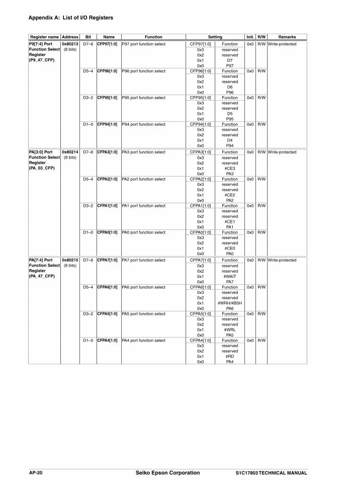
Appendix A: List of I/O Registers
AP-20 Seiko Epson Corporation S1C17803 TECHNICAL MANUAL
Register name Address Bit Name Function Setting Init. R/W Remarks
P9[7:4] Port Function Select Register(P9_47_CFP)
0x80213(8 bits)
D7–6 CFP97[1:0] P97 port function select CFP97[1:0] Function 0x0 R/W Write-protected0x30x20x10x0
reservedreserved
D7P97
D5–4 CFP96[1:0] P96 port function select CFP96[1:0] Function 0x0 R/W0x30x20x10x0
reservedreserved
D6P96
D3–2 CFP95[1:0] P95 port function select CFP95[1:0] Function 0x0 R/W0x30x20x10x0
reservedreserved
D5P95
D1–0 CFP94[1:0] P94 port function select CFP94[1:0] Function 0x0 R/W0x30x20x10x0
reservedreserved
D4P94
PA[3:0] Port Function Select Register(PA_03_CFP)
0x80214(8 bits)
D7–6 CFPA3[1:0] PA3 port function select CFPA3[1:0] Function 0x0 R/W Write-protected0x30x20x10x0
reservedreserved
#CE3PA3
D5–4 CFPA2[1:0] PA2 port function select CFPA2[1:0] Function 0x0 R/W0x30x20x10x0
reservedreserved
#CE2PA2
D3–2 CFPA1[1:0] PA1 port function select CFPA1[1:0] Function 0x0 R/W0x30x20x10x0
reservedreserved
#CE1PA1
D1–0 CFPA0[1:0] PA0 port function select CFPA0[1:0] Function 0x0 R/W0x30x20x10x0
reservedreserved
#CE0PA0
PA[7:4] Port Function Select Register(PA_47_CFP)
0x80215(8 bits)
D7–6 CFPA7[1:0] PA7 port function select CFPA7[1:0] Function 0x0 R/W Write-protected0x30x20x10x0
reservedreserved#WAIT
PA7D5–4 CFPA6[1:0] PA6 port function select CFPA6[1:0] Function 0x0 R/W
0x30x20x10x0
reservedreserved
#WRH/#BSHPA6
D3–2 CFPA5[1:0] PA5 port function select CFPA5[1:0] Function 0x0 R/W0x30x20x10x0
reservedreserved
#WRLPA5
D1–0 CFPA4[1:0] PA4 port function select CFPA4[1:0] Function 0x0 R/W0x30x20x10x0
reservedreserved
#RDPA4

Appendix A: List of I/O Registers
S1C17803 TECHNICAL MANUAL Seiko Epson Corporation AP-21
Register name Address Bit Name Function Setting Init. R/W Remarks
PB[3:0] Port Function Select Register(PB_03_CFP)
0x80216(8 bits)
D7–6 CFPB3[1:0] PB3 port function select CFPB3[1:0] Function 0x0 R/W Write-protected0x30x20x10x0
reservedreserved
D11PB3
D5–4 CFPB2[1:0] PB2 port function select CFPB2[1:0] Function 0x0 R/W0x30x20x10x0
reservedreserved
D10PB2
D3–2 CFPB1[1:0] PB1 port function select CFPB1[1:0] Function 0x0 R/W0x30x20x10x0
reservedreserved
D9PB1
D1–0 CFPB0[1:0] PB0 port function select CFPB0[1:0] Function 0x0 R/W0x30x20x10x0
reservedreserved
D8PB0
PB[7:4] Port Function Select Register(PB_47_CFP)
0x80217(8 bits)
D7–6 CFPB7[1:0] PB7 port function select CFPB7[1:0] Function 0x0 R/W Write-protected0x30x20x10x0
reservedreserved
D15PB7
D5–4 CFPB6[1:0] PB6 port function select CFPB6[1:0] Function 0x0 R/W0x30x20x10x0
reservedreserved
D14PB6
D3–2 CFPB5[1:0] PB5 port function select CFPB5[1:0] Function 0x0 R/W0x30x20x10x0
reservedreserved
D13PB5
D1–0 CFPB4[1:0] PB4 port function select CFPB4[1:0] Function 0x0 R/W0x30x20x10x0
reservedreserved
D12PB4
PC[3:0] Port Function Select Register(PC_03_CFP)
0x80218(8 bits)
D7–6 CFPC3[1:0] PC3 port function select CFPC3[1:0] Function 0x0 R/W Write-protected0x30x20x10x0
reservedFPDAT3
I2S_MCLKPC3
D5–4 CFPC2[1:0] PC2 port function select CFPC2[1:0] Function 0x0 R/W0x30x20x10x0
reservedFPDAT2I2S_SCK
PC2D3–2 CFPC1[1:0] PC1 port function select CFPC1[1:0] Function 0x0 R/W
0x30x20x10x0
reservedFPDAT1I2S_WS
PC1D1–0 CFPC0[1:0] PC0 port function select CFPC0[1:0] Function 0x0 R/W
0x30x20x10x0
reservedFPDAT0I2S_SDO
PC0

Appendix A: List of I/O Registers
AP-22 Seiko Epson Corporation S1C17803 TECHNICAL MANUAL
Register name Address Bit Name Function Setting Init. R/W Remarks
PC[7:4] Port Function Select Register(PC_47_CFP)
0x80219(8 bits)
D7–6 CFPC7[1:0] PC7 port function select CFPC7[1:0] Function 0x0 R/W Write-protected0x30x20x10x0
reservedFPDAT7ATMBPC7
D5–4 CFPC6[1:0] PC6 port function select CFPC6[1:0] Function 0x0 R/W0x30x20x10x0
reservedFPDAT6EXCL0
PC6D3–2 CFPC5[1:0] PC5 port function select CFPC5[1:0] Function 0x0 R/W
0x30x20x10x0
reservedFPDAT5
TMLPC5
D1–0 CFPC4[1:0] PC4 port function select CFPC4[1:0] Function 0x0 R/W0x30x20x10x0
reservedFPDAT4
TMHPC4
P Port Noise Filter Control Register(PP_NFC)
0x8023e(8 bits)
D7–1 – reserved – – – 0 when being read.
D0 ANFEN Input port noise filter enable 1 Enable 0 Disable 0 R/W
Port Function Protect Register(PF_WREN)
0x8023f(8 bits)
D7–0 PFWEN[7:0]
Port function select register protect flag
Writing 10010110 (0x96) removes the write protection of the port function select regis-ters (0x80200–0x80219).Writing another value set the write protection.
0x0 R/W
0x80300 Prescaler Ch.1, Ch.2
Register name Address Bit Name Function Setting Init. R/W Remarks
PSC Ch.1–2 Control Register(PSC_CTL1)
0x80300(8 bits)
D7–2 – reserved – – – 0 when being read.D1 PRUND PSC Ch.1–2 run/stop in debug
mode1 Run 0 Stop 0 R/W
D0 PRUN PSC Ch.1–2 run/stop control 1 Run 0 Stop 0 R/W
0x80500–0x80572 USI Ch.0
Register name Address Bit Name Function Setting Init. R/W Remarks
USI Ch.0 Global Configuration Register (USI_GCFG0)
0x80500(8 bits)
D7–4 – reserved – – – 0 when being read.D3 LSBFST MSB/LSB first mode select 1 MSB first 0 LSB first 0 R/W
D2–0 USIMOD[2:0]
Interface mode configuration USIMOD[2:0] I/F mode 0x0 R/W0x7–0x6
0x50x40x30x20x10x0
reservedI2C slave
I2C masterSPI slave
SPI masterUART
Software reset
USI Ch.0 Transmit Data Buffer Register (USI_TD0)
0x80501(8 bits)
D7–0 TD[7:0] USI transmit data bufferTD7 = MSBTD0 = LSB
0x0 to 0xff 0x0 R/W
USI Ch.0 Receive Data Buffer Register (USI_RD0)
0x80502(8 bits)
D7–0 RD[7:0] USI receive data bufferRD7 = MSBRD0 = LSB
0x0 to 0xff 0x0 R
USI Ch.0 UART Mode Configuration Register (USI_UCFG0)
0x80540(8 bits)
D7–4 – reserved – – – 0 when being read.D3 UCHLN Character length select 1 8 bits 0 7 bits 0 R/WD2 USTPB Stop bit select 1 2 bits 0 1 bit 0 R/WD1 UPMD Parity mode select 1 Even 0 Odd 0 R/WD0 UPREN Parity enable 1 With parity 0 No parity 0 R/W
USI Ch.0 UART Mode Interrupt Enable Register (USI_UIE0)
0x80541(8 bits)
D7–3 – reserved – – – 0 when being read.D2 UEIE Receive error interrupt enable 1 Enable 0 Disable 0 R/WD1 URDIE Receive buffer full interrupt enable 1 Enable 0 Disable 0 R/WD0 UTDIE Transmit buffer empty int. enable 1 Enable 0 Disable 0 R/W
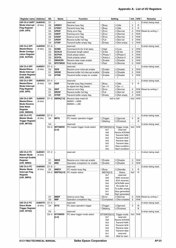
Appendix A: List of I/O Registers
S1C17803 TECHNICAL MANUAL Seiko Epson Corporation AP-23
Register name Address Bit Name Function Setting Init. R/W Remarks
USI Ch.0 UART Mode Interrupt Flag Register (USI_UIF0)
0x80542(8 bits)
D7 – reserved – – – 0 when being read.D6 URBSY Receive busy flag 1 Busy 0 Idle 0 RD5 UTBSY Transmit busy flag 1 Busy 0 Idle 0 RD4 UPEIF Parity error flag 1 Error 0 Normal 0 R/W Reset by writing 1.D3 USEIF Framing error flag 1 Error 0 Normal 0 R/WD2 UOEIF Overrun error flag 1 Error 0 Normal 0 R/WD1 URDIF Receive buffer full flag 1 Full 0 Not full 0 R/WD0 UTDIF Transmit buffer empty flag 1 Empty 0 Not empty 0 R/W
USI Ch.0 SPI Master/Slave Mode Configu-ration Register (USI_SCFG0)
0x80550(8 bits)
D7–6 – reserved – – – 0 when being read.D5 SCMD Command bit (for 9-bit data) 1 High 0 Low 0 R/WD4 SCHLN Character length select 1 9 bits 0 8 bits 0 R/WD3 SCPHA Clock phase select 1 Phase 1 0 Phase 0 0 R/WD2 SCPOL Clock polarity select 1 Active L 0 Active H 0 R/WD1 SMSKEN Receive data mask enable 1 Enable 0 Disable 0 R/WD0 SFSTMOD Fast mode select 1 Fast 0 Normal 0 R/W
USI Ch.0 SPI Master/Slave Mode Interrupt Enable Register (USI_SIE0)
0x80551(8 bits)
D7–3 – reserved – – – 0 when being read.D2 SEIE Receive error interrupt enable 1 Enable 0 Disable 0 R/WD1 SRDIE Receive buffer full interrupt enable 1 Enable 0 Disable 0 R/WD0 STDIE Transmit buffer empty int. enable 1 Enable 0 Disable 0 R/W
USI Ch.0 SPI Master/Slave Mode Interrupt Flag Register (USI_SIF0)
0x80552(8 bits)
D7–4 – reserved – – – 0 when being read.D3 SSIF Transfer busy flag (master) 1 Busy 0 Idle 0 R
ss signal low flag (slave) 1 ss = H 0 ss = LD2 SEIF Overrun error flag 1 Error 0 Normal 0 R/W Reset by writing 1.D1 SRDIF Receive buffer full flag 1 Full 0 Not full 0 R/WD0 STDIF Transmit buffer empty flag 1 Empty 0 Not empty 0 R/W
USI Ch.0 SPI Master/Slave Mode Receive Data Mask Register (USI_SMSK0)
0x8055f(8 bits)
D7–0 SMSK[7:0] Receive data mask bitSMSK7 = MSBSMSK0 = LSB
0x0 to 0xff 0x0 R/W
USI Ch.0 I2C Master Mode Trigger Register (USI_IMTG0)
0x80560(8 bits)
D7–5 – reserved – – – 0 when being read.D4 IMTG I2C master operation trigger 1 Trigger 0 Ignored 0 W
1 Waiting 0 Finished RD3 – reserved – – – 0 when being read.
D2–0 IMTGMOD[2:0]
I2C master trigger mode select IMTGMOD[2:0] Trigger mode 0x0 R/W0x70x60x50x40x30x20x10x0
reservedReceive ACK/NAKTransmit NAKTransmit ACK Receive dataTransmit dataStop conditionStart condition
USI Ch.0 I2C Master Mode Interrupt Enable Register (USI_IMIE0)
0x80561(8 bits)
D7–2 – reserved – – – 0 when being read.
D1 IMEIE Receive error interrupt enable 1 Enable 0 Disable 0 R/WD0 IMIE Operation completion int. enable 1 Enable 0 Disable 0 R/W
USI Ch.0 I2C Master Mode Interrupt Flag Register (USI_IMIF0)
0x80562(8 bits)
D7–6 – reserved – – – 0 when being read.D5 IMBSY I2C master busy flag 1 Busy 0 Standby 0 R
D4–2 IMSTA[2:0] I2C master status IMSTA[2:0] Status 0x0 R0x70x60x50x40x30x20x10x0
reservedNAK receivedACK receivedACK/NAK sentRx buffer full
Tx buffer emptyStop generatedStart generated
D1 IMEIF Overrun error flag 1 Error 0 Normal 0 R/W Reset by writing 1.D0 IMIF Operation completion flag 1 Completed 0 Not completed 0 R/W
USI Ch.0 I2C Slave Mode Trigger Register (USI_ISTG0)
0x80570(8 bits)
D7–5 – reserved – – – 0 when being read.D4 ISTG I2C slave operation trigger 1 Trigger 0 Ignored 0 W
1 Waiting 0 Finished RD3 – reserved – – – 0 when being read.
D2–0 ISTGMOD[2:0]
I2C slave trigger mode select ISTGMOD[2:0] Trigger mode 0x0 R/W0x70x60x50x40x30x20x10x0
reservedReceive ACK/NAKTransmit NAKTransmit ACK Receive dataTransmit data
reservedWait for start

Appendix A: List of I/O Registers
AP-24 Seiko Epson Corporation S1C17803 TECHNICAL MANUAL
Register name Address Bit Name Function Setting Init. R/W Remarks
USI Ch.0 I2C Slave Mode Interrupt Enable Register (USI_ISIE0)
0x80571(8 bits)
D7–2 – reserved – – – 0 when being read.
D1 ISEIE Receive error interrupt enable 1 Enable 0 Disable 0 R/WD0 ISIE Operation completion int. enable 1 Enable 0 Disable 0 R/W
USI Ch.0 I2C Slave Mode Interrupt Flag Register (USI_ISIF0)
0x80572(8 bits)
D7–6 – reserved – – – 0 when being read.D5 ISBSY I2C slave busy flag 1 Busy 0 Standby 0 R
D4–2 ISSTA[2:0] I2C slave status ISSTA[2:0] Status 0x0 R0x70x60x50x40x30x20x10x0
reservedNAK receivedACK receivedACK/NAK sentRx buffer full
Tx buffer emptyStop detectedStart detected
D1 ISEIF Overrun error flag 1 Error 0 Normal 0 R/W Reset by writing 1.D0 ISIF Operation completion flag 1 Completed 0 Not completed 0 R/W
0x80600–0x80672 USI Ch.1
Register name Address Bit Name Function Setting Init. R/W Remarks
USI Ch.1 Global Configuration Register (USI_GCFG1)
0x80600(8 bits)
D7–4 – reserved – – – 0 when being read.D3 LSBFST MSB/LSB first mode select 1 MSB first 0 LSB first 0 R/W
D2–0 USIMOD[2:0]
Interface mode configuration USIMOD[2:0] I/F mode 0x0 R/W0x7–0x6
0x50x40x30x20x10x0
reservedI2C slave
I2C masterSPI slave
SPI masterUART
Software reset
USI Ch.1 Transmit Data Buffer Register (USI_TD1)
0x80601(8 bits)
D7–0 TD[7:0] USI transmit data bufferTD7 = MSBTD0 = LSB
0x0 to 0xff 0x0 R/W
USI Ch.1 Receive Data Buffer Register (USI_RD1)
0x80602(8 bits)
D7–0 RD[7:0] USI receive data bufferRD7 = MSBRD0 = LSB
0x0 to 0xff 0x0 R
USI Ch.1 UART Mode Configuration Register (USI_UCFG1)
0x80640(8 bits)
D7–4 – reserved – – – 0 when being read.D3 UCHLN Character length select 1 8 bits 0 7 bits 0 R/WD2 USTPB Stop bit select 1 2 bits 0 1 bit 0 R/WD1 UPMD Parity mode select 1 Even 0 Odd 0 R/WD0 UPREN Parity enable 1 With parity 0 No parity 0 R/W
USI Ch.1 UART Mode Interrupt Enable Register (USI_UIE1)
0x80641(8 bits)
D7–3 – reserved – – – 0 when being read.D2 UEIE Receive error interrupt enable 1 Enable 0 Disable 0 R/WD1 URDIE Receive buffer full interrupt enable 1 Enable 0 Disable 0 R/WD0 UTDIE Transmit buffer empty int. enable 1 Enable 0 Disable 0 R/W
USI Ch.1 UART Mode Interrupt Flag Register (USI_UIF1)
0x80642(8 bits)
D7 – reserved – – – 0 when being read.D6 URBSY Receive busy flag 1 Busy 0 Idle 0 RD5 UTBSY Transmit busy flag 1 Busy 0 Idle 0 RD4 UPEIF Parity error flag 1 Error 0 Normal 0 R/W Reset by writing 1.D3 USEIF Framing error flag 1 Error 0 Normal 0 R/WD2 UOEIF Overrun error flag 1 Error 0 Normal 0 R/WD1 URDIF Receive buffer full flag 1 Full 0 Not full 0 R/WD0 UTDIF Transmit buffer empty flag 1 Empty 0 Not empty 0 R/W
USI Ch.1 SPI Master/Slave Mode Configu-ration Register (USI_SCFG1)
0x80650(8 bits)
D7–6 – reserved – – – 0 when being read.D5 SCMD Command bit (for 9-bit data) 1 High 0 Low 0 R/WD4 SCHLN Character length select 1 9 bits 0 8 bits 0 R/WD3 SCPHA Clock phase select 1 Phase 1 0 Phase 0 0 R/WD2 SCPOL Clock polarity select 1 Active L 0 Active H 0 R/WD1 SMSKEN Receive data mask enable 1 Enable 0 Disable 0 R/WD0 SFSTMOD Fast mode select 1 Fast 0 Normal 0 R/W
USI Ch.1 SPI Master/Slave Mode Interrupt Enable Register (USI_SIE1)
0x80651(8 bits)
D7–3 – reserved – – – 0 when being read.D2 SEIE Receive error interrupt enable 1 Enable 0 Disable 0 R/WD1 SRDIE Receive buffer full interrupt enable 1 Enable 0 Disable 0 R/WD0 STDIE Transmit buffer empty int. enable 1 Enable 0 Disable 0 R/W

Appendix A: List of I/O Registers
S1C17803 TECHNICAL MANUAL Seiko Epson Corporation AP-25
Register name Address Bit Name Function Setting Init. R/W Remarks
USI Ch.1 SPI Master/Slave Mode Interrupt Flag Register (USI_SIF1)
0x80652(8 bits)
D7–4 – reserved – – – 0 when being read.D3 SSIF Transfer busy flag (master) 1 Busy 0 Idle 0 R
ss signal low flag (slave) 1 ss = H 0 ss = LD2 SEIF Overrun error flag 1 Error 0 Normal 0 R/W Reset by writing 1.D1 SRDIF Receive buffer full flag 1 Full 0 Not full 0 R/WD0 STDIF Transmit buffer empty flag 1 Empty 0 Not empty 0 R/W
USI Ch.1 SPI Master/Slave Mode Receive Data Mask Register (USI_SMSK1)
0x8065f(8 bits)
D7–0 SMSK[7:0] Receive data mask bitSMSK7 = MSBSMSK0 = LSB
0x0 to 0xff 0x0 R/W
USI Ch.1 I2C Master Mode Trigger Register (USI_IMTG1)
0x80660(8 bits)
D7–5 – reserved – – – 0 when being read.D4 IMTG I2C master operation trigger 1 Trigger 0 Ignored 0 W
1 Waiting 0 Finished RD3 – reserved – – – 0 when being read.
D2–0 IMTGMOD[2:0]
I2C master trigger mode select IMTGMOD[2:0] Trigger mode 0x0 R/W0x70x60x50x40x30x20x10x0
reservedReceive ACK/NAKTransmit NAKTransmit ACK Receive dataTransmit dataStop conditionStart condition
USI Ch.1 I2C Master Mode Interrupt Enable Register (USI_IMIE1)
0x80661(8 bits)
D7–2 – reserved – – – 0 when being read.
D1 IMEIE Receive error interrupt enable 1 Enable 0 Disable 0 R/WD0 IMIE Operation completion int. enable 1 Enable 0 Disable 0 R/W
USI Ch.1 I2C Master Mode Interrupt Flag Register (USI_IMIF1)
0x80662(8 bits)
D7–6 – reserved – – – 0 when being read.D5 IMBSY I2C master busy flag 1 Busy 0 Standby 0 R
D4–2 IMSTA[2:0] I2C master status IMSTA[2:0] Status 0x0 R0x70x60x50x40x30x20x10x0
reservedNAK receivedACK receivedACK/NAK sentRx buffer full
Tx buffer emptyStop generatedStart generated
D1 IMEIF Overrun error flag 1 Error 0 Normal 0 R/W Reset by writing 1.D0 IMIF Operation completion flag 1 Completed 0 Not completed 0 R/W
USI Ch.1 I2C Slave Mode Trigger Register (USI_ISTG1)
0x80670(8 bits)
D7–5 – reserved – – – 0 when being read.D4 ISTG I2C slave operation trigger 1 Trigger 0 Ignored 0 W
1 Waiting 0 Finished RD3 – reserved – – – 0 when being read.
D2–0 ISTGMOD[2:0]
I2C slave trigger mode select ISTGMOD[2:0] Trigger mode 0x0 R/W0x70x60x50x40x30x20x10x0
reservedReceive ACK/NAKTransmit NAKTransmit ACK Receive dataTransmit data
reservedWait for start
USI Ch.1 I2C Slave Mode Interrupt Enable Register (USI_ISIE1)
0x80671(8 bits)
D7–2 – reserved – – – 0 when being read.
D1 ISEIE Receive error interrupt enable 1 Enable 0 Disable 0 R/WD0 ISIE Operation completion int. enable 1 Enable 0 Disable 0 R/W
USI Ch.1 I2C Slave Mode Interrupt Flag Register (USI_ISIF1)
0x80672(8 bits)
D7–6 – reserved – – – 0 when being read.D5 ISBSY I2C slave busy flag 1 Busy 0 Standby 0 R
D4–2 ISSTA[2:0] I2C slave status ISSTA[2:0] Status 0x0 R0x70x60x50x40x30x20x10x0
reservedNAK receivedACK receivedACK/NAK sentRx buffer full
Tx buffer emptyStop detectedStart detected
D1 ISEIF Overrun error flag 1 Error 0 Normal 0 R/W Reset by writing 1.D0 ISIF Operation completion flag 1 Completed 0 Not completed 0 R/W

Appendix A: List of I/O Registers
AP-26 Seiko Epson Corporation S1C17803 TECHNICAL MANUAL
0x80800–0x8080f Real-Time Clock
Register name Address Bit Name Function Setting Init. R/W Remarks
RTC Interrupt Status Register(RTC_INTSTAT)
0x80800(8 bits)
D7–1 – reserved – – – 0 when being read.D0 RTCIRQ Interrupt status 1 Occurred 0 Not occurred X (0) R/W Reset by writing 1.
RTC Interrupt Mode Register(RTC_INTMODE)
0x80801(8 bits)
D7–4 – reserved – – – 0 when being read.D3–2 RTCT[1:0] RTC interrupt cycle setup RTCT[1:0] Cycle X
(0x1)R/W
0x30x20x10x0
1 hour1 minute1 second
1/64 secondD1 RTCIMD reserved 1 X (1) R/W Always set to 1.D0 RTCIEN RTC interrupt enable 1 Enable 0 Disable X (0) R/W
RTC Control 0 Register(RTC_CNTL0)
0x80802(8 bits)
D7–5 – reserved – – – 0 when being read.D4 RTC24H 24H mode select 1 24H 0 reserved
(use prohib-ited)
X (0) R/W Always set to 1.
D3 – reserved – – – 0 when being read.D2 RTCADJ 30-second adjustment 1 Adjust 0 – X (0) R/WD1 RTCSTP Divider run/stop control 1 Stop 0 Run X (0) R/WD0 RTCRST Software reset 1 Reset 0 – X (X) R/W
RTC Control 1 Register(RTC_CNTL1)
0x80803(8 bits)
D7–2 – reserved – – – 0 when being read.D1 RTCBSY Counter busy flag 1 Busy 0 R/W possible X (0) RD0 RTCHLD Counter hold control 1 Hold 0 Running X (0) R/W
RTC Second Register(RTC_SEC)
0x80804(8 bits)
D7 – reserved – – – 0 when being read.D6–4 RTCSH[2:0] RTC 10-second counter 0 to 5 X (*) R/WD3–0 RTCSL[3:0] RTC 1-second counter 0 to 9 X (*) R/W
RTC Minute Register(RTC_MIN)
0x80805(8 bits)
D7 – reserved – – – 0 when being read.D6–4 RTCMIH[2:0] RTC 10-minute counter 0 to 5 X (*) R/WD3–0 RTCMIL[3:0] RTC 1-minute counter 0 to 9 X (*) R/W
RTC Hour Register(RTC_HOUR)
0x80806(8 bits)
D7–6 – reserved – – – 0 when being read.D5–4 RTCHH[1:0] RTC 10-hour counter 0 to 2 X (*) R/WD3–0 RTCHL[3:0] RTC 1-hour counter 0–9 X (*) R/W
RTC Day Register(RTC_DAY)
0x80807(8 bits)
D7–6 – reserved – – – 0 when being read.D5–4 RTCDH[1:0] RTC 10-day counter 0 to 3 X (*) R/WD3–0 RTCDL[3:0] RTC 1-day counter 0 to 9 X (*) R/W
RTC Month Register(RTC_MONTH)
0x80808(8 bits)
D7–5 – reserved – – – 0 when being read.D4 RTCMOH RTC 10-month counter 0 to 1 X (*) R/W
D3–0 RTCMOL[3:0] RTC 1-month counter 0 to 9 X (*) R/W
RTC Year Register(RTC_YEAR)
0x80809(8 bits)
D7–4 RTCYH[3:0] RTC 10-year counter 0 to 9 X (*) R/WD3–0 RTCYL[3:0] RTC 1-year counter 0 to 9 X (*) R/W
RTC Days of Week Register(RTC_WEEK)
0x8080a(8 bits)
D7–3 – reserved – – – 0 when being read.D2–0 RTCWK[2:0] RTC days of week counter RTCWK[2:0] Days of week X (*) R/W
0x70x60x50x40x30x20x10x0
–Saturday
FridayThursday
WednesdayTuesdayMondaySunday
RTC Wakeup Configuration Register(RTC_WAKEUP)
0x8080f(8 bits)
D7–2 – reserved – – – 0 when being read.
D1 WUP_CTL WAKEUP control 1 Active 0 Inactive X (0) R/WD0 WUP_POL WAKEUP polarity select 1 Active low 0 Active high X (0) R/W
Init.: ( ) indicates the value set after a software reset (RTCRST → 1 → 0) is performed.* Software reset (RTCRST → 1 → 0) does not affect the counter values. This register retains the value set before a software reset is
performed.
0x80900–0x8090f BBRAM
Register name Address Bit Name Function Setting Init. R/W Remarks
BBRAM0 |BBRAM15
0x80900|
0x8090f(8 bits)
D7–0 BBRAMD[7:0]
BBRAM data 0x0 to 0xff X R/W
RTC Wait Control Register(RTC_WAIT)
0x80910(8 bits)
D7–3 – reserved – – – 0 when being read.D2–0 RTC_WAIT
[2:0]RTC access wait cycle setup RTC_WAIT[2:0] Wait cycle 0x7 R/W
0x7:
0x0
7 cycles:
0 cycles

Appendix A: List of I/O Registers
S1C17803 TECHNICAL MANUAL Seiko Epson Corporation AP-27
0x81060–0x8106c Watchdog Timer
Register name Address Bit Name Function Setting Init. R/W Remarks
WDT Write Protect Register(WD_WP)
0x81060(16 bits)
D15–0 WDPTC[15:0]
WDT register write protect flag Writing 0x96 removes the write protection of the WD_EN, WD_CMP_L, and WD_CMP_H registers.Writing another value set the write protection.
X W 0 when being read.
WDT Enable and Setup Register(WD_EN)
0x81062(16 bits)
D15–7 – reserved – – – 0 when being read.D6 CLKSEL WDT input clock select 1 External clk 0 Internal clk 0 R/W Write-protectedD5 CLKEN WDT clock output control 1 On 0 Off 0 R/WD4 RUNSTP WDT Run/Stop control 1 Run 0 Stop 0 R/W
D3–2 – reserved – – – 0 when being read.D1 NMIEN WDT NMI enable 1 Enable 0 Disable 0 R/W Write-protectedD0 RESEN WDT RESET enable 1 Enable 0 Disable 0 R/W
WDT Comparison Data L Register (WD_CMP_L)
0x81064(16 bits)
D15–0 CMPDT[15:0]
WDT comparison dataCMPDT0 = LSB
0x0 to 0x3fffffff(low-order 16 bits)
0x0 R/W Write-protected
WDT Comparison Data H Register (WD_CMP_H)
0x81066(16 bits)
D15–14 – reserved – – – 0 when being read.D13-0 CMPDT
[29:16]WDT comparison dataCMPDT29 = MSB
0x0 to 0x3fffffff(high-order 14 bits)
0x0 R/W Write-protected
WDT Count Data L Register (WD_CNT_L)
0x81068(16 bits)
D15–0 CTRDT[15:0]
WDT counter dataCTRDT0 = LSB
0x0 to 0x3fffffff(low-order 16 bits)
X R
WDT Count Data H Register (WD_CNT_H)
0x8106a(16 bits)
D15–14 – reserved – – – 0 when being read.D13-0 CTRDT
[29:16]WDT counter dataCTRDT29 = MSB
0x0 to 0x3fffffff(high-order 14 bits)
X R
WDT Control Register(WD_CTL)
0x8106c(16 bits)
D15–1 – reserved – – – 0 when being read.
D0 WDRESEN WDT reset 1 Reset 0 ignored 0 W
0x81100–0x81106 A/D Converter
Register name Address Bit Name Function Setting Init. R/W Remarks
A/D Conversion Result Register(ADC10_ADD)
0x81100(16 bits)
D15–0 ADD[15:0] A/D converted dataADD[9:0] are effective when STMD = 0 (ADD[15:10] = 0)ADD[15:6] are effective when STMD = 1 (ADD[5:0] = 0)
0x0 to 0x3ff 0x0 R
A/D Trigger/ Channel Select Register(ADC10_TRG)
0x81102(16 bits)
D15–14 – reserved – – – 0 when being read.D13–11 ADCE[2:0] End channel select 0x0 to 0x3 0x0 R/WD10–8 ADCS[2:0] Start channel select 0x0 to 0x3 0x0 R/W
D7 STMD Conversion result storing mode 1 ADD[15:6] 0 ADD[9:0] 0 R/WD6 ADMS Conversion mode select 1 Continuous 0 Single 0 R/W
D5–4 ADTS[1:0] Conversion trigger select ADTS[1:0] Trigger 0x0 R/W0x30x20x10x0
#ADTRG pinreservedT8F Ch.2Software
D3 – reserved – – – 0 when being read.D2–0 ADST[2:0] Sampling time setting ADST[2:0] Sampling time 0x7 R/W
0x70x60x50x40x30x20x10x0
9•ADCCLK8•ADCCLK7•ADCCLK6•ADCCLK5•ADCCLK4•ADCCLK3•ADCCLK2•ADCCLK
A/D Control/ Status Register(ADC10_CTL)
0x81104(16 bits)
D15 – reserved – – – 0 when being read.D14–12 ADICH[2:0] Conversion channel indicator 0x0 to 0x3 0x0 R
D11 – reserved – – – 0 when being read.D10 ADIBS ADC10 status 1 Busy 0 Idle 0 RD9 ADOWE Overwrite error flag 1 Error 0 Normal 0 R/W Reset by writing 1.D8 ADCF Conversion completion flag 1 Completed 0 Run/Stand-
by0 R Reset when ADC10_
ADD is read.D7–6 – reserved – – – 0 when being read.
D5 ADOIE Overwrite error interrupt enable 1 Enable 0 Disable 0 R/WD4 ADCIE Conversion completion int. enable 1 Enable 0 Disable 0 R/W
D3–2 – reserved – – – 0 when being read.D1 ADCTL A/D conversion control 1 Start 0 Stop 0 R/WD0 ADEN ADC10 enable 1 Enable 0 Disable 0 R/W

Appendix A: List of I/O Registers
AP-28 Seiko Epson Corporation S1C17803 TECHNICAL MANUAL
Register name Address Bit Name Function Setting Init. R/W Remarks
A/D Clock Control Register(ADC10_CLK)
0x81106(16 bits)
D15–4 – reserved – – – 0 when being read.D3–0 ADDF[3:0] A/D converter clock division ratio
selectADDF[3:0] A/D clock 0x0 R/W
0xf0xe0xd0xc0xb0xa0x90x80x70x60x50x40x30x20x10x0
reservedPCLK2•1/32768PCLK2•1/16384PCLK2•1/8192PCLK2•1/4096PCLK2•1/2048PCLK2•1/1024PCLK2•1/512PCLK2•1/256PCLK2•1/128PCLK2•1/64PCLK2•1/32PCLK2•1/16PCLK2•1/8PCLK2•1/4PCLK2•1/2
0x81200–0x81206 Remote Controller
Register name Address Bit Name Function Setting Init. R/W Remarks
REMC Configuration Register(REMC_CFG)
0x81200(16 bits)
D15–12 CGCLK[3:0] Carrier generator clock select(Prescaler output clock)
CGCLK[3:0]LCCLK[3:0]
Clock0x0 R/W
0xf0xe0xd0xc0xb0xa0x90x80x70x60x50x40x30x20x10x0
reservedPCLK2•1/16384PCLK2•1/8192PCLK2•1/4096PCLK2•1/2048PCLK2•1/1024PCLK2•1/512PCLK2•1/256PCLK2•1/128PCLK2•1/64PCLK2•1/32PCLK2•1/16PCLK2•1/8PCLK2•1/4PCLK2•1/2PCLK2•1/1
D11–8 LCCLK[3:0] Length counter clock select(Prescaler output clock)
0x0 R/W
D7–2 – reserved – – – 0 when being read.D1 REMMD REMC mode select 1 Receive 0 Transmit 0 R/WD0 REMEN REMC enable 1 Enable 0 Disable 0 R/W
REMC Carrier Length Setup Register(REMC_CAR)
0x81202(16 bits)
D15–14 – reserved – – – 0 when being read.D13–8 REMCL[5:0] Carrier L length setup 0x0 to 0x3f 0x0 R/WD7–6 – reserved – – – 0 when being read.D5–0 REMCH[5:0] Carrier H length setup 0x0 to 0x3f 0x0 R/W
REMC Length Counter Register(REMC_LCNT)
0x81204(16 bits)
D15–8 REMLEN[7:0] Transmit/receive data length count(down counter)
0x0 to 0xff 0x0 R/W
D7–1 – reserved – – – 0 when being read.D0 REMDT Transmit/receive data 1 1 (H) 0 0 (L) 0 R/W
REMC Interrupt Control Register(REMC_INT)
0x81206(16 bits)
D15–11 – reserved – – – 0 when being read.D10 REMFIF Falling edge interrupt flag 1 Cause of
interrupt occurred
0 Cause of interrupt not occurred
0 R/W Reset by writing 1.D9 REMRIF Rising edge interrupt flag 0 R/WD8 REMUIF Underflow interrupt flag 0 R/W
D7–3 – reserved – – – 0 when being read.D2 REMFIE Falling edge interrupt enable 1 Enable 0 Disable 0 R/WD1 REMRIE Rising edge interrupt enable 1 Enable 0 Disable 0 R/WD0 REMUIE Underflow interrupt enable 1 Enable 0 Disable 0 R/W

Appendix A: List of I/O Registers
S1C17803 TECHNICAL MANUAL Seiko Epson Corporation AP-29
0x81300–0x8130c 16-bit PWM Timer
Register name Address Bit Name Function Setting Init. R/W Remarks
T16A Counter Control Register(T16A_CTL)
0x81300(16 bits)
D15–12 – reserved – – – 0 when being read.D11–8 CLKS[3:0] Counter clock select CLKS[3:0] Clock 0x0 R/W
0xf0xe0xd0xc0xb0xa0x90x80x70x60x50x40x30x20x10x0
External clockPCLK1•1/16384PCLK1•1/8192PCLK1•1/4096PCLK1•1/2048PCLK1•1/1024PCLK1•1/512PCLK1•1/256PCLK1•1/128PCLK1•1/64PCLK1•1/32PCLK1•1/16PCLK1•1/8PCLK1•1/4PCLK1•1/2PCLK1•1/1
D7–4 – reserved – – – 0 when being read.D3 CBUFEN Compare buffer enable 1 Enable 0 Disable 0 R/WD2 TMMD Count mode select 1 One-shot 0 Repeat 0 R/WD1 PRESET Counter reset 1 Reset 0 Ignored 0 W 0 when being read.D0 PRUN Counter run/stop control 1 Run 0 Stop 0 R/W
T16A Counter Data Register(T16A_TC)
0x81302(16 bits)
D15–0 T16ATC[15:0]
Counter dataT16ATC15 = MSBT16ATC0 = LSB
0x0 to 0xffff 0x0 R
T16A Comparator/Capture Control Register(T16A_CCCTL)
0x81304(16 bits)
D15–14 CAPBTRG[1:0]
Capture B trigger select CAPBTRG[1:0] Trigger edge 0x0 R/W0x30x20x10x0
↑ and ↓↓↑
NoneD13–12 TOUTBMD
[1:0]TOUT B mode select TOUTBMD[1:0] Mode 0x0 R/W
0x30x20x10x0
cmp B: ↑ or ↓cmp A: ↑ or ↓cmp A: ↑, B: ↓
OffD11–10 – reserved – – – 0 when being read.
D9 TOUTBINV TOUT B invert 1 Invert 0 Normal 0 R/WD8 CCBMD T16A_CCB register mode select 1 Capture 0 Comparator 0 R/W
D7–6 CAPATRG[1:0]
Capture A trigger select CAPATRG[1:0] Trigger edge 0x0 R/W0x30x20x10x0
↑ and ↓↓↑
NoneD5–4 TOUTAMD
[1:0]TOUT A mode select TOUTAMD[1:0] Mode 0x0 R/W
0x30x20x10x0
cmp B: ↑ or ↓cmp A: ↑ or ↓cmp A: ↑, B: ↓
OffD3–2 – reserved – – – 0 when being read.
D1 TOUTAINV TOUT A invert 1 Invert 0 Normal 0 R/WD0 CCAMD T16A_CCA register mode select 1 Capture 0 Comparator 0 R/W
T16A Comparator/Capture A Data Register(T16A_CCA)
0x81306(16 bits)
D15–0 CCA[15:0] Compare/capture A dataCCA15 = MSBCCA0 = LSB
0x0 to 0xffff 0x0 R/W
T16A Comparator/Capture B Data Register(T16A_CCB)
0x81308(16 bits)
D15–0 CCB[15:0] Compare/capture B dataCCB15 = MSBCCB0 = LSB
0x0 to 0xffff 0x0 R/W
T16A Comparator/Capture Interrupt Enable Register(T16A_IEN)
0x8130a(16 bits)
D15–6 – reserved – – – 0 when being read.D5 CAPBOWIE Capture B overwrite interrupt enable 1 Enable 0 Disable 0 R/WD4 CAPAOWIE Capture A overwrite interrupt enable 1 Enable 0 Disable 0 R/WD3 CAPBIE Capture B interrupt enable 1 Enable 0 Disable 0 R/WD2 CAPAIE Capture A interrupt enable 1 Enable 0 Disable 0 R/WD1 CBIE Compare B interrupt enable 1 Enable 0 Disable 0 R/WD0 CAIE Compare A interrupt enable 1 Enable 0 Disable 0 R/W
T16A Comparator/Capture Interrupt Flag Register(T16A_IFLG)
0x8130c(16 bits)
D15–6 – reserved – – – 0 when being read.D5 CAPBOWIF Capture B overwrite interrupt flag 1 Cause of
interrupt occurred
0 Cause of interrupt not occurred
0 R/W Reset by writing 1.D4 CAPAOWIF Capture A overwrite interrupt flag 0 R/WD3 CAPBIF Capture B interrupt flag 0 R/WD2 CAPAIF Capture A interrupt flag 0 R/WD1 CBIF Compare B interrupt flag 0 R/WD0 CAIF Compare A interrupt flag 0 R/W

Appendix A: List of I/O Registers
AP-30 Seiko Epson Corporation S1C17803 TECHNICAL MANUAL
0x81400–0x8140e 16-bit Audio PWM Timer
Register name Address Bit Name Function Setting Init. R/W Remarks
T16P Compare A Buffer Register(T16P_A)
0x81400(16 bits)
D15–0 CMPA[15:0] Compare A dataCMPA15 = MSBCMPA0 = LSB
0x0 to 0xffff X R/W
T16P Compare B Buffer Register(T16P_B)
0x81402(16 bits)
D15–0 CMPB[15:0] Compare B dataCMPB15 = MSBCMPB0 = LSB
0x0 to 0xffff X R/W
T16P Counter Data Register(T16P_CNT_DATA)
0x81404(16 bits)
D15–0 CNT_DATA[15:0]
Counter dataCNT_DATA15 = MSBCNT_DATA0 = LSB
0x0 to 0xffff X R/W
T16P Volume Control Register(T16P_VOL_CTL)
0x81406(16 bits)
D15–8 – reserved – – – 0 when being read.D7 VOLBPS Volume control enable 1 Disable 0 Enable 1 R/W Effective only for 16-
bit dataD6–0 VOLSEL[6:0]
Volume level select VOLSEL[6:0] Volume level 0x40 R/W0x7f0x7e
:0x40
:0x20x10x0
× 127/64× 126/64
:× 64/64
:× 2/64× 1/64
× 0 (mute)
T16P Control Register(T16P_CTL)
0x81408(16 bits)
D15–12 BCNT[3:0] B match count 0x0 to 0xf 0x0 R/WD11 RESSEL PCM data resolution select 1 16 bits 0 8 bits 1 R/WD10 SGNSEL PCM data format select 1 Signed 0 Unsigned 1 R/WD9–8 SPLTMD
[1:0]Split mode select SPLTMD[1:0] Split mode 0x0 R/W Effective only for 16-
bit data0x30x20x10x0
10 bits + 6 bits9 bits + 7 bits8 bits + 8 bits
Normal (16 bits)D7 – reserved – – – 0 when being read.D6 SELFM Fine mode select 1 Fine mode 0 Normal 0 R/WD5 – reserved – – – 0 when being read.D4 INITOL Initial output level select 1 High 0 Low 0 R/WD3 CLKSEL Input clock select 1 External 0 Internal 0 R/WD2 – reserved – – – 0 when being read.D1 PRESET T16P reset 1 Reset 0 Ignored 0 WD0 – reserved – – –
T16P Running Control Register(T16P_RUN)
0x8140a(16 bits)
D15–1 – reserved – – – 0 when being read.
D0 PRUN T16P run/stop control 1 Run 0 Stop 0 R/W
T16P Internal Clock Control Register(T16P_CLK)
0x8140c(16 bits)
D15–4 – reserved – – – 0 when being read.D3–0 CLKDIV
[3:0]Clock division ratio selection(Prescaler output clock)
CLKDIV[3:0] Count clock 0x0 R/W0xf–0xd
0xc0xb0xa0x90x80x70x60x50x40x30x20x10x0
reservedPCLK1•1/4096PCLK1•1/2048PCLK1•1/1024PCLK1•1/512PCLK1•1/256PCLK1•1/128PCLK1•1/64PCLK1•1/32PCLK1•1/16PCLK1•1/8PCLK1•1/4PCLK1•1/2PCLK1•1/1
T16P Interrupt Control Register(T16P_INT)
0x8140e(16 bits)
D15–11 – reserved – – – 0 when being read.D10 BUFEF Buffer empty interrupt flag 1 Cause of
interrupt occurred
0 Cause of interrupt not occurred
X R/W Reset by writing 1.D9 INTBF B match interrupt flag 0 R/WD8 INTAF A match interrupt flag 0 R/W
D7–3 – reserved – – – 0 when being read.D2 INTBEEN Buffer empty interrupt enable 1 Enable 0 Disable 0 R/WD1 INTBEN B match interrupt enable 1 Enable 0 Disable 0 R/WD0 INTAEN A match interrupt enable 1 Enable 0 Disable 0 R/W

Appendix A: List of I/O Registers
S1C17803 TECHNICAL MANUAL Seiko Epson Corporation AP-31
0x81500–0x81512 I2S
Register name Address Bit Name Function Setting Init. R/W Remarks
I2S Control Register (I2S_CTL)
0x81500(16 bits)
D15–9 – reserved – – – 0 when being read.D8 DTSIGN I2S signed/unsigned data format
select1 Signed 0 Unsigned 0 R/W
D7 WCLKMD I2S output word clock mode select 1 L: HighR: Low
0 L: LowR: High
0 R/W
D6 BCLKPOL I2S output bit clock polarity select 1 Negative 0 Positive 0 R/WD5 DTFORM I2S output data format select 1 LSB first 0 MSB first 0 R/WD4 I2SOUTEN I2S output enable 1 Enable 0 Disable 0 R/W
D3–2 DTTMG[1:0] I2S output data timing select DTTMG[1:0] Timing mode 0x0 R/W0x30x20x10x0
reservedRight justifiedLeft justified
I2SD1–0 CHMD[1:0] I2S output channel mode select CHMD[1:0] Channel mode 0x0 R/W
0x30x20x10x0
MuteMono left
Mono rightStereo
I2S Master Clock Division Ratio Register (I2S_DV_MCLK)
0x81504(16 bits)
D15–6 – reserved – – – 0 when being read.D5–0 MCLKDIV
[5:0]I2S_MCLK division ratio select MCLKDIV[5:0] I2S_MCLK 0x0 R/W
0x3f0x3e0x3d
:0x20x10x0
PCLK1•1/64PCLK1•1/63PCLK1•1/62
:PCLK1•1/3PCLK1•1/2PCLK1•1/1
I2S Audio Clock Division Ratio Register (I2S_DV_AUDIO_CLK)
0x81506(16 bits)
D15–13 – reserved – – – 0 when being read.D12–8 WSCLKCYC
[4:0]I2S WS clock cycle setup WSCLKCYC[4:0] Clock period 0x0 R/W
0x1f–0x110x100xf0xe0xd0xc0xb0xa0x90x80x70x60x50x40x30x20x10x0
reserved32 clocks31 clocks30 clocks29 clocks28 clocks27 clocks26 clocks25 clocks24 clocks23 clocks22 clocks21 clocks20 clocks19 clocks18 clocks17 clocks16 clocks
D7–0 BCLKDIV[7:0]
I2S bit clock division ratio select BCLKDIV[7:0] Bit clock 0x0 R/W0xff0xfe0xfd
:0x20x10x0
PCLK1•1/512PCLK1•1/510PCLK1•1/508
:PCLK1•1/6PCLK1•1/4PCLK1•1/2
I2S Start/Stop Register (I2S_START)
0x81508(16 bits)
D15–8 – reserved – – – 0 when being read.D7 I2SBUSY I2S busy flag 1 Busy 0 Idle 0 R
D6–1 – reserved – – – 0 when being read.D0 I2SSTART I2S start/stop control 1 Start (run) 0 Stop 0 R/W
I2S FIFO Status Register (I2S_FIFO_STAT)
0x8150a(16 bits)
D15–5 – reserved – – – 0 when being read.D4–2 FIFOSTAT
[2:0]I2S FIFO state machine FIFOSTAT[2:0] State 0x0 R
0x7–0x60x50x40x30x20x10x0
reservedFLUSHEMPTYLACKFULLINIT
STOPD1 I2SFIFOFF I2S FIFO full flag 1 Full 0 Not full 0 RD0 I2SFIFOEF I2S FIFO empty flag 1 Empty 0 Not empty 1 R
I2S Interrupt Control Register (I2S_INT)
0x8150c(16 bits)
D15–11 – reserved – – – 0 when being read.D10 WEIF I2S FIFO whole empty int. flag 1 Cause of
interrupt occurred
0 Cause of interrupt not occurred
0 R/W Reset by writing 1.D9 HEIF I2S FIFO half empty interrupt flag 1 0 0 R/WD8 OEIF I2S FIFO one empty interrupt flag 1 0 0 R/W
D7–3 – reserved – – – 0 when being read.D2 WEIE I2S FIFO whole empty int. enable 1 Enable 0 Disable 0 R/WD1 HEIE I2S FIFO half empty int. enable 1 Enable 0 Disable 0 R/WD0 OEIE I2S FIFO one empty int. enable 1 Enable 0 Disable 0 R/W

Appendix A: List of I/O Registers
AP-32 Seiko Epson Corporation S1C17803 TECHNICAL MANUAL
Register name Address Bit Name Function Setting Init. R/W Remarks
I2S FIFO Register (I2S_FIFO)
0x81510(16 bits)
D15–0 I2SFIFO[15:0]
I2S FIFO (L-channel output data) 0 to 0xffff 0x0 W 0 when being read.
0x81512(16 bits)
D15–0 I2S FIFO (R-channel output data)
0x81600–0x81610 SRAM Controller
Register name Address Bit Name Function Setting Init. R/W Remarks
SRAMC Wait Cycle ConfigurationRegister(SRAMC_WT)
0x81600(16 bits)
D15–12 CE3_WT[3:0]
#CE3 static wait cycle configuration
CEx_WT[3:0] Wait cycle 0xf R/W0xf0xe0xd
:0x20x10x0
15 cycles14 cycles13 cycles
:2 cycles1 cycle0 cycles
D11–8 CE2_WT[3:0]
#CE2 static wait cycle configuration
0xf R/W
D7–4 CE1_WT[3:0]
#CE1 static wait cycle configuration
0xf R/W
D3–0 CE0_WT[3:0]
#CE0 static wait cycle configuration
0xf R/W
SRAMC Device Size Configuration Register(SRAMC_SIZE)
0x81604(16 bits)
D15–4 – reserved – – – 0 when being read.D3 CE3_SZ #CE3 device size configuration 1 16 bits 0 8 bits 0 R/WD2 CE2_SZ #CE2 device size configuration 1 16 bits 0 8 bits 0 R/WD1 CE1_SZ #CE1 device size configuration 1 16 bits 0 8 bits 0 R/WD0 CE0_SZ #CE0 device size configuration 1 16 bits 0 8 bits 0 R/W
SRAMCDevice Mode Configuration Register(SRAMC_MOD)
0x81608(16 bits)
D15–4 – reserved – – – 0 when being read.D3 CE3_MOD #CE3 device mode configuration 1 BSL 0 A0 0 R/WD2 CE2_MOD #CE2 device mode configuration 1 BSL 0 A0 0 R/WD1 CE1_MOD #CE1 device mode configuration 1 BSL 0 A0 0 R/WD0 CE0_MOD #CE0 device mode configuration 1 BSL 0 A0 0 R/W
SRAMCBurst Read Control Register(SRAMC_RDBST)
0x8160c(16 bits)
D15–4 – reserved – – – 0 when being read.D3 CE3_RDBST #CE3 burst read enable 1 Disable 0 Enable 0 R/WD2 CE2_RDBST #CE2 burst read enable 1 Disable 0 Enable 0 R/WD1 CE1_RDBST #CE1 burst read enable 1 Disable 0 Enable 0 R/WD0 CE0_RDBST #CE0 burst read enable 1 Disable 0 Enable 0 R/W
SRAMC #CE1 Bus Clock Division Register(SRAMC_CE1DIV)
0x81610(16 bits)
D15–2 – reserved – – – 0 when being read.D1–0 CE1_DIV
[1:0]#CE1 bus clock division ratio select
CE1_DIV[1:0] Bus clock 0x0 R/W0x30x20x10x0
BCLK•1/8BCLK•1/4BCLK•1/2BCLK•1/1
0x81700–0x81710 Flash Controller
Register name Address Bit Name Function Setting Init. R/W Remarks
FLASHCControl Register(FLASH_CTL)
0x81700(16 bits)
D15 FLS_STAT Flash status flag 1 Busy 0 Idle 1 RD14–11 – reserved – – – 0 when being read.
D10 STOP Flash erase/program stop 1 Stop 0 Ignored 0 W 0 when being read.Write-protectedD9 START
_HOLDHold period start 1 Start 0 Ignored 0 W
D8 START_ERASE
Flash erasing start 1 Start 0 Ignored 0 W
D7–3 – reserved – – – 0 when being read.D2 CHIP_ERS
_ENFlash chip erase enable 1 Enable 0 Disable 0 R/W Write-protected
D1 SCT_ERS_EN
Flash sector erase enable 1 Enable 0 Disable 0 R/W
D0 WR_EN Flash programming enable 1 Enable 0 Disable 0 R/W
FLASHC Sector Address Register(FLASH_ADDR)
0x81702(16 bits)
D15–7 – reserved – – – 0 when being read.D6–0 FLS_ADDR
[6:0]Erase sector address Address[16:10] 0x0 R/W
FLASHC Wait Register(FLASH_WAIT)
0x81704(16 bits)
D15–3 – reserved – – – 0 when being read.D2–0 FLS_WAIT
[2:0]Flash read access wait cycle setup
FLS_WAIT[2:0] Wait cycle 0x7 R/W0x7
:0x0
7 cycles:
0 cycles
FLASHCProtect Register(FLASH_PROT)
0x81710(16 bits)
D15–8 – reserved – – – 0 when being read.D7–0 FLS_PROT
[7:0]FLASHC register protect flag Writing 10010110 (0x96)
removes the write protection of the FLASH_CTL register.Writing another value set the write protection.
0x0 R/W

Appendix A: List of I/O Registers
S1C17803 TECHNICAL MANUAL Seiko Epson Corporation AP-33
0x81800–0x8182e DMA Controller
Register name Address Bit Name Function Setting Init. R/W Remarks
DMAC General Control Register(DMA_CTL)
0x81800(16 bits)
D15–4 – reserved – – – 0 when being read.D3 DMAON3 DMAC Ch.3 enable 1 Enable 0 Disable 0 R/WD2 DMAON2 DMAC Ch.2 enable 1 Enable 0 Disable 0 R/WD1 DMAON1 DMAC Ch.1 enable 1 Enable 0 Disable 0 R/WD0 DMAON0 DMAC Ch.0 enable 1 Enable 0 Disable 0 R/W
DMAC Control Table Base Address LowRegister(DMA_TBL_BASEL)
0x81804(16 bits)
D15–0 TBL_BASE[15:0]
DMAC control table base address(low-order 16 bits)
0x0 to 0xffff(TBL_BASE[23:0] = 0x0 to
0xfffc00, a 1,024-byte boundary address within a RAM)
0x0 R/W TBL_BASE[9:0] is fixed at 0 (cannot be altered).
DMAC Control Table Base Address HighRegister(DMA_TBL_BASEH)
0x81806(16 bits)
D15–8 – reserved – – – 0 when being read.D7–0 TBL_BASE
[23:16]DMAC control table base address(high-order 8 bits)
0x0 to 0xff(TBL_BASE[23:0] = 0x0 to
0xfffc00, a 1,024-byte boundary address within a RAM)
0xc R/W
DMAC Interrupt Enable Register(DMA_IE)
0x81808(16 bits)
D15–4 – reserved – – – 0 when being read.D3 DMAIE3 DMAC Ch.3 interrupt enable 1 Enable 0 Disable 0 R/WD2 DMAIE2 DMAC Ch.2 interrupt enable 1 Enable 0 Disable 0 R/WD1 DMAIE1 DMAC Ch.1 interrupt enable 1 Enable 0 Disable 0 R/WD0 DMAIE0 DMAC Ch.0 interrupt enable 1 Enable 0 Disable 0 R/W
DMAC Trigger Select Register(DMA_TRG_SEL)
0x81810(16 bits)
D15–8 – reserved – – – 0 when being read.D7–6 TRG_SEL3
[1:0]Ch.3 trigger select TRG_SEL3[1:0] Trigger source 0x0 R/W
0x30x20x10x0
USI Ch.1 TxI2S L
reservedNo hard trigger
D5–4 TRG_SEL2[1:0]
Ch.2 trigger select TRG_SEL2[1:0] Trigger source 0x0 R/W0x30x20x10x0
USI Ch.1 RxT16P
reservedNo hard trigger
D3–2 TRG_SEL1[1:0]
Ch.1 trigger select TRG_SEL1[1:0] Trigger source 0x0 R/W0x30x20x10x0
USI Ch.0 TxI2S RADC
No hard triggerD1–0 TRG_SEL0
[1:0]Ch.0 trigger select TRG_SEL0[1:0] Trigger source 0x0 R/W
0x30x20x10x0
USI Ch.0 RxI2S LT16P
No hard trigger
DMAC Trigger Flag Register(DMA_TRG_ FLG)
0x81814(16 bits)
D15–4 – reserved – – – 0 when being read.D3 TRG3 Ch.3 software trigger/trigger status 1 (W)
Soft trigger0 (W)
Ignored0 R/W
D2 TRG2 Ch.2 software trigger/trigger status 0 R/WD1 TRG1 Ch.1 software trigger/trigger status (R)
Triggered(R)
Not triggered0 R/W
D0 TRG0 Ch.0 software trigger/trigger status 0 R/W
DMAC End-of-Transfer Flag Register(DMA_END_ FLG)
0x81818(16 bits)
D15–4 – reserved – – – 0 when being read.D3 ENDF3 Ch.3 end-of-transfer flag 1 Finished 0 Not finished 0 R/W Reset by writing 1.D2 ENDF2 Ch.2 end-of-transfer flag 1 Finished 0 Not finished 0 R/WD1 ENDF1 Ch.1 end-of-transfer flag 1 Finished 0 Not finished 0 R/WD0 ENDF0 Ch.0 end-of-transfer flag 1 Finished 0 Not finished 0 R/W
DMAC Running Status Register(DMA_RUN_STA)
0x81820(16 bits)
D15–4 – reserved – – – 0 when being read.D3 RUN3 Ch.3 running status 1 Running 0 Idle/paused 0 RD2 RUN2 Ch.2 running status 1 Running 0 Idle/paused 0 RD1 RUN1 Ch.1 running status 1 Running 0 Idle/paused 0 RD0 RUN0 Ch.0 running status 1 Running 0 Idle/paused 0 R
DMAC Pause Status Register(DMA_PAUSE_STA)
0x81824(16 bits)
D15–4 – reserved – – – 0 when being read.D3 PAUSE3 Ch.3 pause status 1 Paused 0 Not paused 0 RD2 PAUSE2 Ch.2 pause status 1 Paused 0 Not paused 0 RD1 PAUSE1 Ch.1 pause status 1 Paused 0 Not paused 0 RD0 PAUSE0 Ch.0 pause status 1 Paused 0 Not paused 0 R
DMAC Data Buffer LowRegister(DMA_DATA_BUFL)
0x8182c(16 bits)
D15–0 DBUF[15:0]
DMAC transfer data buffer(low-order 16 bits)
0x0 to 0xffff 0x0 R
DMAC Data Buffer HighRegister(DMA_DATA_BUFH)
0x8182e(16 bits)
D15–0 DBUF[31:16]
DMAC transfer data buffer(high-order 16 bits)
0x0 to 0xffff 0x0 R

Appendix A: List of I/O Registers
AP-34 Seiko Epson Corporation S1C17803 TECHNICAL MANUAL
0x81900–0x81914 LCD Controller
Register name Address Bit Name Function Setting Init. R/W Remarks
LCDC Frame Interrupt Enable Register(LCDC_FRMIE)
0x81900(16 bits)
D15 FRMIE Frame interrupt enable 1 Enable 0 Disable 0 R/WD14–0 – reserved – – – 0 when being read.
Status and Power Save Configuration Register(LCDC_PS)
0x81902(16 bits)
D15 FRMIF Frame interrupt flag 1 Occurred 0 Not occurred 0 R/W Reset by writing 1.D14–10 – reserved – – – 0 when being read.
D9 FIFOEF LCDC FIFO empty flag 1 Empty 0 Not empty 0 RD8 – reserved – – – 0 when being read.D7 VNDPF Vertical display status flag 1 VNDP 0 VDP 0 R
D6–2 – reserved – – – 0 when being read.D1–0 PSAVE[1:0] Power save mode select PSAVE[1:0] Mode 0x0 R/W
0x30x20x10x0
NormalDoze
reservedPower save
Horizontal Non-Display Period Register(LCDC_HNDP)
0x81904(16 bits)
D15–5 – reserved – – – 0 when being read.D4–0 HNDP[4:0] Horizontal non-display period
setup0 to 31
(32 to 280 pixels)0x0 R/W
Horizontal Panel Size Register(LCDC_HSIZE)
0x81906(16 bits)
D15–7 – reserved – – – 0 when being read.D6–0 HSIZE[6:0] Horizontal resolution setup 1 to 127
(16 to 1024 pixels)0x0 R/W
Vertical Non-Display Period Register(LCDC_VNDP)
0x81908(16 bits)
D15–6 – reserved – – – 0 when being read.D5–0 VNDP[5:0] Vertical non-display period setup 0 to 63
(0 to 63 lines)0x0 R/W
Vertical Panel Size Register(LCDC_VSIZE)
0x8190a(16 bits)
D15–10 – reserved – – – 0 when being read.D9–0 VSIZE[9:0] Vertical resolution setup 0 to 1023
(1 to 1024 lines)0x0 R/W
MOD Rate Counter Setup Register(LCDC_MOD)
0x8190c(16 bits)
D15–6 – reserved – – – 0 when being read.D5–0 MOD[5:0] LCD MOD rate setup 0 to 63 0x0 R/W
LCDC Display Mode 1 Register(LCDC_DMD1)
0x8190e(16 bits)
D15–3 – reserved – – – 0 when being read.D2–0 BPP[2:0] Bit-per-pixel mode select BPP[2:0] Mode 0x0 R/W
0x7–0x30x20x10x0
reserved4 bpp2 bpp1 bpp
LCDC Display Mode 2 Register(LCDC_DMD2)
0x81910(16 bits)
D15–14 – reserved – – – 0 when being read.D13 FPSMASK FPSHIFT mask enable 1 Enable 0 Disable 0 R/W
D12–10 DWD[2:0] STN panel data width select DWD[2:0] Data width 0x0 R/W0x7–0x5
0x40x3–0x2
0x10x0
reserved1 bit
reserved8 bits4 bits
D9 SWINV Software video invert 1 Invert 0 Normal 0 R/WD8 BLANK Display blank enable 1 Blank 0 Normal 0 R/W
D7–0 – reserved – – – 0 when being read.
Screen Display Start Address Low Register(LCDC_SADDR1)
0x81912(16 bits)
D15–0 SADDR[15:0]
Screen display start addresslow-order 16 bits
0 to 0xfffe 0x0 R/W SADDR0 (D0) is fixed at 0.
Screen Display Start Address High Register(LCDC_SADDR2)
0x81914(16 bits)
D15–8 – reserved – – – 0 when being read.D7–0 SADDR
[23:16]Screen display start addresshigh-order 8 bits
0 to 0xff 0x0 R/W

Appendix A: List of I/O Registers
S1C17803 TECHNICAL MANUAL Seiko Epson Corporation AP-35
0x81a00–0x81a08 8-bit Programmable Timer Ch.0
Register name Address Bit Name Function Setting Init. R/W Remarks
T8F Ch.0 Input Clock Select Register(T8F_CLK0)
0x81a00(16 bits)
D15–4 – reserved – – – 0 when being read.D3–0 DF[3:0] T8F input clock select
(Prescaler output clock)DF[3:0] Clock 0x0 R/W
0xf0xe0xd0xc0xb0xa0x90x80x70x60x50x40x30x20x10x0
reservedPCLK1•1/16384PCLK1•1/8192PCLK1•1/4096PCLK1•1/2048PCLK1•1/1024PCLK1•1/512PCLK1•1/256PCLK1•1/128PCLK1•1/64PCLK1•1/32PCLK1•1/16PCLK1•1/8PCLK1•1/4PCLK1•1/2PCLK1•1/1
T8F Ch.0 Reload Data Register(T8F_TR0)
0x81a02(16 bits)
D15-8 – reserved – – – 0 when being read.D7–0 TR[7:0] T8F reload data
TR7 = MSBTR0 = LSB
0x0 to 0xff 0x0 R/W
T8F Ch.0 Counter Data Register(T8F_TC0)
0x81a04(16 bits)
D15-8 – reserved – – – 0 when being read.D7–0 TC[7:0] T8F counter data
TC7 = MSBTC0 = LSB
0x0 to 0xff 0xff R
T8F Ch.0 Control Register(T8F_CTL0)
0x81a06(16 bits)
D15–12 – reserved – – – 0 when being read.D11–8 TFMD[3:0] Fine mode setup 0x0 to 0xf 0x0 R/W Set a number of times
to insert delay into a 16-underflow period.
D7–5 – reserved – – – 0 when being read.D4 TRMD Count mode select 1 One shot 0 Repeat 0 R/W
D3–2 – reserved – – – 0 when being read.D1 PRESER Timer reset 1 Reset 0 Ignored 0 WD0 PRUN Timer run/stop control 1 Run 0 Stop 0 R/W
T8F Ch.0 Interrupt Control Register(T8F_INT0)
0x81a08(16 bits)
D15–9 – reserved – – – 0 when being read.D8 T8FIE T8F interrupt enable 1 Enable 0 Disable 0 R/W
D7–1 – reserved – – – 0 when being read.D0 T8FIF T8F interrupt flag 1 Cause of
interrupt occurred
0 Cause of interrupt not occurred
0 R/W Reset by writing 1.
0x81a10–0x81a18 8-bit Programmable Timer Ch.1
Register name Address Bit Name Function Setting Init. R/W Remarks
T8F Ch.1 Input Clock Select Register(T8F_CLK1)
0x81a10(16 bits)
D15–4 – reserved – – – 0 when being read.D3–0 DF[3:0] T8F input clock select
(Prescaler output clock)DF[3:0] Clock 0x0 R/W
0xf0xe0xd0xc0xb0xa0x90x80x70x60x50x40x30x20x10x0
reservedPCLK2•1/16384PCLK2•1/8192PCLK2•1/4096PCLK2•1/2048PCLK2•1/1024PCLK2•1/512PCLK2•1/256PCLK2•1/128PCLK2•1/64PCLK2•1/32PCLK2•1/16PCLK2•1/8PCLK2•1/4PCLK2•1/2PCLK2•1/1
T8F Ch.1 Reload Data Register(T8F_TR1)
0x81a12(16 bits)
D15-8 – reserved – – – 0 when being read.D7–0 TR[7:0] T8F reload data
TR7 = MSBTR0 = LSB
0x0 to 0xff 0x0 R/W
T8F Ch.1 Counter Data Register(T8F_TC1)
0x81a14(16 bits)
D15-8 – reserved – – – 0 when being read.D7–0 TC[7:0] T8F counter data
TC7 = MSBTC0 = LSB
0x0 to 0xff 0xff R

Appendix A: List of I/O Registers
AP-36 Seiko Epson Corporation S1C17803 TECHNICAL MANUAL
Register name Address Bit Name Function Setting Init. R/W Remarks
T8F Ch.1 Control Register(T8F_CTL1)
0x81a16(16 bits)
D15–12 – reserved – – – 0 when being read.D11–8 TFMD[3:0] Fine mode setup 0x0 to 0xf 0x0 R/W Set a number of times
to insert delay into a 16-underflow period.
D7–5 – reserved – – – 0 when being read.D4 TRMD Count mode select 1 One shot 0 Repeat 0 R/W
D3–2 – reserved – – – 0 when being read.D1 PRESER Timer reset 1 Reset 0 Ignored 0 WD0 PRUN Timer run/stop control 1 Run 0 Stop 0 R/W
T8F Ch.1 Interrupt Control Register(T8F_INT1)
0x81a18(16 bits)
D15–9 – reserved – – – 0 when being read.D8 T8FIE T8F interrupt enable 1 Enable 0 Disable 0 R/W
D7–1 – reserved – – – 0 when being read.D0 T8FIF T8F interrupt flag 1 Cause of
interrupt occurred
0 Cause of interrupt not occurred
0 R/W Reset by writing 1.
0x81a20–0x81a28 8-bit Programmable Timer Ch.2
Register name Address Bit Name Function Setting Init. R/W Remarks
T8F Ch.2 Input Clock Select Register(T8F_CLK2)
0x81a20(16 bits)
D15–4 – reserved – – – 0 when being read.D3–0 DF[3:0] T8F input clock select
(Prescaler output clock)DF[3:0] Clock 0x0 R/W
0xf0xe0xd0xc0xb0xa0x90x80x70x60x50x40x30x20x10x0
reservedPCLK2•1/16384PCLK2•1/8192PCLK2•1/4096PCLK2•1/2048PCLK2•1/1024PCLK2•1/512PCLK2•1/256PCLK2•1/128PCLK2•1/64PCLK2•1/32PCLK2•1/16PCLK2•1/8PCLK2•1/4PCLK2•1/2PCLK2•1/1
T8F Ch.2 Reload Data Register(T8F_TR2)
0x81a22(16 bits)
D15-8 – reserved – – – 0 when being read.D7–0 TR[7:0] T8F reload data
TR7 = MSBTR0 = LSB
0x0 to 0xff 0x0 R/W
T8F Ch.2 Counter Data Register(T8F_TC2)
0x81a24(16 bits)
D15-8 – reserved – – – 0 when being read.D7–0 TC[7:0] T8F counter data
TC7 = MSBTC0 = LSB
0x0 to 0xff 0xff R
T8F Ch.2 Control Register(T8F_CTL2)
0x81a26(16 bits)
D15–12 – reserved – – – 0 when being read.D11–8 TFMD[3:0] Fine mode setup 0x0 to 0xf 0x0 R/W Set a number of times
to insert delay into a 16-underflow period.
D7–5 – reserved – – – 0 when being read.D4 TRMD Count mode select 1 One shot 0 Repeat 0 R/W
D3–2 – reserved – – – 0 when being read.D1 PRESER Timer reset 1 Reset 0 Ignored 0 WD0 PRUN Timer run/stop control 1 Run 0 Stop 0 R/W
T8F Ch.2 Interrupt Control Register(T8F_INT2)
0x81a28(16 bits)
D15–9 – reserved – – – 0 when being read.D8 T8FIE T8F interrupt enable 1 Enable 0 Disable 0 R/W
D7–1 – reserved – – – 0 when being read.D0 T8FIF T8F interrupt flag 1 Cause of
interrupt occurred
0 Cause of interrupt not occurred
0 R/W Reset by writing 1.
0xffff84–0xffffd0 S1C17 Core I/O
Register name Address Bit Name Function Setting Init. R/W Remarks
Processor ID Register(IDIR)
0xffff84(8 bits)
D7–0 IDIR[7:0] Processor ID0x10: S1C17 Core
0x10 0x10 R
Debug RAM Base Register(DBRAM)
0xffff90(32 bits)
D31–24 – Unused (fixed at 0) 0x0 0x0 RD23–0 DBRAM[23:0] Debug RAM base address 0xfffc0 0xfff
c0R

Appendix A: List of I/O Registers
S1C17803 TECHNICAL MANUAL Seiko Epson Corporation AP-37
Register name Address Bit Name Function Setting Init. R/W Remarks
Debug ControlRegister(DCR)
0xffffa0(8 bits)
D7 IBE4 Instruction break #4 enable 1 Enable 0 Disable 0 R/WD6 IBE3 Instruction break #3 enable 1 Enable 0 Disable 0 R/WD5 IBE2 Instruction break #2 enable 1 Enable 0 Disable 0 R/WD4 DR Debug request flag 1 Occurred 0 Not occurred 0 R/W Reset by writing 1.D3 IBE1 Instruction break #1 enable 1 Enable 0 Disable 0 R/WD2 IBE0 Instruction break #0 enable 1 Enable 0 Disable 0 R/WD1 SE Single step enable 1 Enable 0 Disable 0 R/WD0 DM Debug mode 1 Debug mode 0 User mode 0 R
InstructionBreak AddressRegister 1(IBAR1)
0xffffb4(32 bits)
D31–24 – reserved – – – 0 when being read.D23–0 IBAR1[23:0] Instruction break address #1
IBAR123 = MSBIBAR10 = LSB
0x0 to 0xffffff 0x0 R/W
InstructionBreak AddressRegister 2(IBAR2)
0xffffb8(32 bits)
D31–24 – reserved – – – 0 when being read.D23–0 IBAR2[23:0] Instruction break address #2
IBAR223 = MSBIBAR20 = LSB
0x0 to 0xffffff 0x0 R/W
InstructionBreak AddressRegister 3(IBAR3)
0xffffbc(32 bits)
D31–24 – reserved – – – 0 when being read.D23–0 IBAR3[23:0] Instruction break address #3
IBAR323 = MSBIBAR30 = LSB
0x0 to 0xffffff 0x0 R/W
InstructionBreak AddressRegister 4(IBAR4)
0xffffd0(32 bits)
D31–24 – reserved – – – 0 when being read.D23–0 IBAR4[23:0] Instruction break address #4
IBAR423 = MSBIBAR40 = LSB
0x0 to 0xffffff 0x0 R/W

Appendix B: Power Saving
AP-38 Seiko Epson Corporation S1C17803 TECHNICAL MANUAL
Appendix B: Power SavingCurrent consumption depends, to a large degree, on the CPU operating mode, operating clock frequency, and the peripheral circuits to be activated. This chapter summarizes the control to save power. Figure B.1 shows the S1C17803 clock system.
OSC3control
OSC3oscillator(33 MHz)
OSC1oscillator(32.768 kHz)
Reset/NMI control
NMIRESET
CMU
WDT#NMI
#RESET
OSC3
OSC4 OSC3
OSC
CLKSRC
CCLKHALT
SLEEPWakeup
OSC1
Power down control
Gate
To S1C17 Core
CMU_CLK
OSC1
OSC2
RTC
WAKEUP#STBY
Divider(1/1–1/16)
Gate
Gate
S1C17 Core
PSC Ch.0, CLG, UART, I2CM, I2CS, ITC
LCDC
IRAM/IVRAM, Bus matrix, SAPB, SRAMC, FLASHC, DMAC,LCDC (bus I/F, reg.), CMU (reg.)
PSC Ch.2, T8F Ch.1&2, USI Ch.1, ADC, GPIO, PMUX, WDT, REMC, CARD, RTC, BBRAM
PSC Ch.1, T8F Ch.0, USI Ch.0, T16A, I2S, T16P
CMU_CLKSEL
PCLK2
LCLK
Gate PCLK1SYSCLK
Gate PCLK_SOC
Gate BCLK
Divider(1/1–1/32)
Figure B.1 Clock System
The following shows the clock systems that can be controlled with software and power saving control methods. For details of control registers and control methods, see the chapter for each module.
System sleep (disabling all clocks)• Executing the slp instruction Execute the slp instruction if all of the system can be stopped. In SLEEP mode, the CPU stops operating and
the CMU stops supplying a clock to each functional module. Therefore, all peripheral circuits (except the OSC1 oscillator circuit and RTC) stop operating.
The CPU is reawaken from SLEEP mode by initial reset, RTC interrupt, #NMI signal, or other interrupt from an external device (port input interrupt).
System clock• Selecting the clock source (CMU module) Either OSC3 or OSC1 can be selected as the system clock source. If the application can process the task with
a low-speed clock, select OSC1 as the system clock source to reduce current consumption.
• Disabling the OSC3 oscillator circuit (CMU module) Using OSC1 for the system clock and disabling the OSC3 oscillator circuit achieves more reduction of cur-
rent consumed.
• Selecting a low system clock (CMU module) The CMU module provides a clock divider to set the system clock speed to 1/1 to 1/32 of the OSC3 clock.
By running the S1C17803 with the lowest speed required for the application’s task, current consumption can be reduced.

Appendix B: Power Saving
S1C17803 TECHNICAL MANUAL Seiko Epson Corporation AP-39
CPU clock (CCLK)• Executing the halt instruction Execute the halt instruction if there is no task to be processed by the CPU such as when the display on the
LCD is only required or when the CPU is waiting an interrupt. Although the CPU enters HALT mode and stops operating, the peripheral modules keep the status when the halt instruction is executed. So the LCD controller and the peripheral modules used to generate an interrupt can be made to be run. Power saving ef-fect will be enhanced by disabling the unnecessary oscillator and peripheral modules before executing the halt instruction. The CPU reactivates from HALT mode by an interrupt from the ports or peripheral modules that are being operated in HALT mode.
Peripheral clocks• Disabling peripheral clocks (CMU, CLG, and PSC modules) The peripheral clock supply can be disabled if the peripheral modules listed below can be placed in standby
state.
Table B.1 Peripheral Modules and Operating ClocksClock Clock enable bit Peripheral modules
PCLK_SOC PCLKSOC_EN/CMU_CLKCTL register
• Prescaler Ch.0 (PSC Ch.0)• Clock generator (CLG)• UART• I2C master (I2CM)• I2C slave (I2CS)• Interrupt controller (ITC)
PCLK1 PCLK1_EN/CMU_CLKCTL register
• Prescaler Ch.1 (PSC Ch.1)• 8-bit programmable timer Ch.0 (T8F Ch.0)• 16-bit PWM timer (T16A)• 16-bit audio PWM timer (T16P)• Universal serial interface Ch.0 (USI Ch.0)• I2S (I2S)
PCLK2 PCLK2_EN/CMU_CLKCTL register
• Prescaler Ch.2 (PSC Ch.2)• 8-bit programmable timer Ch.1, Ch.2 (T8F Ch.1, Ch.2)• Universal serial interface Ch.1 (USI Ch.1) • A/D converter (ADC)• I/O ports and port MUX (GPIO)• Watchdog timer (WDT)• Remote controller (REMC)• Card interface (CARD)• Real-time clock (RTC) registers• BBRAM
Table B.2 lists the clock control conditions and how to suspend/resume the CPU operation.
Table B.2 List of Clock Control ConditionsCurrent con-
sumptionOSC1 OSC3
CPU(CCLK)
Peripherals CPU suspending
methodCPU resuming
method↑
LowOscillating Stop Stop Stop slp instruction 1
Oscillating Stop StopStop (only RTC is
running)slp instruction 1, 2
Oscillating(System clock)
Stop StopStop (only RTC is
running)halt instruction 1, 2
Oscillating(System clock)
Stop Stop Run halt instruction 1, 2, 3
Oscillating(System clock)
Stop Run Run
OscillatingOscillating
(System clock)Stop Run halt instruction 1, 2, 3
OscillatingOscillating
(System clock)Run (with low-speed clock)
Run
High↓ Oscillating
Oscillating(System clock)
Run (OSC3•1/1) Run

Appendix B: Power Saving
AP-40 Seiko Epson Corporation S1C17803 TECHNICAL MANUAL
Clearing HALT and SLEEP modes (CPU resuming methods)
1. Resuming by a port input interrupt, #RESET or #NMI The CPU resumes operating by occurrence of a cause of port input interrupt, #RESET, or #NMI.
2. Resuming by the RTC The CPU resumes operating by occurrence of a cause of RTC interrupt.
3. Resuming by a peripheral or a debug interrupt (issuing an ICD forced break) The CPU resumes operating by occurrence of a cause of interrupt in a peripheral whose interrupt is enabled.
If the IE flag in the CPU has been set to 0, the CPU does not accept the interrupt request and starts executing the instructions that follow the halt instruction. If the IE flag has been set to 1, the CPU executes the interrupt handler.
Battery backup mode• Turning the system power (LVDD, BUSIO_VDD, IO1_VDD, IO2_VDD, AVDD) off If the system uses separated the system power and RTCVDD power sources, it is possible to operate only the
RTCVDD system circuits (RTC, OSC1, and BBRAM) with the system power turned off to reduce current consumption. Turning the system power off reduces leakage current that cannot be reduced in SLEEP mode.
The #STBY and WAKEUP pins that have been provided in the RTC module are used for controlling this function. Refer to the “Real-Time Clock (RTC)” chapter for more information on the control.
Note: The battery backup mode can help reduce current consumption when many parts are used in the external circuit or if the *VDD/AVDD system circuits will be deactivated for a relatively long time. Depending on the system configuration, the SLEEP mode may be efficient for saving power. Take these conditions into consideration at the system design stage.

Appendix C: Mounting Precautions
S1C17803 TECHNICAL MANUAL Seiko Epson Corporation AP-41
Appendix C: Mounting PrecautionsThis section describes various precautions for circuit board design and IC mounting.
Oscillator circuit• Oscillation characteristics depend on factors such as components used (resonator, Rf, CG, CD) and circuit
board patterns. In particular, with ceramic or crystal resonators, select the appropriate external resistor (Rf) and capacitors (CG, CD) only after fully evaluating components actually mounted on the circuit board.
• Oscillator clock disturbances caused by noise may cause malfunctions. To prevent such disturbances, consid-er the following points. The latest devices, in particular, are manufactured by microscopic processes, making them especially susceptible to noise.
Areas in which noise countermeasures are especially important include the OSC2 pin and related circuit components and wiring. OSC1 pin handling is equally important. The noise precautions required for the OSC1 and OSC2 pins are described below. We also recommend applying similar noise countermeasures to the high-speed oscillator circuit, such as the OSC3 and OSC4 pins and wiring.
(1) Components such as a resonator, resistors, and capacitors connected to the OSC1 (OSC3) and OSC2 (OSC4) pins should have the shortest connections possible.
(2) Wherever possible, avoid locating digital signal lines within 3 mm of the OSC1 (OSC3) and OSC2 (OSC4) pins or related circuit components and wiring. Rapidly-switching signals, in particular, should be kept at a distance from these components. Since the spacing between layers of multi-layer printed circuit boards is a mere 0.1 mm to 0.2 mm, the above precautions also apply when positioning digital signal lines on other layers.
Never place digital signal lines alongside such components or wiring, even if more than 3 mm distance or located on other layers. Avoid crossing wires.
(3) Use VSS to shield OSC1 (OSC3) and OSC2 (OSC4) pins and related wiring (including wiring for adjacent circuit board layers). Layers wired should be adequately shielded as shown to the right. Fully ground adjacent lay-ers, where possible. At minimum, shield the area at least 5 mm around the above pins and wiring.
Even after implementing these precautions, avoid configuring digital signal lines in parallel, as described in (2) above. Avoid crossing even on discrete layers, except for lines carrying signals with low switching frequencies.
(4) After implementing these precautions, check the output clock waveform by running the actual application program within the product. Use an oscilloscope to check outputs from the CMU_CLK pin.
You can check the quality of the OSC3 output waveform via the CMU_CLK output. Confirm that the fre-quency is as designed, is free of noise, and has minimal jitter.
You can also check the quality of the OSC1 waveform via the CMU_CLK output. In particular, enlarge the areas before and after the clock rising and falling edges and take special care to confirm that the regions ap-proximately 100 ns to either side are free of clock or spiking noise.
Failure to observe precautions (1) to (3) adequately may lead to jitter in the OSC3 output and noise in the OSC1 output. Jitter in the OSC3 output will reduce operating frequencies, while noise in the OSC1 output will destabilize timers operated by the OSC1 clock as well as CPU Core operations when the system clock switches to OSC1.
Reset circuit• The reset signal input to the #RESET pin when power is turned on will vary, depending on various factors,
such as power supply start-up time, components used, and circuit board patterns. Constants such as capaci-tance and resistance should be determined through testing with real-world products. Account for resistance fluctuations when setting the #RESET pin pull-up resistance for constants settings.
• Components such as capacitors and resistors connected to the #RESET pin should have the shortest connec-tions possible to prevent noise-induced resets.
OSC4
OSC3
VSS
Sample VSS pattern (OSC3)

Appendix C: Mounting Precautions
AP-42 Seiko Epson Corporation S1C17803 TECHNICAL MANUAL
Power supply circuit Sudden power supply fluctuations due to noise will cause malfunctions. Consider the following issues.
(1) Connections from the power supply to the *VDD (LVDD, BUSIO_VDD, IO1_VDD, IO2_VDD, AVDD) and VSS pins should be implemented via the shortest, thickest patterns possible. In particular, the power supply for AVDD affects A/D conversion precision.
(2) If a bypass capacitor is connected between *VDD and VSS, connections between the *VDD and VSS pins should be as short as possible.
*VDD
VSS
Bypass capacitor connection example
*VDD
VSS
A/D Converter• When the A/D converter is not used, the power supply pin AVDD for the analog system should be connected
to IO1_VDD.
Signal line location• To prevent electromagnetically-induced noise arising from mutual induction, large-current signal lines should
not be positioned close to circuits susceptible to noise, such as oscillators.
• Locating signal lines in parallel over significant distances or crossing signal lines operating at high speed will cause malfunctions due to noise generated by mutual interference. Specifically, avoid positioning crossing signal lines operating at high speed close to circuits susceptible to noise, such as oscillators and analog in-puts.
OSC1, OSC3
OSC2, OSC4
VSS
Large current signal lineHigh-speed signal line
Prohibited pattern
Noise-induced malfunctions Check the following five points if you suspect the presence of noise-induced IC malfunctions.
(1) TEST pin If this pin is exposed to high-level noise, the entire IC enters test mode or a high-impedance state and be-
comes inoperable. In such cases, the IC will not be restored, even when the pin is returned to a low level. Therefore, always make sure the TEST pin is connected to GND on the circuit board. Although the IC con-
tains internal pull-down resistors, it is susceptible to noise because these resistors are high impedance (ap-proximately 50 to 100 kW).
(2) DSIO pin Low-level noise to this pin will cause a switch to debug mode. The switch to debug mode can be confirmed
by the clock output from DCLK and a High signal from the DST2 pin. For the product version, we recommend connecting the DSIO pin directly to IO1_VDD or pulling up the
DISO pin using a resistor not exceeding 10 kW. The IC includes an internal pull-up resistor. The resistor has a relatively high impedance of 100 kW to 500 kW and is not noise-resistant.
Appendix C: Mounting Precautions
S1C17803 TECHNICAL MANUAL Seiko Epson Corporation AP-43
(3) #RESET pin Low-level noise to this pin will reset the IC. Depending on the input waveform, the reset may not proceed
correctly. This is more likely to occur if, due to circuit design choices, the impedance is high when the reset input is high.
(4) #NMI pin Low-level noise to this pin causes an NMI interrupt. Due to the circuit design, this situation tends to occur
when the #NMI pin is in the high state, with high impedance. Lower the impedance of #NMI when it is held high, or incorporate corrective measures into the software to protect against erratic operations.
(5) *VDD and VSS power supply The IC will malfunction at the instant when noise falling below the rated voltage is input. Incorporate coun-
termeasures on the circuit board, including close patterns for circuit board power supply circuits, noise-filtering decoupling capacitors, and surge/noise prevention components on the power supply line.
Perform the inspections described above using an oscilloscope capable of observing waveforms of at least 200 MHz. It may not be possible to observe high-speed noise events with a low-speed oscilloscope.
If you detect potential noise-induced malfunctions while observing the waveform with an oscilloscope, recheck with a low-impedance (less than 1 kW) resistor connecting the relevant pin to GND or to the power supply. Malfunctions at that pin are likely if changes are visible, such as the malfunction disappearing, becoming less frequent, or the phenomena changing.
The TEST, DSIO, #RESET, and #NMI input circuits described above detect input signal edges and are suscep-tible to malfunctions induced by spike noise. This makes these digital signal pins the most susceptible to noise.
To reduce potential noise, keep the following two points in mind when designing circuit boards:
(A) It is important to lower the signal-driving impedance, as described above. Connect pins to the power supply or GND, with impedance of 1 kW or less, preferably 0 W. The signal lines connected should be no longer than approximately 5 mm.
(B) Parallel routing of signal lines with other digital lines on the board is undesirable, since the noise generated when the signal changes from High to Low or vice versa may adversely affect the digital lines. The sig-nal may be subject to the most noise when signal lines are laid between multiple signal lines whose states change simultaneously. Take corrective measures by shortening the parallel distance (to several cm) or separating signal lines (2 mm or more).
Handling of light (for bare chip mounting) The characteristics of semiconductor components can vary when exposed to light. ICs may malfunction or non-
volatile memory data may be corrupted if ICs are exposed to light. Consider the following precautions for circuit boards and products in which this IC is mounted to prevent IC
malfunctions attributable to light exposure.
(1) Design and mount the product so that the IC is shielded from light during use.
(2) Shield the IC from light during inspection processes.
(3) Shield the IC on the upper, underside, and side faces of the IC chip.
(4) Mount the IC chip within one week of opening the package. If the IC chip must be stored before mounting, take measures to ensure light shielding.
(5) Adequate evaluations are required to assess nonvolatile memory data retention characteristics before prod-uct delivery if the product is subjected to heat stress exceeding regular reflow conditions during mounting processes.

Appendix C: Mounting Precautions
AP-44 Seiko Epson Corporation S1C17803 TECHNICAL MANUAL
Miscellaneous This product series is manufactured using 0.35 µm microscopic processes. Although it is designed to ensure basic IC reliability meeting EIAJ and MIL standards, consider the following
points when mounting the product. All oscillator input/output pins use direct connections to internal 0.35 µm transistors. In addition to physical
damage during mounting, minor variations over time may result in electrical damage arising from disturbances in the form of voltages exceeding the absolute maximum rating. The following factors can give rise to these variations:
(1) Electromagnetically-induced noise from industrial power supplies used in mounting reflow, reworking after mounting, and individual characteristic evaluation (testing) processes
(2) Electromagnetically-induced noise from a solder iron when soldering
In particular, during soldering, take care to ensure that the soldering iron GND (tip potential) has the same po-tential as the IC GND.
Revision historyCode No. Page Contents
411820400 All New anactment
411820401 1-11 Changed "Table 1.3.2.2 Clock Pin List"
4-3 Changed "Table 4.3.1 I/O Group and I/O Interface Voltage"
6-2 Changed "Figure 6.3.1.1 OSC3 Oscillator Circuit"Changed "Structure of the OSC3 oscillator circuit"
10-7 Changed "Table 10.4.1 Setting Read Access Wait Cycle"
10-11 Changed "Table 10.6.4 Setting Read Access Wait Cycle"
15-3 Changed "Compare buffers"
18-4 Changed "Data reception control"
18-5 Changed "Overrun error"
19-1 Changed "19.1 USI Module Overview"
19-3 Changed "Transfer clock"Deleted "Figure 19.3.1 I2C Clock in I2C Slave Mode"Deleted "Figure 19.3.2 Example of Delayed I2C Clock"
19-4 Changed "19.4 USI Module Settings"
19-5 Changed "SPI clock polarity and phase settings (master mode and slave mode)"Deleted "Receive data mask function (master mode and slave mode)"
19-7 Changed "Figure 19.5.1.2 Data Receiving Timing Chart (UART mode)"Changed "Data transmission"
19-8 Changed "Data transmission"Changed "Figure 19.5.2.1 Data Transmission Timing Chart (SPI mode)"Changed "Data reception"
19-9 Changed "Figure 19.5.2.2 Data Receiving Timing Chart (SPI mode)"Changed "Slave select signal"Added "Figure 19.5.3.0 I2C Mode Connection Example"
19-10, 19-11 Changed "Figure 19.5.3.2 I2C Master Data Transmission Timing Chart"
19-11 Changed "Figure 19.5.3.4 Transmit Data Specifying Slave Address and Transfer Direction"
19-13, 19-14 Changed "Figure 19.5.3.9 I2C Master Data Receiving Timing Chart"
19-14 Changed "Data reception in I2C master mode"
19-15 Changed "Control method in I2C slave mode"
19-16 Changed "Figure 19.5.3.12 I2C Slave Data Transmission Timing Chart"
19-17 Changed "Data transmission in I2C slave mode"
19-18 Changed "Figure 19.5.3.14 I2C Slave Data Receiving Timing Chart"
19-19 Changed "Data reception in I2C slave mode"Changed "19.6 Receive Errors"Changed "Overrun error (all interface modes)"
19-21 Changed "Receive error interrupt"Changed "19.7.2 Interrupts in SPI Mode"Changed "Receive error interrupt"
19-22 Changed "Receive error interrupt"
19-23 Changed "Table 19.8.1 List of USI Registers"
19-27 Changed "D2 UOEIF: Overrun Error Flag Bit"
19-28 Changed "USI Ch.x SPI Master/Slave Mode Configuration Registers (USI_SCFGx)"
19-29 Deleted "D1 SMSKEN: Receive Data Mask Enable Bit"
19-30 Changed "USI Ch.x SPI Master/Slave Mode Interrupt Flag Registers (USI_SIFx)"Deleted "D3 SSIF: Transfer Busy Flag Bit (Master Mode)/ss Signal Low Flag Bit (Slave Mode)"Changed "D2 SEIF: Overrun Error Flag Bit"
19-31 Deleted "USI Ch.x SPI Master/Slave Mode Receive Data Mask Registers (USI_SMSKx)"
19-33 Changed "D[4:2] IMSTA[2:0]: I2C Master Status Bits"Changed "D1 IMEIF: Overrun Error Flag Bit"
19-35 Changed "D[4:2] ISSTA[2:0]: I2C Slave Status Bits"Changed "D1 ISEIF: Overrun Error Flag Bit"
19-36 Changed "Overrun error flag in SPI slave mode"
20-1 Changed "20.3 I2C Master Clock"
20-3 Changed "Figure 20.5.2 Transmit Data Specifying Slave Address and Transfer Direction"
20-4 Changed "Data reception control" Changed "End of data transfers (Generating stop condition)"
Revision history

411820401 20-5 Changed "Disabling data transfer"Changed "Figure 20.5.7 Slave Address Transmission/Data Transmission"
20-6 Changed "Figure 20.5.8 Data Receiving"
20-8 Changed "D1 STP: Stop Control Bit"
21-1 Changed "Figure 21.1.1 I2CS Configuration"Changed "Table 21.2.1 List of I2CS Pins"
21-2 Changed "(2) Bus free request with an input from the #I2CS_BRST pin"Changed "Clock stretch function"
21-4 Changed "Starting data transfer"
21-5 Changed "Data transmission"
21-6 Changed "Figure 21.5.5 I2CS Timing Chart 1 (start condition → data transmission)"
21-7 Changed "Figure 21.Figure 21.5.6 I2CS Timing Chart 2 (data transmission → stop condition)" Changed "Figure 21.5.8 I2CS Timing Chart 4 (data reception → stop condition)"
21-8 Changed "Bus status interrupt"
21-14 Changed "D0 DA_STOP: Stop Condition Detect Bit"
21-15 Changed "D1 SELECTED: I2C Slave Select Status Bit"
26-4 Changed "26.3.5 Sampling Time Setting"
26-5 Changed "26.3.5 Sampling Time Setting"Deleted "Figure 26.3.5.1 Equivalent Circuit of Analog Input Portion"
26-10 Changed "D[2:0] ADST[2:0]: Sampling Time Setting Bits"
26-12 Changed "D1 ADCTL: A/D Conversion Control Bit"
30-7 Changed "OSC3 crystal oscillation"Changed "OSC3 ceramic oscillation"

AMERICA
EPSON ELECTRONICS AMERICA, INC.2580 Orchard Parkway,San Jose, CA 95131, USAPhone: +1-800-228-3964 Fax: +1-408-922-0238
EUROPEEPSON EUROPE ELECTRONICS GmbHRiesstrasse 15, 80992 Munich,GERMANYPhone: +49-89-14005-0 Fax: +49-89-14005-110
ASIAEPSON (CHINA) CO., LTD.7F, Jinbao Bldg., No.89 Jinbao St.,Dongcheng District,Beijing 100005, CHINAPhone: +86-10-8522-1199 Fax: +86-10-8522-1125
SHANGHAI BRANCH7F, Block B, Hi-Tech Bldg., 900 Yishan Road,Shanghai 200233, CHINAPhone: +86-21-5423-5577 Fax: +86-21-5423-4677
SHENZHEN BRANCH12F, Dawning Mansion, Keji South 12th Road,Hi-Tech Park, Shenzhen 518057, CHINAPhone: +86-755-2699-3828 Fax: +86-755-2699-3838
EPSON HONG KONG LTD.
Unit 715-723, 7/F Trade Square, 681 Cheung Sha Wan Road,Kowloon, Hong Kong.Phone: +852-2585-4600 FAX: +852-2827-4346
EPSON TAIWAN TECHNOLOGY & TRADING LTD.
14F, No. 7, Song Ren Road, Taipei 110, TAIWAN Phone: +886-2-8786-6688 FAX: +886-2-8786-6660
EPSON SINGAPORE PTE., LTD.
1 HarbourFront Place,#03-02 HarbourFront Tower One, Singapore 098633Phone: +65-6586-5500 FAX: +65-6271-3182
SEIKO EPSON CORP.KOREA OFFICE
5F, KLI 63 Bldg., 60 Yoido-dong,Youngdeungpo-Ku, Seoul 150-763, KOREAPhone: +82-2-784-6027 FAX: +82-2-767-3677
SEIKO EPSON CORP.MICRODEVICES OPERATIONS DIVISION
Device Sales & Marketing Dept.421-8, Hino, Hino-shi, Tokyo 191-8501, JAPANPhone: +81-42-587-5814 FAX: +81-42-587-5117
International Sales Operations
Document Code: 411820401First Issue February 2010 V
Revised April 2011 in JAPAN V