cm-141 service manual - gona1984… · cm-141 service manual caution ... tv grade crt, slit type...
TRANSCRIPT

-CM-141 SERVICE MANUAL
......
PN 314004-02
~ commodore COLOR VIDEO MONITOR
JULY 1984

Commodore Business Machines, Inc. 1200 Wilson Drive, West Chester, Pennsylvania 19380 U.S.A.
Commodore makes no expressed or implied warranties with regard to the information contained herein. The information is made available solely on an as is basis, and the entire risk as to quality and accuracy is with the user. Commodore shall not be liable for any consequential or incidental damages in connection with the use of the information contained herein . The listing of any available replacement part herein does not constitute in any case a recommendation , warranty or guaranty as to quality or suitability of such replacement part. Reproduction or use without expressed permission, of editorial or pictorial content, in any matter is prohibited.
This manual contains copyrighted and proprietary information. No part of this publication may be reproduced, stored in a retrieval system, or transmitted in any form or by any means, electronic, mechanical, photocopying, recording or otherwise, without the prior written permission of Commodore Electronics Limited.
Copyright © 1985 by Commodore Electronics Limited. All rights reserved.

...
CM-141 SERVICE MANUAL
CAUTION Before servicing this chassis, it is important that service technician read the "Safety Precaution" and Product Safety Notices" in this service manual.
PN 314004-02
CONTENTS
SPECIFICATIONS ...................................................................................................................... 2
SAFETY PRECAUTIONS . ......... .... .................... ........ ....... .................. ........ ........ ........ .......... ...... 3
MAJOR CIRCUIT DESCRIPTIONS ............................................................................................ 5
CIRCUIT DESCRIPTIONS ................ ................ ............ .................. ............................................ 6
BLOCK DIAGRAM .. ........ .......... ................ ...... .... ........ .............. ....... ....... .................................. 9
CHASSIS TOP VIEW ................................................................................................................. 10
COMPONENT AND TEST POINT LOCATION ......................................................................... 11
INSTALLATION AND SERVICE ADJUSTMENTS ..................................................................... 12
REPLACEMENT PARTS LIST ................................................................................................... 16
TERMINAL VIEW OF SEMICONDUCTORS .............................................................................. 21
MECHANICAL DISASSEMBLIES .............................................................................................. 22
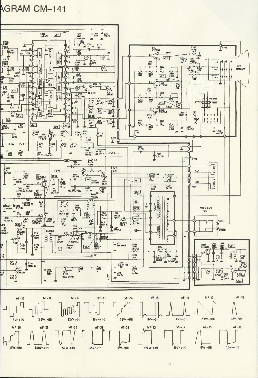
SCHEMATIC DIAGRAM ............................................................................................................ 23
PRINTED CIRCUIT BOARD ...................................................................................................... 24
~commodore COLOR VIDEO MONITOR
JULY 1984
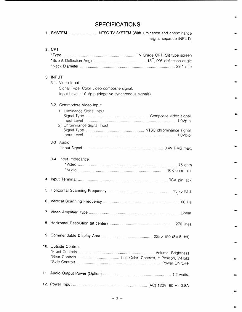
SPECIFICATIONS
1. SYSTEM ......................... NTSC TV SYSTEM (With luminance and chrominance
signal separate INPU I).
2. CPT
-Type ............. ....... TV Grade CRT, Slit type screen
• Size & Deflection Angle ............................................... 13", 90° deflection angle
- Neck Diameter ....................................................................................... 29.1 mm
3. INPUT
3-1. Video Input
Signal Type: Color video composite signal.
Input Level: 1.0 Vp-p (Negative synchronous signals)
3-2 Commodore Video Input
1) Luminance Signal Input Signal Type ....................................... Composite video signal Input Level. ............ ...... ........... . ................................. 1.0Vp-p
2) Chromlnance Signal Input Signal Type .................................... NTSC chrominance signal Input Level... .... . ... ... ... ....... .. ... ........................ 1.0Vp-p
3-3 Audio
-Input Signal .. ............................................ OAV RMS max.
3·4 Input Impedance -Video
- Audio
4. Input Terminal.
5. Horizontal Scanning Frequency.
..... ....... 75 ohm
... 10K ohm min.
RCA pin jack
. ........................... 1575 KHz
6. Vertical Scanning Frequency. . ...... .................................................. 60 Hz
7. Video Amplifier Type
8. Horizontal Resolution (at center)
9. Commendable Display Area
10. Outside Controls • Front Controls • Rear Controls
-Side Controls ......................... .
11. Audio Output Power (Option) .
12. Power Input
... ... ....... linear
.................. ............................... 270 lines
. 235 x 190 (S x S dot)
............................. Volume, Brightness ........ Tint. Color, Contrast. H-Posltlon, V-Hold
..... . ........ Power ON/OFF
' .. 1.2 watts.
........................ (AC) 120V, 60 Hz O.SA
- 2 -
..
--
-....
--

--------------.... - _______________ , _______ • ___ ,_.w,. ......... ________________ _
IMPORTANT SERVICE SAFETY PRECAUTION
Service work should be performed only after you are IhorooghIy t.niliar wittl aI 0( the loIIowing safety checks and S8fviclf1g gUIdelines
WARNING
1. No modification of any circuit should be attempted for continued safety,
2. Disconnect tne AC plug from the AC outlet before repillcing parIS. .1 Semiconductor heat sinks should be regarded as potential stlock
hazards when the chaSSIS is operating. 4 The chassis in this receiver is hot (connected to one side 0( the
AC ~ne). Use an isolatIOn transformer between the line cord and power recep~, when servicing ttlis chassis.
;;ERVICING Of' HIGH VOl T AGE SYSTEM AND PICTURE TUBE
When servicing the high voltage system, remove the static charge by connecting a 10K ohm Resistor in series with an Insulated wire (such as a test probe) between ttle chassis and the anode lead. (AC
!llle cOfd should be disconnected from AC outlet,)
1. Picture tube in this receiver employs integral Implosion protectIOn. 2. Replace with tube of the same type number for continued safety. 3 Do not lift picture tube by the neck. 4 Handle the piclure tube only when weanng shatter-proof goggles
and after discharging the high voltage completely.
X RADIATION AND HIGH VOLTAGE LIMITS
1. Be sure your service personnel are aware of the procedures and instructions covenng X-radiation The only potential sources of Xray In current sold state TV receivers is the picture tube. However, the picture tube does not emit measurable X-ray radiations if the high voltage is kept at factory·set levels It is only when hlQh voltage IS excessive that X -radiatIOn is capable of penetraling the shell of the picture tube including the lead In glass matenal. The important precautIOn IS to keep the hlQh voltage at factory-set leVels,
q It is essential that servicemen have available at all times an accurate high voltage meter. The calibration of this meter should
be checked periodically. 3. High voltage should always be kept at rated value no higher.
Operalion at higher voltages may cause a failure of the picture tube or high vo~age Circuitry and, also, under certain conditIOnS, may produce radiatIOn In excess of desirable levels When the high voltage regulator is operating properly there is no possibility of an X-radiation problem. Every time a color chassis IS serviced, the brightness should be tested while monitonng the high voltage with a meter to be certain that the high voltage does not exceed the specified value and that it is regulating correctly.
-3-
X-RADIATION AHa HIGH VOlTAGE LIMITS (Continued)
5. Do not use a picture tube other than that spedl8d Of make unrecommended circuit modificattonS in the high voltage circuitry.
6. When trouble ~ and taking lest measurements on a receiver With an excessive high voltage, avoid being unnecessarily close to the receiver. Do not operate the receiver longer thcw1 is necessary to locate the cause of excessive voltage.
BEFORE RETURNING THE RECEIVER (Fife & Shoctc Hullrd)
BefOfe returnlf1g the receiver to the user, perform the follooMng
safety checks.
1. Inspect aN lead dress to make certain that leads are not pinched Of that hardware IS nd lodged between the chassis and other rne1a1 parts in the rec~ver.
2. Inspect all protective devices such as non-metallic control knobs. IllSUlating fish papers, cabinet backs, adjustment and compartment covers or shields, isolation resistor-capacity netwOfks. mechanical insulators etc.
3. To be sure that no shock hazard exists, check for leakage current in the following manner, • Plug the AC line cord directly into a 120 volt AC outlet.
(Do not use an isolatIOn transformer for thiS test) • Using two clip leads, connect a 1,5K ohm. 10 watt resistor
paralleled by a 0 .15uF capacitor in series with an exposed metal cab4net parts and a known earth ground, such as water pipe or conduit
• Use a VTVM or YOM with 1000 ohm per volt, or higher. sensitivity to measure the AC voltage drop across the resistor (See Diagram).
• Move tne resistor connection to earth exposed metal part having a return path to the chassis (antenna. metal cabinet, screw heads. knobs and control shafts, escutcheon, etc.) and measure the AC voltage drop across the resistOf. All checks must be repeated with the AC line cord plug connection reversed. (If necessary, a non-polarized adapter plug must be used only for the purpose of comple\lng these checks.) Any reading of 0.3 volt RMS (this corresponds to 0.2 milliamp. AC.) or more is exces5lve and Indicates a potential stlock hazard Which must be corrected before returning the receiver to the owner.

---------------------------------------.--------------------------------------
IMPORTANT SERVICE SAFETY PRECAUTION (Continued)
TO EXPOSED METAL PARTS
CONNECT TO KNOWN EARTH GROUND
- 4 -
SAFETY NOTICE Many electrical and mechanical parts in television receivers have special safety-related characteristics. These charactenstics are often not evident from visual Inspection nor can the protectIOn afforded by them be necessarily increased by using replacement components rated for higher voltage, wattage, etc. Replacement parts which have these special safety charactenstlcs are Identified In this manual; electncal components having such features are identified by "@"and shaded areas In the Replacement Parts Lists and Schematic Diagrams. For continued protection, replacement parts must be identical to those used In the original CirculI. The use of a substitute replacement part which does not have the same safety characteristics as the factory recommended replacement parts shown In this service manual, may creilte shock, fire, X radiation or other hazards.
.. til>
...
...
-..
...
MAJOR CIRCUIT FEATURES
1. Newly developed components. Hybrid-IC type STR 470A serves the stable B + output against input and load variations. In application of this reliable component, the power Circuit has merits as listed: a No adjustment for B + (DC115) output IS necessary. b. Simplification of the circuit. c. No voltage setting against the variation of main power voltage
is necessary. 2. MSI (Medium Scale Intergrated Circuit)
This Monitor Consists of 3 MSls. Each MSI IS prOVided with the function of the conventional circuits, which enables rt to improve reliability and stability of picture quality by reducing the number of parts and adjusting points.
3. Low Loss Vertical Output CircuIt. The power loss In the vertical output circuit IS reduced by changing over from high voltage to low voltage In the front and back halves of the scanning period.
4. High voltage Circuit FBT (flyback transformer) is multl-smgle type, that is, high voltage rectifier diodes are connected, between high voltage windmg, and these are sealed. This FBT decreases the variation of picture size and reduces the dragging of the picture. The raised high voltage improves focussIng to make picture quality better.
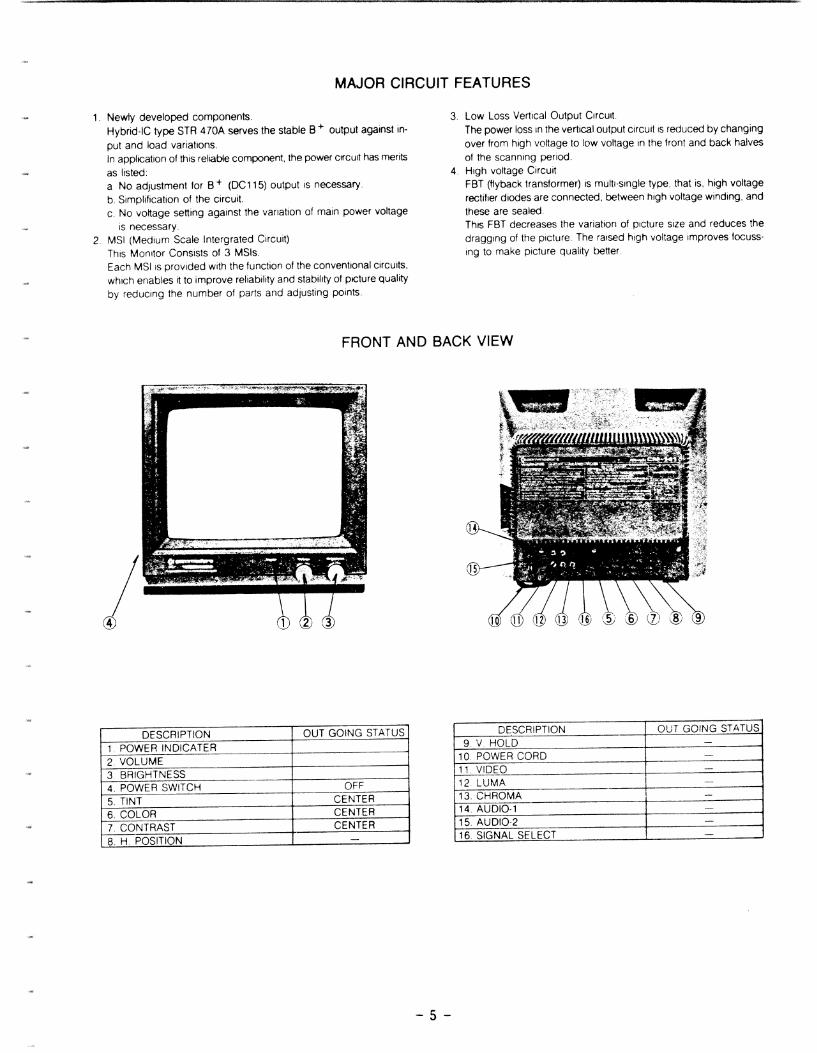
FRONT AND BACK VIEW
DESCRIPTION OUT GOING STATUS DESCRIPTION OUT GOING STATUS 1. POWER INDICATER 9. V HOLD -2. VOLUME 10. POWER CORD -3 BRIGHTNESS 11. VIDEO
4. POWER SWITCH OFF 12. LUMA -5. TINT CENTER 13. CHROMA -6. COLOR CENTER 14. AUDIO-1 -7. CONTRAST CENTER 15. AUDIO-2 -
8. H. POSITION - 16. SIGNAL SELECT -
-5-

, ............ ------------------.... --------------------....... ----.... --_ ... _ ........ ----...... ----~--............ --
CIRCUIT DESCRIPTIONS 1, POWER SUPPLY
This Monitor power supply IS switching mode power supply (SMPS) that is consist of sWitching IC (IC901), SMPS TRANSFORMER (TOO 1 )
pulse TRANSFORMER (T902) and assoCiated component The BasIC theory of the SMPS IS the circuit of Blocking Oscillation and by tur' ning ON, OFF of STRA470A. the secondary of the SMPS TRANS is applied the pulse, Instant + 115V DC that pulse is rectlflred IS abtalns.
All other operating voltage and pulse are drlved from the secondary winding of the high voltage transformer (also
called FBT. T703)
2. ST Mn UP CIRCUIT
An Initial start·up Circuit provides drive to the horlzontlal output stage
when the set IS Initially turned on ThiS CIrcUIt consists of 0703 and associated components It proveds the Initial voltage necessary to activate IC701 and pro· vldes a drive pulse to the hOrizontal drive transistor 0701
Once the FBT·drived voltages operational 0708 IS forward· biased and 0701 is reverse-biared. prOViding + 45V DC to IC701 and 0701
SWitching voltage supply CirCUit like tr,IS results In saving power consumption
3. HORIZONTAL DEFLECTION SYNCHRONIZATION AND
VERTICAL
Integrated Circuit IC701 perlorms the hOflzontal synchronIZation (also called horizontal oscl'lator) A hOrizontal rate output pulse IS coupled from IC701 pin 15 to
hOrlzontai driver 0701. The driver stage dflves the hOflzorltai out put 0702. HOrizontal synchronization slg'1al IS derived fronc composite v'deo Signal which coupled to IC701 pin 10.
Vertical synchronization signal '5 derived from composite signal at IC701 pin 8 and coupled to pin 7 through R601
4. HORIZONTAL AFC AND OSCILLATION LlMITIER
AFC Circuit IS conSists ot phase detection CirCUit of IC701 and 0704. associated component Oscillation limiT CirCUit .s necessarv to P'8-vent from excessive high voltage. ThiS CirCUit IS located In IC70 1
and controls the OSCillator to maintain the control signal In correct frequency and phase w'th the hOfllonta' sync signal
5. X-RAY PROTECTION CIRCUIT
Hle X-ray protection CIiCUltlS consists of 0703. R731 (Hold. Down)
R729. R730 and assoCiated ccmponent that connected to pl'l 16 of IC701 A pulse j'om ~BT Pl~i 6 is rectified by 0705 Under normal operating condlt!OrlS. tne resui'a'lt voltage maintains at specified value
If a rna!f,mctlon causes excessive nigh vOltage. me amplitude of pulse from FBT Increases. cauSing a corresponding Increase In 0703 which results In vos!tage Increase at pin 16 of IC701. Voltage In
crease at IC701 pin 16 makes Xray protection cirCUit conduct and hOrizontal oscliatlon operation no longer function.
The C!fCUlt wlil latch as above and the IIlstrument IS necessary to turn off for at least 30 seconds to function again
6. VERTICAL OSCILLATION/DRIVE CIRCUIT
Vertical oscillation and drive CirCUit are located In IC701 R603. R605. R606 C604 and R604 which connected at IC701 pin 6 are time constant CirCUit that determine the verllcal OSCillation frequency Vertical size control function IS performed by R604 causing the negative feed back to change.
7. VERTICAL OUTPUT
0601 and 0602 are SRPP (SHUNT REGULATED PUSH PULL) vertical output cllcuit. 45V-supply through 0604. 0605. C6Q8 is the main voltage supp
ly line R620. C613. 0603 IS pump up circurt whICh supplies sufflCl9nt current driVing the first half of vertical scan
8. HORIZONTAL DRIVE CIRCUIT
To obtain horizontal drive Du'ses irOrr! IC70t Din 15 the honzon
tal OsCli!3tor must be wor"ng. Horizontal dnve pulses Irom IC701 pin 15 are applied to hOrizontal driver 0701. 8 + for 0701 \S is supplied from 45V line through 0708. OU'lng ''l'lial receiver turn·on before the FElT -DRIVED
SUPPL Y VOLTAGE ARE DEVELOPED. 0701 IS s,,)plied Initial B + from the regul,'ted 115 volt I:ne through R736
9. HORIZONTAL OUTPUT
Horizontal dnve pulses from 0701 are coupled through T703 CO
the bare of hOrlzon[al output 0702. 0702 is biased on when the
beam IS at about mid-screen. The charge stored on C724. C729 cause~current to flow through the hOrizontal yoke Winding and 0702 to g'JI_!IId. When the beam reaches the fight Side of the screen. 0702 IS turned off and the current In the yoke IS dllected Into C719. C720 At the same time
current flows Into C719. C720 from the regulated B + via the FBT pnmary Winding
Due to resonance. the current then reverses ard flows back through the hOllzontai yoke Winding Into C724, C729 This action aefects the electron beafT1 back to the 4- 115V regulated B + .
10. PINCUSHION CORRECTION
Pincushion correction CIICUlt IS T702 and ItS associated components. HOrizontal yoke current IS Increased or decreased In response to vertlca' parabola pulse The CirCUit of 0751 0752, T751 and
assoclatea component. IS for Improving high voltage translcent response
11. POWER SUPPLY DETAIL DESCRIPTIONS
- 6 -
RCC (RINGING CHOKE CONVERTER)
1. Basic circuit and its operation
+ r:;-r~~ R902 fB.) ; I~ ~92;1' V~O<:qJ~
C913 I. 0
R904 -0 ~
01 ~ -
~-------~--------~
a) 01 IS biased by the starting resistor R902 and 01 becomes ON.
b) Induced voltage will appear at base drive winding "B" And the loop current thru C913. R904. 01BE and "B" IS added on bias current made by starting resistor.
c) Collector current of 01 is increased rnaking linear curves
d) At thiS moment. there IS Induced voltage at secondary Winding but It is blocked by 0909.
e) Collector current is Increased but rt is limited because base cur
rent IS cons:ant. The limited current, threshold pOint IS Hie x lb. 01 is n until collector current reaches this point.
-
..
--
-
-
...

f) During Q1 is ON, input vonage Yin is added on the primary winding P But, it is added on Q1 C-E suddenly.
g) At same time, inverted voltage appears at "B" which will bias Q1 B·E reversely and Q1 is OFF.
h) The energy charged in P is discharged by the secondary winding S thru D909.
i) Q1 B-E biased reversely. j) The energy is discharged thru D909 and when Id is zero,
starting current by R902 makes Q1 on again. Repeating from (a).
2. Operation circuit (1) The operation Circuit has function for voltage regulation
in addition to the basic cirCUIt. When the output voltage is going to increase. base drive cur·
+
Yin
here:
(In the actual case, restart is made by leakage inductance of the transformer and after starting by R902, switching of Q1 is kept continuously without R902.)
* Energy charged in P is 1/2 X Ll2 * The curves of collector current at Increasing is soft if induc·
tance is large. The larger, the softer. Natural fold back characteristics is given to this circuit against over load and output short, so, addibonal protection circuit is not needed.
rent is going to decrease, so that Ql IS switched off during small collector current and the output voltage is regulated.
.---Dl-__ ~ +
0909
S C920 Vout •
________________________ J
If the output voltage is going to exceed rated voltage. Q3 IS switched on and Q2 is switched on and base current for Ql IS proportionately decreased Voltage regulation IS done like this.
Yin Switching frequency F IS X k lout x L
proportionate to input voltage and reversely proportionate to output current and inductance.
+
3 fo.-. __ --.
(2) If the output voltage is directly detected. the regulation ac· curacy is Improved. But the secondary will not be insulated from primary. (Hot chassis) In order to make cold chassis. voltage detecting winding is to be added. The output voltage IS regulated indirectly and secondary w,1I be insulated from primary. When this detecting winding is added. the Winding construc· tlon is to be conSidered to get coupling characteristics. Split each winding Into two and construct sandwich windings to im· prove load regulation.
0909 .--1::.1--_---0 +
C920 Vout s •
I
~---~T-----------~2: L ___________ - - -- - - - - - -_ ...
- 7 -

(3) It IS possible to use the former SMPS at free running frequency as mentioned above. But it IS also possible to lock the switching frequency to hOrizontal frequency In the latter case, frequency is constant and only Ton IS changed. This IS pulse Width MOdulation (PWM) tf this IS applied to CTV, the time of sWitch on IS met to blanking time of CRT and nOise suppression IS easier than free frequency If locking to some frequency IS needed, the primary Induc-
(5) Operation circuit for frequency iock;ng
0907
R902 C914
?C913 V,n
I I R904 I I
I I t _ ______
P
tance shall be determined so that the free running frequency before locking may be smaller than the honzontal frequency even if at worst case. 0Norst case means that Vin IS maximum and 10 IS minimum. The Fo will be the highest dunng free running without locking.)
(4) The wave shape of voltage and current at free Fa and lockIng respectively.
I I I
0909
I(s c:+ ::"
R909 0908
~~--------_~_~_-_-_-_--__ --_£_-_-_-_-_-_~ __ J
- 8 -
..
~\
-...
-
t.D
(OMPOSITE VIDEO
COMMODORE VIDEO
AUOIO-2 INPUT
AUOIO-1 INPUT
~ ( VIDEO INPUT LUMA
[~ m
)
INPUT
TERMINAL
BOARD
AC LINE
60Hz
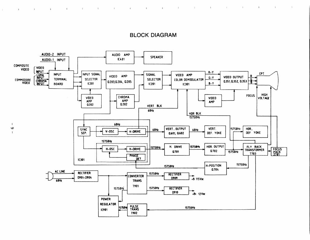
BLOCK DIAGRAM
AUDIO AMP I--1(401
SPEAKER
SIGNAL VIDEO AMP R-Y (PT /I VIDEO AMP
SELECTOR SElEClOR (OLOR DEMODULATOR G-Y VIDEO OUTPUT
1(201 0.203,0.204, 0.205 0.351,0.352,0.353 1(201 1001 8-Y
§ INPUT "GNAl
I N L.l
VI'oEO FOCUS HIGH
VOL TKf. AMP 0.202
rsYNcl ~
VERT BlK
60Hz
r _____________ J~Hz I -----------------,------., H V-OSC H V-DRIYE III 60Hz .. I ~-- .. -____ ...................... __ .. _ .. __ ................................ J
15750Hz r-.......................... -........................................ -- ..... -----,
HOR 8lK 1575CHz
VERT. OUTPUT 60Hz VERT. 0.601, 0.602 DEF. YOKE
H. ORIYE 11575.t4z I HOR. OUTPUll 1 ~ FLY BACK 0. 701 .. 0.702 15750Hz TRANSFORMER
1703
: : L-------~:i~~ ,
1(301
RECTIFIER 0901-0904
: t_ .......................... _ .... _ .. __ ........ L_-_-__ -_-_-r:!:..:~J
1---...----.-1-1 eONYERTER
TRANS
15750Hi T901
...-
POWER
REGULATOR ~ I PULSE ~ TRANS le901 T902
15750Hz 15750Hz I H-POSITION 0.704
15750Hz I RECTIFIER .. 0909 +B 115Yoc
15750Hz r RECTIFIER .. 0910
+BI 12Voc
15750Hz

-----------------------------,---------------------------
IC301 VIDEO/CHROMA
DL201
R314 COLOR-SYNC
IH DELAY LlNE-__
T201 BANDPASSTRANv __ ~~~ __
IC201 SWITCHING IC
IC401 SOUND IC
CHASSIS TOP VIEW
R625 V-CENTER
T703 FBT
L704 H. WIDTH COIL
~CREEN
~FOCUS
R731
,R355 R DRIVE
~ R351
B. DRIVE
R362 B. BIAS
R358 R. BIAS R3S4 G. BIAS
HOLD DOWN IC701 IC901 R708 R609 R329 VERT/HORIZ STR470A H.HOLDER V SIZE SUB BRIGHT
-10 -
-

COMPONENT AND TEST POINT LOCATION
P402 P201
[] ~fiJ ~ []
P401 IC401 []
T901
OIL----' P902
P901
R3548) B.BIAS
R3588) R.BIAS
R3628) G.BIAS
P202
B E
~ Q202
IC901
00 P2 PI
P352 e
C.P.T. P.W.B.
o T20 I
R609 IT' VSIZE'-..V
Q601
IC701
Q,p, • TP4
H.HOLD
r-rR~08 \..!..IT P7
DL201
D T P 6 ••
TP5
• TP9
COLOR SYNC
R314
EJQ L704
-o t!l.
IC301
IJ P301
V. CENTER R625
C\I~ (f) I'L\ g V R731 !l. HOLD DOWN
SUB BRIGHT R329
TINT f31 I
e p351
IL::\VIDEO
\bR355 R DRIVE
@R351 BDRIVE
COLOR R305
-11-
TPI •• CONTRAST H. POSITION V. HOLD TP 2 R302 R7 17 R604
MAIN P.W.B.
P302
• r::l TP 8 P703

INSTALLATION AND SERVICE ADJUSTMENTS
1. GENERAL INFORMATIONS
All adjustments are thoroughly checked and corrected when the monitor leaves the factory. Therefore the monitor should operate normally and produce proper colour and pictures upon Inslalla· lion However, serveral minor adjustments may be reqUired depen ding on the particular iocatlon In which the monitor IS operate de ThiS monitor IS shipped completely In cardboard carton. Carefully draw out the monitor from the carton ad remove all packing materrals Plug the power cord Into a convenient 120 volts 60 Hz AC power outlet Never connect to direct current or any other power outlet or frequency Check and adjust all the customer controls such as BRIGHTNESS, CONTRAST, and COLOUR Fin: Controls to obtain natural colour or BNV picture
2. AUTOMATIC DEGAUSSING
A degaussing coil IS mounted around the picture tube so that ex ternal degaUSSing after moving the monitor IS normally un necessary. providing the monitor IS properly degaussed upon in· stallatlon. The degaUSSing coil operates for about 1 second after the power to the monitor is switched ON. If the set IS moved or faced in a different direction, the power SWitch must be switched off at least 10 minutes In order that the automatic degaUSSing Clr CUlt operates properly. Should the chaSSIS or parts of the cabinet become magnetized to cause poor colour punty, use an external degaUSSing coil. Slowly move the degaussing COil around the faceplate of the picture tUbe. the sides and front of the monitor and slowly Withdraw the coil to a distance of about 2 meters before disconnecting It from AC
source. If colour shading still perSists, perform the COLOU8 PURITY ADJUSTMENT and CONVERGENCE ADJUSTMENTS procedures, as mentioned later
3. HIGH VOLTAGE CHECK
CAUTION: There IS no HIGH VOLTAGE ADJUSTMENT on this chaSSIS The + 115 volt power supply must be pro
perly adjsuted to Insure the correct high voltage.
1. Connect an accurate high vohage meter to the second anode of the picture tube
2 Turn on the move. Set the BRIGHTNESS and CONTRAST CO'l' trois to minimum (zero beam current)
3. High voltage will be measured below 25KV. 4 Rotate the BRIGHTNESS Control to both extremes to be sure
the high voltage does not exceed the limit of 25 KV under any conditions.
4. FS CIRCUIT CHECK (Hold down)
The Fail Safe (FS) Circuit check IS Indispensable for the final check in the servIcing checking should De done following the steps below 1 Turn t~e power srw ON and adjust customer controls for nor. mal operation
2 Connect a VTVM between TP7 (the cathode of 0703) and the chaSSIS ground
3 Adjust Bllghtness, contrast color volume for mechanical minimum
4 Adjust Hold down VR (R731) on the main Board for the voltage at TP7 (the cathode voltage of 0703) IS 10 3 ± 002V DC
5 After the adjustment ot the voltage. fiX the Hold down VR (R731) With silicon bond
6 Check the set IS In hold down mode when the voltage of TP7 (the cathode voltage of 0703) is 13.2V + 05, - OV
7 if this monitor is not the Fail Safe (FS) repeat steps 1 through 5
5. HORIZONTAL OSCILLATOR ADJUSTMENT
If there is an Indication of unstable horizontal sync adjust the HORIZONTAL HOLD COntrol (R70a). Adjust the HORIZONTAL HOLD Control to the centre of the pull-in range
6. VERTICAL OSCILLATOR ADJUSTMENT
If the picture moves up or down on the screen. adjust the VERTICAL HOLD Control (R604) at the back of the monitor until there is a Single Image without vertical movement
7. VERTICAL SIZE ADJUSTMENT
VerticalSize Control (R609) on MAIN Board changes the size of the picture or pattern, haVing an equal effect on the top and bot tom. Make final adlustmen, for V-size of picture is 190 mm.
8. FOCUS ADJUSTMENT
Adjust FOCUS Control on FOCUS PACK n01 for well defined scanning lines In the 1/4 and 3/4 pOint of the screen.
9. HORIZONTAL WIDTH ADJUSTMENT
Adjust the Horizontal Width control coil (L 704) by turning it With a hexagonal adJusling tool so that the Width of the picture (OAT A DISPL Y AREA) IS 240 mm
10· COLOUR SYNC. ADJUSTMENT
1. Tune In a colour program and warm up for five minutes 2 Connect terminal TP5 (the pin a of the IC301) and TP6 With
a short Jumper wire 3 Then the colour stripes Will appear on the screen when the
adjustment IS Incorrect. Adjust the colour sync. VR (R314) so that the colour bar pattern stand still
4 Remove the short jumper wire.
11. COLOUR PURITY ADJUSTMENT
-12 -
NOTE: Before attempting any pUrity adjustments. the monitor should be operated for at least fifteen minutes
1 Receive a video signal (raster) to the Video Input terminal 2 Demagnetize the picture tube and cabnet uSing a degaUSSing
coil 3 Turn the CONTRAST and BRIGHTNESS Controls to maximum 4 Adjust RED and BLUE CUT OFF controls (R358 and R354) to
prOVide only a green raster. Advance the GREEN CUT OFF Control (R362) if necessary
5. Loosen the clamp screw holding the yoke and slide the yoke backward or forward to provide vertical green belt (lone) in the picture screen.
6. Remove the rubber Wedges. 7 Rotate and spread the tabs of the pUrity magnet (See figure
13) around the neck of the picture tube until a green belt is ob· tained in the center of the screen. And at the same time, center the raster vertically by adjusting the magnet.
8 Move the yoke slowly forward or backward until a unrtorm, green screen is obtained. Tighten the clamp screw.
9 Check the purity of the red and blue raster by adjusting the CUT OFF Controls.
10 tighten the clamp screw of the yoke temporarily. 11. Obtain a white raster; refernng to "CRT GRAY. SCALE
ADJUSTMENT' 12. Proceed With convergence adjustment.
..
...
..
-
12. SUB·BRIGHTNESS ADJUSTMENT
1. Supply whrte color with a computer to the video input terminal. 2. Turn the contrast to be MAXIMUM with the contrast volume
(fully clockwise) and BRIGHTNESS to be MINIMUM with the Bright Volume (fully count clock wise).
3. Adjust the Sub-Bright Volume (R239) to cun off the picture slightly.
13. VERTICAL CENTER ADJUSTMENT Adjust the V-Center Contra! (R625), so that the center of picture is the same as the mechanical center of color picture tube.
14. BAND PASS TRANS ADJUSTMENT (T201)
1. Supply a video signal to the Video input terminal 2. Connect oscilloscope probe to the base of Q202. 3. Turn the core of T201 so that the 3.58 MHz signal IS
maximized.
15. 3.58 MHz TRAP (DL201)
1. Supply a video signal to the video input terminal 2. connect oscilloscope probe to the pin 27 of IC301. 3. Turn the core of PL201 so that the 3.58 MHz signal is
minimized.
16. WHITE BALANCE ADJUSTMENT
-13-
1. Remove the input signal. 2. Remove the connector of the P351. 3. Short the terminal TPI and TP2 with a jumber wire. 4. Turn the screen control fully counterclockwise. 5. By rotating the RED, GREEN, and BLUE bias controls (R358,
R354, R362) counter clockwise from the maximum. set them to the 1/3 position.
6. Set the RED and BLUE DRIVE CONTROLS (R355, R351) to the mid-position.
7. Turn on the Monitor. 8. Rotate the SCREEN CONTROL gradually clockwise until the
first horizontal line appears
9. Set the line to be white color with the other two Bias Con· trois (Except the first color Bias Control).
10. By Rotating the screen volume counter clockwise. adjust for the point that the horizontal line appears faintly.
11. Remove a jumper wire between terminals TPI and TP2. 12. Adjust the RED and BLUE DRIVE CONTROLS to obtain pro·
per white balanced picture in high light areas. 13. Rotate the BRIGHTNESS and CONTRAST CONTROLS to ob·
tain dark gray raster. Then check the white balance in low brightness. If the white balance is not proper, retouch the BIAS CONTROLS and DRIVE CONTROLS to obtain a good white balance in both low and high light area.

17. CONVERGENCE ADJUSTMENTS
NOTE: Before attempting any convergence adjustments, the receiver should be operated for at least fifteen minutes.
Contre Convergence Adjustment
1. Supply crosshatch pattern with a color bar signal generator to the video Input.
2. Adjust the BRIGHTNESS and CONTRAST Controls for well defined pattern
3. Adjust two tabs of the 4-Pole Magnets to change the angle between them (See figure 2) and superimpose red and blue vertical lines in the center area of the picture screen. (See figure 2)
4. Turn the both tabs at the same time keeping the angel constant to superimpose red and blue hOrizontal lines at the centre of the screen. (See figure 3)
5. Adjust two tabs of 6-Pole Magnets to superimpose red/blue line and green one. adjusting the angle affects the vertical lines and rotating both magnets affects the hOrizontal lines.
6. Repeat adjustments 3.4,5 with understanding red, green and blue movement. because 4-Pole Magnets and 6-Pole Magnets have mutual affection and it makes dots movement complex
RUBBER WEDGES
ADHESIVE TAPE
DEFLECTION YOKE
GLASS CLOTH TAPE
CONVERGENCE MAGNET ASS'Y
/
31 mm (1-3/16")
FIGURE 1.
• Circumference Convergence Adjustment 1. Loosen the clamping screw of deflection yoke to allow the yoke
to tilt 2. Put a wedge as shown in figure 1 temporarily. (Do not remove
cover paper on adhesive part of the wedge.) 3. Tilt front of the deflection yoke up or down to obtain better
convergence In circumference. (See figure 1 push the mounted wedge into the space between picture tube and the yoke to fiX the yoke temporarily.
4. Put other wedge into bottom space and remove the cover paper to stick.
5. Tilt front of the yoke right or left to obtain better convergence in circumference. (See figure 1)
6. Keep the yoke position and put another wedge in elghter up-per space. Remove cover paper and stick the wedge on PiC-ture tube to fix the yoke.
7. Detach the temporarily mounted wedge and put it in another upper space. Stick it on picture tube to fix the yoke
8. Atter fixing three wedges, recheck overall convergenc. Tighten the screw firmly to fix the yoke and check the yoke is firm.
9. Stick 3 adhesive tapes on wedges as shown in figure 1.
TEMPORARY MOUNTING
1 RUBBER WEDGE
\
<Yt ADHESIVE
RUBBER WEDGES LOCATION
RUBBER WEDGES KIT
ADJUST THE ANGLE r-----:;;;>""4-POLE MAGNETS (VERTICAL LINES)
PURITY MAGNETS
6-POLE MAGNETS
CONVERGENCE MAGNET ASSEMBLY
FIGURE 2_
-14 -
ROTATE TWO TABS AT THE SAME TIME (HORIZONTAL LINES)
ADJUSTMENT OF MAGNETS
.,
..,
....
---
..
----

BLU RED ,
BLU - _on ~tnl RED -- -- ,
I .-I _
4-POLE MAGNETS MOVEMENT
RED/BLU GRN
REO/BLU-- --nt t I GRN - ---- t
I -l
6-POLE MAGNETS MOVEMENT
Centre Convergence by Convergence Magnets
----8 G R
\ I 1
R 1__ \ 1 _18 G - - G 81--- 1\ --I R
1 \ ~ +-
~- -t---RGB
I~ 'I'. I , I I
, , -711 , I , I
8GR ---I--R ----G
'---- R G 8 - - - - B
INCLINE THE YOKE UP (OR DOWN) INCLINE THE YOKE RIGHT (OR LEFT)
Circumference by DEF Yoke
FIGURE 3. DOT MOVEMENT PATIERN
-15 -
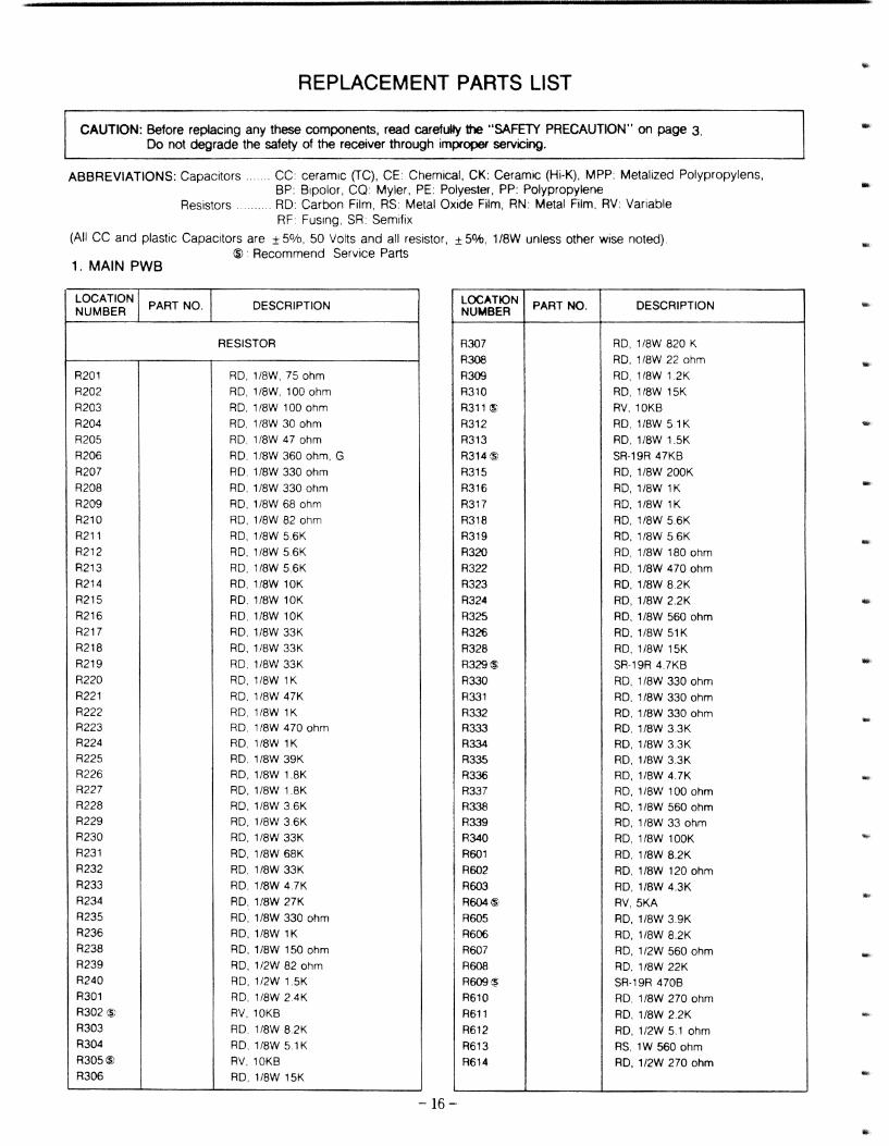
REPLACEMENT PARTS LIST
CAUTION: Before replacing any these components, read carefully the "SAFETY PRECAUTION" on page 3. Do not degrade the safety of the receiver through improper servicing.
ABBREVIATIONS: Capacitors ....... CC ceramic (TC), CE Chemical, CK: Ceramic (Hi·K), MPP Metallzed Polypropylens, BP Blpolor, CO: Myler, PE: Polyester, PP: Polypropylene
Resistors ......... RD: Carbon Film, RS: Metal Oxide Film, RN Metal Film. RV: Variable RF. Fusing, SR: Semifix
(All CC and plastic Capacitors are ± 5%, 50 Volts and all resistor, ± 50ib, 1/8W unless other wise noted). @ : Recommend Service Parts
1. MAIN PWB
LOCATION PART NO. DESCRIPTION NUMBER
LOCATION PART NO. DESCRIPTION NUMBER
RESISTOR R307 RD, 1/8W B20 K R308 RD, 1/8W 22 ohm
R201 RD. 1/BW. 75 ohm R309 RD, 1/BW 12K R202 RD. 1/BW. 100 ohm R310 RD. 1/8W 15K R203 RD. 1!BW 100 ohm R311 ~. RV. 10KB R204 RD. 1/BW 30 ohm R312 RD. 1/8W 5.1 K R205 RD. 1/BW 47 ohm R313 RD. 1/BW 15K R206 RD. 1/BW 360 ohm, G R314@ SR·19R 47KB R207 RD. 1/BW 330 ohm R315 RD, 1/BW 200K R20B RD. 1/BW 330 ohm R316 RD, 1/8W 1 K R209 RD. 1/BW 68 ohm R317 RD, 1/8W 1K R210 RD. 1/8W B2 ohm R318 RD, 1/BW 5.6K R211 RD. 1/8W 5.6K R319 RD, 1/8W 56K R212 RD. 1/BW 5.6K R320 RD, 1/BW 180 ohm R213 RD. 1/BW 5.6K R322 RD, 1/BW 470 ohm R214 RD. 1/BW 10K R323 RD, 1/8W B2K R215 RD. 1/BW 10K R324 RD. 1/BW 22K R216 RD. 1/BW 10K R325 RD, 1/BW 560 ohm R217 RD. 1/BW 33K R326 RD, 1/BW 51K R21B RD, 1/BW 33K R32B RD, 1/BW 15K R219 RD. 1/BW 33K R329@ SR·19R 47KB R220 RD. 1/BW 1K R330 RD, 1/8W 330 ohm R221 RD. 1/BW 47K R331 RD, 1/8W 330 ohm R222 RD. 1/BW 1K R332 RD, 1/BW 330 ohm R223 RD. 1/BW 470 ohm R333 RD. 1/BW 3.3K R224 RD. 1/BW 1K R334 RD. 1/8W 3.3K R225 RD. 1/8W 39K R335 RD. 1/BW 3.3K R226 RD. 1/BW 1.8K R336 RD. 1/BW 4.7K R227 RD. 1/BW 1.BK R337 RD. 1/BW 100 ohm R22B RD. 1/BW 3.6K R338 RD. 1/BW 560 ohm R229 RD, 1/BW 3.6K R339 RD. 1/BW 33 ohm R230 RD.1/BW33K R340 RD, 1/BW 100K R231 RD, 1/BW 68K R601 RD, 1/BW B.2K R232 RD. 1/8W 33K R602 RD. 1/BW 120 ohm R233 RD. 1/8W 4.7K R603 RD. 1/BW 4.3K R234 RD. 1/8W 27K R604® RV. 5KA R235 RD. 1/8W 330 ohm R605 RD. 1/BW 3.9K R236 RD, 1/8W 1K R606 RD. 1/BW B.2K R238 RD. 1/8W 150 ohm R607 RD. 1/2W 560 ohm R239 RD, 1/2W B2 ohm R608 RD. 1/BW 22K R240 RD. 1/2W 1.5K R609~' SR-19R 470B R301 RD. 1/8W 24K R610 RD. 1/BW 270 ohm R302@ RV. 10KB R611 RD. 1/8W 2.2K R303 RD. 1/8W B2K R612 RD, 1/2W 5.1 ohm R304 RD. 1/8W 5.1K R613 RS, 1 W 560 ohm R305® RV. 10KB R614 RD. 1/2W 270 ohm R306 RD. 1/8W 15K
-16 -
...

PRODUCT SAFETY NOTE: Components shaded have special characteristics important to safety. Before replaCing any of these components. read carefully the PRODUCT SAFETY NOTICE of this service manual. Dont degarde the safety of the receiver through improper serVicing.
LOCATION PART NO. DESCRIPTION NUMBER LOCATION
PART NO. DESCRIPTION NUMBER
R615 RD. 1/8W 82K R405 RD. 1I8W 120K R6l6 RD. 118W 12K R406 RD. 1J2W 56 ohm R617 RD. 1/BW 470 ohm R411 RD. 1i8W 12K R618 RS lW 10 ohm ROO1@ RWR, lOW 3.3 ohm R619@ RF. 112W 10 ohm ROO2 RD. l12W l50K R620 RN. lW 4.7 ohm ROO3@ AS. 5W 10K R621 RS. 1W 51 ohm R904 RS. lW 220 ohm R622@ RF. lW 51 ohm R906@ RC, 1/2W 22M R623 RD. 1/2W lK R907® RG. 112W 22M R624 RD. 1/2W 2.2K R90e RN, 1/2W 0.47 ohm R625 (§'. SR19R 47KB R909 RS. lW 56 ohm R627 RD 1:2W 5.1 ohm TH901 THERMITOR PTH 63H)4 SF7 R628 RD. 1/8W 56 K ROM140 R631 RD. 118'/; 1 K
R632 RD. 1!8W 10K I CAPACITOR R630 RS. lW 15K ohm
R701 RD 118W 120 ohm C201 CEo 10uF 16V R702 RD 1/8W 56K C202 CEo 10uF 16V R703 RD 118W lK C203 CE. 10uF 16V R704 RD. 1!8W 68K C204 CK. 103pF + 80"/0. - 20°0 R705 RD 1/8W 15K C205 CK. 103pF + BOG;o - 20D/c
R706 RD. 118W 10K C206 CE. 10uF 16V R70? RD. 118W 10K C207 CC. 39pF ± 50/0
R708 (~J SR19R 10KS C208 CE. 10uF 16V R709 RD. 1!8W 47 ohm C210 CK. 103pF + 80°'0. - 20G/o R710 RD. 1l 8W 470 ohm C211 CK 103pF + 800'0 - 20°'0 R7l1 RD. 1/8W 47K C212 CK. 103pF +80%. - 20e c R7l2 RD. 1!8W 82 ohm C213® SP. 10uF l6V R7l3 RD l18W 47K C214 CEo 10~F 16V R7l4 RD 1/8W 1K C215 CE 220uF 16V R715 RD. 1!8W 22K C217 CK. 103pF + 80°'0. - 200iC
R716 RD 1!8W 12K C218 CEo 47uF 16V R717 ~; RV. 10KB C301 CK. 103p):: ... 800;e - 200~
R718 RD. 1f8W 82K C302 CK. 103pF + 80°'0 -200 "
r1719 RD. 1/8W 4.?K C303 CE, 1uF 50V R720 I RS. 1W 4 7K
R721
I RN l12W 0.47 ohm
R723 RD. 1/2W 150K
R724 RD. 1/2W 1 K
C304 CEo luF 50V
C305 CE. 1uF 50V
C306 CC. 39pF ± 50/0
C307 CK. 103pF + 80°0 - 20°: R725 RD. 1!8W 270K C308 CE, 1uF 50V R726 RD. 1!8W 6.8K C309 CC, 22pF ± 5% R727 RD. 1/8W 390 ohm C310 CC 27pF ± 5°'(0 R728 RD. 1/2W 56 ohm C311 CEo 10uF 16V R729 RD. 1'8W 1K C312 CO 333pF :t 10%
R730 RD. 1 '8'/'1 1 K C313 CC 4700F ± 50 t
R731® SR19R 2.2KB I C31~ CK, 470pF ± 5% R732 RS. 1\N 820 ohm
R733 I RD. l'8W 82K
R734 1
RS. 1i2W 1.5K
R735 RD. 1:8W 39K
C315 CE, 1 ul= 50V
C316 CK 103pF + 80G/o. - 200 '0
C317 CEo 220uF 16V
C318 CEo 4.7uF 50V R736 RD 1/2W 220 ohm C319 CK. 103pF .. 800/0 - 20°.:; R737 RS 1W 1 8K C320 CEo 10uF 16V R74l RD. 1/8W 56K C321 CE, 10uF 16\1
R738 RS. 1W 1K C322 CEo OA7uF 50V R401 RD. l 18W 6 BK C323 CC, 270pF ± 5Q·o
R403 RD. 18W 150K C324 CC. 270pF ± 5°'0 R404 RD. l'8W 47K C325 CC. 270pF + 5°0
-17 -

PRODUCT SAFETY NOTE: Components shaded have special characteristics Important to safety. Before replacing any of these components. read carefully the PRODUCT SAFETY NOTICE of this service manual. Dont degarde the safety of the receiver through Improper servicing.
LOCATION NUMBER
C401 C402 C403 C404 C405
C406 C407 C408 C409 C601 C602
C603 C604® C605® C606 C607 C608
I C609~: C610§
C611 C612
C613~
C614 C615 C616 C617 C618 C619 C620 C631 C701 C702 C703 ~. C704@
C705 C706i§' C707 C708 C709 C710 C711 C712 C713 C714
C715 C716 C717i§'
C718
C.719®
C720® C721 ® C722 C723 C724
C727 C728 C729@
PART NO. DESCRIPTION
CEo 2.2uF 50V CEo 4 7uF 50V CEo 220uF 16V CC, 100pF ±5% CE, 47uF 16V
CE, 220uF 16V CEo 1000uF 16V CO. 104pF ± 10% CK. 103pF +80010. -20%
CE 1uF 50V
CO. 223pF ± 10%
CO. 473pF :c 10°'0 PE. 682pF ± 5% TANTAL 1uF 25V CE, 330uF 16V
CO. 153pF ± 10Ofo
CEo 100uF 50V CE,10uF50V
CE, 3.3uF 50V
CEo 33uF 16V CEo 6.8uF 160V PP, 333pF ± 10% 200V
CE, 100uF 50V CEo 330uF 16V CEo 100uF 16V
CO. 103pF ± 10°'0 CE 220uF 160V CE. 1000uF 25V CEo 180pF ± 10% CEo 47uF 16V CEo 1uF 50V
Cc. 270pF ± 5% PE. 153pF ± 10% PE. 682pF ± 10% CEo 1 uF 50V PP, 562pF ± 10% 200V
CC. 270pF ± 5% CK, 103pF +80%. -200/0 CE. 22uF 16V CE, 33uF 16V CK, 103pF + 80%, - 20% CO, 333pF ± 10%
CK. 270pF ± 10% 500V
CK. 820pF ± 10% 500V CC. 82pF ± 5% CK, 560pF ± 10%
PP.223pF ± 10% 200V CE, 33uF 25V
MPP.682pF ±5% 1.2KV PP, 222pF 15%1.6KV CE, 33uF l60V (H R) CO, 103pF ± 10% SP. 1uF 50V PP. 270pF ± 5% 200V
CE, 4.7uF 250V CC. 470pF ± 5%
PP, 333pF ± 10% 200V
LOCATION NUMBER
COO1® C902@
C903 C904 COO5
C906 C907® C909 C910®
C911 ®
C912® C913® C914
C915 C917 C918®
C919® C920@
C921
C922 C930
C931
0201 i§'
0202 (§.
0203'§:
0204@,
0205@
0301 ~.
0601 ® 0602® 0701@
0702® 0703®
0704®
D201 @ D202@;
D203@ D204@ D205@ D206§
D207 '~.
D601 ~ D602@ D603@ D604@
D605@
-18 -
PART NO. DESCRIPTION
MPP, O.luF 120% 125V
MPP. O.luF ±20% AC 125V CK,472pF 110% CK, 472pF 110%
CK, 472pF ± 10%
CK, 472pF ± 10% CEo 560uF 200V CEo lOuF250V PP, 272pF ± 10% 600V
PP. 123pf ±5% 630V CK,47OpF ± lOOk, 2KV
PE, 154pF ± 2o%. 1 OOV CEo lOuf 160V
CK. 102pF ± 10% 1KV CK. 102pF ± 10% 500V
AC125V 472pF ULtCSA AC125V 472pF ULtCSA CEo 220uF 160V CE, 1000uF 25V CK. 332pF ± 10% SOOV AC125V 4700pF ULCSA
CEo 10uF l00V
TRANSISTOR AND DIODE
KTC 1815·0/Y
KTC 1959·0/Y
KTC 18150ry
KTC 1815·0/Y
I KTC 18150/Y
KTC 562TM·O/Y
MJE 9730 MJE 9730 ..... KTC200S-FA·1 2501453
KTC2229-01Y
KTC 1959-01Y
KDS 1555 KDS 1555 KDS 1555 KDS 1555 KDS 1555 KDS 1555
LED RED (SLP·162B) KDS 1555 KDS 1555 RH·1ZV
1N 4002 RH1AV
•
...
...
..
...
--
--
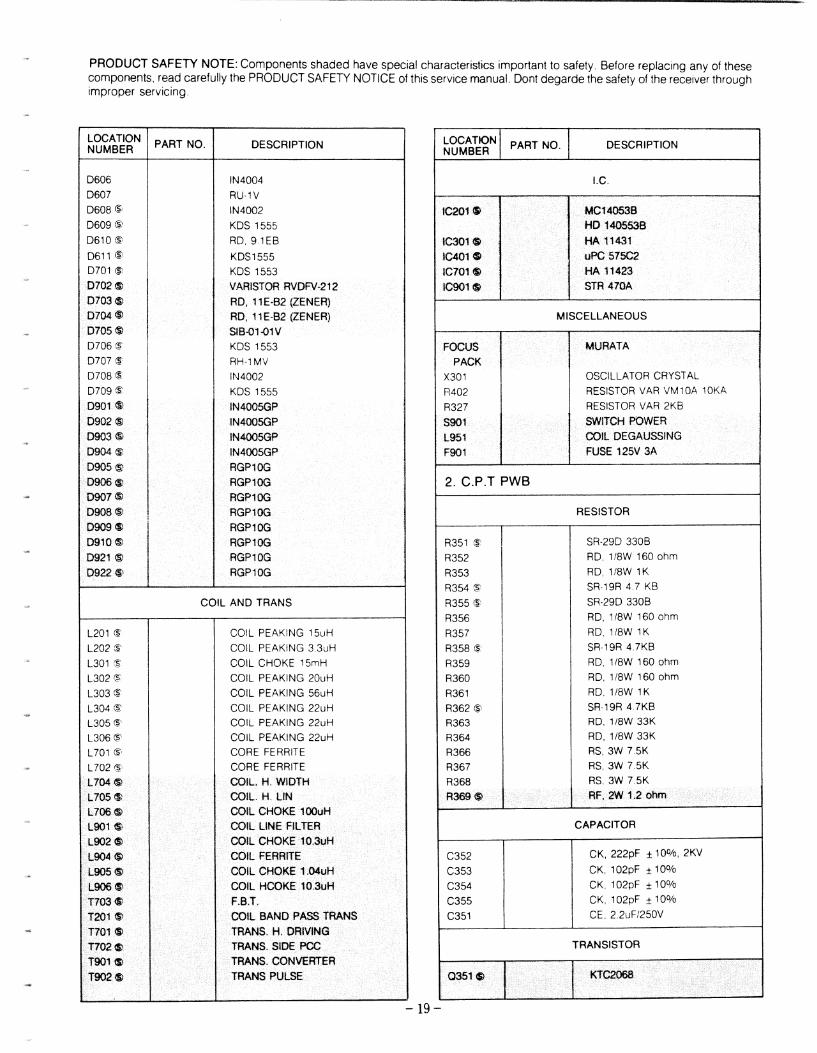
PRODUCT SAFETY NOTE: Components shaded have special characteristics important to safety. Before replacing any of these components, read carefully the PRODUCT SAFETY NOTICE of this service manuaL Dont degarde the safety of the receiver through improper servicing.
LOCATION PART NO. DESCRIPTION NUMBER
LOCATION PART NO. DESCRIPTION NUMBER
0606 IN4004 I.C. 0607 RU-1V 0608 (§. IN4002 IC201 IS MC14053B 0609@ KOS 1555 HD 1405538 0610@ RO,91EB IC301® HA 11431 0611 @ KOS1555 IC401 ~ uPC 575C2 0701 @ KOS 1553 IC701 ~ HA 11423 D702~ VARISTOR RVDFV-212 IC901 IS STR 470A D703® RD, 11E-B2 (ZENER) D704® RD, 11E-B2 (ZENER) MISCELLANEOUS D70S~ SIB-01-01V 0706@ KOS 1553 FOCUS MURATA 0707 @ RH1MV PACK 0708 ~ IN4002 X301 OSCILLA TOR CRYSTAL 0709@ KOS 1555 R402 RESISTOR VAR VM 1 OA 10KA 0901 ® lN400SGP R327 RESISTOR VAR 2KB D902® IN400SGP S901 SWITCH POWER D903® IN400SGP L951 COIL DEGAUSSING D904@ IN4005GP FOOl FUSE 12SV 3A D90S@ RGP10G D906@ RGP10G 2. C.P.T PWB D907® RGP10G D908® , RGP10G RESISTOR 0909~ RGP10G D910® RGP10G R351 @ SR-290 330B 0921 @ RGP10G R352 RO. 1/BW 160 ohm D922@ RGP10G R353 RO. 1/BW 1K
R354 @ SR·19R 4.7 KB COIL AND TRANS R355 @ SR-290 330B
R356 RO, 1/BW 160 ohm L201 @ COIL PEAKING 15uH R357 RO.1/BW1K L202@ COIL PEAKING 3.3uH R35B (§. SR-19R 4.7KB L301 .'§' COIL CHOKE 15mH R359 RO, 1/BW 160 ohm L302@ COIL PEAKING 20uH R360 RO, 1/BW 160 ohm L303@ COIL PEAKING 56uH R361 RO, 1/BW 1K L304@ COIL PEAKING 22uH R362 @ SR-19R 4.7KB L305@ COIL PEAKING 22uH R363 RD, 1/8W 33K L306@' COIL PEAKING 22uH R364 RO, 1/8W 33K L701 @. CORE FERRITE R366 RS, 3W 7.5K L702 @ CORE FERRITE R367 RS, 3W 7.5K
L704® COIL. H. WIDTH R368 RS, 3W 7.SK
L70S® COIL. H. LIN R369® RF, 2W 1.2 ohm L706® COIL CHOKE 100uH
L901 ® COIL LINE FILTER CAPACITOR
L902® COIL CHOKE10.3uH
L904® COIL FERRITE C352 CK, 222pF ± 10%, 2KV
L905~ COIL CHOKE 1.04uH C353 CK, 102pF ± 10%
L906® COIL HCOKE 10.3uH C354 CK. 102pF ± 10%
T703® F.B.T. C355 CK. 102pF ± 10%
T201~ COIL BANDPASS TRANS C351 CE, 2.2uFJ250V
T701 ® TRANS. H. DRIVING
T702® TRANS. SIDE Pee TRANSISTOR
T901 ® TRANS. CONVERTER
T902® TRANS PULSE Q351~ KTC2068
-19 -

PRODUCT SAFETY NOTE: Components shaded have special charactenstlcs Important to safety. Before replaCing any Of these components, read carefully the PRODUCT SAFETY NOTICE of this service manual. Dont degarde the safety of the receiver through Improper servIcing
LOCATION PART NO. DESCRIPTION NUMBER LOCATION PART NO. DESCRIPTION NUMBER
0352@ KTC 2068 0353@ KTC 2068 I
I COIL
L351 ® COil PEAKING 56uH l352 ® COIL PEAKING 56uH l353 ® COil PEAKING 56uH l354 ®, COIL PEAKING 56uH
SPARK GAP
SG351 SPARK GAP SG352 SPARK GAP SG353 SPARK GAP
,
MISCELLANEOUS
SOCKET CPT
3. H.V.C PWB I RESISTOR
R751 RS. 1W 4.7K R752 RN. 1/2W 047 ohm R753 RN. 1/2W 047 ohm
CAPACITOR
C751 CK. 270pF ± 10% 500V C752. CK,820pF ± 10% 500V C753 CC, 82pF ±5% C754(§;
I PP, 274pF/200V ± 50fa C755® I PE, 154pF ± 20%
TRANSISTOR
Q751 ® KTC 2068 FA·1 0752® KTC 2233
TRANS
T751 TRANS. H, DRIVING
4. PICTURE TUBE
C.PT® 370 FCB22-TC04 DY KYS 60037
I - 20-
-
...
-
...
.,
-

TERMINAL VIEW OF SEMICONDUCTOR
DES(RIPTION FIGURE DES(RIPTION FIGURE
KT(1959/KTA562 ~B~ KT(1815 O/Y
KDS1553 KDS1555 --4 Il-RD11E-B2
250 1138( ~ Kl(2233 B ( 1N4002l1N4004 1N4005GP ---1 I
4
STR470A '~3 RGP10G
KT(20681 ~[ 2068-FA-1 B
RU-1AV IRU-1V ---1 If-RH-1ZV IRH-1MV RD9.1EB
~ KT(22290/Y E (
2501453 fC:JfF[
SIB-01-01V
VARISTOR
~ RVDFV-212
-21-

~r~ ~
(3)
f ,
® I
~/
~
,
~/ I ~// @
f f
MECHANICAL DISASSEMBLIES
, ~ I
/~ //1 @
, ,
~4'
• ,
//-" Au ,,/ -
.?'
--'(2)
Q5)
@
;< ;<
•
_.@ @
, /#" ///
NO
I ~~'~_<J. NA"il~_____ _ "!~ ~~_ CABINET Al&'~ ___ ._ L' "~J2J...
11 ,. ,., --i1LQ~ P'-£LAQtf_8.!/( Ui<!s'-L~~~Lf-l2L-+-'---i
~ I ~: ~~i~ 2ffi·g~: ;~~-- : ~~~';-"'::"-,;-?':~'-':~~~'-I-'--1 ,.- .OrOYIA -'PCAfF-coMMmm - ,- -~-T Ji53Yil:1A'- COVfl'l'ASSY~ L,ic~-ABSM_J[):l
0
" I :~:j~:~l!= ~ ~~;=~ ::"~:~~~IXING-~=-.-l=~-=~-~-.------- ~-
8 2' IT T3
" E
" V
" ,,-30 ". Y 3~ ,.-35 J
HF~HFAO
nSl ... " " 12 ~ ~ WASHtA S('~F.W -~fii----
::::::c 1'.;;:.o,;;~=: __ :¥ c=:-:" C-_ -."30~ ~~l~.[A._.'.~NllfQB...:!.~ .. U'. _. __ . '.!" 03270201 rnS2.:])( SA ____ J_
~ ~:~~~fiill=· ~--=-~~= =f-= 4304'4'" MA,lAL r_~T_:~" =- __ ___ --+-i 332\)"",· WASJ.-1ER ." '~,.
03220?0? ~ ~ ~ 4(XH119A
0::m:07(14
~4===---=+--~-----R1S2 • J " PLATE ASSY
.fOO9\!,o, rtAH, ASS)' H''.D S'~j" 3"'·2~rA i-I(lLOfR, PW8 COne) -- EP CHIS,S02038 JJ20lM WASHER, SCRf'W" ------- ---
.070-46.0\ PLATE A,~SY 1ERMI~L-'- lUozY .... 81S .... r 032~~ "§:~_-;'~K!=~~-=: ,- -~- l
332036f\ WA.Sf.'ffl. SCRfw 2 1 i i- ~~J27~~ ~~,O:R.s:~~ff-11 ---~~- ==--==-= +l '19 - "2()W SCR" ..... TAI'PINOS0'fl ---,-----.- ...-
" <:i
" is
O.l;>~'" AfS! -;-;-;-ift·------ ------,--."
.40'~ liND'" CONTROl lUCKY ASIS ..;::r;o,-- -" ~~ ~.--- ---_. __ . __ .... _- ..
13403""" WASHER lN5ULA""f"iON- "2 -~ PS ~-,,----- ------ -;
03401102 RWlA I SCREW, WASHER
l If •
-~-.-- - ---~-. -""'-~.
PRINTED CIRCUIT BOARD
•
2. C.P.T P.W.S
- c;;; -
-24 -

;41
'"',
..
""',


-

n