clk 8 clrld enp qaqb - wakerly home pagewakerly.org/ddpp/student/sxc08.pdf150 digital circuits 8.26...
TRANSCRIPT

145
E X E R C I S E S O L U T I O N S
Sequential Logic Design Practices
874x163
CLR
CLK
LD
QA
QB
2
14
11
1
9
ENP
ENT
7
10
A
B
3
4
C
D
5
6QC
QD15
RCO
13
12
8.1 In the first three printings, change “RAMBANK0” to “RAMBANK1” in the third line of the exercise. The results arethe same. The new expression describes exactly the input combinations in which the 8 high-order bits of ABUS
are 000000012, the same as the original expression using don’t-cares.
8.2 The 16-series devices have or 2048 fuses (see Figure 10–2). The 20-series devices have or2560 fuses.
8.3 There are fuses in the AND array (see Figure 10–4). Each of the eight macrocells has one fuseto control the output polarity and one fuse to select registered vs. combinational configuration in the 16V8R, orto assert the output-enable in the 16V8S. There are also two global fuses to select the overall configuration(16V8C, 16V8R, or 16V8S). The total number of fuses is therefore .
A real 16V8 (depending on the manufacturer) has at least 64 additional fuses to disable individual productterms, 64 user-programmable fuses that do nothing but store a user code, and a security fuse. (Once the securityfuse is programmed, the rest of the fuse pattern can no longer be read.)
8.5 The column below gives the answers in MHz.
Part numbers Suffix
PAL16L8, PAL16Rx, PAL20L8, PAL20Rx -5 5 4 – 4.5 0 117.7 117.7
PAL16L8, PAL16Rx, PAL20L8, PAL20Rx -7 7.5 6.5 – 7 0 74.1 74.1
PAL16L8, PAL16Rx, PAL20L8, PAL20Rx -10 10 8 – 10 0 55.6 55.6
GAL22V10 -25 25 15 13 15 0 33.3 35.7
64 32× 64 40×
64 32× 2048=
2048 16 2+ + 2066=
fmaxE
tPD tCO tCF tSU tH fmaxE fmaxI

146 DIGITAL CIRCUITS
8.6 The column above gives the answers in MHz.
8.7module Eight_Bit_Regtitle ’8-bit Edge-Triggered Register’Z74X374 device ’P16V8R’;
" Input pinsCLK, !OE pin 1, 11; D1, D2, D3, D4, D5, D6, D7, D8 pin 2, 3, 4, 5, 6, 7, 8, 9;
" Output pins Q1, Q2, Q3, Q4, Q5, Q6, Q7, Q8 pin 19, 18, 17, 16, 15, 14, 13, 12;
" Set definitions D = [D1,D2,D3,D4,D5,D6,D7,D8]; Q = [Q1,Q2,Q3,Q4,Q5,Q6,Q7,Q8];
equations
Q := D;
end Eight_Bit_Reg
8.10 If EN or CLK is 0, the output will be stable. If both are 1, the results are unpredictable, since they depend oncircuit timing. It is certain that the circuit’s output will be unstable as long as this condition is true.
8.11 The counter is modified to return to a count of 0 when count 9 is reached.
8.13 The counting direction is controlled by QD: count up when QD=1, count down when QD=0. A load occurswhen the counter is in the terminal state, 1111 when counting up, 0000 when counting down. The MSB is com-plemented during a load and the other bits are unchanged.
Let us assume that the counter is initially in one of the states 0000–0111. Then the counter counts down(QD=0). Upon reaching state 0000, it loads 1000 and subsequently counts up (QD=1). Upon reaching state1111, the counter loads 0111, and subsequently counts down, repeating the cycle.
module Z74x162
title '4-bit Decade Counter'
"Z74X162 device 'P16V8R';
" Input pins
CLK, !OE pin 1, 11;
A, B, C, D pin 2, 3, 4, 5;
!LD, !CLR, ENP, ENT pin 6, 7, 8, 9;
" Output pins
QA, QB, QC, QD pin 19, 18, 17, 16 istype 'reg';
RCO pin 15;
" Set definitions
INPUT = [ D, C, B, A ];
COUNT = [QD, QC, QB, QA ];
equations
COUNT.CLK = CLK;
COUNT := !CLR & ( LD & INPUT
# !LD & (ENT & ENP) & (COUNT < 9) & (COUNT + 1)
# !LD & (ENT & ENP) & (COUNT == 9) & 0
# !LD & !(ENT & ENP) & COUNT);
RCO = (COUNT == 9) & ENT;
end Z74x162
fmaxI

EXERCISE SOLUTIONS 147
If the counter is initially in one of the states 1000–1111, the same cyclic behavior is observed. The countingsequence has a period of 16 and is, in decimal,
8, 9, 10, 11, 12, 13, 14, 15, 7, 6, 5, 4, 3, 2, 1, 0, 8, 9, ...
If only the three LSBs are observed, the sequence is
0, 1, 2, 3, 4, 5, 6, 7, 7, 6, 5, 4, 3, 2, 1, 0, 0, 1, ...
8.14 The only difference between a ’163 and a ’161 is that the CLR_L input of ’161 is asynchronous. Thus, thecounter will go from state 1010 to state 0000 immediately, before the next clock tick, and go from state 0000 tostate 0001 at the clock tick. Observing the state just before each clock tick, it is therefore a modulo-10 counter,with the counting sequence 0, 1, ..., 9, 0, 1, ....
Note that this type of operation is not recommended, because the width of the CLR_L pulse is not well con-trolled. That is, the NAND gate will negate the CLR_L pulse as soon as either one of its inputs goes to 0. If, say,the counter’s QB output clears quickly, and its QD output clears slowly, it is possible for CLR_L to be assertedlong enough to clear QB but not QD, resulting in an unexpected next state of 1000, or possibly metastability ofthe QD output.
8.17 The path from the Q1 counter output (B decoder input) to the Y2_L output has 10 ns more delay than the Q2 andQ0 (C and A) paths. Let us examine the possible Y2_L glitches in Figure 8–43 with this in mind:
3→4 (011→100) Because of the delay in the Q1 path, this transition will actually look like 011→110→100.The Y6_L output will have a 10-ns glitch, but Y2_L will not.
7→0 (111→000) Because of the delay in the Q1 path, this transition will actually look like 111→010→000.The Y2_L output will have a 10-ns glitch, but the others will not.
8.19 The delay calculation is different, depending on the starting state.
In the INIT state, U7 and U8 take 21 ns to propagate the CLEAR signal to the outputs. Then U6 requires 20 nssetup time on its D inputs while U3 requires 20 ns setup time on its RIN input. This implies a minimum clockperiod of 41 ns, assuming zero delay from the control unit.
In states M1–M8, the minimum clock period depends on the delay of the combinational logic in the control unitthat asserts SELSUM when MPY0 is asserted. However, the most obvious way to do this is to connect MPY0directly to SELSUM, creating a delay of 0 ns. This assumption is made below. Also, it is assumed that MPY0 is1 to find the worst case. The figure on the next page shows the worst-case path, in heavy lines, to be 106 ns.Since we would like to use the same clock for all states, the minimum clock period is 106 ns.

148 DIGITAL CIRCUITS
U6 Qoutputs
valid
U2, U3outputsvalid
U4 C4outputvalid
U5 C4outputvalid
U5 Soutputs
valid
U7 & U8outputs
valid
U4 Soutputs
valid
24ns
16ns21ns
16ns
16ns
24ns
27ns39ns
14ns
14ns
24ns
U9 gateoutputvalid
27ns
27ns
U6 Dinputsset up
20ns
20ns
U3 RINinput set
up
20ns
Readyfor nextclock
Clockedge

EXERCISE SOLUTIONS 149
8.20 The synchronizer fails if META has not settled by the beginning of the setup-time window for FF2, which is5 ns before the clock edge. Since the clock period is 40 ns, the available metastability resolution time is 35 ns.The MTBF formula is
Substituting the proper values of and for the ’F74, and of and for the problem, we calculate
8.22 Refer to the sample data sheet on page 169 of the text: “Not more than one output should be shorted at a time;duration of short-circuit should not exceed one second.” In the switch debounce circuit, the short lasts only fora few tens of nanoseconds, so it’s OK.
8.23 CMOS outputs can “latch up” under certain conditions. According to the Motorola High-Speed CMOS LogicData book (1988 edition, pp. 4–10), a 74HCT output can latch up if a voltage outside the range
is forced on the output by an external source. In a switch debounce circuit using74HCT04s, the switch connection to ground is an external source, but the voltage (0 V) is within the acceptablerange and should not be a problem.
Another potential problem is excessive short-circuit current, but again the data book indicates that shorting theoutput briefly is not a problem, as long as “the maximum package power dissipation is not violated” (i.e., theshort is not maintained for a long time).
Similar considerations apply to 74AC and 74ACT devices, but in the balance, such devices are not recom-mended in the switch-debounce application, as we’ll explain. On one hand, typical 74AC/74ACT devices areeven less susceptible to latch-up than 74HCT devices. (For example, see the Motorola FACT Data book, 1988edition, pp. 2–9.) On the other hand, 74AC/74ACT’s high performance may create noise problems for otherdevices in a system. In particular, when the 74AC/74ACT HIGH output is shorted to ground, it may momen-tarily drag the local 5 V power-supply rail down with it, especially if the decoupling capacitors are small, faraway, or missing. This will in turn cause incorrect operation of the other, nearby logic devices.
8.25 TTL inputs require significant current, especially in the LOW state. The bus holder cannot supply enoughcurrent unless the series resistor is made much smaller, which then creates a significant load on the bus.
MTBF tr( )tr τ⁄( )exp
T0 f⋅ a⋅------------------------=
τ T0 f a
MTBF 35ns( ) 35 0.4⁄( )exp
2.0 10 4– 106 106⋅ ⋅ ⋅------------------------------------------- 2 1028s⋅≈=
0.5– Vout VCC 0.5V+≤≤

150 DIGITAL CIRCUITS
8.26 .
8.28 The maximum delay from clock to output of a 74HCT74 flip-flop is 44 ns. For a 4-bit ripple counter, the delayripples through four such stages for a total maximum delay of 176 ns. Similarly, the maximum delays using74AHCT and 74LS74 flip-flops are 40 ns and 160 ns, respectively.
8.32
library IEEE;
use IEEE.std_logic_1164.all;
--
-- Exercise 8-26
-- This code combines the address latch and
-- and the decoder and its latch
entity latch_decode is
port (
abus : in std_logic_vector ( 31 downto 0);
avalid : in std_logic;
la : out std_logic_vector ( 19 downto 0);
romcs, ramcs0, ramcs1, ramcs2 : out std_logic
);
end entity latch_decode;
architecture behave of latch_decode is
begin
process (avalid, abus)
begin
if (avalid = '1') then
la <= abus (19 downto 0);
end if;
end process;
process (abus, avalid)
variable rom, ram1, ram2, ram0 : std_logic_vector (11 downto 0);
begin
rom := "111111111111";
ram0 := "000000000000";
ram1 := "000000010000";
ram2 := "000000100000";
If (avalid= '1') then
if (abus (31 downto 20) = rom ) then romcs <= '1'; else romcs <= '0'; end if;
if (abus (31 downto 20) = ram0) then ramcs0 <= '1'; else ramcs0 <= '0'; end if;
if (abus (31 downto 20) = ram1) then ramcs1 <= '1'; else ramcs1 <= '0'; end if;
if (abus (31 downto 20) = ram2) then ramcs2 <= '1'; else ramcs2 <= '0'; end if;
end if;
end process;
end behave;
tperiod(min) tpTQ 3tAND tsetup++=
fmax 1 tperiod(min)⁄=

EXERCISE SOLUTIONS 151
8.37
Inputs Current state Next state
CLR_L LD_L ENT ENP QD QC QB QA QD∗ QC∗ QB∗ QA∗
0 x x x x x x x 0 0 0 0
1 0 x x x x x x D C B A
1 1 0 x x x x x QD QC QB QA
1 1 x 0 x x x x QD QC QB QA
1 1 1 1 0 0 0 0 0 0 0 1
1 1 1 1 0 0 0 1 0 0 1 0
1 1 1 1 0 0 1 0 0 0 1 1
1 1 1 1 0 0 1 1 0 1 0 0
1 1 1 1 0 1 0 0 0 1 0 1
1 1 1 1 0 1 0 1 0 1 1 0
1 1 1 1 0 1 1 0 0 1 1 1
1 1 1 1 0 1 1 1 1 0 0 0
1 1 1 1 1 0 0 0 1 0 0 1
1 1 1 1 1 0 0 1 0 0 0 0
1 1 1 1 1 0 1 0 1 0 1 1
1 1 1 1 1 0 1 1 0 1 0 0
1 1 1 1 1 1 0 0 1 1 0 1
1 1 1 1 1 1 0 1 0 1 0 0
1 1 1 1 1 1 1 0 1 1 1 1
1 1 1 1 1 1 1 1 0 0 0 0

152 DIGITAL CIRCUITS
8.3874LS163
CLR
CLK
LD
QA
QB
2
14
11
1
9
ENP
ENT
7
10
A
B
3
4
C
D
5
6QC
QD15RCO
U1
13
12
74LS163
CLR
CLK
LD
QA
QB
2
14
11
ENP
ENT10
A
B
3
4
C
D
5
6QC
QD15
RCOU2
13
12
74LS163
CLR
CLK
LD
QA
QB
2
14
11
ENP
ENT10
A
B
3
4
C
D
5
6QC
QD15RCO
U3
13
12
74LS163
CLR
CLK
LD
QA
QB
2
14
11
ENP
ENT10
A
B
3
4
C
D
5
6QC
QD15RCO
U9
13
12
CLOCK
+5 VR
1
2
3
4
5
6
11
12
12 43
U18 U19
74LS30 74LS04
74LS00
U10
12
3 21
U11
74LS04
Note: This design assumes thatlargest available "AND" functionis an 8-input NAND gate. Thus,cascading counters greater than36 bits may require additionallevels of delay.
(Actually, we could make anequally fast counter with up to100 bits by combining theoutputs of three 74LS30s witha 74LS27, a 3-input NOR.)
Q0
Q1
Q2
Q3
Q4
Q5
Q6
Q7
Q8
Q9
Q10
Q11
Q32
Q33
Q34
Q35
EXERCISE SOLUTIONS 153
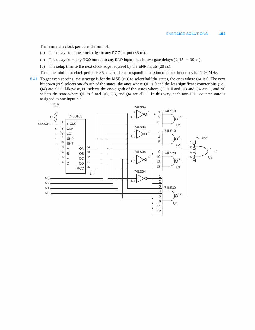
The minimum clock period is the sum of:
(a) The delay from the clock edge to any RCO output (35 ns).
(b) The delay from any RCO output to any ENP input, that is, two gate delays ( ).
(c) The setup time to the next clock edge required by the ENP inputs (20 ns).
Thus, the minimum clock period is 85 ns, and the corresponding maximum clock frequency is 11.76 MHz.
8.41 To get even spacing, the strategy is for the MSB (N3) to select half the states, the ones where QA is 0. The nextbit down (N2) selects one-fourth of the states, the ones where QB is 0 and the less significant counter bits (i.e.,QA) are all 1. Likewise, N1 selects the one-eighth of the states where QC is 0 and QB and QA are 1, and N0selects the state where QD is 0 and QC, QB, and QA are all 1. In this way, each non-1111 counter state isassigned to one input bit.
2 15⋅ 30 ns=
14
74LS163
CLR
Z
CLK
LD
QA
N3
N2
N1
N0
QB
2
11
1
9
ENP
ENT
7
10
A
B
3
4
CD
5
6QC
QD15RCO
U1
13
12
CLOCK
+5 V
R
74LS201
2
4
5
6
U3
12 12
13U2
74LS10
34 6
5U2
74LS10
1 2
U5
74LS04
3 4
U5
U5
74LS04
5 6
74LS04
123456
1112
12
U4
74LS30
910
81213 U3
74LS20
U5
74LS04

154 DIGITAL CIRCUITS
8.53--Chris Dunlap
--Xilinx Applications
library IEEE;
use IEEE.std_logic_1164.all;
use IEEE.std_logic_arith.all;
use IEEE.std_logic_unsigned.all;
entity v74x163s is
generic(size : integer := 8); --added generic
port (clk,clr_l,ld_l,enp,ent : in std_logic;
d : in std_logic_vector (size-1 downto 0); --changes range of input
q : out std_logic_vector (size-1 downto 0); --changes range of output
rco : out std_logic);
end v74x163s;
architecture v74x163_arch of v74x163s is
component synsercell is
port (clk, ldnoclr, di, coclrorld,cntenp,cnteni : in std_logic;
qi,cnteni1 : out std_logic);
end component;
signal ldnoclr,noclrorld : std_logic;
signal scnten : std_logic_vector (size downto 0); --creates a ranged temp with overflow room
begin
ldnoclr <= (not ld_l) and clr_l;
noclrorld <= ld_l and clr_l;
scnten(0) <= ent;
rco <= scnten(size);
gi: for i in 0 to size-1 generate --counts for size of counter
U1: synsercell port map (clk, ldnoclr, noclrorld, enp, d(i), scnten(i), scnten(i+1), q(i));
end generate;
end v74x163_arch;

EXERCISE SOLUTIONS 155
8.54 --**********************************
-- PROBLEM : WAKERLY - 8.54
-- FILES :
-- 8_54_top.vhd : top level file
-- 8_54_par2ser.vhd : parallel to serial converter
-- 8_54_control.vhd : control module
-- 8_54_shift_synch.vhd : 8 bit shift register
--
-- DESCRIPTION :
-- Creates a parallel to serial converter.
-- Data in is described as 8 x 8bit modules,
-- with a single 8 bit data bus that carries
-- data of the format given in Figure 8-55.
-- Each serial link has its own SYNCH(i) line;
-- the pulses should be staggered so SYNCH(i+1)
-- occurs 1 clock cycle after SYNCH(i).
--
-- Because of this, the load_synch line should
-- also be staggered so the data transmitted
-- over the serial link will correspond to its
-- associated SYNCH line.
--**********************************
-- library declarations
library IEEE;
use IEEE.std_logic_1164.all;
-- top level entity declaration
entity wak_8_54_top is
port (
data: in STD_LOGIC_VECTOR (63 downto 0);
clock: in STD_LOGIC;
synch: buffer STD_LOGIC_VECTOR (7 downto 0);
sdata: out STD_LOGIC_VECTOR (7 downto 0)
);
end wak_8_54_top;
architecture wak_8_54_arch of wak_8_54_top is
signal load_shift_master: std_logic;
signal synch_master: std_logic;
signal load_shift: std_logic_vector (7 downto 0);
--component declarations
component par2ser is
port (
clock: in STD_LOGIC;
data: in STD_LOGIC_VECTOR (7 downto 0);
load_shift: in STD_LOGIC;
sdata: out STD_LOGIC
);
end component;

156 DIGITAL CIRCUITS
component control is
port (
clock: in STD_LOGIC;
load_shift: out STD_LOGIC;
synch: out STD_LOGIC
);
end component;
component shift_synch is
port (
clock: in STD_LOGIC;
synch_in: in STD_LOGIC;
synch: buffer STD_LOGIC_VECTOR (7 downto 0)
);
end component;
begin
--component instantiations
S1: shift_synch port map (clock=>clock, synch_in=>synch_master, synch=>synch);
S2: shift_synch port map (clock=>clock, synch_in=>load_shift_master,
synch=>load_shift);
U1: par2ser port map (clock=>clock, data=>data(7 downto 0), load_shift=>load_shift(0),
sdata=>sdata(0));
U2: par2ser port map (clock=>clock, data=>data(15 downto 8),
load_shift=>load_shift(1), sdata=>sdata(1));
U3: par2ser port map (clock=>clock, data=>data(23 downto 16),
load_shift=>load_shift(2), sdata=>sdata(2));
U4: par2ser port map (clock=>clock, data=>data(31 downto 24),
load_shift=>load_shift(3), sdata=>sdata(3));
U5: par2ser port map (clock=>clock, data=>data(39 downto 32),
load_shift=>load_shift(4), sdata=>sdata(4));
U6: par2ser port map (clock=>clock, data=>data(47 downto 40),
load_shift=>load_shift(5), sdata=>sdata(5));
U7: par2ser port map (clock=>clock, data=>data(55 downto 48),
load_shift=>load_shift(6), sdata=>sdata(6));
U8: par2ser port map (clock=>clock, data=>data(63 downto 56),
load_shift=>load_shift(7), sdata=>sdata(7));
U9: control port map (clock=>clock, load_shift=>load_shift_master,
synch=>synch_master);
end wak_8_54_arch;

EXERCISE SOLUTIONS 157
--*************************************
-- Basically an 8-bit shift register
-- takes the synch_in signal as an
-- input, and outputs an 8 bit signal,
-- each consecutive bit delayed by one
-- from the previous bit.
-- library declaration
library IEEE;
use IEEE.std_logic_1164.all;
use IEEE.std_logic_arith.all;
use IEEE.std_logic_unsigned.all;
-- top level entity declaration
entity shift_synch is
port (
clock: in STD_LOGIC;
synch_in: in STD_LOGIC;
synch: buffer STD_LOGIC_VECTOR (7 downto 0)
);
end shift_synch;
architecture shift_synch_arch of shift_synch is
begin
-- low order synch signal is simply passed through
-- to output. all others are delayed.
synch(0) <= synch_in;
process(clock)
begin
if clock'event and clock='1' then
for I in 0 to 6 loop
synch(I+1) <= synch(I);
end loop;
end if;
end process;
end shift_synch_arch;

158 DIGITAL CIRCUITS
--***************************************
-- Parallel to serial converter
-- Data is entered through 8 bit DATA bus
-- It is loaded into the register when
-- load_shift is low. If load_shift is
-- high, shift data serially out through sdata
-- library declarations
library IEEE;
use IEEE.std_logic_1164.all;
-- top level entity declaration
entity par2ser is
port (
clock: in STD_LOGIC;
data: in STD_LOGIC_VECTOR (7 downto 0);
load_shift: in STD_LOGIC;
sdata: out STD_LOGIC
);
end par2ser;
architecture par2ser_arch of par2ser is
-- internal signal declaration
signal REG: STD_LOGIC_VECTOR(7 downto 0);
signal DIN: std_logic;
begin
-- DIN <= 0 will set the high order bit to be
-- zero once data is loaded in.
DIN <= '0';
-- process to create shift register
--accomplished by simply taking the DIN signal
--and concatenating on the end the previous
--6 high order bits.
process (clock)
begin
if clock'event and clock='1' then
if load_shift = '0' then
REG <= data;
else
REG <= DIN & REG(7 downto 1);
end if;
end if;
sdata <= REG(0);
end process;
end par2ser_arch;

EXERCISE SOLUTIONS 159
8.55 This is really the second paragraph of Exercise 8.54.
--******************************
-- Control logic
-- controls the loading of the
-- parallel to serial shift register
-- through the load_shift signal.
-- also, controls the synch word.
-- this occurs every 256 clock cycles.
--library declaration
library IEEE;
use IEEE.std_logic_1164.all;
use IEEE.std_logic_arith.all;
use IEEE.std_logic_unsigned.all;
--top level entity declaration
entity control is
port (
clock: in STD_LOGIC;
load_shift: out STD_LOGIC;
synch: out STD_LOGIC
);
end control;
architecture control_arch of control is
--internal signal declaration
signal COUNT: STD_LOGIC_VECTOR(7 downto 0);
signal load: STD_LOGIC;
begin
load <= '0'; --define constant
process (clock)
begin
if clock'event and clock='1' then
count <= count + 1;
if count(2 downto 0) = "110" then
load_shift <= load;
else
load_shift <= not load;
end if;
if count = 254 then
synch <= '1';
else
synch <= '0';
end if;
end if;
end process;
end control_arch;

160 DIGITAL CIRCUITS
8.62 Regardless of the number of shift-register outputs connected to the odd-parity circuit, its output in state 00...00is 0, and the 00...00 state persists forever. However, suppose that an odd number of shift-register outputs areconnected. Then the output of the odd-parity circuit in state 11...11 is 1, and the 11...11 state also persists for-ever. In this case, the number of states in the “maximum-length” sequence can be no more than , sincetwo of the states persist forever. Therefore, if an LFSR counter generates a sequence of length , it musthave an even number of shift-register outputs connected to the odd-parity circuit.
8.64 The figure below shows the effect of physically changing the odd-parity circuit to an even-parity circuit (i.e.,inverting its output).
From Exercise 9.32, we know that an even number of shift-register outputs are connected to the parity circuit,and we also know that complementing two inputs of an XOR gate does not change its output. Therefore, we canredraw the logic diagram as shown below.
2n 2–2n 1–
N-bitparallel-outshift register
PR
CLK
SERIN
QB
QA
QC
QY
QX
QZ
CLOCK
RESET_L
XN_L
connect toselected outputs
(see table)
even-parity circuit
XN–1
XN–2
XN–3
X2
X1
X0
N-bitparallel-outshift register
PR
CLK
SERIN
QB
QA
QC
QY
QX
QZ
CLOCK
RESET_L
XN_L
connect toselected outputs
(see table)
even-parity circuit
XN–1
XN–2
XN–3
X2
X1
X0

EXERCISE SOLUTIONS 161
Finally, we can move the inversion bubbles as shown below.
This circuit has exactly the same structure as Figure 8–68, except that the shift register stores complementeddata. When we look at the external pins of the shift register in the first figure in this solution, we are looking atthat complemented data. Therefore, each state in the counting sequence of the even-parity version (our firstfigure) is the complement of the corresponding state in the odd-parity version (Figure 8–68). The odd-parityversion visits all states except 00...00, so the even-parity version visits all states except 11...11.
N-bitparallel-outshift register
CLR
CLK
SERIN
QB
QA
QC
QY
QX
QZ
CLOCK
RESET_L
XN
connect toselected outputs
(see table)
odd-parity circuit
XN–1
XN–2
XN–3
X2
X1
X0

162 DIGITAL CIRCUITS
8.68 --Johnny West
--Xilinx Applications
--8.68 : Design an iterative circuit for checking the parity of a 16-bit data
-- word with a single even-parity bit.
------------------------------------------------------------------------------------
------------
--This portion of the code constructs the iterative module that will cascaded 16
--times in order to check the parity of a 16 bit word.
------------------------------------------------------------------------------------
------------
library IEEE;
use IEEE.std_logic_1164.all;
--Generic Iterative Module
entity Iterative_Module is
port (
carry_in, primary_in: in STD_LOGIC;
carry_out: out STD_LOGIC
);
end Iterative_Module;
--An XOR is performed on the current parity of a word (carry_in) and the
--next bit in the word (boundary_in)
--Even parity produces a 0 and odd parity produces a 1
architecture Parity_Check of Iterative_Module is
begin
carry_out <= carry_in xor primary_in;
end Parity_Check;

EXERCISE SOLUTIONS 163
8.75 In the following design, RESET is not recognized until the end of phase 6. RESTART is still recognized at theend of any phase; otherwise it would have no real use (i.e., only going back to phase 1 after the end of phase 6,
-----------------------------------------------------------------------------------
--This portion of the code cascades the interative module 16 times and connects the
--modules together.
-----------------------------------------------------------------------------------
library IEEE;
use IEEE.std_logic_1164.all;
--Top level entity for checking the parity of a 16bit word
entity Parity_16bit is
port (data_word: in STD_LOGIC_VECTOR (15 downto 0);
parity: out STD_LOGIC );
end Parity_16bit;
--Architecture consists of 16 cascaded iterative modules
architecture Parity_16bit_arch of parity_16bit is
component Iterative_Module
port (carry_in, primary_in: in STD_LOGIC;
carry_out: out STD_LOGIC );
end component;
signal carry: STD_LOGIC_VECTOR (15 downto 0);
signal cin0: STD_LOGIC;
begin
cin0 <= '0';
P0: Iterative_Module port map (cin0, data_word(0), carry(0));
P1: Iterative_Module port map (carry(0), data_word(1), carry(1));
P2: Iterative_Module port map (carry(1), data_word(2), carry(2));
P3: Iterative_Module port map (carry(2), data_word(3), carry(3));
P4: Iterative_Module port map (carry(3), data_word(4), carry(4));
P5: Iterative_Module port map (carry(4), data_word(5), carry(5));
P6: Iterative_Module port map (carry(5), data_word(6), carry(6));
P7: Iterative_Module port map (carry(6), data_word(7), carry(7));
P8: Iterative_Module port map (carry(7), data_word(8), carry(8));
P9: Iterative_Module port map (carry(8), data_word(9), carry(9));
P10: Iterative_Module port map (carry(9), data_word(10), carry(10));
P11: Iterative_Module port map (carry(10), data_word(11), carry(11));
P12: Iterative_Module port map (carry(11), data_word(12), carry(12));
P13: Iterative_Module port map (carry(12), data_word(13), carry(13));
P14: Iterative_Module port map (carry(13), data_word(14), carry(14));
P15: Iterative_Module port map (carry(14), data_word(15), carry(15));
parity <= carry(15); --parity = 0 is even parity and 1 if odd parity
end parity_16bit_arch;

164 DIGITAL CIRCUITS
which happens anyway.) Presumably, RESTART would be used only with great care or in unusual circum-stances (e.g., during debugging).
8.81 This problem can be a bit confusing since the states in Table 7–14 have the same names as the ’163 data inputs.Therefore, we shall use the names SA, SB, and so on for the states.
The idea is to normally allow the counter to count to the next state, but to force it to go to SA or SB when thewrong input is received. The CLR_L input is used to go to SA (0000), and the LD_L input is used to go to SB(0001; the counter’s A–D data inputs are tied LOW and HIGH accordingly).
Inspecting the state table on page 582 of the text, we see that state A should be loaded when X=1 and themachine is in state SA, SD, or SH. Thus,
All of the other next-states when X=1 are the natural successors obtained by counting.
Similarly, state SB should be loaded when X=0 and the machine is in state SB, SC, SE, SF, or SH. In addition,notice that in state SG, the next state SE is required when X=0; the load input must be used in this case too, buta different value must be loaded. Thus, LD_L will be asserted in six of the eight states when X=0.
Optionally, LD_L could be easily asserted in the remaining two states as well, since the required next states (SBand SE) are ones that we must generate in other six cases anyway. Thus, we can connect X to the LD_L input, sowe always load when X=0. Then, we load either SB (0010) or SE (0100) depending on the current state. There-fore, we can write the following equations for data inputs A–D:
Alternatively, we could realize C as an AND-OR circuit and complement to get B:
module TIMEGEN6 title 'Six-phase Master Timing Generator'
" Input and Output pins MCLK, RESET, RUN, RESTART pin;T1, P1_L, P2_L, P3_L, P4_L, P5_L, P6_L pin istype 'reg';
" State definitionsPHASES = [P1_L, P2_L, P3_L, P4_L, P5_L, P6_L];NEXTPH = [P6_L, P1_L, P2_L, P3_L, P4_L, P5_L];SRESET = [1, 1, 1, 1, 1, 1];P1 = [0, 1, 1, 1, 1, 1];P6 = [1, 1, 1, 1, 1, 0];
equationsT1.CLK = MCLK; PHASES.CLK = MCLK;
WHEN (RESET & PHASES==P6 & !T1) THEN {T1 := 1; PHASES := SRESET;}ELSE WHEN (PHASES==SRESET) # RESTART THEN {T1 := 1; PHASES := P1;}ELSE WHEN RUN & T1 THEN {T1 := 0; PHASES := PHASES;}ELSE WHEN RUN & !T1 THEN {T1 := 1; PHASES := NEXTPH;}ELSE {T1 := T1; PHASES := PHASES;}
end TIMEGEN6
CLR_L X Q( C ′ QB′ QA ′⋅ ⋅ ⋅ QC ′ QB QA⋅ ⋅ QC QB QA )⋅ ⋅+ +[ ]′=
X Q( C ′ QB′ QA⋅ ⋅ ⋅ QB QA )⋅+[ ]′=
A 0=
B SA SB SC SE SF SH+ + + + +=
QB ′ QC′ QA ′⋅ QC QA⋅+ +=
C B ′=
D 0=
C QC′ QB QA⋅ ⋅ QC QB QA′⋅ ⋅+=
B C′=

EXERCISE SOLUTIONS 165
The logic diagram follows directly from these equations. The output logic can be realized using the equationson page 584 of the text.
8.90 Transitions on SYNCIN occur a maximum of 20 ns after the rising edge of CLOCK. Given a 40-ns clock periodand a 10-ns setup-time requirement for the other ’ALS74s, 10 ns is the maximum propagation delay of thecombinational logic.