classical optics in a new light: flat photonics based on · pdf file ·...
TRANSCRIPT

Federico Capasso
Harvard School of Engineering and Applied Sciences
Zeiss Lecture, Jena March 7, 2013
1
Classical Optics in a New Light:
Flat Photonics based on Metasurfaces
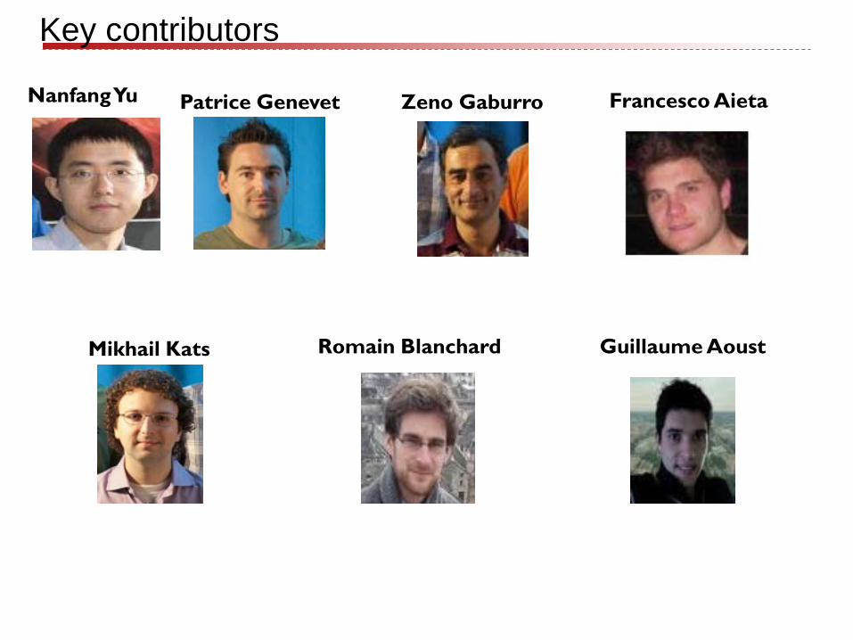
Nanfang Yu Zeno Gaburro
Romain Blanchard
Guillaume Aoust
Patrice Genevet
Mikhail Kats
Francesco Aieta
Key contributors

Recent developments in field of optics
Metamaterials and Transformation Optics
Viktor G Veselago 1968 Sov. Phys. Usp. 10 509 A.J. Ward and J.B. Pendry, J. Mod. Opt. 43 (1996) J.B. Pendry, D. Schurig and D.R. Smith, Science 312, 1780 (2006) Optical cloaking
Propagation of light is controlled by considering artificial 3D materials with designed permittivity and permeability.
What can we do in 2D ? “metasurfaces”
Negative refraction

• Planar technology is central to Integrated Circuit technology ( $ 300 B industry):
Technology platform.
• Because of fabrication complexity 3D optical materials (metamaterials etc.) don’t
have a good chance of a major technology impact at optical wavelengths.
• Lessons of photonic (PC) crystals: beautiful physics but very limited technology penetration due to fabrication complexity\
So we should look at what we can do in 2D with metasurfaces:
METASURFACES FOR FLAT OPTICS • Optically thin engineered metasurfaces for Wave Front Engineering (phase control): • Refractive index is not a useful quantity when we think about metasurfaces: local
phase and amplitude control of light along the surface using optical antennas
• New class of flat, compact and broadband components:(lenses, polarizers, etc.), be-
yond conventional diffractive optics
Optical phased arrays for high speed wavefront control
The Vision of Flat Optics with Metasurfaces
5
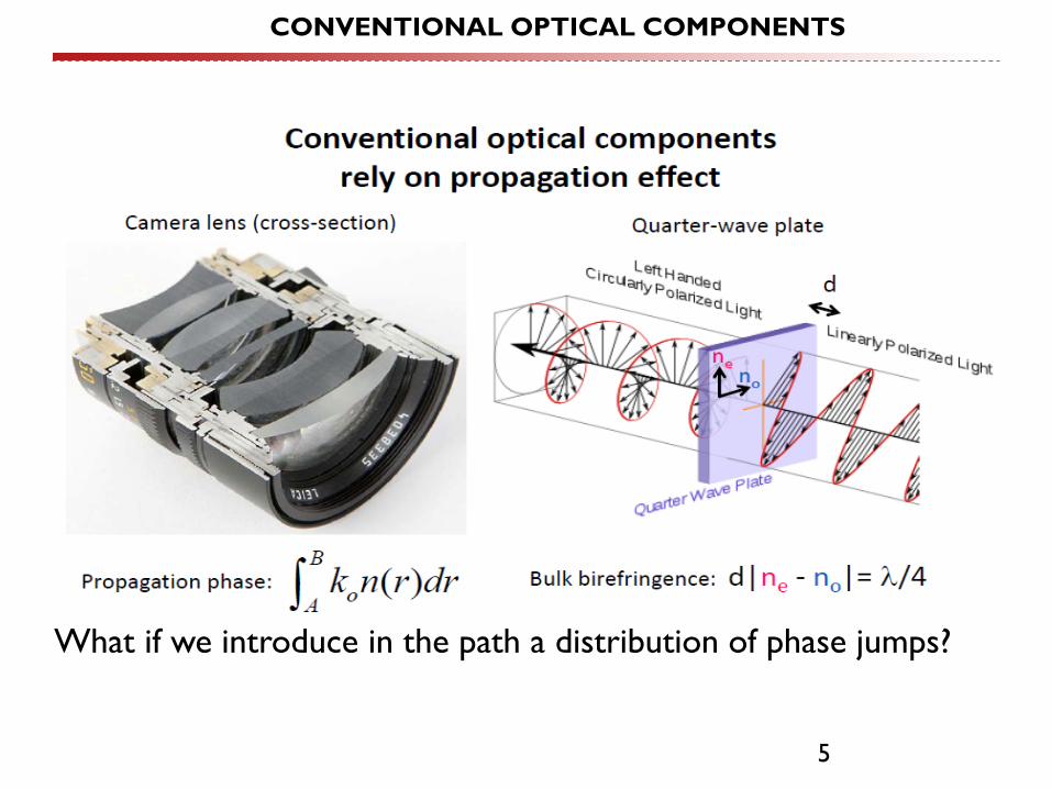
What if we introduce in the path a distribution of phase jumps?
CONVENTIONAL OPTICAL COMPONENTS

How to impart an abrupt phase profile to a wavefront
Requirements : - deep subwavelength thickness - subwavelength separation
- - 2 π phase coverage
- - high and uniform scattering amplitude
-Flat (2D) photonic components: - Lenses and Axicons - - Polarizers
- -Vortex plates - =optical phased arrays
By using subwavelenth optical resonators on a metasurface with suitably designed geometry in order to scatter light with the desired
phase distribution
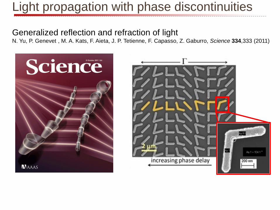
Light propagation with phase discontinuities
Generalized reflection and refraction of light N. Yu, P. Genevet , M. A. Kats, F. Aieta, J. P. Tetienne, F. Capasso, Z. Gaburro, Science 334,333 (2011)
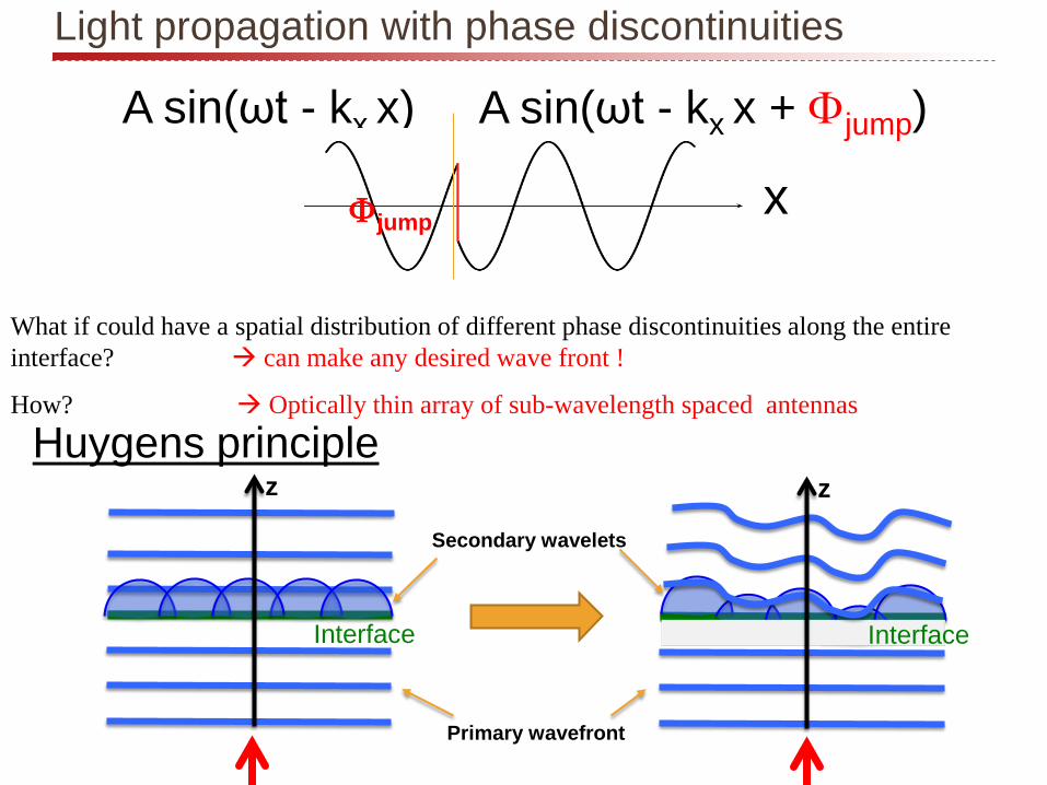
A sin(ωt - kx x)
x
A sin(ωt - kx x + Φjump)
Φjump
Secondary wavelets
Primary wavefront
Interface
z
Interface
z Huygens principle
Light propagation with phase discontinuities
What if could have a spatial distribution of different phase discontinuities along the entire interface? can make any desired wave front !
How? Optically thin array of sub-wavelength spaced antennas

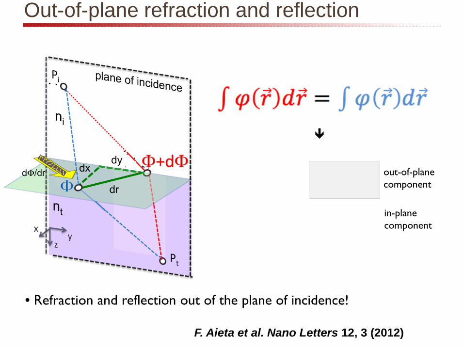
Fermat’s principle: Imposing the stationary phase conditions: konidxSin(θi) +(Φ+dΦ) = kontdxSin(θt)+Φ
Generalized reflection and refraction of light Suppose interface with a constant gradient of phase delay
dΦ/dx
Similarly for reflection:
Generalized Snell’s law

Reflection and refraction from a metasurface
10
Optically thin: 50nm Subwavelength phase resolution: ~λ/5 Instant imprinting of a linear phase distribution
anomalous reflection
anomalous refraction
λ = 8 µm
incident wave
silicon
N. Yu et al., Science 334, 333 (2011)
3 4 5 6 7 8 9
-0.5
0
0.5
1
Wavelength (µm)
Phas
eπ
3 4 5 6 7 8 90
0.2
0.4
0.6
0.8
1
Scat
terin
g In
tens
ity (a
.u.)
Wavelength (µm)
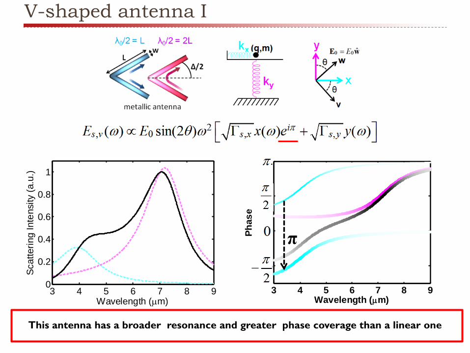
V-shaped antenna I
This antenna has a broader resonance and greater phase coverage than a linear one

V-Shape Antenna II
π/4 0 7π/4 6π/4 5π/4 4π/4 3π/4 2π/4
✓ uniform amplitude ✓ 2π phase coverage

-45o
0o
45o
90o
-45o 0o 45o 90o 135o 180o 225o 270o
Eight-element unit cell: full 2 π coverage with equal scattering amplitude
Mirror structure

Anomalous refraction
The antenna operate as secondary scatterers with a tailorable phase response, re-directing a normally-incident beam away from the normal
Uniform scattering amplitude Controlled phase responses between 0 to 2π
Arrays of Au antennas on Silicon

Experimental results: anomalous refraction
N. Yu et al. Science 334,333 (2011)
Γ
• Linear gradient of phase discontinuities creates modified refraction and reflection behavior
θt = arcSin(- λo/Γ)

Anomalous reflection and refraction
- Negative reflection - Nonlinear relationship - Critical angle for reflection
- Negative refraction - New total internal reflection angles
Reflection Refraction

Reflected and refracted beams
ordinary refraction
incidence λ= 8µm
ordinary reflection
anomalous refraction
anomalous reflection
iθ
silicon
~10% ~20%
~20%
~40%
antenna absorption ~10%

in-plane component
out-of-plane component
F. Aieta et al. Nano Letters 12, 3 (2012)
• Refraction and reflection out of the plane of incidence!
Out-of-plane refraction and reflection
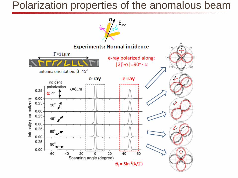
Polarization properties of the anomalous beam
â ŝ Einc
α

Incident wave
e-ray (scattered
light)
Quarter wave plate
o-ray (background
)
Design based on phased optical antennas Background free
Arbitrary orientation of incident E-field vector
Broadband operation: quarter-wave plate ∆λ=5-14µm
2 µm

z
x
y
45o
Einc π/8
Ea Eb d π/8
3π/8
3π/8
45o
Unit a
Unit b
Creating beams with arbitrary polarization
The two rows of antennas in the unit cell create the two orthogonal polarized components with 90 degree phase difference
d = Γ/4 ↔ Ψ = π/2
P=E×H
Propagation direction
Poynting vector
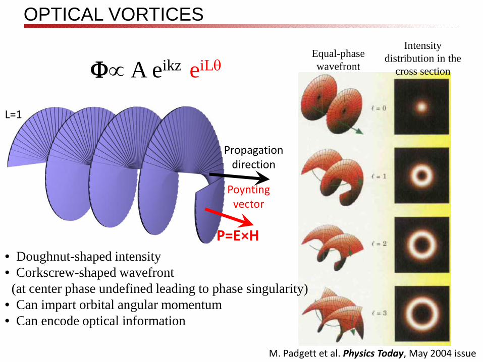
OPTICAL VORTICES
Φ∝ A eikz eiLθ
L=1
M. Padgett et al. Physics Today, May 2004 issue
Intensity distribution in the
cross section
Equal-phase wavefront
• Doughnut-shaped intensity • Corkscrew-shaped wavefront (at center phase undefined leading to phase singularity) • Can impart orbital angular momentum • Can encode optical information
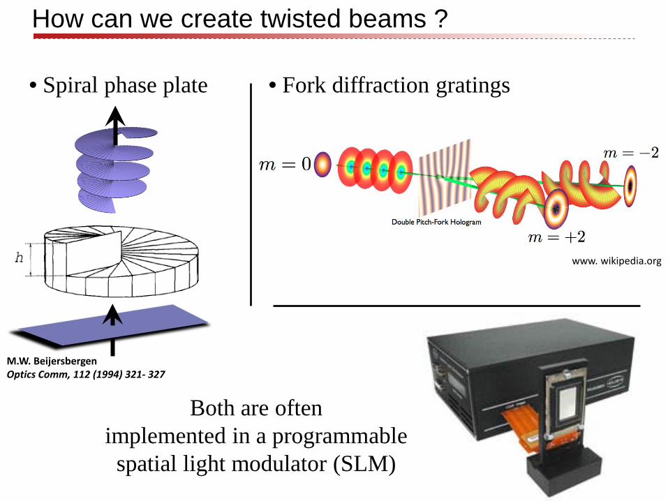
How can we create twisted beams ?
• Spiral phase plate
M.W. Beijersbergen Optics Comm, 112 (1994) 321- 327
Both are often implemented in a programmable spatial light modulator (SLM)
• Fork diffraction gratings
www. wikipedia.org
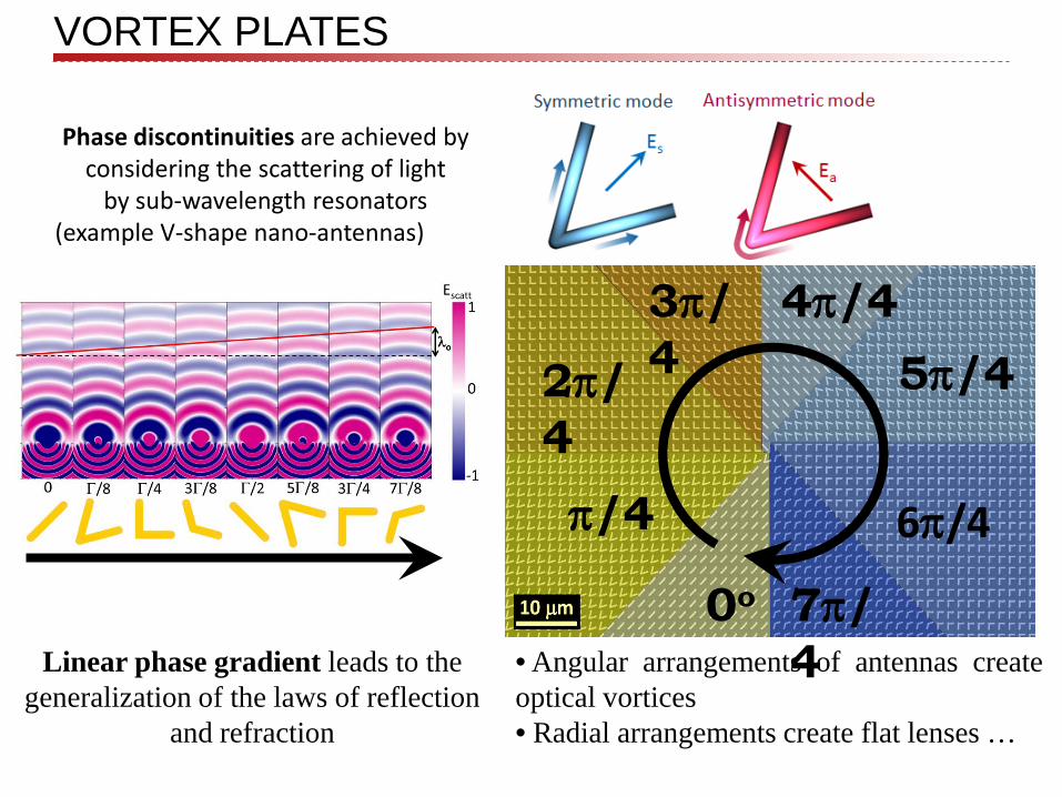
VORTEX PLATES
Linear phase gradient leads to the generalization of the laws of reflection
and refraction
Phase discontinuities are achieved by considering the scattering of light
by sub-wavelength resonators (example V-shape nano-antennas)
Go beyond the basics manipulation of
reflection and refraction of light ?
6π/4
5π/4
4π/4 3π/4
2π/4
π/4
0o 7π/4 • Angular arrangements of antennas create
optical vortices • Radial arrangements create flat lenses …
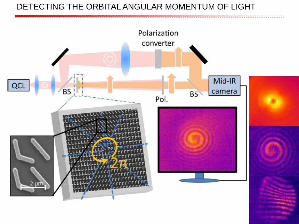
DETECTING THE ORBITAL ANGULAR MOMENTUM OF LIGHT

How can we detect those twisted light beams?
Intersection between the two wavefronts follows a spiral line

L=1
How can we detect those twisted light beams?
Intersection between the two wavefronts
Dislocated fringe

Generation of multi-charged vortex beam
20 µm
2π -2π
-4π 4π 20 µm

WHAT’S THE BIG DEAL ?
Amplitude
Phase
0.2 µm 1 µm 2 µm 3.5 µm 8 µm
Distance from interface
Desired phase distribution is imprinted on the incident wavefront at the interface.

n1 n2
Why Lenses are thick ? Can we make a flat lens
Propagating Wavefront

Flat Lens
To focus at a certain focal f the interface must compensate for the distance of every point from a spherical surface centered in the focus and with radius f.
F. Aieta et al Nanoletters ,Aug. 15 , 2012 (on line)
No spherical aberration and large numerical aperture
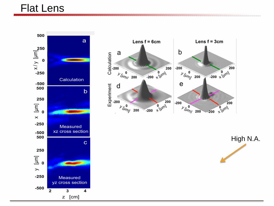
Flat Lens
High N.A.

No Spherical Aberration for flat lens
sinϑi ≠ ϑi High N.A. = 0.8
Wavefront = Envelope of Secondary Waves with radii R(x) = λ/2π *φ(x)
x z
Metasurface
φ(x) -0.5 0.5 -0.5 0.5 0 x/f x/f 0
Spherical Hyperboloidal
Lens
φ(x)

Flat Lens
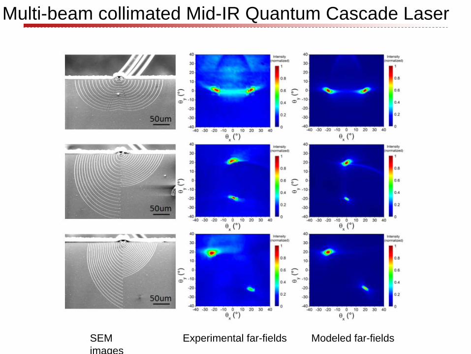
Multi-beam collimated Mid-IR Quantum Cascade Laser
SEM images
Experimental far-fields Modeled far-fields

Diffractive optics based on metasurfaces
• Technology simplification: a single digital pattern (one mask level) creates arbitrary analog phase profile • Lithography: nanoimprint and soft lithography

Thin film optical coatings Last half century: a lot of work on optical coatings and filters using thin film
interference effects
Nearly all thin film optical coatings use dielectric layers with thickness on the order of a wavelength, where the dielectrics have low optical loss

Thin film interference: Coloring by reflection resonance in λ/4 thick films

Nanometer thickness optical coatings We were able to make “blue gold”, “pink gold”, and other colors
utilizing 5-20 nm semiconductor layers much thinner than λ/4
Polished substrate
Rough substrate (still works!)
Kats et al, Nature Materials (published online, 2012)
Bare Au
Au + 7nm Ge
Au + 15nm Ge

Nanometer thickness optical coatings Patterning ultra-thin coatings to create images, labels, etc
The difference between blue and purple, and purple and pink is only ~4 nm of germanium (~ 8 atomic layers)!
Kats et al, Nature Materials (published online, 2012)

Reflection phase shifts at dielectric-dielectric interfaces are either 0 or π and reflection from an ideal metal has π phase shift
Metals with finite conductivity and lossy dielectrics have “weird” interface reflection phase shifts (i. e. not 0 or π) Resonances can exist for films significantly thinner than λ/(4n)
To achieve high absorption, the dielectric must be very lossy
Punchline: it is possible to have an absorption resonance at specific wavelength (and even a perfect absorber) resulting from coherent effects in a system involving an ultra-thin, highly-lossy layer
This leads to coloring
Im[r]
Re[r] h << λ/4n
r0
r1 r2
r3
Absorption resonance in ultrathin (<< λ) highly absorbing films

Absorption resonances lead to coloring
Lossy dielectric Germanium Lossy metal Gold
Ellipsometry Experiment
Calculation Calculation

Physical concept
Why was this simple geometry be overlooked? 1. Coherent effects are not discussed in highly-lossy materials 2. Without lossy materials, reflection phase shifts are fixed to
either 0 or π
Lossy materials introduce nontrivial reflection phase shifts (> π) Resonant cavities can be made thinner than λ/4 Short propagation lengths allow the use of highly
absorbing media
π
n1 < n2
0
n2 > n1 n1 PEC
π
n1
??
2n

Ultra-thin perfect absorber
To appear in Nov. 26 issue of Applied Physics Letters
M. Kats, D. Sharma, J. Lin, P. Genevet, R. Blanchard, Z. Yang, M. Qazilbash, D. Basov, S. Ramanathan, F. Capasso, “Ultra-thin perfect absorber using a tunable phase change material”
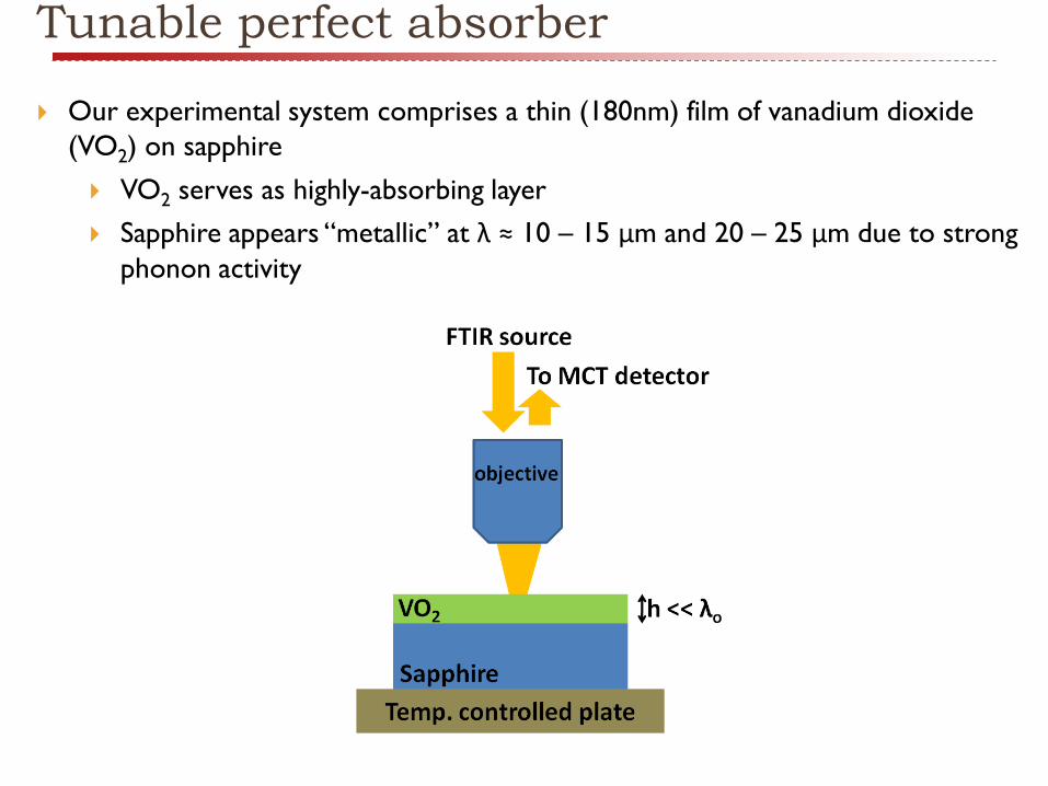
Tunable perfect absorber
Our experimental system comprises a thin (180nm) film of vanadium dioxide (VO2) on sapphire VO2 serves as highly-absorbing layer Sapphire appears “metallic” at λ ≈ 10 – 15 μm and 20 – 25 μm due to strong
phonon activity

Vanadium dioxide (VO2) VO2 is a correlated metal oxide which experiences phase change upon heating
to past ~70 °C (reversible, but with hysteresis) Conductivity changes by >10,000 from the insulating to conducting state
Transition can be triggered thermally, optically, and electrically Ongoing research to make various electronic devices (switches, etc) with VO2
Yang et al, Ann. Rev. Mat. Res. (2011)

VO2 in the transition region
What happens in the transition state of VO2?
Nanoscale islands of metal-phase VO2 begin to form within a background of dielectric-phase VO2, which then grow and connect The mixture can be viewed as a disordered, natural metamaterial
The ratio of co-existing phases can be controlled tunable medium
Qazilbash, Basov, et al, Science (2007)

Tunable perfect absorber
Temperature control of VO2 allows us to significantly change the sample reflectivity!
Reflectivity tuning from ~80% to 0.25% at 11.6um on off ratio of more than 300 entire effect due to just 180nm of VO2 on sapphire
5 10 150
0.2
0.4
0.6
0.8
1
Wavelength (µm)
Ref
lect
ivity
297K343K346K347K348K351K360K

Tunable perfect absorber
Used textbook 3-layer equation
5 10 150
0.2
0.4
0.6
0.8
1
Wavelength (µm)
Ref
lect
ivity
297K343K346K347K348K351K360K
5 10 150
0.2
0.4
0.6
0.8
1normal incidence, 180nm VO2
Wavelength (µm)
Ref
lect
ivity
295K341K342K343K343.6K346K360K
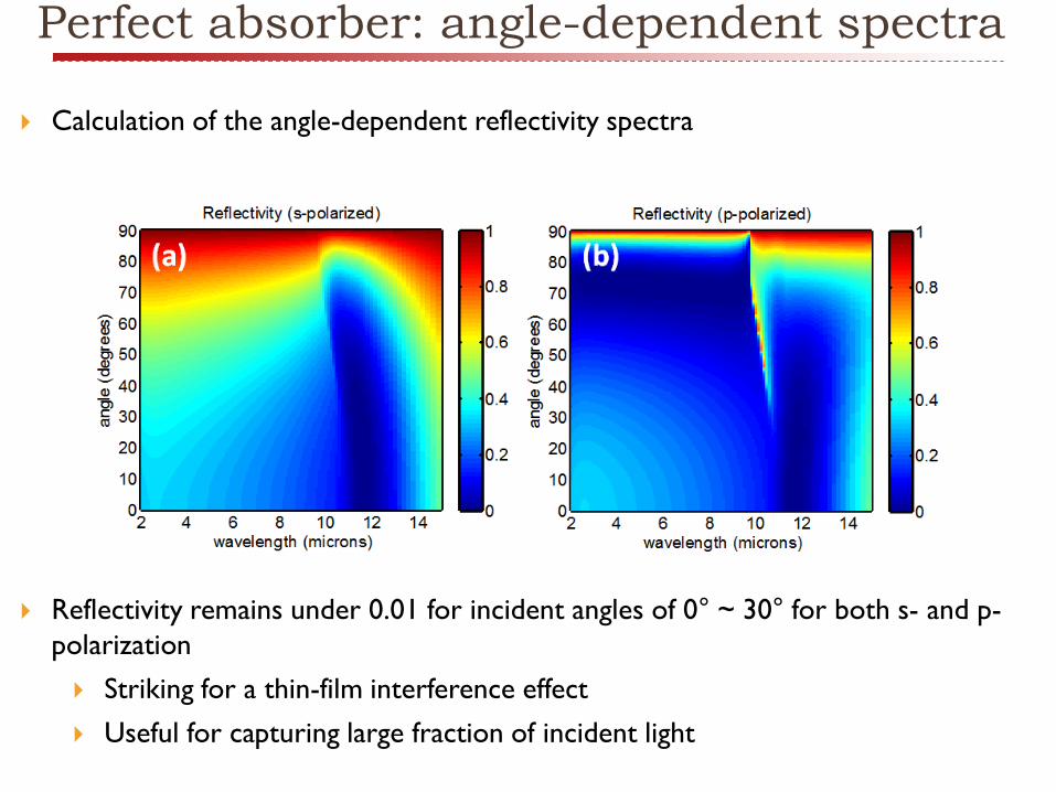
Perfect absorber: angle-dependent spectra
Calculation of the angle-dependent reflectivity spectra
Reflectivity remains under 0.01 for incident angles of 0° ~ 30° for both s- and p- polarization Striking for a thin-film interference effect Useful for capturing large fraction of incident light

Perspectives: ultra-thin optical coatings
Coloring of metals Smooth and rough metals can be colored by application of ultra-
thin, highly-absorbing films
Modifying reflectivity for optical applications Very black surfaces Reshaping ultra-fast pulses
Patterning colors
New, ultra-flat, single-material labels and patterns
Harnessing the absorption Ultra-thin angle-insensitive photodetectors, solar cells, etc Can use semiconductors or semiconducting polymers

Flat optics
High NA Objective
Non-Invasive Imaging for Biomedical Application
Major opportunity in Midir due to
poor refractory materials
Smart Phones
StrechableMaterials
• Lithography: from Optical to Nanoimprinting and Soft Lithography
• New class of flat, compact and broadband components: lenses, polarizers., filters,
High speed tunable phased array for real-time wavefront control

Thank you!
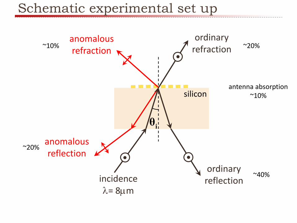
Schematic experimental set up
ordinary refraction
incidence λ= 8µm
ordinary reflection
anomalous refraction
anomalous reflection
iθ
silicon
~10% ~20%
~20%
~40%
antenna absorption ~10%