class d amp
DESCRIPTION
Class D amp whitepapersTRANSCRIPT

Project Number: JKM-2A03
Class-D Audio Amplifier
A Major Qualifying Report:
submitted to the Faculty
of the
WORCESTER POLYTECHNIC INSTITUTE
in partial fulfillment of the requirements for the
Degree of Bachelor of Science
by
______________________________________________ Alex C. DiDonato
______________________________________________ Ryan T. Dupuis
______________________________________________ Tyler W. Folsom
Date: April 29, 2004
Approved:
__________________________________________ __________________________________________Professor John McNeill
Project Advisor Professor Demetrios Papageorgiou
Project Advisor
1

ABSTRACT
This MQP involved the design, construction, and testing of an Ultra-Efficient, High-Powered, Class-D
audio amplifier. The main goal was to achieve 95% efficiency using the 42 Volt PowerNet Standard.
The signal processing stage was completed using a three-level Sigma-Delta Modulation scheme which
powered a MOSFET H-Bridge configuration. Testing confirmed that the goal of 95% efficiency was
met, and an RMS power of 400 Watts was produced using a 42 Volt supply.
2

Acknowledgements
We would first like to thank Analog Devices, Texas Instruments, and Allegro Microsystems for
sponsoring the Analog MQP lab. Without their continued support, the resources needed to fund this
project would not have been available.
We would also like to thank all the companies that were willing to donate free samples for us to
perform testing in lab. These companies included Fairchild Semiconductor, Texas Instruments,
Intersil, and Analog Devices.
A huge thank you goes out to Tom Angelotti for all his patience and willingness to help us when we
needed anything from the shop.
The most thanks goes out to our MQP advisors Professor McNeill and Professor Papageorgiou for all
their guidance and support throughout the year. Without their willingness to always bestow their
knowledge and help when in dire need, our MQP would not have been a success.
3

TABLE OF CONTENTS
ABSTRACT ...............................................................................................................................................................................2 ACKNOWLEDGEMENTS ......................................................................................................................................................3 TABLE OF FIGURES ..............................................................................................................................................................5 EXECUTIVE SUMMARY .......................................................................................................................................................7 1 INTRODUCTION............................................................................................................................................................9 2 BACKGROUND ............................................................................................................................................................10
2.1 WHAT IS CLASS-D...................................................................................................................................................10 2.2 METHODS OF ACHIEVING CLASS-D.........................................................................................................................12
2.2.1 Pulse Width Modulation ....................................................................................................................................12 2.2.2 Sigma-Delta Modulation....................................................................................................................................15 2.2.3 Digital Signal Processing ..................................................................................................................................18
2.2.3.1 S/PDIF ....................................................................................................................................................................... 19 2.3 POWERNET 42V STANDARD....................................................................................................................................22 2.4 POWER MOSFETS ..................................................................................................................................................25 2.5 POTENTIAL CONCERNS............................................................................................................................................28
2.5.1 Filtering .............................................................................................................................................................28 2.5.2 Electromagnetic Interference (EMI) ..................................................................................................................32
2.6 EFFICIENCY .............................................................................................................................................................35 2.7 CONTROLS THEORY.................................................................................................................................................39 2.8 TEST MEASUREMENT METHODOLOGY ....................................................................................................................41
3 DESIGN ..........................................................................................................................................................................43 3.1 SIGMA DELTA MODULATION...................................................................................................................................43 3.2 POWER STAGE .........................................................................................................................................................48 3.3 SYSTEM STABILITY .................................................................................................................................................50 3.4 FILTER.....................................................................................................................................................................53 3.5 HEAT SINK...............................................................................................................................................................57 3.6 PRINTED CIRCUIT BOARD........................................................................................................................................59
4 PROJECT EVOLUTION..............................................................................................................................................62 4.1 FIRST PCB...............................................................................................................................................................62 4.2 SECOND PCB...........................................................................................................................................................63 4.3 THIRD PCB..............................................................................................................................................................65 4.4 FOURTH PCB...........................................................................................................................................................67
5 TESTING AND RESULTS ...........................................................................................................................................68 5.1 EFFICIENCY TESTING...............................................................................................................................................68 5.2 “DEAD-ZONE”.........................................................................................................................................................71 5.3 ACOUSTIC CLARITY.................................................................................................................................................75 5.4 OUTPUT POWER.......................................................................................................................................................76 5.5 SIGNAL TO NOISE RATIO .........................................................................................................................................78 5.6 EFFICIENCY LOSS ....................................................................................................................................................80
6 RECOMMENDATIONS...............................................................................................................................................88 7 CONCLUSIONS ............................................................................................................................................................90 8 REFERENCES...............................................................................................................................................................91 APPENDIX ..............................................................................................................................................................................92
4

Table of Figures Figure 1: Class-D explanation without modulation or brightness reduction ............................................ 10 Figure 2: Class-D explanation with resistor added to reduce brightness.................................................. 11 Figure 3: Switch Open .............................................................................................................................. 11 Figure 4: Switch Closed............................................................................................................................ 11 Figure 5: Input Sine Wave vs. PWM Output............................................................................................ 13 Figure 6: Two-Level vs. Three-Level PWM ............................................................................................ 14 Figure 7: PWM Comparator ..................................................................................................................... 15 Figure 8: Delta Modulation and Demodulation ........................................................................................ 16 Figure 9: Block Diagram of Sigma-Delta (Σ-∆) Modulation ................................................................... 17 Figure 10: DSP Block Diagram ................................................................................................................ 19 Figure 11: Biphase-Mark-Code Example ................................................................................................. 21 Figure 12: Maximum Over-voltage .......................................................................................................... 23 Figure 13: Maximum Dynamic Voltage ................................................................................................... 24 Figure 14: Starting Voltage....................................................................................................................... 25 Figure 15: H-Bridge.................................................................................................................................. 27 Figure 16: Typical Low-Pass Filter .......................................................................................................... 29 Figure 17: H-Bridge Output Low-Pass Filter ........................................................................................... 30 Figure 18: Bode Plot for 1 Ohm Load ...................................................................................................... 30 Figure 19: Bode Plot for 2 Ohm Load ...................................................................................................... 31 Figure 20: Bode Plot for 4 Ohm Load ...................................................................................................... 31 Figure 21: Bode Plot for 8 Ohm Load ...................................................................................................... 31 Figure 22: Braided Speaker Wire Example .............................................................................................. 33 Figure 23: EMI Interference ..................................................................................................................... 33 Figure 24: Basic level circuit model ......................................................................................................... 36 Figure 25: Current paths through the H-bridge......................................................................................... 37 Figure 26: MOSFET Switching Losses .................................................................................................... 38 Figure 27: Block Diagram ........................................................................................................................ 40 Figure 28: Duty Cycle............................................................................................................................... 41 Figure 29: Testing Diagram...................................................................................................................... 41 Figure 30: Basic Sigma-Delta Modulation ............................................................................................... 43 Figure 31: Noise Spectrum ....................................................................................................................... 44 Figure 32: Three-Level Sigma-Delta Modulation .................................................................................... 44 Figure 33: Integrator ................................................................................................................................. 45 Figure 34: Quantizers................................................................................................................................ 47 Figure 35: Three-Level Switching ............................................................................................................ 47 Figure 36: Feedback Attenuation.............................................................................................................. 48 Figure 37: Three possible MOSFET configurations................................................................................. 49 Figure 38: Graphical Bode Plot Method................................................................................................... 52 Figure 39: Bode Plot ................................................................................................................................. 52 Figure 40: H-Bridge Filter Configuration................................................................................................. 54 Figure 41: H-Bridge Filter Half Representation ....................................................................................... 55 Figure 42: H-Bridge Filter Design Configuration .................................................................................... 56 Figure 43: H-Bridge Filter Configuration................................................................................................. 57 Figure 44: Heat sink used for testing ........................................................................................................ 58
5

Figure 45: Heat sink shown with supports................................................................................................ 58 Figure 46: Placement of MOSFETs for Heat Sink ................................................................................... 60 Figure 47: Two Separate Sections of Board Layout................................................................................. 61 Figure 48: Original PCB ........................................................................................................................... 63 Figure 49: Second PCB Ground Plane (Top) ........................................................................................... 65 Figure 50: Second PCB 42V Power Plane (Bottom) ................................................................................ 65 Figure 51: Third PCB Ground Plane (Top) .............................................................................................. 66 Figure 52: Third PCB 42V Power Plane (Bottom)................................................................................... 66 Figure 53: Third PCB Fully Populated ..................................................................................................... 67 Figure 54: Oscilloscope Snapshot............................................................................................................. 69 Figure 55: Efficiency vs. Clock Speed ..................................................................................................... 70 Figure 56: Ideal Integrator Output ............................................................................................................ 72 Figure 57: Vdz = 7.5mV (Too Small), f = 1kHz .................................................................................. 73 Figure 58: Vdz = 150mV (Too Large), 1kHz....................................................................................... 74 Figure 59: Vdz = 150mV (Too Large), 10kHz...................................................................................... 74 Figure 60: Vdz = 50mV (Near-Ideal Value), f = 1kHz ........................................................................... 75 Figure 61: Vdz = 50mV (Near-Ideal Value), f = 10kHz ......................................................................... 75 Figure 62: Speaker Test ............................................................................................................................ 76 Figure 63: Input vs. Output....................................................................................................................... 77 Figure 64: FFT used to obtain SNR.......................................................................................................... 79 Figure 65: Power Loss .............................................................................................................................. 81 Figure 66: Actual vs. Ideal 0.01uF Capacitor Impedance ........................................................................ 83 Figure 67: Power Loss vs. Dissipation Factor .......................................................................................... 84 Figure 68: Power Loss vs. Switching Frequency...................................................................................... 84 Figure 69: Efficiency vs. Switching Speed............................................................................................... 85 Figure 70: Efficiency vs. Clock Speed ..................................................................................................... 86
6
Executive Summary Completing a project in the Analog Lab at WPI involves an enormous amount of growth,
maturity and perseverance. The time invested and the struggles that we overcame left us with a sense of
self-satisfaction and a broader knowledge that can be used in future endeavors. It is because of projects
like this, that WPI is such a highly touted academic institution. The MQP was a wonderful hands-on
experience that one can only achieve by participating in a project of this nature.
This project, sponsored by Analog Device, Texas Instruments, and Allegro was to design a
Class-D Audio Amplifier with an efficiency of at least 90%. For us, this project meant more than just
exceeding the goals of previous MQP groups that have tackled similar projects. It meant exploring a
larger scope of what could and will be done with Class-D design in the near future. Many topics were
researched, such as how to implement the signal processing of the amplifier, which covered Pulse-Width
Modulation, Sigma-Delta Modulation, and Digital Signal Processing. After an immense amount of
research, Sigma-Delta Modulation was decided upon to carry out the signal processing due to various
advantages it brought to the design. Also researched were electrical systems that would be incorporated
into future automobiles that would ultimately revolutionize the design of Class-D amplifiers. Future
luxury cars are predicted to consume 5,000 Watts of power requiring the evolution of the 42 Volt
PowerNet Standard. This project would therefore be designed around the new standard allowing for
greater power potential.
These new concepts ultimately changed the goal of the project to design a Class-D amplifier
capable of 95% efficiency. With such a small window for power loss, more research was spent
investigating the leading causes of power loss in Class-D amplifiers. After an extensive study, we
decided to implement a three-level modulation scheme that would allow for better efficiency than a two-
level design. We also discovered that the MOSFET selection and the filter components would be a
critical choice in our amplifier design. The current that passes through the load passes through the
MOSFETs and the inductors of the filter as well. This makes it extremely important to find components
with a minimal DC on resistance to minimize voltage drops across these elements.
In order to achieve a three-level modulation scheme, it was necessary to alter the typical scheme
of Sigma-Delta Modulation. Instead of having one signal to control the output, there would be four
signals controlling the output. These signals are the cornerstone for the three-level modulation. The
reason that three-level was chosen over two-level was to maximize efficiency. The reason that it is able
to do so is because with a three-level signal, you have the ability to control the load with either a
7

positive state, a negative state, or a neutral state. During the positive state, current is drawn through the
load in one direction, during the negative state, current is drawn through the load in the opposite
direction, and during the neutral state, current is not required to flow from the supply. Instead, both
terminals across the load are grounded, causing any residual current to exit through the ground plane.
The configuration that we used for the MOSFETs was a standard H-Bridge. This is the
configuration used in most Class-D amplifiers on the market. To add more safety into the design, we
used a driver chip to drive the MOSFETs. We did this because it had built in logic protection preventing
a short from the power plane to ground. The driver chip could also drive the MOSFET gates with up to
1 Amp of current. This would allow the MOSFETs to turn on and off faster than without the use of a
driver chip. These faster switching speeds would result in greater efficiency.
After the MOSFET stage of our amplifier, the signal had to pass through one more block before
it could reach the load. This last block was the filter. In our filter design, we used an inductor and a
capacitor to create a low-pass filter. The low-pass filter was necessary to reduce the amount of
electromagnetic interference that would radiate out of the amplifier without it. It was also necessary to
transform the digital logic stream back into an analog signal that more closely represents the input
signal. The filter was created with two separate cut-off frequencies at both 14 kHz and 37 kHz. The
reasoning behind separating the poles was to maintain stability throughout the amplifier.
When the design of the amplifier had taken shape and was ready to be tested, we ordered a
printed circuit board to limit the inductive and capacitive effects found in typical breadboards. The
design of the printed circuit board was done in a program called Ultiboard 2001. This program gave us
the freedom to design the board in any matter that we saw fit. The end result was a professional looking
populated printed circuit board that avoided the side effects of a breadboard.
In the end, we were happy to report that the amplifier we designed and built was a success. The
output power of the final product met its goal of being high powered with a measured output of 400
Watts RMS. The efficiency goal of the amplifier was also met reaching 95% efficiency with a fully
clipped input signal. The total footprint size of the amplifier measured to be only 29 square inches.
This produced a power to size ratio greater than many other amplifiers found on the market today. With
the completion of our project, we like to think that we are paving the way for future designs of Class-D
amplifiers utilizing the 42 Volt PowerNet Standard.
8
1 Introduction Currently there are many Class-D amplifiers on the market for car audio applications. The
conventional Class-D amplifier has several drawbacks: most have only 85% efficiency, they typically
are used as subwoofer amplifiers, and are generally lower quality than conventional Class-A or Class-
AB amplifiers. Imagine now, an amplifier with both the advantages of the Class-AB and Class-D
amplifiers combined. This combination would provide an amplifier that is smaller in size with higher
efficiency, very low distortion, and lower cost.
The goal of this project is to create a Class-D, car-audio amplifier with an efficiency of at least
95%. The overall scheme of the project will be to foresee the future of car audio amplifiers assuming
the adoption of the new 42 Volt PowerNet standard. The footprint size of the amplifier will be reduced
dramatically due to the fact that the power supply of the amplifier will be eliminated from the design.
This allows the amplifier to produce the same amount of power as other Class-D amplifiers with twice
the footprint size. Similar to all Class-AB amplifiers, this amplifier will have a goal of running full
audible bandwidth (20 to 20 kHz).
Unlike present amplifiers on the market, this Class-D amplifier will not use Pulse-Width
Modulation (PWM). Instead, Sigma-Delta Modulation will be used to drive the MOSFET switching
stage by means of discrete components. The method of creating a Sigma-Delta modulated signal
ensures a high level of efficiency which utilizes feedback to create a clean output signal.
9

2 Background This section is included to provide the necessary background information and design concepts to
build a Class-D amplifier. The topics include a brief overview of what Class-D really is and methods of
creating a Class-D amplifier. The subsequent topics include relevant information on the PowerNet 42
Volt Standard, Power MOSFETs, Filtering, Efficiency, and Controls Theory.
2.1 What is Class-D
Before this report goes into detail on how to construct a Class-D amplifier, it is important to
discuss the theory behind a Class-D amplifier. One way to explain and show the relevance of a Class-D
amplifier is to start a discussion about the simple circuit shown in Figure 1. Here, we have a 12 Volt
battery connected to nothing but a light bulb. Since this bulb has a resistance of 1Ω, using the formula
, the current through this bulb equals 12 Amps. Also by using the power formula, RIV ∗= IVP ∗= ,
it can be found that the power dissipated by the light bulb is 144 Watts.
Figure 1: Class-D explanation without modulation or brightness reduction
Now if it was determined that this particular light bulb was running much brighter than intended,
we would need to decrease the power that the light bulb dissipates. The simplest solution to fix this
problem would be to implement a resistor in series with the light bulb. This would decrease the voltage
across the light bulb, resulting in less current flow through it. For simplicity of explanation, we’ll add a
resistor to the circuit of the same resistance, 1Ω. This can bee seen in Figure 2.
10

Figure 2: Class-D explanation with resistor added to reduce brightness
Notice that now when we calculate the current, we see that the voltage across the light bulb has
dropped from the full 12 Volts down to 6 Volts. What this means is that there is now only 6 Amps
running through the bulb, which reduces the power the light bulb dissipates, and in effect, the brightness.
Now this light bulb is emitting 36 Watts of power instead of the original 144 Watts which is what we
wanted. The problem however is that the resistor is also consuming 36 Watts of power, which is being
released in the form of heat, which is detrimental to achieving high efficiency. If only there was a way
to decrease the power consumption of the light bulb to reduce the brightness while conserving energy at
the same time. It turns out that adding a switch to the circuit instead of a resistor achieves this goal.
Please take a look at Figure 3 & Figure 4 below.
Figure 3: Switch Open Figure 4: Switch Closed
Notice that when the switch is in the open position, there is no current flowing through the light
bulb, resulting in the light bulb being off. However, when the switch is in the closed position the current
is back to the original 12 Amps resulting in the light bulb being on again. In order for the light bulb to
be dimmer than it was originally, but still remain on for the entire duration, the controlling switch would
have to be switched very rapidly between “off” and “on.” If this happens, the bulb appears to remain on
for the entire duration, illuminated at approximately half of its full capable brightness. Energy is
11

conserved in this situation in the respect that a resistor is not absorbing half the power. Assuming the
switch is lossless, an efficiency of 100% would be reached.
If we calculate the power of these three circuits, we can see that in the first circuit we have 144
watts of power being dissipated by the light bulb. This is running at 100% efficiency, but we want the
light bulb to be much dimmer. In the circuit we have the resistor and the light bulb which both dissipate
36 Watts of power. The 36 Watts of power dissipated by the resistor, in the form of heat, is actually
wasted since it does not become dissipated by the light bulb. In this circuit we have 50% efficiency
since the light bulb gets only 50% of the total power in the circuit. In the last circuit the light bulb
averaged 72 watts of power due to the fact that it received 6 Volts across it on average, but at the full 12
Amps of current. In this circuit there is no wasted energy as there was in the resistor circuit, therefore
there is no power loss due to non-bulb elements. Again we see the potential for 100% efficiency in this
circuit while the bulb is running at 50% brightness, which was our goal.
This example briefly explains and shows the relevance behind a Class-D amplifier. Even though
the example has nothing to do with music or sound, it is intuitive that by implementing switching into a
circuit, there are endless possibilities to what one may control. This leads into a few possible techniques
to control the switching of various devices, comparing both advantages and disadvantages of each
scheme.
2.2 Methods of Achieving Class-D
While there are many possible ways of designing a Class-D amplifier, we focused on three
different methods that were studied and analyzed to determine which method we thought would be most
appropriate for our project. Those three methods that we investigated were Pulse Width Modulation,
Sigma-Delta Modulation, and Digital Signal Processing.
2.2.1 Pulse Width Modulation
PWM is what makes a Class-D amplifier digital, or at least quasi-digital. Instead of an amplifier
using a sine wave throughout its amplification process, it uses a series of square waves in which the duty
12

cycles vary according to the input signal. As an input signal approaches its upper limits, the duration of
the pulses increase. The average of all the varying width pulses is equivalent to the original input.
The Class-D amplifier utilizes an H-bridge to convert the PWM square-wave to an acoustic wave
that ultimately drives the speakers at the output stage. Figure 5 depicts a PWM signal.
Figure 5: Input Sine Wave vs. PWM Output
The red line in Figure 5 is the input sine wave that was needed to generate the PWM signal.
Notice when the sinusoidal waveform reaches its peaks, the pulse width remains wider versus when the
sinusoidal waveform approaches zero volts, the pulse widths get smaller.
Class-D amplifiers typically use two-level rather than three-level PWM to control the switching
of the H-bridge circuit. Two-level PWM contains two possible output levels, high and low. Three-level
PWM contains three possible output levels, positive, negative, and zero. Figure 6 illustrates the
difference between the two PWM methods.
13
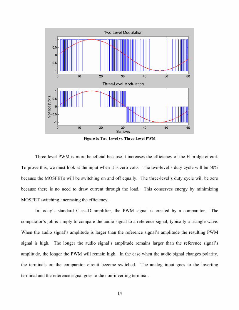
Figure 6: Two-Level vs. Three-Level PWM
Three-level PWM is more beneficial because it increases the efficiency of the H-bridge circuit.
To prove this, we must look at the input when it is zero volts. The two-level’s duty cycle will be 50%
because the MOSFETs will be switching on and off equally. The three-level’s duty cycle will be zero
because there is no need to draw current through the load. This conserves energy by minimizing
MOSFET switching, increasing the efficiency.
In today’s standard Class-D amplifier, the PWM signal is created by a comparator. The
comparator’s job is simply to compare the audio signal to a reference signal, typically a triangle wave.
When the audio signal’s amplitude is larger than the reference signal’s amplitude the resulting PWM
signal is high. The longer the audio signal’s amplitude remains larger than the reference signal’s
amplitude, the longer the PWM will remain high. In the case when the audio signal changes polarity,
the terminals on the comparator circuit become switched. The analog input goes to the inverting
terminal and the reference signal goes to the non-inverting terminal.
14
Figure 7: PWM Comparator
To achieve a proper PWM signal that will represent an analog input, the reference signal
amplitude must be larger than the maximum input amplitude. Another important factor of the reference
signal is the operating frequency or clock speed of that waveform. The operating frequency must be
faster than the audio signal to assure an accurate sampling rate.1 The faster the clock speed of the
reference signal, the closer the output will represent the input. A drawback is more Electromagnetic
Interference (EMI) will be radiated from the circuit which will be talked about later. The advantage of
an extremely high clock speed, 1MHz and up, is full audible bandwidth capabilities of the amplifier, 20
to 20 kHz. As of 2003, the Xtant 1.1i was the only Class D amplifier on the market with this capability.2
For the purposes of this project, a comparator will not be used to create a square wave signal in
the manner just discussed. A Sigma-Delta modulated signal (SDM) will be used as opposed to a PWM
signal. The SDM will be created using discrete components that accept an analog input. The analog
input will be a standard 1.4 Volt peak.
2.2.2 Sigma-Delta Modulation
To understand Sigma-Delta Modulation it is important to first understand how it originated.
Before Sigma-Delta Modulation there was delta modulation. “Delta modulation is based on quantizing
the change in the signal from sample to sample rather than the absolute value of the signal at each
sample.”3 Figure 8 shows the block diagram of the delta modulator and demodulator.
15

Figure 8: Delta Modulation and Demodulation3
Notice how the output of the integrator in the feedback loop of Figure 8(a) tries to predict the
input . This signifies that the integrator works as a predictor and the equation)(tx )()( txtx − is the
prediction error term. The prediction error term in each current prediction is quantized and is used in the
subsequent prediction. The quantized prediction error (delta modulation output) is integrated in the
receiver just as it is in the feedback loop. Finally, the predicted signal is smoothed out with a low-pass
filter and produces the channel output.3
It is important to mention that delta modulators exhibit slope-overload for rapidly rising input
signals. Slope-overload happens because the output takes a long time to catch up and follow the input.
Thus, delta modulators performance is dependent on the frequency of the input signal. On the reverse
end, granular noise can also be a problem when implanting SDM. Granular noise occurs when the step
size is too large and causes excessive quantization noise when the input changes slowly. The step size is
explained in much greater detail later in the report.
16

Integration, a linear operation, allows the two integrators in delta modulation to be combined into
one without altering the input/output characteristics. Figure 9 shows the Sigma-Delta (Σ-∆) Modulator.
Figure 9: Block Diagram of Sigma-Delta (Σ-∆) Modulation3
Sigma-Delta Modulation is a smoothed out version of delta modulation, which is why it was
chosen for this project. Both delta modulation and Sigma-Delta Modulation use a simple quantizer
(comparator) but only in Sigma-Delta Modulation does this comparator encode the integral of the signal
itself. The performance of this system is insensitive to the rate of change of the signal. Later in this
report, these noise-shaping properties will be discussed in more detail and will show why Sigma-Delta
Modulation is “well suited to signal processing applications such as digital audio and communications.”3
Sigma-Delta Modulation and Pulse-Width Modulation are similar and are applicable in the same
topologies. Both SDM and PWM quantize the signal of interest directly. The product of the encoded
waveforms when filtered can be represented in both cases by the ratio of the time the signal spends in
the high position to the time it spends in the low position over a given time. The only difference is the
time the two use to modulate the signal. The PWM signals are averaged over one switching cycle where
17

SDM are averaged over several cycles. Due to the modulation strategy for SDM, the switching
frequency is “hidden” and less harmonic energy is contained at lower frequencies.3 The frequency is
“hidden” due to the MOSFETs not switching every cycle of the clock. With PWM, switching occurs at
every instance of the reference signal. This results in a more spread out spectral density for SDM.
When comparing these two methods, the fact that SDM has a more spread out spectral density
really separates it apart from PWM. PWM uses only one switching cycle, which will have a tendency
for its power spectrum to be concentrated about the switching frequency and its harmonics, which give
rise to harmonic spikes. These spikes can produce many drawbacks for PWM with unwanted effects
such as acoustic noise, torque ripple, and electromagnetic interference. One case where the drawbacks
of SDM exceed those of PWM is at low modulation indices. With first order SDM, spectral spikes will
degrade the performance unless a dither is added. Dither will help reduce the spikes and open the door
for SDM.
2.2.3 Digital Signal Processing For this project we explored implementing a digital DSP chip as the brains of the operation. We
found that an Analog Devices chip, the ADSP-21161 SHARC® would be an excellent choice for the
signal processing. This chip is extremely versatile and meets all of our specifications. Some of these
specifications include an S/PDIF (Sony Philips Digital Interface) input, the capability of controlling the
level of accuracy needed to generate a Sigma-Delta Modulated signal, and an analog input for a
controlled feedback loop. The arrangement below shows an example of what the block diagram for the
DSP chip would look like.
18
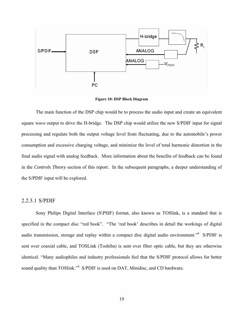
Figure 10: DSP Block Diagram
The main function of the DSP chip would be to process the audio input and create an equivalent
square wave output to drive the H-bridge. The DSP chip would utilize the new S/PDIF input for signal
processing and regulate both the output voltage level from fluctuating, due to the automobile’s power
consumption and excessive charging voltage, and minimize the level of total harmonic distortion in the
final audio signal with analog feedback. More information about the benefits of feedback can be found
in the Controls Theory section of this report. In the subsequent paragraphs, a deeper understanding of
the S/PDIF input will be explored.
2.2.3.1 S/PDIF
Sony Philips Digital Interface (S\PSIF) format, also known as TOSlink, is a standard that is
specified in the compact disc “red book”. “The ‘red book’ describes in detail the workings of digital
audio transmission, storage and replay within a compact disc digital audio environment.”4 S/PDIF is
sent over coaxial cable, and TOSLink (Toshiba) is sent over fiber optic cable, but they are otherwise
identical. “Many audiophiles and industry professionals feel that the S/PDIF protocol allows for better
sound quality than TOSlink.”4 S/PDIF is used on DAT, Minidisc, and CD hardware.
19

The S/PDIF (IEC-958) is a 'consumer' version of the AES/EBU-professional interface. Below is
table that shows the differences between S/PDIF and AES/EBU.
Table 1: AES/EBU vs. S/PDIF5
There are two distinct parts that make up an S/PDIF signal: data protocol and hardware interface.
The data protocol is universal across all S/PDIF devices. Sampling rates and resolutions between 16 and
24 bits can be supported as well as up to 4 channels. The hardware interface is what has already been
mentioned and that is how to send S/PDIF data.
The next table illustrates other important details about the Standard IEC958 "Digital audio
interface" from EBU (European Broadcasting Union).
Table 2: EBU Details Pertaining to Digital Audio Input5
20
Some key points in this table are the sampling frequencies and control information about the
inputs. These are necessary points that allow signal processing to be carried out. The signal on the
digital output of any device looks like an almost perfect sine-wave, with amplitude of 500 mVolts and a
frequency of almost 3 MHz. Each sample contains two 32-bit words that are transmitted which result in
a bit-rate of 2.8224 Mbit/s at a 44.1 kHz sampling rate for CD and DAT.5
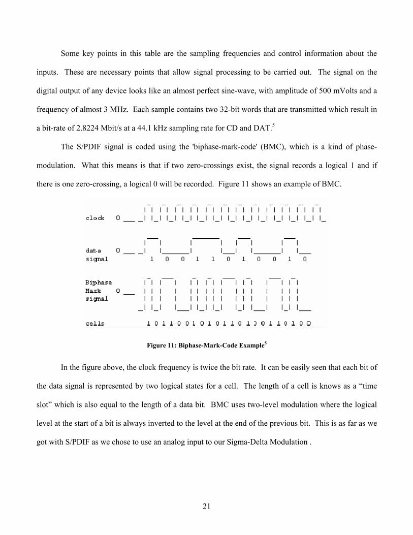
The S/PDIF signal is coded using the 'biphase-mark-code' (BMC), which is a kind of phase-
modulation. What this means is that if two zero-crossings exist, the signal records a logical 1 and if
there is one zero-crossing, a logical 0 will be recorded. Figure 11 shows an example of BMC.
Figure 11: Biphase-Mark-Code Example5
In the figure above, the clock frequency is twice the bit rate. It can be easily seen that each bit of
the data signal is represented by two logical states for a cell. The length of a cell is knows as a “time
slot” which is also equal to the length of a data bit. BMC uses two-level modulation where the logical
level at the start of a bit is always inverted to the level at the end of the previous bit. This is as far as we
got with S/PDIF as we chose to use an analog input to our Sigma-Delta Modulation .
21

2.3 PowerNet 42V Standard
In the very near future, we will see a change in the technology incorporated into all of our
automobiles. For instance, many systems that have been operated by mechanical or hydraulic power
such as brakes, valves, and steering will be replaced by electrically driven devices. As soon as 2005
some luxury cars are expected to implement these electronic devices. Other electronically driven
devices are expected to replace complex transmissions, engine power management control system
processors, infinitely variable cabin climate control systems, etc. It is clearly visible that the standard 12
Volt battery, which was adopted in the 1920s, will soon be obsolete due to its inability to support the
expected 5,000 Watts of power for the future average-sized car. Today’s cars rarely consume greater
than 1,500 Watts.
The 42 Volt system called “PowerNet” was first conceptualized in 1996 and is currently seeking
standardization. It was introduced in FAKRA (DIN Standards Committee for Road Vehicles) and VDA
(Association of German Automotive Industry) in November 1996.6 In 1997 both associations agreed
upon its standardization and are currently working out a draft acceptable by DIN and ISO. Currently the
Working Group “Standardization“(WGS) has 19 members participating including:
• FAKRA • DaimlerChrysler • BMW • VW • Hella • Varta • TÜV Automotive Süddeutschland • Infineon
• Siemens AT • AMP • Valeo • Bosch • Delphi • Sican • Renault • PSA.
The transition to a 42 Volt standard from 12 Volt is something that will occur over time.
Companies such as DaimlerChrysler and BMW are pioneering 14/42 Volt dual voltage systems. These
22

cars will have the ability to power both 14 Volt and 42 Volt components using two separate circuits.
Currently, components such as aftermarket car stereos and other mobile electronics are not ready for this
jump. As the 42 Volt system becomes more prevalent, it can be assumed that companies producing
devices such as car audio amplifiers will take advantage of this new system. One of the obvious reasons
is the greater potential that the 42 Volt system allows over the 12 Volt system.
A primary concern of the 42 Volt standard is limiting the maximum allowed voltage produced by
the automobile. In the PowerNet, the generator must supply a voltage, UPN, of 42 Volt to the vehicle’s
electrical system whereas the maximum static over-voltage is to be no more than 52 Volt including
ripple due to load dump protection (LDP) ± 5%. This is shown in Figure 12.
Figure 12: Maximum Over-voltage6
The 48 Volt effective level was determined to be the power recharging voltage of the battery.
Therefore, the peak static voltage is not to exceed 52 Volts given an 8 Volt (peak-to-peak) ripple riding
on the effective voltage level.
Perhaps the most important factors with regards to this project are the maximum and minimum
dynamic voltages. The maximum dynamic voltage for the PowerNet is determined to be 58 Volts due to
LDP. This is an important parameter when selecting semiconductors that see this unregulated power
source. Each of the MOSFETs used in this project are able to withstand this voltage since their
23
breakdown limitation is at least 60 Volts. Figure 13 shows a test waveform of the maximum overshoot
voltage.
Figure 13: Maximum Dynamic Voltage6
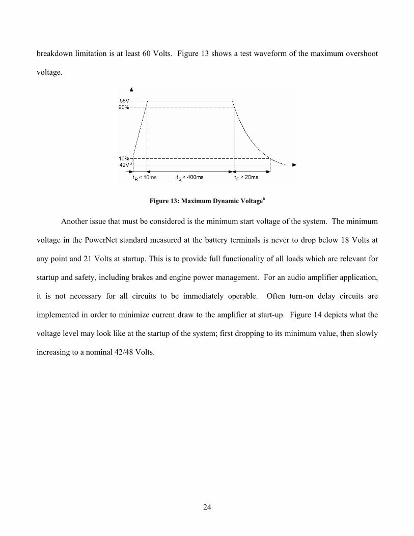
Another issue that must be considered is the minimum start voltage of the system. The minimum
voltage in the PowerNet standard measured at the battery terminals is never to drop below 18 Volts at
any point and 21 Volts at startup. This is to provide full functionality of all loads which are relevant for
startup and safety, including brakes and engine power management. For an audio amplifier application,
it is not necessary for all circuits to be immediately operable. Often turn-on delay circuits are
implemented in order to minimize current draw to the amplifier at start-up. Figure 14 depicts what the
voltage level may look like at the startup of the system; first dropping to its minimum value, then slowly
increasing to a nominal 42/48 Volts.
24

Figure 14: Starting Voltage6
Many other factors such as slow decrease and increase of the power supply voltage have also
been determined. This limitation is defined, “No undesired functions shall appear when decreasing the
operating voltage from max 42 Volts to 0 Volts and increasing it from 0 Volts to max 42 Volts.”6
2.4 Power MOSFETs It was decided to use a completely discrete set of components for the output stage for this
amplifier. The selection of the best MOSFET for this application is one of the most important steps in
achieving peak efficiency. Each chip is built with a particular purpose in mind. The job was to
determine the model that would meet or exceed the demands while remaining within the project’s
budget of $1000.
The first step in choosing output MOSFETS was figuring the appropriate breakdown voltage or
Vss. This was not difficult to calculate since it was known that the rail voltages would be +/-42 Volts
plus any additional charging voltage. Today, the automotive 12 Volt standard requires all electronics to
be able to run between the operating voltages of 8 Volts to 18 Volts. In the future, the 48 Volt
PowerNet standard will demand compliance within a 36 to 52 Volt range.6 However, since voltage
25
spikes are common with automotive alternators, a MOSFET was chosen with no less than 60 Volts for a
breakdown voltage. This helped narrow the search significantly.
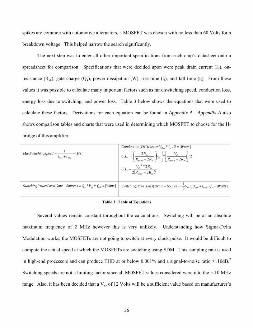
The next step was to enter all other important specifications from each chip’s datasheet onto a
spreadsheet for comparison. Specifications that were decided upon were peak drain current (Id), on-
resistance (Rds), gate charge (Qg), power dissipation (W), rise time (tr), and fall time (tf). From these
values it was possible to calculate many important factors such as max switching speed, conduction loss,
energy loss due to switching, and power loss. Table 3 below shows the equations that were used to
calculate these factors. Derivations for each equation can be found in Appendix A. Appendix A also
shows comparison tables and charts that were used in determining which MOSFET to choose for the H-
bridge of this amplifier.
][1 Hztt
ngSpeedMaxSwitchifallrise
=+
=
( )2
2
222*..
2/2
*2
2..
][2/*)(
dsLoad
dsds
dsLoad
dsds
dsLoad
ds
dRds
RRRVLC
RRVV
RRRLC
WattsIVLossDCConduction
+=
⎥⎦
⎤⎢⎣
⎡+⎥
⎦
⎤⎢⎣
⎡⎟⎟⎠
⎞⎜⎜⎝
⎛+
=
==
][**)( WattsfVQSourceGateowerLossSwitchingP clkgsg ==− ][)(21)( WattsfttIVSourceDrainowerLossSwitchingP sOFFONoin =+=−
Table 3: Table of Equations
Several values remain constant throughout the calculations. Switching will be at an absolute
maximum frequency of 2 MHz however this is very unlikely. Understanding how Sigma-Delta
Modulation works, the MOSFETs are not going to switch at every clock pulse. It would be difficult to
compute the actual speed at which the MOSFETs are switching using SDM. This sampling rate is used
in high-end processors and can produce THD at or below 0.001% and a signal-to-noise ratio >110dB.7
Switching speeds are not a limiting factor since all MOSFET values considered were into the 5-10 MHz
range. Also, it has been decided that a Vgs of 12 Volts will be a sufficient value based on manufacturer’s
26

data in order to minimize DC on-resistance, Rds. All efficiency calculations have been considered at the
predetermined load of 4Ω. Conduction loss is the largest factor in determining efficiency for the
nt through two
chips at a time we can find the total power loss in the MOSFETs by doubling this value.
operating frequency of 2 MHz.
Based on calculated results, the Fairchild FDP038AN06A0 seems to be the best MOSFET due to
its low Rds and conduction loss. As seen in Appendix A, this MOSFET dissipated a loss of 16.3
Watts/chip with an Rload of 1Ω. Since the H-bridge configuration allows flow of curre
Figure 15: H-Bridge
Therefore, the ideal efficiency limited by the output MOSFETs will be 98.14% given by the following
equation.
%14.986.17501.1718
==
=
WWEfficiency
PPEfficiency
Total
Load
Further details about efficiency calculations are given in the Efficiency section of this report.
27

2 otential Concerns
Before this project even began, there were certain issues that we thought might give us trouble in
later stages of the project. These items were filtering, and electromagnetic interference. To address
these iss
.5 P
ues, we briefly describe the types of complications we thought each might contribute to the
roject.
.5.1
filtering, the
igma-
onstruct the filter. To determine the values for the
o components, the following formulas were used:8
p
2 Filtering
In the audio industry, the audible bandwidth range is considered to be 20 – 20 kHz. Because of
this fact, all frequencies above 20 kHz will be filtered out. Filtering benefits this project in that it
reduces the signal range that the speaker would have to play. Energy is wasted in trying to play
frequencies higher than the human ear can hear and will result in a loss of energy in the form of heat.
Additionally, EMI caused from high frequencies will be kept to a minimum. Without
S Delta Modulated signal would remain digital instead of converting back to analog.
To ensure the goal of 95% efficiency, it was decided to use a passive filter. A passive filter is
able to achieve higher efficiency because it theoretically gives back all the energy that it absorbs. For
this project an inductor and capacitor will be used to c
tw
f 00*2πω =
⎟⎟⎟
⎠
⎞
⎜⎜⎜
⎝
⎛−= ⎟
⎠⎞
⎜⎝⎛
RCRC 21
2
2
021
ω
28
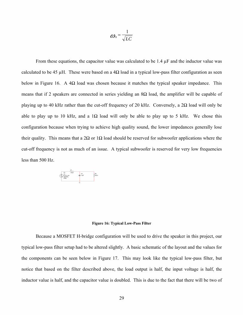
LC1
=ω
From these equations, the capacitor value was calculated to be 1.4 µF and the inductor value was
calculated to be 45 µH. These were based on a 4Ω load in a typical low-pass filter configuration as seen
below in Figure 16. A 4Ω load was chosen because it matches the typical speaker impedance. This
means that if 2 speakers are connected in series yielding an 8Ω load, the amplifier will be capable of
playing up to 40 kHz rather than the cut-off frequency of 20 kHz. Conversely, a 2Ω load will only be
able to play up to 10 kHz, and a 1Ω load will only be able to play up to 5 kHz. We chose this
configuration beca
0
use when trying to achieve high quality sound, the lower impedances generally lose
their quality. This means that a 2Ω or 1Ω load should be reserved for subwoofer applications where the
cut-off frequency is not as much of an issue. A typical subwoofer is reserved for very low frequencies
less than 500 Hz.
V31V0.71V_rms1000kHz0Deg
L3
45uHC31.4uF
R24ohm
Because a MOSFET H-bridge configuration will be used to drive the speaker in this project, our
typical low-pass filter setup had to be altered slightly. A basic schematic of the layout and the values for
the components can be seen below in Figure 17. This may look like the typical low-pass filter, but
notice th
Figure 16: Typical Low-Pass Filter
at based on the filter described above, the load output is half, the input voltage is half, the
inductor value is half, and the capacitor value is doubled. This is due to the fact that there will be two of
29

these filters in place at the H-bridge, for simplicity and ease of explanation, the model was done in this
manner.
L1
22.5uHC12.8uF
R12ohm
V10.5V0.35V_rms1000kHz0Deg
Figure 17: H-Bridge Output Low-Pass Filter
To ensure that the design will perform in the manner that it was designed, simulations were in
order.
Figure 18: Bode Plot for 1 Ohm Load
30
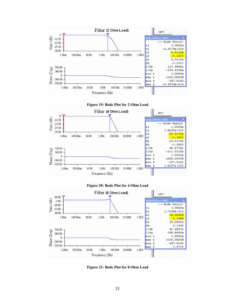
Figure 19: Bode Plot for 2 Ohm Load
Figure 20: Bode Plot for 4 Ohm Load
Figure 21: Bode Plot for 8 Ohm Load
31

erference (EMI)
rence.
EMI becomes a problem when the speaker wires from the amplifier to the speaker act like an
antennae and transmit the EMI throughout the car’s vehicle. Also, these same wires could receive EMI
that the car might transmit, interf trying to play. This is why it is
portant to keep the speaker wires as short as possible. The longer they become the better the chances
are that they will either receive or transmit EMI. Another way to keep the EMI to a minimum is to use a
braided speaker wire as shown in Figure 22. Theoretically, the EMI from one speaker wire is cancelled
out by the other one.9
The simulations show where the cut-off frequency will be for each speaker load configuration.
The calculations were very close to the simulated results with the margin of error increasing as the
impedance decreased. Notice that the last figure of the 8Ω load shows a frequency of approximately 20
kHz. This is due to the fact that there is a slight rise in the filter response before the cut-off. The rise is
approximately 3db, and that is what is shown. The actual -3dB point is in fact 40 kHz.
2.5.2 Electromagnetic Int
Electromagnetic interference is caused by rapid changes in currents. When the power stage
transitions, the switch’s output changes across the entire power supply voltage and the loudspeaker
current is re-routed through the output stage. This is the main cause of electromagnetic interference in
Class-D amplifiers. Contrary to popular belief, the voltage change is not a major issue as long as
capacitively coupled currents can be returned directly to the source using electrostatic shielding. High
changes in current value, on the other hand, will cause magnetic radiation, which is the main cause of
electromagnetic interfe
ering with the signal that the speaker is
im
32
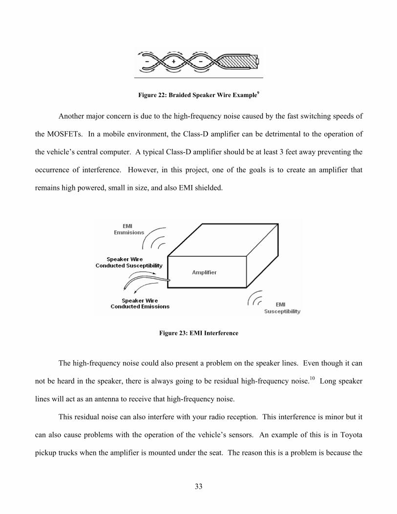
Figure 22: Braided Speaker Wire Example9
Another major concern is due to the high-frequency noise caused by the fast switching speeds of
the MOSFETs. In a mobile environment, the Class-D amplifier can be detrimental to the operation of
the vehicle’s central computer. A typical Class-D amplifier should be at least 3 feet away preventing the
occurrence of interference. However, in this project, one of the goals is to create an amplifier that
remains high powered, small in size, and also EMI shielded.
Figure 23: EMI Interference
The high-frequency noise could al
so present a problem on the speaker lines. Even though it can
not be heard in the speaker, there is always going to be residual high-frequency noise.10 Long speaker
This residual noise can also interfere with your radio recep n. This interference is minor but it
can also cause problems with the operation of the vehicle’s sensors. An example of this is in Toyota
is because the
lines will act as an antenna to receive that high-frequency noise.
tio
pickup trucks when the amplifier is mounted under the seat. The reason this is a problem
33

vehicle
he braided material is wrapped around several of the components such as the MOSFETs,
the hea
a mobile environment. Another
material to look at is steel. Steel is a compromise between both shielding and heat transfer but adds
weig es not fully s all frequencies and still do heat as well as
alum
’s central computer is also located there. This poses a problem because if the EMI affects the
computer of the vehicle, it will affect the vehicles performance, and could create a safety concern. Also,
the high-frequency noise carried through the line will be absorbed by the voice coil of the speaker. This
noise is extra energy that the voice coil absorbs, causing it to not only heat up, but also waste energy in
the process.
To face these problems, EMI shielding must be implemented into the design of the amplifier.
Currently, there is no shielding in Class-D amplifiers. The manufacturers warn consumers that the
amplifier must be at least 3 feet from the car’s central computer.10 In this project, the amplifier will be
designed so that the user may place it wherever it is convenient without worrying about where the
central computer is located. To do this, three methods have been considered.
The first is a braided material that can be purchased that shields EMI very effectively. The trade-
off is that if t
t transfer from the component to the heat-sink would be compromised due to the nylon casing
that surrounds the sheilding. This could solve the EMI problem without adding excessive cost to the
amplifier, but lacks the thermal capabilities of heat dissipation to the heat sink.
The second possibility is to design both a base and heat sink for the amplifier that is naturally
EMI shielded. One example would be lead, which is great at shielding, but not as great at dissipating the
heat like aluminum.11 Also, implementing lead as a heat sink and an effective EMI shield would greatly
increase the weight of the entire amp which would not be good in
ht and do hield against es not dissipate
inum.12
34

A third method is to sti at sink, but if
we used perforated aluminum we can h shielding and heat-sink. Tests have
roven
effectiveness of 92dB provides 99.997% effectiveness.13 Our amplifier will meet or exceed the FCC
in uncertain at this time. The perforated aluminum appears to be the most effective way to go, but the
cost of implementing perforated aluminum has yet to be determined.
Shielding Possibilities
use perforated metals. Aluminum can ll be used as the he
serve the purpose of bot
p that a shielding effectiveness of 40dB provides 99.000% attenuation of EMI, and that a shielding
regulation of 100 µVolts/m at a distance of 3 meters; however the attenuation required for the amplifier
Material Advantage Dis-Advantage 1. In-expensive 1. Difficult to work with. Shielded Braiding
Material 2. Lacks heat transfer properties 1. Serves as both shielding and heat-sink 1. Very heavy
Naturally Shielded Heat 2. Most metals either good at Sink
shielding or heat sink, not both.
1. Serves as both shielding and heat-sink 1. Thicker heat-sink Perforated Aluminum 2. Lightweight 2. Slightly more expensive
Table 4: Shield Possibilities
Active research continues on reducing interference by inspecting new arrangements for
components to either reduce or completely eliminate the electromagnetic waves. This is certainly an
area that must be fully explored but will be much easier once the design of the amplifier is complete.
2.6 Efficiency
The most limiting factor in achieving high-efficiency is in the final stage of any amplifier. The
theoretical efficiency of a Class-D amplifier is 100%, but unfortunately it is also limited by non-ideal
components. In addition, the increasing switching speed necessary to produce a clean audio output also
35

reduces this factor by a great deal. This section will attempt to describe the effects of discrete MOSFET
shortcomings.
In our amplifier, we chose to use a standard MOSFET H-bridge power stage. This allows us to
apply both a positive and negative voltage to the load somewhat easily. Another alternative commonly
used in an amplifier output stage is the push-pull BJT pair found in Class-AB amplifiers where the
output stage consists of an NPN and a PNP transistor. As the input sweeps from VEE to VCC, the output
passes through a dead zone of 1.4 Volts in which both transistors are off. This dead zone causes
rossover distortion which can be avoided when using MOSFETS and either a Sigma-Delta or Pulse-
idth
c
W modulated signal. Figure 24 below shows a basic model of our circuit.
Figure 24: Basic level circuit model
In Figure 24 there are four N-MOS devices. In an H-bridge configuration as the one depicted
below, current may take one of two paths.
36

Figure 25: Current paths through the H-bridge
Sigma-Delta technology implies that the signal be switched from 0 Volts to either rail voltage
rapidly enough to represent an analog signal. This means that for any given pulse, the output must
change 42 Volts. The fact that MOSFETS are not ideal and contain capacitive and inductive properties
limits the speed at which this switching occurs. In order to simulate the effects of such characteristics
one would need to simulate the complex model of each MOSFET in a circuit. We have circumvented
such testing due to time limitations and have found equations to give linear approximations of the
output. These can be found further along in this section.
There are in fact two sources of loss from switching a MOSFET. The first is due to changing the
drain to source voltage limited by Cds and the second from changing the gate to source voltage by Cgs.
For our purposes, a linear approximation of the power loss due to switching from both the drain to
source and gate to source will suffice. Figure 26 gives an accurate representation of what we are trying
to calculate.14
37

Figure 26: MOSFET Switching Losses
The new simplified equation uses common specifications given by manufacturers and therefore
may be estimated before purchasing any of the MOSFETs. The equations used to find the power loss
are listed in Table 5 and are explained in the Appendix.
][**)( WattsfVQSourceGateowerLossSwitchingP clkgsg ==− ][)(2
)( WattsfttIVSourceDrainowerLossSwitchingP sOFFONoin =+=−1
( )222..
2/2
*2
..
][2/*)(
dsLoad
dsds
dsLoadds
dsLoad
dRds
RRLC
RRV
RRLC
WattsIVLossDCConduction
+=
⎥⎦
⎢⎣ +⎥
⎦⎢⎣
⎟⎟⎠
⎜⎜⎝ +
=
==
2 2*
2 dsds
RV
VR ⎤⎡⎤⎡ ⎞⎛
dsloadds
rail
DCsgswsdsw
loss
RRR
PPPEfficiency
PEfficiency
**2
)(2*100100
2*100100
2,,
⎟⎟⎠
⎜⎜⎝ +
++−=
−=
−−
V
Ptotal
⎞⎛
Table 5: Power Loss and Efficiency Equations
From the calculations in the Power MOSFET section of this report, one can see that the
efficiency of the Fairchild FDP038AN06A0 is adequate enough for us to achieve our goal of 95%
et or exceeded 95% efficiency at our test frequency of 192 kHz,
this mo
not
efficiency. While other MOSFETs m
del was the most efficient. This has been made possible by a small Rds value and reasonably
small Qg value. These two specifications are the most significant in gaining efficiency.
As Rds or Qg increase, efficiency decreases proportionally. These specifications are also
inversely related which means that a When manufacturing a MOSFET a design consideration has to be
made because it is not possible to decrease both Rds and Qg at the same time. Currently it is
38

possible to decrease both factors at the same time. Perhaps a different fabrication process will some day
minimize these limiting factors. However, since Rds is a much larger factor to consider, we chose the
MOSFET with the least DC-on resistance.
Semiconductor technology continues to advance every year. New ways of making faster, higher-
power, and smaller devices are being discovered all the time.15 These minimize both the size and cost of
the electronic devices. Next year there will be an even better selection of MOSFETs to implement and
raise efficiency once again. The most important factors to look for when deciding on any switching
device would be its DC-on resistance, u re in excess of 10 MHz. The advent of
lity. If employed correctly, it may safeguard the overall output of the amplifier from variations in
the rail
nless switching speeds a
these new components shall push the limits of efficiency and give engineers the tools they need to make
amplifiers switch faster and ultimately produce higher fidelity sound.
2.7 Controls Theory
A certain level of control must be implemented in the system to protect against the frequent
instability of an automobile environment. Feedback is a common method for dealing with this
instabi
voltages and unwanted energy produced by the signal processing. A simple block diagram of the
system gives a better understanding of how the output can be used to correct these simple problems.
39

Sigma DeltaModulation
AnalogInput H-Bridge Low Pass
Filter
Feedback
Figure 27: Block Diagram
ent, the output will remain high
the output should not deviate from the input apart from the
ain.
t voltage as a midpoint, relative voltage swings can be
duty cycle of the Sigma-Delta modulated signal. For instance, if the
average voltage of a PowerNet system is 48 Volts and voltage drops to 44 Volts, the duty cycle must
increase by 8.33%.
A main concern of this MQP is to maintain a certain level of total harmonic distortion (THD).
Since the rail voltage of the H-bridge is entirely dependent on the automobile’s PowerNet voltage, a
wide range of values must be tolerated without alteration to the speaker output. This means that if a
lower voltage is present, then the output may need to remain “high” for a longer period of time to reach
an equivalent analog value. Conversely, if a higher rail voltage is pres
for a shorter period of time. If done properly,
g
Figure 28 shows that as the rail voltage changes, the duty cycle must be changed to achieve a
steady output. By using the average outpu
calculated and used to modify the
%33.848
4448=
−=
−=
i
if
VVV
DutyCycle Conversely, the duty cycle must be
decreased by 8.33% if rail voltage rises to 52 Volts.
40
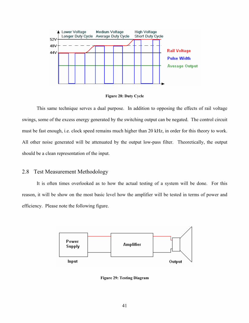
Figure 28: Duty Cycle
order for this theory to work.
All other noise generated will be attenuated by the output low-pass filter. Theoretically, the output
should be a clean representation of the input.
ing of a system will be done. For this
reason, it will be show on the most basic level how the amplifier will be tested in terms of power and
efficiency. Please note the following figure.
This same technique serves a dual purpose. In addition to opposing the effects of rail voltage
swings, some of the excess energy generated by the switching output can be negated. The control circuit
must be fast enough, i.e. clock speed remains much higher than 20 kHz, in
2.8 Test Measurement Methodology
It is often times overlooked as to how the actual test
Figure 29: Testing Diagram
41

By measuring both the voltage and current at the power supply, the input power of the amplifier
can be determined using the following formula:
VIPIN ∗=
By finding the RMS voltage out of the amplifier, the output power of the amplifier can be
etermined using the following formula: d
RV 2
POUT =
From the actual power of the amplifier, the efficiency can be calculated. The theoretical
efficiency has already been determined in the MOSFET section of this paper. If the measured output is
divided by the input power, this will yield the efficiency of the amplifier.
EfficiencyInputPower
rOutputPowe=
If a 1Ω load was used for testing in lab, the testing equipment would have to be capable of
handling 42 Amps of current. Such equipment is expensive, and might not be readily available.
However, we will not be testing at such a low load impedance.
42
3 Design The design of a Class-D car audio amplifier is a complex and faceted undertaking. The design
stage of any project requires the most time and effort, and is also the most crucial to success. The design
considerations we took into account for this project were signal processing, power output and
amplification, filtering, thermal relief, and printed circuit board layout.
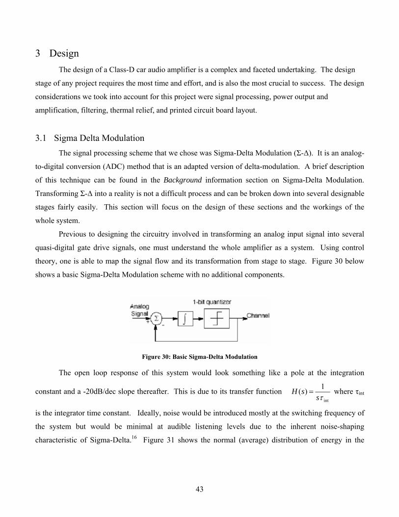
3.1 Sigma Delta Modulation The signal processing scheme that we chose was Sigma-Delta Modulation (Σ-∆). It is an analog-
to-digital conversion (ADC) method that is an adapted version of delta-modulation. A brief description
of this technique can be found in the section on Sigma-Delta Modulation.
ents.
Background information
Transforming Σ-∆ into a reality is not a difficult process and can be broken down into several designable
stages fairly easily. This section will focus on the design of these sections and the workings of the
whole system.
Previous to designing the circuitry involved in transforming an analog input signal into several
quasi-digital gate drive signals, one must understand the whole amplifier as a system. Using control
theory, one is able to map the signal flow and its transformation from stage to stage. Figure 30 below
shows a basic Sigma-Delta Modulation scheme with no additional compon
Figure 30: Basic Sigma-Delta Modulation
The open loop response of this system would look something like a pole at the integration
constant and a -20dB/dec slope thereafter. This is due to its transfer function int
1)(τs
sH = where τint
is the integrator time constant. Ideally, noise would be introduced mostly at the switching frequency of
the system but would be minimal at audible listening levels due to the inherent noise-shaping
characteristic of Sigma-Delta. distribution of energy in the 16 Figure 31 shows the normal (average)
43

h ics of this noise. One can see the decline in magnitude within the audible band. All higher
frequency noise is filtered out using a low-pass filter as described in the Filter section of this report.
armon
Figure 31: Noise Spectrum
In the design of our amplifier, we chose to modify the basic modulation scheme depicted in
in our H-bridge
onfiguration separately. This control over all the MOSFETs simultaneously was crucial in creating a
three-level output signal. The functionality of how the MOSFETs create these three states can be found
in further detail in the Power Stage section of this report. This additional control would minimize power
loss from drain to source switching, given the following equation:
Figure 30. By adding a second 1-bit quantizer, or comparator, we were able to generate four separate
gate signals to drive the four n-channel enhancement mode MOSFET devices
c
][)(21 WattsfttIVP sOFFONoinDS =+=−
.17
Discussion of this topic can be found in the Efficiency section of the report. This more advanced Sigma-
Delta Modulation scheme is shown in Figure 32.
Figure 32: Three-Level Sigma-Delta Modulation
44

The signal path can be described using Figure 32 above as a visual aide. First, (1), the signal
arrives at the amplifier from the audio source as an analog waveform of either music or a test tone.
Since S
rms. This
keep track of this error, continuous integration takes place resulting in a “sum of errors” waveform at
them in such anner to switch the four MOSFET devices. At location 5, the signal is very much still
digital but greatly amplified to the level of +/- the rail voltage. After the amplified signal is filtered
igma-Delta Modulation requires a feedback loop in order to take the difference from input versus
output, signal 7 is best described as a scaled down version of the output. Signal 2 is therefore the
difference between the input and output wavefo may also be called the “error.” In order to
signal 3. Using two 1-bit quantizers, four quasi-digital streams, signal 4, are generated to control the
gates of the H-bridge. The power stage of the amplifier receives these streams and is able to interpret
a m
using a 2-pole Butterworth filter, the result is signal 6, an amplified version of the original analog signal.
This loop is continued indefinitely.
Now that the system has been described, each module involved can be delineated separately.
Starting with the integrator, the schematic in Figure 33 shows the basic configuration.
Figure 33: Integrator
The integrator portion of the signal processing loop shown above has three important tasks. The
first is to take the difference between input and feedback. This is shown in the blue square marked Delta
including a pair of resistors whose center is the output. Since the input and output are roughly the same
but opposite in sign, one can expect this waveform to fluctuate closely around zero volts. While testing,
we did not capture this waveform since the magnitude was essentially zero. The second task is to
45

compute the integral of the signal at its negative input terminal. The final duty required for the
integrator to accomplish is the addition of a zero as illustrated in the next paragraph.
As described in the Stability section of this report, it is necessary to implement both a pole and
zero into the integration of the signal to achieve stability. The zero of the integrator was determined to
be 20 kHz using a Miller integrator equation of CR
fz
z π21
=
the resistor v
. The pole of the integrator was determined
by using the same equation, however this time alue used to determine the pole was taken
from the negative feedback of the integrator. This yielded a pole at 7 kHz using the equation
CRf
pp π2
1= .18
The next stage of Sigma-Delta Modulation was to implement comparators as high and low 1-bit
quantizers. This was actually performed by using two comparators whose negative inputs saw either a
voltage slightly higher or lower than zero. This voltage margin was called the “dead-zone” voltage due
to the fact that any output of the integrato is level resulted in zero switching of the
finely tune this margin using a plug-and-check method. The resistor value that yielded the least
r between zero and th
output. We found that the calculation of such a value is a trivial matter since, in testing, it was best to
crossover distortion and optimal switching efficiency was 620Ω. Using this ratio of resistors, the
corresponding voltage for the dead-zone was computed to be mVk
VVDZ 90620100
620*15 =Ω+Ω
Ω= . The
need and application of a resistor divider network to accomplish this voltag
e margin can be read about in
e Dead-Zone section of this report. As the sum of errors was compared to these near zero voltages,
TTL logic level voltages are sent to a D-latch flip-flop which converts the two outputs to four quasi-
digital streams: ,
th
1Q 1Q , 2Q , and 2Q . Figure 34 shows the resistive voltage divider, comparators, and
flip-flop.
46

Figure 34: Quantizers
If and the 1Q 2Q waveforms are plotted on the same axis, this gives the illusion of three-level
a-Delta switching. While this waveform does not directly exist, the output of the H-bridge does
follow the switching pattern seen in Figure 35. To further clarify, what appears to be switching either
or negativ
Sigm
positive e is really a change in polarity at the load. However this three-level state is what the
load thinks it is seeing, which is why we say that it does not directly exist.
Figure 35: Three-Level Switching
47

Since the H-Bridge is described in a different section of this report, we can jump to the final
division of designing the signal processing segment of the amplifier. The feedback attenuation block is
simply an instrumentation amplifier, or In-amp, that has been calibrated to the specific gain of our
amplifier.
Figure 36: Feedback Attenuation
We were able to determine the values of these resistors by using the low frequency gain of the
system, 2R
A −= .19 In our case, the amplification factor of the amplifier is about 30, so R2 must be 30
times greater than R1. This com
1R
pletes the Sigma-Delta Modulation signal processing piece of our report
. Because the signal is three-level, there are 3 possible
and is now important to discuss the power output and final stage of the amplifier.
3.2 Power Stage After the input signal passes through our Sigma-Delta Modulation scheme, we then devised a
way to control the MOSFETs of the H-Bridge
output configurations that the MOSFETs must be in. Figure 37 shows the three possible MOSFET
configurations.
48

Figure 37: Three possible MOSFET configurations
In order to achieve the three states shown above, we had to use all the resources available to us.
This meant that we had to use all four outputs of the flip-flop to control the MOSFETs individually. To
accomplish this goal, we used the output of the 1Q pin from the flip-flop to control the A-side High
MOSFET (BH) to be turned on. The way the flip-flop is configured, this corresponds to the
MOSFET, otherwise known as AH. This means that if the logic output sees a high, it triggers this
MOSFET on. On the flip side, if the logic output sees a negative high, then we want the B-Side High
2Q pin.
e to achieve this, the AL
These two states are what control the majority of the switching; however there are still two more
connections to be made.
When the AH MOSFET is on, the AL MOSFET must be off. In ord r
1MOSFET was connected to the Q output pin of the flip-flop. This ensures that the AH MOSFET and
the AL MOSFET will never be both on or off at the same time. The same type of configuration occurs
on the B-Side. When the BH MOSFET is on, the BL MOSFET must be off to prevent a short to ground
as well. This means the BL MOSFET must be connected to the 2Q output pin of the flip-flop to ensure
it is always opposite from the BH MOSFET.
This leads us into a discussion of the final configuration of the MOSFETs, which we will call the
zero state. For the time duration when neither the AH or the BH MOSFETs are on, we need a third
state, zero. During this time, we turn both the AL and the BL MOSFETs on, grounding both sides of the
speaker. Having this third state is what allows us to maximize efficiency because we are not wasting
energy when not needed.
49
The output from our Sigma-Delta Modulation is what tells the MOSFETs when to turn off and
on, but there is one other device that was not yet mentioned. Between the flip-flop and the MOSFETs is
would be under normal operating
conditi
Transfer functions are equations that help relate both gain and phase shift to a circuit. A typical
transfer function has the form
a driver chip. A driver chip was chosen for two reasons. The first reason is because it has built in logic
protection to ensure that 42 Volts is never shorted to ground. The second reason is because the driver
chip we chose can source up to 1 Amp of current per gate drive. What this means is that it will turn each
of the MOSFETs off and on with more power, resulting in quicker turn-on and turn-off times. The
actual schematic of the Power Stage can be found in the Appendix.
3.3 System Stability A major concern in designing our amplifier was how stable it
ons. A circuit must be able to operate without unwanted resonance that may be damaging to its
components. Each part of the amplifier was tackled by finding their individual transfer functions to
avoid unwanted resonance. This section of the report discusses the different parts of the amplifier and
how they each help or hurt the stability of the system.
)()()(
sPsZsH = . The two polynomials, Z(s) and P(s), allow the zeros and
poles of the system to be found. Zeros are values for s that make Z(s) = 0 and the overall gain of the
system zero. Poles are values that make P(s) = 0 and the overall gain infinite20. In addition, a zero
produces a phase-shift of +90° while a pole produces a phase-shift of -90°. 21
The low pass filter used in the power output stage of the amplifier plays a large role in
aintai
initely, causing the system to crash.
Now, instead of the negative feedback being able to correct for any imperfection in the output as
described in the Sigma-Delta section of the report, the noise is reinforced. It is preferable to have a
phase at which gain is 0dB of 145°or less.22 This is also called the phase margin, or difference between
m ning stability. This filter is 2nd order, which means it has two cutoff frequencies. These
frequencies are calculated in the Filter section of this report to be at 14 kHz and 40 kHz. Together these
two poles (low-pass cutoffs) add an additional -90° of phase shift to frequencies above each of their
cutoffs. If the open-loop gain at these frequencies approaching -180° phase shift is not less than 1, or
0dB, resonance may become a problem. This could be detrimental to any system taking negative
feedback from the output because the resonance could oscillate indef
50

0dB phase and -180°. Later in this section it is shown that a phase margin of 35° is required for
stability.
The other source of poles and zeros comes from the Miller integrator used in Sigma-Delta
processing. It was determined that our system could not tolerate any more poles without zeros, therefore
an additional resistor was added in series with the capacitor of the integrator. Please reference the
Sigma-Delta section of this report for this schematic and cutoff frequency calculation. The pole of the
integrator was located at 7 kHz while the zero was introduced at 20 kHz. The location of the zero was
chosen purposely close to the 14 kHz pole of the output low-pass filter. This zero would offset the
phase shift and decrease the attenuation [in dB per decade] caused by the pole. The result of this action
is such that neither pole nor zero h
The cancellation of pole and zero then allowed us to determine the frequency at which to make
ulation was not a
mple one to make. Therefore a graphical method was used to determine this value. First, we had to
determine the DC gain of our system. Using the equation below, it was computed to be the following:
ave an overall effect on the system.
our integration pole while maintaining a phase margin greater than 35°. This calc
si
⎟⎟⎠
⎞⎜⎜⎝
⎛=
IN
OUT
VVA log20
⎟⎠⎞
⎜⎝⎛=
VVA
642log20
dBA 16=
We then decided to draw a Bode Plot of our system. The DC gain of our amplifier is 16dB and
therefore can be regarded at the starting point of our Bode Plot. Figure 38 helps illustrate the graphical
method we used in obtaining the integrator pole. By reducing the frequency of this pole location, the
magnitude curve is shifted down and phase margin decreased. Conversely, increasing the frequency of
the integrator pole shifts the magnitude cu argin increased. The value at which the
sulting phase margin is 35° is 7 kHz and can be seen in Figure 38.
rve up and phase m
re
51

Figure 38: Graphical Bode Plot Method
The final bode plot of the system can then be plotted. This can be seen in Figure 39.
Figure 39: Bode Plot
From Figure 39 one can see that the system is stable. This is justified by the phase margin of
about 35°. In this amplifier, the output filter relies on a 4Ω load for stability. If the gain of the amplifier
was increased or load changed to different impedance, the system may become unstable.
52

3. ilter One of the most critical stages of our amplifier was our filter. Without it, a sinusoidal input
would remain in the form of a three-level Sigma-Delta Modulated output. This signal would contain a
great deal of unwanted high frequency content. This energy at frequencies up to the fastest resp
4 F
onse
frequency of the driver chip may be potentially dam ging to a speaker and would use any speaker wire
as an antenna for radiating EMI. In order to solve this problem, a low-pass filter was introduced to the
circuit to cutoff any frequencies higher than approximately 20 kHz. This is because the human ear can
only hear from 20-20 kHz, so any frequencies higher than this would result in wasted energy that the
y
e Stability section
of this report.
Separating the poles of the filter turned out to be a much more difficult task than anticipated.
Early in the project, we knew that inductors would have to be ordered. Originally, we thought that we
would be able to run a 1Ω load, resulting in nearly 50 Amps of current to be drawn through the
inductors. Because of the high current rating of the inductors required for our specifications, the
inductors had to be custom made. This resulted in a fairly costly investment for our amplifier, so once
we had the inductors in our possession, we could not afford to send away for new ones. This posed a bit
of a problem for our design. In order to determine the cut-off frequencies for our filter, the two
equations below were used.
a
speaker would try to play.
Originally, we thought we could create a second order Butterworth filter with a double pole at 20
kHz. However, the filter got slightl more complicated when we introduced our Sigma-Delta circuit.
The problem that arose was that we then had to be concerned with the stability of our system. The
details on the stability of our system can be found in the Stability section of this report. From a design
standpoint the only thing we needed to know was that the poles had to be separated, meaning that there
could not be a double pole at 20 kHz. Again, the reasoning for this can be found in th
1
LRf
CL
∗=
∗
π
π
2
2
2
f =1
53
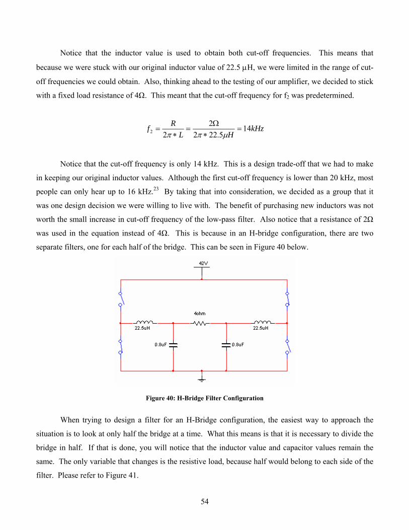
Notice that the inductor value is used to obtain both cut-off frequencies. This means that
because we were stuck with our original inductor value of 22.5 µH, we were limited in the range of cut-
off frequencies we could obtain. Also, thinking ahead to the testing of our amplifier, we decided to stick
with a fixed load resistance of 4Ω. This meant that the cut-off frequency for f2 was predetermined.
kHzHL
Rf 145.222
222 =
∗Ω
=∗
=µππ
Notice that the cut-off frequency is only 14 kHz. This is a design trade-off that we had to make
in keeping our original inductor values. Although the first cut-off frequency is lower than 20 kHz, most
people can only hear up to 16 we decided as a group that it
as one design decision we were willing to live with. The benefit of purchasing new inductors was not
40 below.
kHz.23 By taking that into consideration,
w
worth the small increase in cut-off frequency of the low-pass filter. Also notice that a resistance of 2Ω
was used in the equation instead of 4Ω. This is because in an H-bridge configuration, there are two
separate filters, one for each half of the bridge. This can be seen in Figure
Figure 40: H-Bridge Filter Configuration
When trying to design a filter for an H-Bridge configuration, the easiest way to approach the
e. What this means is that it is necessary to divide the
situation is to look at only half the bridge at a tim
bridge in half. If that is done, you will notice that the inductor value and capacitor values remain the
same. The only variable that changes is the resistive load, because half would belong to each side of the
filter. Please refer to Figure 41.
54

Figure 41: H-Bridge Filter Half Representation
The circuitry remains exactly the same, and you will notice that there is still a 4Ω load in place.
However, when looking at the filter half representation, only 2Ω belongs to each filter, which is the
reasoning behind the 2Ω being used in the f2 equation rather than the 4Ω.
After we accepted the first cut-off frequency to be 14 kHz, it was then time to set the second cut-
flexibility to change the capacitor val ce again we already had purchased several 0.1 µF
capacitors, so we decided to use those as well. This was not as big of a concern be
off frequency. Notice that the inductor value is also included in this equation, but we do have the
ue. On
cause we had the
ability to add as many 0.1 µF as we wanted, giving us a range of overall capacitance. Knowing that our
first cut-off frequency was 14 kHz, we decided to make the second cut-off frequency approximately 40
kHz. This would be well past the audible range, but still low enough in frequency to reduce EMI.
Using the formula for f1, we were able to compute what capacitor value was desirable to yield a cut-off
frequency of 40 kHz.
FCCH
kHzCL
f µµππ
7.05.222140
21
1 =→∗
=→∗
=
Based on this formula, the capacitance value that should be used is 0.7 µF. This would be easy
to obtain from the 0.1 µF capacitors that we already had by configuring 7 of them in parallel. Figure 42
shows how the filter may look from a schematic perspective.
55

Figure 42: H-Bridge Filter Design Configuration
One of the reasons that w in parallel rather than one big
apacitor was to reduce the equivalent series resistance, or ESR of the capacitors. The ESR is a
lcula
e decided to use multiple capacitors
c
ca ted resistance at a particular frequency. As the frequency increases, the ESR decreases linearly.
This was an important factor to take into consideration because at low frequencies, the ESR is relatively
high, measuring at 1.6Ω for the capacitors we chose. However, AC current through this series resistance
would be lower at low frequency since dtdvCI = . A high ESR would be detrimental to our efficiency,
and will be talked about in further detail in the Efficiency Losses section of this report.
Although the configuration shown in Figure 42 would have worked, this was not the layout that
we chose for our filter. If you count the total number of capacitors in the circuit, you will find that 14
capacitors would be necessary in order to produce our filter. There is a way to reduce the total number
of capacitors used that create the same filtering effects. The way to achieve that is to use some of the
apacitors across the load instead. Please refer to Figure 43 for further clarification. c
56
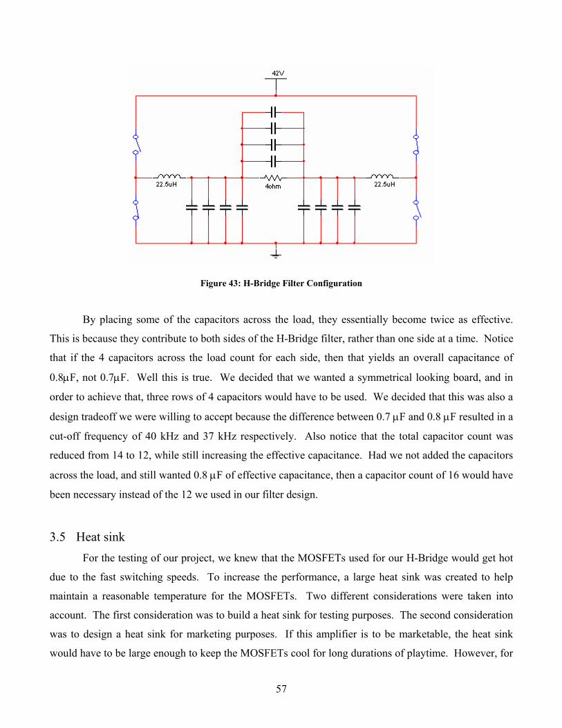
Figure 43: H-Bridge Filter Configuration
By placing some of the capacitors across the load, they essentially become twice as effective.
This is because they contribute to both sides of the H-Bridge filter, rather than one side at a time. Notice
that if the 4 capacitors across the load count for each side, then that yields an overall capacitance of
0.8µF, not 0.7µF. Well this is true. We decided that we wanted a symmetrical looking board, and in
order to achieve that, three rows of 4 capacitors would have to be used. We decided that this was also a
design tradeoff we were willing to accept because the difference between 0.7 µF and 0.8 µF resulted in a
cut-off frequency of 40 kHz and 37 kHz respectively. Also notice that the total capacitor count was
reduced from 14 to 12, while still increasing the effective capacitance. Had we not added the capacitors
across the load, and still wanted 0.8 µF of effective capacitance, then a capacitor count of 16 would have
been necessary instead of the 12 we used in our filter design.
3.5 Heat sink For the testing of our project, we knew that the MOSFETs used for our H-Bridge would get hot
due to the fast switching speeds. To increase the p ance, a large heat sink was created to help
aintai
erform
m n a reasonable temperature for the MOSFETs. Two different considerations were taken into
account. The first consideration was to build a heat sink for testing purposes. The second consideration
was to design a heat sink for marketing purposes. If this amplifier is to be marketable, the heat sink
would have to be large enough to keep the MOSFETs cool for long durations of playtime. However, for
57

the testing of our amplifier in lab, we decided that 15 minutes of playing time would be more than
sufficient to test the amplifier and obtain our results. It was decided to construct an adequate heat sink
for our purposes of testing in lab, and to design another that would be used as both a housing and a heat
sink if the amplifier was put into production.
For testing purposes, two heat sinks were fabricated out of a solid piece of aluminum. The
aluminum was donated to us by A & R Plastics Inc. as well as their machine shop for fabrication of our
ensions of 2.25”x 2”x 1.375”. An actual picture of the heat sink used for testing can be seen
Figure 44 below.
heat sinks. The design of the heat sinks presented some constraints. One constraint was how wide the
heat sinks could be by the amount of space we had on our board between components. Our second
constraint was the depth of the heat sink, which was limited by the depth of our board.
We chose aluminum for the design of our heat sink because of its light weight and thermal
properties. Secondly, in order to maximize the surface area of the heat sink to the ambient air, cooling
fins were added to the design. Generally the more cooling fins that a heat sink has, the better job it will
do at keeping the components cool. The heat sink was made larger than necessary, but in our situation it
was best to over estimate the need for thermal protection. This yielded two identical heat sinks with
overall dim
in
Figure 44: Heat sink used for testing
Figure 45: Heat sink shown with supports
One of the problems that we encountered with such a large heat sink was the weight of the
finished product. The heat sink could have been made smaller, but since the product was already
finished, we thought it would be best to leave it alone. Because we had a machine shop at our disposal,
we decided to drill and tap some supports into the fins of the heat sink. This would allow us to use
58

Teflon screws to support the weight of the excessively large heat sink. After it was mounted to the
board, the idea worked out quite well. Figure 45 shows a heat sink mounted to the MOSFETs with
supports in place to help reduce the load the MOSFETs would have to carry. Although it may not look
as professional as it should, the idea worked, and so did the heat sinks. We were able to play music,
which causes the most amount of switching, for approximately 15 minutes before the heat sinks started
to get too hot. We were able to conduct all of our testing with the heat sinks shown.
In the event that our amplifier is to be sold in today’s market, the amplifier would have to be
contained in a solid casing of some sort. This means that the heat sinks can not be two large objects
attached to the MOSFETs. Instead, the MOSFETs would be placed at the very edge of the board, and
the casing surrounding the am ould be incorporated into the
esign for what would hopefully be fan cooled. In addition to this casing being used as both a heat sink
ore all
thers. This was the case in the design of our PCB as well. In particular, high-power switching
MOSFET devices were a major concern and had to be dealt with carefully. We knew that under the
high current and fast switching they would be subjected to, heat was an issue. In order to deal with the
thermal protection of the MOSFET devices, large heat sinks would be required. Through our experience
with other audio amplifiers we were able to determine their best location. By aligning the TO-220
packages along the edges of the PCB and facing heat sink tabs outward, we would be able to effectively
build as large of a heat sink as necessary. All other devices were not as much of a concern in this stage
of PCB design.
plifier would double as a heat sink. Fins w
d
and an outer housing unit, it would also serve as an EMI shield which was discussed in the Background
section of this report. The actual fabrication of this type of device was not made, however it is
important to point out the need for a housing in the event of a continuing MQP or for marketing
purposes.
3.6 Printed Circuit Board The design and layout of any printed circuit board is a very cognitive task. One must first
analyze the components that will ultimately populate the board and their needs. Secondly, the basic
shape of the board can be determined. Thirdly, any components including input and output terminals
requiring special locations can be placed. Lastly, the remainder of parts can be laid out using good
engineering practices described in this section.
Often times certain components require special locations and must be considered bef
o
59

Figure 46: Placement of MOSFETs for Heat Sink
Determining the fundamental shape of our board was one of the more elementary steps in laying
out our design. While many basic and industry standard
ape is still the rectangle. Since our design followed a strict flow of information in one direction, an
forms and sizes may have worked, the most
sh
elongated rectangle certainly seemed the most reasonable model. This would allow for as much surface
area as required by heat sinks as well as minimizing wasted space.
The layout of the final board design was the next step to take place. As mentioned previously,
the flow of our signal path was strictly unidirectional if feedback were ignored. Therefore we found it
best to divide the PCB into sections, much like our circuit for both simplicity and practicality. One side
of the board was clearly designated as the signal processing portion whereas the other was reserved for
the power output section. These two divisions are distinct from one another in their requirements so
were best left separate. On one hand, the signal-processing side is filled with mixed signals and high-
transient voltage transmission lines. Adversely, the power output stage of the amplifier requires large
ground planes, many wide current paths, and spacing between thermally dangerous components.
60
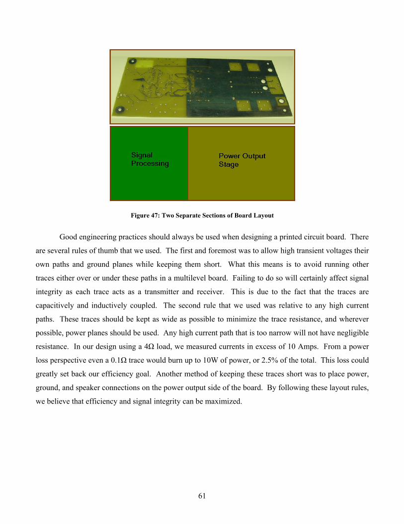
Figure 47: Two Separate Sections of Board Layout
Good engineering practices should always be used when designing a printed circuit board. There
are several rules of thumb that we used. The first and foremost was to allow high transient voltages their
own paths and ground planes while keeping them short. What this means is to avoid running other
traces either over or under these paths in a multilevel board. Failing to do so will certainly affect signal
tegritin y as each trace acts as a transmitter and receiver. This is due to the fact that the traces are
capacitively and inductively coupled. The second rule that we used was relative to any high current
paths. These traces should be kept as wide as possible to minimize the trace resistance, and wherever
possible, power planes should be used. Any high current path that is too narrow will not have negligible
resistance. In our design using a 4Ω load, we measured currents in excess of 10 Amps. From a power
loss perspective even a 0.1Ω trace would burn up to 10W of power, or 2.5% of the total. This loss could
greatly set back our efficiency goal. Another method of keeping these traces short was to place power,
ground, and speaker connections on the power output side of the board. By following these layout rules,
we believe that efficiency and signal integrity can be maximized.
61

4 Project Evolution In order for us to complete the project with a working amplifier, several board designs were used
to achieve our goal. At first we started small, and eventually worked our way to a professional looking
printed circuit board for the testing our amplifier. This section of the report will explain how the project
evolved and how we ended at out final result.
4.1 First PCB Once the design was finalized in the respect that we were using a MOSFET H-Bridge
configuration that was controlled by a driver chip, it was time to perform some testing. The simplest
way would have been to use a breadboar wever breadboards contain capacitance
e laid out, we decided to wire the power stage of
ur amplifier using primarily 22ga wire for most of the connections; however 16ga wire was used to
e ply to the MOSFET bridge, the bridge to the load, and the bridge to ground. This
ps of current would be traveling, and we wanted to ensure that the wire would be
d to wire the circuit; ho
and inductance between the traces, so our results would not have been as accurate as we would have
hoped. Also, we knew that we would be drawing approximately 2.5 Amps of current, and this reached
the threshold of what we considered to be too much for a breadboard to handle. Pulling such a large
amount of current through the breadboard could have caused it to melt, which would have been a safety
concern in lab, and also could have damaged the components we were trying to test. Because of this, we
decided to use a PC board that we would wire ourselves using a design layout that would minimize
interference with transient currents as described in the PCB design section of our report.
After much debate as to how the board would b
o
conn ct the power sup
is where the 2.5 Am
able to handle the large current draw. Soldering the wires to all the components proved to be much
more difficult than anticipated. In many cases, there were 3 wires attached to a single pin. This made it
difficult because after one wire was soldered in place, one would then have to heat up the pin a second
or a third time to add the additional wiring. In doing so, the previous wires that were already attached
had the tendency to fall off because the solder was heating back into a liquid state. It took some time to
complete, but you can see the end result depicted in Figure 48.
62

Figure 48: Original PCB
As you can see, we tried our best to keep the board layout as neat as possible to simplify
troubleshooting. The huge coils that you can see at the top of the picture are our inductors used for the
low a t being ordered,
so h rd,
but through the use of banana connectors, we were ab
poi o chunk of aluminum we cut to
use a
for the heat sinks that were created later in the project.
4.2 S
r original PC Board was working properly and all the capacitor values, resistor values,
work with for further testing.
he program that was chosen to create the board layout was Ultiboard 2001, and at first it was difficult
to use, but we got used to it and it worked out very nicely. We then sent out the board to be created
using a company called Advanced Circuits.24 We looked into several vendors to create our board,
however they were not only the cheapest, but also had a free quote by uploading some of our files that
-p ss filter. When we started the board layout, the custom wound inductors were jus
we ad no idea they would be so large. Because of this, they are hanging off the edge of the boa
le to make it work regardless. Another thing to
nt ut is the large black block attached to the MOSFETs. This was a
as heat sink. The aluminum served the purposes we needed it for, and also gave us some practice
econd PCB
After ou
diodes, etc. were finalized, we then decided to create a real PCB where we would get a more
professional looking board that minimized transient currents, trace inductance and capacitance even
further. We knew we still had the signal processing to work on, but for the time being, we thought that
having a professional PCB would make things neater and a lot easier to
T
63

even told us where we had flaws in our design. Every flaw that the program found in our design was
minor enough that the board could be produced immediately. Most flaws were clearance issue such as a
hole being too close to the edge of the board, but since the board size was not etched in stone, they just
expanded the board for us where it needed it. To our surprise, the turnaround time was only a few days.
We were expecting a turnaround time of a week or two. Also, another observation that we made was
that whether you bought 1 board or 4 boards, the price remained the same. This is because setting up the
equipment to create your board takes the most time, and after that, the material cost for the board itself
and the solder used to coat it is insignificant.
but more importantly it was a very neat design with a lot of thought put into the board layout, and the
plane t was drilled for it
• A keep out area on the power plane for the banana jacks used for speaker connections was
ard of the ground were forgotten • Many soldering pads were too small, making it very difficult to solder to •
When our board arrived, we were very happy with our product. It was very impressive looking,
product was paying off. However, the first draft if you will of our project did have a few flaws.
Fortunately however, nothing was catastrophic to the forward progress of our project. The flaws that we
found in our first board were as follows:
• The ground pins of the BNC connectors were not connected to our ground• The signal pin of the BNC connector was slightly too large for the hole tha
forgotten • Mounting holes to elevate the bo
A keep out area on the power plane was forgotten around the driver chip to make soldering easier
• The drill holes for the RJ45 jack were much too large, making the solder contact only on one side of each pin.
• A few of the diode and capacitor holes were slightly larger than necessary • The power and ground pins for the voltage regulator were reversed, requiring surgery on our
PCB
Although most of the issues had to do with hole sizes, luckily in almost all cases, the holes were
larger than needed. Had the situation been reversed, we would have run into a much larger problem.
Even where the BNC hole was too small, we were still able to make it fit after some TLC. Our first
professional looking PCB can be seen in Figure 49 and Figure 50 below.
64
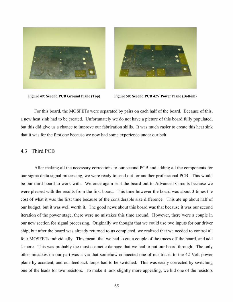
Figure 49: Second PCB Ground Plane (Top) Figure 50: Second PCB 42V Power Plane (Bottom)
For this board, the MOSFETs were separated by pairs on each half of the board. Because of this,
a new heat sink had to be created. Unfortunately we do not have a picture of this board fully populated,
but t fabrica eat sink
that it was for the first one because we now had som ur belt.
we
ere pleased with the results from the first board. This time however the board was about 3 times the
cost of what it was the first time because of the considerable size difference. This ate up about half of
our budget, but it was well worth it. The good news about this board was that because it was our second
iteration of the power stage, there were no mistakes this time around. However, there were a couple in
our new section for signal processing. Originally we thought that we could use two inputs for our driver
chip, but after the board was already returned to us completed, we realized that we needed to control all
four MOSFETs individually. This meant that we had to cut a couple of the traces off the board, and add
4 more. This was probably the most cosmetic damage that we had to put our board through. The only
other mistakes on our part was a via that somehow connected one of our traces to the 42 Volt power
plane by accident, and our feedback loops had to be switched. This was easily corrected by switching
one of the leads for two resistors. To make it look slightly more appealing, we hid one of the resistors
his did give us a chance to improve our tion skills. It was much easier to create this h
e experience under o
4.3 Third PCB
After making all the necessary corrections to our second PCB and adding all the components for
our sigma delta signal processing, we were ready to send out for another professional PCB. This would
be our third board to work with. We once again sent the board out to Advanced Circuits because
w
65
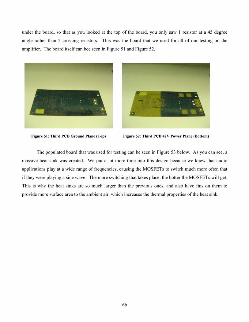
under the board, so that as you looked at the top of the board, you only saw 1 resistor at a 45 degree
angle rather than 2 crossing resistors. This was the board that we used for all of our testing on the
amplifier. The board itself can bee seen in Figure 51 and Figure 52.
Figure 51: Third PCB Ground Plane (Top) Figure 52: Third PCB 42V Power Plane (Bottom)
The populated board that was used for testing can be seen in Figure 53 below. As you can see, a
massive heat sink was created. We put a lot more time into this design because we knew that audio
applications play at a wide range of frequencies, causing the MOSFETs to switch much more often that
if they were playing a sine wave. The more switching that takes place, the hotter the MOSFETs will get.
This is why the heat sinks are so much larger than the previous ones, and also have fins on them to
provide more surface area to the ambient air, which increases the thermal properties of the heat sink.
66

Figure 53: Third PCB Fully Populated
4.4 Fourth PCB
After correcting the mistakes that were found in our third PCB, we decided to create a fourth PCB with
all the BNC connectors removed, and the board made as small as possible. We did this with the hopes
that we might be able to send out one last board, but unfortunately, we ran out of both money and time.
is however a great place to pick up from if this project gets continued in the future. The PCB is ready
to be sent out with all the mistakes already corrected in the program. Also added to the board were
twice as many bypass capacitors for the 42 Volt power source. It also was important to see how small
we could get the amplifier in size without the BNC connectors on there. They were necessary for
oubleshooting, but now that the bugs are worked out of the amplifier, they just get in the way. The
It
tr
board layout for our final PCB as well as the previous ones can be found in the appendix.
67

5 Testing and Results
In this section of the report, we will guide you through the process of how we tested various
aspects of our amplifier, and explain to you the results we obtained.
5.1 Efficiency Testing
The goal of this project was to design and build a Class-D amplifier that achieves an efficiency
of 95%. In order to determine that we met this specification it is first importan ethod of
which data can be collected. Using th d need to determine input and output
ower. This section will illustrate the tools and techniques used to determine efficiency as well as an
ine input and output power.
here are several methods by which power can be calculated, but the resources that were available to us
were slightly limited. However, by utilizing the simple equations below, we were able to determine
both input and output power of our amplifier.
t to discuss the m
e resources available we woul
p
explanation of our final results.
It was necessary to use three measurement devices in order to determ
T
VIPower *=
RVPower
2
=
Since the BK Precision regulated power supply we were using gave a current reading as well as a
voltage reading, we chose to use the P = IV equation for input power. We were somewhat limited by the
itor the input voltage directly on the board using an HP 34401A multimeter
ccurate to six significant figures.
The output power was measured using only one device at a time. For this task, we chose to use a
Tektronix TDS 210 digital real-time oscilloscope. With this device we were able to capture snap-shots
f the output waveform as shown in Figure 54.
accuracy of this device since it was accurate only to one-tenth of an ampere. On the other hand, we
would be able to easily mon
a
o
68

Figure 54: Oscilloscope Snapshot
When connected to a computer, data could be uploaded into a spreadsheet to find the RMS, or
root-mean squared, voltage. This was solved using the following equation.
n
VVAvg n
OUTi
OUT
∑=
2
2 )(
)( 2OUTRMS VAvgV =
The equation for output power was simply RO
temperature was apparently negligible because the load resistance measured to be the same at both
ambient room temperature and at 140°F.
Finally, the ratio of input and output powers was solved for and recorded as the percentage
efficiency of the amplifier.
VP RMS2
= . The change in resistance due to
[%]IN
OUT
PPEfficiency =
The efficiency in comparison to clock speed of the Sigma-Delta Modulation was our most
critical measurement. This relation is essential in determining the sampling frequency at which yields
69

the highest efficiency. By using a HP33120A to generate an array of clock waveforms we were able to
graph the results at several frequencies ranging from 250 kHz to 4 MHz. Figure 55 below shows the
results of these tests.
Efficiency vs. Clock Speed
78.00%
80.00%
82.00%
84.00%
86.00%
88.00%
90.00%
92.00%
Effic
ienc
y
94.00%
98.00%
0.00 0.25 0.50 0.75 1.00 1.25 1.50 1.75 2.00 2.25 2.50 2.75 3.00 3.25 3.50 3.75 4.00 4.25
Clock Speed [MH
96.00%
z]
0% Clipped, 1.4Vin 40% Clipped, 1.6Vin 100% Clipped, 3.0Vin
Figure 55: Efficiency vs. Clock Speed
pped sinusoidal input. This produces the least efficient case since the
utput never reaches the rails of the supply. Therefore switching occurs at each clock pulse in order to
represent a median value. The second case was taken with a 40% clipped input signal. At this
condition, little or no switching takes place nearly 40% of the time. While no switching is taking place,
no error can be apparent with the output at the rail, thus the Sigma-Delta Modulation does not send a
correcting signal. The final case utilized for these results uses a fully clipped input signal. For this case,
the output is either high or low during each half cycle of input, switching is at a minimum. Nearly all
switching loss is therefore avoided and maximum efficiency is obtained. This proves that we do in fact
meet our expected 95% efficiency.
Efficiency is shown here under three different input conditions in addition to clock speed. The
first condition uses an un-cli
o
70
There are other factors that affect efficiency. Since the 42 Volt PowerNet standard states that all
vehicles should run at a charging voltage of 48 Volt, we decided to test our amplifier in that state. Using
a fully clipped input signal we were able to achieve a maximum of 97.4% efficiency. The larger
efficiency is due to the increase in voltage and was noted to be due to the standard specifications.
Lastly, using the correct value for the dead-zone resistor is important when optimizing efficiency and
will be explained in the following section of this report.
5.2 “Dead-Zone” In order to achieve a clean output, the signal processing circuit must be properly calibrated. For
a closer look at the components involved see the section on Sigma-Delta. One of the first items that
must be taken into account is the dead-zone resistor, Rdz. It determines the voltage that each
parator sees on its negative input. Finding the ideal resistor value is a multilevel process beginning com
with the calculation of the integrator time constant, τint. The following equations are given knowing the
transfer function of a Miller integrator discussed in the Sigma-Delta section of this report.
intintint CR=τ
)1000)(24(int pFkΩ=τ
sec150int u=τ
The corresponding dead-zone voltage would then be easily
o
calculated as the voltage that the
utput of the integrator would swing during this time. Our first calculations to find an accurate dead-
zone resistor are seen below.
t
inripple eVV −−=
−
)1( /τ
)ripple eVV −= 1(5 2/7.6 MhzkHz
VVripple 05.0=
71

Figure 56: Ideal Integrator Output
Figure 56 shows the ideal integrator output and how given the correct VDZ there should be no overlap of
MOSFET switching and minimal crossover distortion. Therefore the dead-zone voltage is half this total
swing.
VVV rippleDZ 025.021
==
The dead-zone resistor is therefore the value that completes the ratio:
kDZ
DZ
rail
DZ
RRR
VV
100−=
Ω= 5.167DZR
It is also important to mention how to calculate VDZ given a Vrail of 15V, RDZ, and R100k.
kDZ
DZrailDZ RR
RVV100−
=
72

However when implemented in the circuit, this did not give us the results that we were looking to
achieve. The output of the tri-level sigma-delta modulation scheme should be two waveforms that
should nearly overlap at low voltages to avoid crossover distortion and not result in clipping at the
output. With a dead-zone that is too small, outputs of the flip-flop will be too active. This decreases the
efficiency of the scheme greatly since it leads to the greatest amount of switching. On the other hand, a
value too great would result in cross-over distortion.
Figure 57: Vdz = 7.5mV (Too Small), f = 1kHz
input. This leads to a period when the outputs are both zero. The problem with crossover distortion is
that this greatly affe
Cross-over distortion is caused by too great a dead-zone voltage seen by the comparator negative
cts performance at lower volume since the dead-zone is a large portion of a small
put <100mV. This distortion can be seen in Figure 58 and Figure 59. When the input voltage is near in
zero, the filtered output looses its sinusoidal shape and flat-lines causing cross-over distortion for a small
time duration.
73

Figure 58: Vdz = 150mV (Too Large), 1kHz Figure 59: Vdz = 150mV (Too Large), 10kHz
can say that there was a distinct difference in noise level between each of the dead-
ones depicted above. Additionally, a signal processing scheme equipped with a larger dead-zone was
ercentage of noise at low input voltage levels. This is due to the fact that
gnal-to-noise ratio is calculated as
The theory behind the dead-zone voltage states that the noise in the output is regulated by the
amount of crossover distortion. Since crossover distortion is clearly a result of an inaccurately tuned
dead-zone, one can state that output noise is proportional to dead-zone voltage. Although we lacked the
time to perform accurate signal-to-noise tests with several dead-zone voltages, listening tests were a
second option. We
z
susceptible to a greater p
si ⎟⎟⎠⎝ NOISEV
smaller dead-zone.
The perfect dead-zone voltage was found by plugging and checking several resistor values in
order to find where the crossover gap shrinks to zero and minimal overlap switching occurs.
⎞⎜⎜⎛ SIGNALVlog10 .25 This noise would emphasize the need for a
This
oltage value was 50mV. Figure 60 and Figure 61 depict the ideal results given when using this value.
v
74
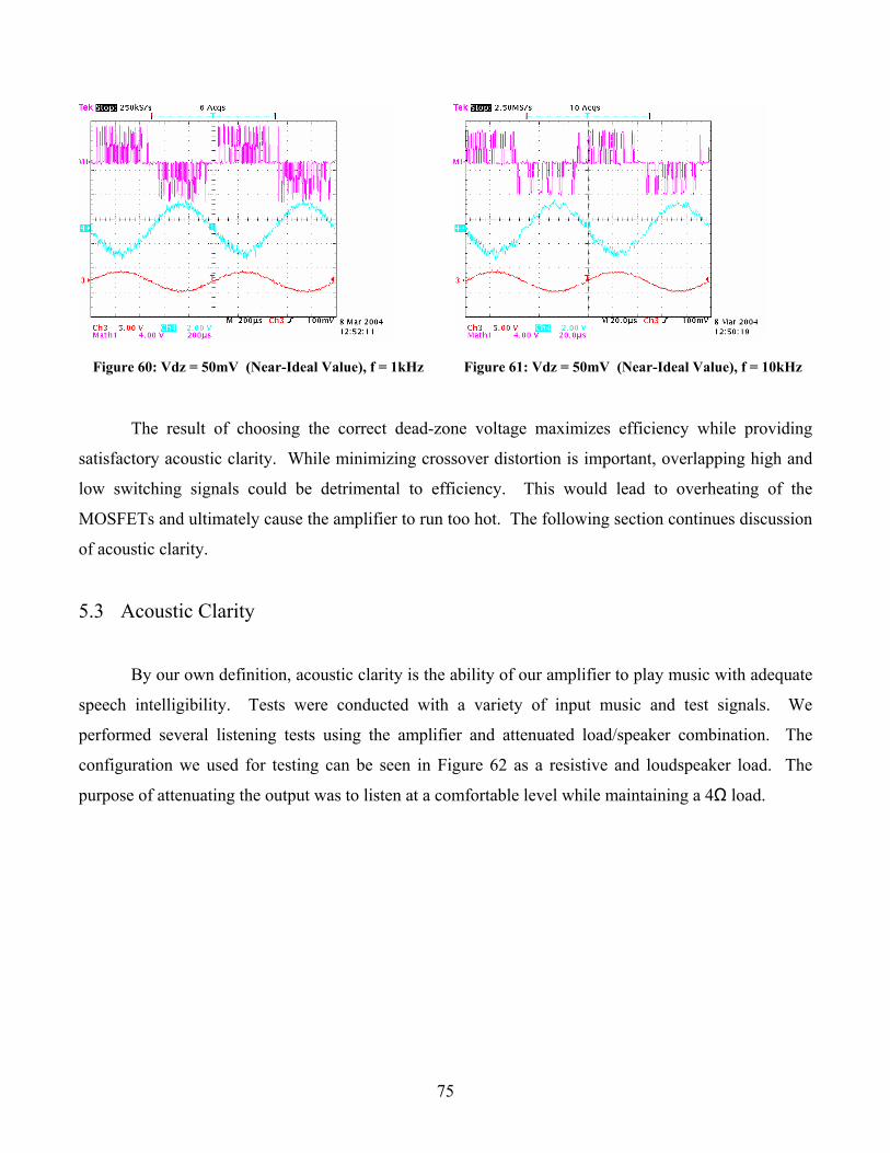
Figure 60: Vdz = 50mV (Near-Ideal Value), f = 1kHz Figure 61: Vdz = 50mV (Near-Ideal Value), f = 10kHz
The result of choosing the corr maximizes efficiency while providing
.3 A
ect dead-zone voltage
satisfactory acoustic clarity. While minimizing crossover distortion is important, overlapping high and
low switching signals could be detrimental to efficiency. This would lead to overheating of the
MOSFETs and ultimately cause the amplifier to run too hot. The following section continues discussion
of acoustic clarity.
5 coustic Clarity
By our own definition, acoustic clarity is the ability of our amplifier to play music with adequate
speech intelligibility. Tests were conducted with a variety of input music and test signals. We
performed several listening tests using the amplifier and attenuated load/speaker combination. The
configuration we used for testing can be seen in Figure 62 as a resistive and loudspeaker load. The
purpose of attenuating the output was to listen at a comfortable level while maintaining a 4Ω load.
75

Figure 62: Speaker Test
Although listening tests were satisfactory, there was a slight “hiss” in the output. To view the
noise, we displayed an FFT of the output. This noise had a constant magnitude regardless of input
signal, so it was determined to be internally generated. In order to maximize the signal-to-noise ratio, it
was best to leave any CD player or other dev e speech intelligibility was
back. There are a few culprits that have been identifies as candidates for the hissing
noise at our speaker. The first are improperly calibrated resistor networks used as voltage dividers using
5% resistors. In practice it is best to use special resistor network packages calibrated to less than a
ice at full volume. At low volum
greatly degraded.
According to our system design, noise should have been stopped from reaching the load. In one
respect, any high-frequency (EMI) would be filtered by a two-pole Butterworth filter. On the other
hand, anything below our sampling rate should also be compensated by the time it reached the output
with negative feed
percent. Secondly, Texas Instruments LF356 operational amplifiers were used in place of more
expensive types. In a final board design these components would be swapped with more precise and
faster slewing chips.
5.4 Output Power Due to the fact that this MQP was about creating an audio amplifier, we thought it was necessary
to show that the project we constructed actually had the ability to amplify a signal. After testing several
76

different areas of the amplifier, we were able to capture an oscilloscope output of one of our tests. This
output can be seen in Figure 63 below.
Figure 63: Input vs. Output
What you can see from the picture is an input sine wave at 5 Volts per division on the scope and
an output sine wave at 25 Volts per division. What you can’t see is that the test input signal was an 800
z sine wave with amplitude of 1.4 Volts. The output waveform was measured to have amplitude of 40
f our amplifier, you can simply divide the output power by the input
ower as shown.
H
Volts. To determine the gain o
p
57.284.1
40===
InputOutputGain
As you can see, the gain of our amplifier is approximately 30. This gain factor can be decreased
at our discretion by adjusting the feedback discussed in the Sigma-Delta section of this report. This gain
of 30 that we obtained was determined using the specifications of a CD player maximum output value of
1.4 Volts. Because this was a maximum value, we wanted a signal of equal magnitude to have the
bility of playing through our amplifier without clipping. As you may recall, the voltage rails that we
are using are 42 Volt. Based on Figure 63, the output is only 2 Volts from reaching the rails of our
plifier, which would result in a clipped output. Other adjustments could have been made to achieve a
a
am
77

greater gain if the input signal was attenuated, however we felt that the maximum value out of a portab
CD player was adequate for our testing purposes.
We also want
le
ed to know how much power our amplifier was able to produce. To do this, we
ported the data from the oscilloscope to our computer as mentioned in Efficiency section of this
report. Using the same Microsoft Excel spreadsheet, we were able to compute the RMS power of our
amplifier. To recap, the formula we used was:
im
RVPower
2
=
Using the same input of an 800 Hz sine wave of amplitude 1.4 Volts, we were able to measure a
power output of 400 Watts RMS when 42 Volt supply rails were used. We were very pleased with the
results, and met our goal of creating a high powered amplifier. Perhaps 400 Watts was slightly more
power than necessary, but it granted us great satisfaction in knowing that the amplifier we produced is
capable of competing with other amplifiers on the market.26
Referring to Figure 63 once again, notice that the output remains in phase ith the input. This is
portant because in car audio a is used to only power the front
idea is that you want the output power to be much
greater than that of the noise power in order to have a clean sounding amplifier. If the noise power is
small enough compared to the output power, then it will not be audible to the human ear at the output.
The SNR more simply is the ratio of signal power to noise power. This formula can be seen below.
w
im pplications, often times an amplifier
speakers in the automobile. If the output was out of phase with the input, then the result would be rear
speakers that were playing out of phase with the front speakers, resulting in poor sound quality and noise
cancellation.
5.5 Signal to Noise Ratio
When looking at industry standards, one specification given on almost every amplifier is a
signal-to-noise ratio. This specification indicates how much noise is created in the amplifier relative to
the signal you are trying to pass through it. The
Noise
Signal
PP
SNR =
78

In order to compute the SNR, an FFT of the output must first be examined. For our amplifier,
we used an 800 Hz sinusoidal input with amplitude of 1.4 Volts. We then examined the output, as seen
in Figure 64 below.
Figure 64: FFT used to obtain SNR
The oscilloscope that we used for testing was a Tektronix TDS-210. One of the features that
made this scope easy to work with that it has an output that allowed us to import data into the computer.
The data was imported into Microsoft Excel, where we were able to use the data to compute the power
of both the signal and noise. To do this, we had to first separate the signal power from the noise power.
equations below show the
That was done by observing the large magnitudes that occurred around 800 Hz where the spike was
apparent. Everything else was considered to be noise in our system.
With the signal and noise magnitudes separated, the total power in each was found. This was
done by converting all of the data from decibels into watts of power. The
correlation between decibels and watts of power.
1012
1210
1010
10log10
dBP
Wa
WattsdB
P
PP = −
tts ×= −
79

All of the signal and noise powers were then summed separately. Because the SNR is simply a
ratio of the two powers, the SNR was easy to calculate at this point. With the information obtained from
the FFT, we determined that our am ier had a SNR of 43dB using the next equation.
plif
Noise
SignaldB W
WSNR log10= .
ssibly
locate the noise in our system. Some of these suggestions are listed in the Recommendation section of
this report.
5.6 Efficiency Loss The primary goals of this MQP were the design of a high-power ultra-efficient Class-D amplifier
and the analysis of why 100% efficiency is not possible. While the design of the amplifier was
instrumental in completing a successful project, the first objective was not as much of a major concern
as the second one. Hours were spent doing research and testing of why an amplifier is not capable of
100% efficiency.
In theory, the Class-D design shou as much power as it receives. Thanks to
OSFET switching devices, this technology is able to approach this echelon closer than any other
previou
into these specifications was done in the Background section of this report.
Before
Typically in the market, you will find amplifiers that range from 80dB – 120dB for a SNR. Our
amplifier is much less, and as a result there is an apparent “hissing” noise at the output. If more time
were permitted, there are several things that could be done to try and increase the SNR, or po
ld be able to output
M
s design. Neither Class-A nor Class-AB boasts efficiencies above 50 or 80% respectively.27 The
theory behind this is illustrated in the What is Class-D section of this report.
The method by which efficiency would be maximized would be to first find the most ideal
MOSFET switches. Since ideal switches do not exist, there are a few specifications that require special
concern. A closer look
one can name these categories, it is prudent to look at the equations that govern power loss in
switches. These equations are found in Table 5.
80

][**)( WattsfVQSourceGateowerLossSwitchingP clkgsg ==− ][)(21)( WattsfttIVSourceDrainowerLossSwitchingP sOFFONoin =+=−
( )2
2 2*..
2/2
*2
2..
][2/*)(
dsds
dsLoad
dsds
dsLoad
ds
dRds
RVLC
RRVV
RRRLC
WattsIVLossDCConduction
=
⎥⎦
⎤⎢⎣
⎡+⎥
⎦
⎤⎢⎣
⎡⎟⎟⎠
⎞⎜⎜⎝
⎛+
=
==
dsloadds
rail
DCsgswsdsw
loss
PPPPtotalP
Efficiency
)(
2*100100
,, ++
−=
−−
22 dsLoad RR +R
RRV
Efficiency
**2
2*100100 2
⎟⎟⎠
⎞⎜⎜⎝
⎛+
−=
Table 6: Power Loss and Efficiency Equations
These important specifications are therefore RDS and QG. This is discussed in the Background
section on efficiency but is important to note that both RDS and QG should be minimized. These two
factors greatly affect efficiency and follow the following power loss curve as shown in Figure 65.
Figure 65: Powe Loss
Our decision to select the Fairchild FDP038AN06A0 PowerTrench MOSFET was based on
finding the perfect match for our application. We needed a device with at least a 60 Volt break down
voltage and a 50 Amp continuous current limit based on a 1Ω load. Since we found that with higher
break down voltage, RDS increased, we chose a MOSFET with a break down voltage at our bare
minimum of 60 Volts.
Other decreases in efficiency are due to the filter components. Losses from either the capacitors
r are either conductively or in their AC characteristics.
A primary concern in our filter design was the inductors. After calculating the appropriate
values for these components, we needed to send our specifications to a custom winding company for
r
or inductors can be calculated using several known equations given throughout this section. Methods by
which these elements dissipate powe
81

manufacture. Each inductor had to withstand the same amount of current as each MOSFET. Using a
1Ω resistive load, this current would peak to 50 Amps at 50 Volts. Therefore, above average gauge wire
had to be used. The windings were made with 10 gauge wire and RDC of less than 20mΩ. Now that all
the conduction loss resistances are known, the total conduction loss can be calculated from the
MOSFET, inductor, and load values.
( )( ) ( )( )( )( )
( )( )( )
Wmm
mmRRRRRVLC
VRRLC
WattsIVLossDCConduction
inductorMOSGETrail
u r
ddrop
13.5208.324
208.32*4222*..
2.
][*)(
2
2
2
2
=Ω+Ω+Ω+Ω
=+++
=
⎥⎦
⎤⎡⎤⎡ ⎞⎛ +
==
Some additional power loss is due to the capacit r would be lossless and
return each bit of energy it had stored. However, the ESR (Equivalent Series Resistance) rating of a
capacitor is a particular evaluation of quality given to each series of manufactured devices. Ideally this
value would be zero and therefore would have no AC resistance. In order to calculate the ESR for a
given capacitor, one must start by finding its dissipation factor. In our case, we used capacitors with a
dissipation factor of < 1% @ 20°C at 1 kHz. Using a value of 1% and the following equations, we can
lve for the ESR at a switching frequency of 192 kHz.
RRRV
RRR ind ctoMOSGETLoad
railrail
inductorMOSGETLoad
inductorMOSFET
2*
2. ⎢
⎣ ++⎥⎦
⎢⎣
⎟⎟⎠
⎜⎜⎝ ++
=
inductorMOSGETLoad
ors. A perfect capacito
so
XcESR
=δ
CfXc
π21
=
CfESR
πδ
2=
Ω== mkHzuF
ESR 83)192)(1.0(2
01.π
ESR is not constant and changes greatly with frequency. Figure 66 shows the ideal and actual
impedance of a 0.01 µF capacitor.
82

Figure 66: Actual vs. Ideal 0.01uF Capacitor Impedance28
Using the equations for current and ESR, the power dissipated in the capacitors can be found.
dtdVCI =
OfVCI **∆=
)192(*)84(*)1.0( kHzVuFI =
AI 6.1=
WmAofcapsRIP 4.316)83*9.12()*#( 22 =Ω==
Figure 67 shows power loss versus dissipation factor. This is very helpful when determining
how much loss is acceptable when selecting capacitors.
83

Figure 67: Power Loss vs. Dissipation Factor
Additionally, we have plotted the power loss versus switching frequency since we have a very dynamic range of switching frequencies that may be encountered during audio amplification. See Figure 69.
Power Loss vs. Switching Frequency
0
5
10
0 200,000 400,000 600,000 800,000 1,000,000 1,200,000 1,
15
20
25
30
35
40
400,000 1,600,000 1,800,000 2,000,000
Pow
er L
oss
[Wat
ts]
Switching Frequency [Hz]
Figure 68: Power Loss vs. Switching Frequency
84

Theoretical calculations are extremely difficult for MOSFET switching, conduction, and filter
losses in an amplifier that use Sigma-Delta Modulation. This is due to the fact that the actual number of
itches per cycle of an input signal is not known. The amount of switching that occurs corresponds to
the size of the “dead zone.” The “dead-zone” is described in its own section of this report. Also, input
signal size has an affect on the efficiency. On one extreme, much too large an input will result in
clipping and minimal switching. In this case, the MOSFET devices need only to switch twice per cycle.
On the other hand, a small input signal creates the most uncertainty in the output and maximum amount
of switching will occur. In this case or any in between, the number of switches per cycle is not known.
In order to demonstrate this, we have plotted the “ideal” efficiency versus switching frequency in Figure
69 using the equations in Table 5.
sw
Efficiency vs. Clock Speed
0.0%
10.0%
20.0%
30.0%
0.00 0.25 0.50 0.75 1.00 1.25 1.50 1.75 2.00 2.25 2.50 2.75 3.00 3.25 3.50 3.75 4.00 4.25
Clock Speed [MHz]
40.0%
50.0%
60.0%
70.0%
80.0%
90.0%
100.0%
Effic
ienc
y
Constant Switching Clipped 800Hz Signal
Figure 69: Efficiency vs. Switching Speed
The results are as predicted. The efficiency of a constantly switched output is very poor and
ecreases linearly due to the frequency that the MOSFETs switch. Conversely, if the input signal is
large and the output is clipped, the efficiency remains at 99.8%.
We decided to plot our actual efficiency results using three different input conditions on the
same axis as the predicted results. The first case was an unclipped 800 Hz sine wave. The second signal
d
85

was clipped 40% of the time. Finally, the last was a 100% clipped sine wave, or essentially a square
wave. This is plotted in Figure 70.
Efficiency vs. Clock Speed
0.00%
10.00%
20.00%
30.00%
40.00%
50.00%
60.00%
70.00%
80.00%
90.00%
100.00%
ficie
ncy
0.00 0.25 0.50 0.75 1.00 1.25 1.50 1.75 2.00 2.25 2.50 2.75 3.00 3.25 3.50 3.75 4.00 4.25
Clock Speed [MHz]
Ef
0% Clipped, 1.4Vin 40% Clipped, 1.6Vin 100% Clipped, 3.0VinConstant Switching Clipped 800Hz Signal
Figure 70: Efficiency vs. Clock Speed
By analyzing the two simultaneously, we can see that the theoretical efficiency is lower than that
obtained. Clearly something is happening that prevents the measured efficiency from dropping below
the theoretical efficiency. The fact that the output MOSFET switches are not being toggled during each
clock tick like in some configurations is not shown here. The only real data that we can abstract is a
difference of nearly 5% difference in efficiency between an ideally clipped and actually clipped output.
This would suggest that much more loss is due to conduction than expected. In fact, this would explain
the warming of the MOSFET switches at high current. If this 5% were to be explained by a direct series
resistance, that value would be 221mΩ solved for in the next few equations.
LOADequiv
equiv
RRR
Efficiency+
=
Ω= mRequiv 221
86

Based on the fact that this amplifier was able to reproduce an unclipped sine wave at 92%
atts of power loss, would suggest a maximum number of 3.5 million switches per
75 MHz at theoretical conditions. These values can be found using Figure 68
efficiency, 32 W
second or 1.
The factors mentioned in this section have played a major part of determining the efficiency of
our amplifier design. In summary, the lack of lossless capacitors, wires without resistance, and perfect
MOSFET switches can not be avoided. Because we had a fairly large budget, we found the components
that were most detrimental to our efficiency goals and purchased the best components we could find to
reduce efficiency loss.
87

6 Recommendations
Now that the project is completed, we recognize that there are some things that could have been
done differently. There are areas for improvement in all stages of the design. This section will focus on
ideas that could be implemented into the amplifier to improve upon the existing design.
The first recommendation if this project is continued is that a DSP chip should be used to control
the signal processing. There are several reasons for this. DSP technology has been a fiercely growing
application in audio. Many home entertainment units and even car audio amplifiers now use this
technology. The benefits are numerous as the possibilities of signal processing with DSP are nearly
limitless. First, is that the signal to noise ratio would be much higher, resulting in a clean
output. The cleaner sounding output is made by the much higher switching speed of the amplifier.
er sounding
ore if
er output, but as you might expect
at every integrator added to the
rcuit creates another pole. To balance this, an equal number of zeros must be added to keep the system
stable. Second, potentiometers could be used instead of resistors from the input signal to control the
volume of the amplifier or to add a high or low-pass crossover.
Typically, Class-D amplifiers are not used for full-range audio applications, but if the application
requires a small frequency bandwidth, there is no reason to make the amplifier do more work than it has
to. Our amplifier was designed to reproduce the full audible bandwidth of 20-20 kHz. If this was not
such a stringent requirement, a lower switching speed could be used to further push the efficiency
limitations. Lastly, all the components in the amplifier were designed for a 50 Amps maximum current
draw. By reducing the impedance of the load, the amplifier may be tested at these more extreme levels.
Theref quantization noise can be pushed into the megahertz band, filtering becomes simpler and
noise in the audible band is negligible. Second, DSP processors are often equipped with multiple analog
and digital inputs that may perform other tasks besides Sigma-Delta Modulation. With the use of a DSP
chip, external controls could be implemented into the amplifier. For example a digital keypad could be
part of the design where the user could control the volume, crossover, bass boost, or other added features
into the amplifier.
If DSP is not the method of choice, then there are other options as well. First, a higher ordered
Sigma-delta modulator could be used. This means that the feedback taken from the load would go
through several integrators instead of just one. This creates a clean
adds a great deal of complexity to the circuit. One thing to note is th
ci
88

While the components in our amplifier were designed to be able to run at a 1Ω load, the system will
ecome
plifier could be
-amp. While many of these upgrades would cost significantly more money, their non-
b unstable. The reason for this is because the inductors that were purchased for the project were
very costly, and in order to push the poles further from each other, a different inductor value would have
to have been chosen. By redesigning the filter, it is possible to achieve a phase margin of greater than
45° at a 1Ω load. It is imperative that these inductors be similarly rated for 50 Amps of current.
At the very least, a future MQP group could improve our current signal processing circuit in a
few ways. The first and most immediate impact would be to compare several different operational
amplifiers. While the LF356 model chip used in our circuit is widely accepted for many applications,
there are new technologies that deserve to be explored. Many of these technologies boast low-voltage
offset, less jitter, and higher slew rates. These op-amps would be more able to accurately reproduce
high frequency noise which would allow for more noise to be filtered out. If information is lost in
translation through these devices, the risk of noise slipping through is greatly increased.
Lastly, many basic components used in the signal processing portion of the am
replaced with more finely tuned values. These include both resistor and capacitor values and ratings.
Many parts were used because of their accessibility through the WPI ECE Shop with short notice.
Capacitors were all special ordered but their values were determined by manufactures’ data sheets only.
Larger bypass capacitors may reduce the noise due to instant current demands and they may also
increase stability. Resistor packages are available that deviate less than 1% of the measured value and
they could be used as input to the instrumentation amplifier or differential feedback attenuator.
Additionally, instrumentation amplifiers are available that would replace the need for these resistor
packages and op
monetary value may make them worthwhile.
89

7 Conclusions ructed, and tested that met
ching
er a 100% clipped input sine
al about using a fully clipped input signal to
ved
ply. From the measurements
yield the highest
tandard. With
voltage that
ill occur in a real-life car application. The amplifier was tested from 48 Volts all the way down to 30
Volts to observe the amplifier's response. The amplifier acted just as intended and the output power did
r the swing in voltage.
g an amplifier unless the output is an amplified
ing a 4Ω speaker with a max power of 500 Watts
from the speaker was apparent but
s noticeable. The noise is largely due to the trade-
oltage. With a dead-zone voltage too high, acoustic clarity gets
iency goes up. For the opposite case, with a really small dead-zone voltage, acoustic clarity
The dead-zone voltage that suited the amplifier's purposes the best
mplifier that has been constructed could be marketable with a little
plifier currently has a footprint size of only 29 square inches, making the power to
uch higher than that of other amplifiers on the market. If more time was allowed to be spent
or the amplifier, the amplifier could be
e in an automobile regardless of a vehicle’s central computer location. This would also
rketable.
This project was deemed a success. An amplifier was designed, const
all of the project goals. The first project goal to mention is the fact that amplifier is capable of rea
95% efficiency. The goal was surpassed when the amplifier was tested und
wave, at 800 Hz, using a 42 Volt supply. If you are skeptic
achieve a maximum efficiency, we are pleased to announce that an efficiency of 92% was achie
using a purely sinusoidal input at 800 Hz once again with a 42 Volt sup
taken of our amplifier, it was determined that a clock speed of 1.5 MHz would
efficiency. Another project goal was to design the amplifier around the 42 PowerNet S
that said, the amplifier must also maintain a constant power throughout the fluctuations in
w
not change more than 3 Watts ove
In the audio world, there is no point in makin
version of the input. Our amplifier was capable of driv
and an RMS power of 400 Watts. At low volumes, the noise coming
a me less and less the volume increased the noise beca
off that is made with the "dead-zone" v
lost but effic
improves but the efficiency suffers.
was 50 mVolts.
Lastly, it is believed that the a
more time. The am
size ratio m
on the design of an EMI shield that would double as a heat sink f
located anywher
make the amplifier very ma
90

8 References Beranek, Leo L. Acoustics. New York: Acoustical Society of America, 1996.
Boylestad, L. Nashelsky. Electronic Devices and Circuit Theory. New Jersey: Prentice Hall, 1992
Haag, Michael. Understanding Pole/Zero Plots on the Z-Plane. July 2003,
<http://cnx.rice.edu/content/m10556/latest/>
Incropera & DeWitt. Introduction to Heat Transfer 4th ed. New York: John Wiley & Sons, Inc. 2002
Mohan, N . Power Electronics and Drivesed . Minnesota: MNPERE, 2003.
Pohlmann, K.C. Principles of Digital Audio, 3rd ed. New York: McGraw-Hill, 1995.
Robichaud, Jon. Interview. Heat Transfer & Metal Properties. Leominster, 23 Sept. 2003
Sedra & Smith. Microelectronic Circuits 4th ed. New York: Oxford University Press, 1998.
1 http://www.cpemma.co.uk/pwm.html 2 www.xta m/html/products/xtant1. 3 http://www.numerix-dsp.com/appsnotes/APR8 elta.pdf 4 http://skyvision.com/pages/informatio nte tml#t7 5 http://www.epanorama.net/documents o/6 http://www.sci-worx.com/internet/bor foru ll.pdf 7 http://foc i.com/docs/prod/productf .jhtml ericPartNumber=PCM18 Class D Au io Amplifier
nt.co-sigma-d
r/hdtvfaq.hspdif.html
m/bnvius.t ?gen
d
1i.cfm
n_ce/audidnetzolder 738
, WPI MQP, 9 http://www.web-ee.com/primers/files/DesignSem f 10 http://www.t ath.com/downloads/a df 11 Incrop itt , p53 12 Robicha13 http://www.diamondman.com/usesb3.htm 14 Mohan, 15 http://www.fairchildsemi.com/whats_new/30 .html 16 Pohlm 54. 17 See Ap Efficiency Calculations 18 Sedra & Smith, p76. 19 Sedra & Smith, p89. 20 Haag, p21 Haag, p2. 22 Ogata, Katsuhiko, Modern Control Engineeri ice Hall, 2002, p539. 23 Beranek . 395. 24 www.4p com 25 Beranek 253. 26 Appendix lifier research 27 Boylestad, ch15. 28 http://newson-consulting.com/emi-capacitors.htm
2003
n11.p3.pd
ripera & DeW
ud
p2-9vauto_nph
ann, p1pendix on
1.
ng, Prent, pgcb., pg
Amp
91
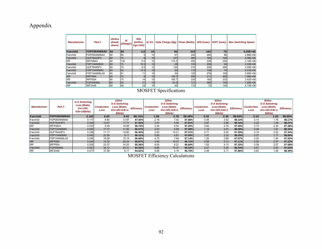
Appendix
Fairchild FDP038AN06A0 60 80 3.8 10 95 310 163 75 4.20E+06Fairchild FDP050AN06A0 60 80 5 10 61 245 264 86 2.86E+06Fairchild HUF76443P3 60 75 8 10 107 260 195 100 3.39E+06IRF IRFP064V 60 130 5.5 10 173.3 250 226 250 2.10E+06Fairchild FDP10AN06A0 60 75 10.5 10 28 135 206 94 3.33E+06Fairchild HUF76445P3 60 75 6.5 10 124 310 205 295 2.00E+06Fairchild FDP13AN06A0 60 62 13.5 10 22 115 158 74 4.31E+06Fairchild FDP14AN06LA0 60 61 11 10 24 125 276 109 2.60E+06IRF IRFP064 60 70 9 10 126.7 300 211 300 1.96E+06IRF IRFP054 60 70 14 10 106.7 230 180 233 2.42E+06Fairchild FQP50N06L 60 52 21 10 24.5 121 380 145 1.90E+06IRF IRFZ44E 60 48 23 10 40 110 72 140 4.72E+06
Rds (mOhm,
Vgs=10V)at Vin Gate Charge (Qg) Pmax (Watts)Manufacturer Part #
Vbrdss (break down)
Id (25degC) tON (nsec) tOFF (nsec) Max Switching Speed
MOSFET Specifications
Conduction Loss
D-S Switching Loss (Watts,
Vin=10V,fclk=192kHz)
Efficiency Conduction Loss
D-S Switching Loss (Watts,
Vin=10V,fclk=192kHz)
Efficiency Conduction Loss
D-S Switching Loss (Watts,
Vin=10V,fclk=192kHz)
Efficiency Conduction Loss
D-S Switching Loss (Watts,
Vin=10V,fclk=192kHz)
Efficiency
Fairchild FDP038AN06A0 0.182 6.60 9.52 98.14% 1.66 4.78 98.49% 0.42 2.39 98.64% 0.10 1.20 98.65%Fairchild FDP050AN06A0 0.117 8.65 13.97 97.40% 2.18 7.02 97.88% 0.55 3.52 98.10% 0.14 1.76 98.17%Fairchild HUF76443P3 0.205 13.67 11.71 97.05% 3.47 5.90 97.81% 0.87 2.96 98.16% 0.22 1.48 98.27%IRF IRFP064V 0.333 9.49 18.98 96.70% 2.40 9.54 97.20% 0.60 4.78 97.40% 0.15 2.40 97.38%Fairchild FDP10AN06A0 0.054 17.77 11.85 96.57% 4.53 5.99 97.58% 1.15 3.01 98.08% 0.29 1.51 98.32%Fairchild HUF76445P3 0.238 11.17 19.90 96.40% 2.83 10.01 97.01% 0.71 5.02 97.28% 0.18 2.52 97.34%Fairchild FDP13AN06A0 0.042 22.58 9.11 96.31% 5.80 4.61 97.60% 1.47 2.32 98.25% 0.37 1.17 98.56%Fairchild FDP14AN06LA0 0.046 18.58 15.19 96.08% 4.75 7.68 97.14% 1.20 3.86 97.67% 0.30 1.94 97.92%IRF IRFP064 0.243 15.32 20.24 95.87% 3.90 10.21 96.72% 0.98 5.13 97.11% 0.25 2.57 97.22%IRF IRFP054 0.205 23.37 16.20 95.36% 6.00 8.21 96.68% 1.52 4.13 97.32% 0.38 2.07 97.58%Fairchild FQP50N06L 0.047 34.12 20.31 93.56% 8.88 10.37 95.53% 2.27 5.24 96.54% 0.57 2.63 97.03%IRF IRFZ44E 0.077 37.08 8.17 94.62% 9.69 4.18 96.76% 2.48 2.11 97.86% 0.63 1.06 98.39%
Manufacturer Part #
2Ohm 4Ohm 8Ohm1OhmG-S Switching Loss (Watts,
Vin=10V, fclk=192kHz)
MOSFET Efficiency Calculations
92
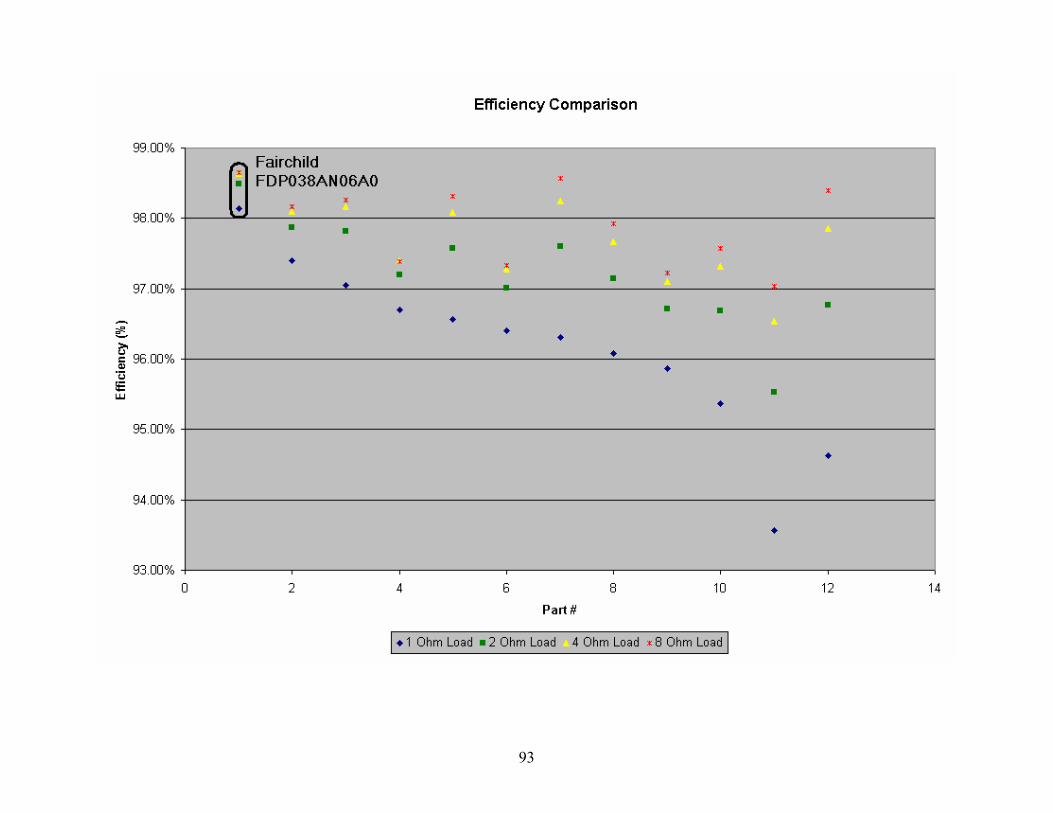
93

94
MOSFET Efficiency Equations
][1 Hztt
ngSpeedMaxSwitchifallrise
=+
=
( )2
2
222*..
2/2
*2
2..
][2/*)(
dsLoad
dsds
dsLoad
dsds
dsLoad
ds
dRds
RRRVLC
RRVV
RRRLC
WattsIVLossDCConduction
+=
⎥⎦
⎤⎢⎣
⎡+⎥
⎦
⎤⎢⎣
⎡⎟⎟⎠
⎞⎜⎜⎝
⎛+
=
==
][**)( WattsfVQSourceGateowerLossSwitchingP clkgsg ==− ][)(21)( WattsfttIVSourceDrainowerLossSwitchingP sOFFONoin =+=−
a) Maximum Switching Speed [Hz] – the fastest a device can switch on and off based on its rise
time and fall time. Since Hertz is simply the reciprocal of time in seconds, we can calculate the maximum switching speed by adding the rise and fall times and dividing 1 by this number.
b) Conduction Loss (DC) [Watts] – power loss due to current flowing from the drain to source of a MOSFET device. This equation assumes DC current or current that is steady. In order to calculate DC loss, we can begin with the equation P=I*V where V is the rail voltage and current is the drain-source current. Since we are only concerned with one of the MOSFETS, we can divide by 2. The voltage across each MOSFET is given by the ratio of its resistance relative to
the resistance of the load, dsLoad
ds
RRR
22+
. The drain-source current is then the ratio of the rail
voltage over the total resistance of the MOSFETs and the load, dsLoad
ds
RRV
2+. The simplified
conduction loss equation can be found in the table above. c) Switching Power Loss (Gate-Source) – power loss due to the charging of the gate-source
capacitance of the system in order to reach the gate-source voltage. This can be found by multiplying the gate charge (Qg), gate-source voltage (Vgs), and switching speed (fclk).
d) Switching Power Loss (Drain-Source) – power loss due to the charging of the drain-source capacitance of the system in order to reach the drain-source voltage. Equation was taken from Power Electronics and Drives, p2-9

0
500
1000
1500
2000
2500
025
5075
100125
150175
200225
250
Footprint Size [Sq. In]
Max Power [RMS Watts]
Our A
mplifier
Com
petitionC
ompetition B
est Fit
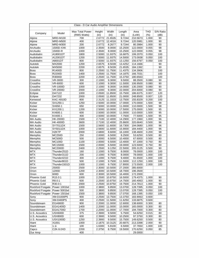
Company Model Max Total Power (RMS Watts)
Height (in)
Width (in)
Length (in)
Area (LxW)
THD (%)
S/N Ratio (dB)
Alpine MRD-M100 700 2.6772 21.6535 9.7244 210.5673 1.000 90Alpine MRD-M500 400 2.6772 12.4016 9.7244 120.5981 1.000 90Alpine MRD-M300 200 2.6772 8.2677 9.7244 80.3984 1.000 90ArcAudio 1500D-XXK 1000 2.3500 8.0000 15.2500 122.0000 0.055 98ArcAudio 1500D-R 1000 2.3500 8.0000 15.2500 122.0000 0.055 98Audiobahn A18001DT 1800 2.5000 11.9375 16.6875 199.2070 0.050 100Audiobahn A12001DT 1200 2.5000 11.9375 14.5000 173.0938 0.050 100Audiobahn A8001DT 800 2.5000 11.9375 13.1250 156.6797 0.050 100Autotek MX2000 1200 2.6575 8.5039 13.4252 114.1666 90Autotek MX5000 2200 2.6575 8.5039 21.6535 184.1392 90Boss R1400D 800 2.2500 11.7500 11.4375 134.3906 100Boss R2200D 1400 2.2500 11.7500 14.1875 166.7031 100Boss R3000D 2200 2.2500 11.7500 15.3750 180.6563 100Crossfire VR-300D 300 2.1000 9.3000 9.5000 88.3500 0.080 90Crossfire VR-600D 600 2.1000 9.3000 11.5000 106.9500 0.080 90Crossfire VR-1000D 1000 2.1000 9.3000 14.0000 130.2000 0.080 90Crossfire VR-2000D 2000 2.1000 9.3000 22.0000 204.6000 0.080 90Eclipse DA7122 1000 2.0500 11.8500 15.7500 186.6375 0.007 120Eclipse DA7232 2000 2.0500 11.8500 21.0000 248.8500 0.007 120Kenwood KAC-X810D 800 2.3125 11.3333 13.7500 155.8329 0.200 100Kicker SX1250.1 1250 2.5000 10.0000 17.0000 170.0000 1.500 98Kicker SX650.1 650 2.5000 10.0000 11.0000 110.0000 1.500 98Kicker KX1200.1 1200 2.5000 10.0000 17.5000 175.0000 1.500 95Kicker KX600.1 600 2.5000 10.0000 11.0000 110.0000 1.500 95Kicker KX400.1 400 2.5000 10.0000 7.7500 77.5000 1.500 95MA Audio HK-2000D 1500 2.7100 12.4000 14.2900 177.1960 1.000 96MA Audio HK-4000D 3600 2.7100 12.4000 25.8600 320.6640 0.500 96MA Audio SY7011DX 1500 2.5600 11.6000 16.7300 194.0680 1.000 96MA Audio SY5011DX 1000 2.5600 11.6000 15.9000 184.4400 1.000 96MA Audio H2KTP 2000 2.6800 8.6000 16.1000 138.4600 0.200 98Memphis MC250D 250 2.0000 6.5000 8.2500 53.6250 0.500 80Memphis MC500D 500 2.0000 6.5000 10.4000 67.6000 0.500 80Memphis MC100D 1100 2.0000 6.5000 13.4000 87.1000 0.750 80Memphis MC1500D 1500 2.0000 6.5000 19.0000 123.5000 0.750 80Memphis MC2000D 2400 2.2500 9.1250 22.5000 205.3125 0.500 90MTX Thunder251D 160 2.1000 9.7500 8.0000 78.0000 1.000 100MTX Thunder311D 200 2.1000 9.7500 8.0000 78.0000 1.000 100MTX Thunder421D 300 2.1000 9.7500 9.4000 91.6500 1.000 100MTX Thunder801D 500 2.1000 9.7500 11.5000 112.1250 1.000 100MTX Thunder1501D 1000 2.1000 9.7500 17.8000 173.5500 2.000 100Orion 2500D 2500 2.3000 10.5000 27.2000 285.6000Orion 1200D 1200 2.3000 10.5000 18.7000 196.3500Orion 600D 600 2.3000 10.5000 16.4000 172.2000Phoenix Gold R15.0:1 1000 2.2500 10.8750 16.5000 179.4375 1.000 90Phoenix Gold R8.0:1 600 2.2500 10.8750 14.7500 160.4063 1.000 90Phoenix Gold R30.0:1 2000 2.2500 10.8750 19.7500 214.7813 1.000 90Rockford Fosgate Power 1001bd 1000 2.3800 9.8500 13.0700 128.7395 0.050 100Rockford Fosgate Power 5001bd 500 2.3800 9.8500 13.0700 128.7395 0.050 100Rockford Fosgate Power 1501bd 1500 2.3800 9.8500 17.0700 168.1395 0.050 100Sony XM-D1000P5 900 2.2500 13.7500 13.3750 183.9063 0.600Sony XM-D400PS 400 2.2500 11.5000 11.6250 133.6875 0.600Soundstream EGA900D 900 2.2000 11.0000 12.6000 138.6000 0.300 80Soundstream EGA1400D 1400 2.2000 11.0000 15.0000 165.0000 0.300 80Soundstream EGA1700D 1700 2.2000 11.0000 17.7000 194.7000 0.300 80U.S. Acoustics USX600D 375 2.3900 9.5000 5.7500 54.6250 0.015 80U.S. Acoustics USX800D 600 2.3900 9.5000 10.2500 97.3750 0.300 80U.S. Acoustics USX1000D 1250 2.3900 9.5000 15.7500 149.6250 0.500 80Xtant X1001 1000 2.1875 10.3125 20.6875 213.3398 2.000 90Xtant 1.1i 100 1.6300 5.8100 6.5000 37.7650 1.000 100Zapco C2K-9.0XD 2200 2.3750 8.7500 19.5000 170.6250 0.050 85Our Amp 400 29.0000
Class - D Car Audio Amplifier Dimensions

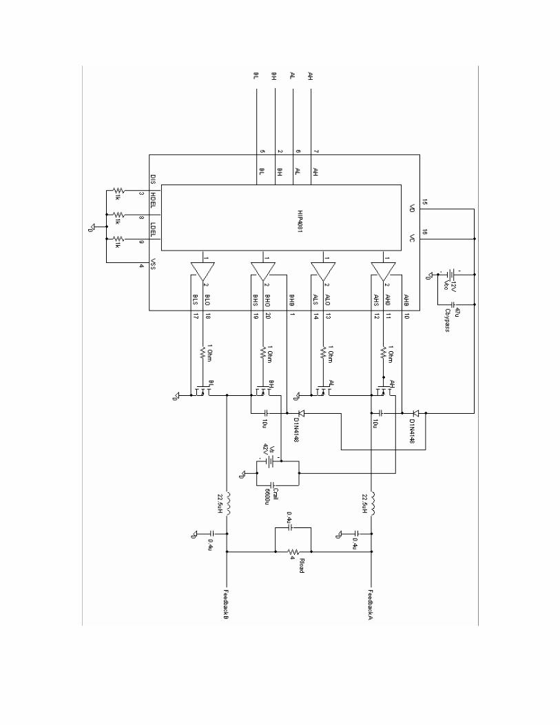

LM111/LM211/LM311Voltage Comparator1.0 General DescriptionThe LM111, LM211 and LM311 are voltage comparators thathave input currents nearly a thousand times lower thandevices like the LM106 or LM710. They are also designed tooperate over a wider range of supply voltages: from standard±15V op amp supplies down to the single 5V supply used forIC logic. Their output is compatible with RTL, DTL and TTLas well as MOS circuits. Further, they can drive lamps orrelays, switching voltages up to 50V at currents as high as50 mA.
Both the inputs and the outputs of the LM111, LM211 or theLM311 can be isolated from system ground, and the outputcan drive loads referred to ground, the positive supply or thenegative supply. Offset balancing and strobe capability areprovided and outputs can be wire OR’ed. Although slowerthan the LM106 and LM710 (200 ns response time vs 40 ns)
the devices are also much less prone to spurious oscilla-tions. The LM111 has the same pin configuration as theLM106 and LM710.
The LM211 is identical to the LM111, except that its perfor-mance is specified over a −25˚C to +85˚C temperature rangeinstead of −55˚C to +125˚C. The LM311 has a temperaturerange of 0˚C to +70˚C.
2.0 Featuresn Operates from single 5V supplyn Input current: 150 nA max. over temperaturen Offset current: 20 nA max. over temperaturen Differential input voltage range: ±30Vn Power consumption: 135 mW at ±15V
3.0 Typical Applications (Note 3)
Offset Balancing
DS005704-36
Strobing
DS005704-37
Note: Do Not Ground Strobe Pin. Output is turned off when current ispulled from Strobe Pin.
Increasing Input Stage Current (Note 1)
DS005704-38
Note 1: Increases typical common mode slew from 7.0V/µs to 18V/µs.
Detector for Magnetic Transducer
DS005704-39
January 2001LM
111/LM211/LM
311Voltage
Com
parator
© 2001 National Semiconductor Corporation DS005704 www.national.com
3.0 Typical Applications (Note 3) (Continued)
Digital Transmission Isolator
DS005704-40
Relay Driver with Strobe
DS005704-41
*Absorbs inductive kickback of relay and protects IC from severe voltagetransients on V++ line.Note: Do Not Ground Strobe Pin.
Strobing off Both Input and Output Stages (Note 2)
DS005704-42
Note: Do Not Ground Strobe Pin.
Note 2: Typical input current is 50 pA with inputs strobed off.
Note 3: Pin connections shown on schematic diagram and typical applications are for H08 metal can package.
Positive Peak Detector
DS005704-23
*Solid tantalum
Zero Crossing Detector Driving MOS Logic
DS005704-24
LM11
1/LM
211/
LM31
1
www.national.com 2

4.0 Absolute Maximum Ratings forthe LM111/LM211 (Note 10)
If Military/Aerospace specified devices are required,please contact the National Semiconductor Sales Office/Distributors for availability and specifications.
Total Supply Voltage (V84) 36VOutput to Negative Supply Voltage (V74) 50VGround to Negative Supply Voltage (V14) 30VDifferential Input Voltage ±30VInput Voltage (Note 4) ±15VOutput Short Circuit Duration 10 sec
Operating Temperature RangeLM111 −55˚C to 125˚CLM211 −25˚C to 85˚C
Lead Temperature (Soldering, 10 sec) 260˚CVoltage at Strobe Pin V+−5VSoldering Information
Dual-In-Line PackageSoldering (10 seconds) 260˚C
Small Outline PackageVapor Phase (60 seconds) 215˚CInfrared (15 seconds) 220˚C
See AN-450 “Surface Mounting Methods and Their Effecton Product Reliability” for other methods of solderingsurface mount devices.
ESD Rating (Note 11) 300V
Electrical Characteristics (Note 6)for the LM111 and LM211
Parameter Conditions Min Typ Max Units
Input Offset Voltage (Note 7) TA=25˚C, RS≤50k 0.7 3.0 mV
Input Offset Current TA=25˚C 4.0 10 nA
Input Bias Current TA=25˚C 60 100 nA
Voltage Gain TA=25˚C 40 200 V/mV
Response Time (Note 8) TA=25˚C 200 ns
Saturation Voltage VIN≤−5 mV, IOUT=50 mA 0.75 1.5 V
TA=25˚C
Strobe ON Current (Note 9) TA=25˚C 2.0 5.0 mA
Output Leakage Current VIN≥5 mV, VOUT=35V 0.2 10 nA
TA=25˚C, ISTROBE=3 mA
Input Offset Voltage (Note 7) RS≤50 k 4.0 mV
Input Offset Current (Note 7) 20 nA
Input Bias Current 150 nA
Input Voltage Range V+=15V, V−=−15V, Pin 7 −14.5 13.8,-14.7 13.0 V
Pull-Up May Go To 5V
Saturation Voltage V+≥4.5V, V−=0 0.23 0.4 V
VIN≤−6 mV, IOUT≤8 mA
Output Leakage Current VIN≥5 mV, VOUT=35V 0.1 0.5 µA
Positive Supply Current TA=25˚C 5.1 6.0 mA
Negative Supply Current TA=25˚C 4.1 5.0 mA
Note 4: This rating applies for ±15 supplies. The positive input voltage limit is 30V above the negative supply. The negative input voltage limit is equal to thenegative supply voltage or 30V below the positive supply, whichever is less.
Note 5: The maximum junction temperature of the LM111 is 150˚C, while that of the LM211 is 110˚C. For operating at elevated temperatures, devices in the H08package must be derated based on a thermal resistance of 165˚C/W, junction to ambient, or 20˚C/W, junction to case. The thermal resistance of the dual-in-linepackage is 110˚C/W, junction to ambient.
Note 6: These specifications apply for VS=±15V and Ground pin at ground, and −55˚C≤TA≤+125˚C, unless otherwise stated. With the LM211, however, alltemperature specifications are limited to −25˚C≤TA≤+85˚C. The offset voltage, offset current and bias current specifications apply for any supply voltage from a single5V supply up to ±15V supplies.
Note 7: The offset voltages and offset currents given are the maximum values required to drive the output within a volt of either supply with a 1 mA load. Thus, theseparameters define an error band and take into account the worst-case effects of voltage gain and RS.
Note 8: The response time specified (see definitions) is for a 100 mV input step with 5 mV overdrive.
Note 9: This specification gives the range of current which must be drawn from the strobe pin to ensure the output is properly disabled. Do not short the strobe pinto ground; it should be current driven at 3 to 5 mA.
Note 10: Refer to RETS111X for the LM111H, LM111J and LM111J-8 military specifications.
Note 11: Human body model, 1.5 kΩ in series with 100 pF.
LM111/LM
211/LM311
www.national.com3
5.0 Absolute Maximum Ratings forthe LM311 (Note 12)
If Military/Aerospace specified devices are required,please contact the National Semiconductor Sales Office/Distributors for availability and specifications.
Total Supply Voltage (V84) 36VOutput to Negative Supply Voltage (V74) 40VGround to Negative Supply Voltage (V14) 30VDifferential Input Voltage ±30VInput Voltage (Note 13) ±15VPower Dissipation (Note 14) 500 mWESD Rating (Note 19) 300VOutput Short Circuit Duration 10 sec
Operating Temperature Range 0˚ to 70˚CStorage Temperature Range −65˚C to 150˚CLead Temperature (soldering, 10 sec) 260˚CVoltage at Strobe Pin V+−5VSoldering Information
Dual-In-Line PackageSoldering (10 seconds) 260˚C
Small Outline PackageVapor Phase (60 seconds) 215˚CInfrared (15 seconds) 220˚C
See AN-450 “Surface Mounting Methods and Their Effecton Product Reliability” for other methods of solderingsurface mount devices.
Electrical Characteristics (Note 15)for the LM311
Parameter Conditions Min Typ Max Units
Input Offset Voltage (Note 16) TA=25˚C, RS≤50k 2.0 7.5 mV
Input Offset Current(Note 16) TA=25˚C 6.0 50 nA
Input Bias Current TA=25˚C 100 250 nA
Voltage Gain TA=25˚C 40 200 V/mV
Response Time (Note 17) TA=25˚C 200 ns
Saturation Voltage VIN≤−10 mV, IOUT=50 mA 0.75 1.5 V
TA=25˚C
Strobe ON Current (Note 18) TA=25˚C 2.0 5.0 mA
Output Leakage Current VIN≥10 mV, VOUT=35V
TA=25˚C, ISTROBE=3 mA 0.2 50 nA
V− = Pin 1 = −5V
Input Offset Voltage (Note 16) RS≤50K 10 mV
Input Offset Current (Note 16) 70 nA
Input Bias Current 300 nA
Input Voltage Range −14.5 13.8,−14.7 13.0 V
Saturation Voltage V+≥4.5V, V−=0 0.23 0.4 V
VIN≤−10 mV, IOUT≤8 mA
Positive Supply Current TA=25˚C 5.1 7.5 mA
Negative Supply Current TA=25˚C 4.1 5.0 mA
Note 12: “Absolute Maximum Ratings indicate limits beyond which damage to the device may occur. Operating Ratings indicate conditions for which the device isfunctional, but do not guarantee specific performance limits.”
Note 13: This rating applies for ±15V supplies. The positive input voltage limit is 30V above the negative supply. The negative input voltage limit is equal to thenegative supply voltage or 30V below the positive supply, whichever is less.
Note 14: The maximum junction temperature of the LM311 is 110˚C. For operating at elevated temperature, devices in the H08 package must be derated basedon a thermal resistance of 165˚C/W, junction to ambient, or 20˚C/W, junction to case. The thermal resistance of the dual-in-line package is 100˚C/W, junction toambient.
Note 15: These specifications apply for VS=±15V and Pin 1 at ground, and 0˚C < TA < +70˚C, unless otherwise specified. The offset voltage, offset current andbias current specifications apply for any supply voltage from a single 5V supply up to ±15V supplies.
Note 16: The offset voltages and offset currents given are the maximum values required to drive the output within a volt of either supply with 1 mA load. Thus, theseparameters define an error band and take into account the worst-case effects of voltage gain and RS.
Note 17: The response time specified (see definitions) is for a 100 mV input step with 5 mV overdrive.
Note 18: This specification gives the range of current which must be drawn from the strobe pin to ensure the output is properly disabled. Do not short the strobepin to ground; it should be current driven at 3 to 5 mA.
Note 19: Human body model, 1.5 kΩ in series with 100 pF.
LM11
1/LM
211/
LM31
1
www.national.com 4
6.0 LM111/LM211 Typical Performance Characteristics
Input Bias Current
DS005704-43
Input Bias Current
DS005704-44
Input Bias Current
DS005704-45
Input Bias Current
DS005704-46
Input Bias Current
DS005704-47
Input Bias Current
DS005704-48
LM111/LM
211/LM311
www.national.com5

6.0 LM111/LM211 Typical Performance Characteristics (Continued)
Input Bias CurrentInput Overdrives
DS005704-49
Input Bias CurrentInput Overdrives
DS005704-50
Input Bias Current
DS005704-51
Response Time for VariousInput Overdrives
DS005704-52
Response Time for VariousInput Overdrives
DS005704-53
Output Limiting Characteristics
DS005704-54
LM11
1/LM
211/
LM31
1
www.national.com 6
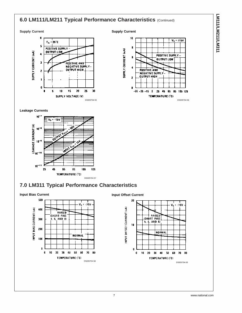
6.0 LM111/LM211 Typical Performance Characteristics (Continued)
7.0 LM311 Typical Performance Characteristics
Supply Current
DS005704-55
Supply Current
DS005704-56
Leakage Currents
DS005704-57
Input Bias Current
DS005704-58
Input Offset Current
DS005704-59
LM111/LM
211/LM311
www.national.com7

7.0 LM311 Typical Performance Characteristics (Continued)
Offset Error
DS005704-60
Input Characteristics
DS005704-61
Common Mode Limits
DS005704-62
Transfer Function
DS005704-63
Response Time for VariousInput Overdrives
DS005704-64
Response Time for VariousInput Overdrives
DS005704-65
LM11
1/LM
211/
LM31
1
www.national.com 8

7.0 LM311 Typical Performance Characteristics (Continued)
Output Saturation Voltage
DS005704-66
Response Time for VariousInput Overdrives
DS005704-67
Response Time for VariousInput Overdrives
DS005704-68
Output Limiting Characteristics
DS005704-69
Supply Current
DS005704-70
Supply Current
DS005704-71
LM111/LM
211/LM311
www.national.com9

7.0 LM311 Typical Performance Characteristics (Continued)
8.0 Application Hints
8.1 CIRCUIT TECHNIQUES FOR AVOIDINGOSCILLATIONS IN COMPARATOR APPLICATIONS
When a high-speed comparator such as the LM111 is usedwith fast input signals and low source impedances, the out-put response will normally be fast and stable, assuming thatthe power supplies have been bypassed (with 0.1 µF disccapacitors), and that the output signal is routed well awayfrom the inputs (pins 2 and 3) and also away from pins 5 and6.
However, when the input signal is a voltage ramp or a slowsine wave, or if the signal source impedance is high (1 kΩ to100 kΩ), the comparator may burst into oscillation near thecrossing-point. This is due to the high gain and wide band-width of comparators like the LM111. To avoid oscillation orinstability in such a usage, several precautions are recom-mended, as shown in Figure 1 below.
1. The trim pins (pins 5 and 6) act as unwanted auxiliaryinputs. If these pins are not connected to a trim-pot, theyshould be shorted together. If they are connected to atrim-pot, a 0.01 µF capacitor C1 between pins 5 and 6will minimize the susceptibility to AC coupling. A smallercapacitor is used if pin 5 is used for positive feedback asin Figure 1.
2. Certain sources will produce a cleaner comparator out-put waveform if a 100 pF to 1000 pF capacitor C2 isconnected directly across the input pins.
3. When the signal source is applied through a resistivenetwork, RS, it is usually advantageous to choose an RS'of substantially the same value, both for DC and fordynamic (AC) considerations. Carbon, tin-oxide, andmetal-film resistors have all been used successfully incomparator input circuitry. Inductive wirewound resistorsare not suitable.
4. When comparator circuits use input resistors (eg. sum-ming resistors), their value and placement are particu-larly important. In all cases the body of the resistorshould be close to the device or socket. In other wordsthere should be very little lead length or printed-circuitfoil run between comparator and resistor to radiate orpick up signals. The same applies to capacitors, pots,etc. For example, if RS=10 kΩ, as little as 5 inches oflead between the resistors and the input pins can result
in oscillations that are very hard to damp. Twisting theseinput leads tightly is the only (second best) alternative toplacing resistors close to the comparator.
5. Since feedback to almost any pin of a comparator canresult in oscillation, the printed-circuit layout should beengineered thoughtfully. Preferably there should be agroundplane under the LM111 circuitry, for example, oneside of a double-layer circuit card. Ground foil (or, posi-tive supply or negative supply foil) should extend be-tween the output and the inputs, to act as a guard. Thefoil connections for the inputs should be as small andcompact as possible, and should be essentially sur-rounded by ground foil on all sides, to guard againstcapacitive coupling from any high-level signals (such asthe output). If pins 5 and 6 are not used, they should beshorted together. If they are connected to a trim-pot, thetrim-pot should be located, at most, a few inches awayfrom the LM111, and the 0.01 µF capacitor should beinstalled. If this capacitor cannot be used, a shieldingprinted-circuit foil may be advisable between pins 6 and7. The power supply bypass capacitors should be lo-cated within a couple inches of the LM111. (Some othercomparators require the power-supply bypass to be lo-cated immediately adjacent to the comparator.)
6. It is a standard procedure to use hysteresis (positivefeedback) around a comparator, to prevent oscillation,and to avoid excessive noise on the output because thecomparator is a good amplifier for its own noise. In thecircuit of Figure 2, the feedback from the output to thepositive input will cause about 3 mV of hysteresis. How-ever, if RS is larger than 100Ω, such as 50 kΩ, it wouldnot be reasonable to simply increase the value of thepositive feedback resistor above 510 kΩ. The circuit ofFigure 3 could be used, but it is rather awkward. See thenotes in paragraph 7 below.
Leakage Currents
DS005704-72
LM11
1/LM
211/
LM31
1
www.national.com 10

8.0 Application Hints (Continued)
7. When both inputs of the LM111 are connected to activesignals, or if a high-impedance signal is driving thepositive input of the LM111 so that positive feedbackwould be disruptive, the circuit of Figure 1 is ideal. Thepositive feedback is to pin 5 (one of the offset adjust-ment pins). It is sufficient to cause 1 to 2 mV hysteresisand sharp transitions with input triangle waves from afew Hz to hundreds of kHz. The positive-feedback signalacross the 82Ω resistor swings 240 mV below the posi-
tive supply. This signal is centered around the nominalvoltage at pin 5, so this feedback does not add to theVOS of the comparator. As much as 8 mV of VOS can betrimmed out, using the 5 kΩ pot and 3 kΩ resistor asshown.
8. These application notes apply specifically to the LM111,LM211, LM311, and LF111 families of comparators, andare applicable to all high-speed comparators in general,(with the exception that not all comparators have trimpins).
DS005704-29
Pin connections shown are for LM111H in the H08 hermetic package
FIGURE 1. Improved Positive Feedback
DS005704-30
Pin connections shown are for LM111H in the H08 hermetic package
FIGURE 2. Conventional Positive Feedback
LM111/LM
211/LM311
www.national.com11

8.0 Application Hints (Continued)
9.0 Typical Applications (Pin numbers refer to H08 package)
DS005704-31
FIGURE 3. Positive Feedback with High Source Resistance
Zero Crossing Detector Driving MOS Switch
DS005704-13
100 kHz Free Running Multivibrator
DS005704-14
*TTL or DTL fanout of two
LM11
1/LM
211/
LM31
1
www.national.com 12

9.0 Typical Applications (Pin numbers refer to H08 package) (Continued)
10 Hz to 10 kHz Voltage Controlled Oscillator
DS005704-15
*Adjust for symmetrical square wave time when VIN = 5 mV†Minimum capacitance 20 pF Maximum frequency 50 kHz
Driving Ground-Referred Load
DS005704-16
*Input polarity is reversed when using pin 1 as output.
Using Clamp Diodes to Improve Response
DS005704-17
TTL Interface with High Level Logic
DS005704-18
*Values shown are for a 0 to 30V logic swing and a 15V threshold.†May be added to control speed and reduce susceptibility to noise spikes.
LM111/LM
211/LM311
www.national.com13

9.0 Typical Applications (Pin numbers refer to H08 package) (Continued)
Crystal Oscillator
DS005704-19
Comparator and Solenoid Driver
DS005704-20
Precision Squarer
DS005704-21
*Solid tantalum†Adjust to set clamp level
LM11
1/LM
211/
LM31
1
www.national.com 14
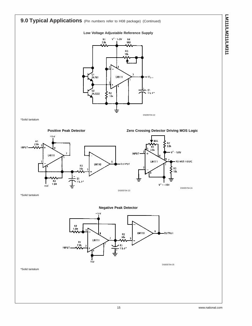
9.0 Typical Applications (Pin numbers refer to H08 package) (Continued)
Low Voltage Adjustable Reference Supply
DS005704-22
*Solid tantalum
Positive Peak Detector
DS005704-23
*Solid tantalum
Zero Crossing Detector Driving MOS Logic
DS005704-24
Negative Peak Detector
DS005704-25
*Solid tantalum
LM111/LM
211/LM311
www.national.com15

9.0 Typical Applications (Pin numbers refer to H08 package) (Continued)
Precision Photodiode Comparator
DS005704-26
*R2 sets the comparison level. At comparison, the photodiode has less than 5 mV across it, decreasing leakages by an order of magnitude.
Switching Power Amplifier
DS005704-27
LM11
1/LM
211/
LM31
1
www.national.com 16

9.0 Typical Applications (Pin numbers refer to H08 package) (Continued)
Switching Power Amplifier
DS005704-28
LM111/LM
211/LM311
www.national.com17

10.0 Schematic Diagram (Note 20)
DS005704-5
Note 20: Pin connections shown on schematic diagram are for H08 package.
LM11
1/LM
211/
LM31
1
www.national.com 18

11.0 Connection Diagrams
Note 21: Also available per JM38510/10304
Metal Can Package
DS005704-6
Note: Pin 4 connected to case
Top ViewOrder Number LM111H, LM111H/883 (Note 21) , LM211H or LM311H
See NS Package Number H08C
Dual-In-Line Package
DS005704-34
Top ViewOrder Number LM111J-8, LM111J-8/883 (Note 21),
LM311M, LM311MX or LM311NSee NS Package Number J08A, M08A or N08E
Dual-In-Line Package
DS005704-35
Top ViewOrder Number LM111J/883 (Note 21)
See NS Package Number J14A or N14A
DS005704-33
Order Number LM111W/883 (Note 21), LM111WG/883See NS Package Number W10A, WG10A
LM111/LM
211/LM311
www.national.com19

12.0 Physical Dimensions inches (millimeters) unless otherwise noted
Metal Can Package (H)Order Number LM111H, LM111H/883, LM211H or LM311H
NS Package Number H08C
Cavity Dual-In-Line Package (J)Order Number LM111J-8, LM111J-8/883
NS Package Number J08A
LM11
1/LM
211/
LM31
1
www.national.com 20
12.0 Physical Dimensions inches (millimeters) unless otherwise noted (Continued)
Dual-In-Line Package (J)Order Number LM111J/883NS Package Number J14A
Dual-In-Line Package (M)Order Number LM311M, LM311MX
NS Package Number M08A
LM111/LM
211/LM311
www.national.com21
12.0 Physical Dimensions inches (millimeters) unless otherwise noted (Continued)
Dual-In-Line Package (N)Order Number LM311N
NS Package Number N08E
Order Number LM111W/883, LM111WG/883NS Package Number W10A, WG10A
LM11
1/LM
211/
LM31
1
www.national.com 22

Notes
LIFE SUPPORT POLICY
NATIONAL’S PRODUCTS ARE NOT AUTHORIZED FOR USE AS CRITICAL COMPONENTS IN LIFE SUPPORTDEVICES OR SYSTEMS WITHOUT THE EXPRESS WRITTEN APPROVAL OF THE PRESIDENT AND GENERALCOUNSEL OF NATIONAL SEMICONDUCTOR CORPORATION. As used herein:
1. Life support devices or systems are devices orsystems which, (a) are intended for surgical implantinto the body, or (b) support or sustain life, andwhose failure to perform when properly used inaccordance with instructions for use provided in thelabeling, can be reasonably expected to result in asignificant injury to the user.
2. A critical component is any component of a lifesupport device or system whose failure to performcan be reasonably expected to cause the failure ofthe life support device or system, or to affect itssafety or effectiveness.
National SemiconductorCorporationAmericasTel: 1-800-272-9959Fax: 1-800-737-7018Email: [email protected]
National SemiconductorEurope
Fax: +49 (0) 180-530 85 86Email: [email protected]
Deutsch Tel: +49 (0) 69 9508 6208English Tel: +44 (0) 870 24 0 2171Français Tel: +33 (0) 1 41 91 8790
National SemiconductorAsia Pacific CustomerResponse GroupTel: 65-2544466Fax: 65-2504466Email: [email protected]
National SemiconductorJapan Ltd.Tel: 81-3-5639-7560Fax: 81-3-5639-7507
www.national.com
LM111/LM
211/LM311
VoltageC
omparator
National does not assume any responsibility for use of any circuitry described, no circuit patent licenses are implied and National reserves the right at any time without notice to change said circuitry and specifications.


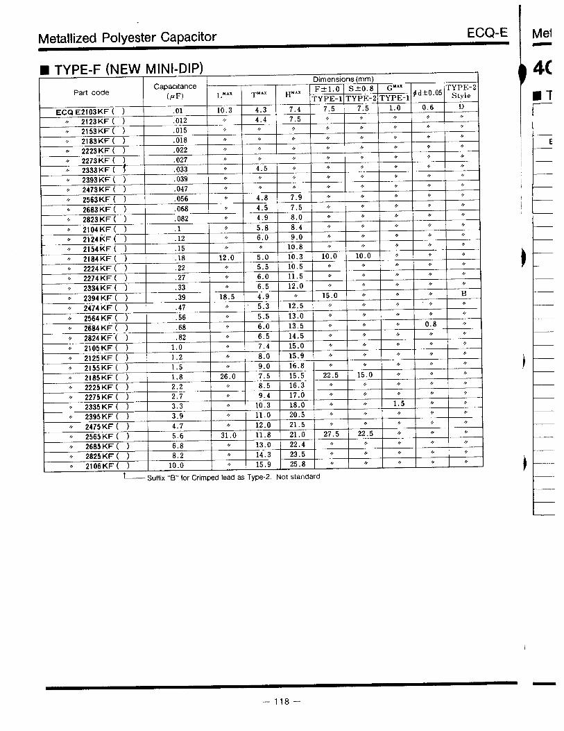


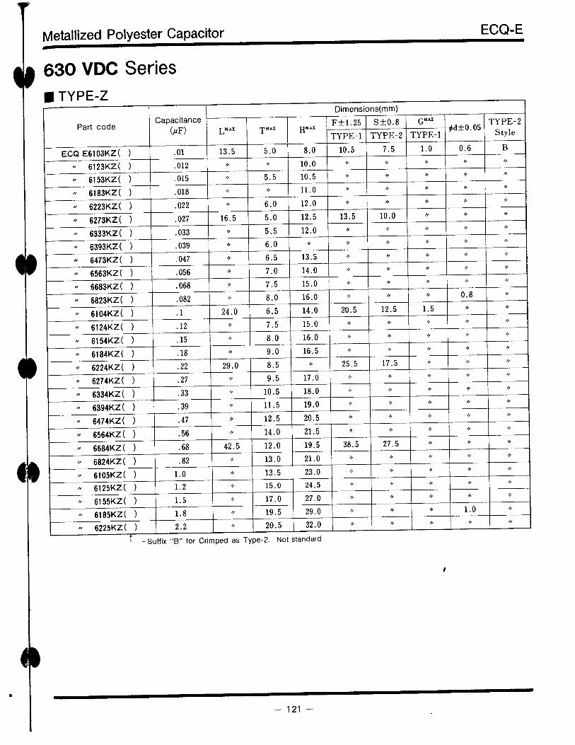
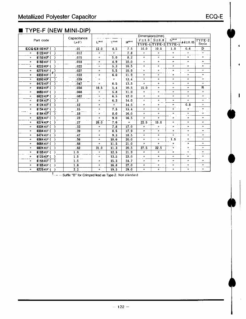

©
August 2002
FD
P038A
N06A
0 / FD
I038AN
06A0
FDP038AN06A0 / FDI038AN06A0N-Channel PowerTrench® MOSFET60V, 80A, 3.8mΩFeatures
• rDS(ON) = 3.5mΩ (Typ.), VGS = 10V, ID = 80A
• Qg(tot) = 95nC (Typ.), VGS = 10V
• Low Miller Charge
• Low QRR Body Diode
• UIS Capability (Single Pulse and Repetitive Pulse)
• Qualified to AEC Q101
Formerly developmental type 82584
Applications
• Motor / Body Load Control
• ABS Systems
• Powertrain Management
• Injection Systems
• DC-DC converters and Off-line UPS
• Distributed Power Architectures and VRMs
• Primary Switch for 12V and 24V systems
D
G
SDRAIN (FLANGE)
DRAINSOURCE
GATE
TO-262ABFDI SERIES
TO-220ABFDP SERIES
DRAIN
DRAIN
GATE
SOURCE(FLANGE)
MOSFET Maximum Ratings TC = 25°C unless otherwise noted
Thermal Characteristics
This product has been designed to meet the extreme test conditions and environment demanded by the automotive industry. For a copy of the requirements, see AEC Q101 at: http://www.aecouncil.com/
Reliability data can be found at: http://www.fairchildsemi.com/products/discrete/reliability/index.html.All Fairchild Semiconductor products are manufactured, assembled and tested under ISO9000 and QS9000 quality
systems certification.
Symbol Parameter Ratings UnitsVDSS Drain to Source Voltage 60 V
VGS Gate to Source Voltage ±20 V
ID
Drain Current80 AContinuous (TC < 151oC, VGS = 10V)
Continuous (Tamb = 25oC, VGS = 10V, with RθJA = 62oC/W) 17 A
Pulsed Figure 4 A
EAS Single Pulse Avalanche Energy (Note 1) 625 mJ
PDPower dissipation 310 W
Derate above 25oC 2.07 W/oC
TJ, TSTG Operating and Storage Temperature -55 to 175 oC
RθJC Thermal Resistance Junction to Case TO-220, TO-262 0.48 oC/W
RθJA Thermal Resistance Junction to Ambient TO-220, TO-262 (Note 2) 62 oC/W
2002 Fairchild Semiconductor Corporation FDP038AN06A0 / FDI038AN06A0 Rev. A1
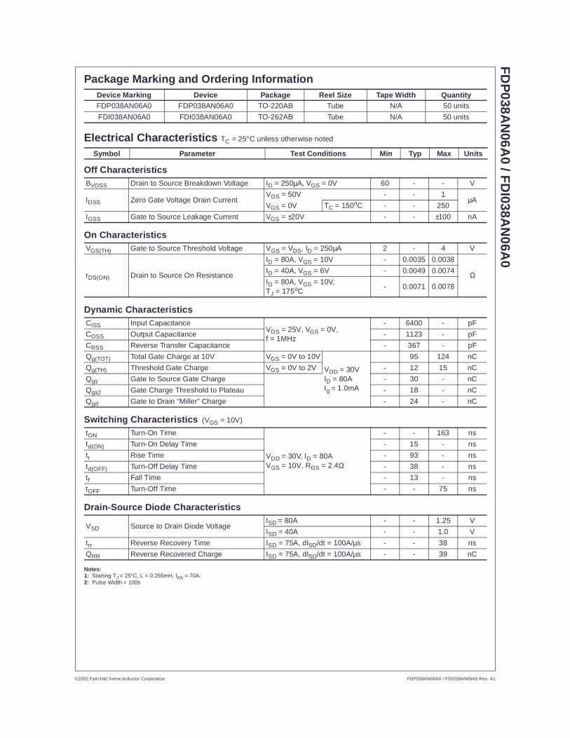
©
FD
P038A
N06A
0 / FD
I038AN
06A0
Package Marking and Ordering Information
Electrical Characteristics TC = 25°C unless otherwise noted
Off Characteristics
On Characteristics
Dynamic Characteristics
Switching Characteristics (VGS = 10V)
Drain-Source Diode Characteristics
Notes: 1: Starting TJ = 25°C, L = 0.255mH, IAS = 70A.2: Pulse Width = 100s
Device Marking Device Package Reel Size Tape Width QuantityFDP038AN06A0 FDP038AN06A0 TO-220AB Tube N/A 50 units
FDI038AN06A0 FDI038AN06A0 TO-262AB Tube N/A 50 units
Symbol Parameter Test Conditions Min Typ Max Units
BVDSS Drain to Source Breakdown Voltage ID = 250µA, VGS = 0V 60 - - V
IDSS Zero Gate Voltage Drain CurrentVDS = 50V - - 1
µAVGS = 0V TC = 150oC - - 250
IGSS Gate to Source Leakage Current VGS = ±20V - - ±100 nA
VGS(TH) Gate to Source Threshold Voltage VGS = VDS, ID = 250µA 2 - 4 V
rDS(ON) Drain to Source On Resistance
ID = 80A, VGS = 10V - 0.0035 0.0038
ΩID = 40A, VGS = 6V - 0.0049 0.0074
ID = 80A, VGS = 10V, TJ = 175oC
- 0.0071 0.0078
CISS Input CapacitanceVDS = 25V, VGS = 0V,f = 1MHz
- 6400 - pF
COSS Output Capacitance - 1123 - pF
CRSS Reverse Transfer Capacitance - 367 - pF
Qg(TOT) Total Gate Charge at 10V VGS = 0V to 10V
VDD = 30VID = 80AIg = 1.0mA
95 124 nC
Qg(TH) Threshold Gate Charge VGS = 0V to 2V - 12 15 nC
Qgs Gate to Source Gate Charge - 30 - nC
Qgs2 Gate Charge Threshold to Plateau - 18 - nC
Qgd Gate to Drain “Miller” Charge - 24 - nC
tON Turn-On Time
VDD = 30V, ID = 80AVGS = 10V, RGS = 2.4Ω
- - 163 ns
td(ON) Turn-On Delay Time - 15 - ns
tr Rise Time - 93 - ns
td(OFF) Turn-Off Delay Time - 38 - ns
tf Fall Time - 13 - ns
tOFF Turn-Off Time - - 75 ns
VSD Source to Drain Diode VoltageISD = 80A - - 1.25 V
ISD = 40A - - 1.0 V
trr Reverse Recovery Time ISD = 75A, dISD/dt = 100A/µs - - 38 ns
QRR Reverse Recovered Charge ISD = 75A, dISD/dt = 100A/µs - - 39 nC
2002 Fairchild Semiconductor Corporation FDP038AN06A0 / FDI038AN06A0 Rev. A1

©
FD
P038A
N06A
0 / FD
I038AN
06A0
Typical Characteristics TC = 25°C unless otherwise noted
Figure 1. Normalized Power Dissipation vs Ambient Temperature
Figure 2. Maximum Continuous Drain Current vs Case Temperature
Figure 3. Normalized Maximum Transient Thermal Impedance
Figure 4. Peak Current Capability
TC, CASE TEMPERATURE (oC)
PO
WE
R D
ISS
IPA
TIO
N M
ULT
IPL
IER
00 25 50 75 100 175
0.2
0.4
0.6
0.8
1.0
1.2
125 1500
50
100
150
200
250
25 50 75 100 125 150 175
I D, D
RA
IN C
UR
RE
NT
(A
)
TC, CASE TEMPERATURE (oC)
CURRENT LIMITEDBY PACKAGE
0.1
1
10-5 10-4 10-3 10-2 10-1 100 1010.01
2
t, RECTANGULAR PULSE DURATION (s)
ZθJ
C, N
OR
MA
LIZ
ED
TH
ER
MA
L IM
PE
DA
NC
E
NOTES:DUTY FACTOR: D = t1/t2PEAK TJ = PDM x ZθJC x RθJC + TC
PDM
t1t2
0.50.20.10.05
0.010.02
DUTY CYCLE - DESCENDING ORDER
SINGLE PULSE
I DM
, PE
AK
CU
RR
EN
T (
A)
t , PULSE WIDTH (s)
10-5 10-4 10-3 10-2 10-1 100 101
TC = 25oC
I = I25 175 - TC
150
FOR TEMPERATURES
ABOVE 25oC DERATE PEAK
CURRENT AS FOLLOWS:
TRANSCONDUCTANCEMAY LIMIT CURRENTIN THIS REGION
VGS = 10V
10
100
1000
3000
2002 Fairchild Semiconductor Corporation FDP038AN06A0 / FDI038AN06A0 Rev. A1

©
FD
P038A
N06A
0 / FD
I038AN
06A0
Figure 5. Forward Bias Safe Operating Area NOTE: Refer to Fairchild Application Notes AN7514 and AN7515Figure 6. Unclamped Inductive Switching Capability
Figure 7. Transfer Characteristics Figure 8. Saturation Characteristics
Figure 9. Drain to Source On Resistance vs Drain Current
Figure 10. Normalized Drain to Source On Resistance vs Junction Temperature
Typical Characteristics TC = 25°C unless otherwise noted
0.1
1
10
100
1000
1 10 100
2000
VDS, DRAIN TO SOURCE VOLTAGE (V)
I D, D
RA
IN C
UR
RE
NT
(A
)
TJ = MAX RATEDTC = 25oC
SINGLE PULSE
LIMITED BY rDS(ON)
AREA MAY BEOPERATION IN THIS
10µs
1ms
DC
100µs
10ms
1
10
100
0.01 0.1 1 10 100
I AS
, AVA
LA
NC
HE
CU
RR
EN
T (
A)
tAV, TIME IN AVALANCHE (ms)
STARTING TJ = 25oC
STARTING TJ = 150oC
tAV = (L)(IAS)/(1.3*RATED BVDSS - VDD)If R = 0
If R ≠ 0tAV = (L/R)ln[(IAS*R)/(1.3*RATED BVDSS - VDD) +1]
0
40
80
120
160
3.0 3.5 4.0 4.5 5.0 5.5 6
I D, D
RA
IN C
UR
RE
NT
(A
)
VGS, GATE TO SOURCE VOLTAGE (V)
PULSE DURATION = 80µsDUTY CYCLE = 0.5% MAXVDD = 15V
TJ = 25oC
TJ = -55oC
TJ = 175oC
0
40
80
120
160
0 0.5 1.0 1.5
I D, D
RA
IN C
UR
RE
NT
(A
)
VDS, DRAIN TO SOURCE VOLTAGE (V)
PULSE DURATION = 80µsDUTY CYCLE = 0.5% MAX
VGS = 5V
TC = 25oC
VGS = 20V VGS = 10V
VGS = 6V
3
4
5
0 20 40 60 80
6
ID, DRAIN CURRENT (A)
DR
AIN
TO
SO
UR
CE
ON
RE
SIS
TAN
CE
(mΩ)
VGS = 6V
VGS = 10V
PULSE DURATION = 80µsDUTY CYCLE = 0.5% MAX
0.5
1.0
1.5
2.0
2.5
NO
RM
AL
IZE
D D
RA
IN T
O S
OU
RC
E
TJ, JUNCTION TEMPERATURE (oC)
ON
RE
SIS
TAN
CE
VGS = 10V, ID =80A
PULSE DURATION = 80µsDUTY CYCLE = 0.5% MAX
-80 -40 0 40 80 120 160 200
2002 Fairchild Semiconductor Corporation FDP038AN06A0 / FDI038AN06A0 Rev. A1
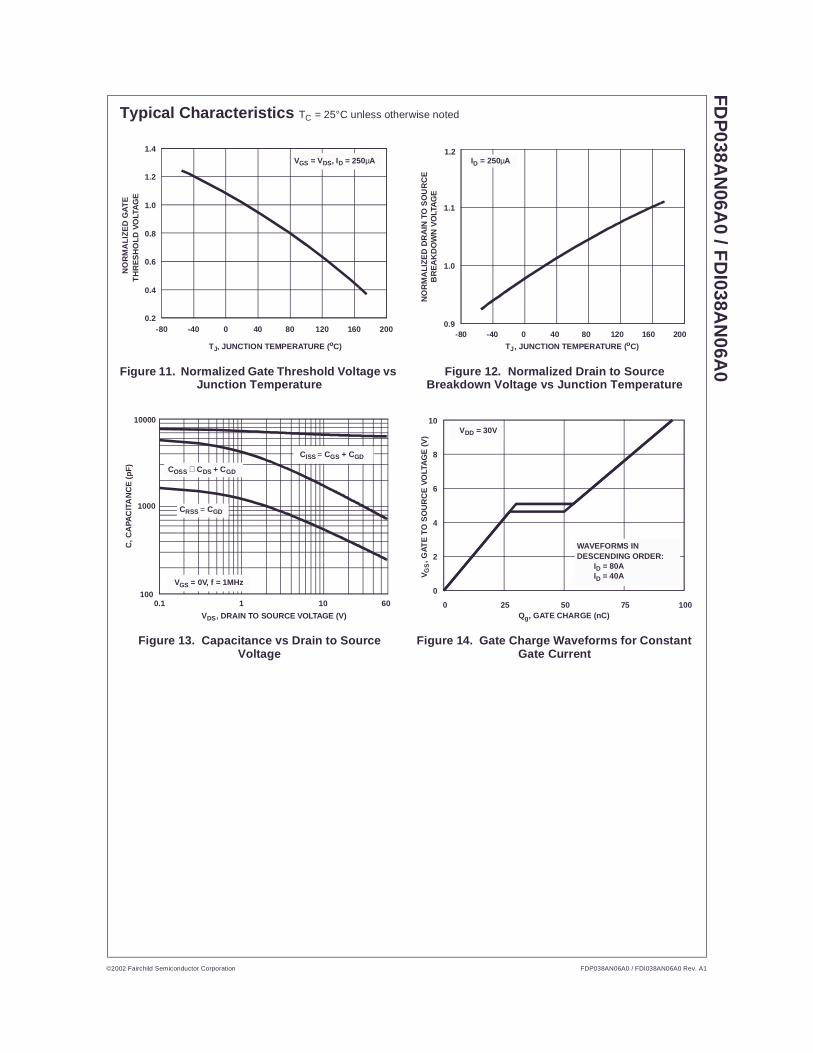
©
FD
P038A
N06A
0 / FD
I038AN
06A0
Figure 11. Normalized Gate Threshold Voltage vsJunction TemperatureFigure 12. Normalized Drain to Source
Breakdown Voltage vs Junction Temperature
Figure 13. Capacitance vs Drain to Source Voltage
Figure 14. Gate Charge Waveforms for Constant Gate Current
Typical Characteristics TC = 25°C unless otherwise noted
0.2
0.4
0.6
0.8
1.0
1.2
1.4VGS = VDS, ID = 250µA
NO
RM
AL
IZE
D G
AT
E
TJ, JUNCTION TEMPERATURE (oC)
TH
RE
SH
OL
D V
OLT
AG
E
-80 -40 0 40 80 120 160 2000.9
1.0
1.1
1.2
TJ, JUNCTION TEMPERATURE (oC)
NO
RM
AL
IZE
D D
RA
IN T
O S
OU
RC
E
ID = 250µA
BR
EA
KD
OW
N V
OLT
AG
E
-80 -40 0 40 80 120 160 200
100
1000
0.1 1 10 60
10000
C, C
APA
CIT
AN
CE
(p
F)
VDS, DRAIN TO SOURCE VOLTAGE (V)
VGS = 0V, f = 1MHz
CISS = CGS + CGD
COSS ≅ CDS + CGD
CRSS = CGD
0
2
4
6
8
10
0 25 50 75 100
VG
S, G
AT
E T
O S
OU
RC
E V
OLT
AG
E (
V)
Qg, GATE CHARGE (nC)
VDD = 30V
ID = 80AID = 40A
WAVEFORMS INDESCENDING ORDER:
2002 Fairchild Semiconductor Corporation FDP038AN06A0 / FDI038AN06A0 Rev. A1
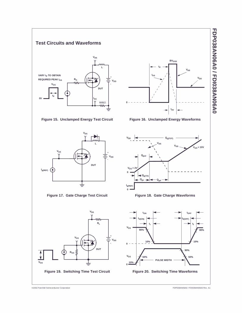
©
FD
P038A
N06A
0 / FD
I038AN
06A0
Test Circuits and Waveforms
Figure 15. Unclamped Energy Test Circuit Figure 16. Unclamped Energy Waveforms
Figure 17. Gate Charge Test Circuit Figure 18. Gate Charge Waveforms
Figure 19. Switching Time Test Circuit Figure 20. Switching Time Waveforms
tP
VGS
0.01Ω
L
IAS
+
-
VDS
VDDRG
DUT
VARY tP TO OBTAIN
REQUIRED PEAK IAS
0V
VDD
VDS
BVDSS
tP
IAS
tAV
0
VGS +
-
VDS
VDD
DUT
Ig(REF)
L
VDD
Qg(TH)
VGS = 2V
Qgs2
Qg(TOT)
VGS = 10V
VDSVGS
Ig(REF)
0
0
Qgs Qgd
VGS
RL
RGS
DUT
+
-VDD
VDS
VGS
tON
td(ON)
tr
90%
10%
VDS90%
10%
tf
td(OFF)
tOFF
90%
50%50%
10%PULSE WIDTH
VGS
0
0
2002 Fairchild Semiconductor Corporation FDP038AN06A0 / FDI038AN06A0 Rev. A1

©
FD
P038A
N06A
0 / FD
I038AN
06A0
PSPICE Electrical Model .SUBCKT FDP038AN06A0 2 1 3 ; rev July 04, 2002Ca 12 8 1.5e-9Cb 15 14 1.5e-9Cin 6 8 6.1e-9
Dbody 7 5 DbodyMODDbreak 5 11 DbreakMODDplcap 10 5 DplcapMOD
Ebreak 11 7 17 18 69.3Eds 14 8 5 8 1Egs 13 8 6 8 1Esg 6 10 6 8 1Evthres 6 21 19 8 1Evtemp 20 6 18 22 1
It 8 17 1
Lgate 1 9 4.81e-9Ldrain 2 5 1.0e-9Lsource 3 7 4.63e-9
RLgate 1 9 48.1RLdrain 2 5 10RLsource 3 7 46.3
Mmed 16 6 8 8 MmedMODMstro 16 6 8 8 MstroMOD Mweak 16 21 8 8 MweakMOD
Rbreak 17 18 RbreakMOD 1Rdrain 50 16 RdrainMOD 1e-4Rgate 9 20 1.36RSLC1 5 51 RSLCMOD 1e-6RSLC2 5 50 1e3Rsource 8 7 RsourceMOD 2.8e-3Rvthres 22 8 RvthresMOD 1Rvtemp 18 19 RvtempMOD 1S1a 6 12 13 8 S1AMODS1b 13 12 13 8 S1BMODS2a 6 15 14 13 S2AMODS2b 13 15 14 13 S2BMOD
Vbat 22 19 DC 1
ESLC 51 50 VALUE=(V(5,51)/ABS(V(5,51)))*(PWR(V(5,51)/(1e-6*250),10))
.MODEL DbodyMOD D (IS=2.4E-11 N=1.04 RS=1.65e-3 TRS1=2.7e-3 TRS2=2e-7+ CJO=4.35e-9 M=5.4e-1 TT=1e-9 XTI=3.9).MODEL DbreakMOD D (RS=1.5e-1 TRS1=1e-3 TRS2=-8.9e-6).MODEL DplcapMOD D (CJO=1.7e-9 IS=1e-30 N=10 M=0.47)
.MODEL MmedMOD NMOS (VTO=3.3 KP=9 IS=1e-30 N=10 TOX=1 L=1u W=1u RG=1.36 T_abs=25)
.MODEL MstroMOD NMOS (VTO=4.00 KP=275 IS=1e-30 N=10 TOX=1 L=1u W=1u T_abs=25)
.MODEL MweakMOD NMOS (VTO=2.72 KP=0.03 IS=1e-30 N=10 TOX=1 L=1u W=1u RG=13.6 RS=0.1 T_abs=25)
.MODEL RbreakMOD RES (TC1=9e-4 TC2=-9e-7)
.MODEL RdrainMOD RES (TC1=4e-2 TC2=3e-4)
.MODEL RSLCMOD RES (TC1=1e-3 TC2=1e-5)
.MODEL RsourceMOD RES (TC1=5e-3 TC2=1e-6)
.MODEL RvthresMOD RES (TC1=-6.7e-3 TC2=-1.5e-5)
.MODEL RvtempMOD RES (TC1=-2.5e-3 TC2=1e-6)
.MODEL S1AMOD VSWITCH (RON=1e-5 ROFF=0.1 VON=-4 VOFF=-1.5)
.MODEL S1BMOD VSWITCH (RON=1e-5 ROFF=0.1 VON=-1.5 VOFF=-4)
.MODEL S2AMOD VSWITCH (RON=1e-5 ROFF=0.1 VON=-1 VOFF=0.5)
.MODEL S2BMOD VSWITCH (RON=1e-5 ROFF=0.1 VON=0.5 VOFF=-1)
.ENDS
Note: For further discussion of the PSPICE model, consult A New PSPICE Sub-Circuit for the Power MOSFET Featuring Global Temperature Options; IEEE Power Electronics Specialist Conference Records, 1991, written by William J. Hepp and C. Frank Wheatley.
1822
+ -
68
+
-
551
+
-
198
+ -
1718
68
+
-
58 +
-
RBREAK
RVTEMP
VBAT
RVTHRES
IT
17 18
19
22
12
13
15S1A
S1B
S2A
S2B
CA CB
EGS EDS
14
8
138
1413
MWEAK
EBREAKDBODY
RSOURCE
SOURCE
11
7 3
LSOURCE
RLSOURCE
CIN
RDRAIN
EVTHRES 1621
8
MMED
MSTRO
DRAIN2
LDRAIN
RLDRAIN
DBREAK
DPLCAP
ESLC
RSLC1
10
5
51
50
RSLC2
1GATE RGATE
EVTEMP
9
ESG
LGATE
RLGATE20
+
-
+
-
+
-
6
2002 Fairchild Semiconductor Corporation FDP038AN06A0 / FDI038AN06A0 Rev. A1
©
FD
P038A
N06A
0 / FD
I038AN
06A0
SABER Electrical Model rev July 4, 2002template FDP038AN06A0 n2,n1,n3 = m_tempelectrical n2,n1,n3number m_temp=25var i iscldp..model dbodymod = (isl=2.4e-11,nl=1.04,rs=1.65e-3,trs1=2.7e-3,trs2=2e-7,cjo=4.35e-9,m=5.4e-1,tt=1e-9,xti=3.9)dp..model dbreakmod = (rs=1.5e-1,trs1=1e-3,trs2=-8.9e-6)dp..model dplcapmod = (cjo=1.7e-9,isl=10e-30,nl=10,m=0.47)m..model mmedmod = (type=_n,vto=3.3,kp=9,is=1e-30, tox=1)m..model mstrongmod = (type=_n,vto=4.00,kp=275,is=1e-30, tox=1)m..model mweakmod = (type=_n,vto=2.72,kp=0.03,is=1e-30, tox=1,rs=0.1) sw_vcsp..model s1amod = (ron=1e-5,roff=0.1,von=-4,voff=-1.5)sw_vcsp..model s1bmod = (ron=1e-5,roff=0.1,von=-1.5,voff=-4)sw_vcsp..model s2amod = (ron=1e-5,roff=0.1,von=-1,voff=0.5)sw_vcsp..model s2bmod = (ron=1e-5,roff=0.1,von=0.5,voff=-1)c.ca n12 n8 = 1.5e-9c.cb n15 n14 = 1.5e-9c.cin n6 n8 = 6.1e-9
dp.dbody n7 n5 = model=dbodymoddp.dbreak n5 n11 = model=dbreakmoddp.dplcap n10 n5 = model=dplcapmod
spe.ebreak n11 n7 n17 n18 = 69.3spe.eds n14 n8 n5 n8 = 1spe.egs n13 n8 n6 n8 = 1spe.esg n6 n10 n6 n8 = 1spe.evthres n6 n21 n19 n8 = 1spe.evtemp n20 n6 n18 n22 = 1
i.it n8 n17 = 1
l.lgate n1 n9 = 4.81e-9l.ldrain n2 n5 = 1.0e-9l.lsource n3 n7 = 4.63e-9
res.rlgate n1 n9 = 48.1res.rldrain n2 n5 = 10res.rlsource n3 n7 = 46.3
m.mmed n16 n6 n8 n8 = model=mmedmod, temp=m_temp, l=1u, w=1um.mstrong n16 n6 n8 n8 = model=mstrongmod, temp=m_temp, l=1u, w=1u m.mweak n16 n21 n8 n8 = model=mweakmod, temp=m_temp, l=1u, w=1u
res.rbreak n17 n18 = 1, tc1=9e-4,tc2=-9e-7res.rdrain n50 n16 = 1e-4, tc1=4e-2,tc2=3e-4res.rgate n9 n20 = 1.36res.rslc1 n5 n51 = 1e-6, tc1=1e-3,tc2=1e-5res.rslc2 n5 n50 = 1e3res.rsource n8 n7 = 2.8e-3, tc1=5e-3,tc2=1e-6res.rvthres n22 n8 = 1, tc1=-6.7e-3,tc2=-1.5e-5res.rvtemp n18 n19 = 1, tc1=-2.5e-3,tc2=1e-6sw_vcsp.s1a n6 n12 n13 n8 = model=s1amodsw_vcsp.s1b n13 n12 n13 n8 = model=s1bmodsw_vcsp.s2a n6 n15 n14 n13 = model=s2amodsw_vcsp.s2b n13 n15 n14 n13 = model=s2bmod
v.vbat n22 n19 = dc=1equations i (n51->n50) +=iscliscl: v(n51,n50) = ((v(n5,n51)/(1e-9+abs(v(n5,n51))))*((abs(v(n5,n51)*1e6/250))** 10))
1822
+ -
68
+
-
198
+ -
1718
68
+
-
58 +
-
RBREAK
RVTEMP
VBAT
RVTHRES
IT
17 18
19
22
12
13
15S1A
S1B
S2A
S2B
CA CB
EGS EDS
14
8
138
1413
MWEAK
EBREAK
DBODY
RSOURCE
SOURCE
11
7 3
LSOURCE
RLSOURCE
CIN
RDRAIN
EVTHRES 1621
8
MMED
MSTRO
DRAIN2
LDRAIN
RLDRAIN
DBREAK
DPLCAP
ISCL
RSLC1
10
5
51
50
RSLC2
1GATE RGATE
EVTEMP
9
ESG
LGATE
RLGATE20
+
-
+
-
+
-
6
2002 Fairchild Semiconductor Corporation FDP038AN06A0 / FDI038AN06A0 Rev. A1

©2002 Fairchild Semiconductor Corporation FDP038AN06A0 / FDI038AN06A0 Rev. A1
FD
P038A
N06A
0 / FD
I038AN
06A0
PSPICE Thermal Model REV 23 July 4, 2002
FDP038AN06A0T
CTHERM1 TH 6 6.45e-3CTHERM2 6 5 3e-2CTHERM3 5 4 1.4e-2CTHERM4 4 3 1.65e-2CTHERM5 3 2 4.85e-2CTHERM6 2 TL 1e-1
RTHERM1 TH 6 3.24e-3RTHERM2 6 5 8.08e-3RTHERM3 5 4 2.28e-2RTHERM4 4 3 1e-1RTHERM5 3 2 1.1e-1RTHERM6 2 TL 1.4e-1
SABER Thermal Model
SABER thermal model FDP035AN06A0Ttemplate thermal_model th tlthermal_c th, tlctherm.ctherm1 th 6 =6.45e-3ctherm.ctherm2 6 5 =3e-2ctherm.ctherm3 5 4 =1.4e-2ctherm.ctherm4 4 3 =1.65e-2ctherm.ctherm5 3 2 =4.85e-2ctherm.ctherm6 2 tl =1e-1
rtherm.rtherm1 th 6 =3.24e-3rtherm.rtherm2 6 5 =8.08e-3rtherm.rtherm3 5 4 =2.28e-2rtherm.rtherm4 4 3 =1e-1rtherm.rtherm5 3 2 =1.1e-1rtherm.rtherm6 2 tl=1.4e-1
RTHERM4
RTHERM6
RTHERM5
RTHERM3
RTHERM2
RTHERM1
CTHERM4
CTHERM6
CTHERM5
CTHERM3
CTHERM2
CTHERM1
tl
2
3
4
5
6
th JUNCTION
CASE

!"#$%"&'(%& %)'"%&'!%*$%('((!'&$$%"'+'%,'*- %& ''.$'-'($$%+!% !"'*%("&%%$%%( /0!11 2 2345 123 4511 3 45 1 1 1 2 1 3 21 6 2
7 12111 2 1 21 11 23 2
$ 2
((
%
1 1 1122
1 2311 21 2 1
1 2 1
11 2 1 2
"
$
$
($
!"# !
$ %
& '() *
+
,-./,0
"""! "# !1+# !%
!
0#23#24#25((+# 6%6
7! 0!$8!#! 0!,80!,!0+$! '!

1
®
HIP4081AFebruary 2003Data Sheet FN3659.6
80V/2.5A Peak, High Frequency Full Bridge FET DriverThe HIP4081A is a high frequency, medium voltage Full Bridge N-Channel FET driver IC, available in 20 lead plastic SOIC and DIP packages. The HIP4081A can drive every possible switch combination except those which would cause a shoot-through condition. The HIP4081A can switch at frequencies up to 1MHz and is well suited to driving Voice Coil Motors, high-frequency switching power amplifiers, and power supplies.
For example, the HIP4081A can drive medium voltage brush motors, and two HIP4081As can be used to drive high performance stepper motors, since the short minimum “on-time” can provide fine micro-stepping capability.
Short propagation delays of approximately 55ns maximizes control loop crossover frequencies and dead-times which can be adjusted to near zero to minimize distortion, resulting in rapid, precise control of the driven load.
A similar part, the HIP4080A, includes an on-chip input comparator to create a PWM signal from an external triangle wave and to facilitate “hysteresis mode” switching.
The Application Note for the HIP4081A is the AN9405.
Features
• Independently Drives 4 N-Channel FET in Half Bridge or Full Bridge Configurations
• Bootstrap Supply Max Voltage to 95VDC
• Drives 1000pF Load at 1MHz in Free Air at 50oC with Rise and Fall Times of Typically 10ns
• User-Programmable Dead Time
• On-Chip Charge-Pump and Bootstrap Upper Bias Supplies
• DIS (Disable) Overrides Input Control
• Input Logic Thresholds Compatible with 5V to 15V Logic Levels
• Very Low Power Consumption
• Undervoltage Protection
Applications
• Medium/Large Voice Coil Motors
• Full Bridge Power Supplies
• Switching Power Amplifiers
• High Performance Motor Controls
• Noise Cancellation Systems
• Battery Powered Vehicles
• Peripherals
• U.P.S.
Pinout
Ordering Information
PARTNUMBER
TEMP RANGE (oC) PACKAGE PKG. NO.
HIP4081AIP -40 to 85 20 Ld PDIP E20.3
HIP4081AIB -40 to 85 20 Ld SOIC (W) M20.3
11
12
13
14
15
16
17
18
20
19
10
9
8
7
6
5
4
3
2
1BHB
BHI
DIS
VSS
BLI
ALI
HDEL
AHI
LDEL
AHB
BHO
BLO
BLS
VDD
BHS
VCC
ALS
ALO
AHS
AHO
HIP4081A (PDIP, SOIC)TOP VIEW
CAUTION: These devices are sensitive to electrostatic discharge; follow proper IC Handling Procedures.1-888-INTERSIL or 321-724-7143 | Intersil (and design) is a registered trademark of Intersil Americas Inc.
Copyright © Intersil Americas Inc. 2003. All Rights ReservedAll other trademarks mentioned are the property of their respective owners.
HIP4081AHIP4081A
Application Block Diagram
Functional Block Diagram (1/2 HIP4081A)
80V
GND
LOAD
HIP4081A
GND
12V
AHI
ALI
BLI
BHI BLO
BHS
BHO
ALO
AHS
AHO
CHARGEPUMP
VDD
AHI
DIS
ALI
HDEL
LDEL
VSS
TURN-ONDELAY
TURN-ONDELAY
DRIVER
DRIVER
AHB
AHO
AHS
VCC
ALO
ALSCBF
TO VDD (PIN 16)
CBS
DBS
HIGH VOLTAGE BUS ≤ 80VDC
+12VDC
LEVEL SHIFTAND LATCH
14
10
11
12
15
13
16
7
3
6
8
9
4
BIASSUPPLY
UNDER-VOLTAGE
2

HIP4081A
Typical Application (PWM Mode Switching)
11
12
13
14
15
16
17
18
20
19
10
9
8
7
6
5
4
3
2
1 BHB
BHI
DIS
VSS
BLI
ALI
HDEL
AHI
LDEL
AHB
BHO
BLO
BLS
VDD
BHS
VCC
ALS
ALO
AHS
AHO
80V
12V
+
-
12V
DIS
GND
6V
GND
TO OPTIONALCURRENT CONTROLLER
PWM
LOAD
INPUTH
IP40
81/H
IP40
81A
3

HIP4081AHIP4081A
Absolute Maximum Ratings Thermal InformationSupply Voltage, VDD and VCC . . . . . . . . . . . . . . . . . . . . -0.3V to 16VLogic I/O Voltages . . . . . . . . . . . . . . . . . . . . . . . -0.3V to VDD +0.3VVoltage on AHS, BHS . . . -6.0V (Transient) to 80V (25oC to 125oC)Voltage on AHS, BHS . . . -6.0V (Transient) to 70V (-55oC to 125oC)Voltage on ALS, BLS . . . . . . . -2.0V (Transient) to +2.0V (Transient)Voltage on AHB, BHB . . . . . . . . VAHS, BHS -0.3V to VAHS, BHS +VDDVoltage on ALO, BLO. . . . . . . . . . . . . .VALS, BLS -0.3V to VCC +0.3VVoltage on AHO, BHO . . . . . . . .VAHS, BHS -0.3V to VAHB, BHB +0.3VInput Current, HDEL and LDEL . . . . . . . . . . . . . . . . . . -5mA to 0mAPhase Slew Rate . . . . . . . . . . . . . . . . . . . . . . . . . . . . . . . . . . 20V/nsNOTE: All Voltages relative to VSS, unless otherwise specified.
Thermal Resistance (Typical, Note 1) θJA (oC/W)
SOIC Package. . . . . . . . . . . . . . . . . . . . . . . . . . . . . 85DIP Package . . . . . . . . . . . . . . . . . . . . . . . . . . . . . . 75
Storage Temperature Range. . . . . . . . . . . . . . . . . . . -65oC to 150oCOperating Max. Junction Temperature . . . . . . . . . . . . . . . . . . 125oCLead Temperature (Soldering 10s)) . . . . . . . . . . . . . . . . . . . . 300oC
(For SOIC - Lead Tips Only
Operating ConditionsSupply Voltage, VDD and VCC . . . . . . . . . . . . . . . . . . +9.5V to +15VVoltage on ALS, BLS . . . . . . . . . . . . . . . . . . . . . . . . . -1.0V to +1.0VVoltage on AHB, BHB . . . . . . . . . VAHS, BHS +5V to VAHS, BHS +15VInput Current, HDEL and LDEL . . . . . . . . . . . . . . . .-500µA to -50µAOperating Ambient Temperature Range . . . . . . . . . . -40oC to 85oC
CAUTION: Stresses above those listed in “Absolute Maximum Ratings” may cause permanent damage to the device. This is a stress only rating and operation of thedevice at these or any other conditions above those indicated in the operational sections of this specification is not implied.
NOTE:
1. θJA is measured with the component mounted on an evaluation PC board in free air.
Electrical Specifications VDD = VCC = VAHB = VBHB = 12V, VSS = VALS = VBLS = VAHS = VBHS = 0V, RHDEL = RLDEL = 100K and TA = 25oC, Unless Otherwise Specified
PARAMETER SYMBOL TEST CONDITIONS
TJ = 25oCTJS = -40oC TO
125oC
UNITSMIN TYP MAX MIN MAX
SUPPLY CURRENTS AND CHARGE PUMPS
VDD Quiescent Current IDD All inputs = 0V 8.5 10.5 14.5 7.5 14.5 mA
VDD Operating Current IDDO Outputs switching f = 500kHz 9.5 12.5 15.5 8.5 15.5 mA
VCC Quiescent Current ICC All Inputs = 0V, IALO = IBLO = 0 - 0.1 10 - 20 µA
VCC Operating Current ICCO f = 500kHz, No Load 1 1.25 2.0 0.8 3 mA
AHB, BHB Quiescent Current -Qpump Output Current
IAHB, IBHB All Inputs = 0V, IAHO = IBHO = 0VDD = VCC = VAHB = VBHB = 10V
-50 -30 -11 -60 -10 µA
AHB, BHB Operating Current IAHBO, IBHBO f = 500kHz, No Load 0.6 1.2 1.5 0.5 1.9 mA
AHS, BHS, AHB, BHB Leakage Current
IHLK VBHS = VAHS = 80V,VAHB = VBHB = 93V
- 0.02 1.0 - 10 µA
AHB-AHS, BHB-BHS Qpump Output Voltage
VAHB-VAHSVBHB-VBHS
IAHB = IAHB = 0, No Load 11.5 12.6 14.0 10.5 14.5 V
INPUT PINS: ALI, BLI, AHI, BHI, AND DIS
Low Level Input Voltage VIL Full Operating Conditions - - 1.0 - 0.8 V
High Level Input Voltage VIH Full Operating Conditions 2.5 - - 2.7 - V
Input Voltage Hysteresis - 35 - - - mV
Low Level Input Current IIL VIN = 0V, Full Operating Conditions -130 -100 -75 -135 -65 µA
High Level Input Current IIH VIN = 5V, Full Operating Conditions -1 - +1 -10 +10 µA
TURN-ON DELAY PINS: LDEL AND HDEL
LDEL, HDEL Voltage VHDEL, VLDEL IHDEL = ILDEL = -100µA 4.9 5.1 5.3 4.8 5.4 V
GATE DRIVER OUTPUT PINS: ALO, BLO, AHO, AND BHO
Low Level Output Voltage VOL IOUT = 100mA 0.7 0.85 1.0 0.5 1.1 V
High Level Output Voltage VCC-VOH IOUT = -100mA 0.8 0.95 1.1 0.5 1.2 V
Peak Pullup Current IO+ VOUT = 0V 1.7 2.6 3.8 1.4 4.1 A
4

HIP4081AHIP4081A
Peak Pulldown Current IO- VO UT = 12V 1.7 2.4 3.3 1.3 3.6 A
Undervoltage, Rising Threshold UV+ 8.1 8.8 9.4 8.0 9.5 V
Undervoltage, Falling Threshold UV- 7.6 8.3 8.9 7.5 9.0 V
Undervoltage, Hysteresis HYS 0.25 0.4 0.65 0.2 0.7 V
Switching Specifications VDD = VCC = VAHB = VBHB = 12V, VSS = VALS = VBLS = VAHS = VBHS = 0V, RHDEL = RLDEL = 10K,CL = 1000pF.
PARAMETER SYMBOL TEST CONDITIONS
TJ = 25oCTJS = -40oC TO 125oC
UNITSMIN TYP MAX MIN MAX
Lower Turn-off Propagation Delay(ALI-ALO, BLI-BLO)
TLPHL - 30 60 - 80 ns
Upper Turn-off Propagation Delay(AHI-AHO, BHI-BHO)
THPHL - 35 70 - 90 ns
Lower Turn-on Propagation Delay(ALI-ALO, BLI-BLO)
TLPLH RHDEL = RLDEL = 10K - 45 70 - 90 ns
Upper Turn-on Propagation Delay(AHI-AHO, BHI-BHO)
THPLH RHDEL = RLDEL = 10K - 60 90 - 110 ns
Rise Time TR - 10 25 - 35 ns
Fall Time TF - 10 25 - 35 ns
Turn-on Input Pulse Width TPWIN-ON RHDEL = RLDEL = 10K 50 - - 50 - ns
Turn-off Input Pulse Width TPWIN-OFF RHDEL = RLDEL = 10K 40 - - 40 - ns
Turn-on Output Pulse Width TPWOUT-ON RHDEL = RLDEL = 10K 40 - - 40 - ns
Turn-off Output Pulse Width TPWOUT-OFF RHDEL = RLDEL = 10K 30 - - 30 - ns
Disable Turn-off Propagation Delay(DIS - Lower Outputs)
TDISLOW - 45 75 - 95 ns
Disable Turn-off Propagation Delay(DIS - Upper Outputs)
TDISHIGH - 55 85 - 105 ns
Disable to Lower Turn-on Propagation Delay(DIS - ALO and BLO)
TDLPLH - 40 70 - 90 ns
Refresh Pulse Width (ALO and BLO) TREF-PW 240 410 550 200 600 ns
Disable to Upper Enable (DIS - AHO and BHO) TUEN - 450 620 - 690 ns
TRUTH TABLE
INPUT OUTPUT
ALI, BLI AHI, BHI U/V DIS ALO, BLO AHO, BHO
X X X 1 0 0
1 X 0 0 1 0
0 1 0 0 0 1
0 0 0 0 0 0
X X 1 X 0 0
NOTE: X signifies that input can be either a “1” or “0”.
Electrical Specifications VDD = VCC = VAHB = VBHB = 12V, VSS = VALS = VBLS = VAHS = VBHS = 0V, RHDEL = RLDEL = 100K and TA = 25oC, Unless Otherwise Specified (Continued)
PARAMETER SYMBOL TEST CONDITIONS
TJ = 25oCTJS = -40oC TO
125oC
UNITSMIN TYP MAX MIN MAX
5

6
HIP4081A
Pin Descriptions PIN
NUMBER SYMBOL DESCRIPTION
1 BHB B High-side Bootstrap supply. External bootstrap diode and capacitor are required. Connect cathode of bootstrapdiode and positive side of bootstrap capacitor to this pin. Internal charge pump supplies 30µA out of this pin tomaintain bootstrap supply. Internal circuitry clamps the bootstrap supply to approximately 12.8V.
2 BHI B High-side Input. Logic level input that controls BHO driver (Pin 20). BLI (Pin 5) high level input overrides BHI highlevel input to prevent half-bridge shoot-through, see Truth Table. DIS (Pin 3) high level input overrides BHI high levelinput. The pin can be driven by signal levels of 0V to 15V (no greater than VDD).
3 DIS DISable input. Logic level input that when taken high sets all four outputs low. DIS high overrides all other inputs.When DIS is taken low the outputs are controlled by the other inputs. The pin can be driven by signal levels of 0V to15V (no greater than VDD).
4 VSS Chip negative supply, generally will be ground.
5 BLI B Low-side Input. Logic level input that controls BLO driver (Pin 18). If BHI (Pin 2) is driven high or not connectedexternally then BLI controls both BLO and BHO drivers, with dead time set by delay currents at HDEL and LDEL (Pin8 and 9). DIS (Pin 3) high level input overrides BLI high level input. The pin can be driven by signal levels of 0V to 15V(no greater than VDD).
6 ALI A Low-side Input. Logic level input that controls ALO driver (Pin 13). If AHI (Pin 7) is driven high or not connectedexternally then ALI controls both ALO and AHO drivers, with dead time set by delay currents at HDEL and LDEL (Pin8 and 9). DIS (Pin 3) high level input overrides ALI high level input. The pin can be driven by signal levels of 0V to 15V(no greater than VDD).
7 AHI A High-side Input. Logic level input that controls AHO driver (Pin 11). ALI (Pin 6) high level input overrides AHI highlevel input to prevent half-bridge shoot-through, see Truth Table. DIS (Pin 3) high level input overrides AHI high levelinput. The pin can be driven by signal levels of 0V to 15V (no greater than VDD).
8 HDEL High-side turn-on DELay. Connect resistor from this pin to VSS to set timing current that defines the turn-on delay ofboth high-side drivers. The low-side drivers turn-off with no adjustable delay, so the HDEL resistor guarantees noshoot-through by delaying the turn-on of the high-side drivers. HDEL reference voltage is approximately 5.1V.
9 LDEL Low-side turn-on DELay. Connect resistor from this pin to VSS to set timing current that defines the turn-on delay ofboth low-side drivers. The high-side drivers turn-off with no adjustable delay, so the LDEL resistor guarantees noshoot-through by delaying the turn-on of the low-side drivers. LDEL reference voltage is approximately 5.1V.
10 AHB A High-side Bootstrap supply. External bootstrap diode and capacitor are required. Connect cathode of bootstrapdiode and positive side of bootstrap capacitor to this pin. Internal charge pump supplies 30µA out of this pin tomaintain bootstrap supply. Internal circuitry clamps the bootstrap supply to approximately 12.8V.
11 AHO A High-side Output. Connect to gate of A High-side power MOSFET.
12 AHS A High-side Source connection. Connect to source of A High-side power MOSFET. Connect negative side ofbootstrap capacitor to this pin.
13 ALO A Low-side Output. Connect to gate of A Low-side power MOSFET.
14 ALS A Low-side Source connection. Connect to source of A Low-side power MOSFET.
15 VCC Positive supply to gate drivers. Must be same potential as VDD (Pin 16). Connect to anodes of two bootstrap diodes.
16 VDD Positive supply to lower gate drivers. Must be same potential as VCC (Pin 15). De-couple this pin to VSS (Pin 4).
17 BLS B Low-side Source connection. Connect to source of B Low-side power MOSFET.
18 BLO B Low-side Output. Connect to gate of B Low-side power MOSFET.
19 BHS B High-side Source connection. Connect to source of B High-side power MOSFET. Connect negative side ofbootstrap capacitor to this pin.
20 BHO B High-side Output. Connect to gate of B High-side power MOSFET.
HIP4081A
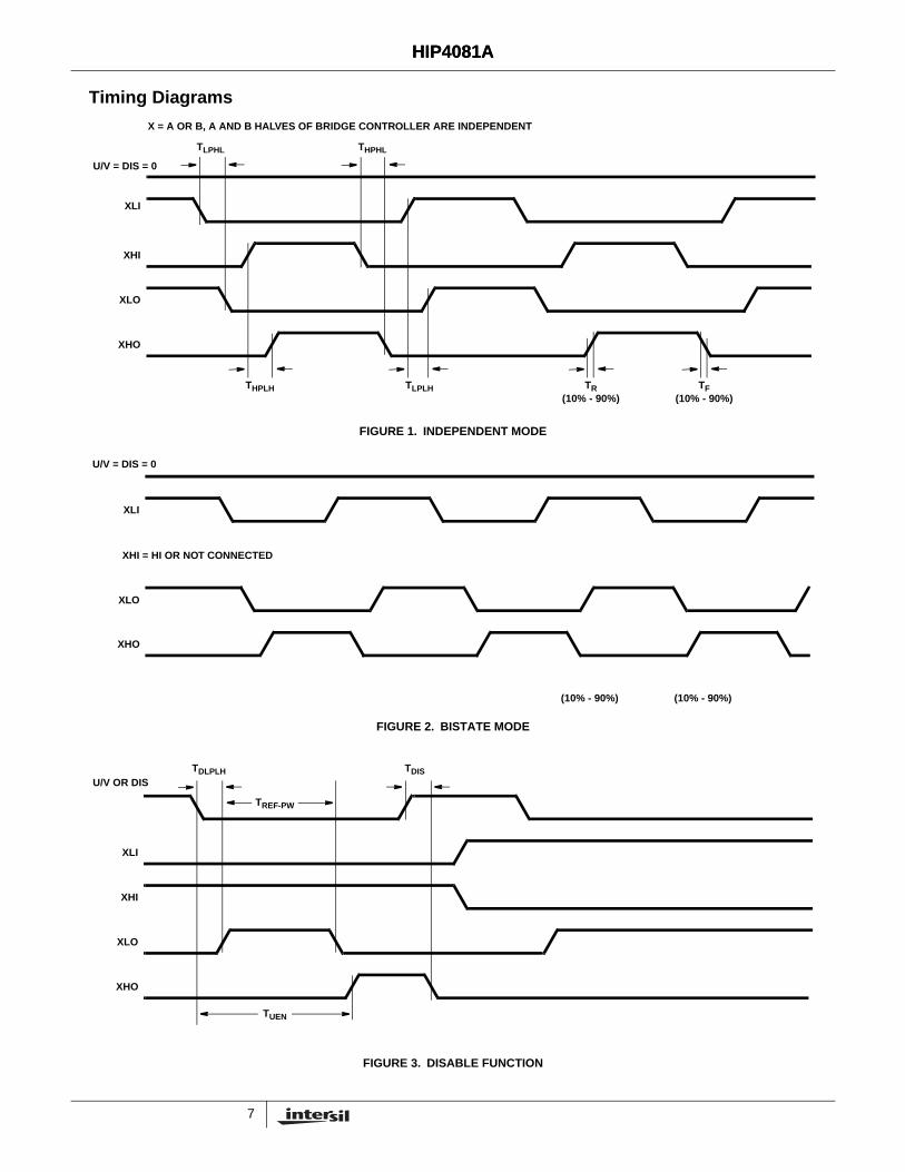
7
HIP4081A
Timing Diagrams
FIGURE 1. INDEPENDENT MODE
FIGURE 2. BISTATE MODE
FIGURE 3. DISABLE FUNCTION
U/V = DIS = 0
XLI
XHI
XLO
XHO
TLPHL THPHL
THPLH TLPLH TR(10% - 90%)
TF(10% - 90%)
X = A OR B, A AND B HALVES OF BRIDGE CONTROLLER ARE INDEPENDENT
U/V = DIS = 0
XLI
XHI = HI OR NOT CONNECTED
XLO
XHO
(10% - 90%) (10% - 90%)
U/V OR DIS
XLI
XHI
XLO
XHO
TDLPLH TDIS
TUEN
TREF-PW
HIP4081A

8
HIP4081A
Typical Performance Curves VDD = VCC = VAHB = VBHB = 12V, VSS = VALS = VBLS = VAHS = VBHS = 0V, RHDEL = RLDEL =
100K and TA = 25oC, Unless Otherwise Specified
FIGURE 4. QUIESCENT IDD SUPPLY CURRENT vs VDD SUPPLY VOLTAGE
FIGURE 5. IDDO, NO-LOAD IDD SUPPLY CURRENT vs FREQUENCY (kHz)
FIGURE 6. SIDE A, B FLOATING SUPPLY BIAS CURRENT vs FREQUENCY (LOAD = 1000pF)
FIGURE 7. ICCO, NO-LOAD ICC SUPPLY CURRENT vs FREQUENCY (kHz) TEMPERATURE
FIGURE 8. IAHB, IBHB, NO-LOAD FLOATING SUPPLY BIAS CURRENT vs FREQUENCY
FIGURE 9. ALI, BLI, AHI, BHI LOW LEVEL INPUT CURRENT IIL vs TEMPERATURE
6 8 10 12 142.0
4.0
6.0
8.0
10.0
12.0
14.0
I DD
SU
PP
LY C
UR
RE
NT
(m
A)
VDD SUPPLY VOLTAGE (V)
0 100 200 300 400 500 600 700 800 900 10008.0
8.5
9.0
9.5
10.0
10.5
11.0
I DD
SU
PP
LY C
UR
RE
NT
(m
A)
SWITCHING FREQUENCY (kHz)
0 100 200 300 400 500 600 700 800 900 10000.0
5.0
10.0
15.0
20.0
25.0
30.0
FL
OA
TIN
G S
UP
PLY
BIA
S C
UR
RE
NT
(m
A)
SWITCHING FREQUENCY (kHz) 0 100 200 300 400 500 600 700 800 900 10000.0
1.0
2.0
3.0
4.0
5.0
I CC
SU
PP
LY C
UR
RE
NT
(m
A)
SWITCHING FREQUENCY (kHz)
75oC
25oC
125oC
-40oC
0oC
0.5
1
1.5
2
2.5
200 600 800 10000 400
FL
OA
TIN
G S
UP
PLY
BIA
S C
UR
RE
NT
(m
A)
SWITCHING FREQUENCY (kHz)
-50 -25 0 25 50 75 100 125-120
-110
-100
-90
LO
W L
EV
EL
INP
UT
CU
RR
EN
T (µA
)
JUNCTION TEMPERATURE (oC)
HIP4081A

HIP4081AHIP4081A
Typical Performance Curves VDD = VCC = VAHB = VBHB = 12V, VSS = VALS = VBLS = VAHS = VBHS = 0V, RHDEL = RLDEL = 10K
and TA = 25oC, Unless Otherwise Specified
FIGURE 10. AHB - AHS, BHB - BHS NO-LOAD CHARGE PUMP VOLTAGE vs TEMPERATURE
FIGURE 11. UPPER DISABLE TURN-OFF PROPAGATION DELAY TDISHIGH vs TEMPERATURE
FIGURE 12. DISABLE TO UPPER ENABLE, TUEN, PROPAGATION DELAY vs TEMPERATURE
FIGURE 13. LOWER DISABLE TURN-OFF PROPAGATION DELAY TDISLOW vs TEMPERATURE
FIGURE 14. TREF-PW REFRESH PULSE WIDTH vs TEMPERATURE
FIGURE 15. DISABLE TO LOWER ENABLE TDLPLH PROPAGATION DELAY vs TEMPERATURE
-40 -20 0 20 40 60 80 100 12010.0
11.0
12.0
13.0
14.0
15.0
NO
-LO
AD
FL
OA
TIN
G C
HA
RG
E P
UM
P V
OLT
AG
E (
V)
JUNCTION TEMPERATURE (oC)-40 -20 0 20 40 60 80 100 120
30
40
50
60
70
80
PR
OPA
GA
TIO
N D
EL
AY
(n
s)
JUNCTION TEMPERATURE (oC)
425
450
475
500
525
-50 -25 0 25 50 75 100 125 150
JUNCTION TEMPERATURE (oC)
PR
OPA
GA
TIO
N D
EL
AY
(n
s)
-40 -20 0 20 40 60 80 100 12030
40
50
60
70
80P
RO
PAG
AT
ION
DE
LA
Y (
ns)
JUNCTION TEMPERATURE (oC)
350
375
400
425
450
-50 -25 0 25 50 75 100 125 150
RE
FR
ES
H P
UL
SE
WID
TH
(n
s)
JUNCTION TEMPERATURE (oC)-40 -20 0 20 40 60 80 100 120
20
30
40
50
60
70
80
PR
OPA
GA
TIO
N D
EL
AY
(n
s)
JUNCTION TEMPERATURE (oC)
9

HIP4081AHIP4081A
FIGURE 16. UPPER TURN-OFF PROPAGATION DELAY THPHL vs TEMPERATURE
FIGURE 17. UPPER TURN-ON PROPAGATION DELAY THPLH vs TEMPERATURE
FIGURE 18. LOWER TURN-OFF PROPAGATION DELAY TLPHL vs TEMPERATURE
FIGURE 19. LOWER TURN-ON PROPAGATION DELAY TLPLH vs TEMPERATURE
FIGURE 20. GATE DRIVE FALL TIME TF vs TEMPERATURE FIGURE 21. GATE DRIVE RISE TIME TR vs TEMPERATURE
Typical Performance Curves VDD = VCC = VAHB = VBHB = 12V, VSS = VALS = VBLS = VAHS = VBHS = 0V, RHDEL = RLDEL = 10K
and TA = 25oC, Unless Otherwise Specified (Continued)
-40 -20 0 20 40 60 80 100 12020
30
40
50
60
70
80
PR
OPA
GA
TIO
N D
EL
AY
(n
s)
JUNCTION TEMPERATURE (oC)-40 -20 0 20 40 60 80 100 120
20
30
40
50
60
70
80
PR
OPA
GA
TIO
N D
EL
AY
(n
s)
JUNCTION TEMPERATURE (oC)
-40 -20 0 20 40 60 80 100 12020
30
40
50
60
70
80
PR
OPA
GA
TIO
N D
EL
AY
(n
s)
JUNCTION TEMPERATURE (oC)
-40 -20 0 20 40 60 80 100 120
20
30
40
50
60
70
80P
RO
PAG
AT
ION
DE
LA
Y (
ns)
JUNCTION TEMPERATURE (oC)
-40 -20 0 20 40 60 80 100 1208.5
9.5
10.5
11.5
12.5
13.5
GA
TE
DR
IVE
FA
LL
TIM
E (
ns)
JUNCTION TEMPERATURE (oC)-40 -20 0 20 40 60 80 100 120
8.5
9.5
10.5
11.5
12.5
13.5
TU
RN
-ON
RIS
E T
IME
(n
s)
JUNCTION TEMPERATURE (oC)
10

HIP4081AHIP4081A
Typical Performance Curves VDD = VCC = VAHB = VBHB = 12V, VSS = VALS = VBLS = VAHS = VBHS = 0V, RHDEL = RLDEL =
100K and TA = 25oC, Unless Otherwise Specified
FIGURE 22. VLDEL, VHDEL VOLTAGE vs TEMPERATURE FIGURE 23. HIGH LEVEL OUTPUT VOLTAGE VCC - VOH vs BIAS SUPPLY AND TEMPERATURE AT 100mA
FIGURE 24. LOW LEVEL OUTPUT VOLTAGE VOL vs BIAS SUPPLY AND TEMPERATURE AT 100mA
FIGURE 25. PEAK PULLDOWN CURRENT IO vs BIAS SUPPLY VOLTAGE
-40 -20 0 20 40 60 80 100 1204.0
4.5
5.0
5.5
6.0
HD
EL
, LD
EL
INP
UT
VO
LTA
GE
(V
)
JUNCTION TEMPERATURE (oC)10 12 140
250
500
750
1000
1250
1500
VC
C -
VO
H (
mV
)
BIAS SUPPLY VOLTAGE (V)
75oC
25oC
125oC
-40oC
0oC
12 140
250
500
750
1000
1250
1500
VO
L (
mV
)
BIAS SUPPLY VOLTAGE (V)10
75oC
25oC
125oC
-40oC
0oC
6 7 8 9 10 11 12 13 14 15 160.0
0.5
1.0
1.5
2.0
2.5
3.0
3.5G
AT
E D
RIV
E S
INK
CU
RR
EN
T (
A)
VDD, VCC, VAHB, VBHB (V)
11
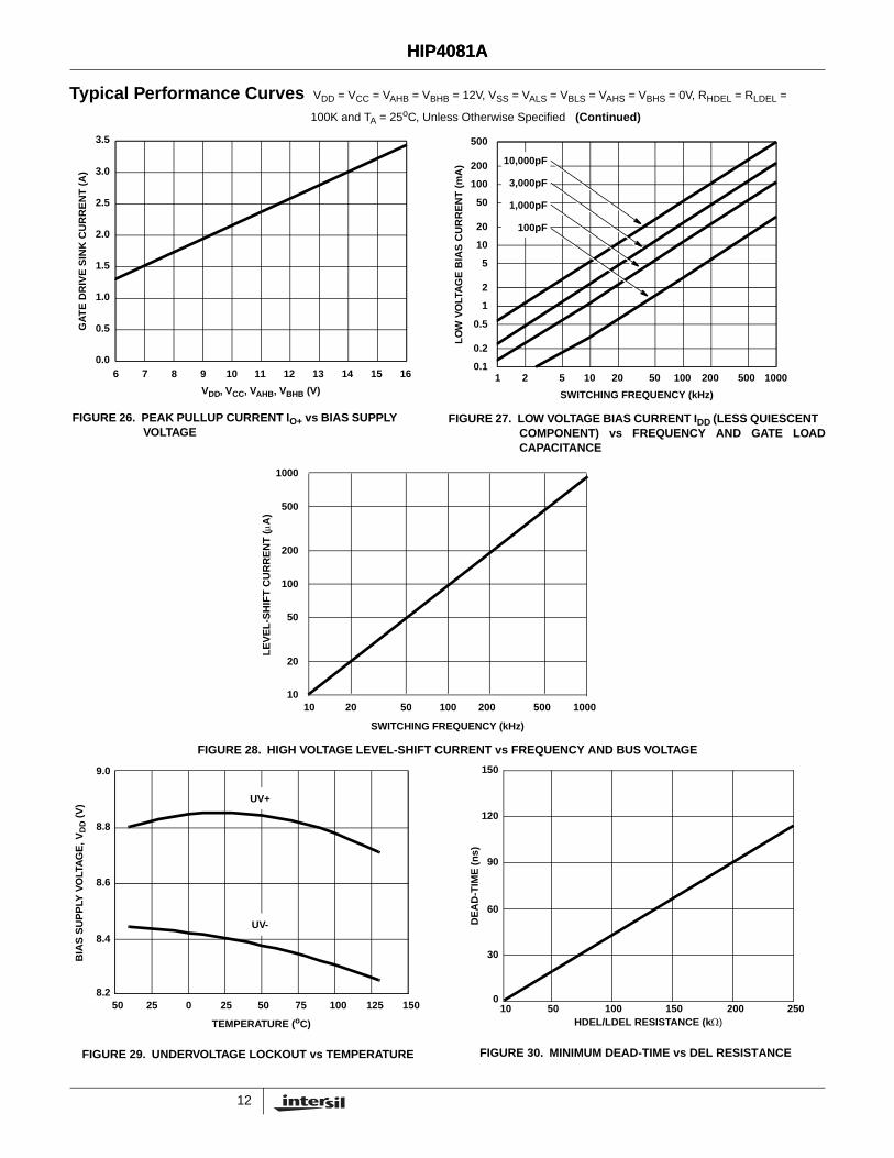
HIP4081AHIP4081A
FIGURE 26. PEAK PULLUP CURRENT IO+ vs BIAS SUPPLY VOLTAGE
FIGURE 27. LOW VOLTAGE BIAS CURRENT IDD (LESS QUIESCENT COMPONENT) vs FREQUENCY AND GATE LOADCAPACITANCE
FIGURE 28. HIGH VOLTAGE LEVEL-SHIFT CURRENT vs FREQUENCY AND BUS VOLTAGE
FIGURE 29. UNDERVOLTAGE LOCKOUT vs TEMPERATURE FIGURE 30. MINIMUM DEAD-TIME vs DEL RESISTANCE
Typical Performance Curves VDD = VCC = VAHB = VBHB = 12V, VSS = VALS = VBLS = VAHS = VBHS = 0V, RHDEL = RLDEL =
100K and TA = 25oC, Unless Otherwise Specified (Continued)
6 7 8 9 10 11 12 13 14 15 160.0
0.5
1.0
1.5
2.0
2.5
3.0
3.5
GA
TE
DR
IVE
SIN
K C
UR
RE
NT
(A
)
VDD, VCC, VAHB, VBHB (V)1 10 100 10002 5 20 50 500200
0.1
1
10
100
500
50
5
0.5
200
20
2
0.2
LO
W V
OLT
AG
E B
IAS
CU
RR
EN
T (
mA
)
SWITCHING FREQUENCY (kHz)
100pF
1,000pF
10,000pF
3,000pF
10 100 100020 50 200 50010
100
1000
20
50
200
500
LE
VE
L-S
HIF
T C
UR
RE
NT
(µA
)
SWITCHING FREQUENCY (kHz)
8.2
8.4
8.6
8.8
9.0
50 25 0 25 50 75 100 125 150
UV+
UV-
TEMPERATURE (oC)
BIA
S S
UP
PLY
VO
LTA
GE
, VD
D (
V)
10 50 100 150 200 2500
30
60
90
120
150
HDEL/LDEL RESISTANCE (kΩ)
DE
AD
-TIM
E (
ns)
12

13
HIP
4081A
1
2
3
1
2
3
1
2
3
65
1
2
3
21
1213
1
2
3
1011
1
2
3
1
2
3
4
5
6
7
8
9
10 11
12
13
14
15
16
17
18
19
20
L1
R21
Q1
Q3
Q4
R22
L2R23 C1
C3
JMPR1
R24
R30 R31
C2
R34
C4
CR2
CR1
Q2
JMP
R5
JMPR3
JMPR2
JMPR4
R33
C5
C6
CX CY
C8
U1
CW CW
+
B+
IN2 IN1
BO
OUT/BLI
IN-/AHI
COM
IN+/ALI +12V
+12V
BLS
AO
HEN/BHI
ALS
CD4069UB
CD4069UB
CD4069UB
CD4069UB
HIP4080A/81A
SECTIONCONTROL LOGIC
POWER SECTION
DRIVER SECTION
AHOAHB
AHSLDEL
ALOHDEL
ALSIN-/AHI
VCCIN+/ALI
VDDOUT/BLI
BLSVSS
BLODIS
BHSHEN/BHI
BHOBHB
R29
U2
U2
U2
U2
43
89
R32
I
O
O
CD4069UB
CD4069UB
ENABLE IN
U2
U2
NOTES:
1. DEVICE CD4069UB PIN 7 = COM, PIN 14 = +12V.
2. COMPONENTS L1, L2, C1, C2, CX, CY, R30, R31, NOT SUPPLIED. REFER TO APPLICATION NOTE FOR DESCRIPTION OF INPUT LOGIC OPERATION TO DETERMINE JUMPER LOCATIONS FOR JMPR1 - JMPR4.
FIGURE 31. HIP4081A EVALUATION PC BOARD SCHEMATIC
HIP
4081A

14
HIP
4081A
R22 1
Q3
L1
JMPR2
JMP
R5
R31
R33
CR2
R23
R24
R27
R28
R26
1
Q4
1
Q2JMPR3
U1
R21
GND
L2
C3
C4
JMPR4
JMPR1
R30
CR1
U2
R34
R32
I
O
C8R29
C7
C6
C5
CY
CX
1
Q1
COM+12V
B+
IN1
IN2
AHO
BHO
ALO
BLOBLS
BLS
LDEL
HD
EL
DIS
ALS
ALS
O
+ +
HIP
4080
/81
FIGURE 32. HIP4081A EVALUATION BOARD SILKSCREEN
HIP
4081A

15
HIP4081A
E20.3 (JEDEC MS-001-AD ISSUE D)20 LEAD DUAL-IN-LINE PLASTIC PACKAGE
SYMBOL
INCHES MILLIMETERS
NOTESMIN MAX MIN MAX
A - 0.210 - 5.33 4
A1 0.015 - 0.39 - 4
A2 0.115 0.195 2.93 4.95 -
B 0.014 0.022 0.356 0.558 -
B1 0.045 0.070 1.55 1.77 8
C 0.008 0.014 0.204 0.355 -
D 0.980 1.060 24.89 26.9 5
D1 0.005 - 0.13 - 5
E 0.300 0.325 7.62 8.25 6
E1 0.240 0.280 6.10 7.11 5
e 0.100 BSC 2.54 BSC -
eA 0.300 BSC 7.62 BSC 6
eB - 0.430 - 10.92 7
L 0.115 0.150 2.93 3.81 4
N 20 20 9
Rev. 0 12/93
NOTES:
1. Controlling Dimensions: INCH. In case of conflict between English and Metric dimensions, the inch dimensions control.
2. Dimensioning and tolerancing per ANSI Y14.5M-1982.
3. Symbols are defined in the “MO Series Symbol List” in Section 2.2 of Publication No. 95.
4. Dimensions A, A1 and L are measured with the package seated in JEDEC seating plane gauge GS-3.
5. D, D1, and E1 dimensions do not include mold flash or protrusions. Mold flash or protrusions shall not exceed 0.010 inch (0.25mm).
6. E and are measured with the leads constrained to be perpendicular to datum .
7. eB and eC are measured at the lead tips with the leads unconstrained. eC must be zero or greater.
8. B1 maximum dimensions do not include dambar protrusions. Dambar protrusions shall not exceed 0.010 inch (0.25mm).
9. N is the maximum number of terminal positions.
10. Corner leads (1, N, N/2 and N/2 + 1) for E8.3, E16.3, E18.3, E28.3, E42.6 will have a B1 dimension of 0.030 - 0.045 inch (0.76 - 1.14mm).
CL
E
eA
C
eB
eC
-B-
E1INDEX
1 2 3 N/2
N
AREA
SEATING
BASEPLANE
PLANE
-C-
D1
B1B
e
D
D1
AA2
L
A1
-A-
0.010 (0.25) C AM B S
eA-C-
Dual-In-Line Plastic Packages (PDIP)
HIP4081A

16
All Intersil U.S. products are manufactured, assembled and tested utilizing ISO9000 quality systems.Intersil Corporation’s quality certifications can be viewed at www.intersil.com/design/quality
Intersil products are sold by description only. Intersil Corporation reserves the right to make changes in circuit design, software and/or specifications at any time withoutnotice. Accordingly, the reader is cautioned to verify that data sheets are current before placing orders. Information furnished by Intersil is believed to be accurate andreliable. However, no responsibility is assumed by Intersil or its subsidiaries for its use; nor for any infringements of patents or other rights of third parties which may resultfrom its use. No license is granted by implication or otherwise under any patent or patent rights of Intersil or its subsidiaries.
For information regarding Intersil Corporation and its products, see www.intersil.com
HIP4081A
NOTES:
1. Symbols are defined in the “MO Series Symbol List” in Section 2.2 of Publication Number 95.
2. Dimensioning and tolerancing per ANSI Y14.5M-1982.
3. Dimension “D” does not include mold flash, protrusions or gate burrs. Mold flash, protrusion and gate burrs shall not exceed 0.15mm (0.006 inch) per side.
4. Dimension “E” does not include interlead flash or protrusions. Interlead flash and protrusions shall not exceed 0.25mm (0.010 inch) per side.
5. The chamfer on the body is optional. If it is not present, a visual index feature must be located within the crosshatched area.
6. “L” is the length of terminal for soldering to a substrate.
7. “N” is the number of terminal positions.
8. Terminal numbers are shown for reference only.
9. The lead width “B”, as measured 0.36mm (0.014 inch) or greater above the seating plane, shall not exceed a maximum value of 0.61mm (0.024 inch)
10. Controlling dimension: MILLIMETER. Converted inch dimensions are not necessarily exact.
INDEXAREA
E
D
N
1 2 3
-B-
0.25(0.010) C AM B S
e
-A-
L
B
M
-C-
A1
A
SEATING PLANE
0.10(0.004)
h x 45o
C
H
µ
0.25(0.010) BM M
α
M20.3 (JEDEC MS-013-AC ISSUE C)20 LEAD WIDE BODY SMALL OUTLINE PLASTIC PACKAGE
SYMBOL
INCHES MILLIMETERS
NOTESMIN MAX MIN MAX
A 0.0926 0.1043 2.35 2.65 -
A1 0.0040 0.0118 0.10 0.30 -
B 0.013 0.0200 0.33 0.51 9
C 0.0091 0.0125 0.23 0.32 -
D 0.4961 0.5118 12.60 13.00 3
E 0.2914 0.2992 7.40 7.60 4
e 0.050 BSC 1.27 BSC -
H 0.394 0.419 10.00 10.65 -
h 0.010 0.029 0.25 0.75 5
L 0.016 0.050 0.40 1.27 6
N 20 20 7
α 0o 8o 0o 8o -
Rev. 0 12/93
Small Outline Plastic Packages (SOIC)
HIP4081AHIP4081A
LF155/LF156/LF256/LF257/LF355/LF356/LF357JFET Input Operational AmplifiersGeneral DescriptionThese are the first monolithic JFET input operational ampli-fiers to incorporate well matched, high voltage JFETs on thesame chip with standard bipolar transistors (BI-FET™ Tech-nology). These amplifiers feature low input bias and offsetcurrents/low offset voltage and offset voltage drift, coupledwith offset adjust which does not degrade drift orcommon-mode rejection. The devices are also designed forhigh slew rate, wide bandwidth, extremely fast settling time,low voltage and current noise and a low 1/f noise corner.
FeaturesAdvantagesn Replace expensive hybrid and module FET op ampsn Rugged JFETs allow blow-out free handling compared
with MOSFET input devicesn Excellent for low noise applications using either high or
low source impedance — very low 1/f cornern Offset adjust does not degrade drift or common-mode
rejection as in most monolithic amplifiersn New output stage allows use of large capacitive loads
(5,000 pF) without stability problemsn Internal compensation and large differential input voltage
capability
Applicationsn Precision high speed integratorsn Fast D/A and A/D convertersn High impedance buffersn Wideband, low noise, low drift amplifiers
n Logarithmic amplifiersn Photocell amplifiersn Sample and Hold circuits
Common Featuresn Low input bias current: 30pAn Low Input Offset Current: 3pAn High input impedance: 1012Ωn Low input noise current:n High common-mode rejection ratio: 100 dBn Large dc voltage gain: 106 dB
Uncommon FeaturesLF155/LF355
LF156/LF256/LF356
LF257/LF357(AV=5)
Units
j Extremelyfast settlingtime to0.01%
4 1.5 1.5 µs
j Fast slewrate
5 12 50 V/µs
j Wide gainbandwidth
2.5 5 20 MHz
j Low inputnoisevoltage
20 12 12
Simplified Schematic
00564601
*3pF in LF357 series.
BI-FET™, BI-FET II™ are trademarks of National Semiconductor Corporation.
December 2001LF155/LF156/LF256/LF257/LF355/LF356/LF357
JFET
InputOperationalA
mplifiers
© 2001 National Semiconductor Corporation DS005646 www.national.com
Absolute Maximum Ratings (Note 1)
If Military/Aerospace specified devices are required, contact the National Semiconductor Sales Office/Distributors foravailability and specifications.
LF155/6 LF256/7/LF356B LF355/6/7
Supply Voltage ±22V ±22V ±18V
Differential Input Voltage ±40V ±40V ±30V
Input Voltage Range (Note 2) ±20V ±20V ±16V
Output Short Circuit Duration Continuous Continuous Continuous
TJMAX
H-Package 150˚C 115˚C 115˚C
N-Package 100˚C 100˚C
M-Package 100˚C 100˚C
Power Dissipation at TA = 25˚C (Notes1, 8)
H-Package (Still Air) 560 mW 400 mW 400 mW
H-Package (400 LF/Min Air Flow) 1200 mW 1000 mW 1000 mW
N-Package 670 mW 670 mW
M-Package 380 mW 380 mW
Thermal Resistance (Typical) θJA
H-Package (Still Air) 160˚C/W 160˚C/W 160˚C/W
H-Package (400 LF/Min Air Flow) 65˚C/W 65˚C/W 65˚C/W
N-Package 130˚C/W 130˚C/W
M-Package 195˚C/W 195˚C/W
(Typical) θJC
H-Package 23˚C/W 23˚C/W 23˚C/W
Storage Temperature Range −65˚C to +150˚C −65˚C to +150˚C −65˚C to +150˚C
Soldering Information (Lead Temp.)
Metal Can Package
Soldering (10 sec.) 300˚C 300˚C 300˚C
Dual-In-Line Package
Soldering (10 sec.) 260˚C 260˚C 260˚C
Small Outline Package
Vapor Phase (60 sec.) 215˚C 215˚C
Infrared (15 sec.) 220˚C 220˚C
See AN-450 “Surface Mounting Methods and Their Effect on Product Reliability” for other methods ofsoldering surface mount devices.
ESD tolerance
(100 pF discharged through 1.5kΩ) 1000V 1000V 1000V
DC Electrical Characteristics(Note 3)
Symbol Parameter ConditionsLF155/6
LF256/7LF356B
LF355/6/7Units
Min Typ Max Min Typ Max Min Typ Max
VOS Input Offset Voltage RS=50Ω, TA=25˚C 3 5 3 5 3 10 mV
Over Temperature 7 6.5 13 mV
∆VOS/∆T Average TC of InputOffset Voltage
RS=50Ω5 5 5 µV/˚C
∆TC/∆VOS Change in Average TCwith VOS Adjust
RS=50Ω, (Note 4)0.5 0.5 0.5
µV/˚Cper mV
IOS Input Offset Current TJ=25˚C, (Notes 3, 5) 3 20 3 20 3 50 pA
TJ≤THIGH 20 1 2 nA
LF15
5/LF
156/
LF25
6/LF
257/
LF35
5/LF
356/
LF35
7
www.national.com 2

DC Electrical Characteristics (Continued)(Note 3)
Symbol Parameter ConditionsLF155/6
LF256/7LF356B
LF355/6/7Units
Min Typ Max Min Typ Max Min Typ Max
IB Input Bias Current TJ=25˚C, (Notes 3, 5) 30 100 30 100 30 200 pA
TJ≤THIGH 50 5 8 nA
RIN Input Resistance TJ=25˚C 1012 1012 1012 ΩAVOL Large Signal Voltage
GainVS=±15V, TA=25˚C 50 200 50 200 25 200 V/mV
VO=±10V, RL=2k
Over Temperature 25 25 15 V/mV
VO Output Voltage Swing VS=±15V, RL=10k ±12 ±13 ±12 ±13 ±12 ±13 V
VS=±15V, RL=2k ±10 ±12 ±10 ±12 ±10 ±12 V
VCM Input Common-ModeVoltage Range
VS=±15V±11
+15.1±11
±15.1+10
+15.1 V
−12 −12 −12 V
CMRR Common-ModeRejection Ratio
85 100 85 100 80 100 dB
PSRR Supply VoltageRejection Ratio
(Note 6)85 100 85 100 80 100 dB
DC Electrical CharacteristicsTA = TJ = 25˚C, VS = ±15V
ParameterLF155 LF355 LF156/256/257/356B LF356 LF357
UnitsTyp Max Typ Max Typ Max Typ Max Typ Max
SupplyCurrent
2 4 2 4 5 7 5 10 5 10 mA
AC Electrical CharacteristicsTA = TJ = 25˚C, VS = ±15V
Symbol Parameter Conditions
LF155/355 LF156/256/356B
LF156/256/356/LF356B
LF257/357
Units
Typ Min Typ Typ
SR Slew Rate LF155/6:AV=1,
5 7.5 12 V/µs
LF357: AV=5 50 V/µs
GBW Gain Bandwidth Product 2.5 5 20 MHz
ts Settling Time to 0.01% (Note 7) 4 1.5 1.5 µs
en Equivalent Input NoiseVoltage
RS=100Ωf=100 Hz 25 15 15
f=1000 Hz 20 12 12
in Equivalent Input CurrentNoise
f=100 Hz 0.01 0.01 0.01
f=1000 Hz 0.01 0.01 0.01
CIN Input Capacitance 3 3 3 pF
Notes for Electrical CharacteristicsNote 1: The maximum power dissipation for these devices must be derated at elevated temperatures and is dictated by TJMAX, θJA, and the ambient temperature,TA. The maximum available power dissipation at any temperature is PD=(TJMAX−TA)/θJA or the 25˚C PdMAX, whichever is less.
Note 2: Unless otherwise specified the absolute maximum negative input voltage is equal to the negative power supply voltage.
Note 3: Unless otherwise stated, these test conditions apply:
LF155/LF156/LF256/LF257/LF355/LF356/LF357
www.national.com3
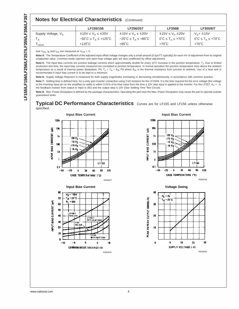
Notes for Electrical Characteristics (Continued)
LF155/156 LF256/257 LF356B LF355/6/7
Supply Voltage, VS ±15V ≤ VS ≤ ±20V ±15V ≤ VS ≤ ±20V ±15V ≤ VS ±20V VS= ±15V
TA −55˚C ≤ TA ≤ +125˚C −25˚C ≤ TA ≤ +85˚C 0˚C ≤ TA ≤ +70˚C 0˚C ≤ TA ≤ +70˚C
THIGH +125˚C +85˚C +70˚C +70˚C
and VOS, IB and IOS are measured at VCM = 0.
Note 4: The Temperature Coefficient of the adjusted input offset voltage changes only a small amount (0.5µV/˚C typically) for each mV of adjustment from its originalunadjusted value. Common-mode rejection and open loop voltage gain are also unaffected by offset adjustment.
Note 5: The input bias currents are junction leakage currents which approximately double for every 10˚C increase in the junction temperature, TJ. Due to limitedproduction test time, the input bias currents measured are correlated to junction temperature. In normal operation the junction temperature rises above the ambienttemperature as a result of internal power dissipation, Pd. TJ = TA + θJA Pd where θJA is the thermal resistance from junction to ambient. Use of a heat sink isrecommended if input bias current is to be kept to a minimum.
Note 6: Supply Voltage Rejection is measured for both supply magnitudes increasing or decreasing simultaneously, in accordance with common practice.
Note 7: Settling time is defined here, for a unity gain inverter connection using 2 kΩ resistors for the LF155/6. It is the time required for the error voltage (the voltageat the inverting input pin on the amplifier) to settle to within 0.01% of its final value from the time a 10V step input is applied to the inverter. For the LF357, AV = −5,the feedback resistor from output to input is 2kΩ and the output step is 10V (See Settling Time Test Circuit).
Note 8: Max. Power Dissipation is defined by the package characteristics. Operating the part near the Max. Power Dissipation may cause the part to operate outsideguaranteed limits.
Typical DC Performance Characteristics Curves are for LF155 and LF156 unless otherwisespecified.
Input Bias Current Input Bias Current
00564637 00564638
Input Bias Current Voltage Swing
00564639 00564640
LF15
5/LF
156/
LF25
6/LF
257/
LF35
5/LF
356/
LF35
7
www.national.com 4

Typical DC Performance Characteristics Curves are for LF155 and LF156 unless otherwisespecified. (Continued)
Supply Current Supply Current
00564641 00564642
Negative Current Limit Positive Current Limit
00564643 00564644
Positive Common-ModeInput Voltage Limit
Negative Common-ModeInput Voltage Limit
00564645
00564646
LF155/LF156/LF256/LF257/LF355/LF356/LF357
www.national.com5

Typical DC Performance Characteristics Curves are for LF155 and LF156 unless otherwisespecified. (Continued)
Open Loop Voltage Gain Output Voltage Swing
00564647 00564648
Typical AC Performance CharacteristicsGain Bandwidth Gain Bandwidth
0056464900564650
Normalized Slew Rate Output Impedance
0056465100564652
LF15
5/LF
156/
LF25
6/LF
257/
LF35
5/LF
356/
LF35
7
www.national.com 6

Typical AC Performance Characteristics (Continued)
Output Impedance LF155 Small Signal Pulse Response, A V = +1
00564653
00564605
LF156 Small Signal Pulse Response, A V = +1 LF155 Large Signal Pulse Response, A V = +1
00564606 00564608
LF156 Large Signal PulsResponse, A V = +1 Inverter Settling Time
00564609
00564655
LF155/LF156/LF256/LF257/LF355/LF356/LF357
www.national.com7
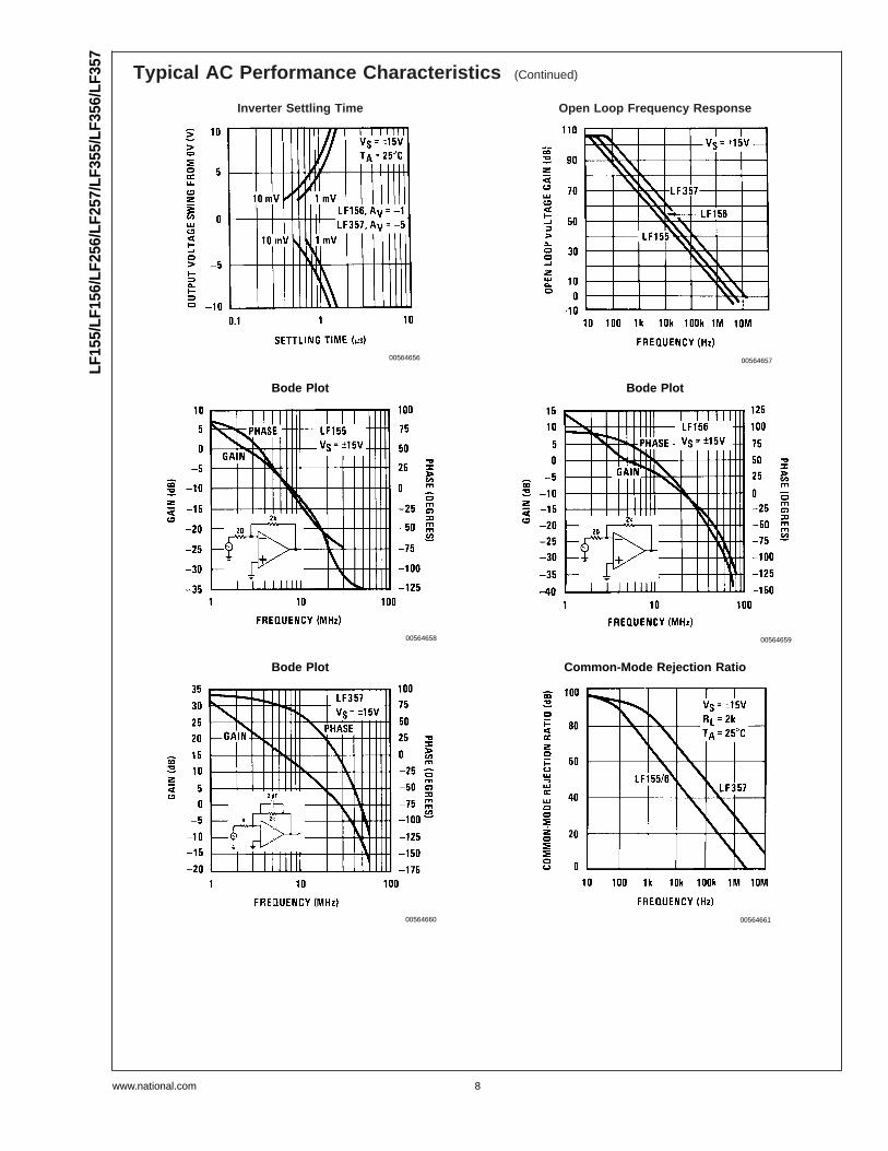
Typical AC Performance Characteristics (Continued)
Inverter Settling Time Open Loop Frequency Response
00564656 00564657
Bode Plot Bode Plot
00564658 00564659
Bode Plot Common-Mode Rejection Ratio
00564660 00564661
LF15
5/LF
156/
LF25
6/LF
257/
LF35
5/LF
356/
LF35
7
www.national.com 8

Typical AC Performance Characteristics (Continued)
Power Supply Rejection Ratio Power Supply Rejection Ratio
00564662 00564663
Undistorted Output Voltage Swing Equivalent Input Noise Voltage
00564664
00564665
Equivalent Input NoiseVoltage (Expanded Scale)
00564666
LF155/LF156/LF256/LF257/LF355/LF356/LF357
www.national.com9

Detailed Schematic
00564613
*C = 3pF in LF357 series.
Connection Diagrams (Top Views)
Metal Can Package (H)
00564614
Order Number LF155H, LF156H, LF256H, LF257H,LF356BH, LF356H, or LF357H
See NS Package Number H08C*Available per JM38510/11401 or JM38510/11402
Dual-In-Line Package (M and N)
00564629
Order Number LF356M, LF356MX, LF355N, or LF356NSee NS Package Number M08A or N08E
Application HintsThese are op amps with JFET input devices. These JFETshave large reverse breakdown voltages from gate to sourceand drain eliminating the need for clamps across the inputs.Therefore large differential input voltages can easily be ac-commodated without a large increase in input current. Themaximum differential input voltage is independent of thesupply voltages. However, neither of the input voltagesshould be allowed to exceed the negative supply as this willcause large currents to flow which can result in a destroyedunit.
Exceeding the negative common-mode limit on either inputwill force the output to a high state, potentially causing a
LF15
5/LF
156/
LF25
6/LF
257/
LF35
5/LF
356/
LF35
7
www.national.com 10

Application Hints (Continued)
reversal of phase to the output. Exceeding the negativecommon-mode limit on both inputs will force the amplifieroutput to a high state. In neither case does a latch occursince raising the input back within the common-mode rangeagain puts the input stage and thus the amplifier in a normaloperating mode.
Exceeding the positive common-mode limit on a single inputwill not change the phase of the output however, if bothinputs exceed the limit, the output of the amplifier will beforced to a high state.
These amplifiers will operate with the common-mode inputvoltage equal to the positive supply. In fact, thecommon-mode voltage can exceed the positive supply byapproximately 100 mV independent of supply voltage andover the full operating temperature range. The positive sup-ply can therefore be used as a reference on an input as, forexample, in a supply current monitor and/or limiter.
Precautions should be taken to ensure that the power supplyfor the integrated circuit never becomes reversed in polarityor that the unit is not inadvertently installed backwards in asocket as an unlimited current surge through the resultingforward diode within the IC could cause fusing of the internalconductors and result in a destroyed unit.
All of the bias currents in these amplifiers are set by FETcurrent sources. The drain currents for the amplifiers aretherefore essentially independent of supply voltage.
As with most amplifiers, care should be taken with leaddress, component placement and supply decoupling in orderto ensure stability. For example, resistors from the output toan input should be placed with the body close to the input tominimize “pickup” and maximize the frequency of the feed-back pole by minimizing the capacitance from the input toground.
A feedback pole is created when the feedback around anyamplifier is resistive. The parallel resistance and capacitancefrom the input of the device (usually the inverting input) to ACground set the frequency of the pole. In many instances thefrequency of this pole is much greater than the expected 3dBfrequency of the closed loop gain and consequently there isnegligible effect on stability margin. However, if the feedbackpole is less than approximately six times the expected 3 dBfrequency a lead capacitor should be placed from the outputto the input of the op amp. The value of the added capacitorshould be such that the RC time constant of this capacitorand the resistance it parallels is greater than or equal to theoriginal feedback pole time constant.
Typical Circuit ConnectionsVOS Adjustment
00564667
• VOS is adjusted with a 25k potentiometer
• The potentiometer wiper is connected to V+
• For potentiometers with temperature coefficient of 100ppm/˚C or less the additional drift with adjust is ≈ 0.5µV/˚C/mV of adjustment
• Typical overall drift: 5µV/˚C ±(0.5µV/˚C/mV of adj.)
Driving Capacitive Loads
00564668
* LF155/6 R = 5k
LF357 R = 1.25k
Due to a unique output stage design, these amplifiershave the ability to drive large capacitive loads and stillmaintain stability. CL(MAX) . 0.01µF.
Overshoot ≤ 20%
Settling time (ts) . 5µs
LF357. A Large Power BW Amplifier
00564615
For distortion ≤ 1% and a 20 Vp-p VOUT swing, power bandwidth is:500kHz.
LF155/LF156/LF256/LF257/LF355/LF356/LF357
www.national.com11

Typical ApplicationsSettling Time Test Circuit
00564616
• Settling time is tested with the LF155/6 connected as unity gain inverter and LF357 connected for AV = −5
• FET used to isolate the probe capacitance
• Output = 10V step
• AV = −5 for LF357
Large Signal Inverter Output, V OUT (from Settling Time Circuit)
LF355
00564617
LF356
00564618
LF357
00564619
LF15
5/LF
156/
LF25
6/LF
257/
LF35
5/LF
356/
LF35
7
www.national.com 12

Typical Applications (Continued)
Low Drift Adjustable Voltage Reference
00564620
• ∆ VOUT/∆T = ±0.002%/˚C
• All resistors and potentiometers should be wire-wound
• P1: drift adjust
• P2: VOUT adjust
• Use LF155 for
j Low IBj Low drift
j Low supply current
Fast Logarithmic Converter
00564621
• Dynamic range: 100µA ≤ Ii ≤ 1mA (5 decades), |VO| = 1V/decade
• Transient response: 3µs for ∆Ii = 1 decade
• C1, C2, R2, R3: added dynamic compensation
• VOS adjust the LF156 to minimize quiescent error
• RT: Tel Labs type Q81 + 0.3%/˚C
LF155/LF156/LF256/LF257/LF355/LF356/LF357
www.national.com13

Typical Applications (Continued)
Precision Current Monitor
00564631
• VO = 5 R1/R2 (V/mA of IS)
• R1, R2, R3: 0.1% resistors
• Use LF155 for
j Common-mode range to supply range
j Low IBj Low VOS
j Low Supply Current
8-Bit D/A Converter with Symmetrical Offset Binary Operation
00564632
• R1, R2 should be matched within ±0.05%
• Full-scale response time: 3µs
EO B1 B2 B3 B4 B5 B6 B7 B8 Comments
+9.920 1 1 1 1 1 1 1 1 Positive Full-Scale
+0.040 1 0 0 0 0 0 0 0 (+) Zero-Scale
−0.040 0 1 1 1 1 1 1 1 (−) Zero-Scale
−9.920 0 0 0 0 0 0 0 0 Negative Full-Scale
LF15
5/LF
156/
LF25
6/LF
257/
LF35
5/LF
356/
LF35
7
www.national.com 14

Typical Applications (Continued)
Wide BW Low Noise, Low Drift Amplifier
00564670
• Parasitic input capacitance C1 . (3pF for LF155, LF156 and LF357 plus any additional layout capacitance) interacts withfeedback elements and creates undesirable high frequency pole. To compensate add C2 such that: R2 C2 . R1 C1.
Boosting the LF156 with a Current Amplifier
00564673
• IOUT(MAX).150mA (will drive RL≥ 100Ω)
• No additional phase shift added by the current amplifier
LF155/LF156/LF256/LF257/LF355/LF356/LF357
www.national.com15

Typical Applications (Continued)
3 Decades VCO
00564624
R1, R4 matched. Linearity 0.1% over 2 decades.
Isolating Large Capacitive Loads
00564622
• Overshoot 6%
• ts 10µs
• When driving large CL, the VOUT slew rate determined by CL and IOUT(MAX):
LF15
5/LF
156/
LF25
6/LF
257/
LF35
5/LF
356/
LF35
7
www.national.com 16

Typical Applications (Continued)
Low Drift Peak Detector
00564623
• By adding D1 and Rf, VD1=0 during hold mode. Leakage of D2 provided by feedback path through Rf.
• Leakage of circuit is essentially Ib (LF155, LF156) plus capacitor leakage of Cp.
• Diode D3 clamps VOUT (A1) to VIN−VD3 to improve speed and to limit reverse bias of D2.
• Maximum input frequency should be << 1⁄2πRfCD2 where CD2 is the shunt capacitance of D2.
Non-Inverting Unity Gain Operation for LF157
00564675
Inverting Unity Gain for LF157
00564625
LF155/LF156/LF256/LF257/LF355/LF356/LF357
www.national.com17

Typical Applications (Continued)
High Impedance, Low Drift Instrumentation Amplifier
00564626
• System VOS adjusted via A2 VOS adjust
• Trim R3 to boost up CMRR to 120 dB. Instrumentation amplifier resistor array recommended for best accuracy and lowest drift
LF15
5/LF
156/
LF25
6/LF
257/
LF35
5/LF
356/
LF35
7
www.national.com 18

Typical Applications (Continued)
Fast Sample and Hold
00564633
• Both amplifiers (A1, A2) have feedback loops individually closed with stable responses (overshoot negligible)
• Acquisition time TA, estimated by:
• LF156 develops full Sr output capability for VIN ≥ 1V
• Addition of SW2 improves accuracy by putting the voltage drop across SW1 inside the feedback loop
• Overall accuracy of system determined by the accuracy of both amplifiers, A1 and A2
LF155/LF156/LF256/LF257/LF355/LF356/LF357
www.national.com19
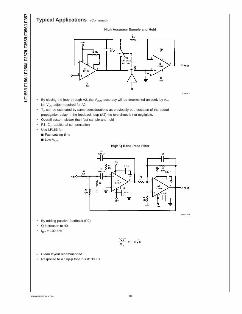
Typical Applications (Continued)
High Accuracy Sample and Hold
00564627
• By closing the loop through A2, the VOUT accuracy will be determined uniquely by A1.
No VOS adjust required for A2.
• TA can be estimated by same considerations as previously but, because of the added
propagation delay in the feedback loop (A2) the overshoot is not negligible.
• Overall system slower than fast sample and hold
• R1, CC: additional compensation
• Use LF156 for
j Fast settling time
j Low VOS
High Q Band Pass Filter
00564628
• By adding positive feedback (R2)
• Q increases to 40
• fBP = 100 kHz
• Clean layout recommended
• Response to a 1Vp-p tone burst: 300µs
LF15
5/LF
156/
LF25
6/LF
257/
LF35
5/LF
356/
LF35
7
www.national.com 20
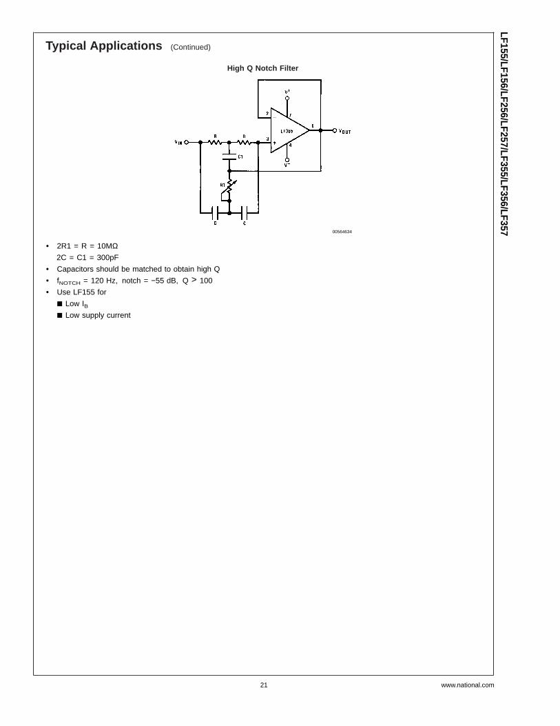
Typical Applications (Continued)
High Q Notch Filter
00564634
• 2R1 = R = 10MΩ2C = C1 = 300pF
• Capacitors should be matched to obtain high Q
• fNOTCH = 120 Hz, notch = −55 dB, Q > 100
• Use LF155 for
j Low IBj Low supply current
LF155/LF156/LF256/LF257/LF355/LF356/LF357
www.national.com21
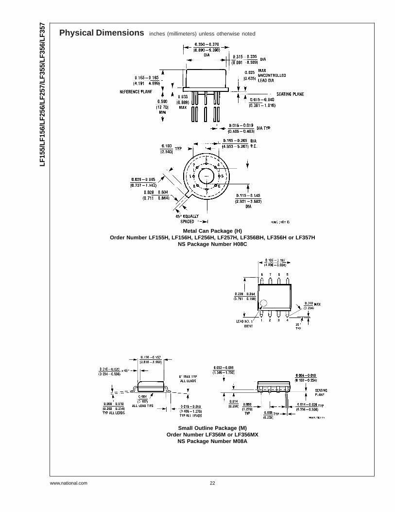
Physical Dimensions inches (millimeters) unless otherwise noted
Metal Can Package (H)Order Number LF155H, LF156H, LF256H, LF257H, LF356BH, LF356H or LF357H
NS Package Number H08C
Small Outline Package (M)Order Number LF356M or LF356MX
NS Package Number M08A
LF15
5/LF
156/
LF25
6/LF
257/
LF35
5/LF
356/
LF35
7
www.national.com 22
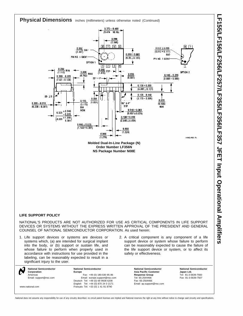
Physical Dimensions inches (millimeters) unless otherwise noted (Continued)
Molded Dual-In-Line Package (N)Order Number LF356N
NS Package Number N08E
LIFE SUPPORT POLICY
NATIONAL’S PRODUCTS ARE NOT AUTHORIZED FOR USE AS CRITICAL COMPONENTS IN LIFE SUPPORTDEVICES OR SYSTEMS WITHOUT THE EXPRESS WRITTEN APPROVAL OF THE PRESIDENT AND GENERALCOUNSEL OF NATIONAL SEMICONDUCTOR CORPORATION. As used herein:
1. Life support devices or systems are devices orsystems which, (a) are intended for surgical implantinto the body, or (b) support or sustain life, andwhose failure to perform when properly used inaccordance with instructions for use provided in thelabeling, can be reasonably expected to result in asignificant injury to the user.
2. A critical component is any component of a lifesupport device or system whose failure to performcan be reasonably expected to cause the failure ofthe life support device or system, or to affect itssafety or effectiveness.
National SemiconductorCorporationAmericasEmail: [email protected]
National SemiconductorEurope
Fax: +49 (0) 180-530 85 86Email: [email protected]
Deutsch Tel: +49 (0) 69 9508 6208English Tel: +44 (0) 870 24 0 2171Français Tel: +33 (0) 1 41 91 8790
National SemiconductorAsia Pacific CustomerResponse GroupTel: 65-2544466Fax: 65-2504466Email: [email protected]
National SemiconductorJapan Ltd.Tel: 81-3-5639-7560Fax: 81-3-5639-7507
www.national.com
LF155/LF156/LF256/LF257/LF355/LF356/LF357JFE
TInputO
perationalAm
plifiers
National does not assume any responsibility for use of any circuitry described, no circuit patent licenses are implied and National reserves the right at any time without notice to change said circuitry and specifications.

SN54HC74, SN74HC74DUAL D-TYPE POSITIVE-EDGE-TRIGGERED FLIP-FLOPS
WITH CLEAR AND PRESET
SCLS094D – DECEMBER 1982 – REVISED JULY 2003
1POST OFFICE BOX 655303 • DALLAS, TEXAS 75265
Wide Operating Voltage Range of 2 V to 6 V
Outputs Can Drive Up To 10 LSTTL Loads
Low Power Consumption, 40-µA Max ICC Typical tpd = 15 ns
±4-mA Output Drive at 5 V
Low Input Current of 1 µA Max
description/ordering information
The ’HC74 devices contain two independentD-type positive-edge-triggered flip-flops. A lowlevel at the preset (PRE) or clear (CLR) inputs setsor resets the outputs, regardless of the levels ofthe other inputs. When PRE and CLR are inactive(high), data at the data (D) input meeting the setuptime requirements are transferred to the outputson the positive-going edge of the clock (CLK)pulse. Clock triggering occurs at a voltage leveland is not directly related to the rise time of CLK.Following the hold-time interval, data at theD input can be changed without affecting thelevels at the outputs.
ORDERING INFORMATION
TA PACKAGE† ORDERABLEPART NUMBER
TOP-SIDEMARKING
PDIP – N Tube of 25 SN74HC74N SN74HC74N
Tube of 50 SN74HC74D
SOIC – D Reel of 2500 SN74HC74DR HC74
Reel of 250 SN74HC74DT
–40°C to 85°C SOP – NS Reel of 2000 SN74HC74NSR HC74
SSOP – DB Reel of 2000 SN74HC74DBR HC74
Tube of 90 SN74HC74PW
TSSOP – PW Reel of 2000 SN74HC74PWR HC74
Reel of 250 SN74HC74PWT
CDIP – J Tube of 25 SNJ54HC74J SNJ54HC74J
–55°C to 125°C CFP – W Tube of 150 SNJ54HC74W SNJ54HC74W
LCCC – FK Tube of 55 SNJ54HC74FK SNJ54HC74FK† Package drawings, standard packing quantities, thermal data, symbolization, and PCB design guidelines are
available at www.ti.com/sc/package.
1
2
3
4
5
6
7
14
13
12
11
10
9
8
1CLR1D
1CLK1PRE
1Q1Q
GND
VCC2CLR2D2CLK2PRE2Q2Q
SN54HC74 . . . J OR W PACKAGESN74HC74 . . . D, DB, N, NS, OR PW PACKAGE
(TOP VIEW)
3 2 1 20 19
9 10 11 12 13
4
5
6
7
8
18
17
16
15
14
2DNC2CLKNC2PRE
1CLKNC
1PRENC1Q
1D 1CLR
NC
2Q 2QV 2C
LR
1QG
ND
NC
SN54HC74 . . . FK PACKAGE(TOP VIEW)
CC
NC – No internal connection
Copyright 2003, Texas Instruments Incorporated
Please be aware that an important notice concerning availability, standard warranty, and use in critical applications ofTexas Instruments semiconductor products and disclaimers thereto appears at the end of this data sheet.
PRODUCTION DATA information is current as of publication date.Products conform to specifications per the terms of Texas Instrumentsstandard warranty. Production processing does not necessarily includetesting of all parameters.
On products compliant to MIL-PRF-38535, all parameters are testedunless otherwise noted. On all other products, productionprocessing does not necessarily include testing of all parameters.

SN54HC74, SN74HC74DUAL D-TYPE POSITIVE-EDGE-TRIGGERED FLIP-FLOPSWITH CLEAR AND PRESET
SCLS094D – DECEMBER 1982 – REVISED JULY 2003
2 POST OFFICE BOX 655303 • DALLAS, TEXAS 75265
FUNCTION TABLE
INPUTS OUTPUTS
PRE CLR CLK D Q Q
L H X X H L
H L X X L H
L L X X H† H†
H H ↑ H H L
H H ↑ L L H
H H L X Q0 Q0† This configuration is nonstable; that is, it does not
persist when PRE or CLR returns to its inactive(high) level.
logic diagram (positive logic)
PRE
CLK
D
CLR
Q
Q
C
C
C
C
C
C
C
C
C
C
TG
TG TG TG
absolute maximum ratings over operating free-air temperature range (unless otherwise noted)‡
Supply voltage range, VCC –0.5 V to 7 V. . . . . . . . . . . . . . . . . . . . . . . . . . . . . . . . . . . . . . . . . . . . . . . . . . . . . . . . . . Input clamp current, IIK (VI < 0 or VI > VCC) (see Note 1) ±20 mA. . . . . . . . . . . . . . . . . . . . . . . . . . . . . . . . . . . . Output clamp current, IOK (VO < 0 or VO > VCC) (see Note 1) ±20 mA. . . . . . . . . . . . . . . . . . . . . . . . . . . . . . . . Continuous output current, IO (VO = 0 to VCC) ±25 mA. . . . . . . . . . . . . . . . . . . . . . . . . . . . . . . . . . . . . . . . . . . . . . Continuous current through VCC or GND ±50 mA. . . . . . . . . . . . . . . . . . . . . . . . . . . . . . . . . . . . . . . . . . . . . . . . . . . Package thermal impedance, θJA (see Note 2): D package 86°C/W. . . . . . . . . . . . . . . . . . . . . . . . . . . . . . . . . . .
DB package 96°C/W. . . . . . . . . . . . . . . . . . . . . . . . . . . . . . . . . N package 80°C/W. . . . . . . . . . . . . . . . . . . . . . . . . . . . . . . . . . . NS package 76°C/W. . . . . . . . . . . . . . . . . . . . . . . . . . . . . . . . . PW package 113°C/W. . . . . . . . . . . . . . . . . . . . . . . . . . . . . . . .
Storage temperature range, Tstg –65°C to 150°C. . . . . . . . . . . . . . . . . . . . . . . . . . . . . . . . . . . . . . . . . . . . . . . . . . .
‡ Stresses beyond those listed under “absolute maximum ratings” may cause permanent damage to the device. These are stress ratings only, andfunctional operation of the device at these or any other conditions beyond those indicated under “recommended operating conditions” is notimplied. Exposure to absolute-maximum-rated conditions for extended periods may affect device reliability.
NOTES: 1. The input and output voltage ratings may be exceeded if the input and output current ratings are observed.2. The package thermal impedance is calculated in accordance with JESD 51-7.

SN54HC74, SN74HC74DUAL D-TYPE POSITIVE-EDGE-TRIGGERED FLIP-FLOPS
WITH CLEAR AND PRESET
SCLS094D – DECEMBER 1982 – REVISED JULY 2003
3POST OFFICE BOX 655303 • DALLAS, TEXAS 75265
recommended operating conditions (see Note 3)
SN54HC74 SN74HC74UNIT
MIN NOM MAX MIN NOM MAXUNIT
VCC Supply voltage 2 5 6 2 5 6 V
VCC = 2 V 1.5 1.5
VIH High-level input voltage VCC = 4.5 V 3.15 3.15 V
VCC = 6 V 4.2 4.2
VCC = 2 V 0.5 0.5
VIL Low-level input voltage VCC = 4.5 V 1.35 1.35 V
VCC = 6 V 1.8 1.8
VI Input voltage 0 VCC 0 VCC V
VO Output voltage 0 VCC 0 VCC V
VCC = 2 V 1000 1000
∆t/∆v Input transition rise/fall time VCC = 4.5 V 500 500 ns
VCC = 6 V 400 400
TA Operating free-air temperature –55 125 –40 85 °C
NOTE 3: All unused inputs of the device must be held at VCC or GND to ensure proper device operation. Refer to the TI application report,Implications of Slow or Floating CMOS Inputs, literature number SCBA004.
electrical characteristics over recommended operating free-air temperature range (unlessotherwise noted)
PARAMETER TEST CONDITIONS VCCTA = 25°C SN54HC74 SN74HC74
UNITPARAMETER TEST CONDITIONS VCCMIN TYP MAX MIN MAX MIN MAX
UNIT
2 V 1.9 1.998 1.9 1.9
IOH = –20 µA 4.5 V 4.4 4.499 4.4 4.4
VOH VI = VIH or VIL 6 V 5.9 5.999 5.9 5.9 V
IOH = –4 mA 4.5 V 3.98 4.3 3.7 3.84
IOH = –5.2 mA 6 V 5.48 5.8 5.2 5.34
2 V 0.002 0.1 0.1 0.1
IOL = 20 µA 4.5 V 0.001 0.1 0.1 0.1
VOL VI = VIH or VIL 6 V 0.001 0.1 0.1 0.1 V
IOL = 4 mA 4.5 V 0.17 0.26 0.4 0.33
IOL = 5.2 mA 6 V 0.15 0.26 0.4 0.33
II VI = VCC or 0 6 V ±0.1 ±100 ±1000 ±1000 nA
ICC VI = VCC or 0, IO = 0 6 V 4 80 40 µA
Ci 2 V to 6 V 3 10 10 10 pF
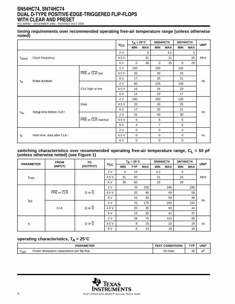
SN54HC74, SN74HC74DUAL D-TYPE POSITIVE-EDGE-TRIGGERED FLIP-FLOPSWITH CLEAR AND PRESET
SCLS094D – DECEMBER 1982 – REVISED JULY 2003
4 POST OFFICE BOX 655303 • DALLAS, TEXAS 75265
timing requirements over recommended operating free-air temperature range (unless otherwisenoted)
VCCTA = 25°C SN54HC74 SN74HC74
UNITVCCMIN MAX MIN MAX MIN MAX
UNIT
2 V 6 4.2 5
fclock Clock frequency 4.5 V 31 21 25 MHz
6 V 0 36 0 25 0 29
2 V 100 150 125
PRE or CLR low 4.5 V 20 30 25
t Pulse duration6 V 17 25 21
nstw Pulse duration2 V 80 120 100
ns
CLK high or low 4.5 V 16 24 20
6 V 14 20 17
↑
2 V 100 150 125
↑
Data 4.5 V 20 30 25
t Setup time before CLK↑6 V 17 25 21
nstsu Setup time before CLK↑2 V 25 40 30
ns
PRE or CLR inactive 4.5 V 5 8 6
6 V 4 7 5
↑
2 V 0 0 0
th Hold time, data after CLK↑ 4.5 V 0 0 0 ns
6 V 0 0 0
switching characteristics over recommended operating free-air temperature range, CL = 50 pF(unless otherwise noted) (see Figure 1)
PARAMETERFROM TO
VCCTA = 25°C SN54HC74 SN74HC74
UNITPARAMETER(INPUT) (OUTPUT)
VCCMIN TYP MAX MIN MAX MIN MAX
UNIT
2 V 6 10 4.2 5
fmax 4.5 V 31 50 21 25 MHz
6 V 36 60 25 29
2 V 70 230 345 290
PRE or CLR Q or Q 4.5 V 20 46 69 58
t d6 V 15 39 59 49
nstpd2 V 70 175 250 220
ns
CLK Q or Q 4.5 V 20 35 50 44
6 V 15 30 42 37
2 V 28 75 110 95
tt Q or Q 4.5 V 8 15 22 19 ns
6 V 6 13 19 16
operating characteristics, TA = 25°CPARAMETER TEST CONDITIONS TYP UNIT
Cpd Power dissipation capacitance per flip-flop No load 35 pF

SN54HC74, SN74HC74DUAL D-TYPE POSITIVE-EDGE-TRIGGERED FLIP-FLOPS
WITH CLEAR AND PRESET
SCLS094D – DECEMBER 1982 – REVISED JULY 2003
5POST OFFICE BOX 655303 • DALLAS, TEXAS 75265
PARAMETER MEASUREMENT INFORMATION
VOLTAGE WAVEFORMSSETUP AND HOLD AND INPUT RISE AND FALL TIMES
VOLTAGE WAVEFORMSPULSE DURATIONS
thtsu
50%
50%50%10%10%
90% 90%
VCC
VCC
0 V
0 V
tr tf
ReferenceInput
DataInput
50%High-Level
Pulse 50%VCC
0 V
50% 50%
VCC
0 V
tw
Low-LevelPulse
VOLTAGE WAVEFORMSPROPAGATION DELAY AND OUTPUT TRANSITION TIMES
50%
50%50%10%10%
90% 90%
VCC
VOH
VOL
0 V
tr tf
Input
In-PhaseOutput
50%
tPLH tPHL
50% 50%10% 10%
90%90%VOH
VOLtrtf
tPHL tPLH
Out-of-PhaseOutput
TestPoint
From OutputUnder Test
CL = 50 pF(see Note A)
LOAD CIRCUIT
NOTES: A. CL includes probe and test-fixture capacitance.B. Phase relationships between waveforms were chosen arbitrarily. All input pulses are supplied by generators having the following
characteristics: PRR ≤ 1 MHz, ZO = 50 Ω, tr = 6 ns, tf = 6 ns.C. For clock inputs, fmax is measured when the input duty cycle is 50%.D. The outputs are measured one at a time with one input transition per measurement.E. tPLH and tPHL are the same as tpd.
Figure 1. Load Circuit and Voltage Waveforms


MECHANICAL DATA
MCFP002A – JANUARY 1995 – REVISED FEBRUARY 2002
1POST OFFICE BOX 655303 • DALLAS, TEXAS 75265
W (R-GDFP-F14) CERAMIC DUAL FLATPACK
0.360 (9,14)0.250 (6,35)
87
141
0.235 (5,97)
0.004 (0,10)
0.026 (0,66)
4 Places
0.015 (0,38)
0.045 (1,14)
0.335 (8,51)
0.008 (0,20)
0.045 (1,14)
Base and Seating Plane
0.005 (0,13) MIN
0.019 (0,48)
0.390 (9,91)
0.260 (6,60)
0.080 (2,03)
4040180-2/C 02/02
0.360 (9,14)0.250 (6,35)
0.280 (7,11) MAX
0.050 (1,27)
NOTES: A. All linear dimensions are in inches (millimeters).B. This drawing is subject to change without notice.C. This package can be hermetically sealed with a ceramic lid using glass frit.D. Index point is provided on cap for terminal identification only.E. Falls within MIL STD 1835 GDFP1-F14 and JEDEC MO-092AB

MECHANICAL DATA
MLCC006B – OCTOBER 1996
1POST OFFICE BOX 655303 • DALLAS, TEXAS 75265
FK (S-CQCC-N**) LEADLESS CERAMIC CHIP CARRIER
4040140/D 10/96
28 TERMINAL SHOWN
B
0.358(9,09)
MAX
(11,63)
0.560(14,22)
0.560
0.458
0.858(21,8)
1.063(27,0)
(14,22)
ANO. OF
MINMAX
0.358
0.660
0.761
0.458
0.342(8,69)
MIN
(11,23)
(16,26)0.640
0.739
0.442
(9,09)
(11,63)
(16,76)
0.962
1.165
(23,83)0.938
(28,99)1.141
(24,43)
(29,59)
(19,32)(18,78)
**
20
28
52
44
68
84
0.020 (0,51)
TERMINALS
0.080 (2,03)0.064 (1,63)
(7,80)0.307
(10,31)0.406
(12,58)0.495
(12,58)0.495
(21,6)0.850
(26,6)1.047
0.045 (1,14)
0.045 (1,14)0.035 (0,89)
0.035 (0,89)
0.010 (0,25)
121314151618 17
11
10
8
9
7
5
432
0.020 (0,51)0.010 (0,25)
6
12826 27
19
21B SQ
A SQ22
23
24
25
20
0.055 (1,40)0.045 (1,14)
0.028 (0,71)0.022 (0,54)
0.050 (1,27)
NOTES: A. All linear dimensions are in inches (millimeters).B. This drawing is subject to change without notice.C. This package can be hermetically sealed with a metal lid.D. The terminals are gold plated.E. Falls within JEDEC MS-004

MPDI002C – JANUARY 1995 – REVISED DECEMBER 20002
1POST OFFICE BOX 655303 • DALLAS, TEXAS 75265
N (R-PDIP-T**) PLASTIC DUAL-IN-LINE PACKAGE
BB AC AD
0.325 (8,26)0.300 (7,62)
0.010 (0,25) NOM
Gauge Plane
0.015 (0,38)
0.430 (10,92) MAX
20
1.060(26,92)
0.940(23,88)
18
0.920
0.850
14
0.775
0.745
(19,69)
(18,92)
16
0.775(19,69)
(18,92)0.745
A MIN
DIM
A MAX
PINS **
(23,37)
(21,59)
Seating Plane
14/18 PIN ONLY20 pin vendor option
4040049/E 12/2002
9
80.070 (1,78)
A
0.045 (1,14)0.020 (0,51) MIN
16
1
0.015 (0,38)0.021 (0,53)
0.200 (5,08) MAX
0.125 (3,18) MIN
0.240 (6,10)0.260 (6,60)
M0.010 (0,25)
0.100 (2,54)
16 PINS SHOWN
MS-100VARIATION
AAC
D
D
D0.030 (0,76)
0.045 (1,14)
NOTES: A. All linear dimensions are in inches (millimeters).B. This drawing is subject to change without notice.
C. Falls within JEDEC MS-001, except 18 and 20 pin minimum body lrngth (Dim A).
D. The 20 pin end lead shoulder width is a vendor option, either half or full width.

MECHANICAL DATA
MSOI002B – JANUARY 1995 – REVISED SEPTEMBER 2001
1POST OFFICE BOX 655303 • DALLAS, TEXAS 75265
D (R-PDSO-G**) PLASTIC SMALL-OUTLINE PACKAGE8 PINS SHOWN
8
0.197(5,00)
A MAX
A MIN(4,80)0.189 0.337
(8,55)
(8,75)0.344
14
0.386(9,80)
(10,00)0.394
16DIM
PINS **
4040047/E 09/01
0.069 (1,75) MAX
Seating Plane
0.004 (0,10)0.010 (0,25)
0.010 (0,25)
0.016 (0,40)0.044 (1,12)
0.244 (6,20)0.228 (5,80)
0.020 (0,51)0.014 (0,35)
1 4
8 5
0.150 (3,81)0.157 (4,00)
0.008 (0,20) NOM
0°– 8°
Gage Plane
A
0.004 (0,10)
0.010 (0,25)0.050 (1,27)
NOTES: A. All linear dimensions are in inches (millimeters).B. This drawing is subject to change without notice.C. Body dimensions do not include mold flash or protrusion, not to exceed 0.006 (0,15).D. Falls within JEDEC MS-012


MECHANICAL DATA
MSSO002E – JANUARY 1995 – REVISED DECEMBER 2001
1POST OFFICE BOX 655303 • DALLAS, TEXAS 75265
DB (R-PDSO-G**) PLASTIC SMALL-OUTLINE
4040065 /E 12/01
28 PINS SHOWN
Gage Plane
8,207,40
0,550,95
0,25
38
12,90
12,30
28
10,50
24
8,50
Seating Plane
9,907,90
30
10,50
9,90
0,38
5,605,00
15
0,22
14
A
28
1
2016
6,506,50
14
0,05 MIN
5,905,90
DIM
A MAX
A MIN
PINS **
2,00 MAX
6,90
7,50
0,65 M0,15
0°–8°
0,10
0,090,25
NOTES: A. All linear dimensions are in millimeters.B. This drawing is subject to change without notice.C. Body dimensions do not include mold flash or protrusion not to exceed 0,15.D. Falls within JEDEC MO-150
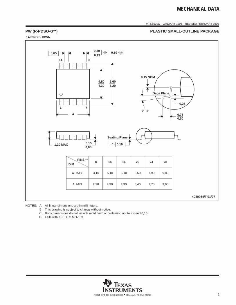
MECHANICAL DATA
MTSS001C – JANUARY 1995 – REVISED FEBRUARY 1999
1POST OFFICE BOX 655303 • DALLAS, TEXAS 75265
PW (R-PDSO-G**) PLASTIC SMALL-OUTLINE PACKAGE14 PINS SHOWN
0,65 M0,10
0,10
0,25
0,500,75
0,15 NOM
Gage Plane
28
9,80
9,60
24
7,90
7,70
2016
6,60
6,40
4040064/F 01/97
0,30
6,606,20
8
0,19
4,304,50
7
0,15
14
A
1
1,20 MAX
14
5,10
4,90
8
3,10
2,90
A MAX
A MIN
DIMPINS **
0,05
4,90
5,10
Seating Plane
0°–8°
NOTES: A. All linear dimensions are in millimeters.B. This drawing is subject to change without notice.C. Body dimensions do not include mold flash or protrusion not to exceed 0,15.D. Falls within JEDEC MO-153

IMPORTANT NOTICE
Texas Instruments Incorporated and its subsidiaries (TI) reserve the right to make corrections, modifications,enhancements, improvements, and other changes to its products and services at any time and to discontinueany product or service without notice. Customers should obtain the latest relevant information before placingorders and should verify that such information is current and complete. All products are sold subject to TI’s termsand conditions of sale supplied at the time of order acknowledgment.
TI warrants performance of its hardware products to the specifications applicable at the time of sale inaccordance with TI’s standard warranty. Testing and other quality control techniques are used to the extent TIdeems necessary to support this warranty. Except where mandated by government requirements, testing of allparameters of each product is not necessarily performed.
TI assumes no liability for applications assistance or customer product design. Customers are responsible fortheir products and applications using TI components. To minimize the risks associated with customer productsand applications, customers should provide adequate design and operating safeguards.
TI does not warrant or represent that any license, either express or implied, is granted under any TI patent right,copyright, mask work right, or other TI intellectual property right relating to any combination, machine, or processin which TI products or services are used. Information published by TI regarding third-party products or servicesdoes not constitute a license from TI to use such products or services or a warranty or endorsement thereof.Use of such information may require a license from a third party under the patents or other intellectual propertyof the third party, or a license from TI under the patents or other intellectual property of TI.
Reproduction of information in TI data books or data sheets is permissible only if reproduction is withoutalteration and is accompanied by all associated warranties, conditions, limitations, and notices. Reproductionof this information with alteration is an unfair and deceptive business practice. TI is not responsible or liable forsuch altered documentation.
Resale of TI products or services with statements different from or beyond the parameters stated by TI for thatproduct or service voids all express and any implied warranties for the associated TI product or service andis an unfair and deceptive business practice. TI is not responsible or liable for any such statements.
Following are URLs where you can obtain information on other Texas Instruments products and applicationsolutions:
Products Applications
Amplifiers amplifier.ti.com Audio www.ti.com/audio
Data Converters dataconverter.ti.com Automotive www.ti.com/automotive
DSP dsp.ti.com Broadband www.ti.com/broadband
Interface interface.ti.com Digital Control www.ti.com/digitalcontrol
Logic logic.ti.com Military www.ti.com/military
Power Mgmt power.ti.com Optical Networking www.ti.com/opticalnetwork
Microcontrollers microcontroller.ti.com Security www.ti.com/security
Telephony www.ti.com/telephony
Video & Imaging www.ti.com/video
Wireless www.ti.com/wireless
Mailing Address: Texas Instruments
Post Office Box 655303 Dallas, Texas 75265
Copyright 2003, Texas Instruments Incorporated