cite this as: j. zuo, a. erbe: physical chemistry …...cite this as: j. zuo, a. erbe: physical...
TRANSCRIPT

Cite this as:
J. Zuo, A. Erbe: Physical Chemistry Chemical Physics, 12, 11467-11476 (2010).
Final copy-edited version of the manuscript is available from:
http://dx.doi.org/10.1039/C004532B
PRIVILEGED DOCUMENT FOR REVIEW PURPOSES ONLY
CREATED USING THE RSC ARTICLE TEMPLATE (VER. 3.1) - SEE WWW.RSC.ORG/ELECTRONICFILES FOR DETAILS
ARTICLE TYPE www.rsc.org/xxxxxx | XXXXXXXX
Optical and electronic properties of native zinc oxide films on
polycrystalline Zn
Juan Zuo,a,b and Andreas Erbe*a
Received (in XXX, XXX) Xth XXXXXXXXX 200X, Accepted Xth XXXXXXXXX 200X
First published on the web Xth XXXXXXXXX 200X
DOI: 10.1039/b000000x
The oxide layer spontaneously formed on zinc and its electrochemically reduced version has been
characterised by a combination of X-ray photoelectron spectroscopy (XPS) and spectroscopic
ellipsometry (SE). The onset of the main electronic absorption, which is directly related to the
bandgap, is extracted from the SE measurements. The SE results are compared with simulations on
the basis of zinc and bulk zinc oxide optical constant data. Measurements in the ultraviolet and
visible (UV/VIS) spectral range show the presence of an absorption ~1.8 eV (680 nm) which is
unaccounted for from the bulk data, and is likely to originate from intragap energy levels,
implicate the presence of surface defects in the layers. Analysis of the Zn LMM Auger peaks in
XPS data show the presence of Zn different from bulk zinc and bulk ZnO, attributed to excess Zn
in the oxide films. Mid-infrared (IR) ellipsometry shows two peaks around 0.12 and 0.15 eV (1000
and 1200 cm-1), which strengthen the assumption of the presence of surface defects in the oxide
layers. Electrochemically reduced samples show a much thinner oxide layer and higher Zn-doping
concentration films than samples purely dipped in NaOH solution. Using a self-contained multiple
sample SE analysis, estimates of the refractive index and absorption coefficient (i.e., the optical
constants) of the oxide films are presented from 1.5 - 4.4 eV (280 to 810 nm).
1 Introduction
Zinc is the fourth most extensively used metal in worldwide production and consumption.1 Films of zinc oxide readily form on the surface of Zn metal, e.g. on galvanized steel under atmospheric conditions. The optical, acid–base properties and electronic properties of such films play a crucial role in their application for corrosion protection.1-5
Because of its frequent application on the outside of the metallic part of materials, its adhesion properties are of crucial importance for any further processing, including the application of protective coatings. The adhesion strength of any material on the zinc crucially depends on non-covalent interactions, and a thorough calculation of adhesion properties involves summing over all possible excitation energies, which are "encoded" in the macroscopic dielectric function of the materials.6 On the other hand, the protection of zinc against corrosion depends e.g. on the conductivity of the oxide layers, which is also manifested in its electronic properties. The oxide layer naturally formed on zinc, as opposed to many other metals, do not form a passive film. Rather, under ambient conditions, a complex chemistry leads to constant increase in the thickness of the oxide layer. Bulk zinc oxide has also enjoyed popularity research in recent years due to its properties as a semiconductor.7, 8 Systematic investigations of the chemistry, optical and electrical properties of the Zn oxide films spontaneously forming on zinc metal are, however, still missing.
In general, the naturally spontaneously formed oxide films are in the range of few nanometer thick for fresh Zn metal. Frequently, the band structure of semiconductors is studied by photoluminescence, which is, however, usually strongly
quenched near metals.9, 10 On the other hand, spectroscopic ellipsometry (SE) is frequently applied in semiconductor research and has been used to determine the optical constants of the natural silicon dioxide film on silicon.11 In this work, SE is used to analyse the native oxide on zinc aiming at an estimate of the optical constants of these films, which are related to the band structure. Because of the differences in the dielectric function of Zn metal and oxide semiconductor, SE is sensitive to these thin films. The dielectric function in the ultraviolet to visible (UV-Vis) and mid-infrared (IR) range is changing from the bulk (Zn) to ambient (air) value across the oxide-containing surface.
SE has previously been performed to determine optical constants of bulk ZnO and its crystalline films. Dispersion models such as the Cauchy12 or Cauchy-Urbach13 models have been used to model the spectra at energies below the bandgap, while a point-by-point fit was used above the band gap12. The optical constants of amorphous ZnO thin films deposited on a silicon (100) substrate by a filtered cathodic vacuum arc technique from 1.13 to 4.96 eV were reported by Khoshman.13
The optical constants of epitaxial ZnO films on sapphire prepared by rf magnetron sputtering and pulsed laser deposition has been extracted by Washington14 and Postava.15
A free excitonic structure located at the band edge was observed and modeled.14 The optical functions of uniaxial ZnO have been reported using two-modulator generalized ellipsometry from 1.45 to 5 eV.16 The resulting band gaps for bulk ZnO as well as crystalline and amorphous films are ~3.4 eV. Furthermore, at energies below the band gap, zero or very low absorption coefficients were obtained. Infrared optical constants from 0.037 to 0.149 eV (300-1200 cm-1) and phonon models of high quality, single crystal wurtzite ZnO films
This journal is © The Royal Society of Chemistry [year] Journal Name , [year], [vol] , 00–00 | 1
5
10
15
20
25
30
35
40
45
50
55
60
65
70
75
80

PRIVILEGED DOCUMENT FOR REVIEW PURPOSES ONLY
CREATED USING THE RSC ARTICLE TEMPLATE (VER. 3.0) - SEE WWW.RSC.ORG/ELECTRONICFILES FOR DETAILS
ARTICLE TYPE www.rsc.org/xxxxxx | XXXXXXXX
prepared by pulsed-laser deposition were also reported.17 In this work, two types of preparation methods were used to
obtain the native zinc oxide films on polycrystalline Zn. In the first, freshly polished pure Zn is dipped in NaOH solution, the other is electrochemical reduced Zn after polished. Those two types of samples were analyzed simultaneously with a self-contained multiple sample analysis.18-20 From there, the optical constants of the native oxide films have been estimated in the UV/Vis range from 280 to 810 nm (1.5 - 4.4 eV) and in the IR range from 440 cm-1 to 6500 cm-1 (0.054 - 0.81 eV). While deriving optical constants of the oxide layers, the optical constants of Zn substrate are refined to give effective, average values for polycrystalline zinc. In order to obtain structural insight into the spontaneously formed oxide films, these investigations were combined with X-ray photoelectron spectroscopy (XPS).
2 Experimental
Sample preparation
Zn foil (99.95% Goodfellow) was cut into pieces of 20×25 cm2 size. These samples were mechanically polished with wet SiC paper up to 4000 grit. After the samples were rinsed with deionized water they were further mechanically polished with 6, 3 and1 µm diamond paste and a final polishing suspension (0.1 µm SiO2, pH=9) to obtain a minimum surface roughness. After that, these samples were sonicated in ethanol for 15 minutes, rinsed with ethanol and dried with nitrogen. These samples were then dipped into 1 M NaOH solution for 2 minutes and then sonicated for 5 minutes in deionized water. After this procedure, the samples should be clean from salts (especially carbonates) and covered with thin layer of native oxide.21 This kind of preparation technique is referred to as method A throughout this work. The samples prepared by the technique referred to as method B were polished in the same way as described previously, but then reduced at -1.1 V in a 2 electrode configuration against a Zn sheet electrode in 1 M Na2CO3 solution for 10 minutes to reduce the surface oxide.22
After that, the samples were also dipped into 1 M NaOH solution for 2 minutes and then sonicated for 5 minutes in deionized water. In each method, at least 3 samples were prepared to check the repeatability of results.
Measurements
UV-Vis spectroscopic ellipsometry
SE was performed at a UV-Vis spectroscopic ellipsometer (SE 800, Sentech, Germany) working in the wavelength range 280 nm-810 nm (1.5 - 4.4 eV). Measurements at different angles of incidence (50o, 60o, 70o and 80o) were performed in order to increase the number of measurements per sample at the same number or unknown parameters. At one angle of incidence, the total number of unknowns is 2N+1, that is the real and imaginary parts of the refractive index n and k at N
wavelengths and the thickness d. However, the total number of measured values is 2N, which are N pairs of the ellipsometric angles ψ and Δ. In addition to the unknowns noise is inherently present in the measurements. Therefore, the measurement at different angles increase the level of
overdetermination of the system, while the use of parameterized dispersion relations decreases significantly the number of unknowns for the optical constants. Furthermore, the sensitivity to the presence of overlayers is different at different angles of incidence: there is a larger sensitivity to layers near the quasi-Brewster angle, though the sensitivity differences are small for metallic substrates as employed here.Mid-infrared spectroscopic ellipsometry
IR spectroscopic ellipsometry was performed in the range 440 cm-1 to 6500 cm-1 (0.054 - 0.81 eV) The apparatus was an IR spectrometer Biorad (Varian) FTS3000 combined with a Sentech SENDIRA variable angle unit (Sentech Instruments, Germany).X-ray photoelectron spectra
X-ray photoelectron spectra (XPS, Quantum 2000, Physical Electronics, USA.) at a take-off angle 54o were obtained using a monochromatic Al Kα source (hν = 1486.6 eV) at pass energy of 23.5 eV. The energy resolution used was 0.2 eV. Depth profiles were obtained by sputtering at a voltage of 1 kV with a current of 2 µA for 0.14 minutes at each sputter interval. This power corresponds to a sputtering rate of 2.16 nm min-1 for Si according to the calibration with standard sample of SiO2 layer on Si. Because an exact calibration of the sputtering rate - depth correspondence in zinc with a complex oxide overlayer is difficult, all sputter depths in this work are given as corresponding to silicon.
Zn LMM Auger peaks were recorded at a take-off angle of 10o to limit the escape depth of photoelectrons. The Zno
reference sample to measure the Zn LMM Auger peaks is polycrystalline zinc after etching till the O1s peak disappears. The Zn2+ reference sample is a single crystal of ZnO (0001) (MaTeck GmbH, Germany) after etching till the C1s peak disappears.
Modelling of the ellipsometric experiments
Structure of stratification
Standard spectroscopic ellipsometry determines the ratio ρ=rp/rs=tan(ψ)exp(iΔ), where rp and rs are the complex amplitude reflection coefficients for light polarized parallel (p) and perpendicular (s) to the plane of incidence. Measured parameters are ψ and Δ. The measured data depend on the complex refractive index m = n + i k of the substrate and all layers, as well as the thicknesses d of all overlayers that may be present. As usual, i= −1 . The complex refractive index is a function of wavelength (or energy), and for nonmagnetic materials as used here related to the dielectric function as ε=m2 .
Real surfaces show a certain roughness, which will in general also affect the polarisation of the reflected light and therefore the ellipsometric parameters. The roughness of the surfaces used in this work was lower than wavelength/10, leading only to ultra-small angle scattering of light. In this regime, the usual approximation of analysing only the first reflected diffraction order should hold, and was used in the data analysis here.
In order to model the experimentally obtained data, an air-oxide film-substrate model is considered in this work.
2 | Journal Name , [year], [vol], 00–00 This journal is © The Royal Society of Chemistry [year]
5
10
15
20
25
30
35
40
45
50
55
60
65
70
75
80
85
90
95
100
105
110

PRIVILEGED DOCUMENT FOR REVIEW PURPOSES ONLY
CREATED USING THE RSC ARTICLE TEMPLATE (VER. 3.1) - SEE WWW.RSC.ORG/ELECTRONICFILES FOR DETAILS
ARTICLE TYPE www.rsc.org/xxxxxx | XXXXXXXX
Including additional transition layers brings more complexity and its inclusion in the data analysis doesn’t improve the fit quality.11, 18
A multi-sample analysis method was employed. Here, the optical constants for the zinc substrates of samples prepared by both methods were allowed to vary in a coupled manner, while the optical constants for the oxide overlayers were varied independently for both samples. This was done after the parameters for the overlayer have been established in previous fits of the overlayer data to yield refined optical constants for pure zinc. A number of models for the dispersion relation of the zinc oxide and the zinc substrate have been tried in the data analysis, as exemplified in Fig. 1. For the ellipsometric data in the UV/Vis range, a Drude-Lorentz model for the zinc substrates was used (fit #1 and #2).23 A Tauc-Lorentz model (fit #1) and a critical point model (fit #2) for the zinc oxide layers were employed, respectively. The second way of analysing the ellipsometric data is based on using independent pairs of the optical constants at every wavelength24, i.e. a wavelength-by-wavelength fit as shown for the oxide layer in fit #3 and #4. In this approach, the optical constants of zinc from fit #1 and #2 kept invariable. The initial optical constants for zinc oxide and zinc as wavelength-by-wavelength lists were taken from fit #1 and #2. In order to use this point-by-point fitting approach for the material in one layer, the thickness of that layer and the optical constants of all other layers need to be known. Therefore, this approach must be followed with great caution. For the ellipsometric data analysis in the mid-IR range, a Drude-Lorentz model for the zinc substrates and zinc oxide
layers were employed as shown in fit #5, while the thickness of oxide layers were taken from the UV/Vis data analysis.
The different models used in this work and their respective physical meaning are discussed in the following.Drude-Lorentz model
The optical constants of zinc were modelled with the combination of the well-known Drude and Lorentz models.25
=DrudeLorentz
=∞−P
2
2i∑
l=1
N P
2
o
2−2−i
Here, ωp and ω τ are the plasma frequency and damping term, respectively, of the free electrons, while Ωp is related to the oscillator strength of a harmonic oscillator with a resonance frequency of Ωo and a damping constant of Ωτ . The total numbers of oscillators is N, and ω is the frequency of incident light.Tauc-Lorentz model
This model is used to parameterize the imaginary part ε2 of the dielectric function optical constants of amorphous materials based on an ideally simple interband structure.26-28
The real part ε1 is obtained through the Kramers-Krönig relation. In the following equation, Θl(E) = 0 when E≤ Eg,l and Θl(E)= 1 when E> Eg,l.
2E =∑l=1
l=N Al E 0,l C l E−E g ,l2
E2−E0, l
2 2C l
2E
2
1El E
1E =1∞2
P∫0
∞ x2x
x2−E
2d x
Here Eg,l is the band gap and Eo,l is the peak in the joint density of states of the respective absorption, Cl is the broadening parameter and Al is a prefactor. The Tauc-Lorentz model is usually used for one absorption (N=1) only. For reasons which become apparent in the results section, we use a case with N=2 for one set of samplesCritical point model
This model describes the dielectric functions of native oxide layers and has been successfully used to model native or electrochemically grown oxide layers on the compound semiconductors GaP, GaAs, GaSb, InP, InAs and InSb in the UV/Vis range.29
E =ab E−∑l=1
l=N
An
ei l
E−E g , li lHere a and b are complex parameters, A is the amplitude, Eg,l
is threshold energy of the l-th critical point, while Γl is broadening parameter of the critical point. The phase angle φl
is introduced to account for excitonic effects or other inaccuracies of the model.29
3 Results and discussion
This journal is © The Royal Society of Chemistry [year] Journal Name , [year], [vol] , 00–00 | 3
Fig. 1 Models of the stratification used to analyse the spectroscopic ellipsometry data in the UV/Vis (a) fit #1, (b) fit #2, (c) fit #3, (d) fit
#4, and in the IR range (e) fit #5.
air
Zn Drude-Lorentz model fit model parameters
Tauc-Lorentz model fit d and model parameters
(a) Fit #1
air
Zn Drude-Lorentz model fit model parameters
critical point model fit d and model parameters
(b) Fit #2
air
Zn Tabulated from fit #1
fit d and n, k at each λ
(c) Fit #3
air
Zn Tabulated from fit #2
fit d and n, k at each λ
(d) Fit #4
air
Zn Drude-Lorentz model fit model parameters
Drude-Lorentz model fit model parameters
(e) Fit #5
5
10
15
20
25
30
35
40
45
50
55
60
65
70
75

PRIVILEGED DOCUMENT FOR REVIEW PURPOSES ONLY
CREATED USING THE RSC ARTICLE TEMPLATE (VER. 3.0) - SEE WWW.RSC.ORG/ELECTRONICFILES FOR DETAILS
ARTICLE TYPE www.rsc.org/xxxxxx | XXXXXXXX
Fig. 2 Depth profiles of zinc oxide layers on Zn of samples prepared by method A (a) and method B (b) determined by XPS.
X-ray photoelectron spectroscopy
Depth profiles of samples prepared by methods A and B were obtained by combining a sequence of Ar ion gun etch cycles interleaved with XPS measurements from the freshly exposed surface. XPS high resolution spectra were acquired at every interval after etching. The spectra provide the means of analyzing the composition of these surfaces. Figure 2 (a) and (b) give the plots of atomic concentration of C1s, O1s and Zn2p as function of depth in nm. The actual depth for each XPS analysis is dependent on the etch-rate of the ion-gun to elements. The depth is based on the calibration of the etching time - depth correlation on a standard sample of SiO2 on a Si wafer. This calibration does not directly apply to Zn with oxide layers, however, an exact calibration on the low length scales used for analysis here in a material of complex composition is difficult, and has not been undertaken. As can be seen from Figure 2, there was a small amount of carbon on the initial surface for samples prepared by method A and B, but it was undetectable after removal of a few Ångström of material. Samples by method B after 10 days exposed to air showed C1s signals even after removal of a few nm of
material. This indicates the initially observed native oxide layers on Zn of samples prepared by both methods are not zinc carbonate, but the inevitable carbon-containing contaminants after exposure to ambient conditions.
Fig. 3 Zn LMM Auger peaks in different depths of samples prepared by method A (a) and B (b) compared with Zno and Zn2+ references.
Charge effects and oxygen desorption due to the ion etching may change the atomic composition during the measurement process.30 However, qualitative information about the thickness of the zinc oxide on samples prepared by different methods can be obtained. The oxygen concentration decreased to zero at 2-3 nm depth for method B compared to 12-14 nm depth for method A. This demonstrates that the oxide film prepared by method B is much thinner than the one by method A.
The Zn 2p3/2 peaks of Zn0 and Zn2+ (e.g. ZnO) at binding energies of 1021.8 eV31 and 1022.5 eV31 or 1021.8 eV32, which depends on different preparation methods, are too close to differentiate the two species. Therefore, the Zn LMM Auger peaks were measured at every interval. The effective analysis
4 | Journal Name , [year], [vol], 00–00 This journal is © The Royal Society of Chemistry [year]
5
10
15
20
25
30
35
40
45
PRIVILEGED DOCUMENT FOR REVIEW PURPOSES ONLY
CREATED USING THE RSC ARTICLE TEMPLATE (VER. 3.1) - SEE WWW.RSC.ORG/ELECTRONICFILES FOR DETAILS
ARTICLE TYPE www.rsc.org/xxxxxx | XXXXXXXX
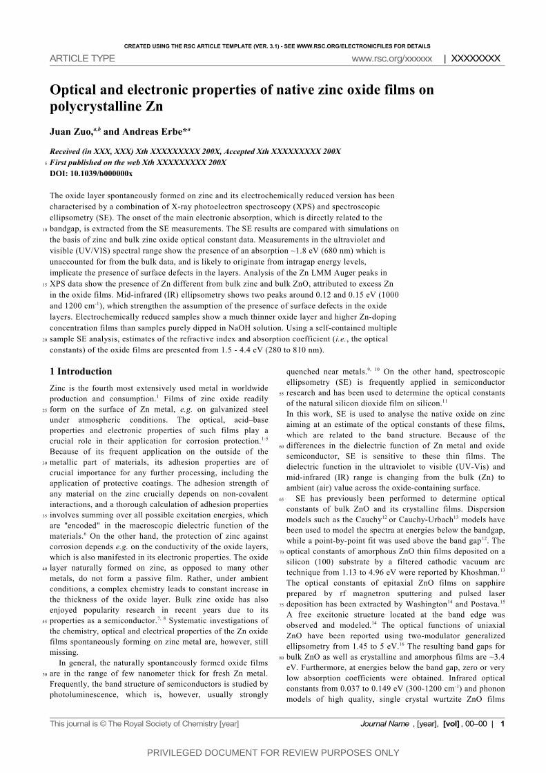
depth d depends on the inelastic mean free path λ of the electrons in Zn at the Zn LMM kinetic energy, and the angle θ between the sample surface and analyzer input lens. It is given as33 d = 3 λ sin θ . Here, θ= 10o , and λ ≈ 1.7 nm were used.34 Thus, d ≈ 0.9 nm was obtained and the etched thickness every interval was chosen more than 0.9 nm, e.g. 1.2 nm. The changes of the Zn LMM peak at different depths from the surface are shown in Figure 3. These peaks are compared to Zn LMM of Zno and Zn2+ references. The Zn LMM of Zn0 is in the range of 985-988 eV, while for Zn2+ it is in the region between 992 and 995 eV. For both methods, there is Zn2+ on the surface of the samples, the fraction of which decreased gradually with depth. Zn0 exists in the oxide
Fig. 4 Zn2+ atomic concentration (Zn2+/(Zno+Zn2+)) vs depth for samples prepared by method A and B.
overlayer in both samples till it reaches 100% in the bulk. Zn2+
atomic concentrations in samples prepared by both methods in the oxide can be obtained by decomposing the Zn LMM peak into its Zn2+ and Zn0 contributions and comparing the corresponding area. This method provides pseudo-quantitative information concerning Zn Auger peaks for various ratios of Zno to Zn2+ through the oxide layer.30, 35, 36
In Figure 4, the Zn2+ atomic concentration, calculated as Zn2+/(Zno+Zn2+) is depicted as function of depth in nm. There is 100% Zn2+ on the surface of samples prepared by method A, instead of the coexistence of Zn2+ and Zn0 on the surface of samples prepared by method B. The slopes of the two curves are quite different as well. The Zn2+ atomic concentration decreased to zero just after ~3.5 nm for method B but after ~14 nm for method A. The metallic state Zn0 after Ar plasma treatment could exist due to charging effects or oxygen desorption during the plasma treatment, however the presence of Zn0 on the surface of samples prepared by method B exclude the possibility that this metallic Zn is only present due to reduction of Zn2+
by the Ar plasma.
UV-Vis spectroscopic ellipsometry
The XPS results show a graded transition of concentration across the interface. However, such a gradual transition is always detected in the experiment, even if the real transition is
much sharper, because of the non-zero depth resolution of the electron spectroscopic techniques. For optical experiments, the relation between effective average and actual spatial dependent optical functions has been considered in many works.37, 38 Briefly, the spatial dependent optical constants can be replaced by a spatial average one if the region is sufficiently thin. The effective optical constants obtained by spectroscopic ellipsometry fitted by simple three phase model can be taken to be the simple spatial average of the actual variation.
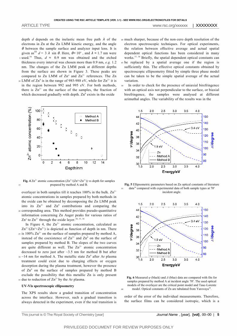
In order to check for the presence of uniaxial birefringence with an optical axis not perpendicular to the surface, or biaxial birefringence, the samples were analysed at different azimuthal angles. The variability of the results was in the
Fig. 5 Ellipsometric parameters based on Zn optical constants of literature data39 compared with experimental data of both sample types at 70o
incident angle.
Fig. 6 Measured ψ (black) and Δ (blue) data are compared with fits for samples prepared by method A at incident angle 70o. The used optical models of the overlayer are the critical point model and Tauc-Lorentz
model. Optical constants of Zn are tabulated from Yarovaya39.
order of the error of the individual measurements. Therefore, the surface films can be considered isotropic, which is a
This journal is © The Royal Society of Chemistry [year] Journal Name , [year], [vol] , 00–00 | 5
5
10
15
20
25
30
35
40
45
50
55
60

PRIVILEGED DOCUMENT FOR REVIEW PURPOSES ONLY
CREATED USING THE RSC ARTICLE TEMPLATE (VER. 3.0) - SEE WWW.RSC.ORG/ELECTRONICFILES FOR DETAILS
ARTICLE TYPE www.rsc.org/xxxxxx | XXXXXXXX
typical characteristics of few nanometre thick, spontaneously formed films.
The optical constants of single crystalline Zn (0001)39 were used to calculate the ellipsometric parameters ψ and Δ using home-made codes (reflcalc) based on optical multilayer theory.40, 41, 42 These ψ and Δ were depicted in Figure 5 and compared with the experimental data of samples prepared by method A and B. Compared with the curves based on Zn literature data as displayed in Figure 5, both experimental curves are clearly shifted. Furthermore, the experimental ψ
and Δ curves of samples prepared by method A bend around 1.9 and 3.4 eV. The weaker feature at 1.9 eV is observed in samples prepared by method B, but none is visible at 3.4 eV. The general differences in the curves to the curves of pure Zn are attributed to the presence of the oxide layer. Both "dips" in the ψ curves indicate the existence of a rapid change of the
Fig. 7 Optical constants of zinc from literature39 and in this work from fit #1 and fit #2.
Table 1 Fit results for the thickness of the zinc oxide films using the respective models.
MethodTauc-Lorentz model
fit #1Critical point model
fit #2A 13.0± 0.7 nm 10.4± 0.6 nmB 1.8± 0.3 nm 1.4± 0.2 nm
optical functions at such wavelengths, like the onset of a strong absorption.
The differences in the region lower than 1.9 eV could not be explained by any model for the overlayer, though many different models have been used, ranging from simple Cauchy and Sellmeier dispersion over the Tauc-Lorentz model to the critical point model. This layer is supposed to be no absorbing at such low energy. Even the inclusion of the possibility of mixtures of Zn and oxides in the overlayer cannot quantitatively explain the difference. The disagreement in the range always exist no matter which model is used. Figure 6 selectively shows the measured ψ and Δ data and the fits of sample A at incident angle 70o. The used optical models of the zinc oxide overlayers are the critical point model and the
Tauc-Lorentz model. The differences in the region lower than 1.9 eV in Fig. 6 are clearly visible. Keeping the substrate optical constants fixed at the tabulated values and fitting the overlayer data on a point-by-point basis does not lead to physical results. The substrate reference data was not sufficient to explain the results here. Therefore, the substrate parameters were coupled for the samples prepared by two methods, and the multisample analysis method was used to analyse the data, as mentioned in the experimental sections. This disagreement is expected since the tabulated optical constant of Zn is from a single crystal and not from polycrystalline material, though Yarovaya et al.39 conclude that zinc can effectively regarded as optically isotropic material in the visible region. The difference in density and microstructure may have an effect.
Therefore, zinc was set up variable and modelled by a Drude-Lorentz model. The overlayers of the two kinds of samples were modelled using the Tauc-Lorentz model and the
Table 2 Parameters of the the Drude Lorentz model for zinc resulting from the modelling fit #1 and fit #2.
ωp ωτ Ωo Ωp Ωτ
Fit #1 64814± 17 3965± 8 13980± 1 72933± 14 8490± 1
Fit #2 56750± 20 2911± 9 13521± 1 76861± 16 9808± 1
critical point model. For the samples prepared by method A, two Tauc-Lorentz oscillators (fit #1) or two critical points (fit #2) were used to describe the dispersion relation of the zinc oxide overlayer. The parameters of the Drude-Lorentz model for the zinc substrate were varied simultaneously. For the samples prepared by method B, one Tauc-Lorentz oscillator (fit #1), one critical point (fit #2) were used for the overlayer, and the same parameters for the zinc as mentioned before. Table 1 lists the fitted thickness of the zinc oxide films of the respective models.
Table 2 lists the parameters of the Drude-Lorentz model of zinc resulting from the modelling in fit #1 and fit #2. Figure 7 compares the optical constants of zinc from literature39 and obtained in this work from fit #1 and fit #2. The curves obtained by fitting match well in the high energy range and differ in the lower energy region. Especially the absorption coefficients are quite different at photon energies lower than 1.77 eV. Fit #3 and #4 used the optical constants of Zn from fit #1 and #2 and kept the thickness of overlayers constant. Point by point model is used to fit the optical constants of overlayers for sample A and B. The improved fit qualities of these two fits might indicate some inflexibility of the used two models. However, the better fit qualities might be also achieved by the unphysical optical constants, since the Kramers-Krönig consistency is not enforced.18, 19, 24
Figure 8 shows the optical constants of the zinc oxide layers of samples prepared by method A and B. Table 3 lists the parameters of the overlayers prepared by method A and B resulting from fit #2. For method A, the critical point model produces a 0.1-0.2 higher refractive index but around 3 nm lower thickness of overlayers. This might be due to the internal correlation of the optical constants and thickness of
6 | Journal Name , [year], [vol], 00–00 This journal is © The Royal Society of Chemistry [year]
5
10
15
20
25
30
35
40
45
50
55
60
65
70
75
80
85

PRIVILEGED DOCUMENT FOR REVIEW PURPOSES ONLY
CREATED USING THE RSC ARTICLE TEMPLATE (VER. 3.1) - SEE WWW.RSC.ORG/ELECTRONICFILES FOR DETAILS
ARTICLE TYPE www.rsc.org/xxxxxx | XXXXXXXX
overlayers. On metallic substrates, especially the correlation between thickness and the imaginary part of the refractive index is hard to overcome. Point by point fits (fit #3 and #4) in principle produce similar optical constants to their respective initial ones (fit #1 and #2), which is not surprising because the fit data by this model mostly depends on the initially used tabulated data. In Figure 8 (b), the absorption coefficient shows two characteristic peaks around 3.1 and 1.8 eV due to the semiconductor and degenerate semiconductor
absorption (discussed in the following section). Compared with method A, the fit results of sample B show characteristic differences between the different models used, especially the real part of the refractive index. The reason might be the strong correlation of the optical constants and thickness results in the uncertainty of optical constants since method B produces only a 1-2 nm thick layer on the surface. The presence of roughness could produce erroneous results, but
Fig. 8 Optical constants in UV/Vis range of zinc oxide layers on Zn for method A, (a) refractive index, (b) absorption coefficient, and method B (c) refractive index, (d) absorption coefficient. In every figure, corresponding optical constants of pure ZnO taken from literature14 were shown as well.
Table 3 Parameters of the overlayers prepared by method A and B resulting from the modelling fit #2. For method A, one critical point is used, while there are two for sample prepared by method B.
Re(a) Im(a) Re(b) Im(b) A0/A1 φ0/φ1 Eg0/Eg1 Γ0/Γ1
Method A 2.5± 0.1 0.6± 0.1 -0.3±0.1 -0.1±0.01 2.1±0.1/0.8±0.1 4.5± 0.1/0.7±0.1 2.9±0. 1/2.2±0.1 1.4±0.1/0.9±0.1Method B 1.6±0.1 −3.8±0.1 -0.8±0.1 1.4±0.1 5.1±0.1 5.2± 0.1 3.3± 0.1 1.2±0.1
not differences in the different models. The refractive index and absorption coefficient for method B are higher than those for method A. They show a larger difference to the ZnO data. The absorption coefficient for method B has only one
semiconductor absorption peak compared to method A, which has two. The typical band gap absorption around 3.4 eV has disappeared for method B.
Considering the models used in the data analysis of
This journal is © The Royal Society of Chemistry [year] Journal Name , [year], [vol] , 00–00 | 7
5
10
15
20
25
30

PRIVILEGED DOCUMENT FOR REVIEW PURPOSES ONLY
CREATED USING THE RSC ARTICLE TEMPLATE (VER. 3.0) - SEE WWW.RSC.ORG/ELECTRONICFILES FOR DETAILS
ARTICLE TYPE www.rsc.org/xxxxxx | XXXXXXXX
spectroscopic ellipsometry, the Tauc-Lorentz model is valid for interband transitions and simply ignores any absorption below the band gap, such as Urbach tail effects, defect absorption and intraband absorption at low energy are not included. In the Figure 8, the absorption coefficient from Tauc-Lorentz model is zero below the bandgap absorption. The critical point model produces better fit quality and yields a non-zero absorption coefficient below the band gap. The accuracy of this model for the description of the optical constants can be also improved if different types of critical point model are considered and the coefficient m of (E-
Eg+iΓ)m can be an adjustable model parameters. The inflexibility of this model was improved by using point-by-point model.
Comparing the results for the thin native oxide films with those of bulk, crystalline ZnO (Figure 8) shows first of all major differences in the real part of the refractive index. This may be due to problems in our analysis technique. The magnitude of the imaginary part of the refractive index might also be disputable, however, its wavelength dependence, i.e.
Fig. 9 Ellipsometric parameters of both type of samples and computations based on Zn literature data of the optical constants. The inset shows a magnification of ψ for the computed data and for samples prepared by
method B.
the energy where it sharply rises associated with the onset of an electronic transition, is independent of the chosen model and the respective fit parameters and can directly be seen in the raw data, e.g. in the plots of ψ vs. wavelength (Figure 5). The literature data in Figure 8 shows a strong excitonic peak around 370 nm (3.35 eV) at room temperature. For such thin, amorphous or at maximum nanocrystalline structures as in the thin films, excitonic absorption are not possible due to the missing long range order. In bulk ZnO, the bandgap is around 3.4 eV, corresponding to absorption at ~365 nm. For method A, the absorption associated with the main band gap of the semiconductor is still clearly visible, though it is shifted to slightly lower energy, indicating a modification of the band gap to lower energies. In addition, a first absorption at much lower energy, around 1.8 eV is seen for method A. This absorption becomes dominant in samples prepared by method B, where the main absorption associated with the band gap
around 3.4 eV is not seen anymore. Though there is considerable variability in the determined results for method B, this qualitative result is there independent of the chosen model.
The feature around 1.8 eV is typical for ZnO with excess Zn which was prepared by exposing to Zn vapour. The related absorption is referred to as β-absorption.43 This presence of excess Zn is also confirmed by our XPS results. The chemical structures of the overlayers in samples prepared by method A and B is therefore a zinc oxide layer with dispersed or dissolved excess zinc. The observed β-absorption is likely a result of the production of lattice defects. The lower energy absorption around 1.8 eV for both samples observed in this work could from intragap energy levels, which in turn implicate the presence of surface defects in the overlayers. According to theoretical work44 on the electronic structure of non-stoichiometric ZnO, interstitial Zn (Zni) produces a shallow donor level at 0.5 eV below the bottom of the conduction band and a defect vacant O (Vo) produces a deep donor level at 1.3 eV below the bottom of conduction band. Comparing this result with our experimental data that the defect absorption level is 1.6 eV below the conduction band (3.4 eV-1.8 eV), the vacant oxygen could be the main factor to induce the intraband absorption. Similar shifts of the absorption onset to higher wavelength have been reported for ZnO where part of the Zn is replaced by other divalent cations.8 One reason for the differences between samples with and without electrochemical reduction could be differences in the presence of hydrogen.45
Mid-Infrared spectroscopic ellipsometry
SE measurements were extended into the IR (440 cm-1 to 6500 cm-1, that is 0.054 eV to 0.81 eV). The measured data are shown in Figure 9. Two characteristic peaks around 0.12 and 0.15 eV (1000 and 1200 cm-1) of ψ and Δ for both preparation methods can be seen. The intensity of the two peaks for method B is much lower than for method A. More obvious visible peaks for method B was shown in the inserted figure of figure 9. To compare the experimental data, the ellipsometric parameters ψ and Δ of Zn films in IR range were calculated with the optical constants of Zn films taken from elsewhere46
using the same method as mentioned before for UV-Vis SE. These ψ and Δ were depicted as dotted line in Figure 9. No peaks are found around 0.12 and 0.15 eV. The general differences between the curves of pure Zn and experiment are certainly attributed to the presence of the oxide overlayer.
Similar to before, multiple sample analysis is used to model experimental data in the mid-IR range. The Drude-Lorentz model with two oscillators was used to model overlayers for both sample types while zinc was set up variable and modeled by a Drude-Lorentz model. Two characteristic curves of optical constants of oxide layers can be obtained in fitting analysis (not shown here). Film and bulk ZnO have the transverse and longitudinal phonon frequency around 0.05 and 0.07 eV respectively.17 The additional vibrational modes at 0.12 and 0.15 eV compared to the pure ZnO are probably due to states induced by the presence of the excess Zn in the oxide layer.
8 | Journal Name , [year], [vol], 00–00 This journal is © The Royal Society of Chemistry [year]
5
10
15
20
25
30
35
40
45
50
55
60
65
70
75
80
85
90
95

PRIVILEGED DOCUMENT FOR REVIEW PURPOSES ONLY
CREATED USING THE RSC ARTICLE TEMPLATE (VER. 3.1) - SEE WWW.RSC.ORG/ELECTRONICFILES FOR DETAILS
ARTICLE TYPE www.rsc.org/xxxxxx | XXXXXXXX
4 Conclusions
XPS sputter profiles and analysis of the Auger LMM peaks provides information about the layer thickness and chemical composition at a certain depth, but the interpretation of the depth profile depends on the calibration of the ion-etch rate, the inelastic mean free path, and the roughness of the surface. Nevertheless, strong evidence for the presence of Zn inside the oxide layer is found. Different models for the interpretation of SE data have been used, and despite the low thickness of the films, features which cannot be explained by the data of the pure components were found. The combination of data from both techniques is crucial to understand the optical and electronic properties of layers spontaneously forming on a material's surface under ambient conditions. Both techniques show the presence of Zn0 inside the native oxide layer on zinc, making it a non-stociometric suboxide type of film. This presence leads to additional absorptions at 1.8 eV, which were observed using spectroscopic ellipsometry. The low energy absorption for both samples observed in this work is likely to originate from intragap energy levels.
The electrochemically reduced samples (Method B) show much less thick layer compared to samples purely dipped in NaOH solution (Method A). At the same time, it also shows higher Zn-doping concentration. Furthermore, the difference of chemical structure resulted in significant differences in the absorption characteristics of the formed zinc suboxide. Supplementary mid-IR SE data shows an additional vibrational mode due to the presence of excess Zn inside the oxide layers. The results obtained here indicate that, in order to model and investigate the adhesion properties of zinc covered with native oxide, the use of single-crystalline bulk ZnO is not sufficient, due to the difference in electronic structure between bulk ZnO and the native oxide films.
The SE results obtained show that the oxide films on zinc show a considerable absorption of visible light at lower energy than the pure oxide. In exposure to atmospheric conditions in the presence of sunlight, excited states can therefore be easily generated, with different wanted or unwanted consequences. They may contribute to the decomposition and deadhesion of coatings. On the other hand, a chemical route to such modified zinc oxide may pave the way for large-scale cheap solar cells on zinc basis.
5 Acknowledgment
We like to thank Bekir Salgin for inspiring this study, as well as Prof. Stratmann for his support.
Notes and references
a Department of Interface Chemistry and Surface Engineering, Max-
Planck-Institut für Eisenforschung GmbH, Düsseldorf, Germany. Fax:
+49 211 6792218; Tel: +49 211 6792890; E-mail: [email protected] Current address: Department of Mechanical Engineering, Xiamen
University of Technology, Xiamen, China. E-mail: [email protected]
1. X. G. Zhang, Corrosion and electrochemistry of zinc, Plenum Press, New York, 1996.
2. M. G. Barthes-Labrousse, G. Ballerini and K. Ogle, Appl. Surf. Sci., 2007, 253, 6860.
3. P. Lang and C. Nogues, Surf. Sci., 2008, 602, 2137.4. A. Najari, P. Lang, P. C. Lacaze and D. Mauer, Prog. Org. Coat.,
2009, 64, 392.5. C. Nogues and P. Lang, Langmuir, 2007, 23, 8385.6. V. A. Parsegian, Van der Waals Forces, Cambridge University Press,
2006.7. A. Janotti and C. G. Van de Walle, Reports on Progress in Physics,
2009, 72.8. H. von Wenckstern, H. Schmidt, M. Brandt, A. Lajn, R. Pickenhain,
M. Lorenz, M. Grundmann, D. M. Hofmann, A. Polity, B. K. Meyer, H. Saal, M. Binnewies, A. Borger, K. D. Becker, V. A. Tikhomirov and K. Jug, Prog. Solid State Chem., 2009, 37, 153.
9. W. Gebauer, A. Langner, M. Schneider, M. Sokolowski and E. Umbach, Physical Review B, 2004, 69.
10. G. Ritchie and E. Burstein, Physical Review B, 1981, 24, 4843.11. Y. Y. Chen and G. Jin, Spectroscopy, 2006, 21, 26.12. Y. C. Liu, J. H. Hsieh and S. K. Tung, Thin Solid Films, 2006, 510,
32.13. J. M. Khoshman and M. E. Kordesch, Thin Solid Films, 2007, 515,
7393.14. P. L. Washington, H. C. Ong, J. Y. Dai and R. P. H. Chang, Appl.
Phys. Lett., 1998, 72, 3261.15. K. Postava, H. Sueki, M. Aoyama, T. Yamaguchi, C. Ino, Y. Igasaki
and M. Horie, J. Appl. Phys., 2000, 87, 7820.16. G. E. Jellison and L. A. Boatner, Physical Review B, 1998, 58, 3586.17. N. Ashkenov, B. N. Mbenkum, C. Bundesmann, V. Riede, M.
Lorenz, D. Spemann, E. M. Kaidashev, A. Kasic, M. Schubert, M. Grundmann, G. Wagner, H. Neumann, V. Darakchieva, H. Arwin and B. Monemar, J. Appl. Phys., 2003, 93, 126.
18. C. M. Herzinger, B. Johs, W. A. McGahan and W. Paulson, Thin
Solid Films, 1998, 313, 281.19. C. M. Herzinger, B. Johs, W. A. McGahan, J. A. Woollam and W.
Paulson, J. Appl. Phys., 1998, 83, 3323.20. K. Jaerrendahl and H. Arwin, Thin Solid Films, 1998, 313-314, 114.21. W. Furbeth and M. Stratmann, Corros. Sci., 2001, 43, 207.22. Z. Mekhalif, L. Massi, F. Guittard, S. Geribaldi and J. Delhalle, Thin
Solid Films, 2002, 405, 186.23. C. F. Bohren and D. Huffman, Scattering and Absorption of Light by
Small Particles, Wiley-VCH, 2004.24. C. M. Herzinger, P. G. Snyder, B. Johs and J. A. Woollam, J. Appl.
Phys., 1995, 77, 1715.25. F. Wooten, Optical Properties of Solids, Academic Press, New York,
1972.26. G. E. Jellison and F. A. Modine, Appl. Phys. Lett., 1996, 69, 2137.27. G. E. Jellison and F. A. Modine, Appl. Phys. Lett., 1996, 69, 371.28. G. E. Jellison, F. A. Modine, P. Doshi and A. Rohatgi, Thin Solid
Films, 1998, 313, 193.29. S. Zollner, Appl. Phys. Lett., 1993, 63, 2523.30. J. F. Wager and C. W. Wilmsen, J. Appl. Phys., 1979, 50, 874.31. J. F. Moulder, W. F. Stickle, P. E. Sobol and K. D. Bomben,
Handbook of X-ray Photoelectron Spectroscopy.32. S. W. Gaarenstroom and N. Winograd, J. Chem. Phys., 1977, 67,
3500.33. Quantum Operator's Guide, Physical Electronic, Inc.34. C. J. Powell and A. Jablonski, NIST Electron Ineleastic-Mean-Free-
Path Database-Version 1.1, National Institute of Standards and Technology, Gaithersburg, MD, 2000.
35. J. S. Johannessen, W. E. Spicer and Y. E. Strausser, Appl. Phys. Lett., 1975, 27, 452.
36. J. S. Johannessen, W. E. Spicer and Y. E. Strausser, J. Appl. Phys., 1976, 47, 3028.
37. D. E. Aspnes and J. B. Theeten, J. Electrochem. Soc., 1980, 127, 1359.
38. W. J. Plieth and K. Naegele, Surf. Sci., 1977, 64, 484.39. R. G. Yarovaya, I. N. Shklyarevskii and E.-S. A. F. A., Sov. Phy.
-JETP, 1974, 38, 331.40. J. Lekner, The theory of reflection, Martinus Nijhoff Publishers,
1987.41. M. Schubert, Physical Review B, 1996, 53, 4265.
This journal is © The Royal Society of Chemistry [year] Journal Name , [year], [vol] , 00–00 | 9
5
10
15
20
25
30
35
40
45
50
55
60
65
70
75
80
85
90
95
100
105
110
115
120
125

PRIVILEGED DOCUMENT FOR REVIEW PURPOSES ONLY
CREATED USING THE RSC ARTICLE TEMPLATE (VER. 3.0) - SEE WWW.RSC.ORG/ELECTRONICFILES FOR DETAILS
ARTICLE TYPE www.rsc.org/xxxxxx | XXXXXXXX
42. http://home.arcor.de/aerbe/en/prog/a/reflcalc.html43. G. Heiland, E. Mollwo and F. Stoeckmann, in Solid state physics,
eds. F. Seitz and D. Turnbull, Academic, New York, 1959, vol. 8.44. P. S. Xu, Y. M. Sun, C. S. Shi, F. Q. Xu and H. B. Pan, Nuclear
Instruments & Methods in Physics Research Section B-Beam
Interactions with Materials and Atoms, 2003, 199, 286.45. S. Chatman, L. Emberley and K. M. Poduska, ACS Applied Materials
& Interfaces, 2009, 1, 2348.46. G. P. Motulevich and A. A. Schubin, Soviet Physics JETP, 1969, 29,
24.
Content Graphics
Description: The native oxide layer formed spontaneously in air on zinc contains excess Zn0
and is therefore absorbing light over a broad range in the visible spectrum.
10 | Journal Name , [year], [vol], 00–00 This journal is © The Royal Society of Chemistry [year]
5
10
15
20
25