cis 501 computer organization and design
TRANSCRIPT

CIS 501 | Dr. Joe Devietti | ISAs & Single Cycle 1
CIS 501Computer Organization and Design
Unit 4: Single-Cycle Datapath
Based on slides by Profs. Benedict Brown, C.J. Taylor, Amir Roth & Milo Martin

CIS 501 | Dr. Joe Devietti | ISAs & Single Cycle 2
This Unit: Single-Cycle Datapath• Overview of ISAs• Datapath storage elements• MIPS Datapath• MIPS Control
CPUMem I/O
System softwareAppApp App
CIS 501 | Dr. Joe Devietti | ISAs & Single Cycle 3
Readings
• P&H• Sections 4.1 – 4.4

Recall from CIS240…
CIS 501 | Dr. Joe Devietti | ISAs & Single Cycle 4

240 Review: ISA
• App/OS are software … execute on hardware• HW/SW interface is ISA (instruction set architecture)
• A “contract” between SW and HW• Encourages compatibility, allows SW/HW to evolve independently• Functional definition of HW storage locations & operations
• Storage locations: registers, memory• Operations: add, multiply, branch, load, store, etc.
• Precise description of how to invoke & access them• Instructions (bit-patterns hardware interprets as commands)
CIS 501 | Dr. Joe Devietti | ISAs & Single Cycle 8
CPUMem I/O
System softwareAppApp App

240 Review: LC4 ISA
• LC4: a toy ISA you know• 16-bit ISA (what does this mean?)• 16-bit insns• 8 registers (integer)• ~30 different insns• Simple OS support
• Assembly language• Human-readable ISA representation
CIS 501 | Dr. Joe Devietti | ISAs & Single Cycle 9
CPUMem I/O
System softwareAppApp App .DATA
array .BLKW #100sum .FILL #0
.CODE
.FALIGNarray_sum
CONST R5, #0LEA R1, arrayLEA R2, sum
array_sum_loopLDR R3, R1, #0LDR R4, R2, #0ADD R4, R3, R4STR R4, R2, #0ADD R1, R1, #1ADD R5, R5, #1CMPI R5, #100BRn array_sum_loop

371/501 Preview: A Real ISA
• MIPS: example of real ISA• 32/64-bit operations• 32-bit insns• 64 registers
• 32 integer, 32 floating point• ~100 different insns• Full OS support
CIS 501 | Dr. Joe Devietti | ISAs & Single Cycle 10
CPUMem I/O
System softwareAppApp App .data
array: .space 100sum: .word 0
.text
array_sum:li $5, 0la $1, arrayla $2, sum
array_sum_loop:lw $3, 0($1)lw $4, 0($2)add $4, $3, $4sw $4, 0($2)addi $1, $1, 1addi $5, $5, 1li $6, 100blt $5, $6, array_sum_loop
Example code is MIPS, but all ISAs are similar at some level

240 Review: Assembly Language
• Assembly language• Human-readable representation
• Machine language• Machine-readable representation
• 1s and 0s (often displayed in “hex”)
• Assembler• Translates assembly to machine
CIS 501 | Dr. Joe Devietti | ISAs & Single Cycle 12
CPUMem I/O
System softwareAppApp App
x9A00 CONST R5, #0x9200 CONST R1, arrayxD320 HICONST R1, arrayx9464 CONST R2, sumxD520 HICONST R2, sum x6640 LDR R3, R1, #0x6880 LDR R4, R2, #0x18C4 ADD R4, R3, R4x7880 STR R4, R2, #0x1261 ADD R1, R1, #1x1BA1 ADD R5, R5, #1x2B64 CMPI R5, #100x03F8 BRn array_sum_loop
Machine codeAssembly code

240 Review: Insn Execution Model• The computer is just finite state machine
• Registers (few of them, but fast)• Memory (lots of memory, but slower)• Program counter (next insn to execute)
• Sometimes called “instruction pointer”• A computer executes instructions
• Fetches next instruction from memory• Decodes it (figure out what it does)• Reads its inputs (registers & memory)• Executes it (adds, multiply, etc.)• Write its outputs (registers & memory)• Next insn (adjust the program counter)
• Program is just “data in memory”• Makes computers programmable (“universal”)
CIS 501 | Dr. Joe Devietti | ISAs & Single Cycle 13
CPUMem I/O
System softwareAppApp App
FetchDecodeRead InputsExecuteWrite OutputNext Insn
Instruction ® Insn

What is an ISA?
CIS 501 | Dr. Joe Devietti | ISAs & Single Cycle 17

CIS 501 | Dr. Joe Devietti | ISAs & Single Cycle 18
What Is An ISA?• ISA (instruction set architecture)
• A well-defined hardware/software interface• The “contract” between software and hardware
• Functional definition of storage locations & operations• Storage locations: registers, memory• Operations: add, multiply, branch, load, store, etc
• Precise description of how to invoke & access them
• Not in the “contract”: non-functional aspects• How operations are implemented• Which operations are fast and which are slow and when• Which operations take more power and which take less
• Instructions • Bit-patterns hardware interprets as commands• Instruction ® Insn (instruction is too long to write in slides)
CIS 501 | Dr. Joe Devietti | ISAs & Single Cycle 19
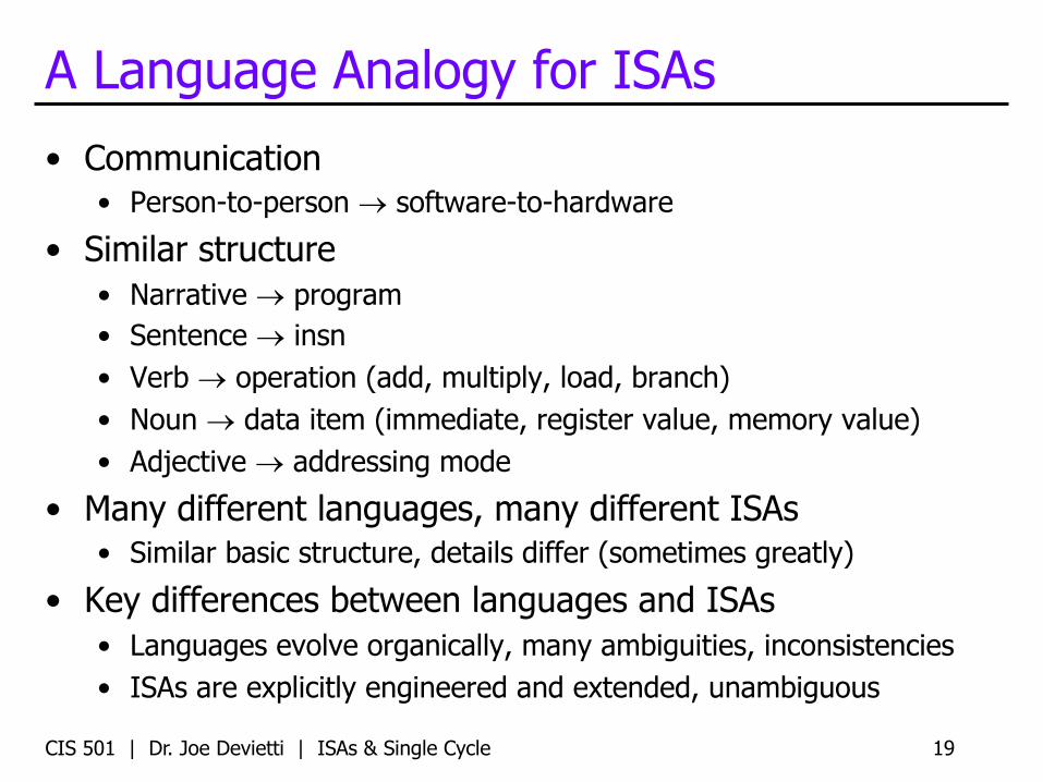
A Language Analogy for ISAs• Communication
• Person-to-person ® software-to-hardware• Similar structure
• Narrative ® program• Sentence ® insn• Verb ® operation (add, multiply, load, branch)• Noun ® data item (immediate, register value, memory value)• Adjective ® addressing mode
• Many different languages, many different ISAs• Similar basic structure, details differ (sometimes greatly)
• Key differences between languages and ISAs• Languages evolve organically, many ambiguities, inconsistencies• ISAs are explicitly engineered and extended, unambiguous
CIS 501 | Dr. Joe Devietti | ISAs & Single Cycle 20
LC4 vs Real ISAs
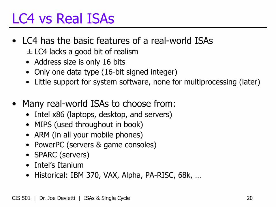
• LC4 has the basic features of a real-world ISAs
±LC4 lacks a good bit of realism
• Address size is only 16 bits
• Only one data type (16-bit signed integer)
• Little support for system software, none for multiprocessing (later)
• Many real-world ISAs to choose from:
• Intel x86 (laptops, desktop, and servers)
• MIPS (used throughout in book)
• ARM (in all your mobile phones)
• PowerPC (servers & game consoles)
• SPARC (servers)
• Intel’s Itanium
• Historical: IBM 370, VAX, Alpha, PA-RISC, 68k, …
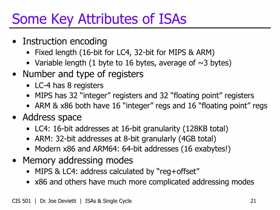
Some Key Attributes of ISAs• Instruction encoding
• Fixed length (16-bit for LC4, 32-bit for MIPS & ARM)• Variable length (1 byte to 16 bytes, average of ~3 bytes)
• Number and type of registers• LC-4 has 8 registers• MIPS has 32 “integer” registers and 32 “floating point” registers• ARM & x86 both have 16 “integer” regs and 16 “floating point” regs
• Address space• LC4: 16-bit addresses at 16-bit granularity (128KB total)• ARM: 32-bit addresses at 8-bit granularly (4GB total)• Modern x86 and ARM64: 64-bit addresses (16 exabytes!)
• Memory addressing modes• MIPS & LC4: address calculated by “reg+offset”• x86 and others have much more complicated addressing modes
CIS 501 | Dr. Joe Devietti | ISAs & Single Cycle 21
22
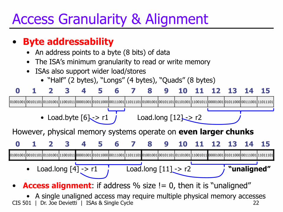
Access Granularity & Alignment• Byte addressability
• An address points to a byte (8 bits) of data• The ISA’s minimum granularity to read or write memory• ISAs also support wider load/stores
• “Half” (2 bytes), “Longs” (4 bytes), “Quads” (8 bytes)
• Load.byte [6] -> r1 Load.long [12] -> r2
However, physical memory systems operate on even larger chunks
• Load.long [4] -> r1 Load.long [11] -> r2 “unaligned”
• Access alignment: if address % size != 0, then it is “unaligned” • A single unaligned access may require multiple physical memory accesses
0 1 2 3 4 5 6 7 8 9 10 11 12 13 14 1501001001 00101101 01101001 11001011 00001001 01011000 00111001 11011101 01001001 00101101 01101001 11001011 00001001 01011000 00111001 11011101
0 1 2 3 4 5 6 7 8 9 10 11 12 13 14 1501001001 00101101 01101001 11001011 00001001 01011000 00111001 11011101 01001001 00101101 01101001 11001011 00001001 01011000 00111001 11011101
CIS 501 | Dr. Joe Devietti | ISAs & Single Cycle

23
Handling Unaligned Accesses• Access alignment: if address % size != 0, then it is “unaligned”
• A single unaligned access may require multiple physical memory accesses
• How to handle such unaligned accesses?1. Disallow (unaligned operations are considered illegal)
• MIPS, ARMv5 and earlier took this route2. Support in hardware? (allow such operations)
• x86, ARMv6+ allow regular loads/stores to be unaligned• Unaligned access still slower, adds significant hardware complexity
3. Trap to software routine?• Simpler hardware, but high penalty when unaligned
4. In software (compiler can use regular instructions when possibly unaligned• Load, shift, load, shift, and (slow, needs help from compiler)
CIS 501 | Dr. Joe Devietti | ISAs & Single Cycle
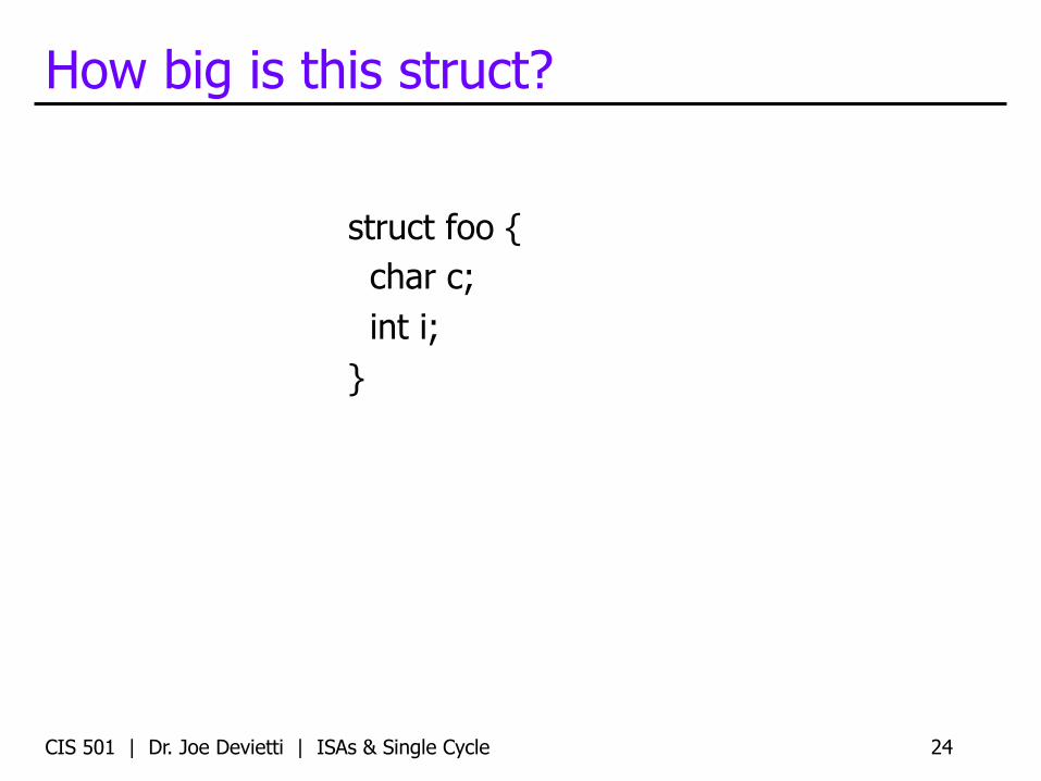
How big is this struct?
struct foo {char c;int i;
}
24CIS 501 | Dr. Joe Devietti | ISAs & Single Cycle

25
Another Addressing Issue: Endian-ness• Endian-ness: arrangement of bytes in a multi-byte number
• Big-endian: sensible order (e.g., MIPS, PowerPC, ARM) • A 4-byte integer: “00000000 00000000 00000010 00000011” is 515
• Little-endian: reverse order (e.g., x86)• A 4-byte integer: “00000011 00000010 00000000 00000000” is 515
• Why little endian?
00000011 00000010 00000000 00000000
starting addressinteger casts are free on little-endian architectures
CIS 501 | Dr. Joe Devietti | ISAs & Single Cycle
ISA Code Examples
CIS 501 | Dr. Joe Devietti | ISAs & Single Cycle 26

Array Sum Loop: LC4
CIS 501 | Dr. Joe Devietti | ISAs & Single Cycle 27
.DATAarray .BLKW #100sum .FILL #0
.CODE
.FALIGNarray_sum
CONST R5, #0LEA R1, arrayLEA R2, sum
L1LDR R3, R1, #0LDR R4, R2, #0ADD R4, R3, R4STR R4, R2, #0ADD R1, R1, #1ADD R5, R5, #1CMPI R5, #100BRn L1
int array[100];int sum;void array_sum() {
for (int i=0; i<100;i++) {
sum += array[i];}
}

Array Sum Loop: LC4 è MIPS
CIS 501 | Dr. Joe Devietti | ISAs & Single Cycle 28
.DATAarray .BLKW #100sum .FILL #0
.CODE
.FALIGNarray_sum
CONST R5, #0LEA R1, arrayLEA R2, sum
L1LDR R3, R1, #0LDR R4, R2, #0ADD R4, R3, R4STR R4, R2, #0ADD R1, R1, #1ADD R5, R5, #1CMPI R5, #100BRn L1
.dataarray: .space 100sum: .word 0
.textarray_sum:
li $5, 0la $1, arrayla $2, sum
L1:lw $3, 0($1)lw $4, 0($2)add $4, $3, $4sw $4, 0($2)addi $1, $1, 1addi $5, $5, 1li $6, 100blt $5, $6, L1
Syntactic differences:register names begin with $immediates are un-prefixed
MIPS (right) similar to LC4
Only simple addressing modessyntax: displacement(reg)
Left-most register is generally destination register

Array Sum Loop: LC4 è x86
CIS 501 | Dr. Joe Devietti | ISAs & Single Cycle 29
.DATAarray .BLKW #100sum .FILL #0
.CODE
.FALIGNarray_sum
CONST R5, #0LEA R1, arrayLEA R2, sum
L1LDR R3, R1, #0LDR R4, R2, #0ADD R4, R3, R4STR R4, R2, #0ADD R1, R1, #1ADD R5, R5, #1CMPI R5, #100BRn L1
.LFE2
.comm array,400,32
.comm sum,4,4
.globl array_sumarray_sum:
movl $0, -4(%rbp)
.L1:movl -4(%rbp), %eaxmovl array(,%eax,4), %edxmovl sum(%rip), %eax addl %edx, %eaxmovl %eax, sum(%rip)addl $1, -4(%rbp)cmpl $99,-4(%rbp)jle .L1
x86 (right) is different
Syntactic differences:register names begin with %immediates begin with $
%rbp is base (frame) pointer
Many addressing modes

x86 Operand Model
• x86 uses explicit accumulators• Both register and memory
• Distinguished by addressing mode
CIS 501 | Dr. Joe Devietti | ISAs & Single Cycle 30
.LFE2.comm array,400,32.comm sum,4,4
.globl array_sumarray_sum:
movl $0, -4(%rbp)
.L1:movl -4(%rbp), %eaxmovl array(,%eax,4), %edxmovl sum(%rip), %eaxaddl %edx, %eaxmovl %eax, sum(%rip)addl $1, -4(%rbp)cmpl $99,-4(%rbp)jle .L1
Register accumulator: %eax = %eax + %edx
Memory accumulator: Memory[%rbp-4] = Memory[%rbp-4] + 1
Two operand insns(right-most is typically source & destination)
“L” insn suffix and “%e…” reg. prefix mean “32-bit value”

CIS 501 | Dr. Joe Devietti | ISAs & Single Cycle 31

Implementing an ISA
CIS 501 | Dr. Joe Devietti | ISAs & Single Cycle 32
CIS 501 | Dr. Joe Devietti | ISAs & Single Cycle 33
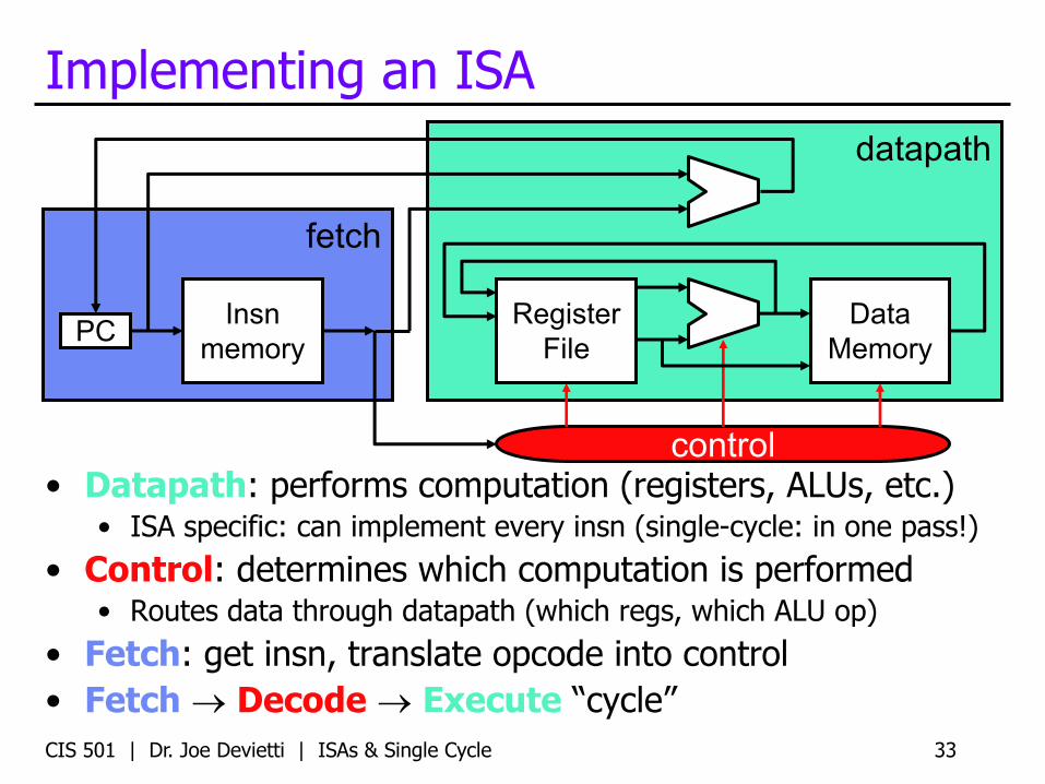
Implementing an ISA
• Datapath: performs computation (registers, ALUs, etc.)• ISA specific: can implement every insn (single-cycle: in one pass!)
• Control: determines which computation is performed • Routes data through datapath (which regs, which ALU op)
• Fetch: get insn, translate opcode into control• Fetch ® Decode ® Execute “cycle”
PC Insnmemory
RegisterFile
DataMemory
control
datapath
fetch

CIS 501 | Dr. Joe Devietti | ISAs & Single Cycle 34
Two Types of Components
• Purely combinational: stateless computation• ALUs, muxes, control• Arbitrary Boolean functions
• Combinational/sequential: storage• PC, insn/data memories, register file• Internally contain some combinational components
PC Insnmemory
RegisterFile
DataMemory
control
datapath
fetch

Example Datapath
CIS 501 | Dr. Joe Devietti | ISAs & Single Cycle 35

PCMemory216 by 16 bit
1616
16
3’b111
insn[11:9] 3
BranchLogic
16
16
LC4 Datapath
Reg.File
wdata
3’b111
insn[11:9] 3
insn[11:9]
insn[2:0] 3
Reg.File
r1sel r2selr1data
r2data
wselwe
NZP Regwe
NZP Reg3
16
16
16
Memory216 by 16 bit
in
outaddr we
16
n/z/p3
insn[8:6]
16
ALU
+1
36CIS 501 | Dr. Joe Devietti | ISAs & Single Cycle

MIPS Datapath
CIS 501 | Dr. Joe Devietti | ISAs & Single Cycle 37

CIS 501 | Dr. Joe Devietti | ISAs & Single Cycle 38
Unified vs Split Memory Architecture
• Unified architecture: unified insn/data memory• “Harvard” architecture: split insn/data memories
PC RegisterFile
Insn/Data Memory
control
datapath
fetch

CIS 501 | Dr. Joe Devietti | ISAs & Single Cycle 39
Datapath for MIPS ISA
• MIPS: 32-bit instructions, registers are $0, $2… $31
• Consider only the following instructions
add $1,$2,$3 $1 = $2 + $3 (add)addi $1,$2,3 $1 = $2 + 3 (add immed)lw $1,4($3) $1 = Memory[4+$3] (load)sw $1,4($3) Memory[4+$3] = $1 (store)beq $1,$2,PC_relative_target (branch equal)j absolute_target (unconditional jump)
• Why only these?
• Most other instructions are the same from datapath viewpoint
• The ones that aren’t are left for you to figure out J

MIPS Instruction layout
CIS 501 | Dr. Joe Devietti | ISAs & Single Cycle 40
2/6/14, 11:36 AMMorgan Kaufmann Series in Computer Architecture and Design : Computer…vised Fourth Edition : The Hardware/Software Interface (4th Edition)
Page 1 of 2http://site.ebrary.com/lib/upenn/docPrint.action?encrypted=e1!d7c…0a7916bf43cd7114bd5ddd1a046e03f1fe886!5104c57021174f54aa81b206f44
Patterson, David A.; Hennessy, John L.. Morgan Kaufmann Series in Computer Architecture and Design : Computer Organization and Design, RevisedFourth Edition : The Hardware/Software Interface (4th Edition).St. Louis, MO, USA: Morgan Kaufmann, 2011. p 125.http://site.ebrary.com/lib/upenn/Doc?id=10509203&ppg=125

CIS 501 | Dr. Joe Devietti | ISAs & Single Cycle 41
Start With Fetch
• PC and instruction memory (split insn/data architecture, for now)• A +4 incrementer computes default next instruction PC• How would Verilog for this look given insn memory as interface?
PC
InsnMem
+4

CIS 501 | Dr. Joe Devietti | ISAs & Single Cycle 42
First Instruction: add
• Add register file• Add arithmetic/logical unit (ALU)
PC
InsnMem
RegisterFile
Op(6) Rs(5) Rt(5) Rd(5) Sh(5) Func(6)R-type
s1 s2 d
+4
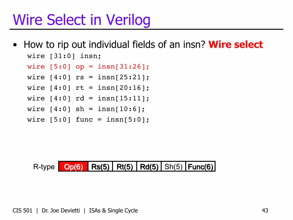
Wire Select in Verilog• How to rip out individual fields of an insn? Wire select
wire [31:0] insn;wire [5:0] op = insn[31:26];wire [4:0] rs = insn[25:21];wire [4:0] rt = insn[20:16];wire [4:0] rd = insn[15:11];wire [4:0] sh = insn[10:6];wire [5:0] func = insn[5:0];
CIS 501 | Dr. Joe Devietti | ISAs & Single Cycle 43
Op(6) Rs(5) Rt(5) Rd(5) Sh(5) Func(6)R-type

CIS 501 | Dr. Joe Devietti | ISAs & Single Cycle 44
Second Instruction: addi
• Destination register can now be either Rd or Rt• Add sign extension unit and mux into second ALU input
PC
InsnMem
RegisterFile
SX
Op(6) Rs(5) Rt(5)I-type Immed(16)
s1 s2 d
+4
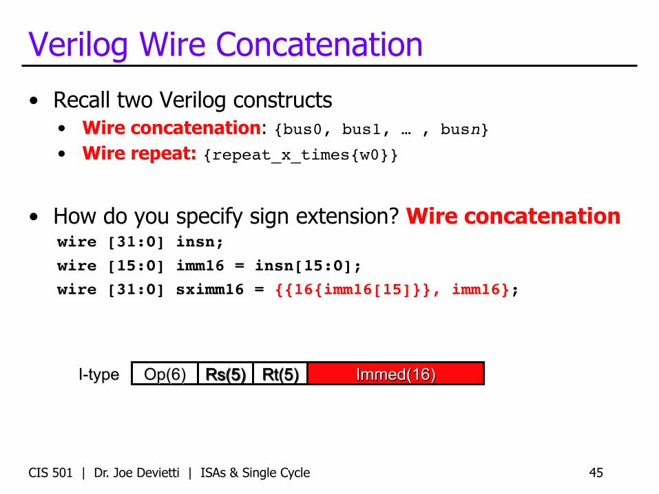
Verilog Wire Concatenation• Recall two Verilog constructs
• Wire concatenation: {bus0, bus1, … , busn}• Wire repeat: {repeat_x_times{w0}}
• How do you specify sign extension? Wire concatenationwire [31:0] insn;wire [15:0] imm16 = insn[15:0];wire [31:0] sximm16 = {{16{imm16[15]}}, imm16};
CIS 501 | Dr. Joe Devietti | ISAs & Single Cycle 45
Op(6) Rs(5) Rt(5)I-type Immed(16)

CIS 501 | Dr. Joe Devietti | ISAs & Single Cycle 46
Third Instruction: lw
• Add data memory, address is ALU output• Add register write data mux to select memory output or ALU output
PC
InsnMem
RegisterFile
SX
Op(6) Rs(5) Rt(5)I-type Immed(16)
s1 s2 d
DataMem
a
d
+4
CIS 501 | Dr. Joe Devietti | ISAs & Single Cycle 47
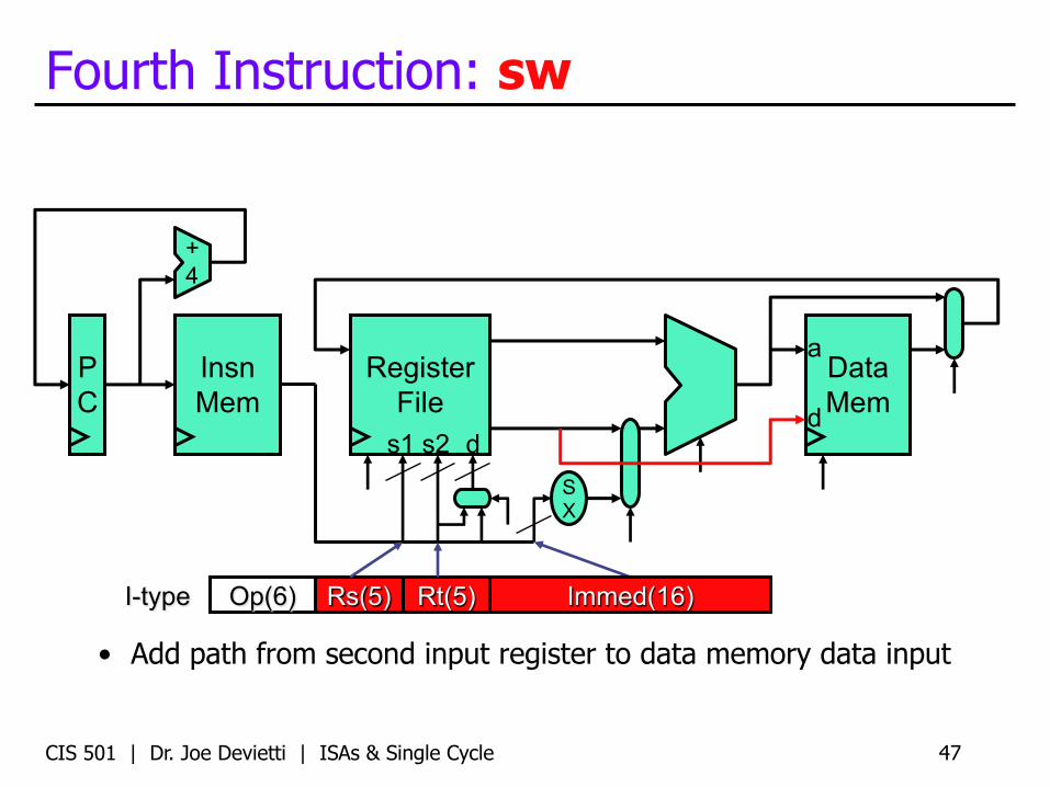
Fourth Instruction: sw
• Add path from second input register to data memory data input
PC
InsnMem
RegisterFile
SX
Op(6) Rs(5) Rt(5)I-type Immed(16)
s1 s2 d
DataMem
a
d
+4

CIS 501 | Dr. Joe Devietti | ISAs & Single Cycle 48
Fifth Instruction: beq
• Add left shift unit and adder to compute PC-relative branch target• Add PC input mux to select PC+4 or branch target
PC
InsnMem
RegisterFile
SX
Op(6) Rs(5) Rt(5)I-type Immed(16)
s1 s2 d
DataMem
a
d
+4
<<2
z

Another Use of Wire Concatenation• How do you do <<2? Wire concatenation
wire [31:0] insn;wire [25:0] imm26 = insn[25:0]wire [31:0] imm26_shifted_by_2 = {4’b0000, imm26, 2’b00};
CIS 501 | Dr. Joe Devietti | ISAs & Single Cycle 49
Op(6) Immed(26)
CIS 501 | Dr. Joe Devietti | ISAs & Single Cycle 50
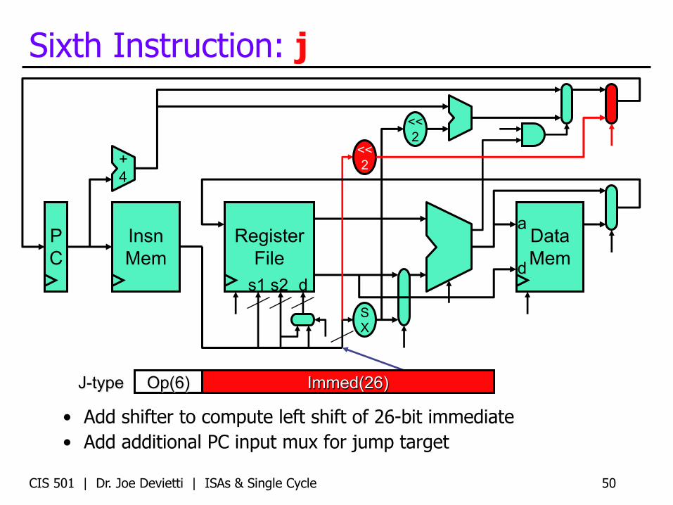
Sixth Instruction: j
• Add shifter to compute left shift of 26-bit immediate• Add additional PC input mux for jump target
PC
InsnMem
RegisterFile
SX
Op(6)J-type Immed(26)
s1 s2 d
DataMem
a
d
+4
<<2
<<2

MIPS Control
CIS 501 | Dr. Joe Devietti | ISAs & Single Cycle 51
CIS 501 | Dr. Joe Devietti | ISAs & Single Cycle 52
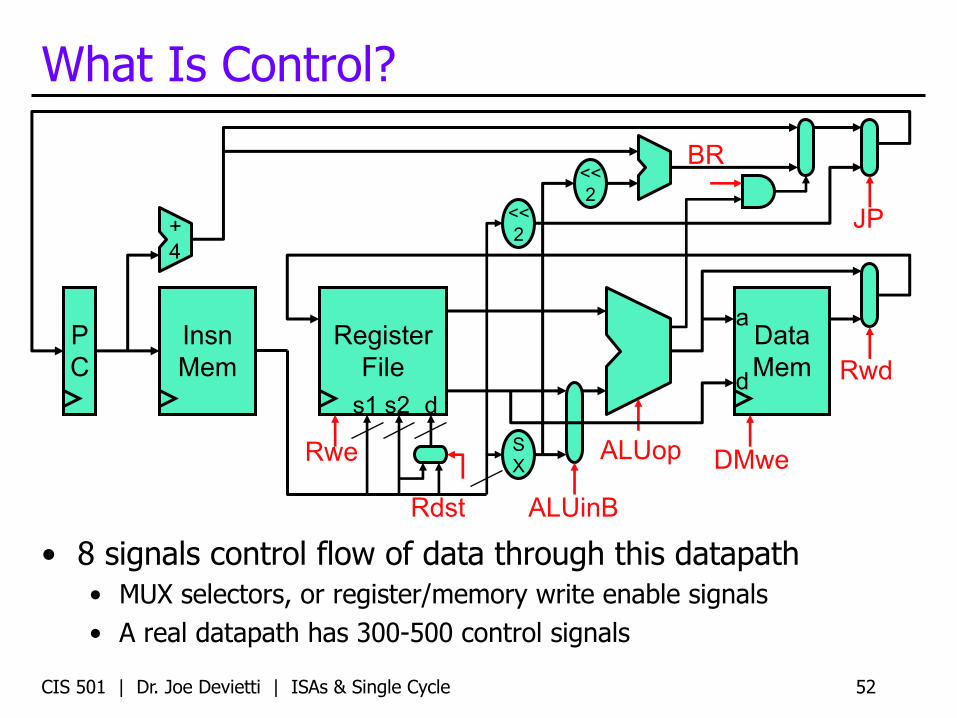
What Is Control?
• 8 signals control flow of data through this datapath• MUX selectors, or register/memory write enable signals• A real datapath has 300-500 control signals
PC
InsnMem
RegisterFile
SX
s1 s2 d
DataMem
a
d
+4
<<2
<<2
Rwe
ALUinB
DMwe
JP
ALUop
BR
Rwd
Rdst

CIS 501 | Dr. Joe Devietti | ISAs & Single Cycle 53
Example: Control for add
PC
InsnMem
RegisterFile
SX
s1 s2 d
DataMem
a
d
+4
<<2
<<2
BR=0
JP=0
Rwd=0
DMwe=0ALUop=0
ALUinB=0Rdst=1
Rwe=1

CIS 501 | Dr. Joe Devietti | ISAs & Single Cycle 54
Example: Control for sw
• Difference between sw and add is 5 signals• 3 if you don’t count the X (don’t care) signals
PC
InsnMem
RegisterFile
SX
s1 s2 d
DataMem
a
d
+4
<<2
<<2
Rwe=0
ALUinB=1
DMwe=1
JP=0
ALUop=0
BR=0
Rwd=X
Rdst=X

CIS 501 | Dr. Joe Devietti | ISAs & Single Cycle 55
Example: Control for beq
• Difference between sw and beq is only 4 signals
PC
InsnMem
RegisterFile
SX
s1 s2 d
DataMem
a
d
+4
<<2
<<2
Rwe=0
ALUinB=0
DMwe=0
JP=0
ALUop=1
BR=1
Rwd=X
Rdst=X

CIS 501 | Dr. Joe Devietti | ISAs & Single Cycle 56
How Is Control Implemented?
PC
InsnMem
RegisterFile
SX
s1 s2 d
DataMem
a
d
+4
<<2
<<2
Rwe
ALUinB
DMwe
JP
ALUop
BR
Rwd
Rdst
Control?
CIS 501 | Dr. Joe Devietti | ISAs & Single Cycle 57
Implementing Control• Each instruction has a unique set of control signals
• Most are function of opcode• Some may be encoded in the instruction itself
• E.g., the ALUop signal is some portion of the MIPS Func field+ Simplifies controller implementation• Requires careful ISA design
CIS 501 | Dr. Joe Devietti | ISAs & Single Cycle 58
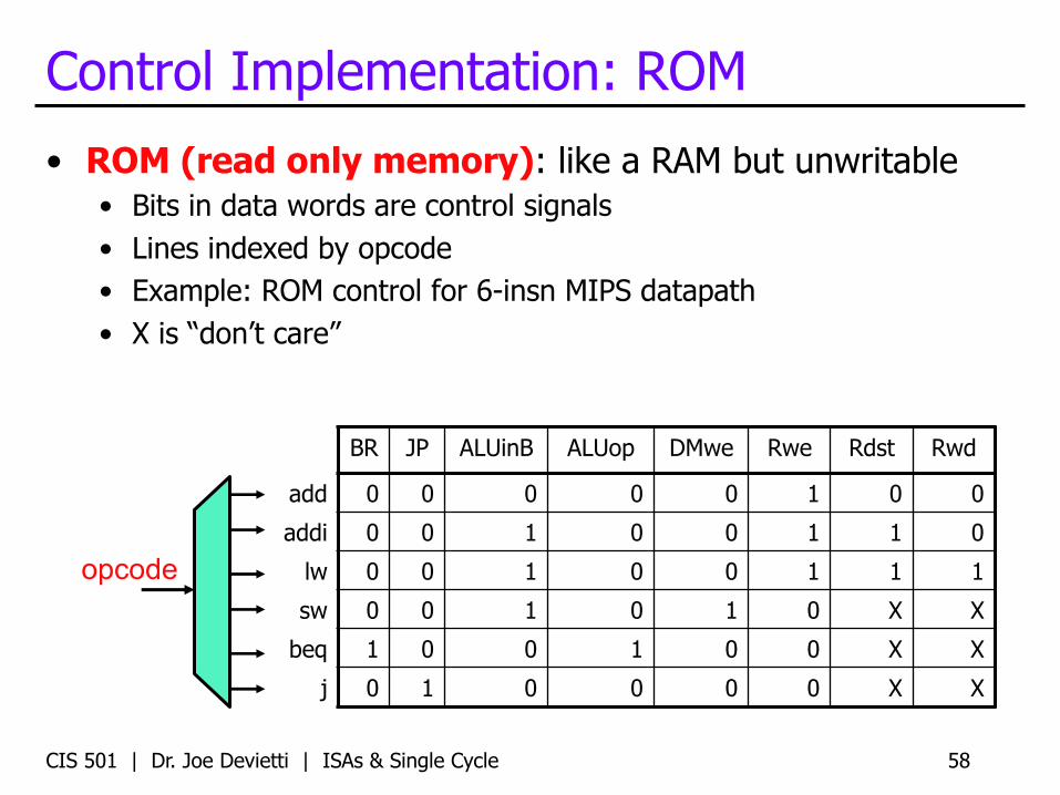
Control Implementation: ROM• ROM (read only memory): like a RAM but unwritable
• Bits in data words are control signals• Lines indexed by opcode• Example: ROM control for 6-insn MIPS datapath• X is “don’t care”
BR JP ALUinB ALUop DMwe Rwe Rdst Rwd
add 0 0 0 0 0 1 0 0addi 0 0 1 0 0 1 1 0
lw 0 0 1 0 0 1 1 1sw 0 0 1 0 1 0 X X
beq 1 0 0 1 0 0 X Xj 0 1 0 0 0 0 X X
opcode
CIS 501 | Dr. Joe Devietti | ISAs & Single Cycle 59
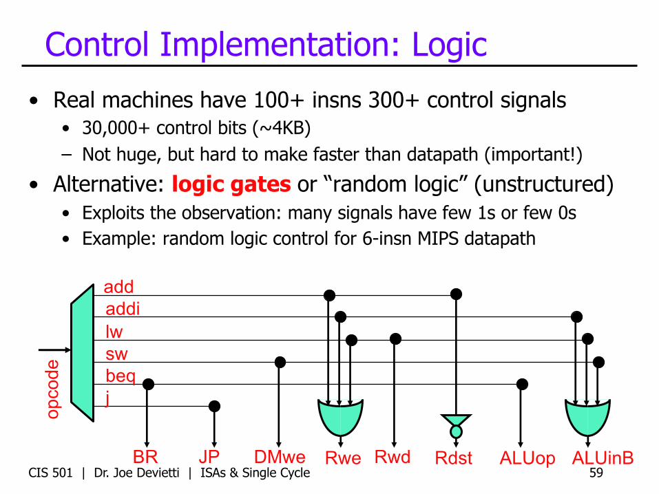
Control Implementation: Logic
• Real machines have 100+ insns 300+ control signals• 30,000+ control bits (~4KB)
– Not huge, but hard to make faster than datapath (important!)
• Alternative: logic gates or “random logic” (unstructured)
• Exploits the observation: many signals have few 1s or few 0s
• Example: random logic control for 6-insn MIPS datapath
ALUinB
opcode
addaddilwswbeqj
BR JP DMwe Rwd Rdst ALUopRwe
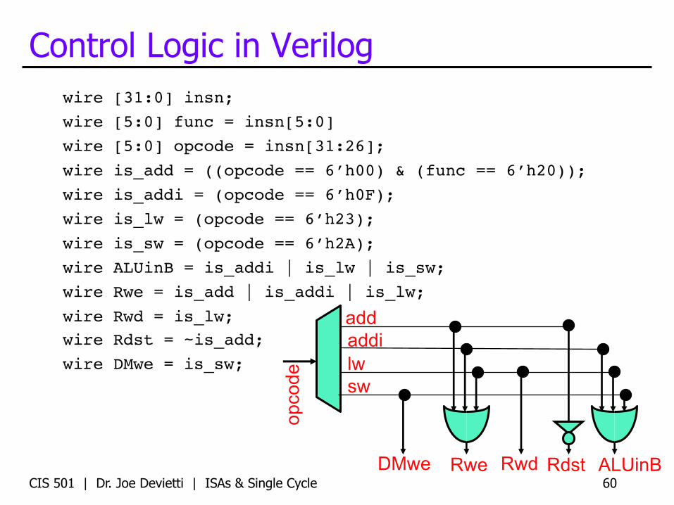
Control Logic in Verilogwire [31:0] insn;wire [5:0] func = insn[5:0]wire [5:0] opcode = insn[31:26];wire is_add = ((opcode == 6’h00) & (func == 6’h20));wire is_addi = (opcode == 6’h0F);wire is_lw = (opcode == 6’h23);wire is_sw = (opcode == 6’h2A);wire ALUinB = is_addi | is_lw | is_sw; wire Rwe = is_add | is_addi | is_lw;wire Rwd = is_lw;wire Rdst = ~is_add;wire DMwe = is_sw;
CIS 501 | Dr. Joe Devietti | ISAs & Single Cycle 60ALUinB
opcode
addaddilwsw
DMwe Rwd RdstRwe

Datapath Storage Elements
CIS 501 | Dr. Joe Devietti | ISAs & Single Cycle 61
CIS 501 | Dr. Joe Devietti | ISAs & Single Cycle 62
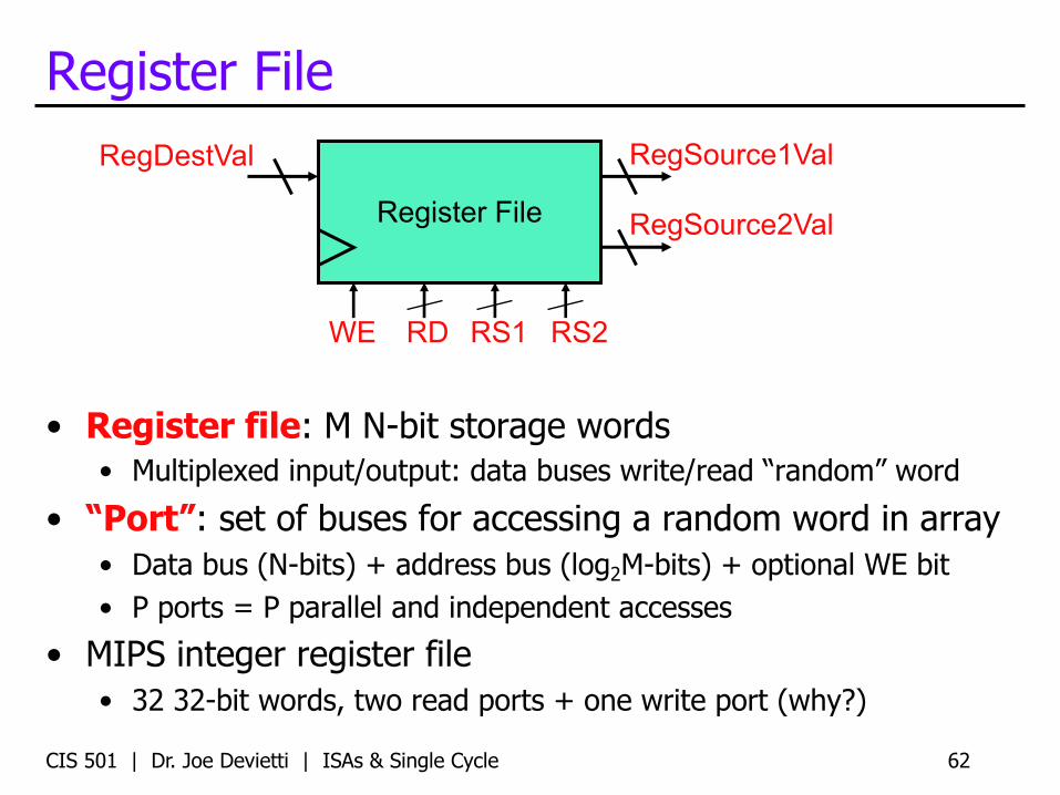
Register File
• Register file: M N-bit storage words• Multiplexed input/output: data buses write/read “random” word
• “Port”: set of buses for accessing a random word in array• Data bus (N-bits) + address bus (log2M-bits) + optional WE bit• P ports = P parallel and independent accesses
• MIPS integer register file• 32 32-bit words, two read ports + one write port (why?)
Register File
RegSource1Val
RegSource2Val
RegDestVal
RDWE RS1 RS2

CIS 501 | Dr. Joe Devietti | ISAs & Single Cycle 63
Decoder
• Decoder: converts binary integer to “1-hot” representation
• Binary representation of 0…2N–1: N bits
• 1 hot representation of 0…2N–1: 2N bits
• J represented as Jth bit 1, all other bits zero
• Example below: 2-to-4 decoder
B[0]
B[1]1H[0]
1H[1]
1H[2]
1H[3]
B 1H
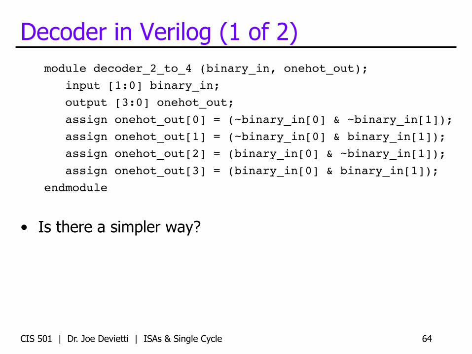
Decoder in Verilog (1 of 2)module decoder_2_to_4 (binary_in, onehot_out);
input [1:0] binary_in; output [3:0] onehot_out;assign onehot_out[0] = (~binary_in[0] & ~binary_in[1]);assign onehot_out[1] = (~binary_in[0] & binary_in[1]);assign onehot_out[2] = (binary_in[0] & ~binary_in[1]);assign onehot_out[3] = (binary_in[0] & binary_in[1]);
endmodule
• Is there a simpler way?
CIS 501 | Dr. Joe Devietti | ISAs & Single Cycle 64

Decoder in Verilog (2 of 2)module decoder_2_to_4 (binary_in, onehot_out);
input [1:0] binary_in; output [3:0] onehot_out;assign onehot_out[0] = (binary_in == 2’d0);assign onehot_out[1] = (binary_in == 2’d1);assign onehot_out[2] = (binary_in == 2’d2);assign onehot_out[3] = (binary_in == 2’d3);
endmodule
• How is “a == b“ implemented for vectors?• ~|(a ^ b) (this is a “nor” reduction of bitwise “a xor b”)• When one of the inputs to “==“ is a constant
• Simplifies to simpler inverter on bits with “one” in constant• Exactly what was on previous slide! (apply DeMorgan’s law)
CIS 501 | Dr. Joe Devietti | ISAs & Single Cycle 65
CIS 501 | Dr. Joe Devietti | ISAs & Single Cycle 66
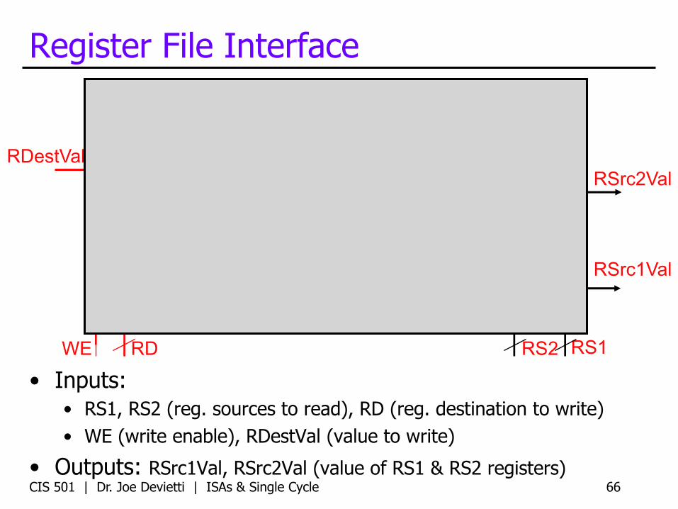
Register File Interface
• Inputs:• RS1, RS2 (reg. sources to read), RD (reg. destination to write)• WE (write enable), RDestVal (value to write)
• Outputs: RSrc1Val, RSrc2Val (value of RS1 & RS2 registers)
RS1
RSrc1Val
RSrc2Val
RS2RDWE
RDestVal
CIS 501 | Dr. Joe Devietti | ISAs & Single Cycle 67
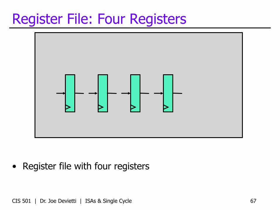
Register File: Four Registers
• Register file with four registers

CIS 501 | Dr. Joe Devietti | ISAs & Single Cycle 68
Add a Read Port
• Output of each register into 4to1 mux (RSrc1Val)• RS1 is select input of RSrc1Val mux
RS1
RSrc1Val

CIS 501 | Dr. Joe Devietti | ISAs & Single Cycle 69
Add Another Read Port
• Output of each register into another 4to1 mux (RSrc2Val)• RS2 is select input of RSrc2Val mux
RS1
RSrc1Val
RSrc2Val
RS2

CIS 501 | Dr. Joe Devietti | ISAs & Single Cycle 70
Add a Write Port
• Input RegDestVal into each register• Enable only one register’s WE: (Decoded RD) & (WE)
• What if we needed two write ports?
RS1
RSrc1Val
RSrc2Val
RS2RDWE
RDestVal

Register File Interface (Verilog)module regfile4(rs1, rs1val, rs2, rs2val, rd, rdval, we, rst, clk);
parameter n = 1; input [1:0] rs1, rs2, rd; input we, rst, clk;input [n-1:0] rdval; output [n-1:0] rs1val, rs2val;…
endmodule
• Building block modules:• module register (out, in, wen, rst, clk);• module decoder_2_to_4 (binary_in, onehot_out)• module Nbit_mux4to1 (sel, a, b, c, d, out);
CIS 501 | Dr. Joe Devietti | ISAs & Single Cycle 71
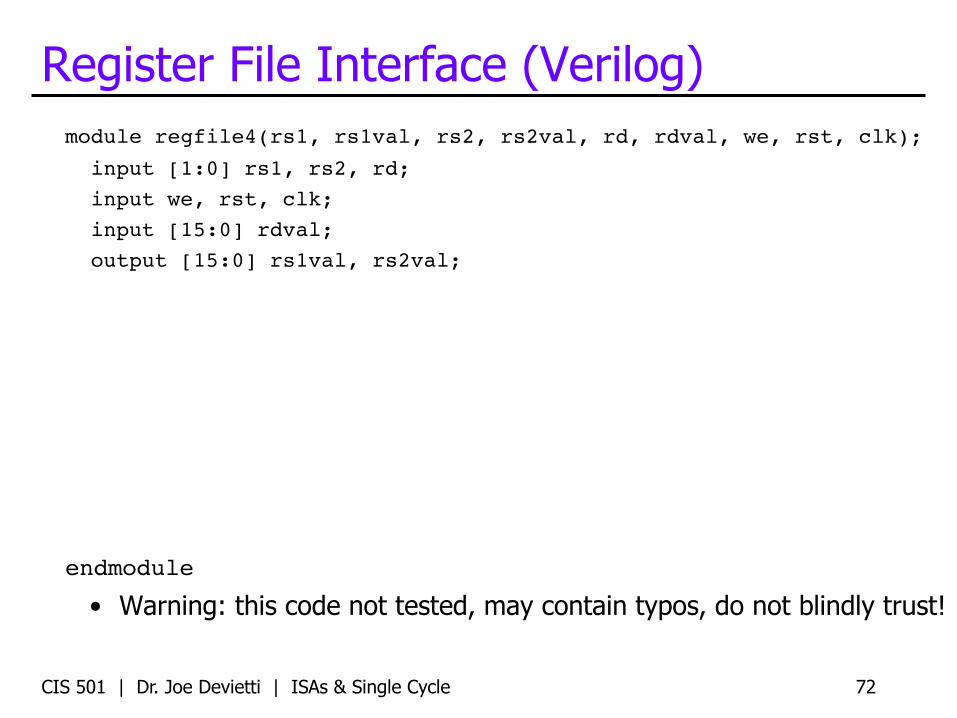
Register File Interface (Verilog)module regfile4(rs1, rs1val, rs2, rs2val, rd, rdval, we, rst, clk);
input [1:0] rs1, rs2, rd; input we, rst, clk;input [15:0] rdval; output [15:0] rs1val, rs2val;
endmodule• Warning: this code not tested, may contain typos, do not blindly trust!
CIS 501 | Dr. Joe Devietti | ISAs & Single Cycle 72
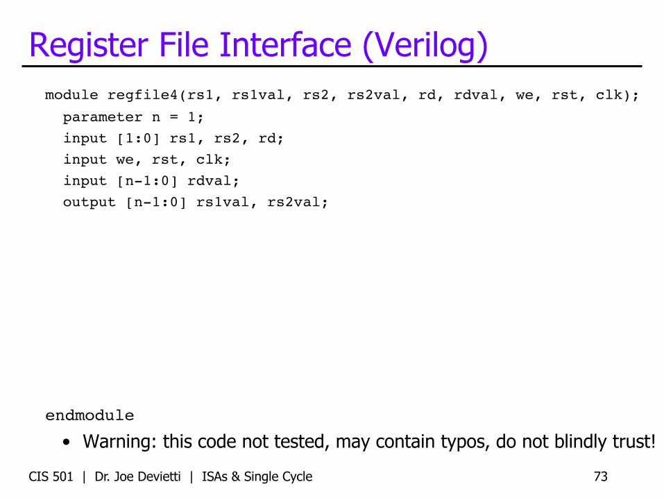
Register File Interface (Verilog)module regfile4(rs1, rs1val, rs2, rs2val, rd, rdval, we, rst, clk);
parameter n = 1; input [1:0] rs1, rs2, rd; input we, rst, clk;input [n-1:0] rdval; output [n-1:0] rs1val, rs2val;
endmodule• Warning: this code not tested, may contain typos, do not blindly trust!
CIS 501 | Dr. Joe Devietti | ISAs & Single Cycle 73

Register File: Four Registers (Verilog)module regfile4(rs1, rs1val, rs2, rs2val, rd, rdval, we, rst, clk);
parameter n = 1; input [1:0] rs1, rs2, rd; input we, rst, clk;input [n-1:0] rdval; output [n-1:0] rs1val, rs2val;wire [n-1:0] r0v, r1v, r2v, r3v;
Nbit_reg #(n) r0 (r0v, , , rst, clk);Nbit_reg #(n) r1 (r1v, , , rst, clk);Nbit_reg #(n) r2 (r2v, , , rst, clk);Nbit_reg #(n) r3 (r3v, , , rst, clk);
endmodule• Warning: this code not tested, may contain typos, do not blindly trust!
CIS 501 | Dr. Joe Devietti | ISAs & Single Cycle 74
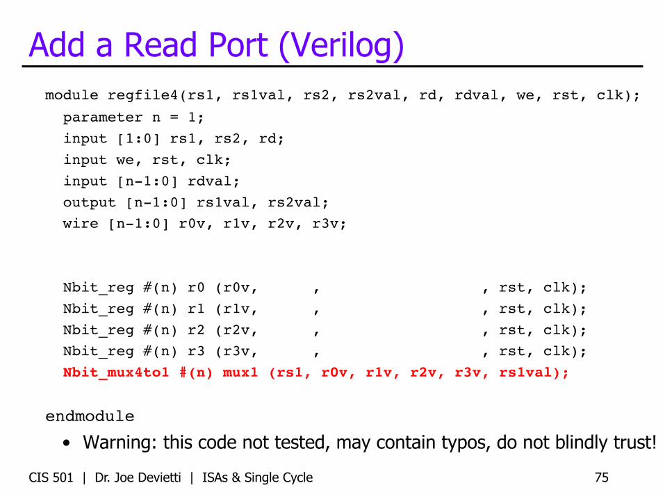
Add a Read Port (Verilog)module regfile4(rs1, rs1val, rs2, rs2val, rd, rdval, we, rst, clk);
parameter n = 1; input [1:0] rs1, rs2, rd; input we, rst, clk;input [n-1:0] rdval; output [n-1:0] rs1val, rs2val;wire [n-1:0] r0v, r1v, r2v, r3v;
Nbit_reg #(n) r0 (r0v, , , rst, clk);Nbit_reg #(n) r1 (r1v, , , rst, clk);Nbit_reg #(n) r2 (r2v, , , rst, clk);Nbit_reg #(n) r3 (r3v, , , rst, clk);Nbit_mux4to1 #(n) mux1 (rs1, r0v, r1v, r2v, r3v, rs1val);
endmodule• Warning: this code not tested, may contain typos, do not blindly trust!
CIS 501 | Dr. Joe Devietti | ISAs & Single Cycle 75

Add Another Read Port (Verilog)module regfile4(rs1, rs1val, rs2, rs2val, rd, rdval, we, rst, clk);
parameter n = 1; input [1:0] rs1, rs2, rd; input we, rst, clk;input [n-1:0] rdval; output [n-1:0] rs1val, rs2val;wire [n-1:0] r0v, r1v, r2v, r3v;
Nbit_reg #(n) r0 (r0v, , , rst, clk);Nbit_reg #(n) r1 (r1v, , , rst, clk);Nbit_reg #(n) r2 (r2v, , , rst, clk);Nbit_reg #(n) r3 (r3v, , , rst, clk);Nbit_mux4to1 #(n) mux1 (rs1, r0v, r1v, r2v, r3v, rs1val);Nbit_mux4to1 #(n) mux2 (rs2, r0v, r1v, r2v, r3v, rs2val);
endmodule• Warning: this code not tested, may contain typos, do not blindly trust!
CIS 501 | Dr. Joe Devietti | ISAs & Single Cycle 76

Add a Write Port (Verilog)module regfile4(rs1, rs1val, rs2, rs2val, rd, rdval, we, rst, clk);
parameter n = 1; input [1:0] rs1, rs2, rd; input we, rst, clk;input [n-1:0] rdval; output [n-1:0] rs1val, rs2val;wire [n-1:0] r0v, r1v, r2v, r3v;wire [3:0] rd_select; decoder_2_to_4 dec (rd, rd_select);Nbit_reg #(n) r0 (r0v, rdval, rd_select[0] & we, rst, clk);Nbit_reg #(n) r1 (r1v, rdval, rd_select[1] & we, rst, clk);Nbit_reg #(n) r2 (r2v, rdval, rd_select[2] & we, rst, clk);Nbit_reg #(n) r3 (r3v, rdval, rd_select[3] & we, rst, clk);Nbit_mux4to1 #(n) mux1 (rs1, r0v, r1v, r2v, r3v, rs1val);Nbit_mux4to1 #(n) mux2 (rs2, r0v, r1v, r2v, r3v, rs2val);
endmodule• Warning: this code not tested, may contain typos, do not blindly trust!
CIS 501 | Dr. Joe Devietti | ISAs & Single Cycle 77
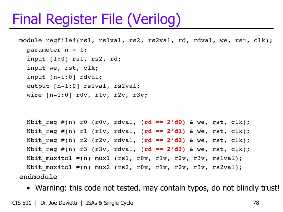
Final Register File (Verilog)module regfile4(rs1, rs1val, rs2, rs2val, rd, rdval, we, rst, clk);
parameter n = 1; input [1:0] rs1, rs2, rd; input we, rst, clk;input [n-1:0] rdval; output [n-1:0] rs1val, rs2val;wire [n-1:0] r0v, r1v, r2v, r3v;
Nbit_reg #(n) r0 (r0v, rdval, (rd == 2’d0) & we, rst, clk);Nbit_reg #(n) r1 (r1v, rdval, (rd == 2’d1) & we, rst, clk);Nbit_reg #(n) r2 (r2v, rdval, (rd == 2’d2) & we, rst, clk);Nbit_reg #(n) r3 (r3v, rdval, (rd == 2’d3) & we, rst, clk);Nbit_mux4to1 #(n) mux1 (rs1, r0v, r1v, r2v, r3v, rs1val);Nbit_mux4to1 #(n) mux2 (rs2, r0v, r1v, r2v, r3v, rs2val);
endmodule• Warning: this code not tested, may contain typos, do not blindly trust!
CIS 501 | Dr. Joe Devietti | ISAs & Single Cycle 78
CIS 501 | Dr. Joe Devietti | ISAs & Single Cycle 79
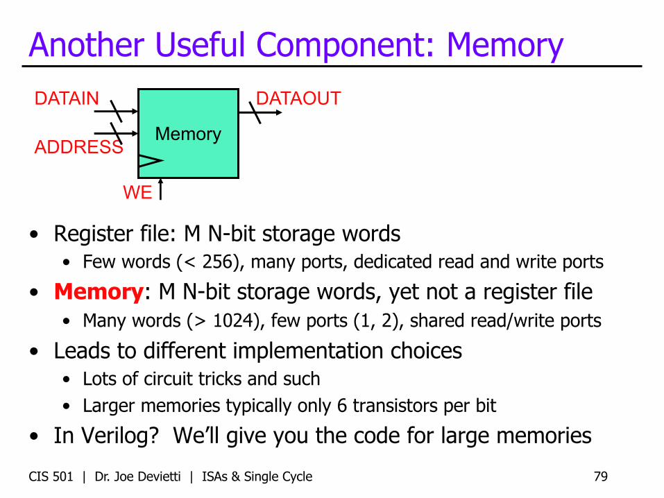
Another Useful Component: Memory
• Register file: M N-bit storage words• Few words (< 256), many ports, dedicated read and write ports
• Memory: M N-bit storage words, yet not a register file• Many words (> 1024), few ports (1, 2), shared read/write ports
• Leads to different implementation choices• Lots of circuit tricks and such• Larger memories typically only 6 transistors per bit
• In Verilog? We’ll give you the code for large memories
Memory
DATAOUTDATAIN
WE
ADDRESS

Single-Cycle Performance
CIS 501 | Dr. Joe Devietti | ISAs & Single Cycle 80
CIS 501 | Dr. Joe Devietti | ISAs & Single Cycle 81
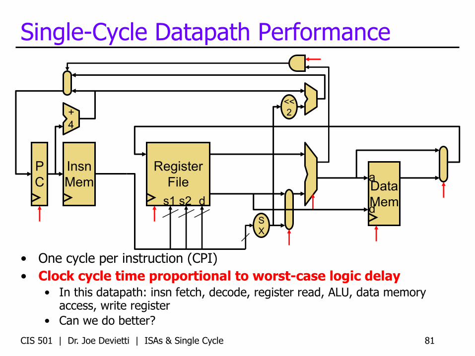
Single-Cycle Datapath Performance
• One cycle per instruction (CPI)• Clock cycle time proportional to worst-case logic delay
• In this datapath: insn fetch, decode, register read, ALU, data memory access, write register
• Can we do better?
PC
InsnMem
RegisterFile
SX
s1 s2 dDataMem
a
d
+4
<<2

CIS 501 | Dr. Joe Devietti | ISAs & Single Cycle 82
Foreshadowing: Pipelined Datapath
• Split datapath into multiple stages• Assembly line analogy• 5 stages results in up to 5x clock & performance improvement
PCInsnMem
RegisterFile
SX
s1 s2 dDataMem
a
d
+4
<<2
PC
IR
PC
A
B
IR
O
B
IR
O
D
IR

CIS 501 | Dr. Joe Devietti | ISAs & Single Cycle 83
Summary• Overview of ISAs• Datapath storage elements• MIPS Datapath• MIPS Control
CPUMem I/O
System softwareAppApp App