circuito similar admiral adv442ak
TRANSCRIPT
SERVICE MANUAL
TDE-F61PM\62PM\63PM\66P\68P\80P
1
Table of Contents
Failure & Troubleshooting of Power Supply .......................................................................................... 3
Troubleshooting and service of Decoder part .........................................................................................4-6
Figure 2. Basic Circuit Diagram ........................................................................................................... 2
Table of Contents .................................................................................................................... 1
Circuit diagram .................................................................................................................... ......Appendix
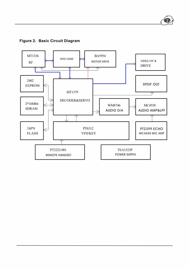
Figure 2 Basic Circuit Diagram
TEA1523P
AUDIOD/A AUDIOAMP&LPF
PT2399ECHO
EEPROM
MT1379
VFD/KEY
SDRAM
MT1336
2*16Mbit MC4558
POWERSUPPLY
PT2222-001
SPDIFOUT
RF
DECODER&SERVO
MC4558MICAMPFLASH
2402
BA5954
VIDEOLPF&DRIVE
MOTORDRIVED LOVADD
WM8746
REMOTEHANDSET
PT63121M*8
DVD LOADMOTOR DRIVE VIDEO LPF &
SPDIF OUT
AUDIO AMP&LPF
PT2399 ECHO
MC4558 MIC AMP
POWER SUPPLYREMOTE HANDSET
AUDIO D/A
2
1.1Principle of Power Supply Operation
This appliance adopts a switched-mode power supply, which is assembled with the TEA1523P
power switch module from Philips and is capable of protecting itself from over-current, over-voltage,
over-heat and short-circuit. The circuit mainly stabilizes a t +3.3v and fluctuate within a permissible
range, such as +5V, +12V, -12V, +3.3V and -24V. Please pay attention to the high voltage inside
the white silkscreen with the mark CAUTION on the PCB while repairing. When using an
oscillograph to check the circuit,an isolated transformer must be connected.
1.2Troubleshooting and Service
l+3.3V voltage varies out of the permissible range
Please check whether the sampling resistor R324 and R325 is eroded, and check if the voltage
of the first pin of the regulating fiducial IC U303 (TL431) is 2.5V. If the deviation is over 0.15V,
then TL431 is defected or eroded and needs to be replaced. When repairing, do not loop +3.3V
sampling circuit, that is, do not open-circuit D313, L306, R324, R325, R322, U302 (PC123Y) and
U303; otherwise, the output voltage will be too high and will damage the subsequent circuits.
lAll the output voltages are 0V and the voltage of the anode of capacitor C305 is over 150VCheck
whether +5V, +3.3V, +12V, -12V and -24V are short. Check if pin 3 of U301 has 100KHz vibrating
signal, if not, then U301 is eroded.
l+12V and +5V voltage are not normal, while other voltages are normalCheck whether D309,
R315, L303 and ZD303 are open or short, whether C315, C316 and C317 are short or
leak electricity. Any problem of these components will result in abnormal +12V and +5V voltage.
Open-circuit or short-circuit of D312, L305, ZD305, R319 and Q304, and electricity-leakage and
short-circuit of C324, C325, C326, C335 and C328 will result in abnormal +5V voltage.
l-24V and AC1-AC2 voltage are not normal, while other voltages are normalCheck whether R311,
D307, D308, R313, R312 and R314 are open or short, whether C312, C313 and C314 are short
or leak electricity.
lAll output voltages are under permissible range (refer to 2.2 of Chapter one)Check whether ZD
302, C308 and R303 are defected or eroded. If +3.3V output is normal and other voltages are
under range, check if the appliance is in standby mode. In standby mode, it is rational that all
voltages except +3.3V are not normal. If in playing mode, +3.3V output is normal, 5V output is
0V or too low, please check whether +5V is short-circuit and whether R320, Q305, ZD305, D312,
R319, C324, C325, C326, C328 and C335 are defected or eroded.
1.Troubleshooting and service of the Power Supply Board
3
2. Troubleshooting and Service of the Loader
a. No running of loader
a). Check whether the 24P ribbon wire to loader is in good contact.
b). Check whether +5V voltage is normal.
c). Check whether laser voltage ( about 2V for VCD and 2.2V for DVD respectively ) exists at the C
pole of Q1 and Q2, and whether U2 and adjacent parts are damaged or weld falsely.
d). If the above parts are normal and no laser emits, replace the loader.
b. Read no disc
a). Check whether the ribbon wire from 24P to loader is in good contact.
b). Check whether the RFO signal of the 10th pin of CN6 is transmitted to the 96th pin of U1.
c). Check whether laser voltage (about 2V for VCD and 2.2V for DVD respectively) exists at the C
pole of Q1 and Q2, and whether the voltage is normal.
d) Check whether U1, U2 and adjacent parts are damaged or weld falsely.
e). If the above parts are normal, replace U1 or the loader.
c. Read DVD discs only or read other discs beyond DVD only
a). Check whether the ribbon wire from 24P to loader is in good contact.
b). Check whether laser voltage of 2V outputs at the C pole of Q2, and whether the 125th pin of U1
is at low level.
c). Check whether the pins from the 1st to the 38th of U1 and adjacent parts are weld falsely,
damaged or erode.
d). If the above parts are normal, replace U1 or the loader.
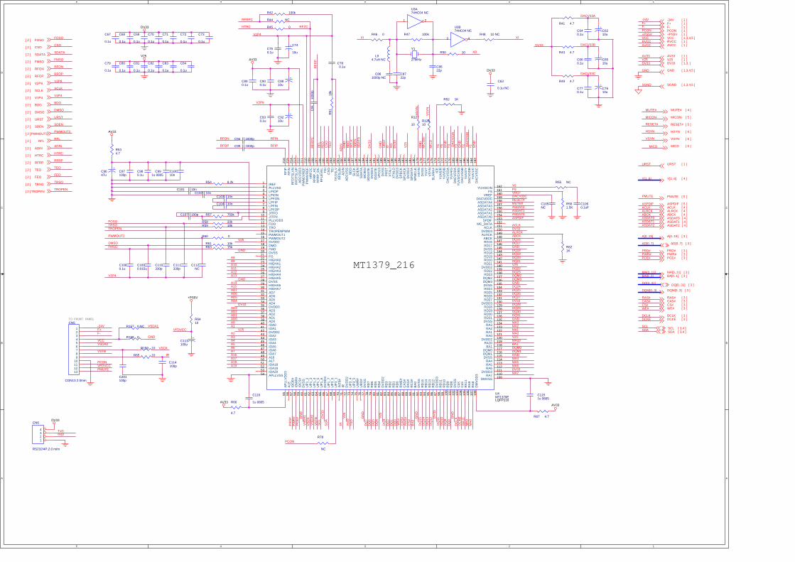
3. Troubleshooting and service of decoding part
a. No video, no audio, no display on VFD, and no operation of keys
a). Check whether the power sources of the decoder board are normal.
b). Check whether there is 27MHz signal output. If not, X1 crystal and adjacent parts are eroded or
damaged.
c). Check whether there is 81MHz signal output at R64. If not, check whether there is short circuit,
false welding or alien substance for audio D/A circuit U5 and SDRAM U8 and U9.
d). Check whether the reset circuit composed of C7, R37 and D1 is normal (constant 0V after tens
of milliseconds of high level). If it is at low level constantly, C7, R37 and D1 are damaged.
e). If the reset level is normal, check whether the chip selection signal, address and data of the 12th
pin of U5 are normal.
f). Check U10 that whether the data of pins from the 1st to the 8th, hsync and vsync signal of the
10th and 11th pins, and 27MHz signal of the 29th pin are normal, and whether C162 and R68 are
normal. If not, replace U10.
4
g). When U5 works normally, check the connection between U8, U9 and U3. If abnormal, replace U8
or U9.
h). Replace the main chip U3 after making sure no damage to the adjacent parts and no short circuit
or false welding for the circuit board.
4. Troubleshooting and service of video part1). Normal sound, no video picture
Check U10 that whether the data of pins from the 1st to the 8th, hsync and vsync signal of the 10th and 11th
pins, and 27MHz signal of the 29th pin are normal, and whether C162 and R68 are normal. If not, replace U10.
2). Abnormal color of the video picture
a). If there are horizontal or vertical streaks, or improper color appears on the picture after reading a disc, the
U3 decoding servo chip on the decoder board or U6 EEPROM may be in problems.
b). Check board whether the 3.3V and 2.5V power sources are normal, whether the ripple factor is too high,
and whether the data wire of Y(0, 7) between U3 and U10 is normal.
c). Check whether the video filter network circuit on the decoder board works normally.
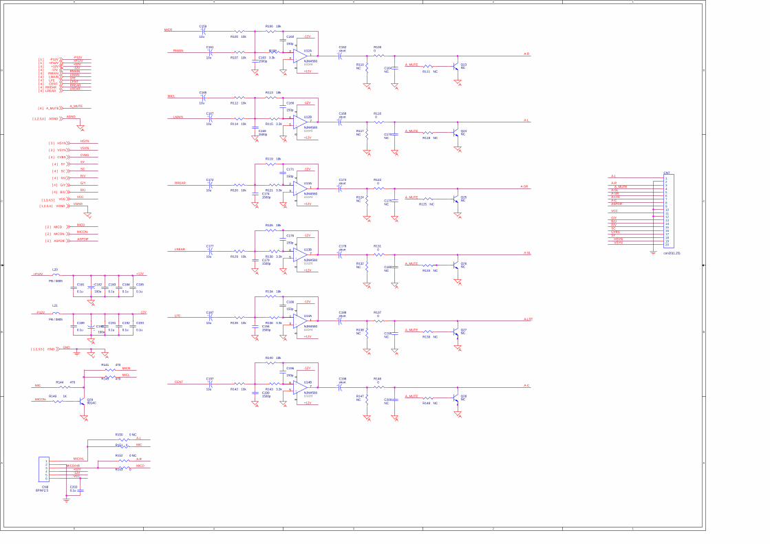
5. Troubleshooting and service of audio parta. Normal picture, no sound
a). Firstly, check whether the +8V and -8V power sources for the operational amplifier IC U12~U14 are normal.
b). Check whether the C poles of muting tube Q14, Q15, Q22, Q23, Q21 and Q20 are at low level constantly.
If so, the above tubes are not in good conditions.
c). Check whether the output of C poles of Q18 and Q19 are at high levels constantly. If so, Q18 and Q19 have
been broken down, or C209 are short.
d). Check whether the six audio signal lines on the 20P ribbon wire from decoder board to output board are in
good contact. If abnormal, replace the ribbon wire. Check the signal reaching the input of U12~U14. If the input
is normal while the output is not, replace the operational amplifier IC.
e). Check whether the signals of the 17th, 19th, 21st, 23rd, 25th and 27th pins of U5 on the decoder board are
normal. If not, check the signals of the pins from the 2nd to the 7th. If the clock signals of ACLK, ABCK and
ALRCK output by U3 are normal after R130, RN2 and R131 are disconnected, replace U11.
b. Distorted audio and loud noise
a). Firstly, check whether the +8V and -8V power sources for the operational amplifier IC U12~14 are normal.
b). Check whether the muting tubes are in good conditions.
c). Check whether the signals of the 17th, 19th, 21st, 23rd, 25th and 27th pins of U11 on the decoder board are
normal. If not, check the signals of the pins from the 2nd to the 7th. If the clock signals of ACLK, ABCK and
ALRCK output by U1 are normal after R130, RN2 and R131 are disconnected, replace U5.
c. Pop noise during ON/OFF
Check whether the MUTE signal line on the output board is broken, then check whether Q18, Q19, muting tubes
and adjacent parts are damaged or eroded.
5
6. Troubleshooting and service of KARAOKE parta. Microphone with sound but no echo
a). Check whether the level of the 1st pin of U1 on the KARAOKE board is +5V. If not, check whether JP1 is
damaged.
b). If the voltage is proper, check whether there is anything wrong with the adjacent parts of U1.
b. No sound of microphone
a). Check whether the microphone indicator on VFD lights. If the level of C pole of Q16 is low, the C and E poles
of Q16 are short.
b). Check whether the power source of U2 on the KARAOKE board is normal and with microphone signal output.
If not, check whether the parts of input circuit for microphone jack are damaged and check whether the
microphone jack is rusty or short.
c. The sound of microphone can not be turned off
Check whether Q16 and Q17 are open or not in good contact.
d. self-excitation once KARAOKE is turned on
Check whether the adjacent parts of U1 on the KARAOKE board are damaged.
7. Full screen display or no display on VFDa). Full screen display on VFD is often caused by abnormal -24V bias voltage. Check whether D5, C19 and R17
are disconnected.
b). If there is no display on VFD, firstly, check whether the filament lights in red. If not, and there is no 3.3V
voltage difference between AC1 and AC2, check whether D6, C9 and R21 are damaged. If the filament is not
red, while 3.3V voltage difference exists between AC1 and AC2, replace VFD.
c). If -24V and AC1-AC2 voltage are normal, check whether there are CS, DATA and CLK signals from CN301
on the front board. Then replace PT16312 (PT6554) under the condition that both of the above mentioned are
normal.
8. No operation of some keys on the front board, disordered display on VFD
Check whether the welding from the 12th, 13th, 15th pins of U301 to the 37th pin is in good conditions.
Check whether D301~D303 on the front board are damaged, whether circuit is disconnected, and whether R309,
R310 and R311 are open.
9. No sensitive remote reception, or no reception from the remote handset
Check whether the power source of the remote sensor is proper.
Check whether the remote handset is in good operation mode.
Use an oscillator to observe whether there is output wave from the 1st pin IR of the sensor after each pressing
of keys on the remote handset. If the remote handset is good, while no output from the sensor, the sensor is
damaged.
10. The machine can not be turned on or off
If the machine can not be turned on or off after pressing the STANDBY key on the remote handset and the
POWER key on the front board, replace the main chip U3.
Note: The above information is only for reference. If there is any mistake, please feel free to point out.
6
5
5
4
4
3
3
2
2
1
1
D D
C C
B B
A A
SSOP8
SSOP8
SSOP8
SSOP8
SSOP8
SSOP8
LMAIN
+P12V
A_MUTE
-P12V
+P12V
+12V
+12V
RMAIN
-12V-P12V
-12V
MICON-
LREARRREAR
LFECENT
VCC
CVBS
R/V
SC
SY
G/Y
B/U
RMAIN
A-SL
-12V
+12V
+12V
A-L
-12V
LREAR
-12V
+12V
A_MUTE
+12V
A-LFE
A_MUTE
+12V
A_MUTE
A-C
A_MUTE
A_MUTE
-12V
-12V
+12V
LFE
A-R
CENT
A-SR
A_MUTE
-12V
RREAR
LMAIN
MICON-
MIC
MIC/HL
+12V-12V
ASPDIF
VCC
A_MUTEA-R
A-L
A-CA-LFEA-SRA-SL
ASPDIF
R/V
AGND
VGND
GND
G/Y
SCCVBS
B/U
SY
VSYNHSYN
VSYN
HSYN
MICD
MICR
MICR
MICL
MICL
MIC
A-L
MICD/HR MICD
A-R
VCC
A_MUTE[ 4 ]
G/Y[ 4 ]
+P12V[ 1 ]
RMAIN[ 4 ]
AGND[ 1,2,3,4 ]
VGND[ 1,2,3,4 ]
SC[ 4 ]
-P12V[ 1 ]
+12V[ 4 ]
LMAIN[ 4 ]
R/V[ 4 ]
GND[ 1,2,3,5 ]
-12V[ 4 ]
MICON-[ 2 ]
LFE[ 4 ]CENT[ 4 ]
RREAR[ 4 ]LREAR[ 4 ]
B/U[ 4 ]
VCC[ 1,3,4,5 ]
SY[ 4 ]
CVBS[ 4 ]
ASPDIF[ 2 ]
VSYN[ 3 ]
HSYN[ 3 ]
MICD[ 2 ]
C189
0.1u
C180NC
Q23NC
+
C187
10u
R1160
C1991500p
+
C168short
C200NC
+
C178short
R124NC
Q25NC
+
- U12B
NJM45805
67
84
C175NC
R113 18k
R153 0
C170NC
+
C198shortR144 470
C166
150p
R110NC
R138NC
R152 0 NC
C164NC
C195NC
R112 10k
R121 3.3kC1741500p
R1220
L20
FB / 0805
R114 10k
C181
0.1u
R141 470
R136 3.3k
R119 18k
C1941500p
R115 3.3k
R1370
R106 18k
R133 NC
R145 470
R1310
Q28NC
+
- U12A
NJM45803
21
84
+
C173short
C1691500p
R134 18k
R148 NC
Q24NC
R120 10k
R1460
R107 10k
+
C188short
C160
150p
R135 10k
C2030.1u
R111 NC
CN7
con20(1.25)
1234567891011121314151617181920
+
C190
100u
+
C161
10u
+
C167
10u
R118 NC
C171
150p
Q27NC
R125 NC
R130 3.3k
+
- U13A
NJM45803
21
84
L21
FB / 0805
+
C162short
C186
150p
R139 NC
R143 3.3k
+
- U14A
NJM45803
21
84
R108
3.3k
R132NC
CN86PIN*2.5
123456
R149 1K
+C182
100u
R147NC
R129 10k
+
C159
10u
Q26NC
R1090
C176
150p
+
C177
10u
+
C165
10u
+
- U13B
NJM45805
67
84
C192
0.1u
C183
0.1u
R142 10k
C196
150p
+
C197
10u
R126 18k
C193
0.1u
R105 10k
C184
0.1u
C1631500p
+
- U14B
NJM45805
67
84
R151 0
C191
0.1u
R117NC
+
C172
10u
C185
0.1u
Q299014C
C1791500p
R140 18k
R150 0 NC
5
5
4
4
3
3
2
2
1
1
D D
C C
B B
A A
MUTE CIRCUIT
+12V
ACLK
LMAIN
+5VA
A_MUTE
ABCK
RMAIN
SACLK
ALRCK
VCC
+P12V
ACLK
MUTE#
ASDAT0
SDAT0ASDAT0
SBCLKALRCKABCK
SLRCK
RESET#
AGND
-12V
SDAT1ASDAT1SDAT2ASDAT2
ASDAT1ASDAT2
LFE
CENT
RREAR
LREAR
Y1
R/V
Y6
G/Y
B/U
SC
MUTE#
Y2
CVBS
SY
RESET#
VCC
SY
G/Y
B/U
R/V
SC
CVBS
RMAIN
SDAT2
SACLK
LFE
VQ
RREAR
SDAT1
ALRCK
SLRCK
LREAR
LMAIN
CENTSDAT0
SBCLK
VGND
VCC
+P12V
Y3
Y4
Y5
Y[1..6]
PMUTE
PMUTE
GND VGND
GND AGND
GND
A_MUTE
SDAT0
RMAIN
SACLKSBCLK
LMAIN
SLRCK
LMAIN [ 5 ]
ACLK[ 2 ]ABCK[ 2 ]
G/Y [ 5 ]
R/V [ 5 ]
AGND [ 1,2,3,5 ]
RMAIN [ 5 ]
A_MUTE [ 5 ]
SC [ 5 ]
ASDAT0[ 2 ]
MUTE#[ 2 ]
+12V[ 5 ]
ALRCK[ 2 ]
+P12V[ 1,5 ]
GND[ 1,2,3,5 ]
VCC[ 1,2,3,5 ]
VGND [ 1,2,3,5 ]
RESET#
-12V[ 5 ]
ASDAT1[ 2 ]ASDAT2[ 2 ]
LFE [ 5 ]
CENT [ 5 ]
RREAR [ 5 ]
LREAR [ 5 ]
B/U [ 5 ]
SY [ 5 ]
CVBS [ 5 ]
Y[1..6][ 2 ]
PMUTE
+5VA
VCC
VCC
+5VV
+5VV
+5VV
+5VV
+5VV +5VV
+5VV
+5VV
+5VV +5VV
+5VV
+5VV
+5VV
+5VA+5VA
-12V
VCC
+5VA
Q139012
C1350.1u
L181.8uH
L161.8uH
D4
1N4148(NC)
12
D11
1N4148(NC)
12
C15510uF/16V
Q20 9015
D9 1N4148(NC)1 2
Q149012
Q129014C
C151100p(NC)
D17
1N4148(NC)
12
C147220p
C150220p
R97 0R
Q159012
R9662R
L141.8uH
R98 0R NC
R87 10k
L12
FB / 0805
C154100p(NC)
C14922p
U13WM8726
87
131210
5
1
23
14
9
6
411VDD
GND
FORMATDEEMPHMUTECAP
LRCIN
DINBCKINMCLK
VOUTL
VOUTR
NCNC
Q189012
D5
1N4148(NC)
12
D14
1N4148(NC)
12
C15622p
C13810uC137
0.1u
R85150
C132100u
C139100p(NC)
R8662R
R77 4.7K
L191.8uH
U11WM8746
1
11
121314
9
8
10234567
1528
2024
262218
27
25
23
21
19
17
16
DVDD
DGND
LATCH/12SSCLK/IWLSDIN/DM0MUTE
MODE
LRCLK2MCLKBCLKLRCLKDIN0DIN1DIN2
AVDD1AVDD2
AGND1AGND2
GR0GR1GR2
OUT0R
OUT0L
OUT1R
OUT1L
OUT2R
OUT2L
CAP
R80 OPEN
Q219012
R89 10K NC
D8
1N4148
12
R104150
C143220p
Q229012
Q19 9015
C1310.1u
R10110k
R9110K NC
C13410u
R82 33
R10362R
C144100p(NC)
C141
10u
C1330.1u
R83 33
C14222p
R92150
R102 100K
L151.8uH,DIP
C157220p
RN2 33x41 23 45 67 8
C13722p
C153220p
C14522p
Q169015
C15222p
C194OPEN
C138220p
C1400.1u
+C146470U
D10
1N4148(NC)
12
C158100p(NC)
D2
1N4148(NC)
12
R88150
R81150
D16
1N4148(NC)
12R943.3K
C148100p(NC)
R100150
L171.8uH
D7 1N41481 2
R1541K
D3
1N4148(NC)
12
L11 FB / 0805 NC
D13
1N4148(NC)
12
R7610K
R95 10K
D12 1N41481 2
R8462R
D6
1N4148
12
Q118550
R99100K
+C13610u
R9062R
R7962R
D15 1N414812
Q17 9012 NC
L13 FB AXIAL
R934.7K
5
5
4
4
3
3
2
2
1
1
D D
C C
B B
A A
(400milx825mil, 0.8mm pin pitch)54-Pin TSOPII(400mil x 875mil)
ESMT M12L16161A-5T50-PIN TSOP(II), 50-PIN TSOP(II),
(400milx825mil, 0.8mm pin pitch)EliteMT M12L64164A-5T
ESMT M12L16161A-5T
If use 5V I2Cbus, pull-highto 5V
DQ14 RDQ14
BA[0..1]
DQ7 RDQ7
PCE#
DQM0 RDQM0
MA7 DMA7
RAS#
RDQ8DQ8
PCE# FCE#
AD[0..7]
DMA2MA2
MA6 DMA6
DMA10MA10
SDCKE
DMA5MA5
MA1 DMA1
DMA9MA9
SCL
MA0 DMA0
VCC
PWR# FWR#
MA11 DMA11
DQ11 RDQ11
MA[0..11]CS#
FRD#PRD#
DQ10 RDQ10
DCAS#
SDA
DBA1BA1
DCLK
DQ[0..31]
DCKE
WE#
RDQ5DQ5
A[0..19]
DCLK
DQ12 RDQ12
DQ4 RDQ4
SDCLK
DQ13 RDQ13
DV33
PWR#
DQ9 RDQ9
DQ3 RDQ3
CS#
CAS#
RDQ15DQ15
DMA8MA8
DV33
DBA0BA0
WE#
DQ1 RDQ1DQ2 RDQ2
RDQ6DQ6
DCS#
DQM[0..3]
DWE#CAS#
DMA4MA4
RDQ0DQ0
PRD#
RAS#
MA3 DMA3
DQM1 RDQM1
DRAS#
DCKE
DQM3 RDQM3DQM2 RDQM2
DQ28 RDQ28
DQ20 RDQ20
DQ23 RDQ23
DQ31 RDQ31
DQ27 RDQ27
DQ19 RDQ19
DQ22 RDQ22
DQ30 RDQ30
DQ18 RDQ18
DQ16 RDQ16
DQ26 RDQ26
DQ29 RDQ29
DQ21 RDQ21
DQ17 RDQ17
DQ24 RDQ24DQ25 RDQ25
SDASCL
DCAS#
RDQ11
DMA7
RDQ2DMA2 RDQ2
RDQ27
DMA1DMA2
RDQ10
DMA6
RDQ0
DCAS#
RDQ29
RDQ23
DMA0
DMA5
DCAS#
RDQ12
DMA1RDQ16
RDQ15
DMA7DMA6
DMA8
DWE#DWE#
DMA9
RDQ18
DCS#
GND
DRAS#
RDQ12
DMA6
DMA9
DMA4
DMA9
RDQ6
RDQ7
DRAS#
DMA5
RDQ4
DMA10
DMA0
RDQ14
DMA10
RDQ19
RDQ11
RDQ4DMA5
DWE#
RDQM1
RDQ0
DMA11
RDQ31
RDQ17
RDQM0
RDQ3
DRAS#
RDQ10
SDCLKRDQ13
RDQ8RDQ22
RDQM3
DBA0
RDQ5
RDQ9DMA10
DMA1
RDQ7
RDQ14
DMA8DMA7
SDCLK
RDQ25
DMA4
RDQ15
DMA3RDQ20DMA4
RDQM2
DCS#
DMA3
DBA1
SDCKE
RDQM1
RDQ30
DBA0
DMA3RDQ3
RDQ1
RDQ9
RDQ5
DCS#
RDQ6
RDQ8
RDQ28
SDCKE
RDQ21
RDQ1
DBA0
DMA8
RDQM0
RDQ24
RDQ13
SDCLKSDCKE
DMA0
DMA2
RDQ26
SCLSDA
SD33
A7
AD6
FCE#
AD3
A1
AD7
A8A9
A5
A2
A13
FRD#
A0
A10
A16
AD0AD1
A12A11
FWR#
AD2
A15
A18
A3
A6
AD4AD5
A14
A4
A19
A17
A9AD6
A12
AD0
AD7
A2
A5
AD4
A8
AD3
A1
A18
A0
A10
AD5
A13
A3
AD2
A4
A14
PWR#
A6
A17A15
A7
A11
PRD#
A19
A16
AD1
PCE#
BA[0..1][ 2 ]
DV33[ 1,2, ]
DCLK[ 2 ]
RAS#[ 2 ]
VCC[ 1,2,4,5 ]
PCE#[ 2 ]
SDA[ 2,4 ]
WE#[ 2 ]
MA[0..11][ 2 ]
CS#[ 2 ]
DQM[0..3][ 2 ]
DQ[0..31][ 2 ]
CAS#[ 2 ]
PRD#[ 2 ]
AD[0..7][ 2 ]
A[0..19][ 2 ]
DCKE[ 2 ]
SCL[ 2,4 ]
PWR#[ 2 ]
GND[ 1,2,4,5 ]
DV33
SD33
SD33
SD33 SD33
SD33SD33
DV33VCCFVCC
DV33VCC
SD33
FVCC
FVCC
FVCC
FVCC
R75 1KR73 1K
C1270.1u
R69 33R68 33
U7
SDRAM 512Kx16x2
1
23
4
56
7
89
10
1112
1314
15161718
1920
21222324
25
26
272829303132
33
3435
36
37
38
3940
41
4243
44
4546
47
4849
50
VCC
DQ0DQ1
VSSQ
DQ2DQ3
VCCQ
DQ4DQ5
VSSQ
DQ6DQ7
VCCQDQML
WECASRASCS
BA/A11A10
A0A1A2A3
VCC
VSS
A4A5A6A7A8A9
NC
CKECLK
DQMH
NC
VCCQ
DQ8DQ9
VSSQ
DQ10DQ11
VCCQ
DQ12DQ13
VSSQ
DQ14DQ15
VSS
C1240.1u
L10
FB / 0805
+C11947u
C1250.1u
+C11847u
R72 0
C1200.1u
R74 NC
C1210.1u
C1220.1u
C1230.1u
C1260.1u
C1170.1u
C1290.1u
RN1 33x41 23 45 67 8
U9
MX29F800T(TSOP-48)
123456789
101112131415161718192021222324 25
2627282930313233343536373839404142434445464748A15
A14A13A12A11A10A9A8NC1NC2WERESETNC3NC4RYBYA18A17A7A6A5A4A3A2A1 A0
CEVSS1
OEDQ0DQ8DQ1DQ9DQ2
DQ10DQ3
DQ11VCCDQ4
DQ12DQ5
DQ13DQ6
DQ14DQ7
DQ15/A-1VSS2BYTE
A16
+ C12847u
U8
AT49F8192A, SOP
1110
987654
424140393837363534
32
44
121443
33
15171921242628301618202225272931
23
1332
A0A1A2A3A4A5A6A7A8A9A10A11A12A13A14A15A16A17A18
RESET
CEOEWE
BYTE
IO0IO1IO2IO3IO4IO5IO6IO7IO8IO9
IO10IO11IO12IO13IO14IO15
Vcc
GNDGND
R159
10K
U10
EEPROM 24C16, ST-SO8
1234 5
678DC/NC
RST_/NCWP/RST_VSS SDA
SCLRST/WP
VCC
U5
SDRAM 1Mx16x4
1
24
12
57
9
810
46
1113
15
16171819
3522
23242526
14
41
293031323334
36
3738
39
40
43
4244
52
4547
49
48505153
54
2021
3
6
27
28
VCC
DQ0DQ1
VSSQ
DQ2DQ3
VCCQ
DQ4DQ5
VSSQ
DQ6DQ7
DQML
WECASRASCS
A11A10/AP
A0A1A2A3
VCC
VSS
A4A5A6A7A8A9
NC
CKECLK
DQMH
NC
VCCQ
DQ8DQ9
VSSQ
DQ10DQ11
VCCQ
DQ12DQ13DQ14DQ15
VSS
BA0/A13BA1/A12
VCCQ
VSSQ
VCC
VSS
U6
SDRAM 512Kx16x2
1
23
4
56
7
89
10
1112
1314
15161718
1920
21222324
25
26
272829303132
33
3435
36
37
38
3940
41
4243
44
4546
47
4849
50
VCC
DQ0DQ1
VSSQ
DQ2DQ3
VCCQ
DQ4DQ5
VSSQ
DQ6DQ7
VCCQDQML
WECASRASCS
BA/A11A10
A0A1A2A3
VCC
VSS
A4A5A6A7A8A9
NC
CKECLK
DQMH
NC
VCCQ
DQ8DQ9
VSSQ
DQ10DQ11
VCCQ
DQ12DQ13
VSSQ
DQ14DQ15
VSS
R71 NC
R70 0
C1300.1u
5
5
4
4
3
3
2
2
1
1
D D
C C
B B
A A
MT1379_216
TO FRONT PANEL
DQ[0..31]
MA[0..11]
Y[1..6]
A[0..19]
AD[0..7]
BA[0..1]
DQM[0..3]
AVCCRVCC
URST
DCKEDCLK
CS#
AV33V25
PWR#
DV33
MUTE#
WE#
CAS#
ASPDIF
VCC
ALRCK
SDA
ASDAT0ABCK
PRD#
RAS#
SCL
ACLK
PCE#
+PS5V
MICON-
ASDAT1ASDAT2
FOSO
CSO
SDATA
FMSO
RFON
RFOP
V2P8
SCLK
V1P4
BDO
DMSO
URST
SDEN
PWMOUT2
RFL
ADIN
HTRC
RFRP
TEO
FEO
TRSO
TROPEN
SGND
FEO
MA4A18
BA
0
BA1
Y3RFOP
DQM3
ABCK
V25
RA
S#
MA
9
DV33
DACV33C
DQ19
TEO
GND
DQ28
FS
DQ
12
V25
MUTE#
A8
A16S
DE
N
ASDAT1
Y2
AD2
ASPDIF
PRD
#
A0
A14
GN
D
DQ17
GND
MA3
GN
D
AD5
ALRCK
WE
#
GND
V25
DQM0
VS
DA
0
DQ
4
VS
TB
DQ
14
DQ
1
DQ16
CS
#
DQ23
DQ
8
SD
A
A5
DV33
Y5
DC
LK
A6
AD4
CA
S#
Y4 GN
D
DQ24
MA10
GN
D
MA6D
Q6
FMSO
DQ
11
HTRC
MA
8
MA5D
Q7
DQ22
V25
SC
LK
ASDAT2
DQ25
DQ
0
AD3
DQM1
GND
SD
ATA
DQ
3
AD7
DV
33
AD1
V1P4
ASDAT0
PW
R# G
ND
MA7
A7
DQ
9
V25
PWMOUT2
DC
KE
A15
RX
D
Y6
MA2
DQ
5
UR
ST
A2
A1
DV33
MA0
DV
33
RFR
PC
AD0
DQ
2
MA
11
A9
A17
DQ27
CS
O
V25
A10
AD
IN
DQ
13
GN
D
V25
DQ29
RFL
GN
D
TROPEN
A11
RFON
GN
D
DQ18
GN
D
GND
A12
Y0
DQ20
ACLK
DA
CV
33B
MA1
DV
33
DQ
15
PC
E#
A4
BD
O
DQ26
GND
DQM2
DQ31
A19
A3
GN
D
TXD
DV33
DA
CV
33A
TRSO
DMSO
AD6
RFRPC
FOSO
DQ
10
RESET#
MIC
ON
-
Y1
DQ30V
SC
K
DQ21
SC
L
DV
33
IR
A13
TxDRxD
XI
XO
XI XI
XO
VREF
DACV33C
DACV33A
DACV33B
RESET#
HSYN
VSYN
PCON
VSTB
VSDA0
F+
VFDVCC
-24V
F-
VCC
IR
PMUTE
MIC
D
PCON
-24VF+F-
MICD
PMUTE
RFIN
RFZC
DV33
RFIP
RFR
P
V2P8
V1P4
VS
YN
HS
YN
VSCK
GND
VSDA1
VS
DA
1
VFDVCC
GND
PCON
DCLK [ 3 ]
MA[0..11] [ 3 ]
PCE# [ 3 ]
BA[0..1] [ 3 ]
ABCK [ 4 ]
WE# [ 3 ]
ACLK [ 4 ]
VCC [ 1,3,4,5 ]
Y[1..6] [ 4 ]
DQM[0..3] [ 3 ]
AV33 [ 1 ]
PRD# [ 3 ]
RVCC [ 1 ]
ALRCK [ 4 ]
SCL [ 3,4 ]
DV33 [ 1,3, ]
AD[0..7] [ 3 ]
V25 [ 1 ]
ASDAT0 [ 4 ]
PWR# [ 3 ]
RAS# [ 3 ]
URST [ 1 ]
CAS# [ 3 ]
AVCC [ 1 ]
A[0..19] [ 3 ]
SDA [ 3,4 ]
DCKE [ 3 ]
DQ[0..31] [ 3 ]
ASPDIF [ 5 ]
SGND [ 1,3,4,5 ]
MUTE# [ 4 ]
CS# [ 3 ]
GND [ 1,3,4,5 ]
+PS5V [ 1 ]
MICON- [ 5 ]
ASDAT1 [ 4 ]ASDAT2 [ 4 ]
FOSO[ 2 ]
CSO[ 2 ]
SDATA[ 2 ]
FMSO[ 2 ]
RFON[ 2 ]
RFOP[ 2 ]
V2P8[ 2 ]
SCLK[ 2 ]
V1P4[ 2 ]
BDO[ 2 ]
DMSO[ 2 ]
URST[ 2 ]
SDEN[ 2 ]
PWMOUT2[ 2 ]
RFL[ 2 ]
ADIN[ 2 ]
HTRC[ 2 ]
RFRP[ 2 ]
TEO[ 2 ]
FEO[ 2 ]
TRSO[ 2 ]
TROPEN[ 2 ]
RESET# [ 5 ]
HSYN [ 6 ]
PCON [ 1 ]F- [ 1 ]F+ [ 1 ]-24V [ 1 ]
VSYN [ 6 ]
MICD [ 6 ]
PMUTE [ 5 ]
DV33
V25
AV33
AV33
AV33
AV33
DV33
DV33
+PS5V
U3A74HC04 NC
1 2
R158 0
C1080.1u
R55 NC
C890.1u
R54 8.2k
C94 1000p
R58 20k
C112NC
+ C74
10u
R45 0
R561.5K
C660.1u
R66
4.7
C104 10n
+C6510u
C68
0.1u
R46 0
C861000p NC
R44 NC
R42 100k
R41 4.7
C67
0.1u
C72
0.1u
C770.1u
C980.1u
C900.1u +
C7610u
C73
0.1u
R52 1K
U3B74HC04 NC
3 4
+C9647u
C84
0.1u
CN5
CON13 2.0mm
123456789
10111213
U4MT1379ELQFP216
5354
55 56 57 58 59 60 61 62 63 64 65 66 67 68 69 70 71 72 73 74 75 76 77 78 79 80 81 82 83 84 85 86 87 88 89 90 91 92 93 94 95 96 97 98 99 100
101
102
103
104
216
215
214
205
204
213
202
201
200
199
198
197
196
195
194
193
192
191
190
189
188
187
186
185
184
183
182
181
180
179
178
177
176
175
174
173
172
171
170
169
168
167
166
165
164
163
162161160159158157156155154153152151150149148147146145144143142141140139138137136135134133132131130129128127126125124123122121120119118117116115114113112111110109
108
107
106
105
123456789
10111213141516171819202122232425262728293031323334353637383940414243444546474849505152
203
206
207
208
209
210
211
212
IOA20APLLVSS
AP
LLV
DD
3A
LEIO
OE
#IO
WR
#IO
CS
#D
VS
SU
P1_
2U
P1_
3U
P1_
4U
P1_
5U
P1_
6D
VDD
3U
P1_
7U
P3_
0U
P3_
1IN
T0#
IR DVD
D2
UP
3_4
UP
3_5
UW
R#
UR
D#
DV
SS
RD
7R
D6
RD
5R
D4
DVD
D2
RD
3R
D2
RD
1R
D0
RW
E#
CA
S#
RA
S#
RC
S#B
A0
DV
SS
RD
15R
D14
RD
13R
D12
DVD
D3
RD
11R
D10
RD
9R
D8
DV
SS
CLK
CLE
RFI
PR
FIN
RFD
TSLV
N
FEI
CS
O
RFD
TSLV
P
TEZI
SLV
RFS
UB
IA
DIN
AD
CV
SS
BD
OS
LCK
SD
EN
SD
ATA
WO
BS
IU
DG
ATE
DVD
D3
IDG
ATE
VFO
13D
VS
SP
RS
TX
TALI
XTA
LOD
VDD
3S
PB
CK
SP
LRC
KD
VDD
2S
PD
ATA
SP
MC
LKH
SY
ND
VS
SY
UV
7V
SY
NB
LAN
K#
ICE
YU
V6/
RY
UV
5/B
DA
CV
SS
AY
UV
4/G
DAC
VDD
AY
UV
3/C
VB
SD
AC
VS
SB
YU
V2/
YD
ACVD
DB
YU
V1/
CD
AC
VS
SC
YUV0/CINFS
VREFDACVDDCASDATA4ASDATA3ASDATA2ASDATA1ASDATA0
SPDIFMC_DATA
ACLKDVDD3ALRCK
ABCKRD16RD17DVSSRD18RD19RD20RD21
DVDD2RD22RD23
DQM2DQM3DVSSRD24RD25RD26RD27
DVDD3RD28RD29RD30RD31DVSS
RA3RA2RA1RA0
DVDD2RA10
BA1DQM0DQM1DVSS
RA4RA5RA6
DVDD3RA7
DMVSS
DM
VDD
3R
A8
RA
9R
A11
IREFPLLVSSLPIOPLPIONLPFONLPFIPLPFINLPFOPJITFOJITFNPLLVDD3FOOTROTROPENPWMPWMOUT1PWMOUT2DVDD2DMOFMODVSSFGHIGHA0HIGHA1HIGHA2HIGHA3HIGHA4HIGHA5DVSSHIGHA6HIGHA7AD7AD6AD5AD4DVDD3AD3AD2AD1AD0IOA0IOA1DVDD2IOA2IOA3IOA4IOA5IOA6IOA7A16A17IOA18IOA19
TEI
RFL
EV
EL
RFR
P_D
CR
FRP_
AC
HR
FZC
PW
MV
RE
FP
WM
2VR
EF
ADC
VDD
3
R47 100k
R159 10
C95 1000p
C107 100p
+C113100u
C10010n
C105NC
C71
0.1u
R6410
R43 4.7
R57 750k
C111330p
C1090.015u
C780.1u
C1151u 0805
C91
1000
p
C97100p
R65 10
R61 10kR63 15k
C81
0.1u
C201100p
L94.7uH NC
C82
0.1u
C114100p
C110330p
C80
0.1u
C116
1u 0805
C79
0.1u
R534.7
C750.1u
C8722p
C930.1u
C83
0.1u
C640.1u
R49 4.7
R59 18k
+C6210u
C102 10n
+C9210u
R127
10
R621K
R67 4.7
R78
NC
Y1
27MHz
R60 0
R12810
R48 10 NC
R51
18k
C69
0.1u
CN6
RS232/4P,2.0 m/m
1234
C103 10n
C1060.1uF
C70
0.1u
C63
0.1u NC
+C8810u
C101 10n
R157 0 NC
C8522p
R50 10
C991u 0805
5
5
4
4
3
3
2
2
1
1
D D
C C
B B
A A
MT1336E
R46,R60,R63: FOR 3VMT1336E
R38,R49,R61: FOR 5VMT1336E
TOP SIDE CONTACTED
Very Importantto reduceNoise
OP-
SC
LK
V1P4
F
SP+
C
STBY
OPO
TRIN
B
ENDM
A
A
STBY
LDO
2
TRCLOSE
V1P4
DV33
ADIN
SD
ATA
AA
TRO
UT
TROPEN
FMSO
OP+
D
CCBB
SP-
V1P4
UR
ST
SD
EN
BDO
OP+
OPO
LDO
1
TRC
LOSE
SL-
PW
MO
UT2
LIM
IT
MD
I1
STB
Y
C
RFOP
SL+
OP-FOSO
DMSO
V1P4
B
TRSO
RFON
END
ME
MD
I2
RVCC
LDO_AVCC
AVCC +PS5V
RVCCIN RFVCC
RFRP
HTRC
V2P8
TEOCSORFLFEO
LIMIT
SP- SP--
TRIN
TRCLOSE
TROUT
TROPEN
FOSO
CSO
SDATA
FMSO
RFON
RVCC
RFOP
V2P8
SCLK
V1P4
BDO
SGND
GND
DMSO
URST
SDEN
PWMOUT2
RFL
ADIN
HTRC
RFRP
TEO
FEO
TRSO
TROPEN
DV33
+PS5V
AVCC
RVCC
V20
GND
C
LDO2
MDI1
LDO1
MDI2MDI1
D
A
IOA
B
E
F
V20
RFO
IOA
D DDRFO
SL-SL+
SP+IO
A
LOAD+LOAD-
FOSO
CSO
SDATA
FMSO
RFON
RVCC [ 1 ]
RFOP
V2P8
SCLK
V1P4
BDO
GND [ 1,3,4,5 ]
SGND [ 1,3,4,5 ]
DMSO
URST
SDEN
PWMOUT2
RFL
ADIN
HTRC
RFRP
TEO
FEO
TRSO
TROPEN
DV33 [ 1,3, ]
AVCC [ 1 ]
RVCC [ 1 ]
+PS5V [ 1 ]RVCCIN
RVCCIN
RVCCIN RFVCC
+PS5V+PS5V
RVCCIN
+PS5V +PS5V
LDO_AVCC
AVCC
AVCC
C36
0.1u
R37 390
C19 27p
R201,0805
CN46P 2.0
123456
+ C47
100u
R391K
CN2
SF-HD6AV/0.5mm,24P TOP
242322212019181716151413121110987654321
F-F+T+T-CD
CD/DVDRF
ABF
GND-PDVC
VCCE
NCVR-CD
VR-DVDLD-CD
MDHFM
NCLD-DVDGND-LD
R9 10k
C60390P
CN3
5PIN 2.0
12345
R13 10K
C250.1u
C26
470p
R35330K
R38 390
Q68550
1
23
R211,0805
+
C202
100u
R70 NC
R10 10k
C28 0.1u
+C31
47u
R34330K
+ C4247u
C520.1u
R40 0805
C35
0.1u
C54 27p
C160.1u
C44 1u,0805
R11 10kC120.1u
R16 27k
C22 0.1u
C37
0.1uR18 22
L5 FB AXIAL NC
C46 1u,0805
R33750K
L8
10uH,DIP
R8 10k
C29 0.1u
R30 750K
C48
0.1u
R19 22
Q79012
C23 390p
C27
0.033u
R2433k
R15 100K
L7
10uH,DIP
U1
MT1336E
128
127
126
125
124
123
122
121
120
119
118
117
116
115
114
113
112
111
110
109
108
107
106
105
104
103
3837363534333231302928272625242322212019181716151413121110987654321
3940414243444546474849505152535455565758596061626364
66676869707172737475767778798081828384858687888990919293949596979899
100101102
65
WG
ND
RFS
UB
OLD
O2
LDO
1M
DI1
MD
I2AG
C3
AGC
2W
AV
DD
AGC
1W
GA
ND
SGN
DTN
ITP
IS
VD
DC
DFO
NC
DFO
PS
DS
CA
VD
DIRAG
ND
SB
SA
MD
MC
VFO13VDD
AGNDXAGNDXAGNDX
DPFODPFNGNDPHTRCTRLP
TRLPACRTPLP
CRTPHRFRPLRFRP
DEFECTVDDP
TEOCSOLVLFEOV20
VREFOV2REFO
AVDDTTM4
AGNDTTM3TM2TM1
AGNDORFONRFOP
AVDDOAGNDXAGNDXWVDD
WOBSO
GN
DU
DG
ATE
HD
GAT
EIO
0IO
1IO
2IO
3IO
4IO
5IO
6IO
7IO
8IO
9IO
AIO
BVD
DS
XC
K16
MS
CLK
GN
DS
SD
EN
SD
ATA
RS
TD
PDM
UTE
AGN
DP
AGN
DX
AVD
DP
VCONAVDDFAGNDXAVDDMCOSPHIHALLCOSREFCOSAGNDMHALLSINREFSINSINPHISW0SW2SW1MOPMONAGNDXAGNDXCEONCEOPRFGCIRFGCURFFGCOSPOSNCDDCDCCDBCDADVDRFINDVDRFIPDVDDDVDCDVDBDVDAMAMB
AGNDF
C39 0.1u
R20 0805
R29 20k
C45 1u,0805
C510.1u
R12 100K
C590.1u
C30 0.1u
R50 NC
R401K
C43 1u,0805
C21 10p
C34 0.1u
R31 0
+ C15
100u
R221,0805
C24 390p
C20 0.015u
C570.1u
R17 100k
+ C33
10u
+C5847u
Q58550
1
23
C140.1u
Q32SK3018
1
32
C53200P
C55150p
Q109014C
+ C32
10u
Q89012
C56150p
Q99014C
L6 FB / 0805
C490.015u
R231,0805
R25220
C38120P
R60 NC
R26220
C13
0.1u
C18 0.1u
U2
BA5954
1
910
12
32
15
7
1413
21
1920
24
27
6
45
28
8
111718
16
2322
2526
29 30
VINFC
PVCC1PGND
VOSL+
CF2CF1
VOTK+
VNFFC
VOFC+VOFC-
PVCC2
PGNDVNFTK
CTK2
BIAS
VOSL
VINSL+VINSL-
STBY
VCC
VOSL-VOLD+VOLD-
VOTK-
VINLDPREGND
CTK1VINTK
GND GND
C17 0.1u
R30 0805
R14 10K
C500.1u
Q29014C
R2710K
R2820k
Q42SK3018
1
32
C410.1u
R36 1,0805
C61
390P
C40 NC
R32 20K
5
5
4
4
3
3
2
2
1
1
1 1
2 2
MOUT/R
VA+
VA+
MOUT/L
MOUT/RVA+
VA-
VA-
R34 10 OHM
C22683
R52.2K
R33 10 OHM
R815K
C28100UF/16V
C26104
C174.7UF/16V
R1010K
+
-
U2A4558
3
21
84
R1515K
C5100UF/25V
MIC11
2
3
1
2
3
RP110K
C21332
U1PT2399
1 2 3 4 5 6 7 8
910111213141516
VC
C
RE
F
AGN
D
DG
ND
CLK
-O
VC
O
CC
1
CC
0
OP1
-OU
T
OP
1-IN
OP
2-IN
OP2
-OU
T
LPF2
-IN
LPF2
-OU
T
LPF1
-OU
T
LPF1
-IN
C2747UF/16V
C222UF/16V
C30SHORT/1UF
R32 10 OHMR29
100 OHM
RP210K
C25104
JP1
123456
R1713K
R3010K
+
-
U2B4558
5
67
84
R1112K
R2810K
R16
1K C10101
R61K
R910K
C23683
C16561
C29104
C144.7UF/16V
R21.2K
R2747K
R318.2K
C6104
R12SHORT
R347K
MIC21
2
3
1
2
3 R2647K
C1104
R1310K
R1410K
C184.7UF
R12.2K
C8104
C19OPEN/103
C922UF/16V
R710K
C15332
D25.1V
C3100UF/25V
C7101
C20561
C244.7UF/16V
C4104
5
5
4
4
3
3
2
2
1
1
D D
C C
B B
A A
PSCAN OUTAUDIO OUT
(S-)VIDEO OUT
<Doc> <RevCode>
<Title>
B
1 1星期一, 十二月 15, 2003
Title
Size Document Number Rev
Date: Sheet of
HS
+5V
SUB1
CE1
FR
CE
MUTE
Svideo_Y
SUB
FL
LS
GND
CE1
FL
MUTE
FR1
RS
RS
+5V
MUTE
SPDIF
Y/G
FL1
MUTE
LS
RS1
FR
FR1
Y/G
SUB
RS1
MIXR
LS Cr/R
RS
Y/G
SUB
Cb/B
MIXLLS1
FL1
CVBSCr/B
Cb/R
CE
Cr/B
CE
VS
Svideo_Y
HS
SPDIF
Cb/R
GND
Svideo_C
LS1
VS
FR
FL
Svideo_C
CVBS
SUB1
MUTE
GND
MUTE
MUTE
C9100P
CN101
con20(1.25)
1234567891011121314151617181920
R2810K
R62.2K
AUDIO
CON12
123456789101112
R22
470R
VGA(open)
123456789101112131415
R2410K
R2910K
Q7
9014C
R1191 OHM
R9330 OHM
R18
470R
+
C13
10uF/16v
C7100P
Q2
9014C
+
C17
10uF/16v
R20
470R
R868 OHM
C10100P
R3OPEN(33ohm)
COAX
123
R15
470R
R4OPEN(33ohm)
R17
470R
R12
470R
C8100P
5.1CH
CN2
12563489710
Q6
9014C
C5OPEN(220P)
+
C147uF/16v
+
C12
10uF/16v
R71K
C22100P
R21 470R
L1AXIAL
Q4
9014C
OPT
123
C6100P
C23100P
R1 0
PSCAN
C0N9(2.0)
123456
R2510K
+
C15
10uF/16v
R16
470R
C11100P
C18100P
R13
470R
R2 0
C4104
SV/V
CON7
1234567
+
C16
10uF/16v
C20.1UF
C21100P
C19100P
+
C14
10uF/16v
R23
470R
Q3
9014C
R2610K
C3
0.1UF
Q5
9014C
R51K
R2710K
C20100P
Q19014C
L2SHORT(1000 OHM)
R19
470R
R14
470R
R10330R
5
5
4
4
3
3
2
2
1
1
D D
C C
B B
A A
FROM MAIN BOARD
TD-F62
40-0TDF62-FBD
CIRCUIT DIAGRAM
PCON
P_MUTE
CLK
CLK
NOTE-STDBY
IR
+5VP
-24V
AC2AC1
DATA
CS
+5VP
AC1
IR1
AC2
VCCA
POWOFF
CS
DATA
-24V
VCCA
GND
GND
+5VP
VCCA
VCCA
-24V
VCCA
+
C30747uF
CON303
12
R311 10K
D3011N4148
K301
PRV
K304
STOP
REM301
REM
123
IRGNDVCC
R30510K
R302 100 ohm
R30851K
CON304
12
K303
PAUSE
C309104
C308104
C306104
K305
PLAY
+
C31047uF
R309 10K
D3021N4148
R301 100 ohm
C311100p
R310 10K
CON301
CON13(2.0)
123456789
10111213
J1 SHORT
C302104
U301
PT16312
1 2 3 4 5 6 7 8 9 10 11
1213141516171819202122
2324252627282930313233
3435363738394041424344
SW
1S
W2
SW
3S
W4
SD
out
SD
inG
ND
SC
LK/C
SK
EY
1K
EY
2
KEY3KEY4VDD
SEG1/K1SEG2/K2SEG3/K3SEG4/K4SEG5/K5SEG6/K6
SEG7SEG8
SEG
9S
EG
10S
EG
11S
EG
12V
EE
SE
G13
SE
G14
SE
G15
SE
G16G6
G5
G4G3G2G1VDDLED4LED3LED2LED1GNDOSC
+
C30347uF/35V
K306
OPEN/CLOSE
R30610K
D306(OPEN)STANDBY
R325
470(OPEN)
R307100 ohm
R312
10K
VFD301HNV-06SS63T
1 2 3 4 5 6 7 98 10 11 12 13 14 15 16 17 18 19 20 21 22 23 24 25 26 27 2928 30 31 32 33 34 35
F1 F1 NP
6G 5G 4G 3G 2GNC
1G NC
P1
P2
P3
P4
NC
NC
P5
P6
P7
P8
NC
NC
P9
P10
P11
P12
P13
NC
P14
P15
P16
NP
F2 F2
R303 100 ohm
D3031N4148
K307
POWER
TCL王牌电子(深圳)有限公司
研发中心AV设计所
物料编号
图号
更改标记数量序号 版本 更改说明 签字 日期
日 期
A4 第 页 共 页
日 期
日 期
设 计
审 核
批 准
版 本
型 号
名 称
K302
NEXT
R30410K
5
5
4
4
3
3
2
2
1
1
D D
C C
B B
A A
PLEASE USE THE PARTS HAVING THE DESIGNATED PARTS NUMBER WITHOUT FAIL.
* CAUTION :THE PARTS MARKED WITH ARE IMPORTANT PARTS ON THE SAFETY.
PAS
D307FR104
R31451k
R3036.8k
+C320
100uF/25V
D306FR104
PAS
+C323
4.7uF/100V
L305
10uH
F301T2A/250ac
PAS
R3050.33 1/2W
C311222/400Vac
PAS
R3242.7k 1%
CON302POWER SW
12
++
D311
FR104
PAS
R3132.2
R3041.8 1/4W
PAS
D3051H8
U302PC817
12
43
CON303HEADER 12x2.5
45678
321
9101112
+5VVA+VA-GNDPCON
GND+3.3VGND
+5V(STB)VF1VF2-24V
PAS
R328NU
C3300.1
T301
12
15
9
2
101
4
11
7
146
5
13
8
PAS
D3011N4007
U301TEA1523P
4
5
1
2
8
3
6
REG
AUX
VCC
GND
Drain
RC
Source
PAS
C302NU
L3020.6uH
D3021N4007
+C315
100uF/25V
D310
FR104
R3251.5k 1%
C308470p
D308FR104
C3010.1uF/250Vac D304
1N4007
D3031N4007
C3070.1uF
R3111 1/4W
+
C30547uF/400V
+C329
10uF/16V
R3172.2
D309FR104
D313RU3YX
R30768k
R306100
R312
1K
L303
3.3uH
U303AZ431LB2
1
3
R30956 1/4W
R3236.8k
L30150mH
R322220
+C309
10uF/50V
+C31410uF/50V
R3026.8k
+C333
470uF/16V
L306
10uH
R310220
Q3018050
+C325
470uF/16V
L304
3.3uH
D312RU3YX
ZD301BZX79C10V
+C326
470uF/16V
+C332
470uF/16V
Q3042655
R3152.2 1/4W
+C316
100uF/25V
R301100K/2W
C306103/1kV
+ C312100uF/25V
ZD305BZX79C5.6V
+C319
100uF/25V
PAS
R319
330 1/4W
CON301AC INPUT
12
++
5
5
4
4
3
3
2
2
1
1
D D
C C
B B
A A
Audio GroundServo Analog Ground
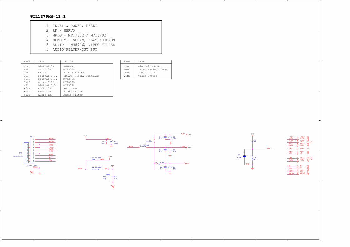
1 INDEX & POWER, RESET
DEVICE
SDRAM, Flash, VideoDAC
Servo 3.3V
RF 5VServo 5V
TCL1379M6-11.1
SUPPLY
VGNDDigital 3.3V
AVCC
5 AUDIO - WM8746, VIDEO FILTER
AV33
NAME
6 AUDIO FILTER/OUT PUT
AGND
4 MEMORY - SDRAM, FLASH/EEPROM
V25
Video Ground
Video FILTERAudio DAC
RVCCVCC
2 RF / SERVO
Audio filter
+5VA
NAME
Digital 2.5V
GND
Audio 12V
TYPE
SGND
V33 Digital 3.3VPICKUP HEADER
+12V
MT1379EMT1379E
Digital 5V Digital GroundMT1336E
MT1379EAudio 5VVideo 5V
DV33
+5VV
TYPE
3 MPEG - MT1336E / MT1379E
AVCC
GND
AV33
AV33
URST
V25
SGND
+P12V
URST
DV33
VCCRVCC
-P12V
-P12V+P12V
+PS5V
-24V
PCON
F-F+
VCC
+PS5V
SGND
GND
DV33+P33V
+P33V
AVCC
F+-24V
F-
PCON
VCC
+PS5V
MIC/HR
MIC/HL
MIC/HLMIC/HR
RVCC
-P12V [ 5 ]
GND [ 2,3,4,5 ]
+P12V [ 5 ]
AV33 [ 2 ]
VCC [ 2,3,4,5 ]
V25 [ 2 ]
AVCC [ 2 ]
DV33 [ 2,3, ]
RVCC [ 2 ]
SGND [ 2,3,4,5 ]
+PS5V [ 2 ]
URST [ 2 ]
V25
F- [ 2 ]F+ [ 2 ]-24V [ 2 ]PCON [ 2 ]MIC/HL [ 5]MIC/HR [ 5 ]
AV33 DV33
DV33
AVCC
VCC
RVCC
+C7220u
C80.1u
C30.1u
L4 FB AXIAL
+C2220u
D1
1N4148
12
CN1
CON15 2.5mm
123456789
101112131415
R14.7k
C10.1u
L1FB / 0805
+C510u
CN1
CON12 2.5mm
123456789
101112
C60.1u
Q1 8050
+C4220u
L2 FB AXIAL
+C9100u
+
C10220uC11
0.1u
L3 FB / 0805