circuit design for a 2.2 gbyte/s memory...
TRANSCRIPT

Circuit Design for a 2.2 GByte/s MemoryInterface
Stefanos Sidiropoulos
Work done at Rambus Inc with A. Abhyankar, C. Chen, K.Chang, TJ Chin, N. Hays, J. Kim, Y. Li, G. Tsang, A. Wong,
D. Stark
Increasing Chip I/O Bandwidth
Computers:Main memory:
SDRAM100 (100 Mbps) RDRAM (0.8-1.1 Gbps)
Peripherals:PCI (66 Mbps) Infiniband (2.5 Gbps)
Networks:Physical Front End:
LAN: Fast-Eth (100 Mbps) Gigabit-Eth (1Gbps)
WAN: OC-12 (625 Mbps) OC-48 (2.4 Gbps)
Switch Fabric:625 Mbps 2.5 Gbps
Outline
OverviewTiming Methods
Signaling Methods
Timing Circuits
Signaling Circuits
Results
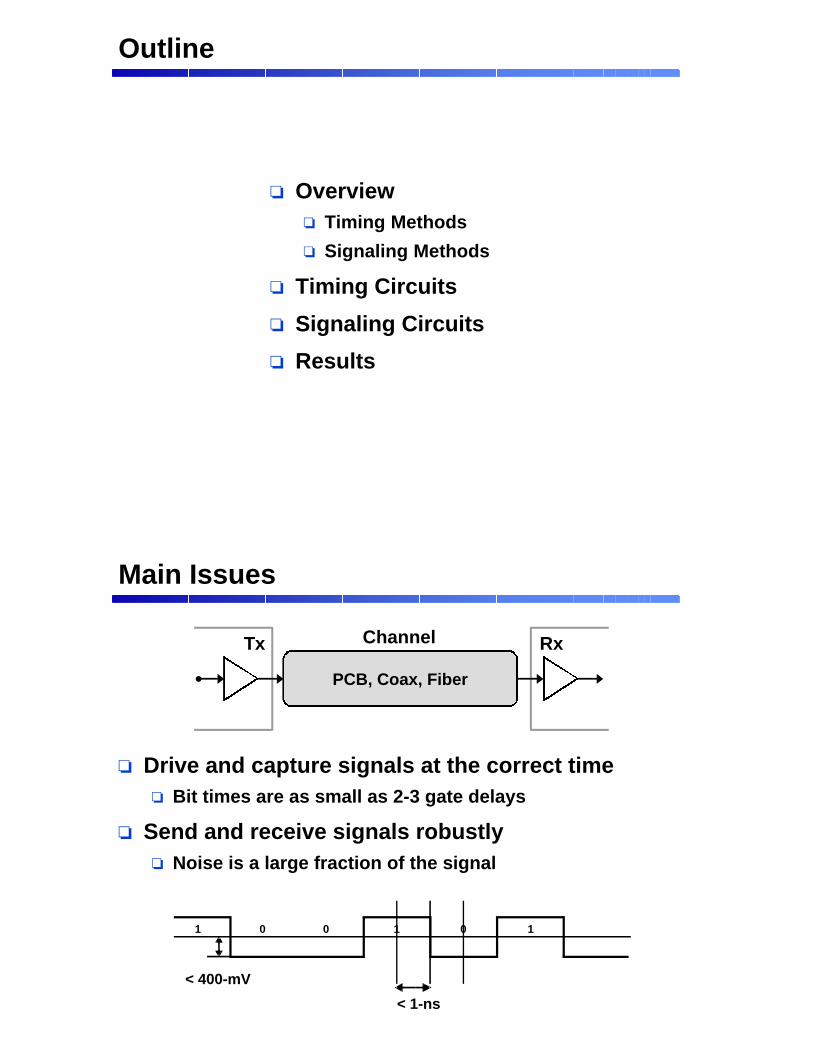
Main Issues
Drive and capture signals at the correct timeBit times are as small as 2-3 gate delays
Send and receive signals robustlyNoise is a large fraction of the signal
Tx RxChannel
PCB, Coax, Fiber
< 400-mV
< 1-ns
1 0 0 1 0 1

Timing Architectures
Synchronous:
Same frequency and phaseConventional busses
Conventional Memories
Mesochronous:
Same frequency, unknownphase
Fast memories/busses
MP networks
Interconnection networks
Plesiochronous:
Almost the same frequencyNetwork front-end
Router core
t t
F0
tA tB
F0tA≠≠≠≠ tB
F1 F2F1≈≈≈≈ F2
Synchronous Systems
On-chip clock is a multiple of system clock:
Synthesize on-chip clock frequency
On-chip clock phase varies:
Cancel clock buffer delay
PLL/DLLCKX
CKC
DI
CKX
DI
CKC
on-chip logic

Mesochronous Systems
Position on-chip sampling clock at the optimal point i.e. maximize “timing” margin
PLL/DLL
ref
data
CKSRC
rcvr
logic
CKRCV
CKSRC
data
CKRCV
D0 D1 D2 D3
Plesiochronous Systems
Recover incoming data fundamental frequency
Position sampling clock at the “optimal” point
DIN
CRC
CKR
rcvrlogic D0 D1DIN
CKR
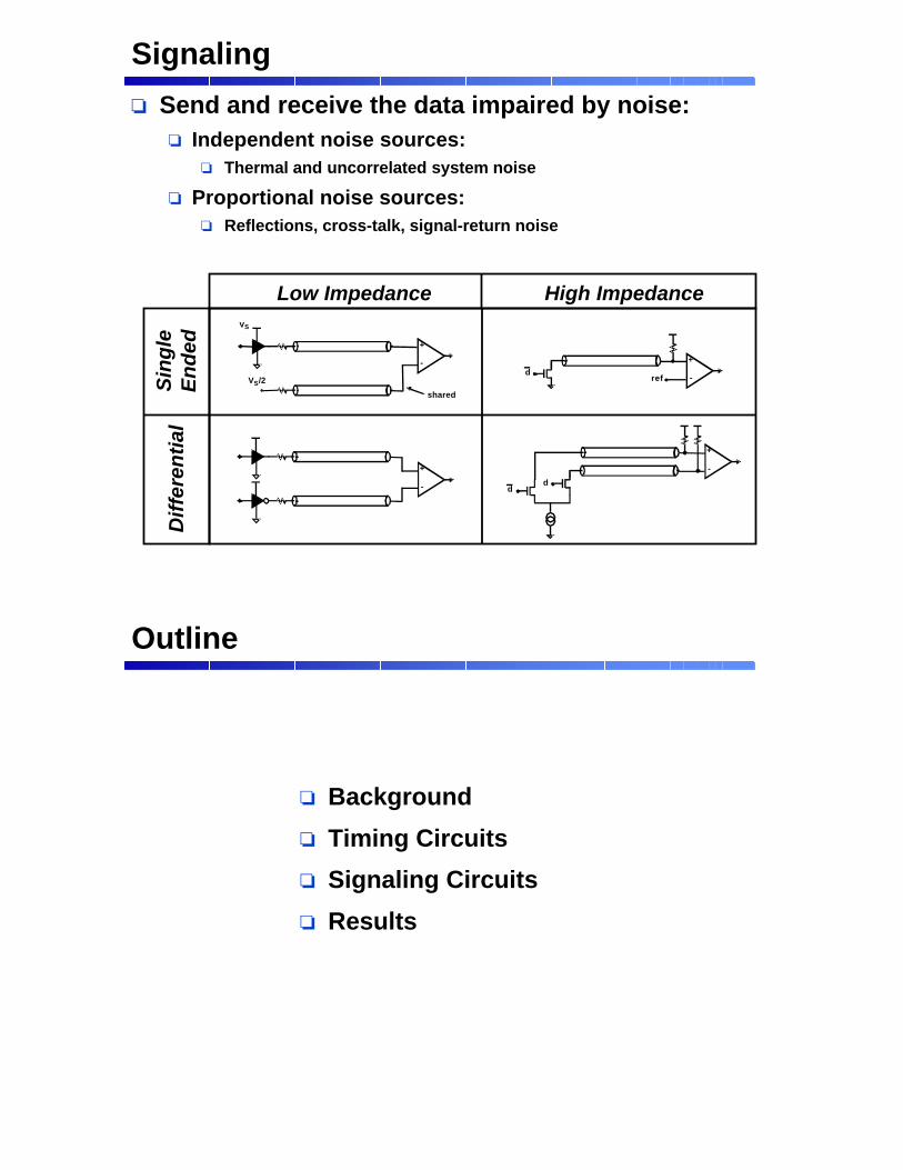
Signaling
Send and receive the data impaired by noise:Independent noise sources:
Thermal and uncorrelated system noise
Proportional noise sources:Reflections, cross-talk, signal-return noise
+
-
+
-
VS
VS/2
shared
+
-refd
+
-
dd
High Impedance
Dif
fere
nti
alS
ing
leE
nd
ed
Low Impedance
Outline
Background
Timing Circuits
Signaling Circuits
Results

Rambus Memory Channel
1.6-GB/s (800 Mbps/pin):Current mode signaling
Source synchronous clocking
M1 M2 M16
24
ClkGen
M1 M2 M16
Controller
D0 D1 D2
CTM
CFM
Increasing System Performance
Increase transfer rate:System Clock: 400 533 MHz (800 1066 Mbps/pin)
Peak Bandwidth: 1.6 2.2 GB/s
Challenges:
Timing MarginDevice Variations
Channel Imperfections
Voltage ErrorsBus Hand-off

Prototype DRAM Interface Chip
Technology: 0.25-µµµµm, 2.5-V CMOS
Supply: 1.8-V
Active Area: 11.2 x 1.3 mm2
Package: LGA, µµµµBGA
Chip Includes:
T/R DLL
2-Data bytes, 1-Address byte
Packet Protocol Logic
18 KB SRAM
Outline
Background
Timing CircuitsRequirements
Architecture
Timing Error Sources
Signaling Circuits
Results

RDRAM Timing Circuit Requirements
CFM
DQ/RQ
RCLK
D0 D1 D2 D3
CTM
DQ
TCLK
D0 D1 D2 D3
DLL
DQA DQBRQCTM CFM
TCLK RCLK RCLK TCLK RCLK
8 8 8
PLLs vs DLLs
Second/third order loop:
Stability is an issue
Frequency synthesis easy
Ref. Clk jitter gets filtered
Phase error accumulates
First order loop:
Stability guaranteed
Frequency synthesis problematic
Ref. Clk jitter propagates
Phase error does not accumulate
÷N
PDrefclk
VCO
Filter
PDrefclk
VCDL
Filter
clk
clk

Supply Noise: DLL vs PLL
No need for clock multiplication use a DLL
* Supply sensitivity: 0.1%-delay/%-supply/element
phaseerror(deg.)
time (ns)0 500 1000 1500
-50
-40
-30
-20
-10
0
DLLPLLBW 20MHzPLLBW 5MHz
DLL-pk
PLL-pk
6-stage DLL vs 6-stage PLL
Conventional DLL
Limited phase acquisition rangeGenerate delay by using phase interpolation
PD
refclk
clk

Variable Phase Interpolation
If φφφφ,,,, ψψψψ selectively span 2ππππ:
Can generate any ΘΘΘΘ
φφφφ,,,, ψψψψ can be generated by a DLL
φφφφ’
ψψψψ’
φφφφ
ψψψψ
ΘΘΘΘ
w = 0..N
NwwN ψψψψφφφφ
ΘΘΘΘ⋅⋅⋅⋅++++⋅⋅⋅⋅−−−−
====)(
ψψψψ0000ψψψψ1111
ψψψψ2222 ψψψψ3333
φφφφ0000
φφφφ1111
φφφφ2222
φφφφ3333
φφφφ ψψψψ
RDRAM Delay Buffers
Use differential elements with replica biasing:Increased noise immunity
Not easily portable
Require larger supply head-room but ok for 1.8-V
BiasCircuit
VCTL
VCN
VCP
[Hu’92]
[Maneatis’93]

Interpolator Design
Interpolator bias and input/output time constant scales
TDC remains linear over large frequency range
+
-
5DAC
VCN
VCP
Dual DLL Block Diagram
AmpAmp
PD/CP/Bias
PDup/dn
InputClock
Ref Clock
CORE
PERIPHERAL
FSM

Device Timing Variations
100 parts: µµµµ ≅≅≅≅ 30-ps, σσσσ ≅≅≅≅ 20-ps
Receive Window Distribution
0
5
10
15
20
25
-50 -40 -30 -20 -10 0 10 20 30 40 50 60 70 80 90 100
Receive-valid Window Center (ps)
# p
art
s
Propagation Delay Mismatch
Clock and data channels different
Clock and data spectral components different
Propagation delays can differ by ~ 100-ps
Regain margin: every DRAM transmit/receivetiming must be offset from its lock point
Discontinuity
φφφφ
DRAM
)]2sin()[sin()( ϕϕϕϕωωωωωωωω −−−−⋅⋅⋅⋅⋅⋅⋅⋅++++⋅⋅⋅⋅⋅⋅⋅⋅==== trtAtv)sin(')( θθθθωωωω ++++⋅⋅⋅⋅⋅⋅⋅⋅====⇒⇒⇒⇒ tAtv
2φθ
A’
A
rA
Module

Original Dual-DLL
AmpAmp
PD/CP/Bias
Mux+Interpolator
PD
Counter
Decoder
up/dn
FBClock
InputClock
8
MainClock
to I/O
Ref Clock
FSM
DLL for “in-system” Calibration
AmpAmp
PD/CP/Bias
Mux+Interpolator
PD
Counter
Decoder
up/dn
FBClock
8
Mux+Interpolator (_2)Decoder
Adder
8
Offset[7:0]
MainClock
to I/O
Ref Clock
InputClock
(set @boot time)

Outline
Background
Timing Circuits
Signaling CircuitsBus Environment Challenges
Output Subsystem Design
Results
“Back-to-Back” Reads
Compliance voltage for M2 as low as 0.5-V
2 ∆∆∆∆t2Mem2
Controller ∆∆∆∆t1+∆∆∆∆t2 2 ∆∆∆∆t2
Contr.
Mem1 Mem2
∆∆∆∆t2∆∆∆∆t1
Vterm
Vterm
Vterm-Vsw
Vterm-1.5Vsw

Output Driver Subsystem
_7
Q0
DQ0
_7
Q1
DQ1
_7
Q8
DQ8
+
-
CC[6:0]EN
_7
VG[6:0]
Driver BiasVoltage
Generator
VGREF
VGATE
77
Driver Bias Voltage Generator
Constant gate overdrive:Increase noise immunity
Constant saturation margin over PVT
IRIC
>>>>VT
IR����R
VGREF
R

Driver IV Characteristics
0
5
10
15
20
25
30
35
0 0.2 0.4 0.6 0.8 1 1.2 1.4 1.6 1.8
Vpad (V)
Iou
t (m
A)
TT
SS
FF
Output Driver Model
Negative resistance compensates for finite ro
omoogmout vgArvvgi ⋅⋅⋅⋅⋅⋅⋅⋅−−−−++++⋅⋅⋅⋅==== 2/
gm
-A
gm2
vG
vO
ro

Output Driver Schematic
M6-M7 control maximum feedback current
M3/M4 ratio constrained to minimize time constant
VG[6:0]
DQ
M1[6:0]
M2[6:0]
QM3 M4
M5
M6[1:0]
M7[1:0]SL[1:0]
Driver IV Characteristics
0
5
10
15
20
25
30
35
0 0.2 0.4 0.6 0.8 1 1.2 1.4 1.6 1.8
Vpad (V)
Iou
t (m
A)
TT
SS
FF
Outline
Introduction
Timing
Signaling
Results
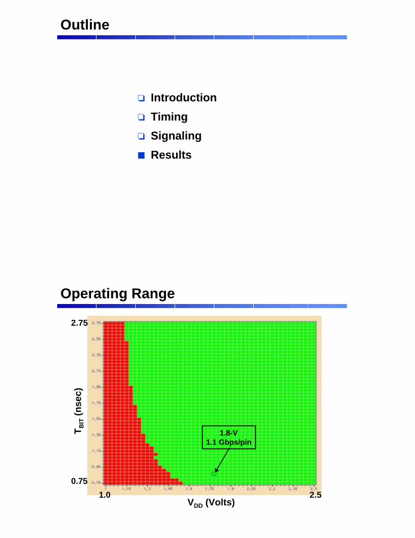
Operating Range
VDD (Volts)
TB
IT (
nse
c)
1.0 2.5
0.75
2.75
1.8-V1.1 Gbps/pin

Measured DLL Jitter
< 100-ps peak-peak with interface and core active
Uncalibrated Output Data-valid Window
TBIT = 900-ps, TOFFS = default TQ offset ~ 150-ps
760-ps
1-V
-1.0 1.0∆∆∆∆t (ns)
1.5
VD
D (
Vo
lts)
2.5

Calibrated Output Data-valid Window
TBIT = 900-ps, calibrated TOFFS TQ offset < 20-ps
780-ps
1-V
VD
D (
Vo
lts)
-1.0 1.0∆∆∆∆t (ns)
1.5
2.5
Measured Calibration Accuracy
DNL, INL < 2-LSB
0
50
100
150
200
250
300
350
0 50 100 150 200 250code #
off
set
(deg
rees
)
400 MHz
533 MHz

RDRAM Power Modes
DLL must go into low-power “nap” mode
IVDD < 4-mA
Restore clock phase within 80-ns
Digital peripheral loop logic naturally holds state
Hold state of core loop on 25-pF charge-pump capacitor
Measured Driver I-V Characteristics
0
5
10
15
20
25
30
35
0 0.2 0.4 0.6 0.8 1 1.2 1.4 1.6 1.8
Vpad (V)
Iou
t (m
A)
FB off
FB on
Summary
Increasing memory interface bandwidth: Minimize both voltage and timing errors:
Voltage errors are systematic
Compensated with new driver design
Timing Errors are unpredictable
Compensated with “in-system” calibration
Expect to see more digital “calibration” in high speed links:
Challenge is minimize overhead:Area, Power, Yield..
System bring-up and ease of use..