circuit and cad techniques for expanding the sram design space
TRANSCRIPT

Robust
Low
Power
VLSI
Circuit and CAD Techniques for
Expanding the SRAM Design Space
PhD Proposal
Jim Boley
April 24, 2013

Power Limits Across the Application Space
2
Po
wer
Performance
Medical devices,
Microsensors:
Energy Constrained Portable Electronics,
Ambient Intelligence:
Workloads vary;
Maximize lifetime
High Performance Apps: Performance Driven
Power density

Energy Efficiency Across the Application Space
3
Po
wer
Performance
Medical devices,
Microsensors:
Energy Constrained Portable Electronics,
Ambient Intelligence:
Workloads vary;
Maximize lifetime
Static random access memory (SRAM): Energy efficient design across the space
Performance limited
Reliability limited

Why Focus on SRAM?
4
High speed, high density memory option
Consumes large amounts of die area
High leakage energy
Often sets minimum operating voltage (VMIN)
Memory access performance bottleneck
www.intel.com
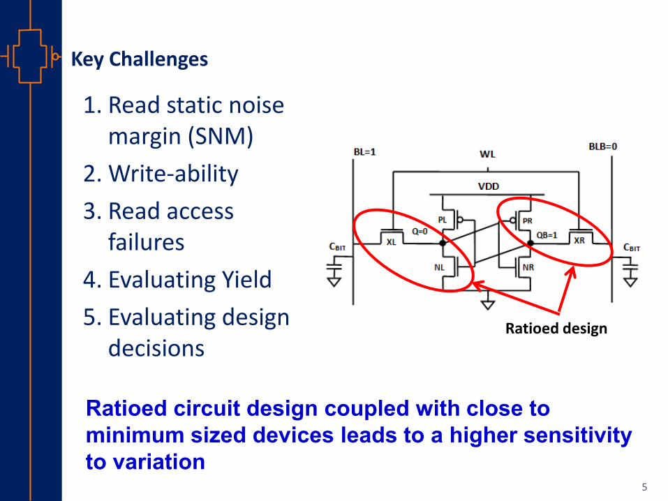
Key Challenges
5
1. Read static noise margin (SNM)
2. Write-ability
3. Read access failures
4. Evaluating Yield
5. Evaluating design decisions
Ratioed design
Ratioed circuit design coupled with close to
minimum sized devices leads to a higher sensitivity
to variation

Thesis Statement
By developing a set of methods and tools for evaluating SRAM design tradeoffs, we can push SRAM designs to lower operating voltages, increase yields, and evaluate both circuit and architectural design decisions.
6

Outline
Motivation
Sub-threshold SRAM design
Analysis of sub-threshold bitcell and assist methods
A method for evaluating dynamic VMIN
Extending the capabilities of ViPro
A canary based feedback system for PVT tracking
Schedule
7

Input signals are low frequency (low clock speed)
Highly energy constrained
Goal: run solely off harvested energy (10’s of μWs)
Information
Assessment,
Treatment
8
Motivation for Sub-VT in Body Sensor Networks
Sub-threshold operation minimizes energy per
operation

Challenges: Sub-Threshold SRAM
Familiar Problems
Hold SNM, Read SNM, Write NM
New Problems:
Reduced Ion/Ioff ratio (Read access failure)
Exaggerated VT variation impact (Ion varies exponentially with Vt)
Possible Solutions
Read SNM: Use a read buffer to decouple the data
Write NM: Use write assist (Boosted WL/Negative BL VSS)
Research Question: How can we design an ultra low power SRAM capable of reliable
operation at an operating voltage of 500 mV and a frequency of 200 KHz?
Research Question: How can we design an ultra low power SRAM capable of reliable
operation at an operating voltage of 500 mV and a frequency of 200 KHz?
9

10
Po
wer
Performance
Medical devices,
Microsensors:
Energy Constrained Portable Electronics,
Ambient Intelligence:
Workloads vary;
Maximize lifetime
Sub-Threshold Design
Scope
High Performance Apps: Performance Driven
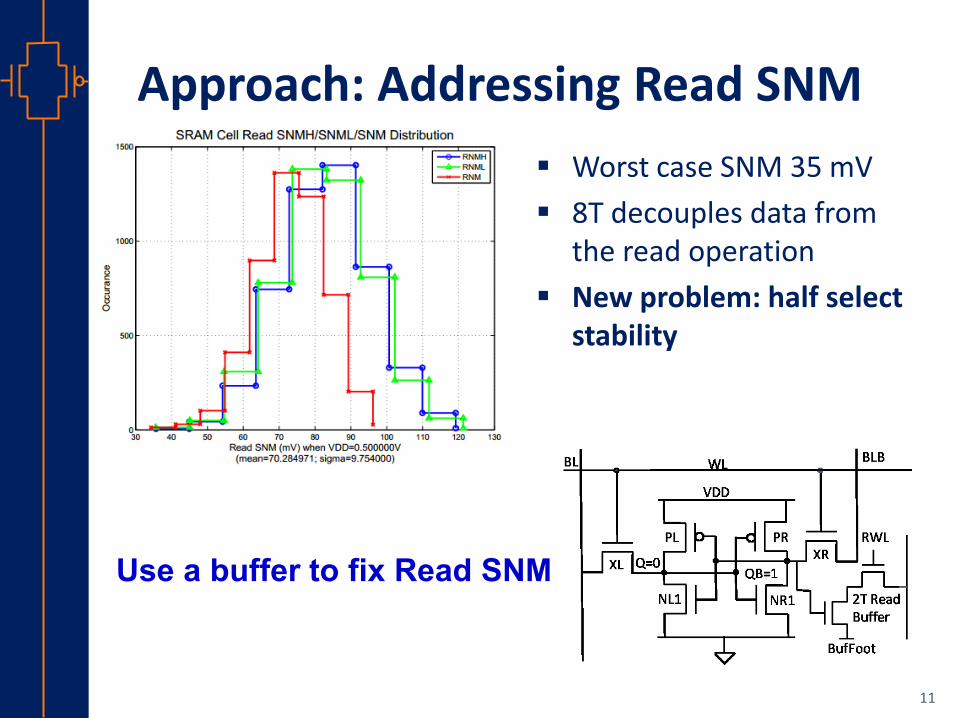
Approach: Addressing Read SNM
11
Worst case SNM 35 mV
8T decouples data from the read operation
New problem: half select stability
Use a buffer to fix Read SNM

Approach: Addressing Half Select
12
Both data and instruction memory used as FIFO
Memory written once every 8 cycles
[R. Houle, VLSI Circuits 2007]
Word0 Word7
Data In<15:0> Column Address
Row Buffer
SRAM Block
Data In<127:0>
Use a row buffer to prevent half select instability

Approach: Addressing Write-ability
13
Write-ability dependent on N/P current ratio
RVT devices high N/P ratio in sub-vt
Downside: 22x increase in leakage per bitcell
Use regular VT devices to ensure write-ability

Approach: Addressing Read Access
14
Boost read footer to prevent read access failures
Boost unaccessed footers to
VDD
Boost unaccessed footers to
VDD
[N. Verma, JSSC 2008]

Metrics for Evaluation
1. Minimum operating voltage at which reliable operation is achievable
Success: reliable operation at 500 mV and 200 KHz
2. Total energy per access
Success: 10’s picojoules range
15

Contributions
Methodology for designing embedded Sub-VT SRAMS
Reliable operation from 0.3V – 0.7V at 200 KHz
Energy per access 12.1 pJ
Leakage per cycle 6.6 pJ
16
Future work: reduce leakage per cycle by using
high VT devices
[Zhang, JSSC 2013]

Outline
Motivation
Sub-threshold SRAM design
Analysis of sub-threshold bitcell and assist methods
A method for evaluating dynamic VMIN
Extending the capabilities of ViPro
A canary based feedback system for PVT tracking
Schedule
17

Motivation for Sub-threshold SRAM
Motivation: Reduction in leakage power
Quadratic active energy savings
Challenges: Increased sensitivity to variation
Reduced Ion/Ioff ratio
Read Static Noise Margin
Write-ability
Read access stability
Approaches: Alternative bitcell designs
Read and write assist methods
18

Hypothesis
By testing different combinations of bitcell topologies and assist methods, we can determine which approach results in the largest reduction of read and write VMIN over the nominal case (6T bitcell with no assist methods).
19

20
Po
wer
Performance
Medical devices,
Microsensors:
Energy Constrained Portable Electronics,
Ambient Intelligence:
Workloads vary;
Maximize lifetime
Sub-Threshold Design
Scope
High Performance Apps: Performance Driven

Approach:Non-6T Cell for Read Stability
[J. Kulkarni, JSSC’07]
Schmitt-trigger (ST-cell)
TL
PL
NL
TR
PR
NR1
NR2
NF VDD
WL
BLB BL
WWL
[J. Boley, JLPEA 2012]
10T Schmidt trigger (ST) cell: 1.56x increase in read SNM of 6T at 33% area penalty
8T asymmetric ST cell: 19% higher RSNM than 10T ST due to single ended reading structure

Assist methods
Write Assist methods Read assist methods
22
WL Boost Strengthens passgate device
Con: half select instability
Negative BL Strengthens passgate device
Cons: generating negative voltage, increase BL leakage during write
1. WL Boost Increases Ion faster reads
Con: reduces RSNM
2. Negative WL VSS- Decrease Ioff reduces BL
leakage current
3. CVDD boost and CVSS droop Increase the read static noise
margin of the cell

Metrics for Evaluation
1. Reduction in Read and Write VMIN compared to the nominal case (6T bitcell with no assist methods)
23

Results
24
SRAM write limited Write VMIN: 620 mV
Read VMIN : 440 mV
BLVSS reduction: largest reduction of write VMIN
WL VSS and CVSS: largest improvement on read VMIN Bitline leakage was a major
contributor to reduced read margin
Impact of assist methods > impact of bitcell topologies on reducing VMIN
1 6 11 160
5
10
15
20
25
30
35
Asym ST
10T ST
6T
8T
% R
edu
ctio
n i
n R
ead
V
MIN
CVDD CVSS WLVDD WLVSS
Cu
mu
lati
ve
Dis
trib
uti
on
1 20
5
10
15
20
25
30
6T
8T
10T ST
Asym ST
% R
edu
ctio
n i
n W
rite
VM
IN
BLVSS WLVDD
[J. Boley, JLPEA 2012]

Outline
Motivation
Sub-threshold SRAM design
Analysis of sub-threshold bitcell and assist methods
A method for evaluating dynamic VMIN
Extending the capabilities of ViPro
A canary based feedback system for PVT tracking
Schedule
25

Motivation Static stability metrics are optimistic for write
Assumes infinite pulse width
Doesn’t account for transient behavior
Upside: shorter simulation times
Need dynamic metrics for more accurate prediction of VMIN
Current metric is TCRIT the critical or minimum WL pulse width required
to write the bitcell
Scope: Focus on dynamic write-ability
Problem: determining the dynamic write margin of the worst
case cell in large (i.e. > 1 Mb) memories requires a
prohibitively large number of Monte Carlo (MC) simulations
26

27
Po
wer
Performance
Medical devices,
Microsensors:
Energy Constrained Portable Electronics,
Ambient Intelligence:
Workloads vary;
Maximize lifetime
Full range of design space
Scope
High Performance Apps: Performance Driven

Prior Art
[A. Singhee, DATE, 2007]
Analytical models Less accurate
Curve fitting Dynamic margin does not
closely match any known distribution
Statistical blockade Run initial simulation
Create tail classifier
Generate MC points
Simulate only samples classified as tail points
28

How can we improve statistical blockade?
Downsides to statistical blockade:
Calculating the worst case dynamic margin in a 100 Mb array using recursive statistical blockade requires over 894,000 total Monte Carlo simulations
Hypothesis: using sensitivity analysis, we can
further reduce the time required to calculate
dynamic VMIN

Approach: Sensitivity Analysis
6σ 3σ 0σ 3σ 6σ Stronger VT Offset Weaker
Sweep VT of each transistor to calculate ΔTCRIT / ΔVT
Sweep VT of each transistor to calculate ΔTCRIT / ΔVT
Bitcell Netlist
Run VT vs. Tcrit simulation
Polynomial Curve Fitting TCRIT-OFFSET = ax3+bx2+cx+d,
x = VT-Shift
Generate VT distribution (e.g. in MATLAB)
Compute TCRIT = TCRIT-NOM + TCRIT-PUL-OFFSET
+…+ TCRIT-PGR-OFFSET
Repeat for N iterations
[J. Boley, DATE 2013]

Metrics for Evaluation
1. Speedup gained over statistical blockade (SB)
2. Loss of accuracy compared to SB
31

Results: Accuracy Comparison between the worst case bitcell as
predicted by statistical blockade and sensitivity analysis
Across VDD, the sensitivity analysis results match closely to the statistical blockade data
The worst case percent error is 6.83% while the average is ~3%
Modeled data vs. Statistical Blockade (Percentage Error)
500 mV 600 mV 700 mV 800 mV 900 mV 1000 mV Average
100K 6.83 2.96 -0.18 0.83 -4.50 -2.72 3.01
10M -4.25 -3.69 -2.64 -0.70 0.83 -2.20 2.39
100M 6.51 5.61 4.75 1.21 1.43 -2.27 3.63

Sensitivity analysis provides a 112.5x speed up over recursive statistical blockade with an average percentage error of ~3% Sensitivity analysis provides a 112.5x speed up over recursive statistical blockade with an average percentage error of ~3%
Statistical
Blockade
Sensitivity
Analysis
Num.
simulations Run Time
Initial
Simulation 24,000 18.8 min
100 Kb 107,904 0.72 s
10M 531,096 72 s
100M 231,288 12 min
Total
Simulations 894,288
Total Run
Time 60 Hours 32 minutes
Results: Speedup

Outline
Motivation
Sub-threshold SRAM design
Analysis of sub-threshold bitcell and assist methods
A method for evaluating dynamic VMIN
Extending the capabilities of ViPro
A canary based feedback system for PVT tracking
Schedule
34

Motivation
SRAM’s face many design challenges in nanoscale technologies: Increased variability Higher leakage Longer interconnect delay
SRAM limits SoC VMIN 6T bitcell limited by reduced margins Increasing memory capacities
New knobs have been introduced: Assist methods Alternative bitcells Offset compensated sense amps
Evaluation of circuit and architectural design decisions in terms of global figures of is difficult without creating a full design
35

Problem Statement
Without the proper support structure and tools, it would be nearly impossible to re-design and re-optimize an entire memory by hand every time we try a new circuit, much less explore a technique’s impact across different technologies and applications
36

37
Po
wer
Performance
Medical devices,
Microsensors:
Energy Constrained Portable Electronics,
Ambient Intelligence:
Workloads vary;
Maximize lifetime
Super-Threshold Design
Scope
High Performance Apps: Performance Driven

Prior Art
38
ViPro (developed by Satya Nalam):
Tase: technology agnostic simulation environment Uses simulation templates for
characterizing SRAMs across technology nodes
Hierarchical memory model Easily extensible and scalable
Faster than running full simulation
Brute force optimization Supports optimization of a single
bank SRAM design
Knobs: number of rows and columns
Metrics: energy and delay

Hypothesis
By extending the existing ViPro tool we will be able to explore a much larger design space and run a much larger set of novel experiments which will allow for reductions in SRAM VMIN, increases in yield and a better understanding of design tradeoffs.
39

Approach Overview
40
Existing Tool:
Designs: single bank
Bitcell type: 6T
Metrics: Energy and delay
Optimization: Brute Force
Proposed Additions:
Designs: multi-bank, read and
write assist methods
Bitcell type: 8T
Metrics: Yield & Area
Optimization: Simulation
optimization

Justifying Our Approach Multi-bank: Single bank designs are limited to <100 Kb Current trend larger capacities
8T: Commonly used in L1 cache Single ended sensing creates new challenges
Read and write assist methods: 6T reaching its fundamental limits due to technology
scaling Assist methods offer new design tradeoffs Choose 2 write assist methods and 2 read assist
methods to evaluate
41

Justifying Our Approach
Yield evaluation:
Larger designs and higher variability lead to reduced yields
Clear need to be able to evaluate the effectiveness of new circuit techniques on improving yield
Use existing techniques for yield evaluation
Area evaluation:
Key feature of SRAMs is high density
42

Justifying Our Approach
Circuit and architecture co-optimization:
Architectural changes affect the optimal circuit level parameters (sizing, number of buffer stages, etc.)
Brute force only works for small optimization space
Proposed additions greatly expand the design space
Need an optimization engine that can reduce the number of iterations by making smart choices about which knobs to turn
43

Evaluation Metrics
Difficult to make direct comparison to existing tools like CACTI CACTI is an tool for high level design space exploration,
however it optimizes at the architecture level only
Uses ITRS parameters for evaluating across technologies which may not lead to accurate assessments
Proposed metrics for evaluating the tool: What novel contributions are necessary for creating the tool?
What are the novel experiments that the tool enables?
Metric for evaluating the optimization engine: Total speedup compared to brute force optimization
44

Anticipated Contributions
Tool for rapid SRAM design space exploration
Circuit and architecture co-optimization engine
45
Subset of Anticipated Experiments How do assist methods affect read access yield?
What are the tradeoffs in terms of the global figures of merit between the assist methods?
What affect does an offset compensated sense amplifiers have on yield and read access time?
What is the most limiting factor in terms of yield and how does that change with technology scaling?
Outline
Motivation
Sub-threshold SRAM design
Analysis of sub-threshold bitcell and assist methods
A method for evaluating dynamic VMIN
Extending the capabilities of ViPro
A canary based feedback system for PVT tracking
Schedule
46

Motivation Typical commercial
designs must guard band for a range of process, temperature, voltage (PVT) corners
Guard banding must be done pre-fabrication to ensure reliability across all corners
47
Problem: Conservative guard banding eliminates potential
post-fabrication energy savings.
Loss in potential energy savings Loss in potential energy savings
[Wang, JSSC 2008]

Prior Art- Canary Feedback System
48
Previously applied to data retention voltage (DRV)
Canary cells designed to fail at regular intervals
Canary cells use upsized transistors to reduce local mismatch
Closed loop controller detects canary failures
Direct tradeoff made between reliability and power
VCTRL
6T Bitcell
Virtual VDD
Canary Cell
[Wang, JSSC 2008]
Previously reported: 30x power
savings over conservation guard
banding [Wang, JSSC 2008]

Hypothesis
We can achieve significant power savings over conservative guard banding by using a canary based feedback system to reduce write VMIN
49
NOTE: While a full canary system would need to
also consider the read path, we have chosen to
limit our scope to only the write operation in this
work.

50
Po
wer
Performance
Medical devices,
Microsensors:
Energy Constrained Portable Electronics,
Ambient Intelligence:
Workloads vary;
Maximize lifetime
Super-Threshold Designs
Scope
High Performance Apps: Performance Driven

Approach: Canary Design
Boost BL VSS above ground
Keep WL pulse width equal to core array
Lower voltage until failures are detected
Challenge: setting the BLB voltage
51
BL=1
PUL
PDL
PUR
PDR
PGL PGR Q= 0 QB=1
WL
CVSS
CVDD
BLB=25 mV, 50 mV, 75 mV, 100 mV BLB=25 mV, 50 mV, 75 mV, 100 mV

Preliminary Testing
0 10 20 30 40 50 60 70 80 90 100840
860
880
900
920
940
960
980
BL VSS Voltage (mV)
VM
IN (
mv)
52

Approach: Other Canary Designs to Consider
Reverse Assist Methods:
Droop WL VDD: Reduce the strength of the passgate transistors
Negative CVSS: Increase the strength of the cross coupled inverters
Boosted CVDD: Increase the strength of the cross coupled inverters
Shorten write wordline (WL) pulse width: Shorter pulse width higher failure voltage
53
Scope: choose one or two of these methods for
implementation on a test chip

Approach: Control Loop
54
Write bitcell to ‘0’ under nominal
conditions
Write bitcell to ‘0’ under nominal
conditions
Yes No
No
Apply reverse assist method, write a ‘1’
into the cell
Apply reverse assist method, write a ‘1’
into the cell
Non-tolerable failures
detected?
Raise VDD Raise VDD
With reverse assist applied, write a ‘0’
into the cell
With reverse assist applied, write a ‘0’
into the cell
Lower VDD Lower VDD
Non-tolerable failures
detected?
Yes
No

Anticipated Contributions
Canary design that tracks PVT variation and fails at specified intervals
Control system that can regain energy lost due to conservative guard banding by further lowering write VMIN
55

Schedule Project Milestone Status/Target
BSN Sub-VT SRAM Rev. 1- Design/layout/testing Completed Rev. 2- Design/layout Completed Rev 2: Chip Testing August-2013
Dynamic Write VMIN Estimation Create/verify model Completed Sub-threshold bitcell analysis Test Chip Completed
Virtual Prototyping Tool
Support multi-bank design Completed Support for 8T bitcell Completed Verify Model Accuracy July-2013 Integrate two read and two write assist features
September-2013
Integrate area estimation December 2013
Integrate yield estimation April 2014 Optimize using simulation optimization algorithm
August-2014
Canary Feedback System
Evaluation of canary design December 2013
Design of voltage control loop February 2014
Simulation/Verification/Layout April 2014
Chip Testing December 2014
Write up Thesis Writing February-2015
56

Publications 1. F. Zhang, Y. Zhang, J. Silver, Y. Shakhsheer, M. Nagaraju, A. Klinefelter, J. Pandey, J. Boley,
E. Carlson, A. Shrivastava, B. Otis, and B. H. Calhoun, “A Battery-less 19μW MICS/ISM-Band Energy Harvesting Body Area Sensor Node SoC,” ISSCC, February 2012.
2. J. Boley, J. Wang, and B. H. Calhoun, “Analyzing Sub-Threshold Bitcell Topologies and the Effects of Assist Methods on SRAM VMIN”, JLPEA, April 2012.
3. Y. Zhang, F. Zhang, Y. Shakhsheer, J. Silver, A. Klinefelter, M. Nagaraju, J. Boley, J. N. Pandey, A. Shrivastava, E. J. Carlson, A. Wood, B. H. Calhoun, and B. Otis, “A Batteryless 19 µW MICS/ISM-Band Energy Harvesting Body Sensor Node SoC for ExG Applications,” JSSC, 2013.
4. J. Boley, V. Chandra, R. Aitken, and B. Calhoun, “Leveraging Sensitivity Analysis for Fast, Accurate Estimation of SRAM Dynamic Write VMIN,” DATE, 2013.
5. J. Boley, P. Beshay, B. Calhoun, “Virtual Prototyping (ViPro) Tool for Memory Subsystem Design Exploration and Optimization,” TECHCON, 2013.
Anticipated publications: 1. SRAM Circuit and Architecture Co-Optimization 2. Subthreshold SRAM Design Featuring Low Energy Read operation 3. Evaluation of SRAM Assist Methods on Top Level Design Metrics 4. Optimization of SRAMs for Improved Yield 5. Using simulation optimization for SRAM design space exploration 6. Canary based closed-loop control system for optimizing write VDD
57

Acknowledgemetnts
Committee Members Ben Calhoun, Adviser
Joanne Dugan, Chair
Don Brown, Member
John Lach, Member
Ronald Williams, Member
Fellow Students Randy, Satya, Jiajing, Sudhanshu, Joe, Yousef, Kyle, Yanqing, Aatmesh,
Alicia, Seyi, Peter, Arijit, Chu, Patricia, Divya, Yu, He
ARM Research Vikas Chandra and Rob Aitken
58

Backup slides
59

Key Challenges: Estimating Yield
60
Monte Carlo (MC) = Gold Standard
>1 MB arrays make MC sims infeasible
Distributions not always normal
40 60 80 100 120 140 160 1800
50
100
150
200
250
300
Dynamic Retention Voltage (mV)(mean=87.446744; sigma=19.294505)
Occu
ran
ce
DRV Distribution

Key Challenges: Evaluating Design Decisions
61
Design Knobs: VDD
Banks/rows/columns Peripheral Circuit Topology
Bitcell Topology Read/Write assist methods
Metrics: Speed Power Area
Reliability
Variability
Leakage
Technology
Scaling
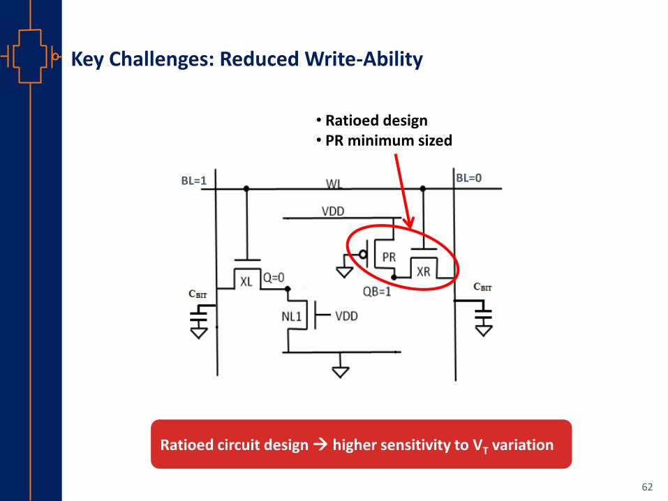
Key Challenges: Reduced Write-Ability
62
BL=1
• Ratioed design • PR minimum sized
BL=0
Ratioed circuit design higher sensitivity to VT variation Ratioed circuit design higher sensitivity to VT variation

Key Challenges: Read Access Stability
63
Goal: minimize TWL-SAE
IREAD determines ΔV
VOS input referred offset of the sense amp (SA)
Increased leakage also leads to reduced ΔV
Failure point: ΔV < VOS
[J. Ryan, ISLPED 2011]

Motivation of Sub-threshold (VDD<VT)
Sub-threshold benefits: VDD from [1.8,1.0]V to [0.4,0.2]V
Leakage Power Decreases: Power = VDD Ioff
VDD goes down: 2.5X to 9X
DIBL reduces Isub-threshold: 2X to 10X
Igate and IGIDL become negligible
Pleak: 5X to 90X
Energy Consumption Decreases Aging Effects Improve
Eactive = CVDD2 NBTI, EM, TDDB
Etotal/operation minimized in sub-VT
Main Limitations: Variation, Slow Speed
64

Approach: 8T Asymmetric Schmitt Trigger Bitcell
65
Uses single-ended reading and assymetric inverters similar to the 5T cell described in [Nalam, CICC’09] to increase read margin
Write operation similar to 6T write
Asymmetric ST cell achieves 86% higher static read noise margin (RSNM) than the 6T cell, and 19% higher RSNM than the 10T ST cell
10T ST
6T
Asym ST

Approach: Write Assist Methods Goal
Weaken pull-up FET
Strengthen pass-gate FET
Knobs Size pass-gate to pull-up ratio (not
efficient)
Collapse VDD to weaken PFET
Boost WL VDD
Cons: half selected cell stability
Reduce BLVSS
Cons: increased BL leakage
RWLon>VDD
BL<VSS
PG
PU
PD
VGSPG>VDD

Approach: Read Assist methods
Keys Increase Ion Reduce Ioff (BL leakage current in unaccessed cells)
Knobs
C. boosted
bitcell voltage D. negative
bitcell VSS
RWLoff<0
QB
RBL
B: negative off-WL A: boosted on-WL
Ioff
RWLon>VDD
QB
RBL
Ion [R. Mann, ISQED’10]

Approach: Verifying Assumptions
Experimental setup: Add variation to other five
transistors, sweep VT of single transistor
Repeat for each transistor
Expected output: Shape of the sensitivity curve
unchanged
Nominal value (0σ) shifted higher or lower
-0.2 -0.1 0 0.1 0.21
1.5
2
2.5
3
VT ShiftT
crit (
Norm
aliz
ed)
Nominal
6σ 3σ 0σ 3σ 6σ VT Offset

Approach: Sensitivity Analysis
Sweep VT of each transistor to determine sensitivity
Generating the VT curves requires only 1080 simulations
Once the VT curves have been generated, the Monte Carlo data can be run through the model, and the worst case bitcell can be quickly found
6σ 3σ 0σ 3σ 6σ Stronger VT Offset Weaker
BL=1
PUL
PDL
PUR
PDR
PGL PGR Q= 0 QB=1
WL
CVSS
CVDD
Use sensitivity analysis to calculate ΔTCRIT / ΔVT for each transistor
Use sensitivity analysis to calculate ΔTCRIT / ΔVT for each transistor
BLB=0

500 600 700 800 900 1000
101
102
103
104
105
VDDW
ors
t C
ase
Tcrit
100K
10M
100M
Applying Results to Dynamic VMIN
In order to calculate VMIN we can repeat the procedure for varying VDD
We chose 6 points from 0.5-1V
The plot shows the worst case bitcell for a given VDD, varying the array size
The curve represents the point of single bit failure, below the curve represents multiple failures, above the curve represents no failures
Failure Region
No failures

Applying Results to Assist Methods
Memory size is 1 Mb
Lower VDD shows negative WBL has clear advantage
ΔV = 100 mV for each assist method
500 600 700 800 900 1000
100
101
102
103
104
105
VDD
Wo
rst C
ase
Tcrit
CVSS Boost
Nominal
WWL Boost
Neg WBL
Negative BL reduction reduces the worst case TCRIT close to an order of magnitude more than WWL boosting at 500 mV
Negative BL reduction reduces the worst case TCRIT close to an order of magnitude more than WWL boosting at 500 mV

0 2 4 6 8-0.2
-0.1
0
0.1
0.2
0.3
0.4
0.5
0.6
Time (a.u.)
Vo
lta
ge
Q
QB
WWL
Negative BL strengthens pass-gate and pull-up devices
Negative BL strengthens pass-gate and pull-up devices
Advantage of Negative BL Reduction
Negative BL passes a stronger ‘0’ into the cell, effectively strengthening the PUL transistor and decreasing the write time. This gives negative BL an advantage over WWL boosting at lower VDD.
Negative BL passes a stronger ‘0’ into the cell, effectively strengthening the PUL transistor and decreasing the write time. This gives negative BL an advantage over WWL boosting at lower VDD.
BL=1 BLB=-100mV
PUL
PDL
PUR
PDR
PGL PGR
WL
CVSS
CVDD
QB=-0.1V
At 500 mV, the majority of write time is spent pulling Q high
At 500 mV, the majority of write time is spent pulling Q high

Project Summary
73
ViPro ViPro
Dynamic VMIN Dynamic VMIN
Bitcell and Assist Evaluation
Bitcell and Assist Evaluation
BSN Memory BSN Memory
Use VMIN model to evaluate yield
Canary Design Canary Design
How do assist methods affect global FoM’s
How do assist methods affect dynamic VMIN?
Which assist method to choose from?
Use of canaries to monitor reliability
What is the associated overhead of using canaries?