cient modeling of the nonlinear properties of
TRANSCRIPT

sensors
Article
Consistent and Efficient Modeling of the NonlinearProperties of Ferroelectric Materials in CeramicCapacitors for Frugal Electronic Implants
Yves Olsommer * and Frank R. Ihmig
Fraunhofer Institute for Biomedical Engineering, Department of Biomedical Microsystems,66280 Sulzbach, Saar, Germany; [email protected]* Correspondence: [email protected]
Received: 4 June 2020; Accepted: 27 July 2020; Published: 28 July 2020
Abstract: In recent years, the development of implantable electronics has been driven by themotivation to expand their field of application. The main intention is to implement advancedfunctionalities while increasing the degree of miniaturization and maintaining reliability. The intrinsicnonlinear properties of the electronic components, to be used anyway, could be utilized to resolvethis issue. To master the implementation of functionalities in implantable electronics using thenonlinear properties of its electronic components, simulation models are of utmost importance. In thispaper, we present a simulation model that is optimized in terms of consistency, computing timeand memory consumption. Three circuit topologies of nonlinear capacitors, including hysteresislosses, are investigated. An inductively coupled measurement setup was realized to validate thecalculations. The best results were obtained using the Trapezoid method in ANSYS with a constantstep size and a resolution of 500 k points and using the Adams method in Mathcad with a resolutionof 50 k points. An inductive coupling factor between 7% and 10% leads to a significant improvementin consistency compared to lower coupling factors. Finally, our results indicate that the nonlinearproperties of the voltage rectifier capacitor can be neglected since these do not significantly affect thesimulation results.
Keywords: ferroelectric materials; hysteresis; Mathcad; ANSYS; electronic implants; inductivecoupling; computing time; memory consumption
1. Introduction
During the last decade, implantable electronics have become increasingly popular for the treatmentof drug-resistant diseases and as an alternative to traditional therapies using pharmaceuticals. A largenumber of implantable electronics, such as the retinal implants Argus II (Second Sight MedicalProducts Inc., Sylmar, CA, USA), IRIS II (Pixium Vision S.A., Paris, France), Alpha AMS and IMS(Retina Implant AG, Reutlingen, Germany) [1,2], the vagus nerve stimulators AspireSR and SenTivaTM(LivaNova PLC, London, UK) [3], or the hypoglossal nerve stimulator from Inspire Medical Systems [4],are nowadays used to treat diseases such as retinitis pigmentosa, age-related macular degeneration,epilepsy, depression, pain, tinnitus and obstructive sleep apnea.
The extension of the field of application of implantable electronics is associated with increasedrequirements in terms of functionality and miniaturization without impairing reliability. Most ofthe implantable electronic devices with application in functional electrostimulation comprise a largenumber of active electronic components, sensors and a bulky battery unit. As a consequence, the degreeof miniaturization is restricted, whereby the implantable electronics cannot be placed at the locationwhere the stimulation pulses need to be applied. The electrical stimulation pulses are delivered through
Sensors 2020, 20, 4206; doi:10.3390/s20154206 www.mdpi.com/journal/sensors

Sensors 2020, 20, 4206 2 of 13
wire-bound electrodes, which are susceptible to migration and fracture over time [5]. Examples includethe Argus II epiretinal implantable system [1,6] and the Alpha IMS subretinal implantable system [1,7]where a wire connection through the eye is required to connect the stimulation electrodes to theimplantable electronics. Such connections are exposed to mechanical stress, require a more complexsurgical procedure and increase the risk of infections. The latter can lead to complications and preventlong-term use [8]. From this point of view, highly miniaturized implantable systems would be moresuitable [9].
A considerable advantage of advanced implantable electronics is the implementation of a widerange of functionalities. This is at the expense of high circuit complexity and the need of a battery unit,which may lead to malfunctions and age-related battery replacement [10]. One solution concept isto use only passive electronic components to increase the degree of miniaturization and to use theintrinsic nonlinear properties of these electronic components to realize certain functionalities.
By applying this principle of frugal engineering, the stimulation current in implantable electronicscould be determined by using the nonlinear junction capacitance of a rectifier diode without havingto use sensors or other active electronic components [11]. This principle was also used in theso-called “Neural Dust” sensors to wirelessly acquire neural signals using the intrinsic properties ofa piezo-element [12]. Due to the considerable reduction in the overall number of electrical components,a high degree of miniaturization was achieved. As a result, an implantable sensor with a length of3 mm and a cross-section of 1 mm2 was produced. The implantable electronics considered in thispaper contain neither batteries nor sensors or active electronic components and are therefore notsuitable for autonomous operation. Power is supplied by induction at a frequency below 1 MHz usingan extracorporeal wearable device. The amount of inductively transferred power directly impacts theinduced voltage.
In recent years, the suitability of ferroelectric ceramic capacitors, as control elements of resonanthalf-bridge converters and as tuning elements of resonant circuits for wireless power transmission,has been investigated [13–18]. In these applications, the intrinsic nonlinear properties of ferroelectricceramic capacitors were used in resonant circuits. The use of ferroelectric ceramic capacitors as a controlelement and tuning element was realized by setting a DC bias voltage. In contrast, our strategy is todrive the nonlinear capacitors with an AC voltage.
In a previously published conference paper, we have introduced a simulation model for modelingthe nonlinear properties of ferroelectric materials in ceramic capacitors [19]. Exemplary calculationsof two serially connected nonlinear capacitors were carried out in Mathcad Prime 3.1 and ANSYS2019 R2 Simplorer and were subsequently validated by measurements. As a result, it was foundthat the Adams, Bulirsch–Stoer, Backward Differentiation Formula, Radau5 and the fourth-orderRunge–Kutta method with adaptive step size and a resolution of 50 k points (Mathcad) and theAdaptive Trapezoid-Euler method with constant step size and a resolution of 500 k points and withan adaptive step size and a resolution between 50 k and 5 M points (ANSYS) are most suitable.Using these calculation methods, the modeling in ANSYS and Mathcad showed small and equaldeviation from the measurements [19].
Despite the high agreement between the calculations and the measurements, discrepancies inamplitude and time constants have been observed. In this paper, the cause of these discrepancies isinvestigated with the aim of improving the simulation model in terms of consistency, computing timeand memory consumption.
2. Methods
The designed circuit consists of an “extracorporeal” primary side that represents the inductivepower supply (Figure 1a) and an “implantable” secondary side that converts the inductively receivedpower into stimulation pulses (Figure 1b). The concept of the circuit in Figure 1b is based on thedesign of the first visual prosthetic implant from Brindley [20–23]. Both resonant circuits are tunedto the same frequency. Power is transmitted on this frequency for a defined pulse duration and at

Sensors 2020, 20, 4206 3 of 13
a defined interval between successive pulses. The stimulation pulses are generated by rectificationof the individual power pulses with diode D1 and capacitor C4. The duration and interval betweenthe individual power pulses corresponds to the stimulation duration and frequency at the electrodeimpedance RL.
Sensors 2020, 20, x FOR PEER REVIEW 3 of 15
the individual power pulses with diode D1 and capacitor C4. The duration and interval between the
individual power pulses corresponds to the stimulation duration and frequency at the electrode
impedance RL.
C1
u1(t,Amp,ω )
L1
R1
L2
R2
D1
C4 RLCircuit topology consisting of
nonlinear capacitors fC2(uC2(t))
kiL1(t) iL2(t) iD1(t)
iC2(t)iC4(t)
iRL(t)
(a) (b)
Figure 1. Representation of the inductively coupled system for power transmission: (a) Primary side
consisting of an ideal voltage source 𝑢1(𝑡, 𝐴𝑚𝑝, 𝜔) and a series resonant circuit consisting of a
capacitor C1, an inductance L1 and a loss resistor R1; (b) Secondary side consisting of a parallel
resonant circuit, which is composed of the inductance L2, a circuit topology consisting of nonlinear
capacitors fC2(uC2(t)) and the loss resistance R2, a rectifier consisting of the diode D1 and the capacitor
C4 and an ohmic load RL resulting from the biological tissue and electrode properties. The inductive
coupling between the primary and secondary inductances is represented by the coupling factor k.
The inductively coupled system for power transfer represented in Figure 1 was described by the
first-order differential Equations (1)–(9) [24]:
𝐿1 ⋅𝑑
𝑑𝑡𝑖𝐿1(𝑡) + 𝑅1 ⋅ 𝑖𝐿1(𝑡) + 𝑘 ⋅ √𝐿1 ⋅ 𝐿2 ⋅
𝑑
𝑑𝑡𝑖𝐿2(𝑡) + 𝑢𝐶1(𝑡) = 𝑢1(𝑡, 𝐴𝑚𝑝, 𝜔), (1)
𝑖𝐿1(𝑡) = 𝐶1 ⋅𝑑
𝑑𝑡𝑢𝐶1(𝑡), (2)
𝐿2 ⋅𝑑
𝑑𝑡𝑖𝐿2(𝑡) + 𝑅2 ⋅ 𝑖𝐿2(𝑡) + 𝑘 ⋅ √𝐿1 ⋅ 𝐿2 ⋅
𝑑
𝑑𝑡𝑖𝐿1(𝑡) = 𝑢𝐶2(𝑡), (3)
𝑖𝐶2(𝑡) = 𝑓C2(𝑢𝐶2(𝑡)) ⋅𝑑
𝑑𝑡𝑢𝐶2(𝑡), (4)
𝑖𝐶4(𝑡) = 𝐶4(𝑢𝐶4(𝑡)) ⋅𝑑
𝑑𝑡𝑢𝐶4(𝑡), (5)
𝑢𝐶2(𝑡) = 𝑢𝐷1(𝑡) + 𝑢𝐶4(𝑡), (6)
𝑖𝐿2(𝑡) + 𝑖𝐶2(𝑡) + 𝑖𝐷1(𝑢𝐷1(𝑡)) = 0, (7)
𝑖𝐷1(𝑢𝐷1(𝑡)) = 𝑖𝐶4(𝑡) + 𝑖𝑅𝐿(𝑡), (8)
𝑖𝑅𝐿(𝑡) =𝑢𝐶4(𝑡)
𝑅𝐿, (9)
where:
𝑘: inductive coupling factor between the inductances L1 and L2
𝐴𝑚𝑝: amplitude of the sinusoidal voltage 𝑢1(𝑡, 𝐴𝑚𝑝, 𝜔)
𝜔: angular frequency of the sinusoidal voltage 𝑢1(𝑡, 𝐴𝑚𝑝, 𝜔)
𝑖𝐿1(𝑡): electrical current across the primary resonant circuit
𝑢𝐶1(𝑡): electrical voltage across the capacitor C1
𝑖𝐿2(𝑡): electrical current across inductance L2 and its loss resistance R2
𝑖𝐶2(𝑡): electrical current across the circuit topology consisting of nonlinear capacitors 𝑓𝐶2(𝑢𝐶2(𝑡))
Figure 1. Representation of the inductively coupled system for power transmission: (a) Primary sideconsisting of an ideal voltage source u1
(t, Amp,ω
)and a series resonant circuit consisting of a capacitor
C1, an inductance L1 and a loss resistor R1; (b) Secondary side consisting of a parallel resonant circuit,which is composed of the inductance L2, a circuit topology consisting of nonlinear capacitors fC2(uC2(t))and the loss resistance R2, a rectifier consisting of the diode D1 and the capacitor C4 and an ohmic loadRL resulting from the biological tissue and electrode properties. The inductive coupling between theprimary and secondary inductances is represented by the coupling factor k.
The inductively coupled system for power transfer represented in Figure 1 was described by thefirst-order differential Equations (1)–(9) [24]:
L1 ·ddt
iL1(t) + R1 · iL1(t) + k ·√
L1 · L2 ·ddt
iL2(t) + uC1(t) = u1(t, Amp,ω
), (1)
iL1(t) = C1 ·ddt
uC1(t), (2)
L2 ·ddt
iL2(t) + R2 · iL2(t) + k ·√
L1 · L2 ·ddt
iL1(t) = uC2(t), (3)
iC2(t) = fC2(uC2(t)) ·ddt
uC2(t), (4)
iC4(t) = C4(uC4(t)) ·ddt
uC4(t), (5)
uC2(t) = uD1(t) + uC4(t), (6)
iL2(t) + iC2(t) + iD1(uD1(t)) = 0, (7)
iD1(uD1(t)) = iC4(t) + iRL(t), (8)
iRL(t) =uC4(t)
RL, (9)
where:k: inductive coupling factor between the inductances L1 and L2
Amp: amplitude of the sinusoidal voltage u1(t, Amp,ω
)ω: angular frequency of the sinusoidal voltage u1
(t, Amp,ω
)iL1(t): electrical current across the primary resonant circuituC1(t): electrical voltage across the capacitor C1
iL2(t): electrical current across inductance L2 and its loss resistance R2
iC2(t): electrical current across the circuit topology consisting of nonlinear capacitors fC2(uC2(t))

Sensors 2020, 20, 4206 4 of 13
uC2(t): electrical voltage across the circuit topology consisting of nonlinear capacitors fC2(uC2(t))uD1(t): electrical voltage across diode D1
iD1(uD1(t)): electrical current flowing through the diode D1 as a function of the voltage uD1(t)uC4(t): electrical voltage across the capacitor C4
iC4(t): electrical current across the capacitor C4
iRL(t): electrical current across the resistive load RLWe investigated the following structures of nonlinear capacitors shown in Figure 2. Depending on
the structure under investigation, Equations (1)–(9) must be adapted.
Sensors 2020, 20, x FOR PEER REVIEW 4 of 15
𝑢𝐶2(𝑡) : electrical voltage across the circuit topology consisting of nonlinear capacitors
𝑓𝐶2(𝑢𝐶2(𝑡))
𝑢𝐷1(𝑡): electrical voltage across diode D1
𝑖𝐷1(𝑢𝐷1(𝑡)): electrical current flowing through the diode D1 as a function of the voltage 𝑢𝐷1(𝑡)
𝑢𝐶4(𝑡): electrical voltage across the capacitor C4
𝑖𝐶4(𝑡): electrical current across the capacitor C4
𝑖𝑅𝐿(𝑡): electrical current across the resistive load RL
We investigated the following structures of nonlinear capacitors shown in Figure 2. Depending
on the structure under investigation, Equations (1)–(9) must be adapted.
(a) (b) (c)
Figure 2. Circuit topologies with nonlinear capacitors: (a) one nonlinear capacitor, C2; (b) two serially
connected nonlinear capacitors, C2a and C2b; (c) two nonlinear capacitors, C2a and C2b, connected
in parallel.
Using the structure shown in Figure 2a, Equation (4) must be changed to Equation (10).
𝑖𝐶2(𝑡) = 𝐶2(𝑢𝐶2(𝑡)) ⋅𝑑
𝑑𝑡𝑢𝐶2(𝑡), (10)
By using the structure shown in Figure 2b, Equation (4) must be changed to Equations (11) and
(12) and the voltage 𝑢𝐶2(𝑡) must be replaced by 𝑢𝐶2a(𝑡) + 𝑢𝐶2b(𝑡).
𝑖𝐶2(𝑡) = 𝐶2a(𝑢𝐶2a(𝑡)) ⋅𝑑
𝑑𝑡𝑢𝐶2a(𝑡), (11)
𝑖𝐶2(𝑡) = 𝐶2b(𝑢𝐶2b(𝑡)) ⋅𝑑
𝑑𝑡𝑢𝐶2b(𝑡), (12)
By application of the structure shown in Figure 2c, Equation (4) must be changed to Equations
(13)–(14) and the current 𝑖𝐶2(𝑡) must be replaced by 𝑖𝐶2a(𝑡) + 𝑖𝐶2b(𝑡)
𝑖𝐶2a(𝑡) = 𝐶2a(𝑢𝐶2(𝑡)) ⋅𝑑
𝑑𝑡𝑢𝐶2(𝑡), (13)
𝑖𝐶2b(𝑡) = 𝐶2b(𝑢𝐶2(𝑡)) ⋅𝑑
𝑑𝑡𝑢𝐶2(𝑡), (14)
2.1. Characterization of the Voltage Dependency of Ceramic Capacitors
The voltage dependency of the capacitors C2, C2a, C2b and C4 was measured using the precision
impedance analyzer Agilent 4294A (Agilent Technologies, Inc., Santa Clara, PA, USA, 4294A R1.11
Mar 25 2013) and the test fixture Agilent 16034E (Agilent Technologies, Inc., Santa Clara, PA, USA).
The AC component was set to a frequency of 375 kHz for the capacitor C2, C2a and C2b and to 40 Hz
(lower limit of the impedance analyzer) for the voltage rectifier capacitor C4. The amplitude was set
to 5 mV and was superimposed with a DC bias voltage varying in the range from −40 V to +40 V with
a resolution of 801 points. To determine the hysteresis, the electrical capacitance of C2, C2a, C2b and C4
was measured by varying the bias voltage from −40 V to +40 V and from +40 V to −40 V. The obtained
characteristic curves of the capacitors C2, C2a, C2b and C4 were implemented in the simulation model
C2(uC2(t))
iC2(t)
C2a(uC2a(t))
C2b(uC2b(t))
iC2(t)
C2a(uC2(t)) C2b(uC2(t))
iC2(t)
iC2a(t) iC2b(t)
Figure 2. Circuit topologies with nonlinear capacitors: (a) one nonlinear capacitor, C2; (b) twoserially connected nonlinear capacitors, C2a and C2b; (c) two nonlinear capacitors, C2a and C2b,connected in parallel.
Using the structure shown in Figure 2a, Equation (4) must be changed to Equation (10).
iC2(t) = C2(uC2(t)) ·ddt
uC2(t), (10)
By using the structure shown in Figure 2b, Equation (4) must be changed to Equations (11) and (12)and the voltage uC2(t) must be replaced by uC2a(t) + uC2b(t).
iC2(t) = C2a(uC2a(t)) ·ddt
uC2a(t), (11)
iC2(t) = C2b(uC2b(t)) ·ddt
uC2b(t), (12)
By application of the structure shown in Figure 2c, Equation (4) must be changed toEquations (13)–(14) and the current iC2(t) must be replaced by iC2a(t) + iC2b(t)
iC2a(t) = C2a(uC2(t)) ·ddt
uC2(t), (13)
iC2b(t) = C2b(uC2(t)) ·ddt
uC2(t), (14)
2.1. Characterization of the Voltage Dependency of Ceramic Capacitors
The voltage dependency of the capacitors C2, C2a, C2b and C4 was measured using the precisionimpedance analyzer Agilent 4294A (Agilent Technologies, Inc., Santa Clara, PA, USA, 4294A R1.11Mar 25 2013) and the test fixture Agilent 16034E (Agilent Technologies, Inc., Santa Clara, PA, USA).The AC component was set to a frequency of 375 kHz for the capacitor C2, C2a and C2b and to 40 Hz(lower limit of the impedance analyzer) for the voltage rectifier capacitor C4. The amplitude was setto 5 mV and was superimposed with a DC bias voltage varying in the range from −40 V to +40 Vwith a resolution of 801 points. To determine the hysteresis, the electrical capacitance of C2, C2a, C2b
Sensors 2020, 20, 4206 5 of 13
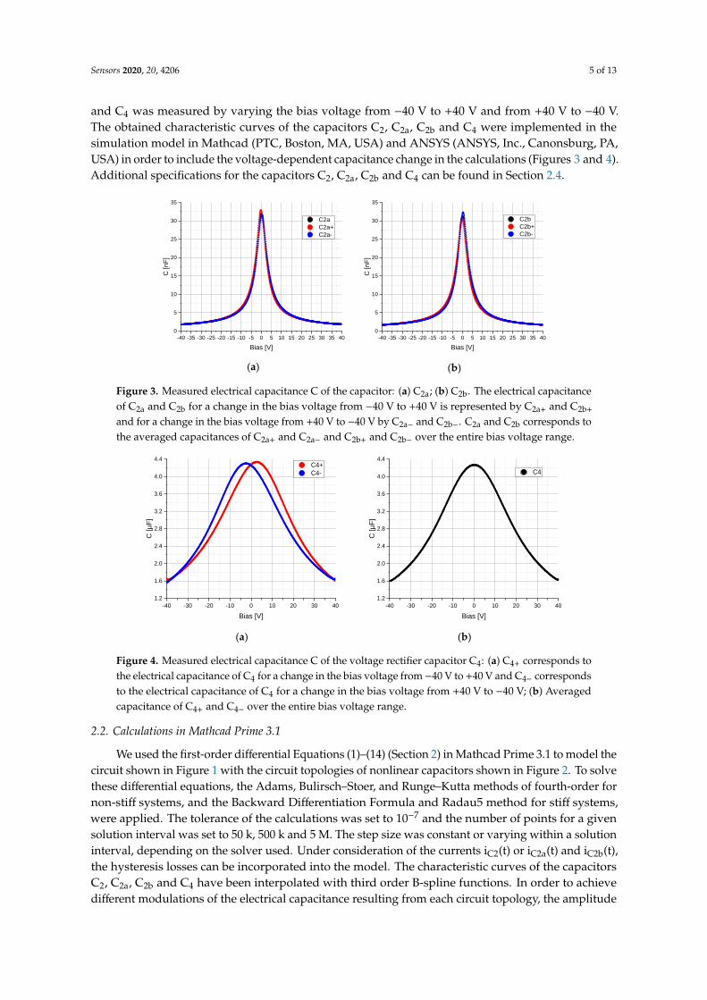
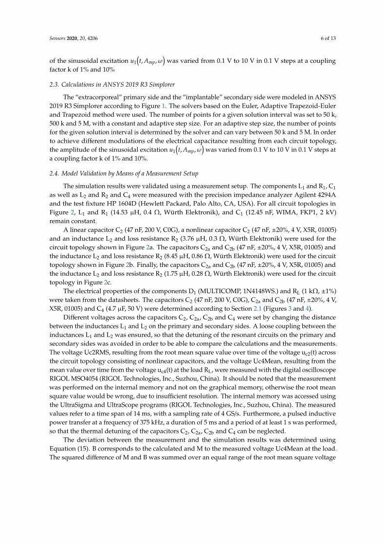
and C4 was measured by varying the bias voltage from −40 V to +40 V and from +40 V to −40 V.The obtained characteristic curves of the capacitors C2, C2a, C2b and C4 were implemented in thesimulation model in Mathcad (PTC, Boston, MA, USA) and ANSYS (ANSYS, Inc., Canonsburg, PA,USA) in order to include the voltage-dependent capacitance change in the calculations (Figures 3 and 4).Additional specifications for the capacitors C2, C2a, C2b and C4 can be found in Section 2.4.
Sensors 2020, 20, x FOR PEER REVIEW 5 of 15
in Mathcad (PTC, Boston, MA, USA) and ANSYS (ANSYS, Inc., Canonsburg, PA, USA) in order to
include the voltage-dependent capacitance change in the calculations (Figures 3 and 4). Additional
specifications for the capacitors C2, C2a, C2b and C4 can be found in Section 2.4.
-40 -35 -30 -25 -20 -15 -10 -5 0 5 10 15 20 25 30 35 40
0
5
10
15
20
25
30
35
C2a
C2a+
C2a-
C [n
F]
Bias [V] -40 -35 -30 -25 -20 -15 -10 -5 0 5 10 15 20 25 30 35 40
0
5
10
15
20
25
30
35
C2b
C2b+
C2b-
C [n
F]
Bias [V]
(a) (b)
Figure 3. Measured electrical capacitance C of the capacitor: (a) C2a; (b) C2b. The electrical capacitance
of C2a and C2b for a change in the bias voltage from −40 V to +40 V is represented by C2a+ and C2b+ and
for a change in the bias voltage from +40 V to −40 V by C2a− and C2b−. C2a and C2b corresponds to the
averaged capacitances of C2a+ and C2a− and C2b+ and C2b− over the entire bias voltage range.
-40 -30 -20 -10 0 10 20 30 40
1.2
1.6
2.0
2.4
2.8
3.2
3.6
4.0
4.4 C4+
C4-
C [µ
F]
Bias [V] -40 -30 -20 -10 0 10 20 30 40
1.2
1.6
2.0
2.4
2.8
3.2
3.6
4.0
4.4
C4
C [µ
F]
Bias [V]
(a) (b)
Figure 4. Measured electrical capacitance C of the voltage rectifier capacitor C4: (a) C4+ corresponds to
the electrical capacitance of C4 for a change in the bias voltage from −40 V to +40 V and C4− corresponds
to the electrical capacitance of C4 for a change in the bias voltage from +40 V to −40 V; (b) Averaged
capacitance of C4+ and C4− over the entire bias voltage range.
2.2. Calculations in Mathcad Prime 3.1
We used the first-order differential Equations (1)–(14) (Section 2) in Mathcad Prime 3.1 to model
the circuit shown in Figure 1 with the circuit topologies of nonlinear capacitors shown in Figure 2. To
solve these differential equations, the Adams, Bulirsch–Stoer, and Runge–Kutta methods of fourth-
order for non-stiff systems, and the Backward Differentiation Formula and Radau5 method for stiff
systems, were applied. The tolerance of the calculations was set to 10−7 and the number of points for
a given solution interval was set to 50 k, 500 k and 5 M. The step size was constant or varying within
a solution interval, depending on the solver used. Under consideration of the currents iC2(t) or iC2a(t)
and iC2b(t), the hysteresis losses can be incorporated into the model. The characteristic curves of the
capacitors C2, C2a, C2b and C4 have been interpolated with third order B-spline functions. In order to
achieve different modulations of the electrical capacitance resulting from each circuit topology, the
Figure 3. Measured electrical capacitance C of the capacitor: (a) C2a; (b) C2b. The electrical capacitanceof C2a and C2b for a change in the bias voltage from −40 V to +40 V is represented by C2a+ and C2b+
and for a change in the bias voltage from +40 V to −40 V by C2a− and C2b−. C2a and C2b corresponds tothe averaged capacitances of C2a+ and C2a− and C2b+ and C2b− over the entire bias voltage range.
Sensors 2020, 20, x FOR PEER REVIEW 5 of 15
in Mathcad (PTC, Boston, MA, USA) and ANSYS (ANSYS, Inc., Canonsburg, PA, USA) in order to
include the voltage-dependent capacitance change in the calculations (Figures 3 and 4). Additional
specifications for the capacitors C2, C2a, C2b and C4 can be found in Section 2.4.
-40 -35 -30 -25 -20 -15 -10 -5 0 5 10 15 20 25 30 35 40
0
5
10
15
20
25
30
35
C2a
C2a+
C2a-
C [n
F]
Bias [V] -40 -35 -30 -25 -20 -15 -10 -5 0 5 10 15 20 25 30 35 40
0
5
10
15
20
25
30
35
C2b
C2b+
C2b-
C [n
F]
Bias [V]
(a) (b)
Figure 3. Measured electrical capacitance C of the capacitor: (a) C2a; (b) C2b. The electrical capacitance
of C2a and C2b for a change in the bias voltage from −40 V to +40 V is represented by C2a+ and C2b+ and
for a change in the bias voltage from +40 V to −40 V by C2a− and C2b−. C2a and C2b corresponds to the
averaged capacitances of C2a+ and C2a− and C2b+ and C2b− over the entire bias voltage range.
-40 -30 -20 -10 0 10 20 30 40
1.2
1.6
2.0
2.4
2.8
3.2
3.6
4.0
4.4 C4+
C4-
C [µ
F]
Bias [V] -40 -30 -20 -10 0 10 20 30 40
1.2
1.6
2.0
2.4
2.8
3.2
3.6
4.0
4.4
C4
C [µ
F]
Bias [V]
(a) (b)
Figure 4. Measured electrical capacitance C of the voltage rectifier capacitor C4: (a) C4+ corresponds to
the electrical capacitance of C4 for a change in the bias voltage from −40 V to +40 V and C4− corresponds
to the electrical capacitance of C4 for a change in the bias voltage from +40 V to −40 V; (b) Averaged
capacitance of C4+ and C4− over the entire bias voltage range.
2.2. Calculations in Mathcad Prime 3.1
We used the first-order differential Equations (1)–(14) (Section 2) in Mathcad Prime 3.1 to model
the circuit shown in Figure 1 with the circuit topologies of nonlinear capacitors shown in Figure 2. To
solve these differential equations, the Adams, Bulirsch–Stoer, and Runge–Kutta methods of fourth-
order for non-stiff systems, and the Backward Differentiation Formula and Radau5 method for stiff
systems, were applied. The tolerance of the calculations was set to 10−7 and the number of points for
a given solution interval was set to 50 k, 500 k and 5 M. The step size was constant or varying within
a solution interval, depending on the solver used. Under consideration of the currents iC2(t) or iC2a(t)
and iC2b(t), the hysteresis losses can be incorporated into the model. The characteristic curves of the
capacitors C2, C2a, C2b and C4 have been interpolated with third order B-spline functions. In order to
achieve different modulations of the electrical capacitance resulting from each circuit topology, the
Figure 4. Measured electrical capacitance C of the voltage rectifier capacitor C4: (a) C4+ corresponds tothe electrical capacitance of C4 for a change in the bias voltage from −40 V to +40 V and C4− correspondsto the electrical capacitance of C4 for a change in the bias voltage from +40 V to −40 V; (b) Averagedcapacitance of C4+ and C4− over the entire bias voltage range.
2.2. Calculations in Mathcad Prime 3.1
We used the first-order differential Equations (1)–(14) (Section 2) in Mathcad Prime 3.1 to model thecircuit shown in Figure 1 with the circuit topologies of nonlinear capacitors shown in Figure 2. To solvethese differential equations, the Adams, Bulirsch–Stoer, and Runge–Kutta methods of fourth-order fornon-stiff systems, and the Backward Differentiation Formula and Radau5 method for stiff systems,were applied. The tolerance of the calculations was set to 10−7 and the number of points for a givensolution interval was set to 50 k, 500 k and 5 M. The step size was constant or varying within a solutioninterval, depending on the solver used. Under consideration of the currents iC2(t) or iC2a(t) and iC2b(t),the hysteresis losses can be incorporated into the model. The characteristic curves of the capacitorsC2, C2a, C2b and C4 have been interpolated with third order B-spline functions. In order to achievedifferent modulations of the electrical capacitance resulting from each circuit topology, the amplitude
Sensors 2020, 20, 4206 6 of 13
of the sinusoidal excitation u1(t, Amp,ω
)was varied from 0.1 V to 10 V in 0.1 V steps at a coupling
factor k of 1% and 10%
2.3. Calculations in ANSYS 2019 R3 Simplorer
The “extracorporeal” primary side and the “implantable” secondary side were modeled in ANSYS2019 R3 Simplorer according to Figure 1. The solvers based on the Euler, Adaptive Trapezoid-Eulerand Trapezoid method were used. The number of points for a given solution interval was set to 50 k,500 k and 5 M, with a constant and adaptive step size. For an adaptive step size, the number of pointsfor the given solution interval is determined by the solver and can vary between 50 k and 5 M. In orderto achieve different modulations of the electrical capacitance resulting from each circuit topology,the amplitude of the sinusoidal excitation u1
(t, Amp,ω
)was varied from 0.1 V to 10 V in 0.1 V steps at
a coupling factor k of 1% and 10%.
2.4. Model Validation by Means of a Measurement Setup
The simulation results were validated using a measurement setup. The components L1 and R1, C1
as well as L2 and R2 and C4 were measured with the precision impedance analyzer Agilent 4294Aand the test fixture HP 1604D (Hewlett Packard, Palo Alto, CA, USA). For all circuit topologies inFigure 2, L1 and R1 (14.53 µH, 0.4 Ω, Würth Elektronik), and C1 (12.45 nF, WIMA, FKP1, 2 kV)remain constant.
A linear capacitor C2 (47 nF, 200 V, C0G), a nonlinear capacitor C2 (47 nF, ±20%, 4 V, X5R, 01005)and an inductance L2 and loss resistance R2 (3.76 µH, 0.3 Ω, Würth Elektronik) were used for thecircuit topology shown in Figure 2a. The capacitors C2a and C2b (47 nF, ±20%, 4 V, X5R, 01005) andthe inductance L2 and loss resistance R2 (8.45 µH, 0.86 Ω, Würth Elektronik) were used for the circuittopology shown in Figure 2b. Finally, the capacitors C2a and C2b (47 nF, ±20%, 4 V, X5R, 01005) andthe inductance L2 and loss resistance R2 (1.75 µH, 0.28 Ω, Würth Elektronik) were used for the circuittopology in Figure 2c.
The electrical properties of the components D1 (MULTICOMP, 1N4148WS.) and RL (1 kΩ, ±1%)were taken from the datasheets. The capacitors C2 (47 nF, 200 V, C0G), C2a and C2b (47 nF, ±20%, 4 V,X5R, 01005) and C4 (4.7 µF, 50 V) were determined according to Section 2.1 (Figures 3 and 4).
Different voltages across the capacitors C2, C2a, C2b and C4 were set by changing the distancebetween the inductances L1 and L2 on the primary and secondary sides. A loose coupling between theinductances L1 and L2 was ensured, so that the detuning of the resonant circuits on the primary andsecondary sides was avoided in order to be able to compare the calculations and the measurements.The voltage Uc2RMS, resulting from the root mean square value over time of the voltage uc2(t) acrossthe circuit topology consisting of nonlinear capacitors, and the voltage Uc4Mean, resulting from themean value over time from the voltage uc4(t) at the load RL, were measured with the digital oscilloscopeRIGOL MSO4054 (RIGOL Technologies, Inc., Suzhou, China). It should be noted that the measurementwas performed on the internal memory and not on the graphical memory, otherwise the root meansquare value would be wrong, due to insufficient resolution. The internal memory was accessed usingthe UltraSigma and UltraScope programs (RIGOL Technologies, Inc., Suzhou, China). The measuredvalues refer to a time span of 14 ms, with a sampling rate of 4 GS/s. Furthermore, a pulsed inductivepower transfer at a frequency of 375 kHz, a duration of 5 ms and a period of at least 1 s was performed,so that the thermal detuning of the capacitors C2, C2a, C2b and C4 can be neglected.
The deviation between the measurement and the simulation results was determined usingEquation (15). B corresponds to the calculated and M to the measured voltage Uc4Mean at the load.The squared difference of M and B was summed over an equal range of the root mean square voltage
Sensors 2020, 20, 4206 7 of 13
Uc2RMS from 0.7 V to 21 V with a step size of 10 mV and subsequently divided by the number ofsteps, N. For this calculation, M and B were piecewise linearly interpolated.
S =
√1N
∑(M− B)2 (15)
3. Results and Discussion
First, we show the results for the circuit in Figure 1 with the circuit topology in Figure 2a havinga linear capacitor C2 (47 nF, 200 V, C0G) and C4 (4.7 µF, 50 V). The capacitors C2 and C4 were defined asconstant at 48 nF and 4.56 µF. The deviation S between the calculations with ANSYS/Mathcad and themeasurements is shown in Table 1.
Table 1. Deviations between the measured and calculated voltage Uc4Mean in a range of Uc2RMSfrom 0.7 V to 21 V at a coupling factor k of 1%.
Method 50 k Points 500 k Points 5 M Points
Adams 0.5 V 0.5 V 0.5 VBulirsch–Stoer 0.3 V 0.3 V 0.3 VRunge–Kutta 1 0.5 V 0.5 V 0.5 VRunge–Kutta 2 0.3 V 0.3 V 0.3 V
BDF 4 0.5 V 0.5 V 0.5 VRadau5 0.5 V 0.5 V 0.5 VEuler 1 15.5 V 14.8 V 0.5 V
Trapezoid 1 0.5 V 0.6 V 0.6 VATE 1,3 10.7 V 0.6 V 0.6 VEuler 2 15.5 V
Trapezoid 2 0.6 VATE 2,3 0.5 V
1 With constant step size; 2 With variable step size; 3 Adaptive Trapezoid-Euler; 4 Backward Differentiation Formula.
All selected calculation methods in Mathcad, regardless of the applied resolution, show a smalldeviation. A high consistency between calculations and measurements can also be achieved inANSYS, except for the Euler method with constant step size and a resolution of 50 k and 500 kpoints and an adaptive step size, and the Adaptive Trapezoid-Euler method with constant step sizeand a resolution of 50 k points. Table 1 shows that in case of a linear capacitor C2 and C4, most calculationmethods in ANSYS and all calculation methods in Mathcad lead to a high consistency betweencalculations and measurements. As an additional result, the memory consumption and computing timeof the calculation methods used in Table 1 are shown in Tables 2 and 3, respectively. The calculationswere performed on a workstation HP Z250 (L8T12AV, Intel Xeon E3-1280 v5 (8M Cache, 3.70 GHz),32 GB DDR4, 256 GB SSD, Windows 10 Pro 64-bit).
Table 2 shows that the calculations with Mathcad generally require less memory than with ANSYS,because the results obtained with Mathcad can be stored in binary format. For calculations with Mathcadand ANSYS with equal resolution of 50 k, 500 k and 5 M points and with constant step size, the memoryconsumption for calculations with ANSYS is about 5 times higher than with Mathcad. The memoryconsumption for the Euler and Adaptive Trapezoid-Euler methods (ANSYS) with an adaptive step sizeis about the same as for the calculation methods used in Mathcad at a resolution of 500 k points. On theother hand, the memory consumption for the Trapezoid method with an adaptive step size is about1.5 times higher than with the calculations in Mathcad with a resolution of 5 M points. In terms ofconsistency and memory consumption, the Adams, Bulirsch–Stoer, Backward Differentiation Formula,Radau5 and the fourth-order Runge–Kutta method with constant and adaptive step size and a resolutionof 50 k points (Mathcad) and the Trapezoid method with constant step size and a resolution of 50 kpoints (ANSYS) are most suitable.
Sensors 2020, 20, 4206 8 of 13
Table 2. Memory consumption of the selected calculation methods in Mathcad and ANSYS summedup over 100 independent runs.
Method 50 k Points 500 k Points 5 M Points
Adams 0.23 GB 2.23 GB 22.3 GBBulirsch–Stoer 0.23 GB 2.23 GB 22.3 GBRunge–Kutta 1 0.23 GB 2.23 GB 22.3 GBRunge–Kutta 2 0.23 GB 2.23 GB 22.3 GB
BDF 4 0.23 GB 2.23 GB 22.3 GBRadau5 0.23 GB 2.23 GB 22.3 GBEuler 1 1.18 GB 11.7 GB 118 GB
Trapezoid 1 1.18 GB 11.7 GB 117 GBATE 1,3 1.18 GB 11.7 GB 117 GBEuler 2 2.84 GB
Trapezoid 2 34.9 GBATE 2,3 2.33 GB
1 With constant step size; 2 With variable step size; 3 Adaptive Trapezoid-Euler; 4 Backward-Differentiation-Formula.
Table 3. Computing time (hh:mm:ss) of the selected calculation methods in Mathcad summed up over80 independent runs.
Method 50 k Points 500 k Points 5 M Points
Adams 00:03:17 00:03:49 00:10:03Bulirsch–Stoer 00:16:17 01:12:57 08:56:55Runge–Kutta 1 00:01:48 00:15:41 02:42:50Runge–Kutta 2 00:07:58 00:42:35 06:39:06
BDF 4 00:12:33 00:12:48 00:19:13Radau5 00:07:42 00:08:33 00:13:11Euler 1 00:01:51 00:06:29 00:44:27
Trapezoid 1 00:01:45 00:06:17 00:52:25ATE 1,3 00:04:43 00:14:30 00:43:16Euler 2 00:02:49
Trapezoid 2 00:21:13ATE 2,3 00:02:04
1 With constant step size; 2 With variable step size; 3 Adaptive Trapezoid-Euler; 4 Backward-Differentiation-Formula.
Table 3 shows that the calculations with a resolution of 50 k points show the lowest computingtime. It should also be noted that the Bulirsch–Stoer method with a resolution of 50 k, 500 kand 5 M points shows the highest computing time. In addition, the computing time with theAdams, Backward Differentiation Formula and Radau5 method changes only slightly at the differentresolutions. In terms of consistency, memory consumption and computing time, the Adams, Radau5and fourth-order Runge–Kutta method with a constant and adaptive step size and a resolution of 50 kpoints are most suitable in Mathcad and the Trapezoid method with a constant step size and a resolutionof 50 k points is most suitable in ANSYS.
However, despite the small deviation, discrepancies in amplitude and time constants between thecalculated and measured time-related voltage Uc4 were observed (Figure 5a). The same discrepancieshave been observed in the previously published conference paper [19], although it was not clearwhether they were due to the modeling of the two serially connected nonlinear capacitors, C2a andC2b, or to another cause. Since these discrepancies occur in the case of both, a linear capacitor C2 andtwo serially connected nonlinear capacitors, C2a and C2b, they cannot be assigned to the modeling ofthe nonlinear capacitors.
To find the root cause, the impact of the coupling factor k on the above-mentioned discrepancieswas investigated. For this purpose, the calculations were performed with the circuit shown in Figure 1having a linear capacitor C2 (Figure 2a) and C4. The coupling factor was varied from 1% to 10% in 1%steps and the amplitude of the sinusoidal voltage source was adjusted so that the voltage Uc2RMS was

Sensors 2020, 20, 4206 9 of 13
equal to 2.123 V. Figure 5 shows that an increasing coupling factor directly impacts the amplitude andtime constant of the voltage Uc4. By changing the coupling factor between 1% and 4% (Figure 5a),the amplitude and time constant of voltage Uc4 change significantly. For coupling factors above4%, the impact of the coupling factor on the amplitude and time constant becomes less significant(Figure 5b,c). At a coupling factor between 7% and 10%, the consistency between the calculatedand measured time-related voltage curves Uc4 is highest (Figure 5c). Consequently, it should beensured that the coupling factor is sufficiently high to achieve more accurate results even in the case ofloose coupling.Sensors 2020, 20, x FOR PEER REVIEW 10 of 15
(a) (b) (c)
Figure 5. Representation of the measured (black) and calculated voltage Uc4 (Mathcad) over time t.
Table 2. RMS was set to 2.123 V and the coupling factor k between the two inductances, L1 and L2,
was set to: (a) 1% (red), 2% (green), 3% (blue), 4% (pink); (b) 5% (red), 6% (green), 7% (blue); (c) 8%
(red), 9% (green), 10% (blue).
Finally, the impact of the nonlinear properties of the capacitor C4 on the model consistency was
determined. The calculations were performed with the circuit in Figure 1 having a linear capacitor C2
(Figure 2a), a nonlinear capacitor C4 (Figure 4) and a coupling factor of 10%. According to Figure 6,
the nonlinearity of the voltage rectifier capacitor C4 has no significant impact on the consistency of
the model.
Figure 6. Representation of the measured (black) and calculated voltage (Mathcad) over time t. The
voltage Uc2RMS was set to 2.123 V and the coupling factor, k, between the two inductances, L1 and
L2, was set to 10%. Linear capacitor C4 (red), nonlinear capacitor C4 (green).
Based on these results, the calculations from Table 1 were repeated with a coupling factor k of
10%. Table 4 shows that increasing the coupling factor from 1% to 10% reduces the overall deviation,
except for the Euler method with a resolution of 50 k points and a constant and adaptive step size.
The reduction in deviation is especially noticeable in the Euler and Adaptive Trapezoid-Euler
method. The deviation was reduced from 14.8 V to 0.3 V for the Euler method with constant step size
and a resolution of 500 k points, and from 10.7 V to 0.3 V for the Adaptive Trapezoid-Euler method
with constant step size and a resolution of 50 k points.
0 1 2 3 4 5 6 7 8 9 10 11 12
0.0
0.5
1.0
1.5
2.0
2.5
3.0
Uc4
[V
]
t [ms]
Uc2RMS = 2.123 V
0 1 2 3 4 5 6 7 8 9 10 11 12
0.0
0.5
1.0
1.5
2.0
2.5
3.0
Uc4
[V
]
t [ms]
Uc2RMS = 2.123 V
0 1 2 3 4 5 6 7 8 9 10 11 12
0.0
0.5
1.0
1.5
2.0
2.5
3.0
Uc4
[V
]
t [ms]
Uc2RMS = 2.123 V
0 1 2 3 4 5 6 7 8 9 10 11 12
0.0
0.5
1.0
1.5
2.0
2.5
3.0
Uc4
[V
]
t [ms]
Uc2RMS = 2.123 V
Figure 5. Representation of the measured (black) and calculated voltage Uc4 (Mathcad) over time t.Table 2. RMS was set to 2.123 V and the coupling factor k between the two inductances, L1 and L2, wasset to: (a) 1% (red), 2% (green), 3% (blue), 4% (pink); (b) 5% (red), 6% (green), 7% (blue); (c) 8% (red),9% (green), 10% (blue).
Finally, the impact of the nonlinear properties of the capacitor C4 on the model consistency wasdetermined. The calculations were performed with the circuit in Figure 1 having a linear capacitor C2
(Figure 2a), a nonlinear capacitor C4 (Figure 4) and a coupling factor of 10%. According to Figure 6,the nonlinearity of the voltage rectifier capacitor C4 has no significant impact on the consistency ofthe model.
Based on these results, the calculations from Table 1 were repeated with a coupling factor k of10%. Table 4 shows that increasing the coupling factor from 1% to 10% reduces the overall deviation,except for the Euler method with a resolution of 50 k points and a constant and adaptive stepsize. The reduction in deviation is especially noticeable in the Euler and Adaptive Trapezoid-Eulermethod. The deviation was reduced from 14.8 V to 0.3 V for the Euler method with constant step sizeand a resolution of 500 k points, and from 10.7 V to 0.3 V for the Adaptive Trapezoid-Euler methodwith constant step size and a resolution of 50 k points.
Sensors 2020, 20, x FOR PEER REVIEW 10 of 15
(a) (b) (c)
Figure 5. Representation of the measured (black) and calculated voltage Uc4 (Mathcad) over time t.
Table 2. RMS was set to 2.123 V and the coupling factor k between the two inductances, L1 and L2,
was set to: (a) 1% (red), 2% (green), 3% (blue), 4% (pink); (b) 5% (red), 6% (green), 7% (blue); (c) 8%
(red), 9% (green), 10% (blue).
Finally, the impact of the nonlinear properties of the capacitor C4 on the model consistency was
determined. The calculations were performed with the circuit in Figure 1 having a linear capacitor C2
(Figure 2a), a nonlinear capacitor C4 (Figure 4) and a coupling factor of 10%. According to Figure 6,
the nonlinearity of the voltage rectifier capacitor C4 has no significant impact on the consistency of
the model.
Figure 6. Representation of the measured (black) and calculated voltage (Mathcad) over time t. The
voltage Uc2RMS was set to 2.123 V and the coupling factor, k, between the two inductances, L1 and
L2, was set to 10%. Linear capacitor C4 (red), nonlinear capacitor C4 (green).
Based on these results, the calculations from Table 1 were repeated with a coupling factor k of
10%. Table 4 shows that increasing the coupling factor from 1% to 10% reduces the overall deviation,
except for the Euler method with a resolution of 50 k points and a constant and adaptive step size.
The reduction in deviation is especially noticeable in the Euler and Adaptive Trapezoid-Euler
method. The deviation was reduced from 14.8 V to 0.3 V for the Euler method with constant step size
and a resolution of 500 k points, and from 10.7 V to 0.3 V for the Adaptive Trapezoid-Euler method
with constant step size and a resolution of 50 k points.
0 1 2 3 4 5 6 7 8 9 10 11 12
0.0
0.5
1.0
1.5
2.0
2.5
3.0
Uc4
[V
]
t [ms]
Uc2RMS = 2.123 V
0 1 2 3 4 5 6 7 8 9 10 11 12
0.0
0.5
1.0
1.5
2.0
2.5
3.0
Uc4
[V
]
t [ms]
Uc2RMS = 2.123 V
0 1 2 3 4 5 6 7 8 9 10 11 12
0.0
0.5
1.0
1.5
2.0
2.5
3.0
Uc4
[V
]
t [ms]
Uc2RMS = 2.123 V
0 1 2 3 4 5 6 7 8 9 10 11 12
0.0
0.5
1.0
1.5
2.0
2.5
3.0
Uc4
[V
]
t [ms]
Uc2RMS = 2.123 V
Figure 6. Representation of the measured (black) and calculated voltage (Mathcad) over time t.The voltage Uc2RMS was set to 2.123 V and the coupling factor, k, between the two inductances,L1 and L2, was set to 10%. Linear capacitor C4 (red), nonlinear capacitor C4 (green).

Sensors 2020, 20, 4206 10 of 13
Table 4. Deviations between the measured and calculated voltage Uc4Mean in a range of Uc2RMSfrom 0.7 V to 21 V at a coupling factor k of 10%.
Method 50 k Points 500 k Points 5 M Points
Adams 0.3 V 0.3 V 0.3 VBulirsch–Stoer 0.3 V 0.3 V 0.3 VRunge–Kutta 1 0.4 V 0.3 V 0.3 VRunge–Kutta 2 0.3 V 0.3 V 0.3 V
BDF 4 0.3 V 0.3 V 0.3 VRadau5 0.3 V 0.3 V 0.3 VEuler 1 15.5 V 0.3 V 0.4 V
Trapezoid 1 0.4 V 0.4 V 0.4 VATE 1,3 0.3 V 0.4 V 0.4 VEuler 2 15.1 V
Trapezoid 2 0.4 VATE 2,3 0.4 V
1 With constant step size; 2 With variable step size; 3 Adaptive Trapezoid-Euler; 4 Backward Differentiation Formula.
The measurements and calculations in Figure 7 can be split into two parts. A part in which therelationship between Uc4Mean and Uc2RMS is linear and a part in which the nonlinear properties ofthe circuit topologies shown in Figure 2 are effective. Within the linear range, the consistency betweencalculations and measurements is high. However, Figure 7 shows that the threshold values to bereached by Uc2RMS for triggering the nonlinear behavior on Uc4Mean are lower in the calculationsthan in the measurements. The same observation was also made in the previous conference paper [19].The impact of the hysteresis losses on the calculations is particularly noticeable in the circuit topologyconsisting of two serially connected nonlinear capacitors, C2a and C2b (Figure 7b). The value of Uc2RMSat which the voltage Uc4Mean increases changes from about 23 V to 20 V due to the hysteresis losses.The same behavior can also be observed with a nonlinear capacitor, C2, and two nonlinear capacitors,C2a and C2b, connected in parallel (Figure 7a,c), in a range of Uc2RMS between about 6 V and 9 V.An interesting point in Figure 7 is that depending on the circuit topology used, an approximatelyconstant range of Uc4Mean is achieved within a specific range of Uc2RMS. The range of Uc2RMS inwhich Uc4Mean is approximately constant and the slope of Uc4Mean within this range are defined bythe circuit topology of nonlinear capacitors.Sensors 2020, 20, x FOR PEER REVIEW 12 of 15
(a) (b) (c)
Figure 7. Representation of the measured (blue) and calculated voltage Uc4Mean with hysteresis
losses (red) and without hysteresis losses (black) versus the voltage Uc2RMS. The calculations were
performed for a circuit topology consisting of: (a) one nonlinear capacitor, C2 (see Figure 2a); (b) two
serially connected nonlinear capacitors, C2a and C2b, (see Figure 2b); (c) two nonlinear capacitors, C2a
and C2b, connected in parallel (see Figure 2c). Furthermore, the Adams method was used with a
resolution of 50 k points and a coupling factor k of 10%.
4. Conclusions
This paper describes the optimization steps for modeling the nonlinear properties of ferroelectric
materials in ceramic capacitors in terms of consistency, memory consumption and computing time.
It turned out that the coupling factor k directly impacts the consistency between simulation and
measurement. Particular attention should be paid to ensure a sufficiently high coupling factor k even
in the case of loose coupling. A coupling factor between 7% and 10% should be adequate to properly
model the time constant of the inductive power transmission system.
In addition, it was found that the consideration of the nonlinear properties of the capacitor C4
does not significantly improve the model, but increases the computing time. Therefore, with regard
to consistency and computing time, we recommend neglecting the nonlinear properties of the
capacitor C4 for further modeling purposes.
Based on the results of the previously published conference paper, it was concluded that the
Trapezoid method with a constant step size and a resolution of 500 k points and with an adaptive
step size is most suitable in ANSYS [19]. Considering the computing time and memory consumption
in Tables 2 and 3, the Trapezoid method with a constant step size and a resolution of 500 k points
should be preferred.
A high consistency between calculations and measurements was achieved in Mathcad using the
Adams, Bulirsch–Stoer, Backward Differentiation Formula, Radau5, and fourth-order Runge–Kutta
method with an adaptive step size and a resolution of 50 k points. The calculations in Mathcad with
a resolution of 50 k points show the lowest memory consumption (Table 2). With regard to the
computing time, we recommend using the Adams method in the first place and the Backward
Differentiation Formula and Radau5 method as an alternative (Table 3).
Based on these results, a simulation model for modeling ferroelectric materials in ceramic
capacitors is now available that exhibits high consistency and efficiency in terms of computing time
and memory consumption. Nevertheless, the simulation model is limited to lower AC voltages across
the circuit topology of nonlinear capacitors. In order to expand the application of the model to higher
AC voltages, it is necessary in the next step to characterize the voltage dependence of ceramic
capacitors for large signals. Furthermore, the impact of the manufacturing tolerances of ferroelectric
capacitors on the robustness of the collective nonlinear dynamics of the proposed meaningful circuit
topology should be investigated [28].
We plan to use this simulation model in combination with various optimization algorithms to
establish a frugal circuit topology with nonlinear components for the realization of a closed-loop
0 1 2 3 4 5 6 7 8 9 10 11 12 13 14 15 16
0
2
4
6
8
10
12
14
16
18
20
22
24
26
28
30
Uc4
Me
an
[V
]
Uc2RMS [V]
0 2 4 6 8 10 12 14 16 18 20 22 24 26 28 30 32
0
5
10
15
20
25
30
35
40
45
Uc4
Me
an
[V
]
Uc2RMS [V]
0 1 2 3 4 5 6 7 8 9 10 11 12 13 14 15
0
2
4
6
8
10
12
14
16
18
20
22
24
26
28
30
32
Uc4
Me
an
[V
]
Uc2RMS [V]
Figure 7. Representation of the measured (blue) and calculated voltage Uc4Mean with hysteresislosses (red) and without hysteresis losses (black) versus the voltage Uc2RMS. The calculations wereperformed for a circuit topology consisting of: (a) one nonlinear capacitor, C2 (see Figure 2a); (b) twoserially connected nonlinear capacitors, C2a and C2b, (see Figure 2b); (c) two nonlinear capacitors,C2a and C2b, connected in parallel (see Figure 2c). Furthermore, the Adams method was used witha resolution of 50 k points and a coupling factor k of 10%.
Sensors 2020, 20, 4206 11 of 13
Despite the increase in the coupling factor k from 1% to 10% and the implementation of hysteresislosses, the calculations deviate from the measurements for higher values of Uc2RMS. A possibleexplanation would be that the measurement of the nonlinear capacitors used in this work, according toSection 2.1, is no longer valid for higher AC voltages [25–27].
4. Conclusions
This paper describes the optimization steps for modeling the nonlinear properties of ferroelectricmaterials in ceramic capacitors in terms of consistency, memory consumption and computingtime. It turned out that the coupling factor k directly impacts the consistency between simulationand measurement. Particular attention should be paid to ensure a sufficiently high coupling factork even in the case of loose coupling. A coupling factor between 7% and 10% should be adequate toproperly model the time constant of the inductive power transmission system.
In addition, it was found that the consideration of the nonlinear properties of the capacitor C4
does not significantly improve the model, but increases the computing time. Therefore, with regard toconsistency and computing time, we recommend neglecting the nonlinear properties of the capacitorC4 for further modeling purposes.
Based on the results of the previously published conference paper, it was concluded that theTrapezoid method with a constant step size and a resolution of 500 k points and with an adaptive stepsize is most suitable in ANSYS [19]. Considering the computing time and memory consumption inTables 2 and 3, the Trapezoid method with a constant step size and a resolution of 500 k points shouldbe preferred.
A high consistency between calculations and measurements was achieved in Mathcad using theAdams, Bulirsch–Stoer, Backward Differentiation Formula, Radau5, and fourth-order Runge–Kuttamethod with an adaptive step size and a resolution of 50 k points. The calculations in Mathcadwith a resolution of 50 k points show the lowest memory consumption (Table 2). With regard tothe computing time, we recommend using the Adams method in the first place and the BackwardDifferentiation Formula and Radau5 method as an alternative (Table 3).
Based on these results, a simulation model for modeling ferroelectric materials in ceramiccapacitors is now available that exhibits high consistency and efficiency in terms of computing time andmemory consumption. Nevertheless, the simulation model is limited to lower AC voltages across thecircuit topology of nonlinear capacitors. In order to expand the application of the model to higher ACvoltages, it is necessary in the next step to characterize the voltage dependence of ceramic capacitorsfor large signals. Furthermore, the impact of the manufacturing tolerances of ferroelectric capacitorson the robustness of the collective nonlinear dynamics of the proposed meaningful circuit topologyshould be investigated [28].
We plan to use this simulation model in combination with various optimization algorithms toestablish a frugal circuit topology with nonlinear components for the realization of a closed-loopcurrent control. This will increase the degree of miniaturization in electronic implants because therewill be no need to use dedicated sensors or other active electronic components. Electronic implantswith inductive power supply, such as retinal implants [1,6,7,9], cochlear implants [29,30], and thehypoglossal nerve stimulator GenioTM (Nyxoah SA, Mont-Saint-Guibert, Belgium) [31] would beparticularly suitable for this purpose.
Author Contributions: Writing—original draft, formal analysis, investigation and methodology, Y.O.; supervisionand writing—review and editing, F.R.I. All authors have read and agreed to the published version of the manuscript.
Funding: This research was funded by the German Federal Ministry of Education and Research (BMBF, fundingnumber 16SV7637K). The author is responsible for the content of this publication.
Conflicts of Interest: The authors declare no conflict of interest.

Sensors 2020, 20, 4206 12 of 13
References
1. Bloch, E.; Luo, Y.; da Cruz, L. Advances in retinal prosthesis systems. Ther. Adv. Ophthalmol. 2019,11, 2515841418817501. [CrossRef] [PubMed]
2. Stingl, K.; Bartz-Schmidt, K.U.; Besch, D.; Chee, C.K.; Cottriall, C.L.; Gekeler, F.; Groppe, M.; Jackson, T.L.;MacLaren, R.E.; Koitschev, A.; et al. Subretinal Visual Implant Alpha IMS—Clinical trial interim report.Vision Res. 2015, 111, 149–160. [CrossRef] [PubMed]
3. Mertens, A.; Raedt, R.; Gadeyne, S.; Carrette, E.; Boon, P.; Vonck, K. Recent advances in devices for vagusnerve stimulation. Expert Rev. Med. Devices 2018, 15, 527–539. [CrossRef]
4. Wray, C.M.; Thaler, E.R. Hypoglossal nerve stimulation for obstructive sleep apnea: A review of the literature.World J. Otorhinolaryngol. Head Neck Surg. 2016, 2, 230–233. [CrossRef]
5. Wolter, T.; Kieselbach, K. Cervical spinal cord stimulation: An analysis of 23 patients with long-termfollow-up. Pain Physician 2012, 15, 203–212.
6. Finn, A.P.; Grewal, D.S.; Vajzovic, L. Argus II retinal prosthesis system: A review of patient selection criteria,surgical considerations, and post-operative outcomes. Clin. Ophthalmol. 2018, 12, 1089–1097. [CrossRef]
7. Gekeler, F.; Szurman, P.; Grisanti, S.; Weiler, U.; Claus, R.; Greiner, T.-O.; Völker, M.; Kohler, K.; Zrenner, E.;Bartz-Schmidt, K.U. Compound subretinal prostheses with extra-ocular parts designed for human trials:Successful long-term implantation in pigs. Graefes Arch. Clin. Exp. Ophthalmol. 2007, 245, 230–241. [CrossRef]
8. Laube, T.; Brockmann, C.; Roessler, G.; Walter, P.; Krueger, C.; Goertz, M.; Klauke, S.; Bornfeld, N.Development of surgical techniques for implantation of a wireless intraocular epiretinal retina implant inGöttingen minipigs. Graefes Arch. Clin. Exp. Ophthalmol. 2012, 250, 51–59. [CrossRef]
9. Roessler, G.; Laube, T.; Brockmann, C.; Kirschkamp, T.; Mazinani, B.; Goertz, M.; Koch, C.; Krisch, I.;Sellhaus, B.; Trieu, H.K.; et al. Implantation and explantation of a wireless epiretinal retina implant device:Observations during the EPIRET3 prospective clinical trial. Invest. Ophthalmol. Vis. Sci. 2009, 50, 3003–3008.[CrossRef]
10. Doshi, P.K. Long-term surgical and hardware-related complications of deep brain stimulation.Stereotact. Funct. Neurosurg. 2011, 89, 89–95. [CrossRef]
11. Müller, C.; Koch, T. Control Circuit for a Base Station for Transmitting Energy to a Receiver by Means ofan Electric Resonant Circuit, Evaluation Device, Method and Computer Program. U.S. Patent ApplicationNr. 15/533,089, 10 May 2018.
12. Seo, D.; Carmena, J.M.; Rabaey, J.M.; Alon, E.; Maharbiz, M.M. Neural Dust: An Ultrasonic, Low PowerSolution for Chronic Brain-Machine Interfaces. arXiv 2013, arXiv:1307.2196.
13. Kolberg, I.; Shmilovitz, D.; Ben-Yaakov, S.S. Ceramic capacitor controlled resonant LLC converters.In Proceedings of the 2018 IEEE Applied Power Electronics Conference and Exposition (APEC), San Antonio,TX, USA, 4–8 March 2018; IEEE: Piscataway, NJ, USA, 2018; pp. 2162–2167, ISBN 978-1-5386-1180-7.
14. Borafker, S.; Drujin, M.; Ben-Yaakov, S.S. Voltage-Dependent-Capacitor Control of Wireless PowerTransfer (WPT). In Proceedings of the 2018 IEEE International Conference on the Science of ElectricalEngineering in Israel (ICSEE), Eilat, Israel, 12–14 December 2018; IEEE: Piscataway, NJ, USA, 2018; pp. 1–4,ISBN 978-1-5386-6378-3.
15. Ben-Yaakov, S.; Zeltser, I. Ceramic capacitors: Turning a deficiency into an advantage. In Proceedings of the2018 IEEE Applied Power Electronics Conference and Exposition (APEC), San Antonio, TX, USA,4–8 March 2018; IEEE: Piscataway, NJ, USA, 2018; pp. 2879–2885, ISBN 978-1-5386-1180-7.
16. Tishechkin, S.; Ben-Yaakov, S. Adaptive Capacitance Impedance Matching (ACIM) of WPT Systems byVoltage Controlled Capacitors. In Proceedings of the 2019 IEEE PELS Workshop on Emerging Technologies:Wireless Power Transfer (WoW), London, UK, 18–21 June 2019; IEEE: Piscataway, NJ, USA, 2019; pp. 396–400,ISBN 978-1-5386-7514-4.
17. Zeng, H.; Peng, F.Z. Non-linear capacitor based variable capacitor for self-tuning resonant converter inwireless power transfer. In Proceedings of the 2018 IEEE Applied Power Electronics Conference andExposition (APEC), San Antonio, TX, USA, 4–8 March 2018; IEEE: Piscataway, NJ, USA, 2018; pp. 1375–1379,ISBN 978-1-5386-1180-7.
18. Zhang, L.; Ngo, K. A Voltage-Controlled Capacitor with Wide Capacitance Range. In Proceedings of the2018 IEEE Energy Conversion Congress and Exposition (ECCE), Portland, OR, USA, 23–27 September 2018;IEEE: Piscataway, NJ, USA, 2018; pp. 7050–7054, ISBN 978-1-4799-7312-5.

Sensors 2020, 20, 4206 13 of 13
19. Olsommer, Y.; Ihmig, F.R.; Müller, C. Modeling the Nonlinear Properties of Ferroelectric Materials in CeramicCapacitors for the Implementation of Sensor Functionalities in Implantable Electronics. Proceedings 2020,42, 61. [CrossRef]
20. Brindley, G.S. Sensations produced by electrical stimulation of the occipital poles of the cerebral hemispheres,and their use in constructing visual prostheses. Ann. R. Coll. Surg. Engl. 1970, 47, 106–108. [PubMed]
21. Karny, H. Clinical and physiological aspects of the cortical visual prosthesis. Surv. Ophthalmol. 1975, 20,47–58. [CrossRef]
22. Lewis, P.M.; Rosenfeld, J.V. Electrical stimulation of the brain and the development of cortical visualprostheses: An historical perspective. Brain Res. 2016, 1630, 208–224. [CrossRef] [PubMed]
23. Mashiach, A.; Mueller, C. Head Pain Management Device Having an Antenna. U.S. Patent ApplicationNr. 14/522,248, 23 August 2016.
24. Jadli, U.; Mohd-Yasin, F.; Moghadam, H.A.; Nicholls, J.R.; Pande, P.; Dimitrijev, S. The Correct Equation forthe Current through Voltage-Dependent Capacitors. IEEE Access 2020, 8, 98038–98043. [CrossRef]
25. Institute of Electrical and Electronics Engineers; International Symposium on Electromagnetic Compatibility;EMC Europe. International Symposium on Electromagnetic Compatibility (EMC Europe), 2–6 September 2013,Brugge, Belgium; IEEE: Piscataway, NJ, USA, 2013; ISBN 978-1-4673-4980-2.
26. Cokkinides, G.J.; Becker, B. Modeling the effects of nonlinear materials in ceramic chip capacitors for use indigital and analog applications. IEEE Trans. Adv. Packag. 2000, 23, 368–374. [CrossRef]
27. Zhang, L.; Ritter, A.; Nies, C.; Dwari, S.; Guo, B.; Priya, S.; Burgos, R.; Ngo, K. Voltage-ControlledCapacitor—Feasibility Demonstration in DC–DC Converters. IEEE Trans. Power Electron. 2017, 32, 5889–5892.[CrossRef]
28. Chikhaoui, K.; Bitar, D.; Kacem, N.; Bouhaddi, N. Robustness Analysis of the Collective Nonlinear Dynamicsof a Periodic Coupled Pendulums Chain. Appl. Sci. 2017, 7, 684. [CrossRef]
29. Hochmair, I.; Nopp, P.; Jolly, C.; Schmidt, M.; Schößer, H.; Garnham, C.; Anderson, I. MED-EL CochlearImplants: State of the Art and a Glimpse Into the Future. Trends Amplif. 2006, 10, 201–219. [CrossRef]
30. Lenarz, T. Cochlear implant—state of the art. GMS Curr. Top. Otorhinolaryngol. Head Neck Surg. 2018, 16.[CrossRef]
31. Eastwood, P.R.; Barnes, M.; MacKay, S.G.; Wheatley, J.R.; Hillman, D.R.; Nguyên, X.-L.; Lewis, R.;Campbell, M.C.; Pételle, B.; Walsh, J.H.; et al. Bilateral hypoglossal nerve stimulation for treatmentof adult obstructive sleep apnoea. Eur. Respir. J. 2020, 55. [CrossRef] [PubMed]
© 2020 by the authors. Licensee MDPI, Basel, Switzerland. This article is an open accessarticle distributed under the terms and conditions of the Creative Commons Attribution(CC BY) license (http://creativecommons.org/licenses/by/4.0/).