chipkit™ mx3 board reference manual overview
TRANSCRIPT
1300 Henley Court Pullman, WA 99163
509.334.6306 www.digilentinc.com
chipKIT™ MX3 Board Reference Manual
Revised October 11, 2013 This manual applies to the chipKIT MX3 rev. B
DOC#: 502-297 Copyright Digilent, Inc. All rights reserved. Other product and company names mentioned may be trademarks of their respective owners. Page 1 of 24
Overview
chipKIT MX3 is the new name for Cerebot MX3. This board retains all functionality of the Cerebot MX3.
The chipKIT MX3 is a microcontroller development board based on the Microchip PIC32MX320F128H, a member of
the 32-bit PIC32 microcontroller family. It is compatible with Digilent's line of Pmods™, and is suitable for use with
the Microchip® MPLAB® IDE tools. The chipKIT MX3 is also compatible for use with the chipKIT MPIDE development
environment. chipKIT MPIDE is a PIC32 based system compatible with many existing Arduino™ code examples,
reference materials, and other resources.
The chipKIT MX3 is designed to be easy to use and suitable for beginners to advanced users for experimenting with
electronics and embedded control systems. It is intended to be used with either the multi-platform integrated
development environment (MPIDE, a modified Arduino IDE) or the Microchip MPLAB IDE. The kit contains
everything needed to start developing embedded applications using the MPIDE. In order to use the MPLAB IDE, an
additional programming/debugging device, such as a Microchip PICkit™3 is required.
The chipKIT MX3 provides 42 I/O pins that support a number of peripheral functions, such as UART, SPI, and I2C
ports, as well as five pulse width modulated outputs and five external interrupt inputs. Eleven of the I/O pins can
be used as analog inputs in addition to their use as digital inputs and outputs.
The chipKIT MX3 can be powered via USB, an external power supply that may be either an AC-DC power adapter,
or batteries.
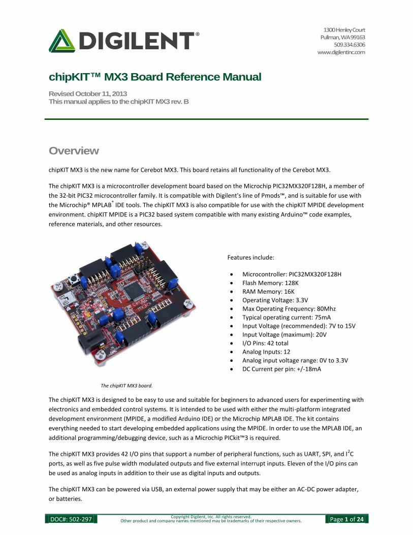
The chipKIT MX3 board.
Features include:
Microcontroller: PIC32MX320F128H
Flash Memory: 128K
RAM Memory: 16K
Operating Voltage: 3.3V
Max Operating Frequency: 80Mhz
Typical operating current: 75mA
Input Voltage (recommended): 7V to 15V
Input Voltage (maximum): 20V
I/O Pins: 42 total
Analog Inputs: 12
Analog input voltage range: 0V to 3.3V
DC Current per pin: +/-18mA

chipKIT™ MX3 Board Reference Manual
Copyright Digilent, Inc. All rights reserved. Other product and company names mentioned may be trademarks of their respective owners. Page 2 of 24
1 Programming Tools
The chipKIT MX3 is designed to be used with either the multi-platform IDE (MPIDE), the development software
environment used with the chipKIT™ system, or as a more traditional microcontroller development platform using
the Microchip MPLAB® IDE and development tools. The chipKIT MX3 if fully compatible with Microchip
development tools that support the PIC32 family of microcontrollers.
The chipKIT MX3 is immediately useable with the MPIDE. Additional hardware is required to use the Microchip
MPLAB tools.
1.1 Using the chipKIT MX3 with the MPIDE
chipKIT and the MPIDE is a PIC32 based hardware and software system compatible with many existing Arduino
code examples, reference materials, and other resources. The MPIDE development platform was produced by
modifying the Arduino IDE and is fully backward compatible with the Arduino IDE. The chipKIT MX3 board is
designed to be fully compatible with the MPIDE system, version 20111209 or later.
The MPIDE uses a serial communications port to communicate with a boot loader running in the target board. The
serial port on the MX3 board is implemented using an FTDI FT232R USB serial converter. Before attempting to use
the MPIDE to communicate with the MX3, the appropriate USB device driver must be installed.
The chipKIT MX3 board uses a standard mini-USB connector for connection to a USB port on the PC. Use a
standard USB-A to mini-B cable (not provided) to connect the board to an available USB port on the PC.
In the MPIDE, use the "Tools.Board" command to select the chipKIT MX3 from the list of available boards. Use the
"Tools.Serial Port" command to choose the appropriate serial port from the list of available serial ports on the PC.
When the MPIDE needs to communicate with the MX3 board, the board is reset and starts running the boot
loader. The MPIDE then establishes communications with the boot loader and downloads the program to the
board.
When the MPIDE opens the serial communications connection on the PC, the DTR pin on the FT232R chip is driven
low. This pin is coupled through a capacitor to the MCLR pin on the PIC32 microcontroller. Driving the MCLR line
low resets the microcontroller, restarting execution with the boot loader.

chipKIT™ MX3 Board Reference Manual
Copyright Digilent, Inc. All rights reserved. Other product and company names mentioned may be trademarks of their respective owners. Page 3 of 24
Once the MPIDE has established communication with the boot loader, it transfers the user's program to the boot
loader, which programs it into the flash memory in the Microcontroller.
The automatic reset action when the serial communications connection is opened can be disabled. To disable this
operation, remove the shorting block from jumper JP1. It is also possible that it will interfere with the operation of
the MPLAB IDE and a Microchip hardware programmer/debugger. In this case, the shorting block should also be
removed from JP1. The shorting block is reinstalled on JP1 to restore operation with the MPIDE.
Two red LEDs (LD1 and LD2) will blink when data is being sent or received between the chipKIT MX3 and the PC
over the serial connection.
The header connector J3 provides access to the other serial handshaking signals provided by the FT232R.
Connector J3 is not loaded at the factory but can be installed by the user to access these signals.
1.2 Using the chipKIT MX3 with Microchip Development Tools
In addition to being used with the MPIDE, the chipKIT MX3 can be used as a more traditional microcontroller development board using Microchip Development Tools. The Microchip MPLAB
IDE or the MPLAB X IDE can be used to program and debug code running on the chipKIT MX3
board. These programs can be downloaded from the Microchip website. These software suites include a free evaluation copy of the Microchip C32 compiler for use with the PIC32 microcontroller family. When creating a new project, use the "Configure.Select Device…" menu to specify the PIC32 device being used.
Ensure that the device is set to PIC32MX320F128H.
Programming and debugging a program on the chipKIT MX3 using the MPLAB IDE requires the use of external
programming hardware. Typically, this will be a Microchip PICkit3, but can be any other tool that supports the
same connection interface as the PICkit3 and supports the PIC32MX3XX processor family.
Connector JP3 on the left side of the board is used to connect to the Microchip hardware development tool. This connector is not loaded at the factory, but can be installed by the user if desired. The holes for JP3 are staggered so that a standard, 100mil spaced, 6-pin header can be press fit to the board without the need to solder it in place. The connector at JP3 can be soldered in place if desired for a more reliable permanent connection. Typically, a right angle male connector will be used in JP3 so that a PICkit3 can be attached coplanar with the chipKIT MX3 board. If the connector is loaded from the top, the PICkit3 will be upright (button and LEDs visible). Alternatively, the connector can be loaded from the bottom. In this case, the PICkit3 will be upside down. If JP3 is loaded from the top, the PICkit3 will interfere with the USB connector and the external power connector. A short six-wire cable can be used between the PICkit3 and the chipKIT MX3. If JP3 is loaded from the bottom, the PICkit3 will not interfere with the USB and external power connectors. Digilent has a kit available (PICkit3 Programming Cable Kit) that includes all necessary connectors and the cable for connecting a PICkit3 to the chipKIT MX3. The MCLR pin on the PIC32 microcontroller is used by the hardware programming/debugging interface to reset the
processor. This same pin is used by the USB serial converter to reset the processor when using the MPIDE. It is
possible that the reset function from the USB serial interface can interfere with correct operation of the Microchip
programming and debugging tools. If this happens, jumper JP1 can be used to disconnect the USB serial converter
reset circuit. Remove the shorting block from JP1 to disable the reset circuit. If the shorting block has been
removed, it is necessary to reinstall it on JP1 in order to use the chipKIT MX3 board with the MPIDE again.

chipKIT™ MX3 Board Reference Manual
Copyright Digilent, Inc. All rights reserved. Other product and company names mentioned may be trademarks of their respective owners. Page 4 of 24
Using the Microchip development tools to program the chipKIT MX3 will erase the boot loader. To use the board with the MPIDE again, it is necessary to program the boot loader back onto the board. The programming file for the boot loader programmed into the board by Digilent at the factory is available for download from the product page for the chipKIT MX3 on the Digilent web site. Additionally, the boot loader source code is available in the chipKIT project repository at www.github.com/chipKIT32/pic32-Arduino-Bootloader. To reprogram the boot loader using MPLAB, perform the following steps:
Use the "Configure.Select Device …" menu to select the PIC32MX320F128H
Use the "Programmer.Select Programmer" menu to select the "PICkit3" or other hardware programming tool being used.
Use the "File Import…" dialog box to navigate to and select the boot loader programming downloaded from the Digilent web site. The file name will be something like: chipKIT_Bootloader_MX3.hex
Use the "Programmer.Program" command to program all memories on the device.
1.3 Additional Reference Documentation
For additional information about the chipKIT MX3 board and the use and operation of the PIC32MX320F128H
microcontroller, refer to the following documents in addition to this reference manual.
The chipKIT MX3 Schematic, available on the chipKIT MX3 product page on the Digilent web site:
www.digilentinc.com
The PIC32MX3XX/4XX Family Data Sheet and the PIC32MX Family Reference Manual available from the Microchip
web site: www.microchip.com
Additional reference material for the MPIDE system is included in the MPIDE software download, and on-line in
the chipKIT wiki. Help with questions and problems using the board with the MPIDE software can also be obtained
in the chipKIT forums:
www.chipKIT.net/install (software download)
www.chipKIT.net
www.chipKIT.org/forum
2 Power Supply
The chipKIT MX3 is designed to be powered either from USB or from an external power supply. There is an
automatic switchover circuit that causes the external supply to be used if both supplies are present.
The power supply section uses two voltage regulators. The first regulates the external voltage to 5V to power the
VCC5V0 bus. The second regulates the VCC5V0 bus to 3.3V to provide power to the VCC3V3 bus that powers the
PIC32 microcontroller.
The 5V voltage regulator, IC2, is normally an NCP1117. The board is designed to be able to also use an LM1117, but
the NCP1117 is the part normally used. The NCP1117 is rated for an output current of 1A (the LM1117 is rated for
800mA). The dropout voltage of the NCP1117 is a maximum of 1.2V at the rated output current (1.3V for the
LM1117). There is a reverse polarity protection diode in the external power supply circuit. Considering the diode
drop plus the forward drop across the regulator, the minimum input voltage to the regulator should be 7V to

chipKIT™ MX3 Board Reference Manual
Copyright Digilent, Inc. All rights reserved. Other product and company names mentioned may be trademarks of their respective owners. Page 5 of 24
produce a reliable 5V output. The absolute maximum input voltage of both the NCP1117 and the LM1117 is 20V.
The recommended maximum operating voltage is 15V. For input voltages above 9V, the regulator will get
extremely hot when drawing high currents. Both the NCP1117 and the LM1117 have output short circuit
protection and internal thermal protection and will shut down automatically to prevent damage.
The 3.3V regulator, IC3, is a Microchip MCP1725. This regulator is rated for a maximum output current of 500mA.
The absolute maximum input voltage for the MCP1725 is 6V. This regulator has internal short circuit protection
and thermal protection. It will get noticeably warm when the current consumed by the VCC3V3 bus is close to the
500mA maximum.
The 5V power bus, VCC5V0 can be powered from one of three sources: 1) The USB5V0 bus when the board is
operating under USB power; 2) The output of the on-board 5V regulator when operating from an external 7V–15V
supply; or 3) Directly from the external supply when operating from a regulated 5V external supply and jumper JP2
is in the BYP position.
Switchover from USB power to external power is done automatically and the external supply will be used if both
are present.
Jumper JP2 is used to route the external power supply voltage through the on-board 5V regulator or directly to the
VCC5V0 bus, bypassing the on-board 5V regulator. Normally, JP2 should be in the REG position. This routes the
external supply through the 5V regulator. Operation from an externally regulated 5V supply is accomplished by
placing the jumper in the BYP position.
The forward drop across the MCP1725 is typically 210mV (350mV max) at 500mA output. With JP2 in the BYP
position, this will allow correct operation of the 3.3V power supply from an input voltage down to 3.5V. This allows
powering the board from batteries and other lower voltage power sources. In this case, the VCC5V0 power bus will
not be powered at 5V.
NOTE: It is extremely important to observe the MCP1725 maximum input voltage rating of 6V when JP2 is in the
BYP position. Applying more than 6V to the external power input with the jumper in the BYP position can damage
the 3.3V regulator and possibly the PIC32 microcontroller as well.
The PIC32 microcontroller is rated to use a maximum of 75mA of current when operating at 80 MHz. This allows up
to 425mA from the VCC3V3 bus and up to 925mA from the VCC5V0 bus to power external devices. The combined
power used by the VCC5V0 bus and the VCC3V3 bus should not exceed 925mA.
The chipKIT MX3 can provide power to any peripheral modules attached to the Pmod connectors, JA-JE, and to I2C
devices connected to the I2C daisy chain connector, J2. Each Pmod connector provides power pins that can be
powered from either the switched main power bus, VCC5V0, or the regulated voltage, VCC3V3, by setting the
voltage jumper block to the desired position.
The I2C power connector only provides 3.3V from the VCC3V3 bus.
It is also possible to power the chipKIT MX3 from any one of the Pmod connectors or the I2C connector. When
powering the board from a Pmod connector with the power select jumper in the 5V0 position, a voltage applied at
the Pmod connector will power the VCC5V0 bus and be regulated to 3.3V for the VCC3V3 bus. When powering the
board from the I2C connector or a Pmod connector with the power select jumper in the 3V3 position, only the
VCC3V3 bus will be powered and the VCC5V0 bus will not be powered.
chipKIT™ MX3 Board Reference Manual
Copyright Digilent, Inc. All rights reserved. Other product and company names mentioned may be trademarks of their respective owners. Page 6 of 24
2.1 RESET
A reset button is at the upper left corner of the board. Pressing this button will reset the PIC32 microcontroller.
3 Pmod™ Connectors
The chipKIT MX3 has five connectors for connecting Digilent Pmod peripheral modules. The Pmod connectors,
labeled JA–JF, are 2x8 right-angle, female pin header connectors. Each connector has an associated power select
jumper block labeled JPA–JPF.
Digilent Pmods are a line of small peripheral modules that provide various kinds of I/O interfaces. The Pmod
product line includes such things as button, switch and LED modules, connector modules, LCD displays, high
current output drivers, and many others.
There are two styles of Pmod connector: six-pin and twelve-pin. Both connectors use standard pin headers with
100mil spaced pins. The six-pin connectors have the pins in a 1x6 configuration, while the twelve-pin connectors
use a 2x6 configuration. All of the Pmod connectors on the chipKIT MX3 are twelve pin connectors.
The six-pin connectors provide four I/O signals, ground and a switchable power connection. The twelve-pin
connectors provide eight I/O signals, two power and two ground pins. The twelve-pin connectors have the signals
arranged so that one twelve-pin connector is equivalent to two of the six-pin connectors. Pins 1–4 and 7–10 are
the signal pins, pins 5 and 11 are the ground pins and pins 6 & 12 are the power supply pins.
The pin numbering that Digilent uses on the twelve-pin Pmod connectors is non-standard. The upper row of pins
are numbered 1–6, left to right (when viewed from the top of the board), and the lower row of pins are numbered
7–12, left to right. This is in keeping with the convention that the upper and lower rows of pins can be considered
to be two six-pin connectors stacked. When viewed from the end of the connector, pin 1 is the upper right pin and
pin 7 is immediately below it (closer to the PCB).
Each Pmod connector has an associated power select jumper. These are used to select the power supply voltage
supplied to the power supply pin on the Pmod connector. They are switchable between either the regulated 5V
power supply or the 3.3V main board supply. Place the shorting block in the 3V3 position for regulated 3.3V and in
the 5V0 position for regulated 5V. Note that the 5V0 position will supply the unregulated input supply if the
regulator bypass jumper JP2 is in the BYP position.
Each signal pin on the Pmod connectors is connected to an input/output pin on the PIC32 microcontroller. Each pin
has a 200 ohm series resistor and an ESD protection diode. The series resistor provides short circuit protection to
prevent damaging the I/O block in the microcontroller if the pin is inadvertently shorted to VDD or GND, or two
outputs are shorted together. The ESD protection diode protects the I/O block from damage due to electro-static
discharge.
Although ESD protection is provided between the connector pins and the microcontroller pins, ESD safe handling
procedures should be followed when handling the circuit board. The pins on the microcontroller and other circuits
on the board are exposed and can be damaged through ESD when handling the board.
Digilent Pmod peripheral modules can either be plugged directly into the connectors on the chipKIT MX3 or
attached via cables. Digilent has a variety of Pmod interconnect cables available.

chipKIT™ MX3 Board Reference Manual
Copyright Digilent, Inc. All rights reserved. Other product and company names mentioned may be trademarks of their respective owners. Page 7 of 24
See the Pinout Tables below for more information about connecting peripheral modules and other devices to the
chipKIT MX3. These tables indicate the mapping between pins on the PIC32MX320 microcontroller and the pins on
the various connectors.
The PIC32 microcontroller can source or sink a maximum of 18mA on all digital I/O pins. However, to keep the
output voltage within the specified input/output voltage range (VOL 0.4V, VOH 2.4V) the pin current must be
restricted to +7/-12mA. The maximum current that can be sourced or sunk across all I/O pins simultaneously is +/-
200mA. The maximum voltage that can be applied to any digital I/O pin is 5.5V. For more detailed specifications,
refer to the PIC32MX3XX/4XX Data Sheet.
4 Digital Inputs and Outputs
The chipKIT MX3 board provides access to 40 of the I/O pins from the PIC32 microcontroller via the Pmod
connectors. Two additional I/O pins can be accessed via the I2C connector, J2. Any of the pins on the Pmod or I
2C
connectors can be individually accessed for digital input or output. Note that when the I2C signals on J2 are being
used for I2C communications, they are not available for general purpose I/O.
On PIC32 microcontrollers, the input/output pins are grouped into I/O Ports and are accessed via peripheral
registers in the microcontroller. There are seven I/O Ports numbered A–G and each is 16 bits wide. Depending on
the particular PIC32 microcontroller, some of the I/O Ports are not present, and not all 16 bits are present in all I/O
Ports.
Each I/O Port has four control registers: TRIS, LAT, PORT, and ODC. The registers for I/O Port A are named TRISA,
LATA, PORTA and ODCA. The registers for the other I/O Ports are named similarly.
The TRIS register is used to set the pin direction. Setting a TRIS bit to 0 makes the pin an output. Setting the TRIS
bit to 1 makes the pin an input.
The LAT register is used to write to the I/O Port. Writing to the LAT register sets any pins configured as outputs.
Reading from the LAT register returns the last value written.
The PORT register is used to read from the I/O Port. Reading from the PORT register returns the current state of all
of the pins in the I/O Port. Writing to the PORT register is equivalent to writing to the LAT register.
PIC32 microcontrollers allow any pin set as an output to be configured as either a normal totem-pole output or as
an open-drain output. The ODC register is used to control the output type. Setting an ODC bit to 0 makes the pin a
normal output and setting it to 1 makes the pin an open drain output.
Refer to the PIC32MX3XX/4XX Family Data Sheet, and the PIC32 Family Reference Manual, Section 12, IO Ports, for
more detailed information about the operation of the I/O Ports in the microcontroller.
The MPIDE system uses logical pin numbers to identify digital I/O pins on the connectors. These pin numbers start
with pin 0 and are numbered up consecutively.
On the chipKIT MX3, pin numbers 0–39 are used to access the pins on the Pmod connectors and pin numbers 40
and 41 are used for the two signal pins on the I2C connector. The pin numbers are assigned so that connector JA
pin 1 (JA-01) is digital pin 0, JA pin 2 (JA-02) is digital pin 1, and so on.

chipKIT™ MX3 Board Reference Manual
Copyright Digilent, Inc. All rights reserved. Other product and company names mentioned may be trademarks of their respective owners. Page 8 of 24
Pins 0-7 are on connector JA, pins 8-15 on JB, pins 16-23 on JC, pins 24-31 on JD, and pins 32-39 on JE. Refer to the
tables in Appendices B–D for detailed information about the pin mapping between Pmod connector, logical pin
number, and PIC32 microcontroller pin number and pin function.
When using the chipKIT MX3 with the MPIDE the functions pinMode(), digitalRead(), and digitalWrite() are used for
digital pin I/O.
The pinMode() function is used to set the pin direction. Pin direction can be set to: INPUT, OUTPUT, or OPEN.
OPEN is used for open-drain and implies output.
The digitalRead() and digitalWrite() functions are used to read or write the pins. DigitalRead() returns the current
state of the specified pin, and digitalWrite is used to set the state of an output pin. The pin state can be either
HIGH or LOW.
4.1 User LEDs
Two LEDs are provided, LD4 and LD5, connected to I/O port F bits 0 and 1 (RF00 and RF01). LATF Bit 0 is connected
to LD4 and bit 1 is connected to LD5. The LEDs are turned on or off by configuring these two pins as outputs and
driving them high or low. Driving the pin high turns the LED on, driving it low turns it off. These I/O pins are
dedicated to use with the LEDs and are not available at any connector.
When using the MPIDE and the chipKIT system, the LEDs are accessed as digital pins 42 (LD4) and 43 (LD5), or
preferably, using the symbols PIN_LED1 and PIN_LED2.
4.2 5V Signal Compatibility
The PIC32 microcontroller operates at 3.3V. And the I/O pins provide 3.3V logic levels. It is possible, in some
circumstances, to use the chipKIT MX3 to operate with 5V logic devices.
There are two issues to consider when dealing with 5V compatibility for 3.3V logic. The first is protection of 3.3V
inputs from damage caused by 5V signals. The second is whether the 3.3V output is high enough to be recognized
as a logic high value by a 5V input.
The digital I/O pins on the PIC32 microcontroller are 5V tolerant. It is safe to apply 5V logic signals directly to these
pins without risk of damage to the microcontroller.
The analog capable I/O pins on the PIC32 are not 5V tolerant. The absolute maximum voltage rating for the analog
pins is 3.6V. Generally, the analog pins are the pins on I/O port B, however, there are other non-5V tolerant pins on
the device.
Refer to the PIC32MX3XX/4XX Family Data Sheet for more information about which pins on the device are 5V
tolerant before applying input signals higher than 3.3V to any pin on the chipKIT MX3 board.
If a 5V signal is applied to a non-5V tolerant pin, some external means must be used to limit the applied voltage to
3.6V or less. The chipKIT MX3 board provides 200 ohm series resistors between the microcontroller pins and the
Pmod connector pins. These resistors are primarily intended to provide short circuit protection on the outputs, but
will also provide limited protection if a 5V signal is inadvertently applied to a non-5V tolerant pin.

chipKIT™ MX3 Board Reference Manual
Copyright Digilent, Inc. All rights reserved. Other product and company names mentioned may be trademarks of their respective owners. Page 9 of 24
One technique that can be used to limit and input voltage to a safe level is to use a 200 ohm series resistor and
Shotkey diode connected to the 3.3V supply to clamp the voltage.
The minimum output high voltage of the PIC32 microcontroller is rated at 2.4V when sourcing 12mA of current.
When driving a high impedance input (typical of CMOS logic) the output high voltage will be close to 3.3V. Some 5V
devices will recognize this voltage as a logic high input, and some won't. Many 5V logic inputs will work reliably
with 3.3V inputs.
If the 3.3V logic output is not sufficient for 5V logic input to be reliably seen as a logic high input signal, some
external means must be used to raise the output level. In some cases, a pull-up resistor to 5V is sufficient. A pull-up
resistor in the range of 2Kohm–10kOhm can be used. This technique should not be used with pins that are not 5V
tolerant on the PIC32 microcontroller.
5 CPU Clock Source
The PIC32 microcontroller supports numerous clock source options for the main processor operating clock. The
chipKIT MX3 uses an 8Mhz external crystal for use with the XT oscillator option. Oscillator options are selected via
the configuration settings specified using the #pragma config statement. Use #pragma config POSCMOD=XT to
select the XT option.
Using the internal system clock phase-locked loop (PLL), it is possible to select numerous multiples or divisions of
the 8Mhz oscillator to produce CPU operating frequencies up to 80Mhz. The clock circuit PLL provides an input
divider, multiplier, and output divider. The external clock frequency (8Mhz) is first divided by the input divider
value selected. This is multiplied by the selected multiplier value and then finally divided by the selected output
divider. The result is the system clock, SYSCLK, frequency. The SYSCLK frequency is used by the CPU, DMA
controller, interrupt controller and pre-fetch cache.
The values controlling the operating frequency are specified using the PIC32MX320 configuration variables. These
are set using the #pragma config statement. Use #pragma config FPLLIDIV to set the input divider,
#pragma config FPLLMUL to set the multiplication factor and #pragma config FPLLODIV to set the
output divider. Refer to the PIC32MX3XX/4XX Family Data Sheet and the PIC32MX Family Reference Manual,
Section 6. Oscillators, for information on how to choose the correct values, as not all combinations of
multiplication and division factors will work.
In addition to configuring the SYSCLK frequency, the peripheral bus clock, PBCLK, frequency is also configurable.
The peripheral bus clock is used for most peripheral devices, and in particular is the clock used by the timers, and
serial controllers (UART, SPI, I2C). The PBLCK frequency is a division of the SYSCLK frequency selected using
#pragma config FPBDIV. The PBCLK divider can be set to divide by 1, 2, 4, or 8.
The following example will set up the chipKIT MX3 for operation with a SYSCLK frequency of 80Mhz and a PBCLK
frequency of 10Mhz:
#pragma config FNOSC = PRIPLL
#pragma config POSCMOD = XT
#pragma config FPLLIDIV = DIV_2
#pragma config FPLLMUL = MUL_20

chipKIT™ MX3 Board Reference Manual
Copyright Digilent, Inc. All rights reserved. Other product and company names mentioned may be trademarks of their respective owners. Page 10 of 24
#pragma config FPLLODIV = DIV_1
#pragma config FPBDIV = DIV_8
Documentation for the available PIC32 configuration variables can be found in the PIC32MX Configuration Settings
guide. This is found using the "Help.Topics…" in the MPLAB IDE. Refer to Appendix E for an example of setting the
configuration variables.
When using the chipKIT MX3 with the MPIDE software, the clock source is automatically set by the boot loader and
no action is required.
6 UART Interface
The PIC32MX320 microcontroller provides two UART interfaces, UART1 and UART2. The UARTs can provide either
a 2-wire or a 4-wire asynchronous serial interface. The 2-wire interface provides receive (RX) and transmit (TX)
pins. The 4-wire interface includes request-to-send (RTS) and clear-to-send (CTS) in addition to receive and
transmit.
UART1 can be accessed from Pmod connector JB and UART2 can be accessed from Pmod connector JC using the
following pins:
U1CTS JB-01
U1TX JB-02
U1RX JB-03
U1RTS JB-04
U2CTS JC-01
U2TX JC-02
U2RX JC-03
U2RTS JC-04
Some of the pins on UART1 and SPI1 are shared on the PIC32 microcontroller. This means that UART1 and SPI1
can't both be used at the same time.
Detailed information about the operation of the UART peripherals can be found in the PIC32 Family Reference
Manual, Section 21, UART.
The USB Serial converter is connected to UART1. The MPIDE uses this to communicate with the boot loader. This
can also be used for a serial communications interface between the chipKIT MX3 board and other software running
on a PC. Resistors are used to decouple the USB serial interface and so UART 1 can also be used via Pmod
connector JB.
Note that when using the MPIDE software, devices connected to JB can interfere with the operation of the serial
interface and prevent the MPIDE from successfully downloading sketches to the board. If this happens, disconnect
the external device from JB until the sketch has been downloaded and then reconnect it.
When using the chipKIT MX3 with the MPIDE and the chipKIT system, the UARTs are accessed using the
HardwareSerial facility built into the system. UART1, connector JB, is accessed using the Serial object and
UART2, connector JC, is accessed using Serial1.

chipKIT™ MX3 Board Reference Manual
Copyright Digilent, Inc. All rights reserved. Other product and company names mentioned may be trademarks of their respective owners. Page 11 of 24
7 Serial Peripheral Interface (SPI)
SPI is a four wire synchronous serial interface and devices can operate as either an SPI master device or as an SPI
slave device. The four SPI signals are generally called Slave Select (SS), Master Out Slave In (MOSI), Master In Slave
Out (MISO), and Serial Clock (SCK). The master device generates SS and SCK, and the slave device receives SS and
SCK. The SS signal is used to enable the slave device, and this signal is only significant for slave devices. A master
device can use any general purpose I/O pin to generate SS to enable the slave.
The PIC32 microcontroller labels the SPI signals as: Slave Select (SS), Serial Data Out (SDO), Serial Data In (SDI), and
Serial Clock (SCK). When the PIC32 microcontroller is enabled as a master device SDO serves the purpose of MOSI
and SDI serves the purpose of MISO. When the PIC32 microcontroller is operating as an SPI slave device, SDI serves
the purpose of MOSI and SDO serves the purpose of MISO.
The PIC32 microcontroller provides two Serial Peripheral Interfaces, SPI1 and SPI2. SPI1 is accessed via Pmod
connector JB and SPI2 is accessed via Pmod connector JE.
RD9 JB-01 (used for SS output)
SDO1 JB-02
SDI1 JB-03
SCK1 JB-04
SS2 JE-01
MOSI JE-02
MISO JE-03
SCK2 JE-04
SPI1 is only laid out to support use as an SPI master. To use SPI1 as a slave device, it is necessary to use external
wiring to connect the signals appropriately. When using SPI1 as a slave device, the SS1 signal is obtained from
Pmod connector JD, pin 1 (JD-01).
SPI2 is laid out on the board for use either as an SPI master or as an SPI slave device. Jumpers JP6 & JP8 are used to
select between master and slave. These jumpers switch the microcontroller signals SDO2 and SDI2 between the SPI
signals MOSI and MISO at the Pmod connector. Place the shorting blocks on these jumpers in the M position when
operating as an SPI master and in the S position when operating as an SPI slave device.
Detailed information about the operation of the SPI peripherals can be found in the PIC32 Family Reference
Manual, Section 23, Serial Peripheral Interface.
When using the chipKIT MX3 with the MPIDE and the chipKIT system, the SPI ports are accessed using either the
standard chipKIT SPI library or using the Digilent DSPI library.
The standard SPI library supports access to a single SPI port, SPI2. This is accessed using the SPI object.
The DSPI library supports access to both SPI ports. The DSPI0 object class is used to create an object used to
access the default SPI port, SPI2, and the DSPI1 object class is used to access SPI1.

chipKIT™ MX3 Board Reference Manual
Copyright Digilent, Inc. All rights reserved. Other product and company names mentioned may be trademarks of their respective owners. Page 12 of 24
8 I2C™ Interface
The Inter-Integrated Circuit (I2C
TM) Interface provides a medium speed (100K or 400K bps) synchronous serial
communications bus. The I2C interface provides master and slave operation using either 7 bit or 10 bit device
addressing. Each device is given a unique address, and the protocol provides the ability to address packets to a specific device or to broadcast packets to all devices on the bus. Refer to the Microchip PIC32MX3XX/4XX Family Data Sheet and the PIC32 Family Reference Manual for detailed information on configuring and using the I
2C
interface. The PIC32MX320 microcontroller provides for two independent I
2C interfaces. The chipKIT MX3 is designed to
provide dedicated access to one of these interfaces, I2C1, using I2C daisy chain connector J2. The other I
2C
interface, I2C2, can be accessed at pins 2 & 3 on Pmod connector JC. The I
2C daisy chain connector provides two positions for connecting to the I
2C signals, power and ground. By using
two-wire or four-wire MTE cables (available separately from Digilent) a daisy chain of multiple chipKIT MX3 boards or other I
2C-capable boards can be created.
The I
2C bus is an open-collector bus. Devices on the bus actively drive the signals low. The high state of the I
2C
signals is achieved by pull-up resistors when no device is driving the lines low. One device on the I2C bus must
provide the pull-up resistors. On the chipKIT MX3, I2C1 provides selectable pull-up resistors that can be enabled or
disabled via jumper blocks JP1 and JP10, near Pmod connector JA. The pull-ups are enabled by installing shorting
blocks and are disabled by removing the shorting blocks. Generally, only one device on the bus will have the pull-
ups enabled.
There are no pull-up resistors provided on the chipKIT MX3 for I2C2. If I2C2 is to be used, external pull-up resistors
must be provided. The operating voltage for the I2C busses on the chipKIT MX3 is 3.3V. External pull-up resistors
must be connected to a 3.3V source.
Detailed information about the operation of the I2C peripherals can be found in the PIC32 Family Reference
Manual, Section 24, Inter-Integrated Circuit.
When using the chipKIT MX3 with the MPIDE and the chipKIT system, the I2C interfaces are accessed using the
standard chipKIT Wire library, or the Digilent DTWI library.
The Wire library supports a single I2C interface, I2C1 on J2. This is accessed using the Wire object.
The DTWI library supports both I2C interfaces. The DTWI0 object class is used to create an object for access to I2C1
and the DTWI1 object class is used to access I2C2.
The pinout of the I2C daisy chain connector is as follows:
Connector J2. I2C1
J2-1 – SCL1
J2-2 – SCL1
J2-3 – SDA1
J2-4 – SDA1
J2-5 – GND
J2-6 – GND
J2-7 – BRD_3V3
J2-8 – BRD_3V3

chipKIT™ MX3 Board Reference Manual
Copyright Digilent, Inc. All rights reserved. Other product and company names mentioned may be trademarks of their respective owners. Page 13 of 24
9 Analog Inputs
The PIC32MX320 microcontroller provides a 10-bit analog to digital (A/D) converter that provides up to sixteen
analog inputs. The chipKIT MX3 board provides access to 11 inputs on the Pmod connectors. The converted values
produced by the A/D converter will be in the range 0–1023.
For detailed information on the operation and use of the A/D converter, refer to the PIC32 Family Reference
Manual, Section 17, 10-bit AD Converter.
The analog inputs are accessed using the analogRead() function in the MPIDE software. The analog input pin
number is specified using the symbols A0–A10. The digital pin numbers for the pin or the numbers 0–10 can also
be used, but using the symbols A0–A10 is recommended.
The following gives the Pmod connector position, digital pin number, and microcontroller I/O port and bit number
for the analog inputs:
A0 – JC-01, digital pin 16, RB8
A1 – JC-04, digital pin 19, RB14
A2 – JC-07, digital pin 20, RB0
A3 – JC-08, digital pin 21, RB1
A4 – JD-01, digital pin 24, RB2
A5 – JD-04, digital pin 27, RB9
A6 – JD-07, digital pin 28, RB12
A7 – JD-10, digital pin 31, RB13
A8 – JE-08, digital pin 37, RB5
A9 – JE-09, digital pin 38, RB4
A10 – JE-10, digital pin 39, RB3
10 A/D Converter Reference
The PIC32 microcontroller provides two reference inputs to the analog to digital converter. Vref- is used set the lower reference level and Vref+ is used to set the upper reference level. These references can be connected to internal references or external references using two of the analog input pins. When the internal references are being used, Vref- is connected to Vss and Vref+ is connected to Vdd. This means that the voltage input range at the analog input pins is 0V–3.3V. In this case, an input voltage of 0V will convert to ~0, an input voltage of 1.65V will convert to ~511, and an input voltage of 3.3V will convert to ~1023. Either one, or both, of the references can be connected to external reference pins. When this is done, the references can be set to voltages other than 0V and 3.3V. If, for example, both references were selected to use external references, with 1V applied to Vref- and 2V applied to Vref+, the input voltage range at the analog input pins would be from 1V to 2V. An applied voltage of 1V would have a converted value of ~0, 1.5V would have a converted value of ~511, and 2V would have a converted value of ~1023. When both external references are being used, Vref+ must have a higher voltage applied to in than Vref-.
chipKIT™ MX3 Board Reference Manual
Copyright Digilent, Inc. All rights reserved. Other product and company names mentioned may be trademarks of their respective owners. Page 14 of 24
The analog reference input pins are shared with two of the analog inputs. Vref- is shared with A3 (AN1/RB1), and Vref+ is shared with A2 (AN0/RB0). These pins are not available to be used as analog inputs when being used as an external reference. When using the MPIDE software, the use of external analog references is selected using the analogReference() function. The following values can be used with analogReference():
DEFAULT – Vref- = 0V, Vref+ = 3.3V
INTERNAL – same as default
EXTERNAL – Vref- = 0V, Vref+ = voltage at A2
EXTMINUS – Vref- = voltage at A3, Vref+ = 3.3V
EXTPLUSMINUS – Vref- = voltage at A3, Vref+ = voltage at A2
11 Timers
The PIC32 microcontroller provides five timers that can be used for various timing functions. These timers are each
16 bits wide, although two pairs, TIMER2/TIMER3 and TIMER4/TIMER5, can be combined to produce 32 bit wide
timers.
A timer consists of a control register, a counter register, and a period register. The control register is used to
configure the timer for various modes of operation. The count register counts cycles of the clock source selected
via the control register. This clock source can be the peripheral bus clock or a division of the peripheral bus clock
via a prescaler divider. The period register can be used to generate an interrupt and/or reset the count register
when a predetermined value is reached.
For detailed information on the operation of the PIC32 timers, refer to the PIC32 Family Reference Manual, Section
14, Timers.
Control and operation of the timers is not explicitly provided in the current version of the MPIDE software. This
capability will be added in a future version of the software. Timers are used implicitly by various core functions and
libraries, however.
12 Output Compare
The PIC32 microcontroller provides five output compare units that can be used to control the timing of state
changes on certain output pins or to generate pulse width modulated (PWM) outputs.
Each output compare unit works with a particular output pin (OC1-OC5). It can be programmed to control the pin
in any of the following ways:
PWM output
Generate continuous pulses
Generate a single pulse
Toggle the output pin
Generate falling edge
Generate rising edge
The output compare units work in conjunction with a timer. Either Timer2 or Timer3 can be used with any of the
five output compare units.
chipKIT™ MX3 Board Reference Manual
Copyright Digilent, Inc. All rights reserved. Other product and company names mentioned may be trademarks of their respective owners. Page 15 of 24
Refer to the PIC32 Family Reference Manual, Section 16, Output Compare for detailed information on the use of
the output compares units.
When using the MPIDE software, these are accessed using the analogWrite() function. The digital pin number, or
preferably, the symbols PIN_OC1 through PIN_OC5 are used to specify the pin. The MPIDE software currently only
supports using the output compare units to generate PWM outputs. It uses Timer2 to control the output
compares.
The following gives Pmod connector position, chipKIT pin number, and microcontroller I/O port and bit number for
the output compare unit's output pins:
OC1 – JC-09, digital pin 23, RD0
OC2 – JC-10, digital pin 24, RD1
OC3 – JD-02, digital pin 25, RD2
OC4 – JD-08, digital pin 29, RD3
OC5 – JB-09, digital pin 14, RD4
13 Input Capture
The PIC32 microcontroller provides five input capture units. An input capture unit works in conjunction with a
timer and monitors the state of an associated pin. When the pin changes state, the current value of the timer is
captured. The input capture units can be used with either Timer2 or Timer3.
The input capture unit can be programmed to be sensitive to either a rising edge, a falling edge, or both edges on
the input pin. An interrupt can also be signaled when an input capture is triggered. Each input capture has a four
level deep FIFO that can buffer up to four capture events.
For detailed information on the operation and use of the input capture units, refer to the PIC32 Family Reference
Manual, Section 15, Input Capture.
The following gives the Pmod connector position, chipKIT pin number, and microcontroller port and bit number for
the input capture units input pins:
IC1 – JE-07, digital pin 32, RD08
IC2 – JB-01, digital pin 8, RD09
IC3 – JD-03, digital pin 26, RD10
IC4 – JD-09, digital pin 30, RD11
IC5 – JB-09, digital pin 14, RD04
Use of the input capture units is not currently supported in the MPIDE software. This will be added in a future
version.
14 External Interrupts
The PIC32 microcontroller provides five external interrupt inputs. An external interrupt input can be used to generate an interrupt to the microprocessor CPU when the pin changes state. They can be programmed to interrupt on a rising edge or a falling edge on the pin.
chipKIT™ MX3 Board Reference Manual
Copyright Digilent, Inc. All rights reserved. Other product and company names mentioned may be trademarks of their respective owners. Page 16 of 24
Refer to the PIC32 Family Reference Manual, Section 8, Interrupts for more information on the operation of the external interrupts. These are accessed using the attachInterrupt() and detachInterrupt() functions when using the MPIDE software,. The interrupt number is specified using the numbers 0-4, or preferably, the symbols EXT_INT0 through EXT_INT4. The following gives Pmod connector position, chipKIT pin number, and microcontroller I/O port and bit number:
INT0 – JB-04, digital pin 11, RF6
INT1 – JE-07, digital pin 36, RD8
INT2 – JB-01, digital pin 8, RD9
INT3 – JD-03, digital pin 26, RD10
INT4 – JD-09, digital pin 30, RD11
15 RTCC
The PIC32 microcontroller contains a low frequency oscillator and Real Time Clock/Calendar, RTCC, circuit that can be used to maintain time and date information. The operation of the RTCC requires a 32.768Khz frequency source. The crystal X2 position, just above and on the left of the PIC32 microcontroller, IC5, is provided for the user to solder in a 32Khz watch crystal. The Citizen CFS206-32.768KDZF-UB is a crystal part that can be used in this location. CHIPKIT and the CHIPKIT Logo are trademarks or registered trademarks of Microchip Technology Incorporated in the U.S. and
other countries, and are used under license.
chipKIT™ MX3 Board Reference Manual
Copyright Digilent, Inc. All rights reserved. Other product and company names mentioned may be trademarks of their respective owners. Page 17 of 24
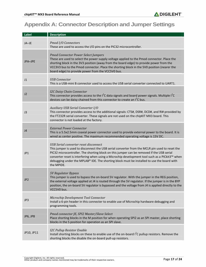
Appendix A: Connector Description and Jumper Settings
Label Description
JA–JE Pmod I/O Connectors These are used to access the I/O pins on the PIC32 microcontroller.
JPA–JPE
Pmod Connector Power Select Jumpers These are used to select the power supply voltage applied to the Pmod connector. Place the shorting block in the 3V3 position (away from the board edge) to provide power from the VCC3V3 bus to the Pmod connector. Place the shorting block in the 5V0 position (nearer the board edge) to provide power from the VCC5V0 bus.
J1 USB Connector This is a USB-mini B connector used to access the USB serial converter connected to UART1.
J2 I2C Daisy Chain Connector This connector provides access to the I
2C data signals and board power signals. Multiple I
2C
devices can be daisy chained from this connector to create an I2C bus.
J3
Auxiliary USB Serial Converter I/O This connector provides access to the additional signals: CTS#, DSR#, DCD#, and RI# provided by the FT232R serial converter. These signals are not used on the chipKIT MX3 board. This connector is not loaded at the factory.
J4 External Power Connector This is a 5.5x2.5mm coaxial power connector used to provide external power to the board. It is wired as center positive. The maximum recommended operating voltage is 15V DC.
JP1
USB Serial converter reset disconnect This jumper is used to disconnect the USB serial converter from the MCLR pin used to reset the PIC32 microcontroller. The shorting block on this jumper can be removed if the USB serial converter reset is interfering when using a Microchip development tool such as a PICkit3™ when debugging under the MPLAB® IDE. The shorting block must be installed to use the board with the MPIDE.
JP2
5V Regulator Bypass This jumper is used to bypass the on-board 5V regulator. With the jumper in the REG position, the external voltage applied at J4 is routed through the 5V regulator. If the jumper is in the BYP position, the on-board 5V regulator is bypassed and the voltage from J4 is applied directly to the VCC5V0 bus.
JP3 Microchip Development Tool Connector Install a 6-pin header in this connecter to enable use of Microchip hardware debugging and programming tools.
JP6, JP8 Pmod connector JE, SPI2 Master/Slave Select Place shorting blocks in the M position for when operating SPI2 as an SPI master, place shorting blocks in the S position for operation as an SPI slave.
JP10, JP11 I2C Pullup Resistor Enable Install shorting blocks on these to enable use of the on-board I
2C pullup resistors. Remove the
shorting blocks the disable the on-board pull-up resistors.
chipKIT™ MX3 Board Reference Manual
Copyright Digilent, Inc. All rights reserved. Other product and company names mentioned may be trademarks of their respective owners. Page 18 of 24
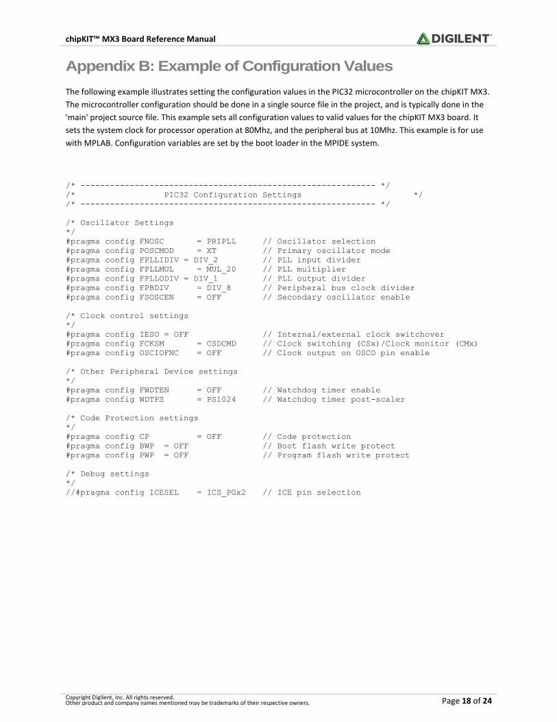
Appendix B: Example of Configuration Values
The following example illustrates setting the configuration values in the PIC32 microcontroller on the chipKIT MX3.
The microcontroller configuration should be done in a single source file in the project, and is typically done in the
'main' project source file. This example sets all configuration values to valid values for the chipKIT MX3 board. It
sets the system clock for processor operation at 80Mhz, and the peripheral bus at 10Mhz. This example is for use
with MPLAB. Configuration variables are set by the boot loader in the MPIDE system.
/* ------------------------------------------------------------ */
/* PIC32 Configuration Settings */
/* ------------------------------------------------------------ */
/* Oscillator Settings
*/
#pragma config FNOSC = PRIPLL // Oscillator selection
#pragma config POSCMOD = XT // Primary oscillator mode
#pragma config FPLLIDIV = DIV_2 // PLL input divider
#pragma config FPLLMUL = MUL_20 // PLL multiplier
#pragma config FPLLODIV = DIV_1 // PLL output divider
#pragma config FPBDIV = DIV_8 // Peripheral bus clock divider
#pragma config FSOSCEN = OFF // Secondary oscillator enable
/* Clock control settings
*/
#pragma config IESO = OFF // Internal/external clock switchover
#pragma config FCKSM = CSDCMD // Clock switching (CSx)/Clock monitor (CMx)
#pragma config OSCIOFNC = OFF // Clock output on OSCO pin enable
/* Other Peripheral Device settings
*/
#pragma config FWDTEN = OFF // Watchdog timer enable
#pragma config WDTPS = PS1024 // Watchdog timer post-scaler
/* Code Protection settings
*/
#pragma config CP = OFF // Code protection
#pragma config BWP = OFF // Boot flash write protect
#pragma config PWP = OFF // Program flash write protect
/* Debug settings
*/
//#pragma config ICESEL = ICS_PGx2 // ICE pin selection

chipKIT™ MX3 Board Reference Manual
Copyright Digilent, Inc. All rights reserved. Other product and company names mentioned may be trademarks of their respective owners. Page 19 of 24
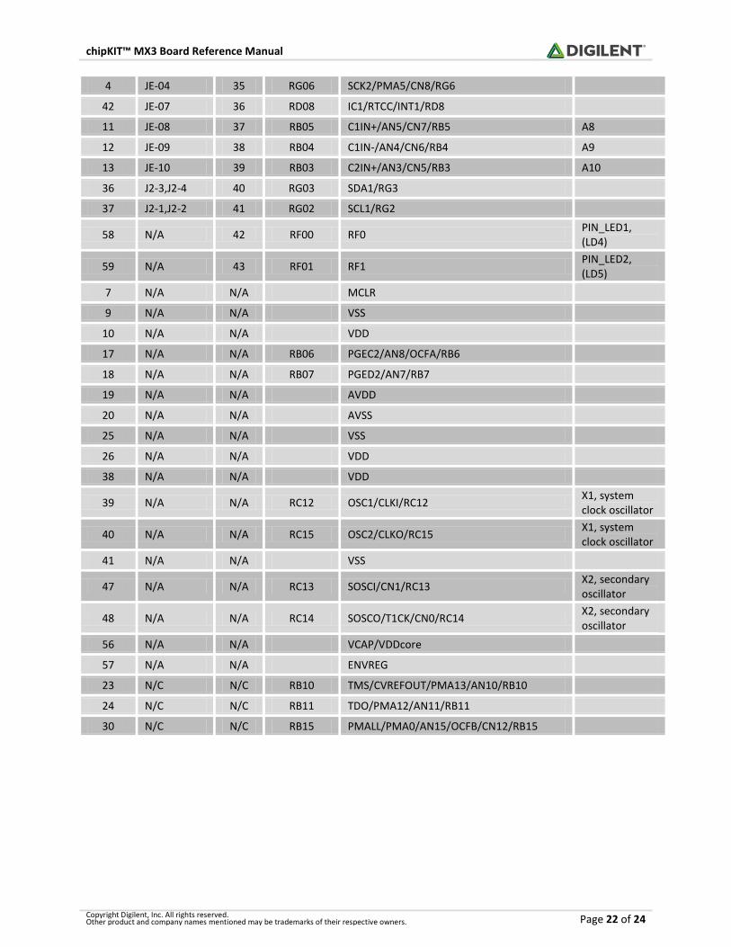
Appendix C: Connector Pinout Tables
Arranged by Microcontroller Pin Number
PIC32 Pin #
Connector Pin #
Digital Pin #
MCU Port Bit
PIC32 Signal Name Notes
1 JA-08 5 RE05 PMD5/RE5
2 JA-09 6 RE06 PMD6/RE6
3 JA-10 7 RE07 PMD7/RE7
4 JE-04 35 RG06 SCK2/PMA5/CN8/RG6
5 JE-03 34 RG07 SDI2/PMA5/CN9/RG7 JP6 in M position
6 JE-02 33 RG08 SDO2/PMA3/CN10/RG8 JP8 in M position
7 N/A N/A MCLR
8 JE-01 32 RG09 SS2/PMA2/CN11/RG9
9 N/A N/A VSS
10 N/A N/A VDD
11 JE-08 37 RB05 C1IN+/AN5/CN7/RB5 A8
12 JE-09 38 RB04 C1IN-/AN4/CN6/RB4 A9
13 JE-10 39 RB03 C2IN+/AN3/CN5/RB3 A10
14 JD-01 24 RB02 C2IN-/AN2/SS1/CN4/RB2 A4
15 JC-08 21 RB01 PGC1/AN1/VREF-/CVREF-/CN3/RB1 A3
16 JC-07 20 RB00 PGED1/PMA6/AN0/VREF+/CVREF+/CN2/RB0
A2
17 N/A N/A RB06 PGEC2/AN8/OCFA/RB6
18 N/A N/A RB07 PGED2/AN7/RB7
19 N/A N/A AVDD
20 N/A N/A AVSS
21 JC-01 16 RB08 U2CTS/C1OUT/AN8/RB8 A0
22 JD-04 27 RB09 PMA7/C2OUT/AN9/RB9 A5
23 N/C N/C RB10 TMS/CVREFOUT/PMA13/AN10/RB10
24 N/C N/C RB11 TDO/PMA12/AN11/RB11
25 N/A N/A VSS
26 N/A N/A VDD
27 JD-07 28 RB12 TCK/PMA11/AN12/RB12 A6
28 JD-10 31 RB13 TDI/PMA10/AN13/RB13 A7
29 JC-04 19 RB14 PMALH/PMA1/U2RTS/AN14/RB14 A1
30 N/C N/C RB15 PMALL/PMA0/AN15/OCFB/CN12/RB15
31 JC-03 18 RF04 PMA9/U2RX/SDA2/CN17/RF4
32 JC-02 17 RF05 PMA8/U2TX/SCL2/CN18/RF5
33 JB-02 9 RF03 U1TX/SDO1/RF3
34 JB-03 10 RF02 U1RX/SDI1/RF2
chipKIT™ MX3 Board Reference Manual
Copyright Digilent, Inc. All rights reserved. Other product and company names mentioned may be trademarks of their respective owners. Page 20 of 24
35 JB-04 11 RF06 U1RTS/BCLK1/SCK1/INT0/RF6
36 J2-3,J2-4 40 RG03 SDA1/RG3
37 J2-1,J2-2 41 RG02 SCL1/RG2
38 N/A N/A VDD
39 N/A N/A RC12 OSC1/CLKI/RC12 X1, system clock oscillator
40 N/A N/A RC15 OSC2/CLKO/RC15 X1, system clock oscillator
41 N/A N/A VSS
42 JE-07 36 RD08 IC1/RTCC/INT1/RD8
43 JB-01 8 RD09 IC2/U1CTS/INT2/RD9
44 JD-03 26 RD10 IC3/PMCS2/PMA15/INT3/RD10
45 JD-09 30 RD11 IC4/PMCS1/PMA14/INT4/RD11
46 JC-09 22 RD00 OC1/RD0 PIN_OC1
47 N/A N/A RC13 SOSCI/CN1/RC13 X2, secondary oscillator
48 N/A N/A RC14 SOSCO/T1CK/CN0/RC14 X2, secondary oscillator
49 JC-10 23 RD01 OC2/RD1 PIN_OC2
50 JD-02 25 RD02 OC3/RD2 PIN_OC3
51 JD-08 29 RD03 OC4/RD3 PIN_OC4
52 JB-09 14 RD04 PMWR/OC5/IC5/CN13/RD4 PIN_OC5
53 JB-08 13 RD05 PMRD/CN14/RD5
54 JB-07 12 RD06 CN15/RD6
55 JB-10 15 RD07 CN16/RD7
56 N/A N/A VCAP/VDDcore
57 N/A N/A ENVREG
58 N/A 42 RF00 RF0 PIN_LED1, (LD4)
59 N/A 43 RF01 RF1 PIN_LED2, (LD5)
60 JA-01 0 RE00 PMD0/RE0
61 JA-02 1 RE01 PMD1/RE1
62 JA-03 2 RE02 PMD2/RE2
63 JA-04 3 RE03 PMD3/RE3
64 JA-07 4 RE04 PMD4/RE4

chipKIT™ MX3 Board Reference Manual
Copyright Digilent, Inc. All rights reserved. Other product and company names mentioned may be trademarks of their respective owners. Page 21 of 24
Arranged by Connector Pin Number and Digital Pin Number
PIC32 Pin #
Connector Pin #
Digital Pin #
MCU Port Bit
PIC32 Signal Name Notes
60 JA-01 0 RE00 PMD0/RE0
61 JA-02 1 RE01 PMD1/RE1
62 JA-03 2 RE02 PMD2/RE2
63 JA-04 3 RE03 PMD3/RE3
64 JA-07 4 RE04 PMD4/RE4
1 JA-08 5 RE05 PMD5/RE5
2 JA-09 6 RE06 PMD6/RE6
3 JA-10 7 RE07 PMD7/RE7
43 JB-01 8 RD09 IC2/U1CTS/INT2/RD9
33 JB-02 9 RF03 U1TX/SDO1/RF3
34 JB-03 10 RF02 U1RX/SDI1/RF2
35 JB-04 11 RF06 U1RTS/BCLK1/SCK1/INT0/RF6
54 JB-07 12 RD06 CN15/RD6
53 JB-08 13 RD05 PMRD/CN14/RD5
52 JB-09 14 RD04 PMWR/OC5/IC5/CN13/RD4 PIN_OC5
55 JB-10 15 RD07 CN16/RD7
21 JC-01 16 RB08 U2CTS/C1OUT/AN8/RB8 A0
32 JC-02 17 RF05 PMA8/U2TX/SCL2/CN18/RF5
31 JC-03 18 RF04 PMA9/U2RX/SDA2/CN17/RF4
29 JC-04 19 RB14 PMALH/PMA1/U2RTS/AN14/RB14 A1
16 JC-07 20 RB00 PGED1/PMA6/AN0/VREF+/CVREF+/CN2/RB0 A2
15 JC-08 21 RB01 PGC1/AN1/VREF-/CVREF-/CN3/RB1 A3
46 JC-09 22 RD00 OC1/RD0 PIN_OC1
49 JC-10 23 RD01 OC2/RD1 PIN_OC2
14 JD-01 24 RB02 C2IN-/AN2/SS1/CN4/RB2 A4
50 JD-02 25 RD02 OC3/RD2 PIN_OC3
44 JD-03 26 RD10 IC3/PMCS2/PMA15/INT3/RD10
22 JD-04 27 RB09 PMA7/C2OUT/AN9/RB9 A5
27 JD-07 28 RB12 TCK/PMA11/AN12/RB12 A6
51 JD-08 29 RD03 OC4/RD3 PIN_OC4
45 JD-09 30 RD11 IC4/PMCS1/PMA14/INT4/RD11
28 JD-10 31 RB13 TDI/PMA10/AN13/RB13 A7
8 JE-01 32 RG09 SS2/PMA2/CN11/RG9
6 JE-02 33 RG08 SDO2/PMA3/CN10/RG8 JP8 in M position
5 JE-03 34 RG07 SDI2/PMA5/CN9/RG7 JP6 in M position
chipKIT™ MX3 Board Reference Manual
Copyright Digilent, Inc. All rights reserved. Other product and company names mentioned may be trademarks of their respective owners. Page 22 of 24
4 JE-04 35 RG06 SCK2/PMA5/CN8/RG6
42 JE-07 36 RD08 IC1/RTCC/INT1/RD8
11 JE-08 37 RB05 C1IN+/AN5/CN7/RB5 A8
12 JE-09 38 RB04 C1IN-/AN4/CN6/RB4 A9
13 JE-10 39 RB03 C2IN+/AN3/CN5/RB3 A10
36 J2-3,J2-4 40 RG03 SDA1/RG3
37 J2-1,J2-2 41 RG02 SCL1/RG2
58 N/A 42 RF00 RF0 PIN_LED1, (LD4)
59 N/A 43 RF01 RF1 PIN_LED2, (LD5)
7 N/A N/A MCLR
9 N/A N/A VSS
10 N/A N/A VDD
17 N/A N/A RB06 PGEC2/AN8/OCFA/RB6
18 N/A N/A RB07 PGED2/AN7/RB7
19 N/A N/A AVDD
20 N/A N/A AVSS
25 N/A N/A VSS
26 N/A N/A VDD
38 N/A N/A VDD
39 N/A N/A RC12 OSC1/CLKI/RC12 X1, system clock oscillator
40 N/A N/A RC15 OSC2/CLKO/RC15 X1, system clock oscillator
41 N/A N/A VSS
47 N/A N/A RC13 SOSCI/CN1/RC13 X2, secondary oscillator
48 N/A N/A RC14 SOSCO/T1CK/CN0/RC14 X2, secondary oscillator
56 N/A N/A VCAP/VDDcore
57 N/A N/A ENVREG
23 N/C N/C RB10 TMS/CVREFOUT/PMA13/AN10/RB10
24 N/C N/C RB11 TDO/PMA12/AN11/RB11
30 N/C N/C RB15 PMALL/PMA0/AN15/OCFB/CN12/RB15
chipKIT™ MX3 Board Reference Manual
Copyright Digilent, Inc. All rights reserved. Other product and company names mentioned may be trademarks of their respective owners. Page 23 of 24
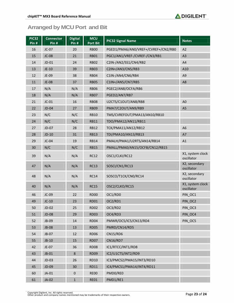
Arranged by MCU Port and Bit
PIC32 Pin #
Connector Pin #
Digital Pin #
MCU Port Bit
PIC32 Signal Name Notes
16 JC-07 20 RB00 PGED1/PMA6/AN0/VREF+/CVREF+/CN2/RB0 A2
15 JC-08 21 RB01 PGC1/AN1/VREF-/CVREF-/CN3/RB1 A3
14 JD-01 24 RB02 C2IN-/AN2/SS1/CN4/RB2 A4
13 JE-10 39 RB03 C2IN+/AN3/CN5/RB3 A10
12 JE-09 38 RB04 C1IN-/AN4/CN6/RB4 A9
11 JE-08 37 RB05 C1IN+/AN5/CN7/RB5 A8
17 N/A N/A RB06 PGEC2/AN8/OCFA/RB6
18 N/A N/A RB07 PGED2/AN7/RB7
21 JC-01 16 RB08 U2CTS/C1OUT/AN8/RB8 A0
22 JD-04 27 RB09 PMA7/C2OUT/AN9/RB9 A5
23 N/C N/C RB10 TMS/CVREFOUT/PMA13/AN10/RB10
24 N/C N/C RB11 TDO/PMA12/AN11/RB11
27 JD-07 28 RB12 TCK/PMA11/AN12/RB12 A6
28 JD-10 31 RB13 TDI/PMA10/AN13/RB13 A7
29 JC-04 19 RB14 PMALH/PMA1/U2RTS/AN14/RB14 A1
30 N/C N/C RB15 PMALL/PMA0/AN15/OCFB/CN12/RB15
39 N/A N/A RC12 OSC1/CLKI/RC12 X1, system clock oscillator
47 N/A N/A RC13 SOSCI/CN1/RC13 X2, secondary oscillator
48 N/A N/A RC14 SOSCO/T1CK/CN0/RC14 X2, secondary oscillator
40 N/A N/A RC15 OSC2/CLKO/RC15 X1, system clock oscillator
46 JC-09 22 RD00 OC1/RD0 PIN_OC1
49 JC-10 23 RD01 OC2/RD1 PIN_OC2
50 JD-02 25 RD02 OC3/RD2 PIN_OC3
51 JD-08 29 RD03 OC4/RD3 PIN_OC4
52 JB-09 14 RD04 PMWR/OC5/IC5/CN13/RD4 PIN_OC5
53 JB-08 13 RD05 PMRD/CN14/RD5
54 JB-07 12 RD06 CN15/RD6
55 JB-10 15 RD07 CN16/RD7
42 JE-07 36 RD08 IC1/RTCC/INT1/RD8
43 JB-01 8 RD09 IC2/U1CTS/INT2/RD9
44 JD-03 26 RD10 IC3/PMCS2/PMA15/INT3/RD10
45 JD-09 30 RD11 IC4/PMCS1/PMA14/INT4/RD11
60 JA-01 0 RE00 PMD0/RE0
61 JA-02 1 RE01 PMD1/RE1
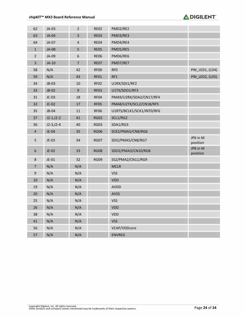
chipKIT™ MX3 Board Reference Manual
Copyright Digilent, Inc. All rights reserved. Other product and company names mentioned may be trademarks of their respective owners. Page 24 of 24
62 JA-03 2 RE02 PMD2/RE2
63 JA-04 3 RE03 PMD3/RE3
64 JA-07 4 RE04 PMD4/RE4
1 JA-08 5 RE05 PMD5/RE5
2 JA-09 6 RE06 PMD6/RE6
3 JA-10 7 RE07 PMD7/RE7
58 N/A 42 RF00 RF0 PIN_LED1, (LD4)
59 N/A 43 RF01 RF1 PIN_LED2, (LD5)
34 JB-03 10 RF02 U1RX/SDI1/RF2
33 JB-02 9 RF03 U1TX/SDO1/RF3
31 JC-03 18 RF04 PMA9/U2RX/SDA2/CN17/RF4
32 JC-02 17 RF05 PMA8/U2TX/SCL2/CN18/RF5
35 JB-04 11 RF06 U1RTS/BCLK1/SCK1/INT0/RF6
37 J2-1,J2-2 41 RG02 SCL1/RG2
36 J2-3,J2-4 40 RG03 SDA1/RG3
4 JE-04 35 RG06 SCK2/PMA5/CN8/RG6
5 JE-03 34 RG07 SDI2/PMA5/CN8/RG7 JP6 in M position
6 JE-02 33 RG08 SDO2/PMA3/CN10/RG8 JP8 in M position
8 JE-01 32 RG09 SS2/PMA2/CN11/RG9
7 N/A N/A MCLR
9 N/A N/A VSS
10 N/A N/A VDD
19 N/A N/A AVDD
20 N/A N/A AVSS
25 N/A N/A VSS
26 N/A N/A VDD
38 N/A N/A VDD
41 N/A N/A VSS
56 N/A N/A VCAP/VDDcore
57 N/A N/A ENVREG