chip manufacturing process silicon ingot slicer blank wafers 20 to 30 processing steps 8-12 in...
Post on 21-Dec-2015
229 views
TRANSCRIPT

Chip Manufacturing Process
Silicon ingot
Slicer
Blank wafers
20 to 30 processing steps
8-12 in diameter12-24 in long
< 0.1 in thick
Patterned wafer
Dicer
Individual dies
DieTester
Tested dies
Bond die topackage
Packaged dies
PartTester
Tested Packaged dies
Ship toCustomers
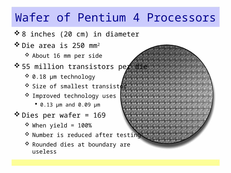
Wafer of Pentium 4 Processors 8 inches (20 cm) in diameter
Die area is 250 mm2
About 16 mm per side
55 million transistors per die 0.18 μm technology
Size of smallest transistor
Improved technology uses 0.13 μm and 0.09 μm
Dies per wafer = 169 When yield = 100%
Number is reduced after testing
Rounded dies at boundary are useless

Dramatic decrease in yield with larger dies
Yield = (Number of Good Dies) / (Total Number of Dies)
Effect of Die Size on Yield
Defective Die
Good Die
120 dies, 109 good 26 dies, 15 good
(1 + (Defect per area Die area / 2))2
1Yield =
Die Cost = (Wafer Cost) / (Dies per Wafer Yield)

Inside the Pentium 4 Processor Chip
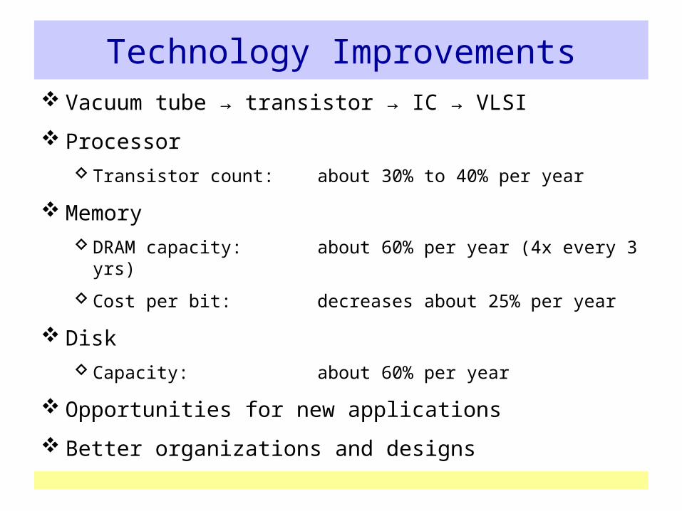
Technology Improvements Vacuum tube → transistor → IC → VLSI
Processor
Transistor count: about 30% to 40% per year
Memory
DRAM capacity: about 60% per year (4x every 3 yrs)
Cost per bit: decreases about 25% per year
Disk
Capacity: about 60% per year
Opportunities for new applications
Better organizations and designs

Growth of Capacity per DRAM Chip DRAM capacity quadrupled almost every 3 years
60% increase per year, for 20 years

Workstation Performance
More than 1000 times improvement between 1987 and 2003
Improvement is between 50% and 60% per year