chemical sensors and electronic noses based on 1-d metal oxide
TRANSCRIPT

668 IEEE TRANSACTIONS ON NANOTECHNOLOGY, VOL. 7, NO. 6, NOVEMBER 2008
Chemical Sensors and Electronic Noses Basedon 1-D Metal Oxide Nanostructures
Po-Chiang Chen, Guozhen Shen, and Chongwu Zhou, Member, IEEE
(Invited Paper)
Abstract—The detection of chemicals such as industrial gasesand chemical warfare agents is important to human health andsafety. Thus, the development of chemical sensors with high sen-sitivity, high selectivity, and rapid detection is essential and couldimpact human beings in significant ways. 1-D metal oxide nanos-tructures with unique geometric and physical properties have beendemonstrated to be important candidates as building blocks forchemical sensing applications. Chemical sensors composed of awide range of pristine 1-D metal oxide nanostructures, such asIn2O3 , SnO2 , ZnO, TiO2 , and CuO, have been fabricated, andexhibited very good sensitivity in the detection of important indus-trial gases, chemical warfare agents, and human breath. In thisreview, we provide an overview of this chemical sensing field. Vari-ous key elements of the topics will be reviewed, including 1-D metaloxide nanostructure synthesis, electronic properties of nanowire-based FETs, and their chemical sensing behaviors. In addition, thispaper provides a review of the recent development of electronicnose systems based on metal oxide nanowires, which indicate greatpotential for the improvement of sensing selectivity.
Index Terms—Electronic noses, metal oxide nanowire synthesis,nanowire chemical sensors, nanowire FETs.
I. INTRODUCTION
CHEMICAL sensors such as conductive polymer sensors[1], [2], surface acoustic wave (SAW) sensors [3], [4],
metal oxide sensors [5], [6], and microcantilever sensors [7]have important applications in the area of environmental mon-itoring, public security, automotive application, and medicaldiagnosis. Over the past few decades, researchers and engineershave dedicated their effort to develop both materials and sensorswith the characteristics of high sensitivity, good selectivity, andreliability. Till now, most commercial sensors were based onpristine or doped metal oxides due to their compatibility withhigh temperature operation [8] and great sensitivity, when com-pared with other active materials. Sensors and electronic nosesbased on metal oxide thin-film [9], [10] materials have potentialfor many applications, including the National Aeronautics andSpace Administration (NASA) space shuttle programs [11].
In 1998, Morales and Lieber demonstrated the synthesis ofsingle-crystalline Si nanowires using the laser ablation method[12]. Inspired by this work, enormous progress has been made
Manuscript received June 2, 2008; accepted September 5, 2008. First pub-lished September 26, 2008; current version published December 24, 2008. Thereview of this paper was arranged by Associate Editor J. Li.
The authors are with the Ming-Hsieh Department of Electrical Engineer-ing, University of Southern California, Los Angeles, CA 90089 USA (e-mail:[email protected]).
Color versions of one or more of the figures in this paper are available onlineat http://ieeexplore.ieee.org.
Digital Object Identifier 10.1109/TNANO.2008.2006273
in the synthesis of single-crystalline 1-D nanostructured materi-als including metals [13]–[16], III–V semiconductors [17]–[20],IV–VI semiconductors [21]–[24], and metal oxides [25]–[30].The achievements in the synthesis of nanostructured materi-als enabled scientists to explore the physical, chemical, andelectronic properties for various applications in the field of na-noelectronics [31]–[35], nanooptics [36]–[38], energy conver-sion [39]–[41], and chemical sensing [42]–[48].
With large surface-to-volume ratios and Debye length com-parable to their small size, these 1-D nanostructures have al-ready displayed superior sensitivity to surface chemical pro-cesses [49]–[54]. For example, Comini et al. [55] reported thefirst SnO2 nanobelt chemical sensor in the detection of CO,ethanol, and NO2 at elevated temperatures (300–400 ◦C). Thereported detection limit of NO2 was 0.5 ppm in the syntheticair. In the sense of practical applications, both sensitivity andselectivity are important topics to the chemical sensing com-munity. By using chemical coating [56], [57] or nanoparticledecoration [58]–[60], both device sensitivity and selectivity canbe improved. In addition, the electronic nose technique [61] isone of the approaches to solve the selectivity problem. We notethat both nanowires and conventional films based on nanostruc-tures can offer good chemical sensing performance; however,nanowires can offer certain advantages such as precise diam-eter control, easy integration into transistor configuration, andsingle-crystalline material quality.
This paper is restricted primarily to chemical sensors and elec-tronic nose systems based on 1-D semiconducting oxide nanos-tructures, including nanobelts, nanoribbons, and nanowires.Section II introduces the synthesis of 1-D metal oxide nanostruc-tures, including vapor phase growth and a laser ablation method.Section III discusses the electronic properties of metal oxidenanowires. In Section IV, chemical sensing based on different1-D metal oxides including In2O3 , ZnO, SnO2 , V2O5 , CuO,TiO2 , and WO3 will be discussed. The concept of electronicnoses and recent achievements will be studied in Section V.Finally, an outlook on other possible and new applications of1-D metal oxide nanostructure chemical sensor is presented inSection VI.
II. SYNTHESIS OF 1-D METAL OXIDE NANOSTRUCTURES
Over the past decades, a variety of approaches including elec-trochemical deposition [66], hydrothermal process [25], vaporphase growth [26], and solution phase growth [27], [28] havebeen developed to obtain bulk-quantity and high-quality 1-Dsemiconducting nanostructured materials (see Table I). Among
1536-125X/$25.00 © 2008 IEEE
Authorized licensed use limited to: University of Southern California. Downloaded on March 16, 2009 at 14:16 from IEEE Xplore. Restrictions apply.

CHEN et al.: CHEMICAL SENSORS AND ELECTRONIC NOSES BASED ON 1-D METAL OXIDE NANOSTRUCTURES 669
TABLE ISYNTHETIC METHODS DEVELOPED FOR THE SYNTHESIS OF 1-D METAL OXIDE NANOMATERIALS [62]–[65]
Fig. 1. (a) Schematic diagram of a laser-assisted chemical vapor depositionsetup. (b) Illustration of the VLS mechanism.
these methods, the vapor phase growth, governed by the vapor–liquid–solid (VLS) and vapor–solid (VS) mechanisms, is oneof the most promising methods since it provides an easy andcost-efficient way to produce numerous single-crystalline 1-Dnanomaterials with precise diameter control down to 10 nm, andthus, enables the production of nanowires on a large scale.
The laser-assisted chemical vapor deposition system is oneof the vapor phase growth methods, and a schematic diagram isshown in Fig. 1(a). Detailed experimental setup can be found inthe literature [67]. Here, we would like to use In2O3 nanowireas an example. Briefly, Si/SiO2 substrates coated with goldclusters were placed into a quartz tube at the downstream endof a furnace and the gold clusters were used as the catalysts forthe In2O3 nanowires growth. An InAs target is placed at theupper stream of the furnace and laser ablated to supply the Invapor. The approach is based on the VLS growth mechanism,where the In vapor first diffuses into the gold catalytic particlesand forms In/Au liquid drops, as shown in Fig. 1(b). Continuedaddition of In into the In/Au drops brings the alloy beyondsupersaturation and leads to the nucleation of In, which reactswith the ambient oxygen and yields In2O3 . Further supply of In
vapor feeds the In2O3 growth, and eventually the diameter of theIn2O3 nanowire is directly linked to the catalytic particle size.
After material synthesis, it is necessary to check the materialquality by SEM, X-ray diffractometer (XRD), transmitted elec-tron microscopy (TEM), and selected area electron diffraction(SAED), which will be discussed in the following sections.
A. Zinc Oxide Nanobelts
Among nanostructured semiconducting oxides, ZnO nanos-tructures have been widely explored because of their interest-ing physical and electronic properties, such as wide bandgap(∼3.37 eV at room temperature), strong piezoelectric, pyroelec-tric properties, etc. On the other hand, in the chemical sensingdirection, chemisensors built on ZnO nanostructures have alsoattracted intensive attention due to good sensitivity to importantindustrial gases, such as H2 , NH3 , CO, and H2S. It is desirable togenerate high-quality and single-crystalline ZnO nanostructuresfor the above-mentioned applications based on ZnO nanomateri-als. Thus, numerous approaches, for example, electrochemical,vapor phase growth, and liquid phase growth methods, have beendeveloped toward this direction in the past few years [68]–[70].
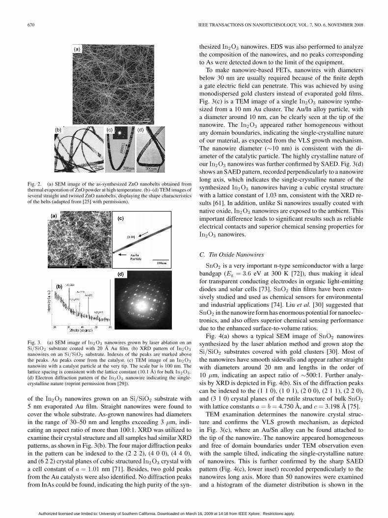
ZnO nanobelts grown on alumina plate were first reportedby Pan et al. [25] using a thermal evaporation method. Zincoxide powder without the presence of catalysts was placed in analumina tube that was inserted in a tube furnace, and the growthwas carried out under low pressure (∼300 torr) at 1400 ◦C.Without the aid of catalysts, the growth of ZnO nanobelts wasgoverned by the VS process. Fig. 2(a) is an SEM image of as-grown ZnO nanobelts, revealing wire-like morphology with thelengths of several tens to several hundred micrometers. Bothenergy dispersive X-ray spectroscopy (EDS) and XRD resultsshowed that the as-grown sample was wurtzite crystal structuredZnO nanobelts with the lattice constants of a = 3.249 A and c =5.206 A, consistent with bulk ZnO. TEM images in Fig. 2(b)–(d)exhibit their belt-like shapes with a uniform width of 50–300 nmalong the entire length, and the surface of these nanobelts areclean, suggesting the absence of any sheathed amorphous phase.
B. Indium Oxide Nanowires
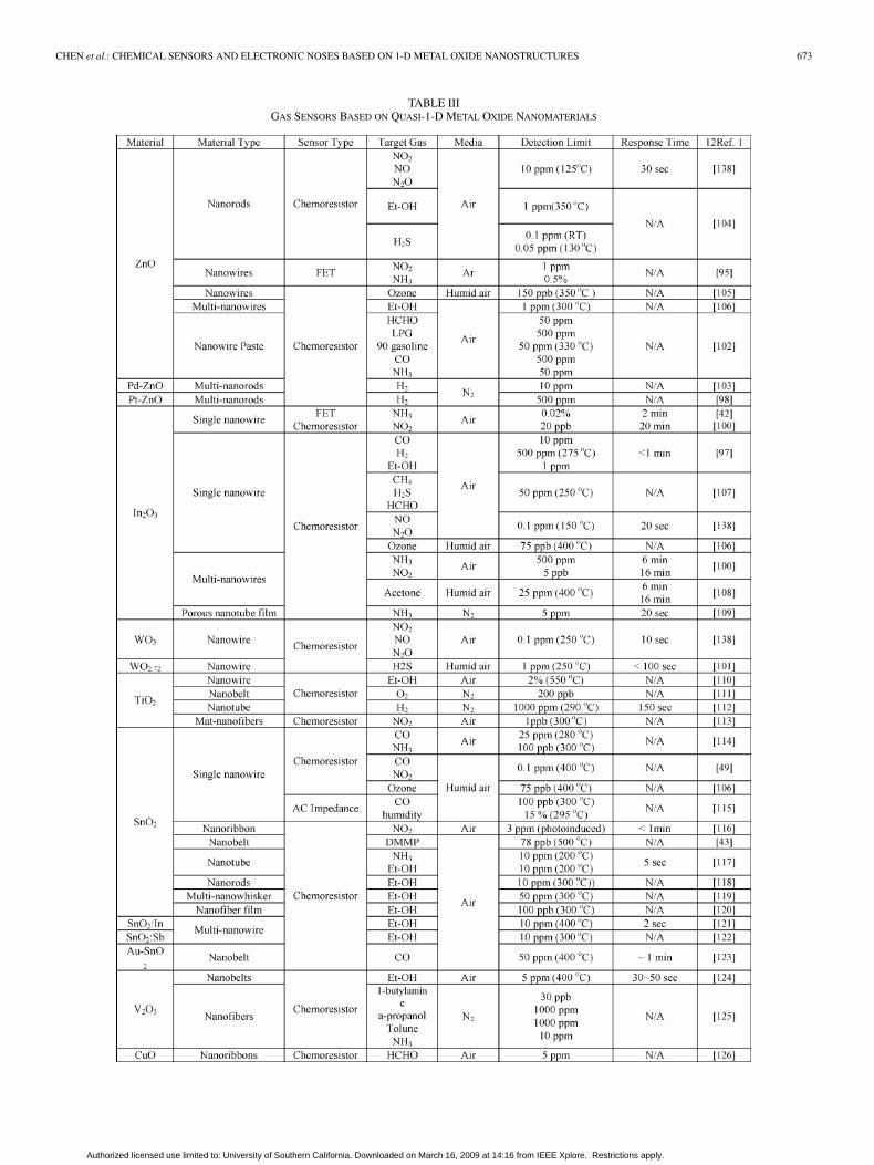
Li et al. [29] reported the synthesis of In2O3 nanowires bylaser ablation method. Fig. 3(a) shows a typical SEM image
Authorized licensed use limited to: University of Southern California. Downloaded on March 16, 2009 at 14:16 from IEEE Xplore. Restrictions apply.
670 IEEE TRANSACTIONS ON NANOTECHNOLOGY, VOL. 7, NO. 6, NOVEMBER 2008
Fig. 2. (a) SEM image of the as-synthesized ZnO nanobelts obtained fromthermal evaporation of ZnO powder at high temperature. (b)–(d) TEM images ofseveral straight and twisted ZnO nanobelts, displaying the shape characteristicsof the belts (adapted from [25] with permission).
Fig. 3. (a) SEM image of In2 O3 nanowires grown by laser ablation on anSi/SiO2 substrate coated with 20 A Au film. (b) XRD pattern of In2 O3nanowires on an Si/SiO2 substrate. Indexes of the peaks are marked abovethe peaks. Au peaks come from the catalyst. (c) TEM image of an In2 O3nanowire with a catalyst particle at the very tip. The scale bar is 100 nm. Thelattice spacing is consistent with the lattice constant (10.1 A) for bulk In2 O3 .(d) Electron diffraction pattern of the In2 O3 nanowire indicating the single-crystalline nature (reprint permission from [29]).
of the In2O3 nanowires grown on an Si/SiO2 substrate with5 nm evaporated Au film. Straight nanowires were found tocover the whole substrate. As-grown nanowires had diametersin the range of 30–50 nm and lengths exceeding 3 µm, indi-cating an aspect ratio of more than 100:1. XRD was utilized toexamine their crystal structure and all samples had similar XRDpatterns, as shown in Fig. 3(b). The four major diffraction peaksin the pattern can be indexed to the (2 2 2), (4 0 0), (4 4 0),and (6 2 2) crystal planes of cubic structured In2O3 crystal witha cell constant of a = 1.01 nm [71]. Besides, two gold peaksfrom the Au catalysts were also identified. No diffraction peaksfrom InAs could be found, indicating the high purity of the syn-
thesized In2O3 nanowires. EDS was also performed to analyzethe composition of the nanowires, and no peaks correspondingto As were detected down to the limit of the equipment.
To make nanowire-based FETs, nanowires with diametersbelow 30 nm are usually required because of the finite deptha gate electric field can penetrate. This was achieved by usingmonodispersed gold clusters instead of evaporated gold films.Fig. 3(c) is a TEM image of a single In2O3 nanowire synthe-sized from a 10 nm Au cluster. The Au/In alloy particle, witha diameter around 10 nm, can be clearly seen at the tip of thenanowire. The In2O3 appeared rather homogeneous withoutany domain boundaries, indicating the single-crystalline natureof our material, as expected from the VLS growth mechanism.The nanowire diameter (∼10 nm) is consistent with the di-ameter of the catalytic particle. The highly crystalline nature ofour In2O3 nanowires was further confirmed by SAED. Fig. 3(d)shows an SAED pattern, recorded perpendicularly to a nanowirelong axis, which indicates the single-crystalline nature of thesynthesized In2O3 nanowires having a cubic crystal structurewith a lattice constant of 1.03 nm, consistent with the XRD re-sults [61]. In addition, unlike Si nanowires usually coated withnative oxide, In2O3 nanowires are exposed to the ambient. Thisimportant difference leads to significant results such as reliableelectrical contacts and superior chemical sensing properties forIn2O3 nanowires.
C. Tin Oxide Nanowires
SnO2 is a very important n-type semiconductor with a largebandgap (Eg = 3.6 eV at 300 K [72]), thus making it idealfor transparent conducting electrodes in organic light-emittingdiodes and solar cells [73]. SnO2 thin films have been exten-sively studied and used as chemical sensors for environmentaland industrial applications [74]. Liu et al. [30] suggested thatSnO2 in the nanowire form has enormous potential for nanoelec-tronics, and also offers superior chemical sensing performancedue to the enhanced surface-to-volume ratios.
Fig. 4(a) shows a typical SEM image of SnO2 nanowiressynthesized by the laser ablation method and grown atop theSi/SiO2 substrates covered with gold clusters [30]. Most ofthe nanowires have smooth sidewalls and appear rather straightwith diameters around 20 nm and lengths in the order of10 µm, indicating an aspect ratio of ∼500:1. Further analy-sis by XRD is depicted in Fig. 4(b). Six of the diffraction peakscan be indexed to the (1 1 0), (1 0 1), (2 0 0), (2 1 1), (2 2 0),and (3 1 0) crystal planes of the rutile structure of bulk SnO2with lattice constants a = b = 4.750 A, and c = 3.198 A [75].
TEM examination determines the nanowire crystal struc-ture and confirms the VLS growth mechanism, as depictedin Fig. 3(c), where an Au/Sn alloy can be found attached tothe tip of the nanowire. The nanowire appeared homogeneousand free of domain boundaries under TEM observation evenwith the sample tilted, indicating the single-crystalline natureof nanowires. This is further confirmed by the sharp SAEDpattern (Fig. 4(c), lower inset) recorded perpendicularly to thenanowires long axis. More than 50 nanowires were examinedand a histogram of the diameter distribution is shown in the
Authorized licensed use limited to: University of Southern California. Downloaded on March 16, 2009 at 14:16 from IEEE Xplore. Restrictions apply.

CHEN et al.: CHEMICAL SENSORS AND ELECTRONIC NOSES BASED ON 1-D METAL OXIDE NANOSTRUCTURES 671
Fig. 4. (a) SEM image of tin oxide nanowires grown on an Si/SiO2 substrate.(b) XRD pattern of SnO2 nanowires obtained on Si/SiO2 substrate. (c) TEMimage of an SnO2 nanowire with a catalyst at the tip. (Lower inset) SAEDpattern taken perpendicular to the nanowire long axis. (Upper inset) Histogramsof the nanowire diameter distributions. The solid line is a Gaussian fit (reprintpermission from [30]).
upper inset of Fig. 4(c). It was found that the majority of thenanowires have diameters between 20 and 25 nm, and the dis-tribution can be well fitted with a Gaussian curve peaked at22.4 nm. The results convincingly demonstrated the precisecontrol over the diameter of the nanowires, which can be easilyachieved by using monodispersed gold clusters, an importantadvantage of the VLS approach.
III. ELECTRONIC PROPERTIES OF 1-D METAL
OXIDE NANOSTRUCTURES
With the success of producing 1-D metal oxide nanostruc-tures, 1-D nanostructure-based FETs can be made readily. InTable II, we summarize the metal-oxide-nanowire-based FETsdescribed in literature and their corresponding electronic trans-port properties. Among them, transistors made of In2O3nanowires, ZnO nanowires, and SnO2 nanowires have beenwidely reported. In comparison with other metal oxide nano-materials, as one can see, FETs fabricated with these three ma-terials exhibit high electron mobility, high transconductance,and low threshold voltage (not shown here), which are impor-tant for applications of nanoelectronics. Besides, there is stilla challenge to develop p-type metal oxide nanomaterials withgood electronic performance. Doping is a good approach toachieve p-type nanowires (Table II). For instance, Xiang et al.reported p-type ZnO nanowires with P as dopant during synthe-sis with a mobility of 1.7 cm2 /V·s and a carrier concentrationof 2.2 × 107 cm−1 .
Here, FETs built on In2O3 nanowires are used as examplesto illustrate the electronic properties of 1-D metal oxide nanos-tructures. The AFM image of Fig. 5(a) inset shows an In2O3nanowire contacted by two metallic electrodes (Ti/Au) patternedatop the Si/SiO2 substrate. These electrodes are used as thesource–drain electrodes while the silicon substrate is used as aback gate. Fig. 5(a) shows the gate-dependent I–Vds curves ofthe device measured at room temperature. With the gate voltage
varying from +15 to −10 V, the conductance of the nanowirewas gradually suppressed. This behavior is in agreement withthe well-known fact that In2O3 is an n-type semiconductor dueto the O2 deficiency [76]. Detailed analysis of the transistor datareveals an ON/OFF ratio of 2.08 × 10⁴ , a carrier concentration of2.30 nm−1 , and a mobility of 98.1 cm2 /V·s.
In addition, In2O3 is known to be one of the best candidatesfor transparent electronic applications due to its large bandgap(∼3.6 eV at room temperature). Fig. 5(b) shows the optical pho-tograph of transparent In2O3 nanowire transistors with indium-tin-oxide (ITO) electrodes patterned atop a high-k dielectriclayer (50 nm HfO2) on an ITO/glass substrate, showing verygood transparency [62]. I–Vds curves of one device with thegate voltage varied from −5 to 5 V are shown in Fig. 5(c),which displays a high ON-current of ∼3.8 µA at 2 V with zerogate voltage. Fig. 5(d) is the linear-scale and log-scale draincurrent versus gate voltage (Ids–Vg ) characteristics for the sameIn2O3 nanowire transistor at Vds = 100 mV. Detailed analysisrevealed an ON/OFF ratio ∼ 105 , a mobility of 168.7 cm2 /V·s,and a threshold voltage of −1.8 V. The electronic performanceof these transparent In2O3 nanowire transistors is comparablewith or even better than traditional In2O3 nanowire transistors,made using low-k dielectric and nontransparent electrodes.
Several approaches have been reported suggesting that theelectronic performance of nanowire-based transistors can be im-proved using some postfabrication treatments such as thermalannealing under vacuum [89] or exposure to UV ozone [90].After exposure to UV ozone for 2 min, the device perfor-mance parameters, including ON/OFF ratio, mobility, and sub-threshold slope of one In2O3 transistor, were enhanced to 106 ,514 cm2 /V·s, and 160 mV/decade, respectively.
IV. CHEMICAL SENSING BEHAVIOR OF 1-D METAL
OXIDE NANOSTRUCTURES
Both thin-film and bulk semiconducting metal oxide materi-als have been widely used for the detection of a wide range ofchemicals such as NO2 , NH3 , H2 , H2S, CO, ethanol, acetone,human breath, and humidity. The sensing mechanism of metaloxide materials mainly relies on the change of electrical con-ductivity contributed by interactions between metal oxides andsurrounding environment. The conductance of 1-D metal oxidenanomaterials can be expressed as [91]
G = n0eµπ(D − 2w)2
4l(1)
where n0 represents carrier concentration, µ represents mobility,l is the length of the nanomaterials, D is the diameter of thenanomaterials, and w is the width of surface charge region thatis related to the Debye length of the nanomaterials. The Debyelength of sensing materials can be expressed as the followingformula obtained in the Schottky approximation [92]:
w = LD
(eVs
kT
)1/2
(2)
LD =(
εε0kT
e2n0
)1/2
(3)
Authorized licensed use limited to: University of Southern California. Downloaded on March 16, 2009 at 14:16 from IEEE Xplore. Restrictions apply.

672 IEEE TRANSACTIONS ON NANOTECHNOLOGY, VOL. 7, NO. 6, NOVEMBER 2008
TABLE IISUMMARY OF THE ELECTRONIC PROPERTIES OF DIFFERENT METAL-OXIDE-NANOMATERIALS-BASED FETS
Fig. 5. (a) Gate-dependent I–V curves of a single-In2 O3 -nanowire FETrecorded at room temperature. The lower inset shows the current versus gatevoltage at Vds = 0.32 V. The gate modulated the current by five orders ofmagnitude. The upper left inset is an AFM image of the In2O3 nanowirebetween two electrodes (reprint permission from [29]). (b) Photograph of trans-parent In2O3 nanowire FETs. (c) Gate-dependent I–V curves recorded withvaried gate voltages from −5 to 5 V with step of 1 V. The inset SEM imageshows an In2 O3 nanowire between two ITO electrodes. (d) Linear-scale (blue)and log-scale (red) Ids –Vg characteristics of an In2 O3 nanowire transistor atVds ∼ 100 mV [77].
where ε0 is the absolute dielectric constant, ε is the relativedielectric permittivity of the structure, k is the Bolzmann’s con-stant, T is the temperature, and VS is the adsorbate-inducedband bending.
Generally speaking, the response of the chemoresistors inambient environment can be defined as
S =G1 − G0
G0=
4D
(w0 − w1)
=4D
(εε0
en0
)1/2 (V
1/2S0 − V
1/2S1
)(4)
where G0 and G1 are the conductance before and under expo-sure to chemicals, n0 and n1 represent the carrier concentrationbefore and under exposure to chemicals, w0 and w1 representthe width of surface charge region before and under exposureof chemicals, VS0 is the adsorbate-induced band bending due tooxygen molecule and moisture (VS0 ∼ 0.1 eV [93]) in ambientenvironment, and VS1 is the adsorbate-induced band bendingfrom exposure of chemicals (e.g., NH3 ∼ 0.25 eV [94]).
As one can see in (4), the sensing response can be clearly at-tributed to three different parts in the right term of the equation,including geometric factor (4/D), electronic transport charac-terizations of nanomaterials (εε0/en0), and adsorbate-inducedband bending (V 1/2
S0 − V1/2S1 ) due to molecular adsorptions and
reactions on metal oxide material surface. The detail of reac-tions of chemisorbed molecules on nanomaterial surface can befound in [92].
According to (4), there have been a number of approachesdeveloped to improve sensitivity, such as applying an externalgate voltage [95], [96], doping metal impurities during mate-rial growth [91], modulating operation temperature [97], andchanging the geometric structures of nanomaterials [98]. Forinstance, as one can see in Table III, the detection limit of a ZnOnanowire sensor to NO2 is tenfold better than the detection limitof a ZnO nanorod sensor because nanowire has a higher surface-to-volume ratio than a nanorod. And also an In2O3 porous nan-otube film sensor exhibits a 100-fold better sensitivity than ananowire mat sensor to ammonia at room temperature.
Typically, the detection limits of chemical sensors are also re-lated to the SNR, which has been discussed in carbon-nanotube-based chemical sensors [99]. However, until now, works ad-dressing the noise level of metal-oxide-based chemical sensorshave been lacking. This is still a task that needs to be consideredin this field.
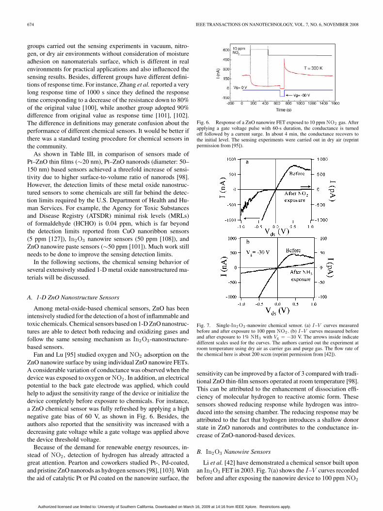
Table III summarizes some important characterizations ofmetal oxide nanostructured materials with various sensor types,different geometric structures, and measuring environments. Itis not easy to compare the sensing results from different groupsdue to different material characterizations and electronic trans-port properties, and a lack of standard procedure for gas testing.For example, instead of humid air (50% RH), some research
Authorized licensed use limited to: University of Southern California. Downloaded on March 16, 2009 at 14:16 from IEEE Xplore. Restrictions apply.
CHEN et al.: CHEMICAL SENSORS AND ELECTRONIC NOSES BASED ON 1-D METAL OXIDE NANOSTRUCTURES 673
TABLE IIIGAS SENSORS BASED ON QUASI-1-D METAL OXIDE NANOMATERIALS
Authorized licensed use limited to: University of Southern California. Downloaded on March 16, 2009 at 14:16 from IEEE Xplore. Restrictions apply.
674 IEEE TRANSACTIONS ON NANOTECHNOLOGY, VOL. 7, NO. 6, NOVEMBER 2008
groups carried out the sensing experiments in vacuum, nitro-gen, or dry air environments without consideration of moistureadhesion on nanomaterials surface, which is different in realenvironments for practical applications and also influenced thesensing results. Besides, different groups have different defini-tions of response time. For instance, Zhang et al. reported a verylong response time of 1000 s since they defined the responsetime corresponding to a decrease of the resistance down to 80%of the original value [100], while another group adopted 90%difference from original value as response time [101], [102].The difference in definitions may generate confusion about theperformance of different chemical sensors. It would be better ifthere was a standard testing procedure for chemical sensors inthe community.
As shown in Table III, in comparison of sensors made ofPt–ZnO thin films (∼20 nm), Pt–ZnO nanorods (diameter: 50–150 nm) based sensors achieved a threefold increase of sensi-tivity due to higher surface-to-volume ratio of nanorods [98].However, the detection limits of these metal oxide nanostruc-tured sensors to some chemicals are still far behind the detec-tion limits required by the U.S. Department of Health and Hu-man Services. For example, the Agency for Toxic Substancesand Disease Registry (ATSDR) minimal risk levels (MRLs)of formaldehyde (HCHO) is 0.04 ppm, which is far beyondthe detection limits reported from CuO nanoribbon sensors(5 ppm [127]), In2O3 nanowire sensors (50 ppm [108]), andZnO nanowire paste sensors (∼50 ppm [101]). Much work stillneeds to be done to improve the sensing detection limits.
In the following sections, the chemical sensing behavior ofseveral extensively studied 1-D metal oxide nanostructured ma-terials will be discussed.
A. 1-D ZnO Nanostructure Sensors
Among metal-oxide-based chemical sensors, ZnO has beenintensively studied for the detection of a host of inflammable andtoxic chemicals. Chemical sensors based on 1-D ZnO nanostruc-tures are able to detect both reducing and oxidizing gases andfollow the same sensing mechanism as In2O3-nanostructure-based sensors.
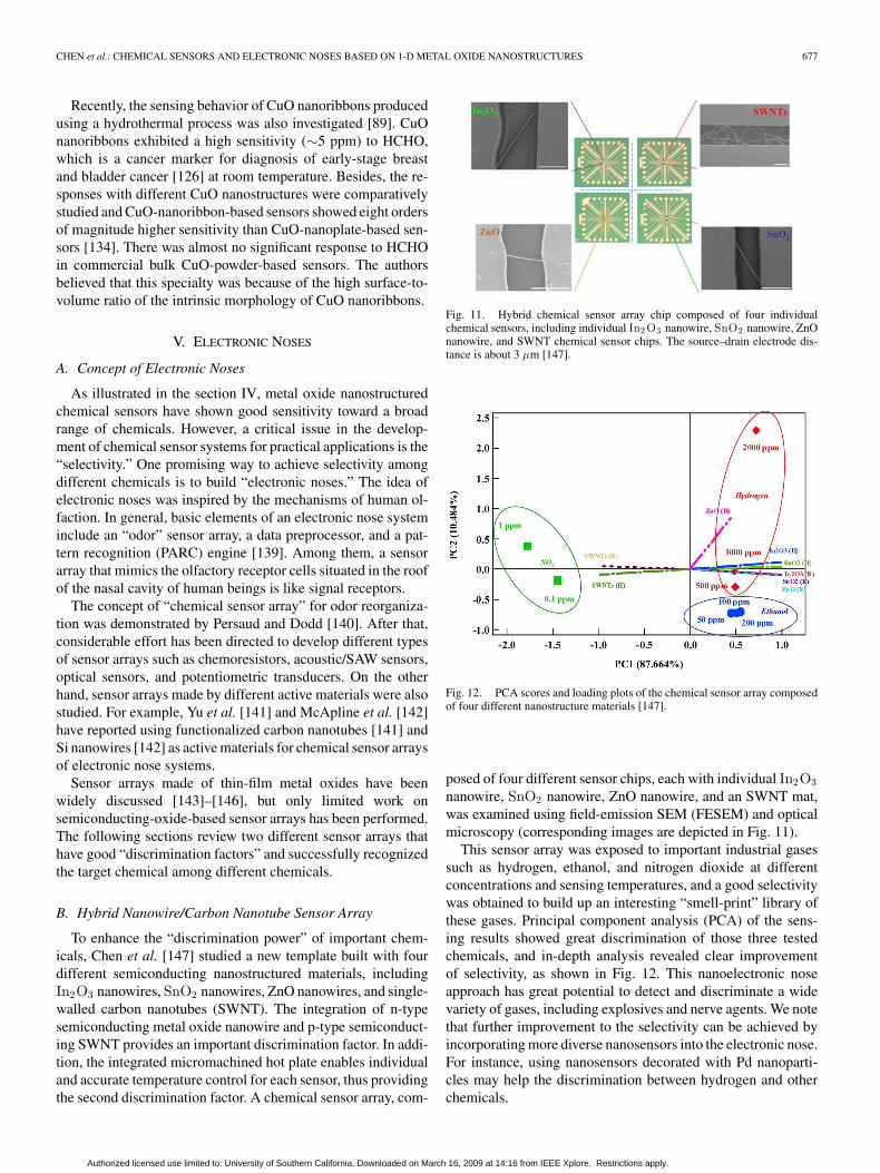
Fan and Lu [95] studied oxygen and NO2 adsorption on theZnO nanowire surface by using individual ZnO nanowire FETs.A considerable variation of conductance was observed when thedevice was exposed to oxygen or NO2 . In addition, an electricalpotential to the back gate electrode was applied, which couldhelp to adjust the sensitivity range of the device or initialize thedevice completely before exposure to chemicals. For instance,a ZnO chemical sensor was fully refreshed by applying a highnegative gate bias of 60 V, as shown in Fig. 6. Besides, theauthors also reported that the sensitivity was increased with adecreasing gate voltage while a gate voltage was applied abovethe device threshold voltage.
Because of the demand for renewable energy resources, in-stead of NO2 , detection of hydrogen has already attracted agreat attention. Pearton and coworkers studied Pt-, Pd-coated,and pristine ZnO nanorods as hydrogen sensors [98], [103]. Withthe aid of catalytic Pt or Pd coated on the nanowire surface, the
Fig. 6. Response of a ZnO nanowire FET exposed to 10 ppm NO2 gas. Afterapplying a gate voltage pulse with 60-s duration, the conductance is turnedoff followed by a current surge. In about 4 min, the conductance recovers tothe initial level. The sensing experiments were carried out in dry air (reprintpermission from [95]).
Fig. 7. Single-In2 O3 -nanowire chemical sensor. (a) I–V curves measuredbefore and after exposure to 100 ppm NO2 . (b) I–V curves measured beforeand after exposure to 1% NH3 with Vg = −30 V. The arrows inside indicatedifferent scales used for the curves. The authors carried out the experiment atroom temperature using dry air as carrier gas and purge gas. The flow rate ofthe chemical here is about 200 sccm (reprint permission from [42]).
sensitivity can be improved by a factor of 3 compared with tradi-tional ZnO thin-film sensors operated at room temperature [98].This can be attributed to the enhancement of dissociation effi-ciency of molecular hydrogen to reactive atomic form. Thesesensors showed reducing response while hydrogen was intro-duced into the sensing chamber. The reducing response may beattributed to the fact that hydrogen introduces a shallow donorstate in ZnO nanorods and contributes to the conductance in-crease of ZnO-nanorod-based devices.
B. In2O3 Nanowire Sensors
Li et al. [42] have demonstrated a chemical sensor built uponan In2O3 FET in 2003. Fig. 7(a) shows the I–V curves recordedbefore and after exposing the nanowire device to 100 ppm NO2
Authorized licensed use limited to: University of Southern California. Downloaded on March 16, 2009 at 14:16 from IEEE Xplore. Restrictions apply.

CHEN et al.: CHEMICAL SENSORS AND ELECTRONIC NOSES BASED ON 1-D METAL OXIDE NANOSTRUCTURES 675
in Ar for 5 min with 0 V applied to the gate electrode. Differentscales (left axis for the curve before the exposure and rightaxis for the curve after the exposure) were used to elucidate thechange in the current magnitude.
The I–V curve recorded before the exposure is typical forIn2O3 nanowire FETs with a well-defined linear regime and asaturation regime under the positive bias. The asymmetry in theI–V curve is due to the local gating effect, similar to the pinch-off effect of conventional silicon-based FETs [127]. After theexposure, the device showed a reduction in conductance aroundsix orders of magnitude for Vds = 0.3 V, as manifested by thedata shown in Fig. 7(a). After each exposure, the device waseasily recovered to its initial status within a short time by pump-ing down the system to vacuum followed by UV illumination todesorb the attached NO2 molecules.
The underlying physics is that UV exposure generates elec-tron and hole pairs in the nanowire, and the adsorbed NO2molecules undergo the transition from NO−
2 to NO2 by takingone hole and leave the nanowire surface. This recovery mecha-nism works for all sorts of adsorbed species such as NO2 , NH3 ,O2 , and moisture. Fig. 7(b) depicts two curves recorded beforeand after exposure to NH3 gases with the gate bias maintained at−30 V. A reduction in conductance of five orders of magnitudefor Vds = −0.3 V was obtained. The enhanced sensitivity is pri-marily attributed to the enhanced surface-to-volume ratio due tothe small diameter (10 nm) of In2O3 nanowires. An additionalreason is related to the nature of the In2O3 nanowire surfacethat can readily react with ambient species, as compared to theinert sidewall of carbon nanotubes [128].
In order to explore the detection limit and improve the deviceyield, Zhang et al. [100] reported an ultrasensitive NO2 sensorbased on In2O3 nanowire networks. Fig. 8(a) plots the changesin nanowire conductance normalized by the initial conductance(G0) at gate bias Vg = 0 V as a function of time. Six cycles weresuccessively recorded, corresponding to six different NO2 /airconcentrations ranging from 5 to 200 ppb, respectively. Themultiwire sensor showed an even lower detection limit of 5 ppb,compared to the 20 ppb limit of single-nanowire sensors[99].
Detailed examination showed a normalized conductancechange ∼20% to 5 ppb NO2 in air, with a response time of∼1000 s, defined as the time corresponding to a decrease ofthe resistance down to 80% of the original value. This roomtemperature detection limit to NO2 is the lowest level achievedso far with all metal oxide film or nanowire sensors. The au-thors attributed the improved sensitivity to the formation ofnanowire/nanowire junctions between the metal electrodes, afeature available in the multiple nanowire devices [Fig. 8(b)]but missing in the single-nanowire devices. Such junctions,when exposed to NO2 , should form a depleted layer aroundthe intersection and thus block the electron flow in a way moreprominent than the surface depletion of single nanowires withmetal contacts.
To reach practical applications of metal oxide nanowire sen-sors, operating the nanosensors at elevated temperature withminimal inconvenience and low power consumption is very im-portant. Ryu et al. proposed a facile integration of nanowire
Fig. 8. (a) Six sensing cycles of a multi-In2 O3 nanowire device, correspond-ing to NO2 concentrations of 5, 10, 20, 50, 100, and 200 ppb. (b) SEM image ofthe as-fabricated multiwire devices, where bulk quantity (102 –103 ) of In2 O3nanowires is contacted by four electrodes. The authors carried out the experi-ment at room temperature and used dry air for both carrier gas and purge gas.The flow rate of the chemicals is about 200 sccm (reprint permission from[100]).
chemical sensors with micromachined hot plates built on SiNmembranes. The details can be found in literature [97]. Fig. 9(a)is an SEM image of the active area of one chemical sensor chip,where the dashed box represents the SiN membrane and onenanowire is bridged by two electrodes that can be used as achemical sensor, as shown in Fig. 9(b).
The performance of these microelectromechanical systems(MEMS) hot plates can be evaluated by measuring the hot platetemperature as a function of the power consumption. As onecan see in Fig. 9(c), only 60 mW of power is enough to raisethe heater temperature up to 300 ◦C within 1 min, which ismuch lower than the chemical sensors based on the KAMINAtechnique [9], [10]. With the aid of micromachined hot plates,the detection limit of ethanol can be down to 1 ppm while theoperating temperature is at 275 ◦C [Fig. 9(d)].
C. 1-D SnO2 Nanostructure Sensors
SnO2 nanowires and nanobelts have been widely reportedas chemical sensors in a number of reports [129]–[131]. Thefirst SnO2 nanobelt chemical sensor was made on an aluminasubstrate by dispersing SnO2 nanobelts atop prefabricated plat-inum interdigitated electrodes on a substrate. The sensor wasemployed to detect CO and NO2 for environmental pollut-ing species and ethanol for breath analysis. In 2005, Yu et al.[43] reported a single-SnO2-nanobelt sensor integrated with
Authorized licensed use limited to: University of Southern California. Downloaded on March 16, 2009 at 14:16 from IEEE Xplore. Restrictions apply.

676 IEEE TRANSACTIONS ON NANOTECHNOLOGY, VOL. 7, NO. 6, NOVEMBER 2008
Fig. 9. (a) SEM image of the chemical sensor chip integrated on single-In2 O3nanowire and micromachined hot plates, where the dashed box indicates the SiNmembrane. (b) SEM image of a sensing device with an In2 O3 nanowire bridgingtwo electrodes. (c) Hot plate temperature as a function of the power consumptionof the Pt heater. (d) Sensing response of an In2 O3 nanowire sensor operatedat 275 ◦C to four different ethanol concentrations (1, 10, 50, and 100 ppm).The normalized conductance change (∆G/G) of an In2O3 nanowire is plottedas a function of time (d). The authors carried out the experiment at roomtemperature and used dry air for both carrier gas and purge gas (adapted from[97] with permission).
microheaters to sense dimethyl methylphosphonate (DMMP),a nerve agent simulant. The conductance of the SnO2 nanobeltsensor was reduced by 5% when the sensor was exposed to78 ppb of DMMP [Fig. 10(a)]. Recently, Wan et al. [122]proposed a high-performance ethanol senor based on branchedSnO2 /Sb-doped SnO2 nanowire films. The metallic backbonesof Sb-doped SnO2 dramatically reduced the resistance by a fac-tor of 103 and the branched structure offered more pathwaysfor electrical conduction in comparison of pure SnO2 nanowirefilms, thus significantly reducing the detectable limit of ethanolto sub-ppm at 300 ◦C.
Instead of using pristine SnO2 nanomaterials as chemicalsensors, Kolmakov et al. demonstrated an enhanced 1-D SnO2-nanostructure-based sensor with Pd nanoparticles decorated onthe surface of nanowires and nanobelts [44]. It is known thatPd can work as catalysts for oxygen dissociation. The catalyticeffect of a Pd nanoparticle and sensing capability of functional-ized SnO2 were investigated in detail. Fig. 10(b) shows differentsensing responses of Pd–SnO2 and pristine SnO2 nanostruc-tures to oxygen and hydrogen, respectively. As one can see, Pdfunctionalization leads to significant sensing response and alsoshortens the recovery time. The improvements of sensitivity canbe explained by the “spillover effect” and the “back-spillovereffect,” which are well established in catalysis literature [44].Through these two processes, the numbers of oxygen ions ad-sorbed on SnO2 surface were increased, and thus resulted inshorter response time. In addition to Pd nanoparticle decora-tion, Ag [132], Ni [91], and Au [123] nanoparticles have alsobeen reported for SnO2 nanostructure decoration, leading toimproved sensitivity of ethylene [130] and CO [122] down toseveral tens ppm.
Fig. 10. (a) Response of the SnO2 nanobelt sensor to 78 and 53 ppb DMMPbalanced with air at 500 ◦C. The applied voltage to nanobelt was 1.5 V (reprintpermission from [43]). (b) Response of a pristine SnO2 and Pd–SnO2 tosequential oxygen and hydrogen pulses at 473 (top) and 543 K (bottom). Thesensing experiments were carried out in low-pressure environment with oxygenas back ground gases. The detail can be found in [44] (reprint permissionfrom [44]).
D. Other 1-D Metal Oxide Nanostructure Sensors
In addition to the above-discussed nanomaterials, other1-D metal oxide nanostructures, such as titanium oxide (TiO2)[110], [113], [133], vanadium oxide (V2O5) [124], [125], cop-per oxide (CuO) [134], [135], and tungsten oxide (WO3) [136]–[138], have also been investigated and used as chemical sensors.
Several studies on TiO2 nanowires and nanofibers in thedetection of ethanol, hydrogen, and NO2 have been reported.Tuller et al. reported a novel electrospun method to fabricateTiO2 nanofiber mat sensors [113], which exhibited a sensi-tivity to NO2 down to ∼1 ppb at 300 ◦C. The device resis-tance was found to increase by 833% after the exposure to500 ppb NO2 . The authors stated that the sensing mechanismof TiO2 nanofibers is similar to the sensing mechanism of re-ported n-type semiconducting metal oxides. These electrospun-fabricated TiO2 nanofiber sensors were also exposed to H2 ,CH4 , and DMMP, and the sensing limits of these chemicalswere several ppm.
In the case of V2O5 nanostructures, Raible et al. reportedV2O5-nanofiber-based sensors that showed a high sensitivityof 30 ppb 1-butylamine at room temperature, and the authorssuggested that V2O5 nanofibers have a strong affinity to aminespecies [125]. In addition, Liu et al. synthesized V2O5 nanobeltsusing a hydrothermal method, and the V2O5 nanobelt chemicalsensors showed a good selectivity among ethanol vapor, H2 , andCO [125]. Since V2O5 nanostructures showed a good sensitivityand selectivity to amine and ethanol, these nanostructures mightbe utilized as components in an electronic nose system or fordiagnosis of diseases such as uremia and cancers.
Authorized licensed use limited to: University of Southern California. Downloaded on March 16, 2009 at 14:16 from IEEE Xplore. Restrictions apply.
CHEN et al.: CHEMICAL SENSORS AND ELECTRONIC NOSES BASED ON 1-D METAL OXIDE NANOSTRUCTURES 677
Recently, the sensing behavior of CuO nanoribbons producedusing a hydrothermal process was also investigated [89]. CuOnanoribbons exhibited a high sensitivity (∼5 ppm) to HCHO,which is a cancer marker for diagnosis of early-stage breastand bladder cancer [126] at room temperature. Besides, the re-sponses with different CuO nanostructures were comparativelystudied and CuO-nanoribbon-based sensors showed eight ordersof magnitude higher sensitivity than CuO-nanoplate-based sen-sors [134]. There was almost no significant response to HCHOin commercial bulk CuO-powder-based sensors. The authorsbelieved that this specialty was because of the high surface-to-volume ratio of the intrinsic morphology of CuO nanoribbons.
V. ELECTRONIC NOSES
A. Concept of Electronic Noses
As illustrated in the section IV, metal oxide nanostructuredchemical sensors have shown good sensitivity toward a broadrange of chemicals. However, a critical issue in the develop-ment of chemical sensor systems for practical applications is the“selectivity.” One promising way to achieve selectivity amongdifferent chemicals is to build “electronic noses.” The idea ofelectronic noses was inspired by the mechanisms of human ol-faction. In general, basic elements of an electronic nose systeminclude an “odor” sensor array, a data preprocessor, and a pat-tern recognition (PARC) engine [139]. Among them, a sensorarray that mimics the olfactory receptor cells situated in the roofof the nasal cavity of human beings is like signal receptors.
The concept of “chemical sensor array” for odor reorganiza-tion was demonstrated by Persaud and Dodd [140]. After that,considerable effort has been directed to develop different typesof sensor arrays such as chemoresistors, acoustic/SAW sensors,optical sensors, and potentiometric transducers. On the otherhand, sensor arrays made by different active materials were alsostudied. For example, Yu et al. [141] and McApline et al. [142]have reported using functionalized carbon nanotubes [141] andSi nanowires [142] as active materials for chemical sensor arraysof electronic nose systems.
Sensor arrays made of thin-film metal oxides have beenwidely discussed [143]–[146], but only limited work onsemiconducting-oxide-based sensor arrays has been performed.The following sections review two different sensor arrays thathave good “discrimination factors” and successfully recognizedthe target chemical among different chemicals.
B. Hybrid Nanowire/Carbon Nanotube Sensor Array
To enhance the “discrimination power” of important chem-icals, Chen et al. [147] studied a new template built with fourdifferent semiconducting nanostructured materials, includingIn2O3 nanowires, SnO2 nanowires, ZnO nanowires, and single-walled carbon nanotubes (SWNT). The integration of n-typesemiconducting metal oxide nanowire and p-type semiconduct-ing SWNT provides an important discrimination factor. In addi-tion, the integrated micromachined hot plate enables individualand accurate temperature control for each sensor, thus providingthe second discrimination factor. A chemical sensor array, com-
Fig. 11. Hybrid chemical sensor array chip composed of four individualchemical sensors, including individual In2O3 nanowire, SnO2 nanowire, ZnOnanowire, and SWNT chemical sensor chips. The source–drain electrode dis-tance is about 3 µm [147].
Fig. 12. PCA scores and loading plots of the chemical sensor array composedof four different nanostructure materials [147].
posed of four different sensor chips, each with individual In2O3nanowire, SnO2 nanowire, ZnO nanowire, and an SWNT mat,was examined using field-emission SEM (FESEM) and opticalmicroscopy (corresponding images are depicted in Fig. 11).
This sensor array was exposed to important industrial gasessuch as hydrogen, ethanol, and nitrogen dioxide at differentconcentrations and sensing temperatures, and a good selectivitywas obtained to build up an interesting “smell-print” library ofthese gases. Principal component analysis (PCA) of the sens-ing results showed great discrimination of those three testedchemicals, and in-depth analysis revealed clear improvementof selectivity, as shown in Fig. 12. This nanoelectronic noseapproach has great potential to detect and discriminate a widevariety of gases, including explosives and nerve agents. We notethat further improvement to the selectivity can be achieved byincorporating more diverse nanosensors into the electronic nose.For instance, using nanosensors decorated with Pd nanoparti-cles may help the discrimination between hydrogen and otherchemicals.
Authorized licensed use limited to: University of Southern California. Downloaded on March 16, 2009 at 14:16 from IEEE Xplore. Restrictions apply.
678 IEEE TRANSACTIONS ON NANOTECHNOLOGY, VOL. 7, NO. 6, NOVEMBER 2008
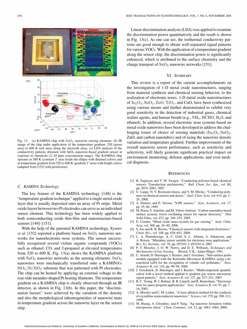
Fig. 13. (a) KAMINA chip with SnO2 nanowire sensing elements. (b) IRimage of the chip under application of the temperature gradient, 520 (greenarea) to 600 K (red area) along the electrode array. (c) LDA analysis of theconductivity patterns obtained with SnO2 -nanowire-based gradient sensor atexposure to chemicals (2–10 ppm concentration range). The KAMINA chipoperates at 580 K (constant T area inside the ellipse with dimmed colors) andat temperature gradient from 520 to 600 K (gradient T areas with bright colors)(adapted from [152] with permission).
C. KAMINA Technology
The key feature of the KAMINA technology [148] is the“temperature gradient technique” applied to a single metal oxidelayer that is usually deposited onto an array of Pt strips. Metaloxide layers between two Pt electrodes can serve as an individualsensor element. This technology has been widely applied toboth semiconducting oxide thin-film and nanostructure-basedsensors [149]–[151].
With the help of the patented KAMINA technology, Sysoevet al. [152] reported a platform based on SnO2 nanowire net-works for nanoelectronic–nose systems. The sensor success-fully recognized several violate organic compounds (VOCs)such as ethanol, CO, and 2-propanol at elevated temperaturesfrom 520 to 600 K. Fig. 13(a) shows the KAMINA platformwith SnO2 nanowire networks as the sensing elements. SnO2nanowires were mechanically transferred onto a KAMINA’sSiO2/Si/SiO2 substrate that was patterned with Pt electrodes.The chip can be heated by applying an external voltage to therear-side meander-shaped Pt heating filaments. The temperaturegradient on a KAMINA chip is clearly observed through an IRdetector, as shown in Fig. 13(b). In this paper, the “discrimi-nation factors” were achieved by the variation of the densityand also the morphological inhomogeneities of nanowire matsin temperature gradient across the nanowire layer on the sensorchip.
Linear discrimination analysis (LDA) was applied to examinethe discrimination power quantitatively and the result is shownin Fig. 13(c). As one can see, the isothermal conductivity pat-terns are good enough to obtain well-separated signal patternsfor various VOCs. With the application of a temperature gradientalong the sensor chip, the discrimination power is significantlyenhanced, which is attributed to the surface chemistry and thecharge transport of SnO2 nanowire networks [151].
VI. SUMMARY
This review is a report of the current accomplishments onthe investigation of 1-D metal oxide nanostructures, rangingfrom material synthesis and chemical sensing behavior, to therealization of electronic noses. 1-D metal oxide nanostructuresof In2O3 ,SnO2 ,ZnO,TiO2 , and CuO, have been synthesizedusing various means and further demonstrated to exhibit verygood sensitivity in the detection of industrial gases, chemicalwafare agents, and human breath (e.g., NH3 ,HCHO,H2S, andethanol). In addition, several electronic nose systems based onmetal oxide nanowires have been developed to address the chal-lenging issues of choice of sensing materials (In2O3 ,SnO2 ,ZnO, and carbon nanotubes) and of using the nanowire densityvariation and temperature gradient. Further improvement of theoverall nanowire sensor performance, such as sensitivity andselectivity, will likely generate significant practical impact onenvironment monitoring, defense applications, and even medi-cal diagnosis.
REFERENCES
[1] K. Sugiyasu and T. M. Swager, “Conducting-polymer-based chemicalsensors: Transduction mechanisms,” Bull. Chem. Soc. Jpn., vol. 80,pp. 2074–2083, 2007.
[2] U. Lange, N. V. Roznyatovskaya, and V. M. Mirsky, “Conducting poly-mers in chemical sensors and arrays,” Anal. Chim. Acta, vol. 614, pp. 1–26, 2008.
[3] A. Damico and E. Verona, “SAW sensors,” Sens. Actuators, vol. 17,pp. 55–66, 1989.
[4] M. Penza, F. Antolini, and M. Vittori-Antisari, “Carbon nanotubes-basedsurface acoustic waves oscillating sensor for vapour detection,” ThinSolid Films, vol. 472, pp. 246–252, 2005.
[5] E. Comini, “Metal oxide nano-crystals for gas sensing,” Anal. Chim.Acta, vol. 568, pp. 26–40, 2006.
[6] S. Joo and R. B. Brown, “Chemical sensors with integrated electronics,”Chem. Rev., vol. 108, pp. 638–651, 2008.
[7] L. A. Pinnaduwage, A. C. Gehl, S. L. Allman, A. Johansson, andA. Boisen, “Miniature sensor suitable for electronic nose applications,”Rev. Sci. Instrum., vol. 78, pp. 055101-1–055101-4, 2007.
[8] P. T. Moseley, J. O. W. Norris, and D. E. Williams, Techniques andMechanisms of Gas Sensing. Bristol, U.K.: Adam Hilger, 1991.
[9] C. Arnold, D. Haeringer, I. Kiselev, and J. Goschnic, “Sub-surface probemodule equipped with the Karlsruhe Micronose KAMINA using a hi-erarchical LDA for the recognition of volatile soil pollutants,” Sens.Actuators B, vol. 116, pp. 90–94, 2006.
[10] J. Goschnick, D. Haeringer, and I. Kiselev, “Multicomponent quantifi-cation with a novel method applied to gradient gas sensor microarraysignal patterns,” Sens. Actuators B, vol. 127, pp. 237–241, 2007.
[11] R. C. Young, W. J. Buttner, B. R. Linnell, and R. Ramesham, “Electronicnose for space program applications,” Sens. Actuators B, vol. 93, pp. 7–16, 2003.
[12] A. Morales and C. M. Lieber, “A laser ablation method for the synthesisof crystalline semiconductor nanowires,” Science, vol. 279, pp. 208–211,1998.
[13] M. Huang, A. Choudrey, and P. Yang, “Ag nanowire formation withinmesoporous silica,” Chem. Commun., vol. 12, pp. 1063–1064, 2000.
Authorized licensed use limited to: University of Southern California. Downloaded on March 16, 2009 at 14:16 from IEEE Xplore. Restrictions apply.
CHEN et al.: CHEMICAL SENSORS AND ELECTRONIC NOSES BASED ON 1-D METAL OXIDE NANOSTRUCTURES 679
[14] B. H. Hong, S. C. Bae, C. W. Lee, S. Jeong, and K. S. Kim, “Ultrathinsingle-crystalline silver nanowire arrays formed in an ambient solutionphase,” Science, vol. 294, pp. 348–351, 2001.
[15] Y. J. Hsu and S. Y. Lu, “Vapor–solid growth of Sn nanowires: Growthmechanism and superconductivity,” J. Phys. Chem. B, vol. 109,pp. 4398–4403, 2005.
[16] J. G. Wang, M. L. Tian, N. Kumar, and T. E. Mallouk, “Control-lable template synthesis of superconducting Zn nanowires with differ-ent microstructures by electrochemical deposition,” Nano Lett., vol. 5,pp. 1247–1253, 2005.
[17] S. Han, W. Jin, T. Tang, C. Li, D. Zhang, X. Liu, J. Han, and C. Zhou,“Controlled growth of gallium nitride single crystal nanowires using achemical vapor deposition method,” J. Mater. Res., vol. 18, pp. 245–249,2003.
[18] T. Tang, S. Han, W. Jin, X. Liu, C. Li, D. Zhang, C. Zhou, B. Chen,J. Han, and M. Meyyappan, “Synthesis and characterization of single-crystal indium nitride nanowires,” J. Mater. Res., vol. 19, pp. 423–426,2004.
[19] K. A. Dick, K. Deppert, L. S. Karlsson, W. Seifert, L. R. Wallenberg,and L. Samuelson, “Position-controlled interconnected InAs nanowirenetworks,” Nano Lett., vol. 6, pp. 2842–2847, 2006.
[20] P. Mohan, J. Motohisa, and T. Fukui, “Fabrication of InP/InAs/InP core-multishell hetrostructure nanowires by selective area metalorganic vaporphase epitaxy,” Appl. Phys. Lett., vol. 88, pp. 133105–133107, 2006.
[21] J. Zhu, H. Peng, C. K. Chan, K. Jarausch, X. F. Zhang, and Y. Cui,“Hyperbranched lead selenide nanowire networks,” Nano Lett., vol. 7,pp. 1095–1099, 2007.
[22] X. F. Qiu, Y. B. Lou, A. C. S. Samia, A. Devadoss, J. D. Burgess, S. Dayal,and C. Burda, “PbTe nanorods by sonoelectrochemistry,” Angew. Chem.Int. Ed., vol. 44, pp. 5855–5857, 2005.
[23] H. J. Chang, E. J. In, K. J. Kong, J. O. Lee, Y. M. Choi, and B. H. Ryu,“First-principles studies of SnS2 nanotubes: A potential semiconductornanowire,” J. Phys. Chem. B, vol. 109, pp. 30–32, 2005.
[24] M. J. Bierman, Y. K. A. Lau, and S. Jin, “Hyperbranched PbS and PbSenanowires and the effect of hydrogen gas on their synthesis,” Nano Lett.,vol. 7, pp. 2907–2912, 2007.
[25] Z. W. Pan, Z. R. Dai, and Z. L. Wang, “Nanobelts of semiconductingoxides,” Science, vol. 291, pp. 1947–1949, 2001.
[26] S. Han, C. Li, Z. Liu, B. Lei, D. Zhang, W. Jin, X. Liu, T. Tang, andC. Zhou, “Transition metal oxide core-shell nanowires: Generic synthesisand transport studies,” Nano Lett., vol. 4, pp. 1241–1245, 2004.
[27] L. Greene, M. Law, D. H. Tan, J. Goldberger, and P. Yang, “Generalroute to vertical ZnO nanowire arrays using textured ZnO seeds,” NanoLett., vol. 5, pp. 1231–1236, 2005.
[28] P. C. Chang, H. Y. Chen, J. S. Ye, F. S. Sheu, and J. G. Lu, “Verticallyaligned antimony nanowires as solid-state pH sensors,” Chem. Phys.Chem., vol. 8, pp. 57–61, 2007.
[29] C. Li, D. Zhang, S. Han, X. Liu, T. Tang, and C. Zhou, “Diameter-controlled growth of single-crystalline In2 O3 nanowires and their elec-tronic properties,” Adv. Mater., vol. 15, pp. 143–146, 2003.
[30] Z. Liu, D. Zhang, S. Han, C. Li, T. Tang, W. Jin, X. Liu, B. Lei, andC. Zhou, “Laser ablation synthesis and electron transport studies of tinoxide nanowires,” Adv. Mater., vol. 20, pp. 1754–1757, 2003.
[31] C. Li, B. Lei, W. Fan, D. Zhang, M. Meyyappan, and C. Zhou, “Molec-ular memory based on nanowire–molecular wire heterostructures,” J.Nanosci. Nanotechnol., vol. 7, pp. 138–150, 2007.
[32] J. Xiang, W. Lu, Y. J. Hu, Y. Wu, H. Yan, and C. M. Lieber, “Ge/Sinanowire heterostructures as high-performance field-effect transistors,”Nature, vol. 441, pp. 489–493, 2006.
[33] S. Ju, J. Li, J. Liu, P. C. Chen, Y. Ha, F. N. Ishikawa, H. K. Chang,C. Zhou, A. Facchetti, D. B. Janes, and T. J. Marks, “Transparent activematrix organic light-emitting diode displays driven by nanowire transis-tor circuitry,” Nano Lett., vol. 8, pp. 997–1004, 2008.
[34] Y. Huang, X. F. Duan, Y. Cui, L. J. Lauhon, K. H. Kim, andC. M. Lieber, “Logic gates and computation from assembled nanowirebuilding blocks,” Nano Lett., vol. 294, pp. 1313–1317, 2001.
[35] N. A. Melosh, A. Boukai, F. Diana, B. Gerardot, A. Badolato,P. M. Petroff, and J. R. Heath, “Ultrahigh-density nanowire lattices andcircuits,” Science, vol. 300, pp. 112–115, 2003.
[36] F. Qian, S. Gradecak, Y. Li, C. Y. Wen, and C. M. Lieber, “Core/multishellnanowire heterostructures as multicolor, high-efficiency light-emittingdiodes,” Nano Lett., vol. 5, pp. 2287–2291, 2005.
[37] M. H. Huang, S. Mao, H. Feick, H. Q. Yan, Y. Y. Wu, H. Kind,E. Weber, R. Russo, and P. Yang, “Room-temperature ultravioletnanowire nanolasers,” Science, vol. 292, pp. 1897–1899, 2001.
[38] A. Jamshidi, P. J. Pauzauskie, P. J. Schuck, A. T. Ohta, P. Chiou,J. Chou, P. Yang, and M. C. Wu, “Dynamic manipulation andseparation of individual semiconducting and metallic nanowires us-ing optoelectronic tweezers,” Nature Photon., vol. 2, pp. 85–89,2008.
[39] M. Law, L. E. Greene, J. C. Johnson, R. Saykally, and P. Yang, “Nanowiredye-sensitized solar cells,” Nature Mater., vol. 4, pp. 455–459, 2005.
[40] C. Levy-Clement, R. Tena-Zaera, M. A. Ryan, A. Katty, and G. Hodes,“CdSe-sensitized p-CuSCN/nanowire n-ZnO hetrojunctions,” Adv.Mater., vol. 17, pp. 1512–1515, 2005.
[41] J. B. Baxter and E. S. Aydil, “Nanowire-based dye-sensitized solar cells,”Appl. Phys. Lett., vol. 86, pp. 053114–053116, 2005.
[42] C. Li, D. Zhang, X. Liu, S. Han, T. Tang, J. Han, and C. Zhou, “In2 O3nanowires as chemical sensors,” Appl. Phys. Lett., vol. 82, pp. 1613–1616, 2003.
[43] C. Yu, Q. Hao, S. Saha, L. Shi, X. Kong, and Z. L. Wang, “Integrationof metal oxide nanobelts with microsystems for nerve agent detection,”Appl. Phys. Lett., vol. 86, pp. 063101–063103, 2005.
[44] A. Kolmakov, D. O. Klenov, Y. Lilach, S. Stemmer, and M. Moskovits,“Enhanced gas sensing by individual SnO2 nanowires and nanobeltsfunctionalized with Pd catalyst particles,” Nano Lett., vol. 5, pp. 667–673, 2005.
[45] E. Comini, G. Faglia, G. Sberveglier, D. Calestani, L. Zanotti, andM. Zha, “Tin oxide nanobelts electrical and sensing properties,” Sens.Actuators B, vol. 111–112, pp. 2–6, 2005.
[46] C. S. Rout, K. U. Kulkarni, and C. N. R. Rao, “Room temperaturehydrogen and hydrocarbon sensors based on single nanowires of metaloxides,” J. Phys. D: Appl. Phys., vol. 40, pp. 2777–2782, 2007.
[47] Q. H. Li, Y. X. Liang, Q. Wan, and T. H. Wang, “Oxygen sensingcharacteristics of individual ZnO nanowire transistors,” Appl. Phys.Lett., vol. 85, pp. 6389–6391, 2004.
[48] M. Law, H. Kind, B. Messer, F. Kim, and P. Yang, “Photochemical sens-ing of NO2 with SnO2 nanoribbon nanosensors at room temperature,”Angew. Chem. Int. Ed., vol. 41, pp. 2405–2408, 2002.
[49] J. G. Lu, P. Chang, and Z. Fan, “Quasi-one-dimensional metal oxidematerials-synthesis, properties and applications,” Mater. Sci. Eng. R,vol. 52, pp. 49–91, 2006.
[50] A. Kolmakov, X. H. Chen, and M. Moskovits, “Functionalizingnanowires with catalytic nanoparticles for gas sensing application,” J.Nanosci. Nanotechnol., vol. 8, pp. 111–121, 2008.
[51] X. J. Huang and Y. K. Choi, “Chemical sensors based on nanostructuredmaterials,” Sens. Actuators B, vol. 122, pp. 659–671, 2007.
[52] A. Kolmakov and M. Moskovits, “Chemical sensing and catalysis byone-dimensional metal-oxide nanostructures,” Annu. Rev. Mater. Res.,vol. 34, pp. 151–180, 2004.
[53] C. A. Berven and V. V. Dobrokhotov, “Towards practicable sensors usingone-dimensional nanostructures,” Int. J. Nanotechnol., vol. 5, pp. 402–449, 2008.
[54] A. Kolmakov, “Some recent trends in the fabrication, functionalisationand characterization of metal oxide nanowire gas sensors,” Int. J. Nan-otechnol., vol. 5, pp. 450–474, 2008.
[55] E. Comini, G. Faglia, G. Sberveglieri, Z. W. Pan, and Z. L. Wang,“Stable and highly sensitive gas sensors based on semiconducting oxidenanobelts,” Appl. Phys. Lett., vol. 81, pp. 1869–1871, 2002.
[56] C. Lao, Y. Li, C. P. Wong, and Z. L. Wang, “Enhancing the electrical andoptoelectronic performance of nanobelt devices by molecular surfacefunctionalization,” Nano Lett., vol. 7, pp. 1323–1328, 2007.
[57] P. Qi, O. Vermesh, M. Grecu, A. Javey, Q. Wang, and H. Dai, “Towardlarge arrays of multiplex functionalized carbon nanotube sensors forhighly sensitive and selective molecular detection,” Nano Lett., vol. 3,pp. 347–351, 2003.
[58] A. Star, V. Joshi, S. Skarupo, D. Thomas, and J.-C. P. Gabriei, “Gas sensorarray based on metal-decorated carbon nanotubes,” J. Phys. Chem. B,vol. 110, pp. 21014–21020, 2006.
[59] B. Kim, N. Park, P. S. Na, H. So, J. Kim, H. Kim, K. Kong, H. Chang,B. Ryu, Y. Choi, and J. Lee, “The effect of metal cluster coating oncarbon nanotubes,” Nanotechnology, vol. 17, pp. 496–500, 2006.
[60] Y. Sun and H. H. Wang, “High-performance, flexible hydrogne sensorsthat use carbon nanotubes decorated with palladium nanoparticles,” Adv.Mater., vol. 19, pp. 2818–2823, 2007.
[61] J. W. Gardner and P. N. Bartlett, “A brief history of electronic noses,”Sens. Actuators B, vol. 18/19, pp. 211–220, 1994.
[62] Z. R. Dai, Z. W. Pan, and Z. L. Wang, “Novel nanostructures of functionaloxides synthesized by thermal evaporation,” Adv. Funct. Mater., vol. 13,pp. 9–24, 2003.
Authorized licensed use limited to: University of Southern California. Downloaded on March 16, 2009 at 14:16 from IEEE Xplore. Restrictions apply.

680 IEEE TRANSACTIONS ON NANOTECHNOLOGY, VOL. 7, NO. 6, NOVEMBER 2008
[63] M. Kuno, “An overview of solution-based semiconductor nanowires:Synthesis and optical studies,” Phys. Chem. Chem. Phys., vol. 10,pp. 620–639, 2008.
[64] G. Z. Cao and D. W. Liu, “Template-based synthesis of nanorod,nanowire, and nanotube arrays,” Adv. Colloid Interface Sci., vol. 136,pp. 45–64, 2008.
[65] C. N. R. Rao, F. L. Deepak, G. Gundiah, and A. Govindaraja, “Inorganicnanowires,” Progr. Solid State Chem., vol. 31, pp. 5–147, 2003.
[66] K. Takahashi, S. J. Limmer, Y. Wang, and G. Z. Cao, “Synthesis andelectrochemical properties of single-crystal V2 O5 nanorod arrays bytemplate-based electrodeposition,” J. Phys. Chem. B, vol. 108, pp. 9795–9800, 2004.
[67] C. Li, D. Zhang, S. Han, X. Liu, T. Tang, B. Lei, Z. Liu, andC. Zhou, “Synthesis, electronic properties and applications of indiumoxide nanowires,” Ann. N. Y. Acad. Sci., vol. 1006, pp. 104–121, 2003.
[68] P. Chang, Z. Fan, D. Wang, W. Tseng, W. Chiou, J. Hong, and J. G. Lu,“ZnO nanowire synthesized by vapor trapping CVD method,” Chem.Mater., vol. 16, pp. 5133–5137, 2004.
[69] M. H. Wong, A. Berenov, X. Qi, M. J. Kappers, Z. H. Barber, B. Illy,Z. Lockman, M. P. Ryan, and J. L. MacManus-Driscoll, “Electrochemicalgrowth of ZnO nano-rods on polycrystalline Zn foil,” Nanotechnology,vol. 14, pp. 968–973, 2003.
[70] R. Maity, S. Das, M. K. Mitra, and K. K. Chattopadhyay, “Synthesisand characterization of ZnO nano/microfibers thin films by catalyst freesolution route,” Phys. E, Low Dimensional Syst. Nanostruct., vol. 25,pp. 605–612, 2005.
[71] R. W. G. Wyckoff, Crystal Structures. New York: Interscience, 1968.[72] P. Camagni, G. Faglia, P. Galinetto, C. Perego, G. Samoggia, and
G. Sberveglieri, “Photosensitivity activation of SnO2 thin film gas sen-sors at room temperature,” Sens. Actuators B, vol. 31, pp. 99–103,1996.
[73] N. Amin, T. Isaka, A. Yamada, and M. Konagai, “Highly efficient 1 mmthick CdTe solar cells with textured TCOs,” Solar Energy Mater. SolarCells, vol. 67, pp. 195–201, 2001.
[74] E. Comini, G. Faglia, and G. Sberveglieri, “UV light activation of tinoxide thin films for NO2 sensing at low temperatures,” Sens. ActuatorsB, vol. 78, pp. 73–77, 2001.
[75] A. A. Bolzan, C. Fong, B. J. Kennedy, and C. J. Howard, “Structuralstudies of rutile-type metal dioxides,” Acta Crystallogr. Sect. B, Struct.Sci., vol. 53, pp. 373–380, 1997.
[76] J. Tamaki, C. Naruo, Y. Yamamoto, and M. Matsuoka, “Sensing prop-erties to dilute chlorine gas of indium oxide based thin film sensorsprepared by electron beam evaporation,” Sens. Actuators B, vol. 83,pp. 190–194, 2002.
[77] P. C. Chen, F. N. Ishikawa, and C. Zhou, “High performancetransparent Indium oxide nanowire transistors,” submitted forpublication, 2007.
[78] S. Ju, K. Lee, M. Yoon, A. Facchetti, T. J. Marks, and D. B. Janes,“High performance ZnO nanowire field effect transistors with organicgate nanodielectrics: Effects of metal contacts and ozone treatment,”Nanotechnology, vol. 18, pp. 155201-1–155201-7, 2007.
[79] B. Xiang, P. Wang, X. Zhang, S. A. Dayeh, D. P. R. Aplin, C. Soci,D. Yu, and D. Wang, “Rational synthesis of p-type zinc oxide nanowirearrays using simple chemical vapor deposition,” Nano Lett., vol. 7,pp. 323–326, 2007.
[80] G.-D. Yuan, W.-J. Zhang, J.-S. Jie, X. Fan, J.-X. Tang, I. Shafiq, Z.-Z. Ye,C.-S. Lee, and S.-T. Lee, “Tunable n-type conductivity and transportproperties of Ga-doped ZnO nanowire array,” Adv. Mater., vol. 20,pp. 168–173, 2008.
[81] S. Ju, F. N. Ishikawa, P. Chen, H. Chang, and C. Zhou, “High performanceIn2 O3 nanowire transistors using organic gate nanodielectrics,” Appl.Phys. Lett., vol. 92, pp. 222105–222107, 2008.
[82] S. Ju, P. Chen, C. Zhou, Y. Ha, A. Facchetti, T. M. Marks, S. K. Kim,S. Mohammadi, and D. B. Janes, “1/f noise of SnO2 nanowire transis-tors,” Appl. Phys. Lett., vol. 92, pp. 243120–243122, 2008.
[83] E. N. Dattoli, Q. Wan, W. Guo, Y. Chen, X. Pan, and W. Lu, “Fullytransparent thin-film transistor devices based on SnO2 nanowires,” NanoLett., vol. 7, pp. 2463–2469, 2007.
[84] J. M. Baik, M. H. Kim, C. Larson, X. Chen, S. Guo, A. M. Wodtke, andM. Moskovits, “High-yield TiO2 nanowire synthesis and single nanowirefield-effect transistor fabrication,” Appl. Phys. Lett., vol. 92, pp. 242111–242113, 2008.
[85] G. T. Kim, J. Muster, V. Krstic, J. G. Park, Y. W. Park, S. Roth,and M. Burghard, “Field-effect transistor made of individual V2 O5nanofibers,” Appl. Phys. Lett., vol. 76, pp. 1875–1877, 2000.
[86] P. Chang, Z. Fan, W. Tseng, A. Rajagopal, and J. G. Lu, “Beta-Ga2 O3 nanowires: Synthesis, characterization, and p-channel field-effect transistor,” Appl. Phys. Lett., vol. 87, pp. 222102–222104,2005.
[87] Z. Fan, X. Wen, S. Yang, and J. G. Lu, “Controlled p- and n-type dopingof Fe2 O3 nanobelt field effect transistors,” Appl. Phys. Lett., vol. 87,pp. 13113–13115, 2005.
[88] Y. Lee, Y. Chueh, C. Hsieh, M. Chang, L. Chou, Z. L. Wang, Y. Lan,C. Chen, H. Kurata, and S. Isoda, “p-Type alpha-Fe2 O3 nanowires andtheir n-type transition in a reductive ambient,” Small, vol. 3, pp. 1356–1361, 2007.
[89] B. Lei, C. Li, D. Zhang, T. Tang, and C. Zhou, “Tuning electronic prop-erties of In2 O3 nanowires by doping control,” Appl. Phys. A, vol. 79,pp. 439–442, 2004.
[90] S. Ju, Y. Xuan, P. Ye, D. B. Janes, F. Ishikawa, C. Zhou, G. Lu,A. Facchetti, and T. J. Marks, “Fully transparent In2 O3 and ZnOnanowire transistors,” Nature Nanotechnol., vol. 2, pp. 378–384,2007.
[91] V. V. Sysoev, B. K. Button, K. Wepsoec, S. Dmitriev, and A. Kolmakov,“Toward the nanoscopic “electronic nose”: Hydrogen vs. carbon monox-ide discrimination with an array of individual metal oxide nano- andmesowire sensors,” Nano Lett., vol. 6, pp. 1584–1588, 2006.
[92] N. Barsan and U. Weimar, “Conduction model of metal oxide gas sen-sors,” J. Electroceram., vol. 7, pp. 143–167, 2001.
[93] S. Semancik and D. F. Cox, “Fundamental characterization of clean andgas-dosed tin oxide,” Sens. Actuators, vol. 12, pp. 101–106, 1987.
[94] M. Batzill and U. Diebold, “The surface and materials science of tinoxide,” P. Surf. Sci., vol. 79, pp. 47–154, 2005.
[95] Z. Fan and J. G. Lu, “Gate-refreshable nanowire chemical sensors,” Appl.Phys. Lett., vol. 86, pp. 123510–123512, 2006.
[96] D. Zhang, C. Li, X. Liu, S. Han, T. Tang, and C. Zhou, “Dpoing dependentNH3 sensing for indium oxide nanowires,” Appl. Phys. Lett., vol. 83,pp. 1845–1847, 2003.
[97] K. Ryu, D. Zhang, and C. Zhou, “High-performance metal oxidenanowire chemical sensors with integrated micromachined hotplates,”Appl. Phys. Lett., vol. 92, pp. 093111–093113, 2008.
[98] L. C. Tien, P. W. Sadik, D. P. Norton, L. F. Voss, S. J. Pearton,H. T. Wang, B. S. Kang, F. Ren, J. Jun, and J. Lin, “Hydrogen sens-ing at room temperature with Pt-coated ZnO thin films and nanorods,”Appl. Phys. Lett., vol. 87, pp. 222106–222108, 2005.
[99] E. S. Snow, F. K. Perkins, and J. A. Robinson, “Chemical vapor detec-tion using single-walled carbon nanotubes,” Chem. Soc. Rev., vol. 35,pp. 790–798, 2006.
[100] D. Zhang, Z. Liu, C. Li, T. Tang, X. Liu, S. Han, B. Lei, and C. Zhou,“Detection of NO2 down to ppb levels using individual and multipleIn2 O3 nanowire devices,” Nano Lett., vol. 4, pp. 1919–1924, 2004.
[101] C. S. Rout, M. Hegdge, and C. N. R. Rao, “H2 S sensors based on tungstenoxide nanostructures,” Sens. Actuators B, vol. 128, pp. 488–493, 2008.
[102] J. Xu, Y. Chen, Y. Li, and J. Shen, “Gas sensing properties of ZnOnanorods prepared by hydrothermal method,” J. Mater. Sci., vol. 40,pp. 2919–2921, 2005.
[103] H. T. Wang, B. S. Kang, F. Ren, L. C. Tien, P. W. Sadik, D. P. Norton,S. J. Pearton, and J. Lin, “Hydrogen-selective sensing at room tempera-ture with ZnO nanorods,” Appl. Phys. Lett., vol. 86, pp. 243503–243505,2005.
[104] C. Wang, X. Chu, and M. Wu, “Detection of H2 S down to ppb levelsat room temperature using sensors based on ZnO nanorods,” Sens.Actuators B, vol. 113, pp. 320–323, 2006.
[105] G. Sberveglieri, C. Baratto, E. Comini, G. Faglia, M. Ferroni, A. Pon-zoni, and A. Vomiero, “Synthesis and characterization of semiconductingnanowires for gas sensing,” Sens. Actuators B, vol. 121, pp. 208–213,2007.
[106] Q. Wan, Q. H. Li, Y. J. Chen, T. H. Wang, X. L. He, J. P. Li, andC. L. Lin, “Fabrication and ethanol sensing characteristics of ZnOnanowire gas sensors,” Appl. Phys. Lett., vol. 84, pp. 3654–3656, 2004.
[107] P. Xu, Z. Cheng, Q. Pan, J. Xu, Q. Xiang, W. Yu, and Y. Chu, “High as-pect ratio In2 O3 nanowires: Synthesis, mechanism and NO2 gas-sensingproperties,” Sens. Actuators B, vol. 130, pp. 802–808, 2008.
[108] A. Vomiero, S. Bianchi, E. Comini, G. Faglia, M. Ferroni, andG. Sberveglieri, “Controlled growth and sensing properties of In2 O3nanowires,” Crystal Growth Des., vol. 7, pp. 2500–2504, 2007.
[109] N. Du, H. Zhang, B. Chen, X. Ma, Z. Liu, J. Wu, and D. Yang, “Porousindium oxide nanotubes: Layer-by-layer assembly on carbon-nanotubetemplates and application for room-temperature NH3 gas sensors,” Adv.Mater., vol. 19, pp. 1641–1645, 2007.
Authorized licensed use limited to: University of Southern California. Downloaded on March 16, 2009 at 14:16 from IEEE Xplore. Restrictions apply.
CHEN et al.: CHEMICAL SENSORS AND ELECTRONIC NOSES BASED ON 1-D METAL OXIDE NANOSTRUCTURES 681
[110] L. Francioso, A. M. Taurino, A. Forleo, and P. Siciliano, “TiO2 nanowiresarray fabrication and gas sensing properties,” Sens. Actuators B, vol. 130,pp. 70–76, 2008.
[111] Y. Wang, G. Du, H. Liu, D. Liu, S. Qin, N. Wang, C. Hu, X. Tao, J. Jiao,J. Wang, and Z. L. Wang, “Nanostructured sheets of Ti–O nanobelts forgas sensing and antibacterial applications,” Adv. Funct. Mater., vol. 18,pp. 1131–1137, 2008.
[112] O. K. Varghese, D. Gong, M. Paulose, K. G. Ong, and C. A. Grimes,“Hydrogen sensing using titania nanotubes,” Sens. Actuators B, vol. 93,pp. 338–344, 2003.
[113] I. D. Kim, A. Rothschild, B. H. Lee, D. Y. Kim, S. M. Jo, and H. L. Tuller,“Ultrasensitive chemiresistors based on electrospun TiO2 nanofibers,”Nano Lett., vol. 6, pp. 2009–2013, 2006.
[114] D. C. Meier, S. Semancik, B. Button, E. Strelcov, and A. Kolmakov,“Coupling nanowire chemiresistors with MEMS microhotplate gas sens-ing platforms,” Appl. Phys. Lett., vol. 91, pp. 63118–63120, 2007.
[115] F. Hernandez-Ramırez, A. Tarancon, O. Casals, J. Arbiol, A. Romano-Rodrıguez, and J. R. Morante, “High response and stability in CO andhumidity measures using a single SnO2 nanowire,” Sens. Actuators B,vol. 121, pp. 3–17, 2007.
[116] M. Law, H. Kind, B. Messer, F. Kim, and P. Yang, “Photochemical sens-ing of NO2 with SnO2 nanoribbon nanosensors at room temperature,”Angew. Chem. Int. Ed., vol. 41, pp. 2405–2408, 2002.
[117] G. X. Wang, J. S. Park, M. S. Park, and X. L. Gou, “Synthesis and highgas sensitivity of tin oxide nanotubes,” Sens. Actuators B, vol. 131,pp. 313–317, 2008.
[118] Y. J. Chen, L. Nie, X. Y. Xue, Y. G. Wang, and T. H. Wang, “Linear ethanolsensing of SnO2 nanorods with extremely high sensitivity,” Appl. Phys.Lett., vol. 88, pp. 83105–83107, 2006.
[119] Z. Ying, Q. Wan, Z. T. Song, and S. L. Feng, “SnO2 nanowhiskersand their ethanol sensing characteristics,” Nanotechnology, vol. 15,pp. 1682–1684, 2004.
[120] Y. Zhang, X. Ha, J. Li, Z. Miao, and F. Huang, “Fabrication and ethanol-sensing properties of micro gas sensor based on electrospun SnO2nanofibers,” Sens. Actuators B, vol. 132, pp. 67–73, 2008.
[121] X. Y. Xue, Y. J. Chen, Y. G. Liu, S. L. Shi, Y. G. Wang, and T. H. Wang,“Synthesis and ethanol sensing properties of indium-doped thin oxidenanowires,” Appl. Phys. Lett., vol. 88, pp. 201907–201909, 2006.
[122] Q. Wan, J. Huang, Z. Xie, T. Wang, E. N. Dattoli, and W. Lu, “BranchedSnO2 nanowires on metallic nanowire backbones for ethanol sensorsapplication,” Appl. Phys. Lett., vol. 92, pp. 102101–102103, 2008.
[123] L. H. Qian, K. Wang, Y. Li, H. T. Fang, Q. H. Lu, and X. L. Ma, “COsensor based on Au-decorated SnO2 nanobelt,” Mater. Chem. Phys.,vol. 100, pp. 82–84, 2006.
[124] J. Liu, X. Wang, Q. Peng, and Y. Li, “Vanadium pentoxide nanobelts:Highly selective and stable ethanol sensor materials,” Adv. Mater.,vol. 17, pp. 764–767, 2005.
[125] I. Raible, M. Burghard, U. Schlecht, A. Yasuda, and T. Vossmeyer,“V2 O5 nanofibers: Novel gas sensors with extremely high sensitivityand selectivity to amines,” Sens. Actuators B, vol. 106, pp. 730–735,2005.
[126] L. C. Short and T. Benter, “Selective measurement of HCHO in urineusing direct liquid-phase fluorimetric analysis,” Clin. Chem. Lab. Med.,vol. 43, pp. 178–182, 2005.
[127] S. Sze, Physics of Semiconductor Devices. New York: Wiley, 1981.[128] C. Zhou, J. Kong, E. Yenilmez, and H. Dai, “Modulated chemical doping
of individual carbon nanotubes,” Science, vol. 290, pp. 1552–1555, 2000.[129] B. Panchapakesan, R. Cavicchi, S. Semancik, and D. L. DeVoe, “Sen-
sitivity, selectivity and stability of tin oxide nanostructures on largearea arrays of microhotplates,” Nanotechnology, vol. 17, pp. 415–425,2006.
[130] T. G. G. Maffeis, G. T. Owen, M. W. Penny, T. K. H. Starke, S. A. Clark,H. Ferkel, and S. P. Wilks, “Nano-crystalline SnO2 gas sensor responseto O-2 and CH4 at elevated temperature investigated by XPS,” Surf. Sci.,vol. 520, pp. 29–34, 2002.
[131] A. Helwig, G. Muller, G. Sberveglieri, and G. Faglia, “Gas responsetimes of nano-scale SnO2 gas sensors as determined by the moving gasoutlet technique,” Sens. Actuators B, vol. 126, pp. 174–180, 2007.
[132] X. H. Chen and M. Moskovits, “Observing catalysis through theagency of the participating electrons: Surface-chemistry-induced cur-rent changes in a tin oxide nanowire decorated with silver,” Nano Lett.,vol. 7, pp. 807–812, 2007.
[133] W. P. Tai and J. H. Oh, “Fabrication and humidity sensing propertiesof nanostructured TiO2 –SnO2 thin films,” Sens. Actuators B, vol. 85,pp. 154–157, 2002.
[134] X. Gou, G. Wang, J. Yang, J. Park, and D. Wexler, “Chemical synthesis,characterization and gas sensing performance of copper oxide nanorib-bons,” J. Mater. Chem., vol. 18, pp. 965–969, 2008.
[135] C. Wang, X. Q. Fu, X. Y. Xue, Y. G. Wang, and T. H. Wang, “Surfaceaccumulation conduction controlled sensing characteristic of p-type CuOnanorods induced by oxygen adsorption,” Nanotechnology, vol. 18,pp. 145506–145510, 2007.
[136] J. Polleux, A. Gurlo, N. Barsan, U. Weimar, M. Antonietti, andM. Niederberger, “Template-free synthesis and assembly of single-crystalline tungsten oxide nanowires and their gas-sensing properties,”Angew. Chem. Int. Ed., vol. 45, pp. 261–265, 2006.
[137] C. S. Rout, K. Ganesh, A. Govindaraj, and C. N. R. Rao, “Sensors forthe nitrogen oxides, NO2 , NO, and N2 O, based on In2 O3 and WO3nanowires,” Appl. Phys. A, vol. 85, pp. 241–246, 2006.
[138] Y. S. Kim, S. C. Ha, and K. Kim, “Room-temperature semiconductor gassensor based on nonstoichiometric tungsten oxide nanorod film,” Appl.Phys. Lett., vol. 86, pp. 213105-1–213105-3, 2005.
[139] M. A. Craven, J. W. Gardner, and P. N. Bartlett, “Electronic noses—Development and future prospects,” Trends Anal. Chem., vol. 15,pp. 486–493, 1996.
[140] K. Persaud and G. H. Dodd, “Analysis of discrimination mechanisms ofthe mammalian olfactory system using a model nose,” Nature, vol. 299,pp. 352–355, 1982.
[141] Y. Lu, C. Partridge, M. Meyyappan, and J. Li, “A carbon nanotubesensor array for sensitive gas discrimination using principal componentanalysis,” J. Electroanal. Chem., vol. 593, pp. 105–110, 2006.
[142] M. C. McApline, H. Ahmad, D. Wang, and J. R. Heath, “Highly orderednanowire arrays on plastic substrates for ultrasensitive flexible chemicalsensors,” Nature Mater., vol. 6, pp. 1–6, 2007.
[143] P. Althainz, A. Dahlke, M. Frietsch-Klarhof, J. Goschnick, andH. J. Ache, “Reception tuning of gas-sensor microsystem by selectivecoating,” Sens. Actuators B, vol. 24/25, pp. 366–369, 1995.
[144] J. Folch, X. G. Capdevila, M. Segarra, and J. R. Morante, “Solid elec-trolyte multisensor system for detecting O2 , CO, and NO2 ,” J. Elec-trochem. Soc., vol. 154, pp. J201–J208, 2007.
[145] P. T. Moseley, “New trends and future prospects of thick- and thin-filmgas sensors,” Sens. Actuators B, vol. 3, pp. 167–174, 1991.
[146] D. Then, A. Vidic, and C. H. Ziegler, “A highly sensitive self-oscillating cantilever array for the quantitative and qualitative analy-sis of organic vapor mixtures,” Sens. Actuators B, vol. 117, pp. 1–9,2006.
[147] P. C. Chen, F. N. Ishikawa, H. K. Chang, K. Ryu, and C. Zhou, “Nanoelectronic nose: A hybrid nanowire/carbon nanotube sensor array withintegrated micromachined hotplates for sensitive gas discrimination,”submitted for publication.
[148] P. Althainz and J. Goschnick, “Sensor for reducing or oxidizing gases,”U.S. Patent 5 783 154, 1998.
[149] C. Arnold, M. Harms, and J. Goschnick, “Air quality monitoring and firedetection with the Karlsruhe electronic micronose KAMINA,” IEEESens. J., vol. 2, no. 3, pp. 179–188, Jun. 2002.
[150] V. V. Sysoev, I. Kiselev, M. Frietsch, and J. Goschnick, “Temperaturegradient effect on gas discrimination power of a metal-oxide thin-filmsensor microarray,” Sensors, vol. 4, pp. 37–46, 2004.
[151] J. Goschnick, I. Koronczi, M. Frietsch, and I. Kiselev, “Water pollutionrecognition with the electronic nose KAMINA,” Sens. Actuators B,vol. 106, pp. 182–186, 2005.
[152] V. V. Sysoev, J. Goschnick, T. Schneider, E. Strelcov, and A. Kolmakov, “A gradient microarray electronic nose based on percolating SnO2nanowire sensing elements,” Nano Lett., vol. 7, pp. 3182–3188,2007.
Po-Chiang Chen received the B.S. degree in physicsfrom Tamkang University, Taipei, Taiwan, in 1999,and the M.S. degree in optoelectronics from the Na-tional Taipei University of Technology, Taipei, in2001. He is currently working toward the Ph.D. de-gree in chemical engineering and materials science atthe University of Southern California, Los Angeles.
His current research interests include the deviceapplications based on 1-D nanomaterials, includingchemical sensors, transparent electronics, and energyconversion and storage devices.
Authorized licensed use limited to: University of Southern California. Downloaded on March 16, 2009 at 14:16 from IEEE Xplore. Restrictions apply.

682 IEEE TRANSACTIONS ON NANOTECHNOLOGY, VOL. 7, NO. 6, NOVEMBER 2008
Guozhen Shen received the B.S. degree in chemi-cal education from Anhui Normal University, Wuhu,China, in 1999, and the Ph.D. degree in chemistryfrom the University of Science and Technology ofChina, Hefei, China, in 2003.
He was a Postdoctoral Researcher at Hanyang Uni-versity, Korea, in 2004. He then joined the NationalInstitute for Materials Science, Japan, as a VisitingResearcher. He is currently a Research Scientist atthe University of Southern California, Los Angeles.He is the author or coauthor of more than 90 research
articles, five book chapters, and several patents. His current research interestsinclude the synthesis and characterization of 1-D nanostructures and their deviceapplication in electronics and optoelectronics.
Chongwu Zhou received the B.S. degree from theUniversity of Science and Technology of China,Hefei, China, in 1993 and the Ph.D. degree in elec-trical engineering from Yale University, New Haven,CT, in 1999.
He was a Postdoctoral Research Fellow at Stan-ford University from November 1998 to June 2000. InSeptember 2000, he joined the University of SouthernCalifornia (USC), Los Angeles. His research grouphas been working at the forefront of nanoscience andnanotechnology, including synthesis and applications
of carbon nanotubes and nanowires, biosensing, and nanotherapy.Dr. Zhou has won a number of awards, including the National Science
Foundation (NSF) CAREER Award, the National Aeronautics and Space Ad-ministration (NASA) Turning Goals Into Reality (TGiR) Award, the USC Ju-nior Faculty Research Award, and the IEEE Nanotechnology Early CareerAward. He is currently an Associate Editor for the IEEE TRANSACTIONS ON
NANOTECHNOLOGY.
Authorized licensed use limited to: University of Southern California. Downloaded on March 16, 2009 at 14:16 from IEEE Xplore. Restrictions apply.