charge-based capacitance measurement circuits for
TRANSCRIPT
Charge-Based Capacitance Measurement Circuits for Interface
with Atomic Force Microscope Probes
Joseph J. Kopanski, M. Yaqub Afridi, Chong Jiang*, Michael Lorek*, and Timothy Kohler*
Semiconductor and Dimensional Metrology Division
National Institute of Standards and Technology Gaithersburg, MD 20899
Problem
Truly quantitative capacitance measurements of very small capacitors using an atomic force microscope probe to make contact have proven difficult.

APPROACH
Create CBCM circuits capable of measuring capacitances in the presence of large series and parallel stray capacitances by precisely measuring the charge transferred onto the device versus a reference. Interface the CBCM chip with an AFM tip with associated electronics needed to make quantitative capacitance measurements.

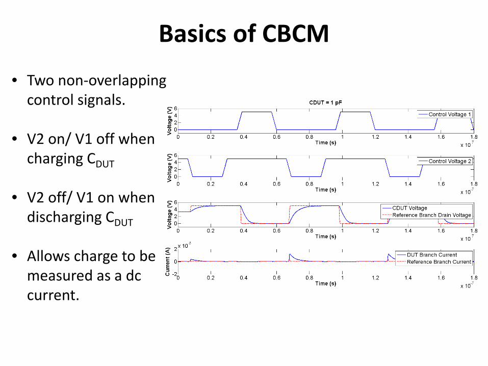
Basics of CBCM
CDUT = “Device Under Test” Capacitor Cpar=Parasitic Capacitance
CDUT Cpar Cpar
Randy Bach et al. Improvements to CBCM (Charge-Based Capacitance Measurement) for Deep Submicron CMOS Technology. Proceedings of the 7th International Symposium on Quality Electronic Design. 2006. 324-329.
• A complementary pair of transistors (or transmission gates)
• Built-in reference branch to allow separate, simultaneous measurement of stray capacitance
Basics of CBCM
• Two non-overlapping control signals.
• V2 on/ V1 off when charging CDUT
• V2 off/ V1 on when discharging CDUT
• Allows charge to be measured as a dc current.
6
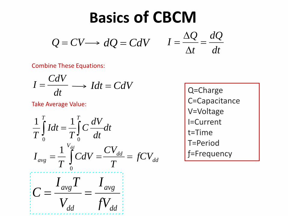
Basics of CBCM
dtdtdVC
TIdt
T
TT
∫∫ =00
11
dddd
V
avg fCVT
CVCdVT
Idd
=== ∫0
1
dtdQ
tQI =∆∆
=CVQ = CdVdQ =
CdVIdt =dt
CdVI =
dd
avg
dd
avg
fVI
VTI
C ==
Combine These Equations:
Take Average Value:
Q=Charge C=Capacitance V=Voltage I=Current t=Time T=Period ƒ=Frequency
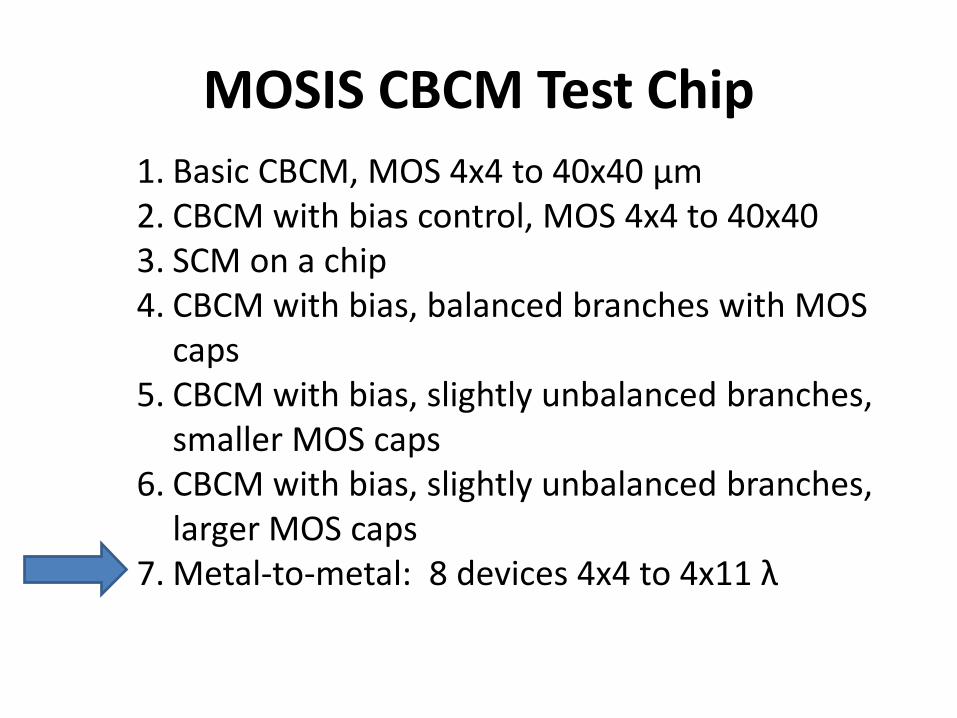
MOSIS CBCM Test Chip 1. Basic CBCM, MOS 4x4 to 40x40 µm 2. CBCM with bias control, MOS 4x4 to 40x40 3. SCM on a chip 4. CBCM with bias, balanced branches with MOS
caps 5. CBCM with bias, slightly unbalanced branches,
smaller MOS caps 6. CBCM with bias, slightly unbalanced branches,
larger MOS caps 7. Metal-to-metal: 8 devices 4x4 to 4x11 λ

Series 7 (metal-to-metal) Device Dimensions
(λ) Area (cm-2)
Capacitance (aF)
1 4 x 5 1.80 x 10⁻⁸ 191
2 5 x 4 1.80 x 10⁻⁸ 191
3 4 x 6 2.16 x 10⁻⁸ 229
4 4 x 7 2.52 x 10⁻⁸ 267
5 4 x 8 2.88 x 10⁻⁸ 305
6 4 x 9 3.24 x 10⁻⁸ 344
7 4 x 10 3.60 x 10⁻⁸ 382
8 4 x 11 3.96 x 10⁻⁸ 421
Theoretical capacitance for εlowκ = 2.4 and inter-metal oxide thickness of 200 nm
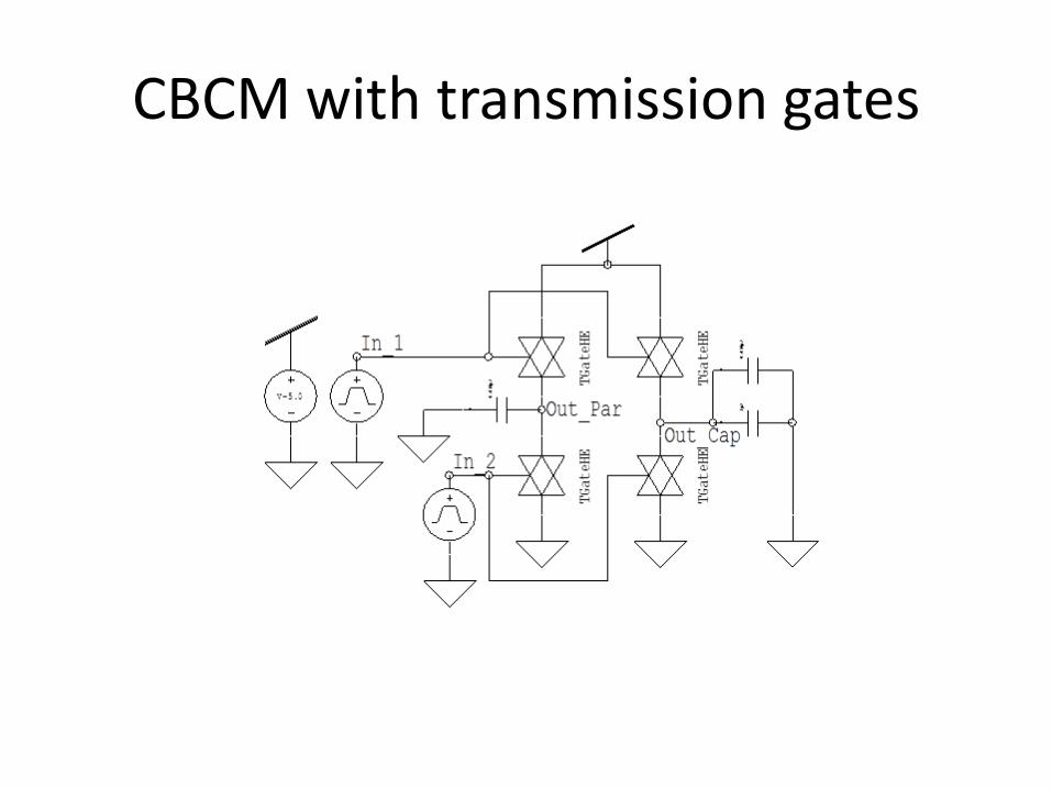
CBCM with transmission gates

Basic CBCM test Structure with metal-to-metal Capacitors
+5 V
GND
Control 1
Control 2
Reference Branch
DUT Branch
Capacitor

11
PSPICE Results: Maximum/Minimum Frequency vs. CDUT
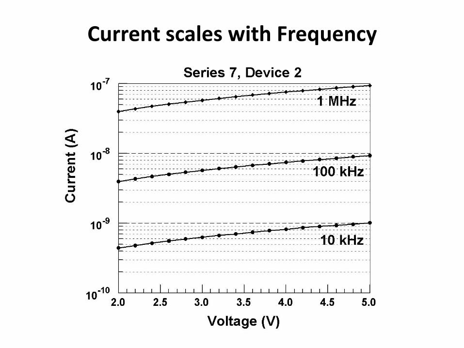
Current scales with Frequency
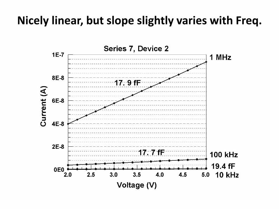
Nicely linear, but slope slightly varies with Freq.
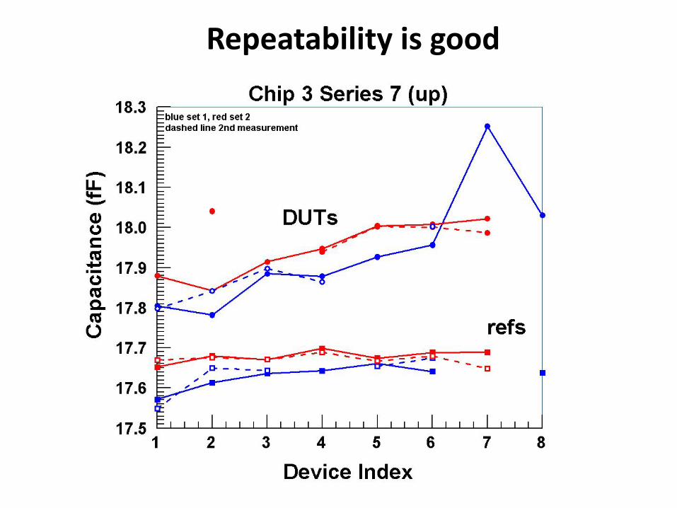
Repeatability is good
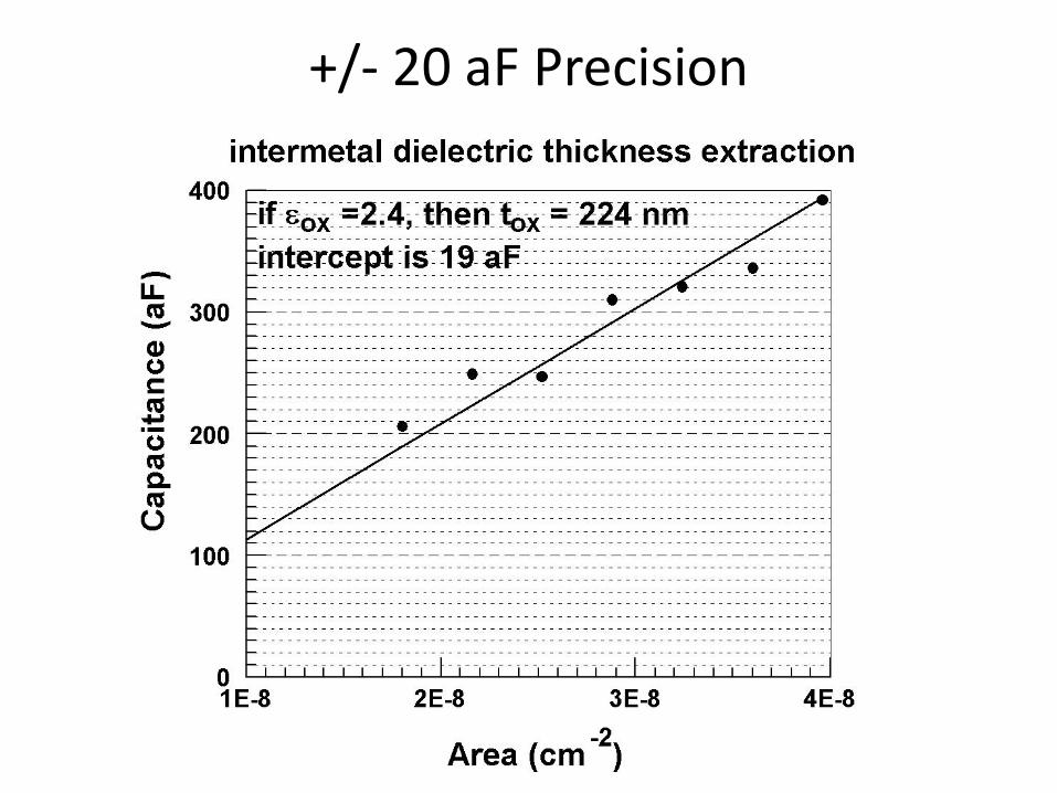
+/- 20 aF Precision
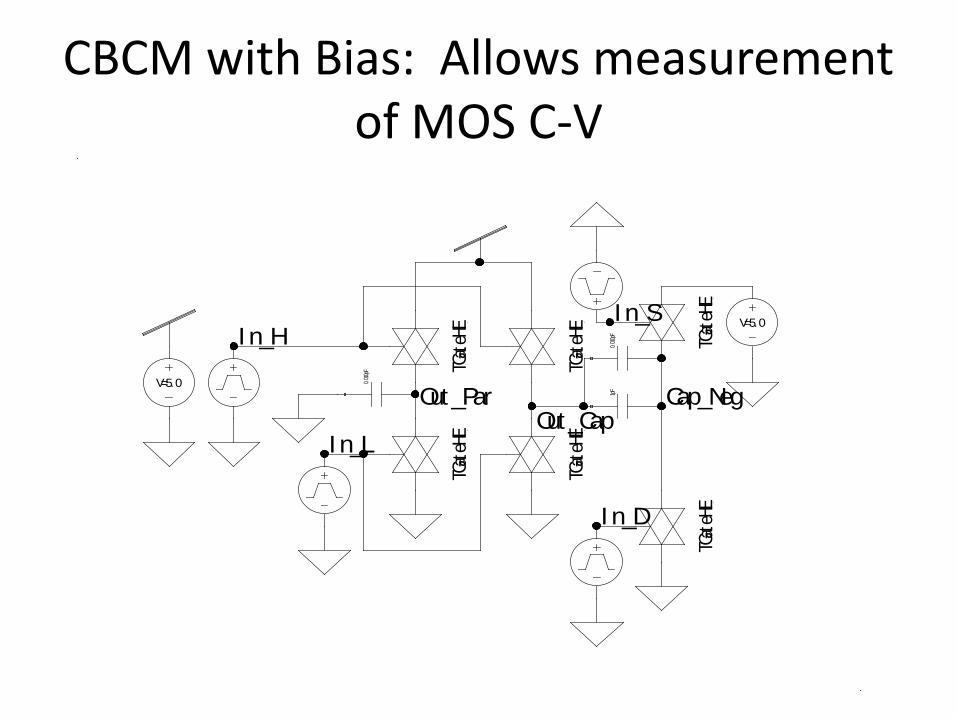
CBCM with Bias: Allows measurement of MOS C-V
I n_D
In_S
Out_ParOut_Cap
In_L
In_H
Cap_Neg
TGat
eHE
TGat
eHE
TGat
eHE
TGat
eHE
TGat
eHE
TGat
eHE V=5.0
V=5.0
0.010p
F
0.010p
F
1pF
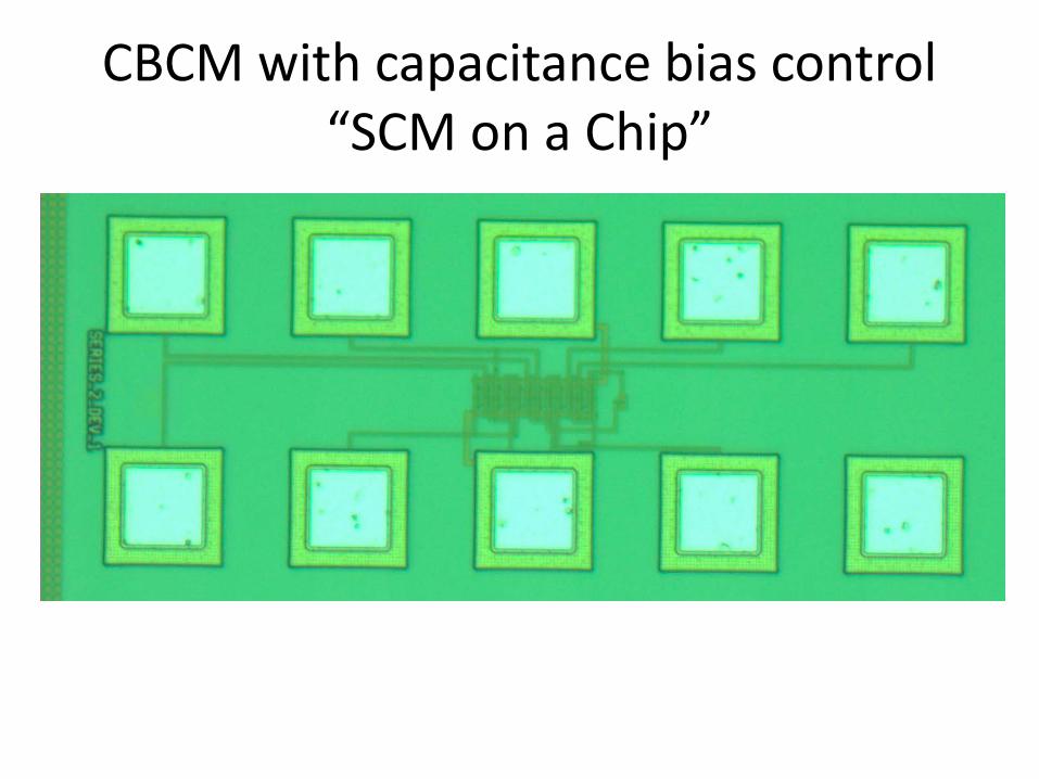
CBCM with capacitance bias control “SCM on a Chip”
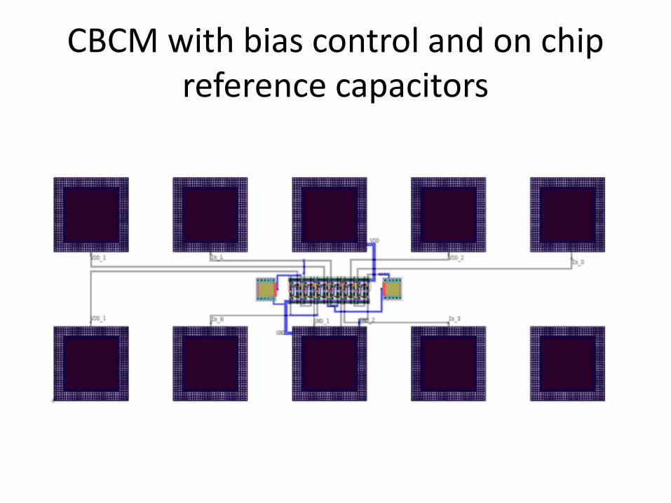
CBCM with bias control and on chip reference capacitors

Interface with AFM • Simulating and testing
proto-type differential current amplifiers.
• Transfer proto-type to miniature circuit board that can clip onto AFM.
• Next chip will integrate differential amplifier and CBCM sensor onto single chip.
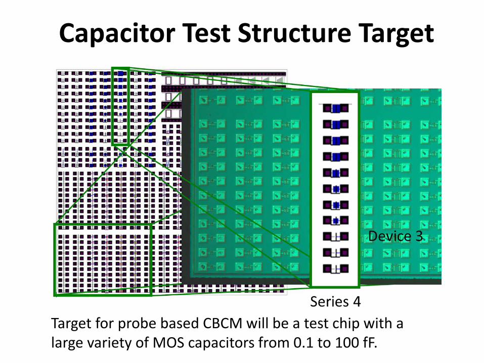
Capacitor Test Structure Target
Target for probe based CBCM will be a test chip with a large variety of MOS capacitors from 0.1 to 100 fF.
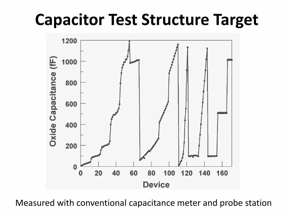
Capacitor Test Structure Target
Measured with conventional capacitance meter and probe station

Acknowledgements