characterization of polysilicon thin films for mems ... · pdf filecharacterization of...
TRANSCRIPT
Characterization of Polysilicon Thin Films for MEMS Applications
DAN O. MACODIYO*1, HITOSHI SOYAMA
2 AND KAZUO HAYASHI
1
1Institute of Fluid Science, Tohoku University, 2-2-1 Katahira, Aoba-ku,
Sendai 980-8577, Japan 2Department of Nanomechanics, Tohoku University, 6-6-01 Aoba, Aramaki,
Aoba-ku, Sendai 980-8579, Japan
Email: [email protected]
Abstract: The microstructure of thin polycrystalline films formed by molecular beam epitaxy (MBE) has been
studied by transmission electron microscopy (TEM). Beneficial compressive residual stress was introduced by
cavitation impacts. Surface morphology was characterized using atomic force microscopy (AFM). The films show
two distinct microstructural regimes at the low and high end with an intermediate transition region.
Homogeneous nucleation and growth in the bulk of the films were observed. Numerous planar twins are
observed on the lower end while the polysilicon films has a highly textured columnar microstructure. The
textured grains had rough edges. Both homogeneous nucleation and growth in the bulk of the films and
heterogeneous nucleation and growth in the film-substrate interface are observed. The main defects have been
identified as dislocations and microtwins. The locations of the dislocations are also discussed.
Keywords: Polysilicon film, Molecular beam epitaxy, Cavitation, Transmission electron microscopy, Defects
1. Introduction
The performance of polysilicon films in micro-
electro-mechanical systems (MEMS) depends on
residual stress and stress gradient, which are adversely
affected by the microstructure. The microstructure is
governed by the properties of the films and the
deposition conditions. Thus, it is necessary to
characterize the microstructure in a bid to meet the
requirements of MEMS systems. Integrated circuit
fabrication technologies requires the definition of small
geometries, precise dimension control, design flexibility,
interfacing with microelectronics, repeatability,
reliability, high yield and low cost. During
microfabrication of semiconductor devices, defects do
occur at micro-scale. These defects may be detrimental
to the performance of device and/or even cause device
failure. The advances in understanding of processes
such as gettering have changed views on impurity
requirements. Defects if properly controlled, can be
used to improve the electrical characteristics of a
silicon-based device [1,2].
When a bubble collapse near another bubble, a wall,
free surface, in a static or dynamic pressure gradient, it
suffers instability that drives the shape to be
nonspherical [3]. The collapsing nonspherical bubbles
develops a microjet which causes plastic deformation
on the wall. The impact of cavitation bubbles, herein
referred to as cavitation impacts, can be used to
generate beneficial residual stress. The authors have
already demonstrated the use of cavitation impacts for
effective gettering of silicon wafers [1,2].
In this study, structural analysis has been performed
using high resolution transmission electron microscopy
(HRTEM). The main defects in the polysilicon films are
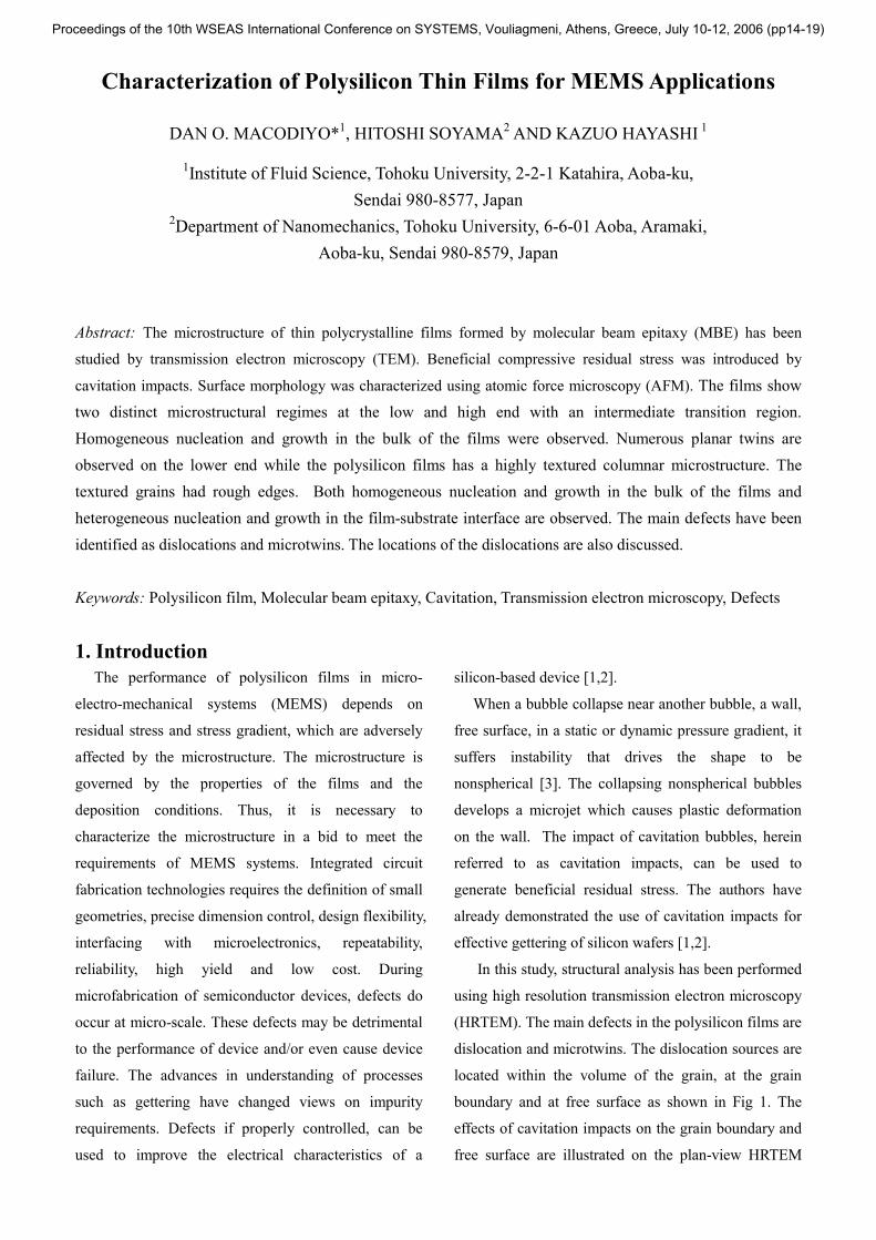
dislocation and microtwins. The dislocation sources are
located within the volume of the grain, at the grain
boundary and at free surface as shown in Fig 1. The
effects of cavitation impacts on the grain boundary and
free surface are illustrated on the plan-view HRTEM
Proceedings of the 10th WSEAS International Conference on SYSTEMS, Vouliagmeni, Athens, Greece, July 10-12, 2006 (pp14-19)

Si2H6
Control valve
Gases
Tray
Wafer
Vacuum pumps
Loading chamber
Heater
Vacuum pumps
have been discussed. The cross-sectional HRTEM view
illustrates fine layer of amorphous and two distinct
microstructural regimes on polysilicon. The growth-
death rate zone at the poly-Si/SiO2 interface highly
which depends on the deposition conditions, had small-
size mixture of textured-columnar crystals. Surface
characterization using the atomic force microscopy
showed that the surface finish on the back of the
polysilicon film was smoothened out by the cavitation
impacts.
Fig. 1 Dislocation sources in polycrystalline silicon
2 EXPERIMENTAL TECHNIQUES
2.1 Sample preparation
2.1.1 Growing polysilicon using a gas-source MBE
Figure 2 shows schematic illustration of the gas-
source molecular beam epitaxy system used for
growing of poly-Si/SiO2 samples. The CZ Si(100)
substrate wafer was chemically cleaned. The sample
was put on the tray and heated to 800 oC for 1 hour to
remove native oxide. Subsequently, a 10 nm silicon
buffer was deposited, followed by heating at 700 oC for
3 hours in disilane (Si2H6) gas at a flow rate of 2.5 sccm.
The pressure during growth was 10-4 Torr.
2.1.2 Introduction of compressive stress
Figure 3 shows the test section of the cavitating jet
apparatus used for the introduction of beneficial
compressive residual stress. The surface of silicon
wafer was masked with a tape and placed onto
specimen holding device and then immersed in DI
water. The test liquid, DI water, was injected onto the
surface of the specimen through a nozzle, diameter 0.8
mm, with an upstream and downstream pressure of 2.5
MPa and 0.1 MPa, respectively. The standoff distance
was 17 mm. The standoff distance sd, is defined as the
distance between the upstream corner of the nozzle
throat and the surface of the specimen under test. Hence,
the optimum standoff distance sopt is determined
qualitatively by an erosion test in which the standoff
distance is varied [4]. Details of the cavitating jet in
submerged condition are found in references [5-9].
Upon leaving the nozzle, a cavitating jet was formed.
The collapsing of the cavitation bubbles causes shock
wave and/or microjets on the specimen surface thereby
causing suitable plastic deformation. The cavitation
impacts was controlled by adjusting hydraulic
parameters such as injection pressure of the cavitating
jet and standoff distance. The cavitating jet was
traversed in the x-direction using an auxiliary leadscrew
controlled by a motor thereby allowing uniform
exposure on the specimen. Thus, the exposure time per
unit length t is expressed as the ratio of the number of
b
Grain
boundaries
Ledge
Dislocation
loop
Grain
Ledge
Grain
Slip
plane
Dislocation
Fig. 2 Schematic illustration of gas-source molecular
beam epitaxy system (AirWater VCE S2020)
Proceedings of the 10th WSEAS International Conference on SYSTEMS, Vouliagmeni, Athens, Greece, July 10-12, 2006 (pp14-19)

scans n to the scanning speed v.
(1)
2.1 Structural characterization
The surface of the specimen treated by cavitation
impact was observed using atomic force microscope.
The threshold deformation and surface roughness of
active device side was 3.99 nm and 2.09 nm,
respectively [10]. In this study, the backside of thin
film was examined.
For the plan-view TEM observation, the specimen
was shaped to 5 mm square using a micro-cutter and
then cleaned using ethyl alcohol (CH3CH2OH). The
sample was fixed to a glass using epoxy resin and
then mechanically polished to thickness t = 20 µm.
The specimen was ion-milled at low angle 12o, 3 kV
and argon flow 0.3 cm3 until perforation. For the
cross-sectional view TEM observations, the samples
were thinned and then glued with deposited films
facing each and the ion-milled. The HTREM
observations were performed using JEOL operated at
300 kV.
3 RESULTS
3.1 Surface characterization of poly-Si/SiO2
using AFM
The surface was characterized using the
Environscope atomic force microscope equipped with
the Nanoscope IV Controller, manufactured by Veeco
(Digital Instruments). Figure 4 shows the AFM images
of the specimen before and after exposing cavitation
impacts. The surface roughness increased due to
cavitation impacts while the deformation on the back-
side of the polysilicon thin film decreased as shown in
Table 1. This shows that the roughness due to
deposition was smoothened out by the cavitation
impacts.
Table 1. Values of surface roughness and deformation
before and after cavitation impacts
Before cavitation
impacts
After cavitation
impacts
Surface
roughness
Ra
Deformation
nm
Surface
roughness
Ra
Deformation
nm
5 610 127 10
3 429 113 37
7 258 153 30
v
nt =
Fig. 3 Test section of cavitation jet apparatus
s
Flow
Overflow Wafer
p
Specimen
holder
Fig. 4 AFM images for surface roughness and
deformation on the back-side of polysilicon film.
(a) Before cavitation impact
(b) After cavitation impact
Proceedings of the 10th WSEAS International Conference on SYSTEMS, Vouliagmeni, Athens, Greece, July 10-12, 2006 (pp14-19)

3.2 Microstructural observation of poly-
Si/SiO2 using HRTEM
Figure 5 shows plan-view HRTEM image indicating
the textured-columnar structure. Parallel microtwins
can be seen along the grain boundary. They are also
associated with dislocation and stacking faults. The slip
planes are evidence where two parallel grains are
inclined. Dislocation sources are also present in ledges.
When the dislocation is at free surface but in the
vertical position an edge dislocation is formed while a
screw dislocation results for the case of horizontal
position of the loop.
Figure 6 shows the cross-sectional bright- and dark
field view of polysilicon film image with g=[220]
reflectance. The microstructure of the polysilicon has
two definite structural sizes. The upper part has large
textural-columnar grains and tends to be near parallel.
The lower part, death-growth zone, has small grains
size 20 to 50 nm. The stacking faults (SF) are illustrated.
The ledge can be seen as a kink between the grain G1
and grain G2. The diffraction pattern around the
microtwins show speckle of bright lights outside the
silicon annular ring with high bright spot in the middle
(see insert in Fig. 6(a)). Half and full dislocation loops
were observed (see Fig. 6(b))
100 nm
Ledge
Parallel microtwins
along the grain
boundary
Fig. 5 Plan-view Poly-Si/SiO2TEM showing
the crystallites
(b) Dark field
Poly-Si SiO2
Si
g
SF SF
Dislocation
loop
Microtwins
Poly-Si SiO2 Si
g
SF
Death-growth
zone
Ledge
G1
G2
(a) Bright field
Fig. 6 Cross-sectional view Poly-Si/SiO2 image with g=[220] reflectance
illustrating stacking faults
Proceedings of the 10th WSEAS International Conference on SYSTEMS, Vouliagmeni, Athens, Greece, July 10-12, 2006 (pp14-19)

4 CONCLUSIONS
The microstructure of polysilicon thin films grown
by MBE and exposed to cavitation impacts has been
studied.
Based on the experimental evidence, the following
conclusions may be drawn:
1. Dislocation sources can be located within the
volume of the grain, at the grain boundary and at
free surface. Dislocation sources located at the
grain boundary generates a dislocation loop. The
size of the dislocation for the specimen treated by
cavitation impacts depends on the grain size and
cavitating parameters. The surface morphology
demonstrates that the rough surface of the as-
deposited gas was smoothened by the cavitation
impact.
2. The films show two distinct microstructural
regimes at the low and high end with an
intermediate transition region. Homogeneous
nucleation and growth in the bulk of the films
were observed. Cavitation impacts decrease the
gap between two intra-grains. Both homogeneous
nucleation and growth in the bulk of the films and
heterogeneous nucleation and growth in the film-
substrate interface are observed. Deformation
streaks and twins were seen on the large columnar
crystals.
3. The death-growth zone at which there is a trade-
off in crystal size is approximately 50 nm in length.
Surface dislocation loops either vertical or
horizontal direction leading to edge and screw-
dislocation were also observed.
Acknowledgments
This work was supported by the Japan Society
for the Promotion of Science (JSPS) under the Grant
No. 16004335. The authors would like to thank Prof.
Noritaka Usami for the assistance on growing
polysilicon films using MBE facility and Mr. Y.
Hayasaka of the IMR, Tohoku University, for his
assistance in TEM observations.
References
1. H. Soyama, S. Saitoh, D. O. Macodiyo and M.
Koyanagi, C-V Characteristics of Backside
Damage Gettering Introduced by a Cavitating Jet in
Silicon Wafer, Proceedings of the 2nd International
Symposium on Mechanical Science based on
Nanotechnology, 2005, pp. 85-88.
2. H. Soyama, S. Saitoh, D. O. Macodiyo, and K.
Hayashi, Evaluation using X-ray diffraction of
backside damage of silicon wafer introduced by a
cavitating jet, Journal of Jet Flow Engineering, Vol.
22, No. 2, 2005, pp 18-22.
3. J.R. Blake and D.C. Gibson, Growth and
Collapse of a Vapor Cavity near a Free Surface.
Journal of Fluid Mechanics, Vol. 111, 1981, pp.
123–140.
4. H. Soyama, Improvement in Fatigue Strength of
Silicon Manganese Steel SUP7 by Using a
Cavitating Jet, JSME International Journal, Vol.
43A, No. 2, 2000, pp. 173 – 178.
5. H. Soyama, T. Kusaka and M. Saka, Peening by the
Use of Cavitation Impacts for the Improvements of
Fatigue Strength, Journal of Material Science
Letter, Vol. 20, 2001, pp. 1263- 1265.
6. H. Soyama, K. Saito and M. Saka, Improvement of
Fatigue Strength of Aluminum Alloy by Cavitation
Shotless Peening, Journal of Engineering
Materials and Technology, Trans. ASME, Vol. 124,
No. 2, 2002, pp. 135 – 139.
7. D. Odhiambo, and H. Soyama, 2003, “Cavitation
Shotless Peening for Improvement of Fatigue
Strength of Carbonised Steel,” International
Journal of Fatigue, Vol. 25, Nos. 9-11, pp. 1217-
1222.
8. D.O. Macodiyo, H. Soyama and M. Saka,
Recrystallization-Etch Observation of Plastic
Deformation Caused by Cavitation Shotless
Peening, Journal of Material Science Letters, Vol.
22, No. 2, 2003, pp. 115-117.
9. D.O. Macodiyo and H. Soyama, Optimization of
Cavitation Peening Parameters for Fatigue
Performance of Carburized Steel Using Taguchi
Methods, Journal of Materials Processing
Technology, 2006, in press.
10. D.O. Macodiyo, H. Soyama and K. Hayashi,
Characterization of Defects for Effective Gettering
Proceedings of the 10th WSEAS International Conference on SYSTEMS, Vouliagmeni, Athens, Greece, July 10-12, 2006 (pp14-19)

in Silicon Wafer and Polysilicon Thin Films,
Proceedings of the 8th Biennial ASME Conference
on Engineering Systems Design and Analysis, July
4-7, 2006, ( to be published).
Proceedings of the 10th WSEAS International Conference on SYSTEMS, Vouliagmeni, Athens, Greece, July 10-12, 2006 (pp14-19)