characterization of organic contaminants outgassed · pdf file3/25/03 p. sun/c. ayre, ca...
TRANSCRIPT

3/25/03 P. Sun/C. Ayre, CA MATTEC, Intel 1
Characterization of Organic Contaminants Outgassed from Materials Used in Semiconductor Fabs/Processing
Peng Sun and Caroline Ayre California Materials Technology
Intel Corporation

3/25/03 P. Sun/C. Ayre, CA MATTEC, Intel 2
Outline
• Introduction• Analytical Methods for Materials’ Outgassing
Measurements• Characterization of Outgassed Organic Contaminants
Using Thermal Desorption-Gas Chromatography-Mass Spectrometry (TD-GC-MS)
• Ammonia/Amines’ Outgassing• Summary
3/25/03 P. Sun/C. Ayre, CA MATTEC, Intel 3
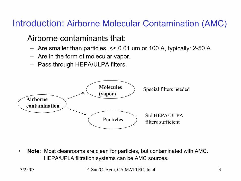
Introduction: Airborne Molecular Contamination (AMC)Airborne contaminants that:– Are smaller than particles, << 0.01 um or 100 Å, typically: 2-50 Å. – Are in the form of molecular vapor. – Pass through HEPA/ULPA filters.
• Note: Most cleanrooms are clean for particles, but contaminated with AMC.HEPA/UPLA filtration systems can be AMC sources.
Airborne contamination
Molecules(vapor)
Particles
Special filters needed
Std HEPA/ULPA filters sufficient

3/25/03 P. Sun/C. Ayre, CA MATTEC, Intel 4
Introduction: Airborne Molecular Contamination (AMC)
• AMC Classification (SEMI F21-95):– Acids: HCl, HF, HNO3, H2SO4– Bases: NH3, amines, NMP– Condensables: organics with boiling point (bp) > 150 oC– Dopants: P, B, As compounds
• Material outgassing is one of the major sources of AMC.
• Notes:1. Some compounds belong to more than one class.2. Some compounds are not covered by this classification.3. NMP: N-methyl-pyrrolidinone, photoresist stripper or polyimide solvent.

3/25/03 P. Sun/C. Ayre, CA MATTEC, Intel 5
Introduction: Molecular Condensables (MC)• Known Problematic Organic Contaminants:
– Flame retardants, e.g. organophosphorus – Siloxanes– Polymer/plastic additives, e.g. plasticizers, antioxidants– Amines/amides (such as NMP) – Decomposition compounds
• Effects of Organic Contamination:– Surface properties (e.g. hydrophobicity)– Lower breakdown voltage – Unintentional doping– Haze degradation– Oxide growth rate and quality – Post-CVD defects– Delamination– Optic and mask hazing

3/25/03 P. Sun/C. Ayre, CA MATTEC, Intel 6
Introduction: Effects of Organic Contamination -Unintentional Doping Due to Outgassing
• Unintentional doping on Si device wafers during furnace operation was observed.• Witness wafer test showed that phosphorus contamination on witness wafers was roughly linear
with exposure time.• TD-GCMS analysis of various components of HEPA filters identified that the contaminant as Fyro
PCF flame retardant outgassed from the HEPA polyurethane potting material.
Reference: J.A. Lebens, et al., “Unintentional doping of wafers due to organophosphates in the cleanroom ambient”, J. Electrochem. Soc., 143(9), 2906-2909 (1996).
Sheet resistance map of a contaminated waferPhosphorus contamination vs. exposure time of witness wafer to cleanroom contaminated by Fyrol

3/25/03 P. Sun/C. Ayre, CA MATTEC, Intel 7
Introduction: Effects of Organic Contamination -Breakdown Voltage Reduction
• Notes: 1. Organic contamination on the first SiO2 surface causes degradation in the polysilicon layer, resulting in breakdown field strength reduction. 2. Storage time in cassettes prior to the first polysilicon deposition can affect breakdown field strength.
Reference: M. Tamaoki, et al., “The effect of airborne contaminants in the cleanroom for ULSI manufacturing process”, 1995 IEEE/SEMI Advance Semiconductor Manufacturing Conference, 322-326 (1995).
Wafers exposed to cleanroom w/o chemical filters
Wafers exposed to cleanroom with chemical filters
Device structure used to measure breakdown strength of inter-polysilicon SiO2

3/25/03 P. Sun/C. Ayre, CA MATTEC, Intel 8
Introduction: Sources of Organic Outgassing Contamination
– sealants – adhesives – paints – lubricants – plastics– HEPA/ULPA filtration systems – floor tiles – wafer carriers – cleanroom consumables: gloves, garments, tapes, cleaners… – process chemicals– people …

3/25/03 P. Sun/C. Ayre, CA MATTEC, Intel 9
Introduction: ITRS Roadmap for Wafer Surface Organics
Wafer surface organic contamination: Carbon atoms/cm2:
2001 2002 2003 2004 2005 2006 2007Technology (nm): 130 90 65
‘99 edition: 6.6x10¹³ 5.3x10¹³ 4.9x10¹³ 4.5x10¹³ 4.1x10¹³ 2.1x10¹³ (2008)
‘02 edition: 2.6x10¹⁴ 2.1x10¹³ 1.8x10¹³ 1.5x10¹³ 1.3x10¹³ 1.1x10¹³ 1.0x10¹³
• Trend: Tighter wafer surface organic contamination requirements due to increasing sensitivity to organic condensables’ contamination.

3/25/03 P. Sun/C. Ayre, CA MATTEC, Intel 10
Outline
• Introduction• Analytical Methods for Materials’ Outgassing
Measurements• Characterization of Outgassed Organic Contaminants
Using Thermal Desorption-Gas Chromatography-Mass Spectrometry (TD-GC-MS)
• Ammonia/Amines’ Outgassing• Summary

3/25/03 P. Sun/C. Ayre, CA MATTEC, Intel 11
Analytical Methods for Outgassing Measurements
• Most widely used methods in semiconductor industry:– Direct Outgassing
• Weight loss method– for total outgassing assessment
• TD-GC-MS method– for outgassing compound identification and quantification
– Indirect Outgassing Measurement Using Witness Wafers• TD-GC-MS analysis of witness wafers
– full wafer analysis• Time-of-flight Secondary Ion Mass Spectrometry (TOF-SIMS)
analysis of witness wafers– spot analysis

3/25/03 P. Sun/C. Ayre, CA MATTEC, Intel 12
Analytical Methods for Outgassing Measurements
• Industry Standards:– ASTM F1227-89, “Standard Test Method for Total Mass Loss of
Materials and Condensation of Outgassed Volatiles on Microelectronics-Related Substrates”
– IEST WG-CC031 Recommended Practice: “Method for Characterizing Outgassed Organic Compounds from Cleanroom Materials and Components” (to be published in 2003)
– SEMI Environmental Contamination Control (ECC) WG: SEMI E108-0301: “Test Method for The Assessment of Outgassing Organic Contamination from Minienvironments Using Gas Chromatography/Mass Spectroscopy”
– ASTM F1982-99: “Standard Test Methods for Analyzing Organic Contaminants on Silicon Wafer Surfaces by Thermal Desorption Gas Chromatography”

3/25/03 P. Sun/C. Ayre, CA MATTEC, Intel 13
Outline
• Introduction• Analytical Methods for Materials’ Outgassing
Measurements• Characterization of Outgassed Organic Contaminants
Using Thermal Desorption-Gas Chromatography-Mass Spectrometry (TD-GC-MS)
• Ammonia/Amines’ Outgassing• Summary

3/25/03 P. Sun/C. Ayre, CA MATTEC, Intel 14
Characterization of Outgassed Organic Contaminants Using TD-GC-MS
• Schematic Diagram of TD-GC-MS Technique:

3/25/03 P. Sun/C. Ayre, CA MATTEC, Intel 15
Detection of Outgassed Polycyclodimethyl-siloxanes from a Cleanroom Sealant
• TD-GC-MS Analysis Results:
Total outgassing: 680 ug/g
Siloxanes: 290 ug/g
Total organics: 7.6 ng/cm2
Siloxanes: 6 ng/cm2
Direct outgassing of a sealant
Surface analysis of a witness wafer exposed to the sealant:
Siloxane: 2.5E14 Carbon atoms/cm2, 10x > ITRS requirement (1.8E13)
ug = microgram, ng = nanogramRetention Time (min)
3/25/03 P. Sun/C. Ayre, CA MATTEC, Intel 16
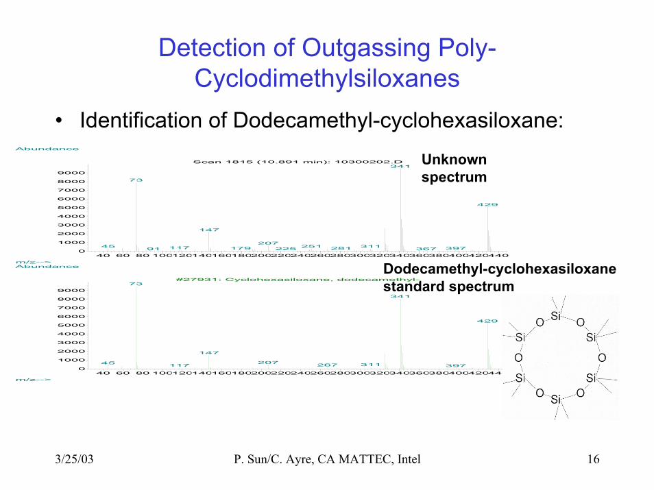
Detection of Outgassing Poly-Cyclodimethylsiloxanes
• Identification of Dodecamethyl-cyclohexasiloxane: Unknown spectrum
Dodecamethyl-cyclohexasiloxane standard spectrum
40 60 80 1001201401601802002202402602803003203403603804004204400
1000
2000
3000
4000
5000
6000
7000
8000
9000
m/z-->
Abundance
Scan 1815 (10.891 min): 10300202.D341
73
429
147
20745 251 311117 179 39728122591 367
40 60 80 1001201401601802002202402602803003203403603804004204400
1000
2000
3000
4000
5000
6000
7000
8000
9000
m/z-->
Abundance
#27931: Cyclohexasiloxane, dodecamethyl-73
341
429
147
20745 311267117 397

3/25/03 P. Sun/C. Ayre, CA MATTEC, Intel 17
Detection of Triethyl Phosphate (TEP) Outgassed from a Cleanroom Sealant
Triethyl phosphate: 49 ug/g
Triethyl phosphate: 5.8 ng/cm2
5.00 10.00 15.00 20.00 25.00 30.00 35.00
1000000
2000000
3000000
4000000
5000000
6000000
7000000
8000000
9000000
1e+07
1.1e+07
1.2e+07
1.3e+07
1.4e+07
Time-->
Abundance
TIC: 12160202.D
5.00 10.00 15.00 20.00 25.00 30.00 35.00
500000
1000000
1500000
2000000
2500000
3000000
3500000
4000000
4500000
5000000
5500000
6000000
6500000
7000000
7500000
8000000
8500000
9000000
9500000
Time-->
Abundance
TIC: 12060206.D
Direct outgassing of a cleanroom sealant
Surface analysis of witness wafer exposed to the same sealant
~2E13 P atoms/cm2, >> critical level: 1E12
Retention Time (min)

3/25/03 P. Sun/C. Ayre, CA MATTEC, Intel 18
Detection of Triethyl Phosphate (TEP) Outgassed from a Cleanroom Sealant
• Identification of Triethyl phosphate (TEP):
Triethyl phosphate standard spectrum
Unknown spectrum
20 40 60 80 100 120 140 160 180 200 220 240 260 2800
2000
4000
6000
8000
m/z-->
Abundance
Scan 1929 (11.563 min): 12160202.D155
99
127
81
111 13945 18265 167 207 235 263 29133
20 40 60 80 100 120 140 160 180 200 220 240 260 2800
2000
4000
6000
8000
m/z-->
Abundance
#43455: Triethyl phosphate99
155
12781
29
45 1111396515 182167

3/25/03 P. Sun/C. Ayre, CA MATTEC, Intel 19
Characterization of Outgassed Organic Contaminants Using TD-GC-MS
• Polymer materials chosen outgas organic contaminants commonly seen in semiconductor Fab cleanrooms. Organic contaminants monitored included:
• polycyclodimethylsilocxanes• Dibutyl phthalate (DBP)• Butylated hydroxytoluene (BHT)• 2-Ethyl-1-hexanol• Methylstyrene• Naphthalene
• Outgassing behaviors of selected contaminants were studied by varying the following parameters:
• outgassing time• outgassing temperature• surface area• weight

3/25/03 P. Sun/C. Ayre, CA MATTEC, Intel 20
Outgassing Concentration vs. Outgassing Time: Siloxanes
• Linear relationship between outgassing concentration and outgassing time within a time range. Outgassing rate can be estimated from the slope.
• Same findings for Dibutyl phthalate (DBP) and Butylated hydroxytoluene (BHT)(not shown).
• Linear relationship was also observed at 75 oC with higher slope values, indicating higher outgassing rate at 75 oC.
Outgassing Time Dependance (at 50oC)
y = 0.0236x + 0.0744R2 = 0.9993
y = 0.0394x + 0.0609R2 = 0.9872
y = 0.0358x + 0.2154R2 = 0.9816
0.00
0.20
0.40
0.60
0.80
1.00
1.20
0 5 10 15 20 25 30 35Outgassing Time (min)
Out
gass
ing
Con
cent
ratio
n (p
pmw
, ng/
g)
Octamethyl-cyclotetrasiloxane
Decamethyl-cyclopentasiloxane
Dodecamethyl-cyclohexasiloxane

3/25/03 P. Sun/C. Ayre, CA MATTEC, Intel 21
Outgassing Concentration vs. Temperature: Siloxanes and DBP
• Linear relationship between Log (Outgassing Conc.) and inverse of outgassing temperature (1/T).
• In agreement with findings reported by K. Takeda, et al., IEST 2000 ESTECH Proceedings, pp. 71-77 (2000).
• Same result was observed for Butylated hydroxytoluene (BHT) (not shown).
Outgassing vs. Temperature
y = -3.9015x + 11.825R2 = 0.9726
y = -1.724x + 5.301R2 = 0.9945
y = -1.782x + 5.4216R2 = 0.9977
y = -1.5764x + 4.6101R2 = 0.9841
-1.00
-0.50
0.00
0.50
1.00
1.50
2.00
2.50
2.50 2.60 2.70 2.80 2.90 3.00 3.10 3.20
1/T x 103 (1/K x 103)
Log
(Out
gass
ing
Con
c.)
Octamethyl-cyclotetrasiloxaneDecamethyl-cyclopentasiloxaneDodecamethyl-cyclohexasiloxaneDibutyl Phthalate (DBP)

3/25/03 P. Sun/C. Ayre, CA MATTEC, Intel 22
Outgassing Quantity vs. Surface Area: Siloxanes
• Outgassing quantity ∝ surface area when sample weight is constant.
Siloxane Outgassing Dependence on Sample Surface Area (outgassing condition: 50oC, 15 min)
0
100
200
300
400
500
600
700
Octamethyl-cyclotetrasiloxane
Decamethyl-cyclopentasiloxane
Tetradecamethyl-cycloheptasiloxane
Outgassing Compound
Tota
l Out
gass
ing
(ng)
1x surface area, 1x sample weight
2x surface area, 1x sample weight
Outgassing ∝ Surface Area
1x surface area 1x weight
2x surface area 1x weight

3/25/03 P. Sun/C. Ayre, CA MATTEC, Intel 23
Outgassing Quantity vs. Sample Surface Area
• Outgassing quantity ∝ surface area when sample weight is constant.1x surface area 1x weight
2x surface area 1x weight
Outgassing Dependence on Sample Surface Area (outgassing condition: 50oC, 15 min)
0
100
200
300
400
500
600
2-ethyl-1-hexanol Methylstyrene Naphthalene
Outgassing Compound
Tota
l Out
gass
ing
(ng)
1x surface area, 1x sample weight
2x surface area, 1x sample weight
Outgassing ∝ Surface Area

3/25/03 P. Sun/C. Ayre, CA MATTEC, Intel 24
Outgassing Quantity vs. Sample WeightOutgassing Dependence on Sample Weight (50oC, 15min)
0
100
200
300
400
500
600
Octamethyl-cyclotetrasiloxane
Decamethyl-cyclopentasiloxane
Tetradecamethyl-cycloheptasiloxane
Outgassing Compound
Tota
l Out
gass
ing
(ng)
1x sample weight, 1x surface area
2x sample weight, 1x surface area
Outgassing is independent of sample weight
• Outgassing is independent of sample weight when surface area is constant.• Same results for methylstyrene, 2-ethyl-1-hexanol and naphthalene (not shown).

3/25/03 P. Sun/C. Ayre, CA MATTEC, Intel 25
Conclusions: Characterization of Outgassed Organic Contaminants Using TD-GC-MS
• Linear relationship between outgassing concentration and outgassing time in a certain time range.– where the slope equals the outgassing rate.
• Linear relationship between logarithm of outgassing concentration and 1/T; where ‘T’ is the absolute outgassing temperature.
• Outgassing amount ∝ sample surface area.• Outgassing is independent of sample weight when surface area
remains constant.– Suggests that outgassing is indeed a surface phenomenon.
Note: These findings are based on the limited number of contaminantstested.
– Materials’ outgassing can be far more complicated due to large number of variables in the physical and chemical properties of different materials used in cleanrooms.

3/25/03 P. Sun/C. Ayre, CA MATTEC, Intel 26
Outline
• Introduction• Analytical Methods for Materials’ Outgassing
Measurements• Characterization of Outgassed Organic Contaminants
Using Thermal Desorption-Gas Chromatography-Mass Spectrometry (TD-GC-MS)
• Ammonia/Amines’ Outgassing• Summary
3/25/03 P. Sun/C. Ayre, CA MATTEC, Intel 27
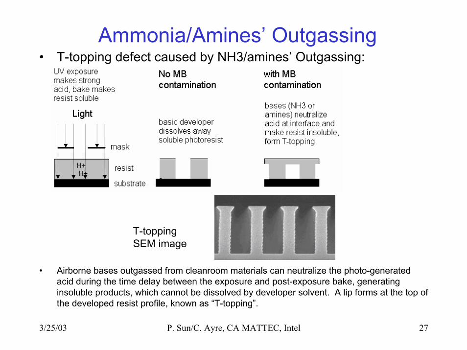
Ammonia/Amines’ Outgassing• T-topping defect caused by NH3/amines’ Outgassing:
• Airborne bases outgassed from cleanroom materials can neutralize the photo-generated acid during the time delay between the exposure and post-exposure bake, generating insoluble products, which cannot be dissolved by developer solvent. A lip forms at the top of the developed resist profile, known as “T-topping”.
T-topping SEM image

3/25/03 P. Sun/C. Ayre, CA MATTEC, Intel 28
Ammonia/Amines’ Outgassing• Gas Diffusion-Conductivity Detection-based
NH3/Amines’ Outgassing Method:
ppb = parts per billion
Capable of detecting 1 ng/g (ppb) of NH3/amines’ outgassed
3/25/03 P. Sun/C. Ayre, CA MATTEC, Intel 29
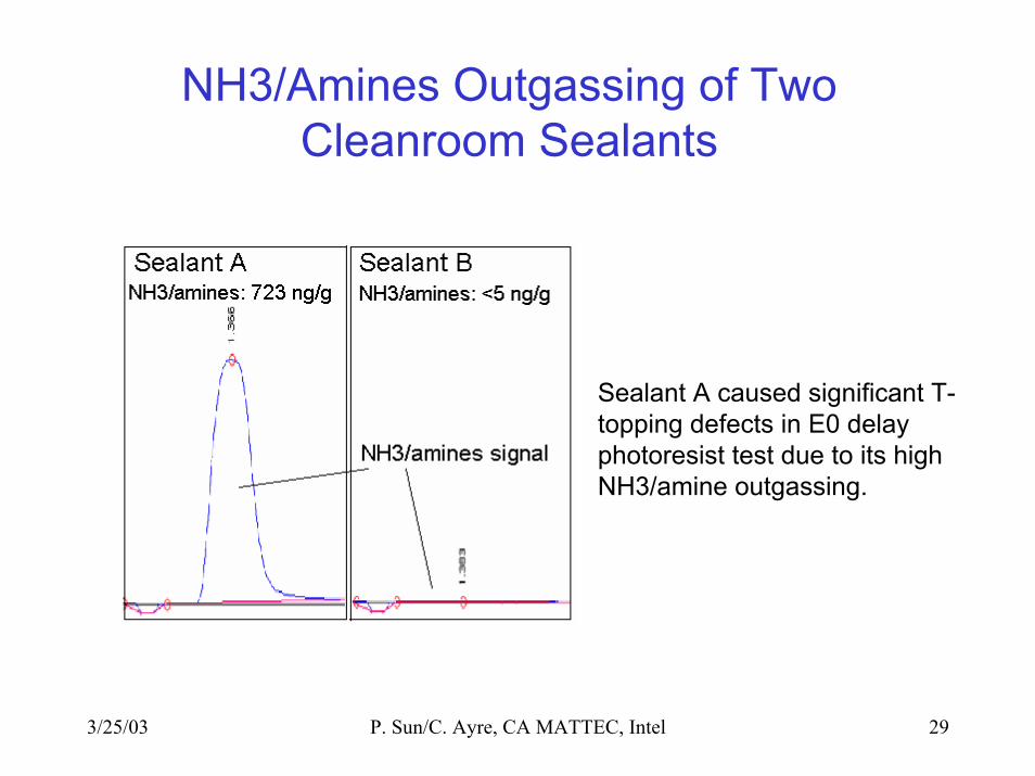
NH3/Amines Outgassing of Two Cleanroom Sealants
Sealant A caused significant T-topping defects in E0 delay photoresist test due to its high NH3/amine outgassing.

3/25/03 P. Sun/C. Ayre, CA MATTEC, Intel 30
Time Dependence of NH3/Amines’ Outgassing
Time dependent NH3/amine outgassing of a sealant: room temperature
Surface NH4+ of witness wafers exposed to same sealant: room temperature
NH3/Amine Outgassing vs. Cure Time
0100200300400500600700800
0 10 20 30 40 50 60 70 80
Cure Time (hour)
NH3/
Amin
e O
utga
ssin
g (n
g/g)
Wafer Surface NH4+ vs. Cure Time(1 hour exposure at room temperature)
0
500
1000
1500
2000
2500
3000
0 10 20 30 40 50 60 70 80Cure Time (hour)
Waf
er S
urfa
ce N
H4+
(E10
NH4
+/cm
2)
control wafer

3/25/03 P. Sun/C. Ayre, CA MATTEC, Intel 31
NH3/Amines’ Outgassing vs. Wafer Surface NH4+
Wafer Exposure Test(1 hour exposure at room temperature)
0
500
1000
1500
2000
2500
3000
0 100 200 300 400 500 600 700 800NH3 Outgassing
(ng/g)
Waf
er S
urfa
ce N
H4+
(E
10 N
H4+
/cm
2)
Linear relationship between witness wafer surface NH4+ and sealant NH3/amines’ outgassing concentration

3/25/03 P. Sun/C. Ayre, CA MATTEC, Intel 32
Summary• Many AMC contaminants found in semiconductor Fabs come
from outgassing of cleanroom materials. Outgassed contaminants can adversely affect many processes, resulting in yield loss, shortened tool life and reduced long-term device reliability.
• The large variety of cleanroom materials and numerous outgassing contaminants combined with the complexity of process steps makes understanding detrimental levels of specificcontaminants in particular processes very challenging.
• Screening materials for both condensable and NH3/amines’ outgassing prior to bringing them into Fabs can be used as a first-line-of-defense against molecular contaminants such asorganophosphorus, siloxanes, plasticizers and ammonia/amines.

3/25/03 P. Sun/C. Ayre, CA MATTEC, Intel 33
Summary
• New microelectronic fabrication processes with decreasing device geometries are increasingly susceptible to AMC.
• As processes and chemistries change, requirements for monitoring, control and analysis of materials’ outgassing will evolve as well.
• Cooperative efforts among manufacturers of integrated circuit, materials and analytical tools are needed to better understand the impact of molecular contaminants and to properly define specifications applicable to new ULSI technologies.

3/25/03 P. Sun/C. Ayre, CA MATTEC, Intel 34
Acknowledgements
• Yaacov Maoz of Intel Fab 18 for providing the “T-topping” defect SEM image.
• Zari Pourmotamed of Intel California Materials Technology for collecting time-dependent NH3/amines’ outgassing data.
• Joseph O’Sullivan of Intel Facilities Technology for providing valuable technical inputs.