characterization of iron oxide thin films for
TRANSCRIPT

UNLV Theses, Dissertations, Professional Papers, and Capstones
2009
Characterization of iron oxide thin films for photoelectrochemical Characterization of iron oxide thin films for photoelectrochemical
hydrogen production hydrogen production
Kyle Eustace Nelson George University of Nevada Las Vegas
Follow this and additional works at: https://digitalscholarship.unlv.edu/thesesdissertations
Part of the Oil, Gas, and Energy Commons, and the Physical Chemistry Commons
Repository Citation Repository Citation George, Kyle Eustace Nelson, "Characterization of iron oxide thin films for photoelectrochemical hydrogen production" (2009). UNLV Theses, Dissertations, Professional Papers, and Capstones. 147. http://dx.doi.org/10.34917/1391032
This Thesis is protected by copyright and/or related rights. It has been brought to you by Digital Scholarship@UNLV with permission from the rights-holder(s). You are free to use this Thesis in any way that is permitted by the copyright and related rights legislation that applies to your use. For other uses you need to obtain permission from the rights-holder(s) directly, unless additional rights are indicated by a Creative Commons license in the record and/or on the work itself. This Thesis has been accepted for inclusion in UNLV Theses, Dissertations, Professional Papers, and Capstones by an authorized administrator of Digital Scholarship@UNLV. For more information, please contact [email protected].

CHARACTERIZATION OF Fe2O3 THIN FILMS FOR PHOTOELECTROCHEMICAL HYDROGEN PRODUCTION
by Nelson George of Arts ada, Las Vegas 8
ts for the
e in Chemistry Degree Department of Chemistry
College of Sciences
Graduate College University of Nevada, Las Vegas
December 2009
Kyle Eustace cheloBa rU rsity of Nev200nive
in partial fulfillmentemenA thesi submittedof the requirs
Master f Scienco
ii
THE GRADUATE COLLEGE
prepared under our supervision by
entitled
Characterization of Fe2O3 Thin Films for Photoelectrochemical
for the degree of
cience Chemistry
ee Chair
e Member
ber
Ronald Smith, Ph. D., Vice President for Research and Graduate Studies
of the Graduate College December 2009
We recommend that the thesis
Kyle Eustace Nelson George
Hydrogen Production
be accepted in partial fulfillment of the requirements
ster of SMa
Clemens Heske, Committ David Hatchett, Committe Dong-Chan Lee, Committee Mem
James Selser, Graduate Faculty Representative
and Dean
iii
ABSTRACT Characterization of Fe2O3 Thin Films for Photoelectrochemical
rogen Production by e Nelson George D ination Committee Chair al Chemistry s Vegas ble. However, solar olution to weaning g solar energy are promising option – h hydrogen being ly clean nature. A ces hydrogen by tilizing “free” solar
applications with a lly believed to be its use as a water of hematite implies pite this, α-Fe2O3 is cheap and abundant, nontoxic and easily synthesized. Furthermore, several studies have shown that this material is particularly receptive to both n- and p-type doping
Hyd
K le Eustacyr. Clemens Heske, ExamProfessor of Materials/Physic, LaUniversity of NevadaSolar energy is the most sustainable source of energy availaapplications such as photovoltaic cells represent only a partial sour dependence upon fossil fuels. Several methods of storincurrently being pursued, and chemical storage stands out as acombining design simplicity with high energy density, witparticularly attractive because of its abundance and inherentmonolithic Photoelectrochemical (PEC) device that produelectrolyzing water directly from sunlight has the benefit of uenergy to drive the reaction. Although α-Fe2O3 (hematite) is a strong candidate for PEC bandgap of 2.2 eV, its conduction band minimum is generapositioned below the H+/H2 reduction potential necessary forsplitting material. Additionally, the low charge carrier mobilitythat charge carrier recombination needs to be overcome. Des

– a solution that may address both the band edge position and charge mobility issues. XPS) conducted at ed by Dr. Asanga characterization by of California, Santa les grown by our . Eric McFarland at tions of Ti diffusion owth due to high s incorporated into rmance.
This thesis describes X-ray Photoelectron Spectroscopy (F rUNLV, Atomic orce Microscopy (AFM) imaging perfo mRanasinghe (also UNLV), Scanning Electron Microscopy (SEM)Arnold Forman and Alan Kleiman-Shwarsctein at the UniversityBarbara (UCSB), and the synthesis process of α-Fe2O3 sampcollaborators Arnold Forman, Alan Kleiman-Shwarsctein, and DrUCSB. We describe the synthesis process and report our observathrough the Ti/Pt substrate interface and of Fe2O3 island grcalcination temperatures. Furthermore, we identify contaminant with PEC sample perfothe samples, and correlate these findings
vi

v
ACKNOWLEDGEMENTS Although thesis writing is formally an individual activity, this work would not be possible were it no pport I have had from advisors, colleagues, e unable to produce ond this. Professor , you have given me ath that has brought thusiasm and good e, but as a student, I accessible. I truly n over the years. ou over the years, I strongly associate ur ability to speak tectiveness of those of my appreciation ally, professionally -class research that pened the door to graduate school, and allowed me to arrive at the decision to walk through it – forever changing my life’s path. More importantly, your council has helped me
t for the amazing sufriends, and family along the way. To my thesis committee: in the most literal sense I would bthis document without you, however my gratitude goes far beyJames Selser, by giving me a strong foundation in basic physicsthe tools to explore science and the world, leading me down a pus to this point. Professor Dong-Chan Lee, in academia your ennature may be less important than the extent of your knowledgbelieve your approachability has made your knowledge moreappreciate your feedback, advice and general conversatioProfessor David Hatchett, having taken several classes with yinviting you to serve on my committee was an easy decision, formy self-identity as a chemist with your training. I admire yodirectly when the situation so requires, and I respect your proaround you. Professor Clemens Heske, I cannot fully express the depthfor your mentorship and guidance through the years –academicand personally. As an undergraduate, you involved me in worldmany scientists can only dream of having access to. You o

vi
through the toughest points in my personal life; supporting me when I needed support, encouraging me when I needed encouragement, and listening when I respect, admiration f the University of s and support that sis. His graduate ent countless hours assing thanks. You te your sacrifice of friendship that has earch Group, your plete not only my ave I been part of a r fellow colleagues. f my workload so I ot go unnoticed, or through our group eir knowledge and Zhang, Dr. Ich Tran, Dr. Asanga Ranasinghe, and Dr. Stefan Krause, I admire your expertise and strive to attain your level. I extend special thanks to Dr. Zhang for reviewing my early drafts,
needed an ear. It is this personal attention that has won you theand devotion of your research group. I also owe sincere thanks to Professor Eric McFarland oCalifornia, Santa Barbara for providing the samples, resourceallowed me to conduct the research that developed into this thestudents Arnold Forman and Alan Kleiman-Shwarsctein have spassisting me throughout this process, and deserve more than phave been gracious and accommodating hosts, and I appreciaweekends and late nights and too-early mornings. I value the grown over the course of our working relationship. To my friends and colleagues in Professor Heske’s Ressupport through my ups and downs has allowed me to comundergraduate degree, but my Master of Science degree. Never hworking environment with such complete and total support foAt times of great personal trials, you have shouldered some ocould focus on these issues, and this willingness to help out did nunappreciated. The post-doctoral scholars who have passed have set the standard for excellence by the breadth of thexperience. Dr. Lothar Weinhardt, Dr. Marcus Bär, Dr. Yufeng

vii
to Dr. Ranasinghe for the AFM imaging that helped me better understand my data. I especially thank Dr. Krause for being my coffee partner, for spending hours nd for reining me in fmann, and Sujitra ent develops into a gh the road may be rt and help. Thanks ug Hanks, Graham ire academic career, d in myself, and for Marjorie Reyes, and education above all gside me when I t all. Thank you for for your love; and ackenzie Elizabeth ou all the time and ays forgave me, and that means the world to me. Your daddy loves you more than you will ever know, and I work every day hoping to become the role model you can look up to.
discussing my experimental design over many cups of coffee, awhen my plans exceeded my schedule and capabilities. To my fellow graduate students, Moni Blum, Timo HoPookpanratana, who have shown me how a raw graduate studPh.D. Watching you blaze the trail has shown me that althoulong, it is certainly surmountable. Thank you for all your suppoalso go out to the undergraduates in our research group, DoHaugh, Fatima Khan, and Bhakthi Amarasinghe. To my friends who have supported me throughout my entyou have sometimes had more confidence in me than I have hathis I thank you. And finally, I dedicate my thesis to my family. To my mom, to my dad, Nelson George, both of whom have always placed else. To my own new family: Dr. Sarah Johnson, who sacrificed alonchose to return to academia, and stood by my side throughout ihaving the faith in me that allows me to keep going; thank youthank you for the greatest gift in my life. To our daughter, MGeorge, you may not have understood why daddy did not give yattention you deserved over the last few months, yet you alw

viii
TABLE OF CONTENTS ABSTRACT .................................................................................................................................................... iii ACKNOWLEDGEMEN ........................................................................................... v ........................................ x ..................................... xii ....................................... 1 ....................................... 1 ....................................... 1 ....................................... 4 ....................................... 6 ....................................... 6 ....................................... 7 ..................................... 11 ..................................... 11 ..................................... 11 ..................................... 12 ..................................... 13 ..................................... 16 ..................................... 16 ..................................... 18 ..................................... 19 ..................................... 19 ..................................... 20 ..................................... 23 ..................................... 25 ..................................... 25 ..................................... 30 ..................................... 35 ..................................... 35 ..................................... 48 ..................................... 51 55 ..................................... 57 ..................................... 59 5.6.1 Quantification of Composition ................................................................................ 59 5.6.2 Oxide Formation ............................................................................................................ 62 5.6.3 Film Thickness & Morphology ................................................................................. 64
TS ................................ LIST OF FIGURES ................................................................................................. LIST OF ABBREVIATIONS ............................................................................... CHAPTER 1 INTRODUCTION .........................................................................1.1 Background and Motivation ......................................................1.1.1 Solar Energy ............................................................................. 1.1.2 Hydrogen ...................................................................................CHAPTER 2 PHOTOELECTROCHEMICAL WATER SPLITTING .......2.1 Background and Motivation ......................................................2.1.1 Fe2O3 Photoanodes ............................................................... CHAPTER 3 EXPERIMENTAL TECHNIQUES & INSTRUMENTS ......1 3. X-ray Photoelectron Spectroscopy .........................................1.1.1 Photoelectron Spectroscopy Overview ........................1.1.2 Inelastic Mean Free Path ....................................................1.1.3 Heske Group’s XPS Capabilities .......................................3.2 Incident Photon-to-Current Efficiency .................................3.3 Atomic Force Microscopy ...........................................................3.4 Scanning Electron Microscopy ................................................. CHAPTER 4 α-Fe2O3 Sample Films ..............................................................4.1 Introduction ......................................................................................4.2 Synthesis .............................................................................................4.3 Experimentation ............................................................................. CHAPTER 5 RESULTS AND DISCUSSION ..................................................5.1 Sample and Experimental Quality Control ...........................5.2 Sample Spectra Overview ............................................................5.3 Sample Preparation Findings .....................................................5.3.1 Effect of Calcination on Morphology ...............................5.3.2 Activity of Fe Due to Calcination .......................................5.3.3 Sample Contamination ..........................................................5.4 Furnace 1 and Furnace 2 Sample Differences .......................................................... 5.5 The “Mystery Sample” ...................................................................5.6 Discussion ...........................................................................................

ix
5.6.4 Carbon ................................................................................................................................ 65 CHAPTER 6 SUMMARY AND FUTURE WORK ............................................................................. 70 ..................................... 70 ..................................... 71 ..................................... 74 77 6.1 Summary ..............................................................................................6.2 Future work ........................................................................................ BIBLIOGRAPHY .................................................................................................... VITA ...............................................................................................................................................................

x
LIST OF FIGURES Figure 1.1: Standard Solar Spectra for space and terrestrial use. .................................. 3 Figure 2.1: Diagram electrochemical Cell. .................................................. 7 Figure 3.1: The Uni IMFP in solids............................................................... 12 ..................................... 14 ..................................... 15 .................................... 17 ..................................... 22 ..................................... 23 ..................................... 25 e eam-induced ..................................... 26 onitor possible xposure ................... 27 ace .............................. 29 ..................................... 30 31 and 400 nm Fe ..................................... 32 33 ..................................... 35 ed .............................. 36 Fe film ...................... 37 Fe film ................... 38 O3 film ..................... 39 ..................................... 40 f a May 2009 0 ..................................... 41 the emergence urface already ..................................... 43 annealing, after ..................................... 44 EC film (cross ..................................... 45 p view) .................... 46 ................................... 46 tion) .......................... 47 ..................................... 48 ..................................... 49 mples ......................... 49 samples................ 50 Figure 5.26: Sample positions during calcination .................................................................. 51 Figure 5.27: XPS spectra of the Al 2s region of Pt samples ................................................ 52 Figure 5.28: XPS spectra of the Al 2s region for December 2008 samples .................. 53
of Fe2O3 Photoversal C rve of uFigure 3.2: Schematic diagram of the XPS experimental setup.Figure 3.3: Monochromator operating principle ............................Figure 3.4: Simplified diagram of an Atomic Force MicroscopeFigure 4.1: N2 glovebag sample extraction setup ............................Figure 4.2: Furnace 1 glovebag setup ................................................. bFigure 5.1: XPS spectrum of a reference Pt foil .................................Figur 5.2: Series of O 1s XPS spectra to monitor possible........damage during a 4-hour radiation exposure .... o /2 o meFigure 5.3: Series f Fe 2p1 and Fe 2p3/2 XPS spectra tbeam-induced damage during a 4-hour radiation .Figure 5.4: Impact of clean packing procedure on sample surfFigure 5.5: Model of UCSB Fe2O3 PEC sample .................................. ...................................... Figure 5.6: UCSB Sample 4, representative Fe2O3 PEC samFigure 5.7: Comparison between Fe2O3 samples with 200 nm ...................................... ple film thickness before calcination ....................................Figure 5.8: Difference spectrum of Sample 2 versus Sample 3.Figure 5.9: Survey spectra of December 2008 samples .............. Figure 5.10: Comparison of 10 nm films, calcined and not calcidnFigure 5.11: (5 μm)2 AFM image of the 10 nm thick uncalcinedFigure 5.12: (50 μm)2 AFM image of the 10 nm thick uncalcine 2Figure 5.13: (5 μm)2 AFM image of the 10 nm thick calcined Feplesng oFigure 5.14: Comparison of reference Pt foil to Pt film samFigure 5.15: Emergence of Ti 2p peak in response to heatinm control sample in UHV ................................................. Figure 5.16: Ti 2p XPS spectra after heat treatment, showingPt s.of a Ti signal from atoms diffusing to the during 30 minutes of heating at 700°C ....................... Figure 5.17: Ti 2p spectra of a 0 nm Fe control sample before .annealing in UHV, and after annealing in air .............Figure 5.18: UCSB SEM image of the 10 nm Fe calcined Posection) ......................................................................................Figure 5.19: UCSB SEM image of 10 nm Fe calcined PEC film (t )Figure 5.20: UCSB SEM image of 200 nm Fe PEC film (top view.Figure 5.21: UCSB SEM image of 200 nm Fe PEC film (cross sec.Figure 5.22: AFM image of 200 nm Fe PEC film ................................Figure 5.23: XPS spectrum of May 2009 0 nm calcined sample .Figure 5.24: Comparison between 0 nm and 10 nm calcined saFigure 5.25: Comparison between uncalcined and calcined 0 nm

xi
Figure 5.29: XPS spectra of the Cr 2p region for December 2008 samples ................. 54 Figure 5.30: XPS spectra of Furnace 1 and Furnace 2 samples ........................................ 55 Figure 5.31: Difference spectrum of Furnace 1 and Furnace 2 samples ...................... 56 ry Sample” .............. 58 ec. ’08 10 nm ..................................... 58 ned samples .......... 63 ..................................... 67 system. White d bottom that l (carbon). ............. 67
Figure 5.32: High resolution survey spectrum of 10 nm “MysteFigure 5.33: Difference spectrum of Mystery Sample and D.Sample .......................................................................................iFigure 5.34: XPS spectra of the O 1s regi n for a variety of cFigure 5.35: Fe granules in new graphite crucible ...........................o alc.Figure 5.36: Fe-filled graphite crucible after use in the e-beamarrows point at regions in the crucible washow damage and exposure of the crucible ma ll anteria

xii
LIST OF ABBREVIATIONS α-Fe2O3 ....................................................................................... Alpha phase iron oxide (hematite) Ar .................................. ............................................................................. Argon Cr .................................. .................................................................... Chromium .. Faraday’s Constant ..................... Iron oxide hotocurrent density stic Mean Free Path o-Current Efficiency avelength (Lambda) .. Molecular nitrogen ..... Molecular oxygen hotoelectrochemical ectron Spectroscopy Work function (Phi) ....................... Platinum ............ Solar constant lectron Microscope Mass Spectroscopy ....................... Titanium ...... Titanium dioxide ornia, Santa Barbara Ultra-high vacuum f Nevada, Las Vegas ectron Spectroscopy
............................................................................................F ..................................................................................................................................Fe2O3 .......................................................................................................................Ip ............................................................................................................................... PIMFP ................................................................................................................. InelaIPCE ....................................................................................... Incident Photon-tλ ..............................................................................................................................WN2 ...............................................................................................................................O ................................................................................................................................2PEC ......................................................................................................................... PPES ............................................................................................................. PhotoelΦ .................................................................................................................................Pt ................................................................................................................................Sc .................................................................................................................................SEM ...................................................................................................... Scanning ESIMS .............................................................................................. Secondary IonTi ................................................................................................................................TiO2 ...........................................................................................................................UCSB ................................................................................... University of CalifUHV .............................................................................................................................. UNLV ................................................................................................. University oXPS ................................................................................................ X-ray Photoel

CHAPTER 1 oThe concept sed fuels is attractive for many reasons. sources other than alternative energy” inimally impact the and and continue to able” means that its enerates over time. clean, sustainable ered an alternative they also come with ble. An alternative l technologies and e of a “best” alternative energy solution
solar energy is the most sustainable energy source available. The sun’s energy output is vast, and its total electromagnetic radiation energy density (defined as the “solar constant” (Sc))
INTRODUCTIONund and Motivation 1.1 Backgr of alternatives to fossil-baStrictly speaking, “alternative energy” simply means energy fromthat which have been traditionally used. More colloquially, “refers to energy sources that are sustainable, renewable and menvironment. “Sustainability” refers to the ability to meet demserve as an energy source far into the future, whereas “renewuse does not diminish its overall supply, or that its quantity regFor this reason, although nuclear power may be considered a energy source, it fails the renewability criteria and is not considenergy in the sense with which we will be using the term. All alternative energy solutions have their advantages, but accompanying drawbacks, and no one solution is globally utilizaenergy culture will ultimately be one that balances severamultiple philosophies. In the end, the choicwill depend on several rubrics and vary widely by location. 1.1.1 Solar Energy Because life on earth is entirely dependent upon our sun,
1

has been quantitatively measured as 1366.1 Wm-2 [1]. It is important to note that the sun’s output is not constant, and may vary with solar activity and for that reason (Equation 1-1) [1] e the th’s atmosphere the gy as:
the solar constant can be may be more formally calculated with: = where Eλ is the sun’s spectral irradiance. Just outsid earInverse Square Law applies and can be used to quantify the ener = (Equation 1-2) re and is strongly constant does not a more relevant as follows [2]: (Equation 1-3) where 1000 (Equation 1-4)
)) (Equation 1-5) solar declination counts for seasonal eas the hour angle tion of time, and is calculated as: = 15°( − 12) (Equation 1-6)
However, since solar energy is attenuated by the a mosphedependent upon the angle of the incoming sunlight, the solarapply to terrestrial applications. On Earth, insolation ist
measurement of the energy that hits its surface, and is calculated = ≅ and = ( ( ) ( ) + ( ) ( ) (In the above equations, Φ is defined as the latitude, δ is the angle and H is the “Hour angle”. The solar declination angle ace sun, wherchanges in the sun’s angle as the earth orbits thaccounts for the angle of radiation due to the sun as a func
2

When insolation is integrated across time and plotted with the solar constant as a function of wavelength, we get the “Standard Solar Spectrum” (ASTM G-173-03) art assumes a solar that span the
rial use [3]. eric attenuation and is done by factoring in several components, including turbidity, water vapor content, ozone, and atmospheric absorption properties as defined by the National Oceanic
reference plot that is used to model solar applications. This chzenith angle of 48.19° that corresponds to an average of the latitudes North American continent.
Figure 1.1: Standard Solar Spectra for space and terrestAM1.5 in Figure 1.1 (above) adjusts insolation for atmosph
3

and Atmospheric Administration in “U.S. Standard Atmosphere, 1976” [4]. Because this model assumes 48° zenith angle, the solar energy path through the atmosphere nuation. In practice, ations, whereas the lications [3]. The us 1000 Wm-2 and arth’s atmosphere ngth or the Inverse pable of meeting the r if it is to be
ist the formation of onds and capturing ogen is particularly Whether used in a en energy is water. but should be more urce [5] – except in ong the alternative energy methods previously discussed, however, is its promise for transportation applications. Although all of the above solutions help diversify our energy
becomes cos(48°), hence approximately 1.5 atmospheres of attethe AM1.5 Global spectrum is used for flat plate solar applicAM1.5 Direct spectrum is used for solar concentrator appintegration of the AM1.5 Global and AM1.5 Direct spectra give 900 Wm-2 respectively. AM0 applies to solar activity outside the eand may be considered a plot of the solar constant by waveleSquare Law. With such high terrestrial energy density, solar energy is caearth’s power demands; however, it must be stored in some manneused as a reliably consistent source of energy. 1.1.2 Hydrogen Chemical storage of energy involves using the energy to assthermodynamically unfavorable bonds, then breaking these bthe excess energy. Of the chemical forms to store energy, hydrattractive because of its abundance and inherently clean nature.fuel cell, or directly combusted, the only byproduct of hydrogHydrogen is often included in discussions of alternative energy, properly described as an energy carrier rather than an energy sothe case of hydrogen fusion. What makes hydrogen unique am
4

composition, few of them apply towards transportation, unless sufficient advances in battery technology can be made. fficiently converted m efficiency of 83% mbustion engines. d a heat sink at 50°C efficiency numbers 40% [7], with most achieve higher fuel ently, efficiencies of The latest designs nsidered. Even if are still practical w it will be stored, t when evaluating and we will restrict our discussion to its production via photoelectrochemical water splitting.
Hydrogen is an attractive energy carrier because it can be einto a usable form such as electricity (with a theoretical maximu[6]), and yet is versatile enough to be used directly as a fuel in coTo compare, the Carnot limit of a steam turbine at 400°C anproduces a theoretical maximum efficiency of 52%. Real worldfor internal combustion gasoline engines range between 30% -of the gasoline’s energy lost as waste heat. Diesel engines conversion efficiencies, but still less than that of hydrogen. Currcommercial fuel cell systems are observed to reach 60% [8]. allow coal power plants to reach up to 45% efficiency [9]. The production of hydrogen is only one factor to be cohydrogen can be produced cheaply and efficiently, there limitations about how it will be transported to the end user, hoand how it will be consumed. Although extremely importanhydrogen, these questions are outside the scope of this thesis,
5

CHAPTER 2 C MICAL WATER SPLITTING tivation Since irect sunlight “water splitting” in le materials for use litting without the and electrolytes yzers an expensive electrolyzes water te step and directly nts the possibility of C) water splitting, it s must be durable pH -1 and have an working electrode, the oxidation and quire a minimum of shows that a band vice [12]. PEC materials must not only have the proper band edge alignment, they must also have the right optical bandgap, absorbing in the visible light spectrum.
PHOTOELECTRO HE2.1 Background and MoFujish osed dima and Honda first prop1972 [10], much research has been invested into finding suitabas photoelectrodes. Electrolyzers can accomplish water sprequirement for sunlight, but the ohmic resistance of the circuitry [11] contribute inefficiencies to the system, making electrolmethod of hydrogen production. A monolithic device thatdirectly from sunlight has the benefit of skipping this intermediautilizing “free” solar energy to drive the reaction, and thus presesynergy to reduce the energy requirements. For a material to be suitable for photoelectrochemical (PEmust simultaneously satisfy several requirements. Candidateunder harsh electrolytic environments ranging from pH 14 to electronic bandgap larger than 1.23 eV. Both the photosensitive and its counter electrode must be optimized with respect to reduction potentials of H O. Overcoming overpotential losses re21.6 eV to 1.8 eV, but a comparison to commercial electrolyzersgap of 1.9 eV is more realistic for water splitting in this type of de
6

Quantitatively, we can calculate the optimal absorption required with the following equation: = ing (Equation 2-1) for λ, and assuming imately 650 nm and est flux as seen in
ctrochemical cell.
Photoelectrochemical Cell (based on [13]).
where h is Planck’s Constant, and c is the speed of light. Solv E=1.9 eV, the ideal PEC material requires absorption at approxbelow, corresponding to region of the solar spectrum with the highFigure 1.1. 2.1.1 Fe2O3 Photoanodes Figure 2.1 shows a diagram of an Fe2O3 photoele
Figure 2.1: Diagram of Fe2O3
7

The photoelectric water splitting process begins with photonic excitation of the photosensitive Fe2O3 film. This process occurs when the energy of two incoming valence band to the (Equation 2-2) resents a (positively charged) hole. At e site.
photons is sufficiently high to promote two electrons from the conduction band. This process is described in Equation 2-2, + 2ℎ → 2 + 2ℎ• where e- represents an electron, and h• repthe anode, the water is oxidized and evolves atomic oxygen at th 2ℎ• + →H + 2 (Equation 2-3) rolyte towards the (Equation 2-4)
The positively charged + cations move through the electcathode, and reduce to molecular hydrogen at the site: 2 + 2 → The overall reaction for the cell is thus: + 2ℎ → + Since both oxidation and reduction occur in the photoelesplitting process, a PEC material must have a bandgap that soxidation and reduction potentials of H2O (a necessary, but not sAdditionally, the best cells should absorb the region of the sola
(Equation 2-5) ctrochemical water traddles both the ufficient condition). r spectrum with the e visible portion of er splitting further gh-performing PEC devices. The electrolyte facilitates ionic transport through the system and lowers the overall resistance of the circuit. A properly chosen electrolyte can shift the
most available number of photons (intensity) – therefore in ththe spectrum, and particularly around 600 nm, as discussed in Section 2.1.The need for electrolytes to support photocatalytic watcomplicates the materials science challenge of developing hi
8

bandgap position to better straddle the oxidation/reduction potentials. However, this comes at the cost of a corrosive environment, with conditions ranging from pH conditions, while rements is greatly towards the search e bandgap of 2.2 eV, ]. α-Fe2O3 is cheap approximately 650 ient water splitting, imum is thought to for water splitting , e.g., by doping or ularly receptive carrier mobility of pure hematite must , and even then are o efficiently transfer rrent low. Like the problem. To facilitate the movement of charge, two doping approaches can help to optimize the performance of a PEC-type device. N-type doping is done by
-1 to 14. Finding materials that are stable under thesesimultaneously satisfying the band position and gap requichallenging, and much of the focus of PEC research is directed for suitable candidate materials. Because of its high durability in electrolyte and its favorablα-Fe2O3 (hematite) is a strong candidate for PEC applications [14and abundant, nontoxic and easily synthesized, and it absorbs at nm and below. Its 2.2 eV bandgap is slightly too large for efficbut within acceptable limits. However, its conduction band minbe positioned below the H+/H2 reduction potential necessary[15]. It is thus necessary to adjust the band edge positionshybridization. Several studies have shown that iron oxide is particto both n- and p-type doping [16]. A more difficult challenge to overcome is the low chargeFe2O3. Iordanova, Dupuis, and Rosso describe how electrons infirst overcome an activation barrier before hopping can occurlimited to movement along the (001) plane [17]. This inability tcharge means that recombination rates are high, and the net cubandgap issue, strategic doping may provide the solution to this
9

introducing pentavalent (Group V) atoms into the lattice, shifting the Fermi level upwards. Common n-type dopants are phosphorus (P), arsenic (As), or antimony tron in the valence level towards the t (Group III) atoms educed number of lements function as band. ed materials. By nfinement effects – arameters. s of α-Fe2O3 and continue to be of 3 films discussed in ld Forman, and Eric sing electron-beam ption of the sample preparation process will be presented in Chapter 4.
(Sb), and because these pentavalent atoms have one extra elecshell, they are excellent electron-donors, shifting the Fermiconduction band. P-type doping is usually done with trivalensuch as boron (B), aluminum (Al) or gallium (Ga), where the relectrons in the valence shell creates a hole, such that these eelectron-acceptors, and shift the Fermi level closer to the valencei Another promising approach s to employ nanostructurapproaching the nanoscale, materials are subject to quantum coallowing bandgap engineering by modifying the size and shape pFor these reasons, studies of the electronic propertiepossibilities to tailor them for optimal use in PEC applicationsinterest to the alternative energy research community. The Fe2Othis thesis were synthesized by Alan Kleiman-Shwarsctein, ArnoMcFarland at the University of California, Santa Barbara, udeposition and subsequent calcination. A more detailed descri
10
CHAPTER 3 NIQUES & INSTRUMENTS ectroscopyEXPERIMENTAL TECH3.1 X-ray Photoelectron Sp 3.1.1 PhoPhotoelec a class of photon-in, electron-out oelectric effect first and expanded by by proposing that or photon being a stein won the 1921
y a photon with an its an electron to a d. This threshold is point at which the m level. The work rmi Energy (EF) and thi ctron can thus be (Equation 3-1) PES utilizes the photoelectric phenomenon by irradiating a sample of interest with photons of known energy. An electron analyzer measures the kinetic energy
toelectron Spectroscopy Overview tron Spectroscopy (PES) is spectroscopic techniques that is rooted in the external photrecognized by Hertz in 1887 [18], and further describedHallwachs in 1888 [19]. In 1905 Einstein advanced the theorylight was quantized, with the energy of each quantized unit function of its frequency and a constant. For this discovery, EinNobel Prize in Physics. The photoelectric effect states that when a solid is excited benergy above a certain threshold, it absorbs this energy and empoint where the electron no longer feels the influence of the solirelated to the binding energy (Ebin) of the electron, and the surface-electron interactions are minimal is called the vacuufunction (Φ) of the solid is the energetic distance between its Fethe vacuum level. The kinetic energy of s ejected elemathematically described as = ℎ − − .
11

and number of the electrons leaving the sample’s surface with an electron analyzer. Preserving the energy of these electrons requires a relatively unobstructed path to s for PES. UHV has which is extremely
ed for ultra-high vacuum conditions is Curve” in he kinetic energy of
Figure 3.1: The Universal Curve of IMFP in solids [20].
the analyzer – necessitating ultra-high vacuum (UHV) conditionthe added benefit of minimizing sample surface contamination,important due to the surface sensitivity of these techniques. 3.1.2 Inelastic Mean Free Path ivity of PES, and the neThe surface sensitbest described by the Inelastic Mean Free Path (IMFP), λ. The “Universal Figure 3.1 below shows an approximate relationship between tan electron and its IMFP.
12

As seen in this figure, the most surface-sensitive situation occurs for a kinetic energy of approximately 30 eV. For kinetic energies lower than 30 eV, λ decays by proximately Ekin0.5. to μm, but with the first few nm of the For this reason, PES formation depth of sample’s surface.
Ekin-0.5, whereas at energies above 30 eV, the behavior is apDepending on hν, photons may penetrate a sample at depths upenergy range used in PES techniques, only electrons within thesolid will have an inelastic-collision-free path out of the solid. techniques are extremely surface-sensitive and limited to an inapproximately 10 nm. This sensitivity also motivates the need to preserve a Collision flux in air occurs at =
. (Equation 3-2)
rface is hit by other ng the sample and a, the collision flux
d from other PES Lab uses both Mg Kα ents performed on The lab contains two XPS systems - The “Andere ESCA” and the VG SCIENTA sytems.
At room temperature in ambient pressure, each atom on the suatoms approximately 108 times per second, effectively coverirendering it useless for PES. By moving to pressures of 10-9 Pdecreases to approximately one time every 106 seconds [21]. 3.1.3 Heske Group’s XPS Capabilities X-ray Photoelectron Spectroscopy (XPS) is differentiatetechniques by the energy of the photons used. The UNLV Heske (1253.6 eV) and Al Kα (1486.6 eV) X-ray sources for XPS experimsite.
13

The Andere ESCA possesses a high flux Specs XR50 twin-anode X-ray source and a Specs Phoibos 150MCD concentric hemispheric analyzer with a 9-channel ide both Mg Kα and .7 eV and 0.85 eV experimental setup cussion of the XPS ipal Techniques
electron multiplier. The X-ray source has the capability to provAl Kα X-ray characteristic radiation with a line width of 0respectively [20]. Figure 3.2 shows a schematic diagram of the for X-ray Photoelectron Spectroscopy. For a more detailed disexperimental technique, refer to Surface Analysis: The Princ , by
Figure 3.2: Schematic diagram of the XPS experimental setup.
Briggs and Seah [ ]. 20
14

The Heske group also utilizes a VG Scienta R4000, 200 mm radius spectrometer in concert with an MX650 x-ray source package. This package combines the SAX100 resulting in a high has the additional pectra. The Scienta for the X-rays to be which this is done
Al Kα X-ray source with an XM-780 X-ray monochromator, intensity light with a resolution better than 0.3 eV. This systembenefit of reduced background and no satellite lines in its XPS sdiffers from the setup shown in Figure 3.2 primarily in the needmonochromatized before reaching the sample. The means by(dispersive crystals) is illustrated in Figure 3.3 below.
Figure 3.3: Monochromator operating principle.
15

Both systems described were used to collect XPS data discussed in this thesis. The characteristic spectra from XPS are shown and discussed in Chapter 5 – Results
hemical experiment lectrochemical cells, ell’s performance as r 2-electrode or 3-king electrode. This ith incident photons nown flux. The
and Discussion. 3.2 Incident Photon-to-Current Efficiency Incident E) is an electroc Photon-to-Current Efficiency (IPCdesigned to measure the external quantum efficiency of photoeand is used in the PEC community to quantitatively evaluate a ca water splitting device. IPCE tests are performed in eitheelectrode systems, where the PEC material of interest is the worelectrode is placed in supporting electrolyte and illuminated wof varying wavelengths from a calibrated light source with kC follows: resulting current is measured and used to determine the IP E as( ) = ( ) , where Ip(λ) is the photocurrent density at a given wavelength(Equation 3-3)[22] and F is Faraday’s
ld Forman and Alan ersity of California, n the Department of Development web
The Atomic Force Microscope (AFM) images shown in this thesis were taken by Dr. Asanga Ranasinghe of the Heske Group on a Park Systems XE-70. The XE-70 is
Constant. IPCE data presented in this thesis were collected by ArnoKleiman-Shwarsctein under Prof. Eric McFarland at the UnivSanta Barbara. Further information about IPCE may be found oEnergy’s Photoele tandards and Methods page [ ctrochemical Research S23]. 3.3 Atomic Force Microscopy
16

an Air-AFM with decoupled XY and Z scanners, which minimizes artifacts due to cross-talk [24]. As shown in Figure 3.4, an AFM operates by use of a cantilever tip in tremely sensitive to cantilever of known ount of deflection of etermination of the (Equation 3-4) z is the amount of rface of the sample, rm an image of the f the probe tip (i.e., th scale for a larger 50 μm2 in our case).
f an Atomic Force Microscope.
contact with the surface of the sample, and for this reason is exsurface topology. A laser beam is reflected off the end of the stiffness unto an array of photosensors, which measure the amthe cantilever. An application of Hooke’s Law then allows for ddeflective force by the formula = − , where k is the spring constant or stiffness of the cantilever andtravel along the z-axis. As the probe tip rasters across the suthese deflective forces are interpreted by imaging software to fotopology. AFM microscopy is limited in resolution to the size odown to atomic resolution), and the maximally attainable lengoverview of the sample’s surface is limited by the x-y scanner (
17 Figure 3.4: Simplified diagram o

3.4 Scanning Electron Microscopy The Scanning Electron Microscope (SEM) is a non-contact microscopy technique that s with a narrow, highly-collimated beam he sample’s surface then detected by an n mechanism, this Microscopy). The used in conjunction ology of the α-Fe2O3 or cross-sectional ere taken with an n and Alan Kleiman-
cans the surface of a sampleof high-energy electrons. Interaction between this beam and tcause secondary electrons due to inelastic scattering, which areelectron detector (due to this secondary electron emissiotechnique is also sometimes referred to as Secondary Electronresulting image is remarkably three-dimensional which, when with AFM images, was instrumental in characterizing the morphfilms in the present thesis. The SEM technique also allows fimages to be taken. The images presented in this thesis wunspecified SEM microscope, and are courtesy of Arnold FormaShwarsctein at UCSB.
18
CHAPTER 4 N FILM SAMPLES duction Within the fr partment of Energy PEC Working Group, (UCSB), has been . All data presented p. The performance es, and due to the eske Group at the ntifying systematic was assigned to the . munication channel ization feedback on nderstanding of the ototypical samples. author visited and scribed in the next during production, c 2 handling approach, whereby samples are transferred from the production location to the analysis systems in an air-free environment.
α-Fe2O3 THI4.1 Introamew .S. Deork of the Uthe McFarland Group at the University of California, Santa Barbara tasked with optimizing iron oxide thin films for PEC applicationsin this thesis were taken on samples prepared by the UCSB grouof these samples is determined by catalytic surface processsurface-sensitive investigation techniques available to the HUniversity of Nevada, Las Vegas, UNLV was charged with idedeviations that explain performance differences. This project author of this work, as the basis for his Master’s Thesis researchThe scope of this project included development of a combetween UCSB and UNLV in order to provide inside-based optimthe sample growth processes, and establishment of a detailed ustatus quo baseline process by a thorough XPS investigation of prTo gain an understanding of the production process, the participated in the growth of a batch of control samples as desection. To avoid any contamination during shipping or transfer the author introduced UNLV’s lean N glovebag sample
19

The optimization of the samples required an understanding of several issues. First, it was previously observed that samples calcined in different ovens during the nt Efficiency (IPCE) duced one batch of t, with no obvious le to reproduce the batches suggested t this had not been hts into the Fe/Pt sition at the UCSB ubstrate wafers (4-ching on a Technics ported in air to the EC600 Multi-Wafer position at 2.4x10⁻⁶ tores several metals UCSB E-Beam #4 is
air, then moved to UCSB E-Beam #1, a Sharon Vacuum Four Pocket Electron Beam Evaporator. This evaporator is reserved for the evaporation of high purity metals, and was used to
synthesis process produced different Incident Photon-to-Curreresults in otherwise identical samples. Second, UCSB had prosamples that had outperformed any previously produced, buexplanation for the performance differences, have been unabresult. Secondary Ion Mass Spectrometry (SIMS) on othercontamination of Al and Cr in the Pt layer of the sample, buconfirmed by other techniques. Lastly, UCSB asked for insiginterface of their Fe2O3 films. 4.2 SynthesisThe UCSB Fe2O3 samples were grown by e-beam depoNanofabrication Facility’s Class 1000 (ISO 6) cleanroom. SiO2 sinch diameter) were prepared for thin film deposition by O2-etPE-IIA plasma etching system. The oxidized wafers were transUCSB Vacuum Deposition E-Beam #4, a CHA Industries SEvaporator, where 50 nm of Ti was deposited via e-beam deTorr. This evaporator contains a gun-turret style carousel that sain c rbon crucibles, rotating to the specific metal as needed. also used to deposit Al, Ti, Au, Pt, Ni, Pd, Ag, Ge, and Cr. After deposition, the Ti-covered wafers were sectioned in
20

deposit 150 nm of Pt and Fe layers of varying thickness. These depositions were done at a base pressure of 3.7x10⁻⁶ Torr. fitted with a plastic ape. A FoodSaver® were placed in the s inlet nipples of the e vacuum line, and r completion of the ronment, placed in hing the container, hen placed within facility to a scribed above), and ieces. These pieces ed mix of 80%/20% the “far” side of the -metered end. The °C per minute ramp ined at 700°C for 4 ination process, the furnace was turned off, with no controlled ramp-down of temperature. UCSB Scanning Electron Microscope (SEM) analysis showed that the post-calcination
To prevent exposure to air, the bell jar evaporator was outfoil collar, attached to a glovebag, and sealed with adhesive tbrand vacuum sealer, gloves, sample cases, and cleaned toolsglovebag, and vacuum lines and N2 lines were attached to the gabag. The bag was purged with N2, evacuating the gas with threfilling it with N2. This cycle was repeated several times. Aftedeposition process, the samples were removed under N2 enviFluoroware sample cases which prevent the surface from toucand vacuum sealed with FoodSaver® bags. These bags were tanother bag filled with desiccant, and again vacuum-sealed. The doubly sealed bags were transported from the UCSB Nanofab McFarland Group laboratory, placed in a glovebag (purged as deremoved from their bags under nitrogen to be cut into smaller pwere placed in a Lindberg/Blue tube furnace into which a meterhigh purity N2 and O2 was streamed. An air trap was placed onfurnace tube to prevent air from entering the tube from the nonMay 2009 samples were calcined at 700°C for 8 hours, with a 2up to the calcination temperature. Earlier samples were calchours, also with a 2°C per minute ramp. At the end of the calc
21
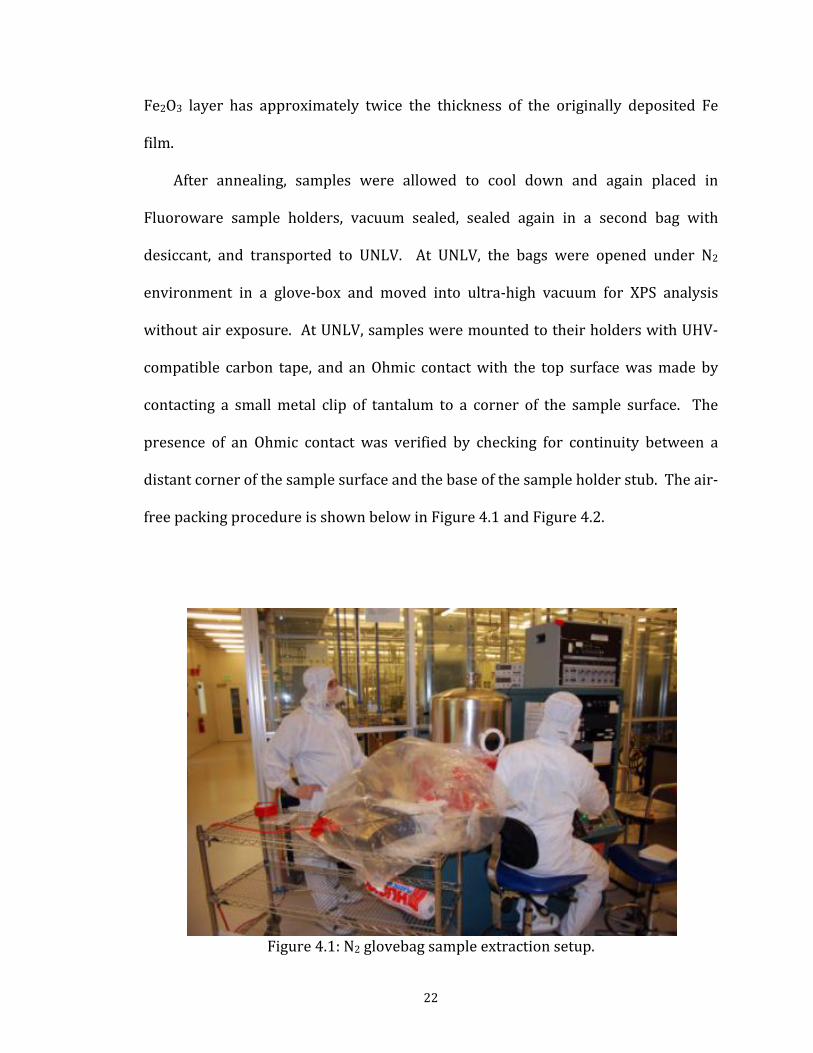
Fe2O3 layer has approximately twice the thickness of the originally deposited Fe film. nd again placed in second bag with e opened under N2 m for XPS analysis holders with UHV-rface was made by mple surface. The ntinuity between a older stub. The air- 4.2.
p.
After annealing, samples were allowed to cool down aFluoroware sample holders, vacuum sealed, sealed again in adesiccant, and transported to UNLV. At UNLV, the bags werenvironment in a glove-box and moved into ultra-high vacuuwithout air exposure. At UNLV, samples were mounted to theircompatible carbon tape, and an Ohmic contact with the top sucontacting a small metal clip of tantalum to a corner of the sapresence of an Ohmic contact was verified by checking for codistant corner of the sample surface and the base of the sample hfree packing procedure is shown below in Figure 4.1 and Figure
22 Figure 4.1: N2 glovebag sample extraction setu
up.
samples are being l presence of beam-st scans of the Fe 2p ess of 475 nm was tandard survey and p and O 1s peaks a total of ten scans. ussed in Chapter 5, these scans show no spectroscopic evidence of beam-induced damage.
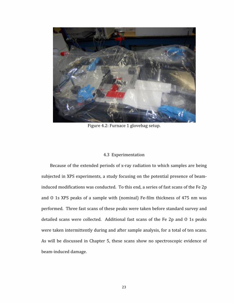
Figure 4.2: Furnace 1 glovebag set4.3 Experimentation Because of the extended periods of x-ray radiation to whichsubjected in XPS experiments, a study focusing on the potentiainduced modifications was conducted. To this end, a series of faand O 1s XPS peaks of a sample with (nominal) Fe-film thicknperformed. Three fast scans of these peaks were taken before sdetailed scans were collected. Additional fast scans of the Fe 2were taken intermittently during and after sample analysis, forAs will be disc
23

XPS survey scans were taken of all samples, followed by detailed scans of areas of interest. XPS scans from different samples were examined and compared against differences. The ied, and these data d used to develop nce. also examined. An f 50 nm of Ti on the x-ray source in the corded, followed by mple on the sample ’s Lindberg/Blue M in the VG SCIENTA el for the effect of with a PSIA XE-70 E anasinghe. Images l as annealed and g “mystery” sample
results of these experiments are presented and discussed in Chapter 5 of this thesis.
each other to identify common features, as well as meaningful chemical composition of elements in the samples was quantifwere then correlated to UCSB data on sample performance anmodels explaining sample composition and its effect on performaThe effect of the calcination step on the Ti/Pt interface wasunheated sandwich sample, consisting of 150 nm of Pt on top oquartz substrate, was examined with a monochromatized Al KαVG SCIENTA XPS system at UNLV. A baseline spectrum was reiterative measurements after discrete periods of heating the saholder stage. Another sample was annealed in air in UNLVfurnace at 700°C for four hours, and then also examined by XPSsystem. These spectra were then analyzed to develop a modcalcination on the Ti/Pt interface. The morphology of the sample surfaces was imaged in air non-contact Atomic Force Microscope (AFM) by Dr. Asanga Rwere taken of annealed and unannealed Fe-coated samples, as welunannealed Pt surfaces. Images of the anomalous, outperforminwere also collected and examined. The
24

CHAPTER 5 T ND DISCUSSION imental Quality Control Figure f a reference Pt spectrum.
200 100 0
RESUL S A5.1 Sample and Exper 5.1 shows a typical XPS survey scan o
1000 900 800 700 600 500 400 300
XPS
C 1s
.u.)
y (eV)
ference foil
Ar
Mg Kα
Inte
ns
Pt4f7/2
Pt 4f5/2
Pt 4d5/2Pt 4d3/2
Pt 4p3/2
Pt 4p1/2Pt 4s
ity (a Pt Re
Binding Energ l.
f the surface that is element-specific and highly instructive about the chemical environment. Line positions of reference metals can also be used to calibrate the XPS system, and by
Figure 5.1: XPS spectrum of a reference Pt foiThe shape and position of the peaks give a detailed view o
25

comparing the binding energy position Pt 4f7/2 peak of a sputtered Pt foil surface in Figure 5.1 against that of a reference Pt spectrum [25], we were able to verify the e to some materials rays on the sample re. Beam damage 1s and Fe 2p peaks, re to radiation.
6
energy axis alignment of our XPS system and all presented spectra.Because x-ray irradiation has been shown to be destructiv[26,27], it was first necessary to determine the impact of x-surface and, in particular, its electronic and chemical structustudies were conducted by recording baseline spectra of the O and then observing changes to the spectra after extended exposu
536 534 532 530 528 52
O 1s
nergy (eV)
Nor
mal
ize
Inte
nsity
(a.u
.)
Binding E
Scan 10Scan 9Scan 8Scan 7Scan 6Scan 5Scan 4Scan 3
XPSMg K
α
Figure 5.2: Series o -induced damage during a 4-hour radiation exposure.
Scan 2Scan 1
f O 1s XPS spectra to monitor possible beam
26

Figure 5.2 above shows the spectra for ten scans of the O 1s peak taken over four hours of exposure to Mg Kα radiation at 1253.6 eV. The spectra are offset in a ble deterioration in re 5.3 below) show
710
waterfall pattern for visual purposes only and show no appreciathe O 1s signal over this time period. The Fe 2p peaks (Figusimilar stability over the four hour exposure.
Scan 10Scan 9Scan 8Scan 7Scan 6Scan 5Scan 4Scan 3Scan 2
Inte
nsity
(a.u
.)
Fe 2p1/2 Fe 2p3/2
Scan 1
730 725 720 715
Binding Energy (eV)
XPS
Figure ctra to monitor possible beam-ure. 1s or Fe 2p peaks, the samples are proven to be durable enough for XPS experimentation and results can be presented as representative of the samples as provided.
Mg Kα
5.3: Series of Fe 2p1/2 and Fe 2p3/2 XPS speinduced damage during a 4-hour radiation exposWith no changes in shape or relative intensity in either the O
27

This experimental series also confirms that the sample grounding technique described in Chapter 4 sufficiently allows charge transfer across the Fe2O3 surface, f these spectra. d by the McFarland distinct batches, on igh performing PEC ed throughout this ecifically for UNLV’s sample numbers as
me e PFe thickness
(as deposited) Furnace name
with no peak shifting due to charge buildup being shown in either oThe α-Fe2O3 samples analyzed in this thesis were prepareuGro p at the University of California, Santa Barbara in three three separate occasions. The October 2008 batch produced hsamples that have not since been reproduced, and is referrdocument as the “Mystery Sample”. The first batch prepared spanalysis was prepared in December 2008, and is referred to bydescribed in Table 5.1 below.
Sample Na Dat rep ared“Mystery Sample” October 2008 10 nm Furnace 1Sample 1 Decembe Furnace 1r 2008 10 nmSample 2 December 2008 200 nm Furnace 1ple 3 mbe Furnace 1Sam Dece r 2008 400 nmSample 4 December 2008 800 nm Furnace 2 mbe Not CalcinedSample 5 Dece r 2008 0 nmSample 6 December 2008 10 nm Not Calcinedtro Furnace 20 nm Con l May 2009 0 nm10 nm Control May 2009 10 nm Furnace 2475 nm Con 475 nm Furnace 2trol May 2009Table 5.1: Table of sample descriptions
28 Initial evaluation of the December 2008 samples showed prominent C 1s peaks, suggesting surface contamination. Because of the surface-sensitive nature of XPS

analysis, the formation of an overlayer due to contamination, improper handling, or air exposure may greatly impact the results obtained from XPS spectra. The May trogen environment rocedure shown in
0
2009 samples were thus prepared as control samples under nias described in Chapter 4, and the results of the clean packing pFigure 5.4.
1000 800 600 400 200
10 nm Calcined(Furnace 1)
ember 2008
Inte
nsity
(a.u
.)
10 nm Calcined(Furnace 2)May 2009
Dec
Fe LVV
XPSMg K
αFe 2p1/2
Ti 2p1/2
Pt 4f5/2
C 1s
Fe 2p3/2 O 1sPt 4f7/2Pt 4p1/2
Pt 4d5/2
Binding Energy (eV)
Pt 4d3/2Pt 4p3/2
Ti 2p3/2
O KLL
C KVV
Fe LMM
le surface. d intensity at 200eV to discount differences in sample and x-ray source positions between measurements, and have been vertically offset to better show spectral details. The
Figure 5.4: Impact of clean packing procedure on sampThe two spectra in Fig. 5.4. were normalized to their backgroun
29
1shinsain
0 nm samp
caadh
dsh
hows signifn air (red sample. Thendicates decIt is impa
ple surface p
rbon-free; ir exposureuring the andling. The UCSeposited 50hows a mod
ficantly lessspectrum), ce cleaner sacreased Pt sportant to
prepared un
due to the e, we hypogrowth pro
SB Fe2O3 sa0 nm of Ti,del of the sa
Figu
s pronounceconfirming ample also signal attenunote that t
nder the ni
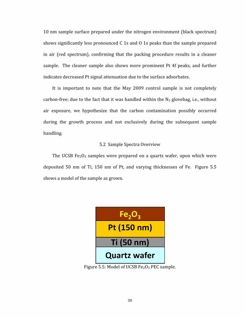
fact that it othesize thaocess and 5.2 Samamples wer, 150 nm oample as gro
ure 5.5: Mod30
ed C 1s and that the pashows moruation due tthe May 20
trogen envi
was handleat the carbnot exclusmple Spectrae prepared of Pt, and vown.
del of UCSB
O 1s peaksacking procre prominento the surfa009 control
ironment (b
ed within thbon contamively durina Overviewon a quartvarying thic
Fe2O3 PEC s
s than the scedure resunt Pt 4
black spectr
f peace adsorbat sample is he N2 glovebmination pong the subs
tz wafer, upcknesses of
sample.
ample prepults in a clerum)
aks, and furpared
tes. not compl
eaner r
bag, i.e., witossibly occu
ther etely
sequent sathout urred mple
pon which wf Fe. Figurewere e 5.5

Figure 5.6 shows an XPS spectrum of Sample 2, chosen as a representative Fe2O3 sample because its film thickness is the average of the thickest and thinnest nm) refers to the Fe erience of the UCSB tely twice as thick.
200 0
samples analyzed. Note that the film thickness given here (200 film thickness before calcination (i.e., as deposited). It is the expgroup that the resulting Fe2O3 film after calcination is approxima
Fe LVV
Inte
nsity
(a
Fe 2p1/2
Fe LMM
e 4 (200nm)e 2
1000 800 600 400
.u.)
SamplFurnac
Binding Energy (eV)
C KVV
O KLL
Fe 2p3/2
O 1s
Ti 2p
C 1s
Fe 3s
Fe 3p
XPSMg K
α
eaks dominate the spectrum, together with a substantial C 1s peak. The O 1s peak is pronounced and well defined, and peaks from several Fe orbitals are evident. The Ti peak, probably
Figure 5.6: UCSB Sample 4, representative Fe2O3 PEC sample. As would be expected for this sample, the Fe and O p
31

due to Ti originating from the substrate, indicates the presence of diffusion processes, as will be discussed in more detail in an upcoming section. The high is due to inelastic α-Fe2O3 sample (in s in the bulk of the A comparison of a igure 5.7 and Figure
200 0
background on the high binding energy side of the spectrumscattering of electrons stemming from deeper layers within theessence, each characteristic emission line associated with atomsample creates a step function towards higher binding energy).200 nm Fe sample with a 400 nm Fe sample is shown below in F5.8.
Sample 2 (200 nm)Furnace 1
Inte
nsity
(a.u
.)
1000 800 600 400
Binding Energy
3 (400 nm)Furnace 1Sample
XPSMg K
α
Fe 2p1/2
Fe 3sFe 3p
Fe 2p3/2
Ti 2p1/2
O 1s
C 1sTi 2p3/2
Fe LVV
Fe LMM
O KVV
C KVV
Figure 5.7: Comparison between Fe2O3 samples with 200 nm and 400 nm Fe film thickness before calcination. 32

The difference spectrum in Figure 5.8 was created by subtracting the spectrum of the thinner sample from that of the thicker sample, more clearly highlighting the o the background at ge. The difference of Sample 3 versus
00 0
differences between these samples. Due to the normalization t200 eV, the difference spectrum is close to zero in this ranspectrum also reveals the comparatively higher oxygen content Sample 2, and a slightly increased amount of Ti on the surface.
1000 800 600 400 2
XPSMg K
α
Δ In
tens
ity (a
.u.)
Ti 2p3/2
Binding Energy (eV)
O 1s
ample 3. The full series of the December 2008 survey spectra is plotted in Figure 5.9. Survey spectra present an overview of the entire energy range and are useful for quickly
Figure 5.8: Difference spectrum of Sample 2 versus S
33
estimating the composition of samples. The spectra shown have been normalized to the background at 274 eV, and offset vertically to facilitate comparison. Calcined spectra also reveal d titanium (for all epth of only a few of Pt and varying e technique clearly amples. Tellingly, samples. tion process, as will 10 nm nominal Fe h suggests that the -thick layer, but (at the Fe2O3 or in rface can also not be r (thicker) samples.
samples (1-4) are indicated by bold font. Beyond the expected iron, oxygen, and carbon, the surveythe presence of chromium (for Sample 2 and Sample 3) ancalcined samples). Although Mg Kα XPS has an information dnanometers, and Ti should be buried under a minimum of 150 nm thicknesses of Fe (or Fe2O3), the spectra of this surface-sensitivshow the presence of titanium on the surface of the calcined stitanium does not appear to be present on the surfaces of the non-calcined This indicates significant diffusion processes during the calcinabe described below. Note that the thinnest sample (sample 1,thickness) also exhibits peaks characteristic of platinum, whicformed Fe2O3 overlayer is not a completely homogeneous, 20-nmleast in some regions) allows XPS to detect Pt atoms either through regions between Fe2O3 islands. A diffusion of Pt atoms to the suruled out, but is less likely, since it is not seen for any of the othe
34

1000 800 600 400 200 0
Fe LMMIn
tens
ity (a
.u.)
Binding Energy (eV)
(0 nm)
Sample 1 (10 nm)
Sample 6 (10 nm)
Sample 2 (200 nm)
Sample 4 (200 nm)Sample 3 (400 nm)
Sample 5
C KVV O KLL Fe 2p O 1s
Ti 2pC 1s
Fe 3sFe 3p
Pt 4p1/2 Pt 4p3/2 Pt 4d3/2 Pt 4d5/2 Pt 4f
Cr 2p
XPSMg K
α
er 2008 (heated), additional les were performed
t 700°C for 4 hours After 4 hours, the furnace was automatically turned off with no controlled temperature ramp down.
Figure 5.9: Survey spectra of Decemb samples. Since Ti appears only in samples that have been calcined experiments inv perature on the sampand are describeestigating the effect of temd in Section 5.3. 5.3 Sample Preparation Findings
5.3.1 Effect of Calcination on Morphology October 2008 and December 2008 samples were annealed awith a 2°C ramp up in temperature to operating temperature.
35
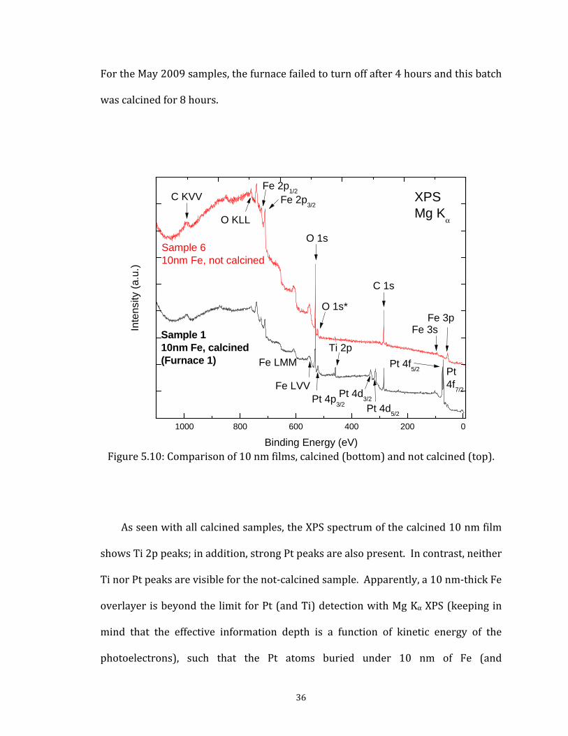
For the May 2009 samples, the furnace failed to turn off after 4 hours and this batch was calcined for 8 hours.
00 0
Sample 110nm Fe, calcined(Furnace 1)
Inte
nsity
(a.u
.)
XPSMg K
α
Sample 610nm Fe, not calcined
Pt 4p3/2
Fe LMM
Fe LVVPt 4d3/2
Pt 4d
Pt 4f5/2
C KVV
1000 800 600 400 2
Binding Energy (eV)
5/2
O KLL
Fe 2p1/2Fe 2p3/2
O 1s
C 1s
Ti 2p
Fe 3sFe 3p
O 1s*
Pt 4f7/2
not calcined (top). calcined 10 nm film In contrast, neither tly, a 10 nm-thick Fe Kα XPS (keeping in mind that the effective information depth is a function of kinetic energy of the photoelectrons), such that the Pt atoms buried under 10 nm of Fe (and
Figure 5.10: Comparison of 10 nm films, calcined (bottom) andAs seen with all calcined samples, the XPS spectrum of the shows Ti 2p peaks; in addition, strong Pt peaks are also present.Ti nor Pt peaks are visible for the not-calcined sample. Apparenoverlayer is beyond the limit for Pt (and Ti) detection with Mg
36

consequentially approximately 20 nm of Fe2O3) should not be visible. Spectra for both these samples were taken at the same incident angle to the x-ray source, so is not visible in the also be ruled out; occurring. e identical calcined ere taken of the two er completion of all morphology of the
Figure 5.11: (5 μm)2 AFM image of the 10 nm thick uncalcined Fe film.
angular effects can be ruled out. Furthermore, since the Pt layer uncalcined samples, porosity of the as-deposited film can however, a morphology change in the film due to heating may be To examine the morphological differences between otherwisand uncalcined films, Atomic Force Microscope (AFM) images wsamples. Samples were removed from vacuum for imaging aftXPS experiments. Figure 5.11 and Figure 5.12 show the surface10 nm uncalcined Sample 6.
37
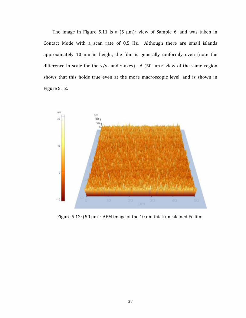
The image in Figure 5.11 is a (5 μm)2 view of Sample 6, and was taken in Contact Mode with a scan rate of 0.5 Hz. Although there are small islands ly even (note the of the same region l, and is shown in
.
approximately 10 nm in height, the film is generally uniformdifference in scale for the x/y- and z-axes). A (50 μm)2 view shows that this holds true even at the more macroscopic leveFigure 5.12.
Figure 5.12: (50 μm)2 AFM image of the 10 nm thick uncalcined Fe film
38

lcined Fe2O3 film. e surface of the film growth, with peaks in the uncalcined ith negative depths. g at the Fe2O3 layer island grows. This nm film, but does formation and its may be due to the outgrowth of either the Pt or Ti layers into and through the Fe2O3 layer.
Figure 5.13: (5 μm)2 AFM image of the 10 nm thick caAfter calcination at 700 °C for 4 hours, distinct changes to thare seen, as shown in Figure 5.13. shows increased island approximately 30 nm in height (i.e., about three times as high as case in Figure 5.11). The AFM image also shows more regions wThis may be due to several reasons – island formation is occurrinand there is a dewetting effect that reveals the substrate as thewould explain the Pt peaks in the XPS spectrum of the calcined 10 not account for the presence of Ti. Alternatively, this islandcorresponding holes
39

To better investigate these theories, it is necessary to better understand the Ti/Pt interface without the additional Fe/Fe2O3 variables. This was done by heating and by studying the
0 0
0 nm Fe (i.e., bare Pt film) samples to different temperatures surface composition in XPS survey scans. These spectra were also compared against a reference Pt foil, as shown in Figure 5.14.
1000 800 600 400 20
Sample 5(0 nm)Dec. 2008
0 nmM
Controlay 2009
Inte
nsity
(a.u
.)
Pt Reference Foil
Ar
C 1s
Mg Kα XPS
Pt4f7/2
Pt 4f5/2
Pt 4d5/2Pt 4d3/2
Pt 4p3/2
O 1s
Pt 4p1/2Pt 4s
O KLLC KVV
Binding Energy (eV) samples. or 3 hours to clean its surface before XPS examination. This results in a small Ar peak present in the reference spectrum that is not seen in the other two samples. The O 1s and C 1s
Figure 5.14: Comparison of reference Pt foil to Pt filmThe reference Pt foil was sputtered with Ar+ ions at 3 keV f
40

peaks seen in the grown samples are more prominent than in the sputter-cleaned reference foil, but similar to each other, regardless of the sample handling and is somewhat onditions. in air at 700°C in a in the VG SCIENTA her May 2009 0 nm ents for 30 minutes, Al Kα x-ray source.
extraction method. In fact, the O 1s signal of the 0 nm control sample larger, despite the fact that it was extracted under dry nitrogen cOne of the May 2009 0 nm control samples was heated Lindberg/Blue M furnace for 4 hours and examined by XPS system (to be discussed in conjunction with Figure 5.22). Anotcontrol sample was directly heated in vacuum in 100°C incremand immediately measured by XPS using the monochromatizedThe corresponding data is shown in Figure 5.15.
Inte
nsity
(a.u
.)
462 460 458 456 454 452
Binding Energy (eV)
30 min at 200° C
Baseline
30 min at 770° C (heating stage) 700° C (Pyrometer)
30 min at 700° C (heating stage)
30 min at 600° C (heating stage)
30 min at 500° C (heating stage)
at 400° C (heating stage)
30 min at 300° C (heating stage)
(heating stage)
XPSAl K
α
30 min
41
Ti 2p1/2
Ti 2p3/2
Figure 5.15: Emergence of Ti 2p peak in response to heating of a May 2009 0 nm control sample in UHV.

The sample temperatures given were measured by the thermocouple of the heating stage (indicated by “heating stage” in Figure 5.15). For the highest y with a pyrometer. rature versus the 0°C and 700°C the poor thermal ce. ating the sample to hermocouple scale), hermocouple scale. d 700°C on the t to understand the n additional sample le) for 4 hours and 0 °C (again on the n in Figure 5.16. is present already after 30 minutes of annealing, indicating that the process is relatively fast.
temperature, the sample temperature was also measured directlComparison of the displayed thermocouple-measured tempepyrometer-measured temperature showed readings of 77respectively. Since the samples are heated from below, conductivity of the quartz substrate may account for this differenAs is evident from Figure 5.15, Ti 2p peaks emerge after he700 °C on the pyrometer/sample surface scale (770°C on the twhile they are absent after annealing at 700 °C on the tApparently, Ti diffusion is initiated between 600°C anpyrometer/sample surface scale. In addition to the temperature dependence, it is importantime dependence of the observed Ti diffusion. To gain insight, awas heated at 705 °C (on the pyrometer/sample surface scacompared to a sample that was heated for 30 minutes at 70pyrometer/sample surface scale). The results are showApparently, a pronounced Ti signal
42

466 464 462 460 458 456 454 452 450
XPSAl K
α
Inte
nsity
(a.u
.)
Binding Energy (eV)
30 minute heating at 700°C
4 hour heating at 705°C
e emergence of a Ti inutes of heating at Figure 5.16: Ti 2p XPS spectra after heat treatment, showing thsignal from atoms diffusing to the Pt surface already during 30 m700 °C.
43

466 464 462 460 458 456 454 452 450
Inte
nsity
(a.u
.)
Ti 2p3/2
Ti 2p1/2
Annealed 4hrs at 700° C in air
Annealed 4hrs at 705° C in vacuum
Baseline sample
Ti 2p1/2
Ti 2p3/2
XPSAl K
α
Binding Energy (eV) annealing (bottom), re scale) , and after
rsus one heated in .17. Comparing the tra obtained after i peaks emerge as a shows the Ti 2p3/2 sample annealed in air has a Ti 2p3/2 peak position of 457.0 eV – indicative of a titanium oxide, most likely an intermediate form of TiO2.
Figure 5.17: Ti 2p spectra of a 0 nm Fe control sample before after annealing in UHV (center, 705 °C, pyrometer temperatuannealing in air (top, 700 °C). Finally, comparing a sample heated in air for 4 hours vevacuum for 4 hours completes the picture, as shown in Figure 5unannealed baseline sample (bottom), with the two specannealing in UHV (center) and air (top), it is evident that the Tresponse to the annealing step. The sample annealed in vacuumpeak at 453.6 eV (b.e.), indicating metallic titanium, whereas the
44

Scanning Electron Microscope (SEM) images were taken at UCSB to shed further light on the morphology of the PEC samples as a function of heating.
cross section). le after calcination. roughly doubled in shows an apparent me grain structure
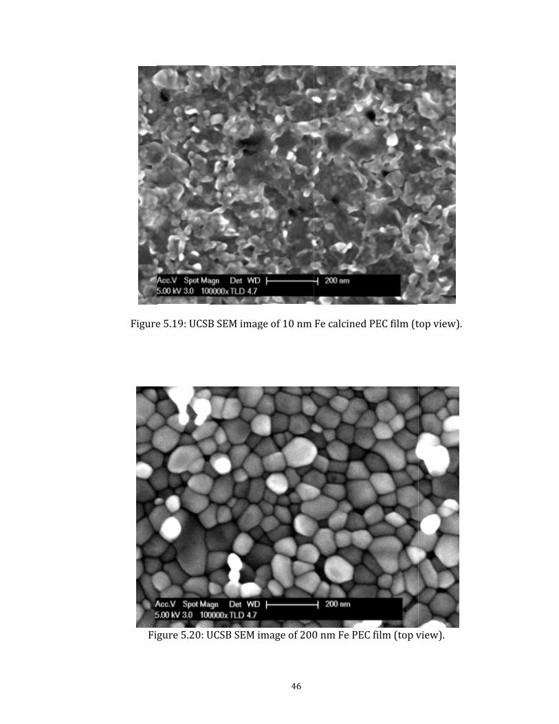
p-down view of the sample in Figure 5.19 shows a porous, small grained structure with some island formation (as seen in Figure 5.13), but accretion is not yet pronounced.
Figure 5.18: UCSB SEM image of the 10 nm Fe calcined PEC film (Figure 5.18 shows a cross sectional view of a 10 nm Fe sampConsistent with previous PEC Fe2O3 samples, the Fe layer hasthickness and, in this sample, is 23.9 nm thick. This thin sampledelamination between the Pt layer and the Fe2O3 layer, and soformation is evident within the Pt layer An SEM to
45
Figure
Fi
e 5.19: UCSB
gure 5.20: U
B SEM imag
UCSB SEM im46
ge of 10 nm
mage of 200
Fe calcined
0 nm Fe PEC
d PEC film (t
C film (top v
top view).
view).

pp5im
saoo
The surfarticles tharesent in it.21) showsmmediately
face of the 2
FiguThe inteample. Larn the surfabserved isla
an in the 1ts XPS spec that the iry at its interf
200 nm film
ure 5.21: UCerface betwge needle-liace of the 2ands reach u
0 nm film, ctrum. A crron oxide fiface to the P
m is more un
SB SEM imaween the Ti ike outcrop00 nm filmup to 80 nm
47
but, as shoross-sectionilm is porouPt layer.
niformly co
age of 200 nand Pt layppings with m, and AFM m in height.
own in Figunal SEM imus in its bu
overed by p
nm Fe PEC fers is less diameters analysis (F
ure 5.7, Ti mage of this ulk, and
ebble-like F
larg
film (cross sdistinct thaless than 20igure 5.22)
signals aresample (FiFe2O3
ge cavities e still igure exist
section). an in the 100 nm are vi shows tha
0 nm isible at the

nm Fe PEC film
i.e., Pt films without the 10 nm and 475 ted in Figure 5.23. is puzzling, for even PS (Figure 5.24). In age than the 10 nm alcined XPS spectra (Figure 5.25) shows significant changes occurring during this specific calcination.
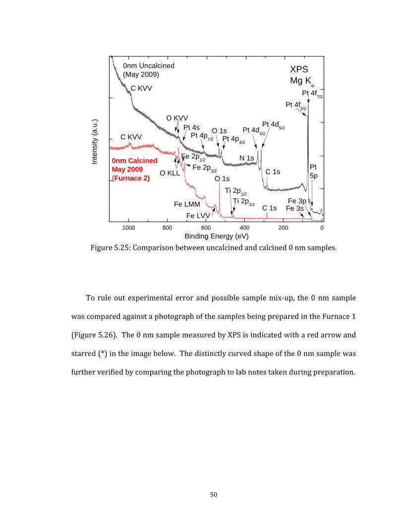
Figure 5.22: AFM image of 2005.3.2 Activity of Fe Due to Calcination During the May 2009 sample preparation, “0 nm” samples (Fe coverage) were calcined in Furnace 1 within the same tube asnm samples. The XPS spectrum for this 0 nm sample is presenThe complete lack of Pt peaks and presence Fe in the spectrum the thinnest calcined Fe films exhibit a noticeable Pt signal in Xfact, this nominally iron-free sample shows better Fe film coversample. A comparison between the uncalcined and c
48

1000 800 600 400 200 0
Fe 3p
nsity
(a.u
.)
SurveyXPSMg K
α
0 nm Fe, CalcinedMay 2009(Furnace 2)
O KLL
Fe 2p1/2Fe 2p3/2
O 1s
Ti 2p1/2
Ti 2p3/2C 1s
Inte
Binding Energy (eV)
Fe LMM
Fe LVV
Fe 3s
C KVV
O 2s
Fe 2s
alcined sample.
200 0
Figure 5.23: XPS spectrum of May 2009 0 nm c
1000 800 600 400
Inte
nsity
(a.u
.)
Binding Energy (eV)
0 nm Fe, CalcinedMay 2009(Furnace 2)
10 nm Fe, CalcinedMay 2009(Furnace 2)
C KVV
O KLL
Fe 2p1/2
Fe 2p3/2
XPSMg K
α
O 1s
Ti 2p1/2Ti 2p3/2
s
Fe 3sFe 3pFe LMM
Fe LVV
C 1
Pt 4f7/2Pt 4f5/2
Pt 4d5/2
Pt 4d3/2Pt 4p3/2
49 Figure 5.24: Comparison between 0 nm and 10 nm calcined samples.
1000 800 600 400 200 0
Inte
nsity
(a.u
.)
Binding Energy (eV)
Fe 3pFe 3s
O 1s
C 1s
0nm CalcinedMay 2009
ace 2)
XPSMg K
α
0nm Uncalcined(May 2009)
C KVV
O KVVPt 4s
Pt 4p1/2
O 1sPt 4p3/2
N 1s
Pt 4d3/2
Pt 4d5/2
C 1s
Pt 4f5/2
Pt 4f7/2
Pt5p(Furn
Fe LMMFe LVV
O KLL
C KVV
Fe 2p1/2
Fe 2p3/2
Ti 2p1/2
Ti 2p3/2
ed 0 nm samples. p, the 0 nm sample red in the Furnace 1 ith a red arrow and he 0 nm sample was further verified by comparing the photograph to lab notes taken during preparation.
Figure 5.25: Comparison between uncalcined and calcinTo rule out experimental error and possible sample mix-uwas compared against a photograph of the samples being prepa(Figure 5.26). The 0 nm sample measured by XPS is indicated wstarred (*) in the image below. The distinctly curved shape of t
50

Figure 5.26: Sample positions during calcination the 475 nm sample d from the 475 nm aining its complete way through which ples. ed at UCSB revealed SIMS analysis re seen in films of ever, the relative heating process. m the Pt layer, and ental techniques. ction limits on the order of parts per billion, it is a destructive technique that does not shed information about the surface of the sample, whereas XPS preserves the as-grown
The position of the 0 nm sample immediately adjacent to suggests that, during the calcination process may have desorbesamples and readsorbed (calcined) on the 0 nm sample, explcoverage with iron oxide. This finding may also suggest a pathother contaminants may have been introduced into the Fe2O3 sam5.3.3 Sample Contamination Secondary Ion Mass Spectrometry (SIMS) analysis performseveral contaminants in the calcined films. A December 2008 reported the presence of Cr and Al. These contaminants wewdifferent thicknesses, both before and after calcination – hoabundance of these contaminants appeared to be higher after theThe McFarland group suspected the contamination came froUNLV was asked to confirm their findings with our experimAlthough the SIMS technique is extremely sensitive with dete
51

state of the sample, but gives composition information with much lower sensitivity (approx. 0.1%). ents because of its f5/2 peaks at 71 and r, was in a binding r was the suspected ed Sample 5 was ak was found, and n in Fig. 5.29.
110
The primary Al 2p XPS peak was not useful in these experimposition at 74.4 eV, directly under the dominant Pt 4f7/2 and Pt 474 eV, respectively. The Al 2s peak at 118 eV (b.e.), howeveenergy region unobscured by other elements. Since the Pt layecause of contamination, this region of the platinum-surfacexamined, as shown in Figure 5.28. No indication of an Al peinspection of the other samples showed the same result, as show
130 125 120 115
Al 2s Region
.u.)
Binding Energy (eV)
Pt Reference Sample
0nm Sample (May 2009)
XPSMg K
α
Inte
nsity
(a
Sample 5 (December 2008)
52 Figure 5.27: XPS spectra of the Al 2s region of Pt samples.

130 128 126 124 122 120 118 116 114 112 110
XPSMg K
α
Sample 3 (400nm)
(a.u
.)
Sample 5 (0nm)
Sample 1 (10nm)
Sample 4 (200nm)
Sample 2 (200nm)
Sample 6 (10nm)Inte
nsity
Binding Energy (eV) ber 2008 samples. 5.9) confirmed the e Furnace 1. Detail spectral intensity in the presence of Cr
t for the presence of . During sustained and samples may be and adsorb unto other samples. This cycle of desorption, transport, and adsorption may not only affect samples of any particular batch – it can affect other samples prepared after
Figure 5.28: XPS spectra of the Al 2s region for DecemInitial survey spectra of the December 2008 samples (Figurepresence of chromium on Samples 2 and 3, both calcinated in thspectra of the Cr 2p region (Figure 5.30) indeed show enhancedthis region for samples 2 and 3, but do not unambiguously showin any other sample (within the noise level). The diffusion method described in Section 5.3.2 may accounCr in the Furnace 1 samples but not in the Furnace 2 samplesheating cycles, desorption of contaminants from walls contaminate and be transported through the furnace’s heating tu
53
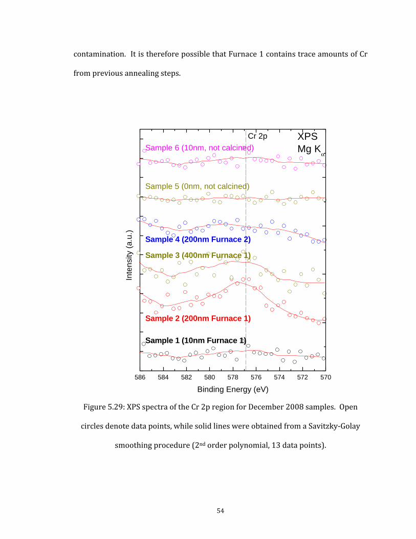
contamination. It is therefore possible that Furnace 1 contains trace amounts of Cr from previous annealing steps.
572 570
Sample 6 (10nm, not calcined
Sample 5 (0nm, not calcined)
Sample 4 (200nm Furnace 2)
Sample 3 (400nm Furnace 1)
Sample 2 (200nm Furnace 1)
Inte
nsity
(a.u
.)
)XPSMg K
α
Cr 2p
Sample 1 (10nm Furnace 1)
586 584 582 580 578 576 574
Binding Energy (eV) 08 samples. Open cir ined from a Savitzky-Golay smoothing procedure (2nd order polynomial, 13 data points).
Figure 5.29: XPS spectra of the Cr 2p region for December 20cles denote data points, while solid lines were obta
54

5.4 Furnace 1 and Furnace 2 Sample Differences With known performance differences between otherwise identical samples calcined in at the calcination process itself is ination. Figure 5.31 urs at 700°C in the
200 0
Furnace 1 and Furnace 2, it appears thintroducing differences into these samples in the form of contampresents the spectra for two 200 nm samples calcined for 4 horespective furnaces.
C KVV O KLL
Fe 2p1/2
Fe LMM
Fe 3sFe 3pIn
tens
ity (a
.u.)
Fe 2s
1000 800 600 400
Fe LVV
Binding Energy (eV)
Cr 2p
Fe 2p3/2
O 2sTi 2p1/2
O 1s
C 1s
Small Area ModeXPSMg K
α
Sample 4(200 nm,Furnace 2)
Sample 200 nm,
nace 1)
Ti 2p3/2
(2Fur
Figure 5.30: XPS spectra of Furnace 1 and Furnace 2 samples.
55

1000 800 600 400 200 0
C KVV
Fe LVV
Fe LMM
O KLL
C 1s
Fe 3p
Higher content in Furnace 2
Higher content in Furnace 1
Inte
nsity
(a.u
.)
O 1s
Ti 2p
Fe 2p1/2Fe 2p3/2
Binding Energy (eV)
Fe 3s
Cr 2p
Fe 2s
XPSMg K
α
Small Area Mode
u nace 2 samples. As with the other ut no Pt is visible. s not present in the y normalizing both subtracting the s added as a visual reference to the baseline. The Furnace 1 sample shows higher iron and oxygen content than the Furnace 2 sample. The Furnace 2 sample, however, has a higher
Figure 5.31: Difference spectrum of Furnace 1 and F rBoth samples show strong iron, oxygen, and carbon peaks.calcined samples, the Ti 2p peaks are present in these spectra, bThe Furnace 1 sample also shows a distinct Cr 2p peak that iFurnace 2 sample. The difference spectrum shown in Figure 5.32 was created bspectra to the low binding energy background at 200 eV, and Furnace 2 data from the Furnace 1 data. The dotted line wa
56

carbon content. As will be discussed in Section 5.6.4, this relative carbon content is an essential piece to understanding the performance difference puzzle. t in the Furnace 1 formance over the tates, its 3+ state is can result in p-type Furnace 2 samples. for the effect stery Sample” est because of their ce produced. With sults are to date still ples, a high quality for future analysis. and other UCSB 10 ystery Sample with ples. A difference racting the December 2008 spectrum from the Mystery sample spectrum, as shown in Figure 5.33.
The difference spectrum highlights the chromium presensample, which may partially contribute to the enhanced perFurnace 2 sample. Although Cr may exist in several oxidation smost stable, and therefore most likely in this sample – which doping of the Furnace 1 samples that is not occurring in the Further experimentation is necessary to definitively draw a conclusion of Cr on performance. 5.5 The “MyThe October 2008 Mystery Samples were of particular intersuperior performance compared to samples previously and sinno intentional change in the sample preparation process, the reirreproducible. Because of the limited quantities of these samsurvey scan of the sample was measured to preserve all featuresWith no immediately obvious differences between this sample nm hematite films, another spectrum was collected on the Mparameters exactly matching the 10 nm December 2008 samspectrum was then produced by subt
57

1000 800 600 400 200 0
"Mystery Sample"10nm Fe10/09/2008(Furnace 1)
Inte
nsity
(a.u
.)
Binding Energy (eV)
O 1s
XPSMg K
α
High Resolution Survey
Pt 4f5/2
C 1s
Pt 4f7/2Pt 4d5/2
Pt 4d3/2
Pt 4p3/2
O KLL
C KVV Ti 2p3/2
Ti 2p1/2
Fe LVVFe LMM
Fe 2p3/2
Fe 2p1/2
N KVV
Fe 3p
N 1s
Si 2sSi 2p3/2
Fe 3s
Ti 3p
O 2s
“Mystery Sample”.
200 0
Figure 5.32: High resolution survey spectrum of 10 nm
1000 800 600 400
XPSMg K
α
Inte
nsity
(a.u
.)
Binding Energy (eV)
Higher content in Mystery Sample
Higher content in Sample 1 (Dec. '08)
TiO2 shoulder
C 1s
O KLL
O 1s
Fe 2p1/2
Fe 2p3/2
Fe LVV
Fe LMM Ti 2p
Fe 3p
Pt 4fC KVV
58
Figure 5.33: Difference spectrum of Mystery Sample and Dec. ’08 10 nm Sample.

The close fit of the background to the baseline in the low binding energy region shows a good normalization fit of the two spectra. The Mystery Sample surface s well as stronger O d shoulder at 532.3 2.6 eV. The Mystery ut, as will be shown Sample due to the f these findings will ssion
g our XPS data, the its photoionization Scofield [28] were to C 1s. Note that nificant number of es by a factor of 2. mission function of n free path of the ation for the exact e analysis across the samples, i.e., the investigation of relative changes, is more precise.
contains significantly less carbon than the December sample, aand Fe signals. The O 1s peak for Sample 1 shows a pronounceeV, and this feature can be seen in the difference spectrum at 53Sample also shows more Pt than the December 10 nm sample, bin Table 5.3, the relative amount of Pt is higher in the Mysterysignificantly reduced carbon concentration. The significance obe further discussed in the subsequent “Discussion” section. .6 Discu55.6.1 Quantification of Composition To quantify the elemental composition of the samples usinarea under the dominant peak of each element was divided bycross-section at 1254 eV. For this purposes, cross-sections fromused, as listed in Table 5.2. Cross-sections shown are relativethese are calculated atomic cross sections, relying on a sigsimplifications, and thus can easily deviate from the correct valuThe here-computed compositions do not factor in the transthe analyzer or the energy-dependence of the inelastic meaelectrons. Thus, the calculations are only a rough approximcomposition of each sample, while a comparativ
59

Orbital: Fe 2p3/2 O 1s C 1s Pt 4f7/2 Pt 4f5/2 Ti 2p3/2Scofield Cross Section 10.54 2.85 1.00 8.89 6.97 5.22Table 5.2: Scofield ionization cross sections of selected elements [28] peaks, the combined area ummed. Table 5.3 XPS. Because of its 1.00) and the low low 0.1 % and thus
F P
Because of the overlap in the Pt 4f7/2 and Pt 4f5/2 under their peaks was used, and their cross-sections were sbelow shows the relative content of the main elements seen inhigh cross-section of 7.60 (relative to the cross section of C ofintensity of its 2p3/2 peak, the Cr concentration (if present) is benot listed in Table 5.3. Sample e O C t TiSample 1 (10 nm, Fur )nace 1 3.9% 32.4% 45.8% 7.7% 10.1%Sample 2 (200 nm Fu 1 . 44.5% % 0.0% 1.1%rnace ) 28 8% 25.6Sample 3 (400 nm Fu 1rnace ) 17.5% 67.0% 7.3% 0.0% 8.2%u 2 .7 62.0% 0.0% 5.6%Sample 4 (200 nm F rnace ) 7 % 24.7%10 nm Control 4.7% 79.8% 12.2% 2.1% 1.2%0.0% 12.70%475 nm Control 22.7% 14.2% 50.4%10 nm Mystery Sample 9.1% 62.4% 1.8% 14.0% 12.7%Table 5.3: Relative Surface Composition of Samp
60
les This composition analysis was correlated with IPCE performance data provided by UCSB. In general, a high IPCE is obtained from thin (10 and 20 nm) samples

annealed at 500°C, while intermediate thicknesses (100 nm) show much lower performance. At higher thickness (500 nm, not shown), IPCE increases again. If sses disappears. reasonably assume Ti – at least not in do. From the data fact suggests that ore, Sample 1 and the surface (the 10 mples, likely due to m Control sample). “stabilizing” effect ip rformance behavior lied bias, the 10 nm le the thick 400 nm r, a significant IPCE le IPCE response in e, it appears that the ponse and more of a catalytic response, possibly due to the Pt or Ti on the sample surface. This is not to say that a photocatalytic process is completely absent, for studies have shown that
annealed at 700°C, the performance dip for intermediate thickneBased on the Ti segregation series (Figs. 5.15-17), we can that the surfaces of films calcined at 500°C do not contain quantities detectable by XPS. In contrast, films calcined at 700 °Cin Table 5.3, the low Fe content of the thin 700 °C samples in these films might be better described as (Fe,Ti)Ox+Pt. Furthermthe Mystery Sample both show a higher content of Pt than Fe onnm Control sample shows a higher Fe:Pt ratio than the other sadeposition of additional Fe during calcination, as seen in the 0 nWe thus speculate that the titanium on the sample surfaces has a on IPCE performance, especially in the intermediate thickness regime, where the din performance is much less pronounced. The high Pt and Ti content might also help to explain the peseen in the IPCE experiments at UCSB. For example, with no appSample 1 and the Mystery Sample show no photoresponse, whiSample 3 does. With an applied bias voltage of 0.4V, howeveresponse is obtained from the 10 nm Mystery Sample. With littan unbiased system, but a dramatic increase with applied voltagperformance of the 10 nm Fe films is less of a photocatalytic res
61

Pt-TiO2 catalysts are not only photosensitive, but symbiotically overcome many of problems inherent in PEC oxides [29,30]. The bandgap of the Pt-doped Ti is smaller rt, and the presence ing recombination
shows the O 1s peaks of the various calcined samples. Note that the the other samples,
and absorbs more efficiently than that of its undoped counterpaof Pt in the sample increases the charge-separation time – hinder[29,30]. 5.6.2 Oxide Formation Figure 5.34spectral quality for Samples 2, 3, and 4 is lower than that forsince the spectra had to be taken from the survey scans.
62

O 1s SeriesXPSMg K
le 4 (200nm Furnace 2)
10nm Mystery Sample
10nm Control
Nor
mal
ized
Inte
nsity
α
475nm Control
Sample 3 (400nm Furnace 1)
Sample 2 (200nm Furnace 1)
Samp
Sample 1 (10nm Furnace 1)530.2 eV
536 534 532 530 528
Binding Energy (eV) lcined samples. t for all samples, the ng energy at about nced in the 10 nm ly large Ti/Fe ratio. nt with literature describing such a shoulder at 532.1 eV in TiO2 films [31]. These findings thus also
Figure 5.34: XPS spectra of the O 1s region for a variety of caApart from the main oxide line at 530.2 eV, which is presen10 nm samples also show a distinct shoulder at higher bindi532.2 eV. This second oxide component is particularly pronouFurnace 1 sample, which, according to Table 5.3, has a particularFurthermore, the binding energy of 532.3 eV is in close agreeme
63

spectroscopically suggest the presence of TiO2 on the surface of the 10 nm samples, most clearly for the 10 nm Furnace 1 sample. n of increasing film rmance. As Figure radually with film f the hematite films hologies with lower dérale de Lausanne nses for different eir low-surface-area py images may also ilms. Several oxide ting, with one study ne minute at 700°C isker growth occurs s may help facilitate aining the detection p has proposed that may positively impact hematite’s performance as a photoanode [35]. Doping by Ti works by
5.6.3 Film Thickness & Morphology Apart from the variations of surface composition as a functiothickness, the morphology of the films also impact their perfo5.19 and Figure 5.20 showed, accretion of Fe2O3 occurs gthickness. The pebble-like structure increases the surface area oand increases the photoelectric performance compared to morpsurface areas. The Grätzel Group at the Ecole Polytechnique Féhave published findings that show different photorespomorphologies, with high-surface-area samples outperforming thcounterparts [32]. For this reason, the needle-like growth seen in the microscobe responsible for improving the performance of the thicker fstudies have reported the growth of “whiskers” after metal heashowing this phenomenon appearing with Fe2O3 after only o[33]. Voss, Butler and Mitchell have also suggested that this whas hollow tubes described as “tunnels” [34]. These internal voidTi diffusion through the sample from the inside of the film – explof Ti by XPS even on the thickest Fe2O3 films. The Grätzel groudoping the whiskers themselves (described as nanostructures)
64

producing Fe2+ cations in the Fe2O3 lattice – creating donor sites that n-dopes the hematite material [36], and this very effect is likely taking place in the thick films. ickness and carbon h May 2009 control this rule, however.
efinitively state that eriments performed ed on the surface, or and gentle ight be suitable to is, it is sufficient to t the hematite film n the sample, an Carp, Huisman, tivity due to surface ticularly identifying attenuation due to m seen are fewer than the total number of photons directed to the surface – negatively impacting IPCE performance.
Table 5.3 also shows an inverse relationship between film thcontent for samples prepared in the December 2008 batch. Botsamples and the October 2008 Mystery sample do not followThe significance of this will be discussed in the next subsection. 5.6.4 Carbon The surface sensitivity of the XPS technique allows us to dcarbon is on the surface of the observed samples; however, expto date do not allow us to determine if this carbon is only localizincorporated into the sample itself. Future angle resolved experiments surface cleaning via sample warming or mild ion sputtering mbetter answer this question, but for the purposes of this thesdemonstrate that the mere presence of C appears to impacperformance. Having determined the positive effect of TiO2 doping ounderstanding of the interaction of C and TiO2 is now necessary.and Reller have described the deactivation of TiO2’s photosensicontamination by materials with higher adsorption ability – parorganics as a well-known culprit [37]. Furthermore, photoniccarbon eans that the photons by the photoreactive species
65

The relatively lower carbon content of the thicker samples may explain the improvement in IPCE performance as film thicknesses increase. The source of this C ly since the Mystery ent. ay 2009, 475 nm ttention to limiting higher carbon levels m sample prepared er relative carbon expected). A closer ng. eam evaporation of e desired evaporant ced into the e-beam e 5.35).
contamination, however, still remains to be discussed, especialSample is characterized by an extremely low carbon surface contParticularly puzzling is the high carbon content of the Mh p a mcontrol sample. T is sam le was prep red with eticulous aatmospheric exposure and possible contamination – yet shows than samples prepared without this care. Furthermore, the 10 non the same day and under the same conditions, shows a lowcontent than the 10 nm sample prepared in December 2008 (aslook at the sample preparation process may rationalize this findiAs discussed in Chapter 4, films are prepared by electron-bthe metals unto the substrate, forming thin layers. Pellets of th(metal) are placed into a graphite crucible, which is in turn plaevaporator (Figur
66

raphite crucible.
ystem. White arrows m that show damage and exposure of the crucible material (carbon).
Figure 5.35: Fe granules in new g
Figure 5.36: Fe-filled graphite crucible after use in the e-beam spoint at regions in the crucible wall and botto
67

The electron beam is rastered across the granules to prevent uneven heating and “spitting” due to hot spots; however, care has to be taken to avoid contacting the n crucible after use. re damaged by the in this image was fically for any of the lustrative only. The pletely through the his type of damage. oncentration of the rn-through of the crucible. Crucible arbon into the films lains why samples bon content. (Even lly different carbon
ing films produced hindering Fe2O3 e film thicknesses, these samples out-performed their non-Mystery counterparts, and even after one year of storage in air, the 10 nm Mystery sample had lower carbon content than any
side walls of the crucible. Figure 5.36 shows an Fe-filled carboWhite arrows point to spots of the carbon crucible that weelectron beam. It is important to note that the crucible shownused to prepare an earlier batch of Fe2O3 samples, but not specisamples discussed in this thesis. For this reason, the image is ilarrow to the lower left shows where the beam has sliced comcrucible, while the arrow to the right shows the beginning of tThe center arrow shows the formation of a hole due to the celectron beam within the center of the crucible. A complete buelectron beam will result in cutting through the bottom of thedamage due to either cracking or burn-through will introduce cin an uncontrolled and undesired manner. The variability of this metal evaporation process expprepared in different batches may have such widely varying carthe control samples prepared on the same day have drasticacontent because they were prepared in two separate batches.) Finally, the extremely low carbon content in the best performat UCSB strongly support the theory of carbon photoelectrochemical water splitting performance. Across th
68

of the samples measured shortly after synthesis. As originally suspected, the key to high-performing iron oxide PEC films may indeed lie in contamination – just not in the manner initially suspected.
69
CHAPTER 6 ND FUTURE WORK mary This thesis erization of α-Fe2O3 thin films for b p at the University depositing 50 nm iron upon a quartz r 4 hours at 700°C. by UCSB identified um. UNLV’s X-ray nce of Cr in some of by XPS. UNLV was UCSB showed the s a function of film ms, to well-formed owed the growth of Air Atomic Force ce of islands on the
Before performing extensive XPS experiments at UNLV, the samples were tested to determine their durability under ionizing x-ray radiation. Beam damage tests
SUMMARY A6.1 Sum descr charactibed the photoelectrochemical applications, grown y the McFarland Grouof California, Santa Barbara. Samples were grown by sequentiallyof titanium, 150 nm of platinum and varying thicknesses of substrate. These films were then annealed (calcined) under air fodSecondary Ion Mass Spectroscopy (SIMS) analysis conducteseveral contaminants, including lithium, chromium, and aluminPhotoelectron Spectroscopy (XPS) was able to confirm the presethe samples, and rule out aluminum at the levels detectable unable to confirm or rule out lithium in the sample. Scanning Electron Microscopy (SEM) images taken by formation of pebble-like hematite particles that appear to grow athickness, ranging from indistinct features in the 10 nm filpebbles by 200 nm films. Cross-sectional SEM images also shneedle-like whiskers growing from the sample’s surface. Microscopy (AFM) imaging at UNLV also showed the emergensurface of the films.
70

were performed and confirmed the durability of the sample under extended irradiation. ples that had been s performed, and inum cover layer at a Pt-covered Ti film Ti diffusion through presence of TiO2 at d by measuring the IPCE data taken at s inversely impacts lowering the IPCE tion in the samples ition process, thus ry” performance of
exclusively on the ronic structure of standing, modeling and predicting their behavior. The Heske Group at UNLV has previously produced an all-experimental picture of the electronic properties at a WO3 thin film surface –
XPS analysis also showed titanium on the surface of samiment acalcined. A temperature-dependent heating exper wshowed that titanium emerges through the 150 nm-thick platabout 700°C. Further experimentation showed that annealing in air produced titanium oxide at the surface – showing that the the samples is a temperature-related phenomenon, and that thethe surface can aid in PEC activity. The relative composition of each PEC sample was quantifiearea under dominant XPS peaks. Comparison of these data withUCSB showed that the relative carbon surface content of sampletheir photocatalytic response, with higher carbon levels performance. This thesis proposes that the carbon contaminastems from the graphite crucibles used during the film depossuggesting an explana origin of superior “mystetion for the bon levels at thsamples with unusually low car e surface. 6.2 Future Work The characterization work covered in this thesis focusedphysical properties of the α-Fe2O3 films, but the electphotoelectrochemical materials is equally important to under
71

disproving several basic assumptions about the material in the process. Such a picture of Fe2O3 would be valuable in determining its true viability as a PEC amples possible, for d impact their band ed by introducing a his sample can then e2O3 (using a very UHV system). This yer and minimize Ti
d within the UHV transferred to the purity. Ultraviolet can experimentally hotoemission (IPES) entally determining e surface. tu analysis of Fe2O3; ntly has capabilities ng soft x-ray photon-in-photon-out spectroscopy– a crucial first step towards this. Such an experiment will provide insights into the chemistry of the material during
material. Experiments of this nature require the least-contaminated seven trace amounts of contamination can dope the samples anstructures. Such a prototypical α-Fe2O3 sample can be preparhigh purity iron foil into our ultra-high vacuum (UHV) system. Tbe annealed at high temperature under high purity O2 to form Frecently completed oxygen annealing chamber connected to theapproach would circumvent the need for the titanium binding lacontamination due to diffusion through the system. The crystal structure of the iron oxide surface can be evaluatesystem by Low Energy Electron Diffraction (LEED), and thenAnalysis Chamber for XPS analysis to confirm the sample Photoelectron Spectroscopy (UPS) within this same chamber determine the valence band edge of the sample, while Inverse Pican determine the conduction band edge – thus, in total exper mthe Fe2O3 band gap, band edge positions, and work function at thMore long-term planned experimentation involves the in-siunder PEC-like conditions in electrolyte. The Heske group curreat Beamline 8.0 at the Berkeley Lab’s Advanced Light Source to analyze liquids usi
72

the photoelectrochemical process, in particular in view of photochemical degradation.
73

74
BIBLIOGRAPHY [1] Gueymard, C.A.; The sun’s total and spectral irradiance for solar energy applications and solar ra s. Solar Energy 2004, 76, 423–453.
e Earth System efs/ed-stickler/ed-autics and Space m.pveducation.org/ Education Network, Atmosphere, "U.S. ric Administration, States Air Force,
renewable energy ncy. 7/17/2007. d 11/15/2009). vanced Technologies l (accessed October iles.honda.com/fcx--environment/coal-/2009). World Coal of Water at a system simulation
[12] Turner, J.; Deutsch, T.; Leisch, J.; Wang, H.; Photoelectrochemical Systems for H2 Production. DOE Hydrogen Program FY 2005 Progress Report.
diation model9[2] Stickler, G.; Kyle, L.; Solar Radiation and thhttp://edmall.gsfc.nasa.gov/inv 9Project.Site/Pages/science-britm ssed October 2, 2009). National Aer nirradiance.h l (acce oAdministration (NASA). [3] International standard ISO 9845-1, 1992. http://pvcdroAPPEND/Am1_5.htm (accessed October 2, 2009). Photovoltaic ASTM G-173-03. e t[4] United States Committee on Ext nsion o the StandardStandard Atmosphere, 1976", National Oceanic and AtmospheNational Aeronautics and Space Administration, United Washington D.C., 1976. [5] Barbir, F.; PEM electrolysis for production of hydrogen from sources. Solar Energy 2005, 78, 661–669. [6] World Energy Council. Fuel Cell efficies/377.asp. (accessehttp://www.worldenergy.org/focus/fuel_cell[7] U.S. Department of Energy, U.S. Environmental Agency. Ad
& Energy Efficiency. http://www.fueleconomy.gov/feg/atv.shtm7, 2009). H Cl[8] onda FCX arity – Fuel Cell Comparison. http://automobclarity/fuel-cell-comparison.aspx (accessed 11/16/2009). S o .o tt e 1 1[9] IGCC, upercritical. http://www.worldc al rg/coal- heuse-the-environmen /improving-effici ncies/ (accessed 1/ 6Institute. [10] Fujishima, A.; Honda, K.; Electrochemical PhotolysisSemiconductor Electrode. Nature 1972, 238, 37-38. [11] Ulleberg, Ø.; Modeling of advanced alkaline electrolyzers: aapproach. Int. J. Hydrogen Energy 2003, 28, 21-33.

[13] Bak, T.; Nowotny, J.; Rekas, M., Sorrell, C.C.; Photo-electrochemical hydrogen generation from water using solar energy. Materials-related aspects. Int. J. Hydrogen Energy 2002, 27, 991-1022. .; Environmental yst? A Comparative 1-169. rner, J.; Theory of [Online] 2008 r.pdf (accessed
nt Thin Film Fe2O3 structure-Directing in metal oxides: A , 144305. nn. Physik 1887, 31, rostatisch geladene
, M.P.; Practical S iley & Sons Ltd., nth Edition, Oxford , Hydrogen. Solar r Science+Business
aterials, (2009), ards_review.html. ecoupled XY and Z
tes Artifacts from Cross-Talk in Images, 2007, http://www.nanotech-now.com/news.cgi?story_id=22812 (accessed November 13, 2009).
[14] Kormann, C.; Bahnemann, D.W.; Hoffmann, M.RPhotochemistry: Is Iron Oxide (Hematite) an Active Photocatal3 J. oc to ., AStudy: α-Fe2O , ZnO, TiO2. Phot hem. Pho biol 1989, 4, 16[15] Huda, M.; Walsh, A.; Wei, S-H.; Yan, Y.; Al-Jassim, M.; Tuo .eOxides for Photoelectrochemical Hydrogen Producti nhttp://www.hydrogen.energy.gov/pdfs/review08/pdp_34_turnMay 2, 2009). [16] Cesar, I.; Kay, A.; Martinez, Jos A.; Grätzel, M.; TranslucePhotoanodes for Efficient Water Splitting by Sunlight: NanoEffect of Si-Doping. J. Am. Chem. Soc. 2006, 128, 14. [17] Iordanova, N.; Dupuis, M.; Rosso, K.M.; Charge transporttheoretical study of hematite α-Fe2O3. J. of Chem. Phys. 2005, 122[18] Hertz, H.; Über sehr schnelle elektrische Schwingungen, A421. [19] Hallwachs, W.; Über den Einfluβ des Lichtes auf elekt1888, 33, 301. Körper, Ann. Physik
urface Analysis W[20] Briggs, D.; Seah , John Chicheser, England (1990). [21] Atkins, P.; de Paula, J.; Atkins’ Physical Chemistry, SeveUniversity Press, Oxford, England (2002). [22] Grimes, C.A.; Varghese, O.K.; anjan, S.; Lig t, R h WaterGeneration of Hydrogen by Water Photoelectrolysis. SpringeMedia, LLC., New York City, NY USA (2007). [23] Measurements of PEC hydrogen production mhttp://www2.eere.energy.gov/hydrogenandfuelcells/pec_stand(accessed November 13, 2009). U.S. Department of Energy. [24] Park Systems. Park Systems New XE-70 AFM/SPM with DScanners Elimina
75

[25] Moulder, J. F.; Stickle, W. F.; Sobol, P. E.; Bomben, K. D.; Handbook of X Ray Photoelectron Spectroscopy: A Reference Book of Standard Spectra for Identification and Interpretation of XPS Data; Physical Electronics, 1995. mic Press, Orlando,
ronic surface level production. J. Phys.
s-sections at 1254 7. ciency using Pt-TiO2 en, D.; Park, J-N.; hotoelectrochemical rova, V.; Spassov, L.; . of Phys.: Conference
Thin Film ht: Nanostructure-583. emperature. J. Phys.
te Blades during the 929-935. Photooxidation by 15714-15721. ontaining Titanium. [37] Carp, O.; Huisman, C.L.; Reller, A.; Photoinduced reactivity of titanium dioxide. Prog. Solid State Chem. 2004, 32, 33-177.
[26] Park, R. L.; Lagally, M. G.; Solid State Physics: surfaces. AcadeFL USA (1985). lum, M.; Bär, M; [27] Weinhardt, L.; B and Heske, C.; Electpositions of WO thin films for photoelectrochemical hydrogen3Chem. C, 2008, 112, 3078-3082. [28] Scofield, J.H.; Hartree-Slater Subshell Photoionization Cros3and 1487 eV. J. Electron. Spectrosc. Relat. Phenom. 1976, 8, 129-1f[29] Li, F.B.; Li, X.Z.; The Enhancement of photodegradation ef icatalyst. Chemosphere 2002, 48, 1103-1111. [30] Hu, Y-S.; Kleiman-Shwarsctein, A.; Forman, A.J.; HazMcFarland, E.W. Pt-Doped α-Fe2O3 Thin Films Active for PWater Splitting. Chem. Mater. 2008, 20, 3803-3805. [31] Stefanov, P.; Shipochka, M.; Stefchev, P.; Raicheva, Z.; LasaXPS characterization of TiO2 layers deposited on quartz plates. JSeries 100 2008, 012039. [32] Cesar, I.; Kay, A.; Gonzalez Martinez, J.; Grätzel, M.; Translucent Sunlig582-4Fe2O3 Photoanodes for Efficient Water Splitting by Directing Effect of Si-Doping. J. Am. Chem. Soc. 2006, 128, 4[33] Takagi, R.; Growth of Oxide Whiskers on Metals at High TSoc. Jpn. 1957, 12 (11), 1212-1218. [34] Voss, D.A.; Butler, E.P.; Mitchell, T.E.; The Growth of HematiHigh Temperature Oxidation of Iron. Metall. Trans. A 1982, 13A, [35] Kay, A.; Cesar, I.; Grätzel, M.; New Benchmark for WaterNanostructured α-Fe2O3 Films. J. Am. Chem. Soc. 2006, 128 (49),[36] Morin, F. J.; Electrical Properties of αFe2O3 and αFe2O3 CPhys. Rev. 1951, 83 (5), 1005-1011.
76

77
VITA Graduate College U sity of Nevada, Las Vegas . George
Degrees: Bachelor of sGraduate & Professional Student Association (GPSA)
ttee Graduate Council overnor’s Cup aduate Council ur Society ip (UNLV) larship (UNLV)
ronic structure of lum, K. George
niver Kyle E. N Arts, C hemist y, 2008as Vegas r:
University of Nevada, LrdV
Special Honors and AwaVice President – UNLChair, UNLV GPSA Grants Committee m Committee -hoc Commimittee Chair, UNLV GPSA Research ForuChair, UNLV GPSA Government Relations Adoc ComChair, UNLV GPSA Budget Crisis Ad-hChemistry Representative – UNLV Colate Commenclege of Sciencesement Speaker ernor’s Cup 2008 UNLV Undergradu2008 UNLV Distinguished Graduate 2nd Place – Tri-State 2008 Reynolds Gov1 Place – Nevada State 2008 Reynoldst ds GergrohChair – UNLV College of Sciences UnMember – Golden Key International HonRecipient – Carter G. Woodson ScholarsRecipient – Renee & Martin Paluga Scho Publications:
“Impact of air-exposure on the chemical and electZnO:Zn3N2 thin films”, M. Bär, K.-S. Ahn, Y. Yan, L. Weinhardt, O. Fuchs, M. B , S. Heske, Pookpanratana, W. Yang, J.D. Denlinger, M. Al-Jassim, and C. Appl. Phys. Lett. 94, 012110 (2009). (3 pages)
Thesis Title: Characterization of Fe2O3 Thin Films for Photoelectrochemical at. Committee Member, Dong-Chan Lee, Ph.D. Graduate Faculty Representative, James Selser, Ph.D.
Hydrogen Production Thesis Examination Committee: Chairperson, Clemens Heske, Dr. rer. nCommittee Member, David Hatchett, Ph.D.