characterization of integrated nano materials - nist. a. martinez et al., jap, 104, 073708...
TRANSCRIPT
1
2007
© CEA 2009. All rights reserved Any reproduction in whole or in part on any medium or use of the information contained herein
is prohibited without the prior written consent of CEA
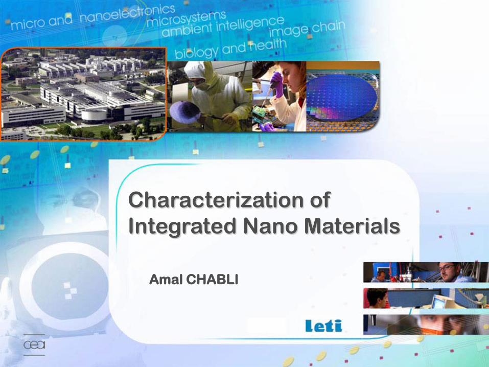
Characterization of Integrated Nano Materials A. Chabli
Characterization of Integrated Nano Materials
Amal CHABLI

2
2007
© CEA 2009. All rights reserved Any reproduction in whole or in part on any medium or use of the information contained herein
is prohibited without the prior written consent of CEA
Characterization of Integrated Nano Materials A. Chabli
300mm facility 200mm MEMS facility Nanocharacterization
From Europe - France
http://www.minatec.com
Micro and nano technologies
3
2007
© CEA 2009. All rights reserved Any reproduction in whole or in part on any medium or use of the information contained herein
is prohibited without the prior written consent of CEA
Characterization of Integrated Nano Materials A. Chabli
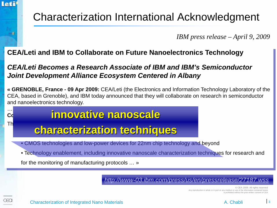
Characterization International Acknowledgment
http://www-03.ibm.com/press/us/en/pressrelease/27187.wss
CEA/Leti and IBM to Collaborate on Future Nanoelectronics Technology
CEA/Leti Becomes a Research Associate of IBM and IBM’s Semiconductor Joint Development Alliance Ecosystem Centered in Albany
« GRENOBLE, France - 09 Apr 2009: CEA/Leti (the Electronics and Information Technology Laboratory of the CEA, based in Grenoble), and IBM today announced that they will collaborate on research in semiconductor and nanoelectronics technology.…Complementary expertise This collaboration will focus on three key areas:
• Advanced lithography for fast prototyping and 22nm chip technology
• CMOS technologies and low-power devices for 22nm chip technology and beyond
• Technology enablement, including innovative nanoscale characterization techniques for research and
for the monitoring of manufacturing protocols … »
IBM press release – April 9, 2009
innovative nanoscalecharacterization techniques
4
2007
© CEA 2009. All rights reserved Any reproduction in whole or in part on any medium or use of the information contained herein
is prohibited without the prior written consent of CEA
Characterization of Integrated Nano Materials A. Chabli
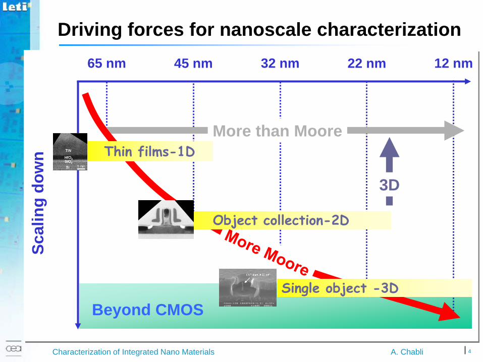
Beyond CMOS
65 nm 45 nm 32 nm 22 nm 12 nm
Scal
ing
dow
n
More than MooreThin films-1D
Object collection-2D
Single object -3D
3D
Driving forces for nanoscale characterization

5
2007
© CEA 2009. All rights reserved Any reproduction in whole or in part on any medium or use of the information contained herein
is prohibited without the prior written consent of CEA
Characterization of Integrated Nano Materials A. Chabli
Outline
A new nanomaterial context Down to 45 nm CMOS technology Below the 45 nm CMOS technology Integration of nanomaterials Conclusion
From the point of view of characterization
6
2007
© CEA 2009. All rights reserved Any reproduction in whole or in part on any medium or use of the information contained herein
is prohibited without the prior written consent of CEA
Characterization of Integrated Nano Materials A. Chabli
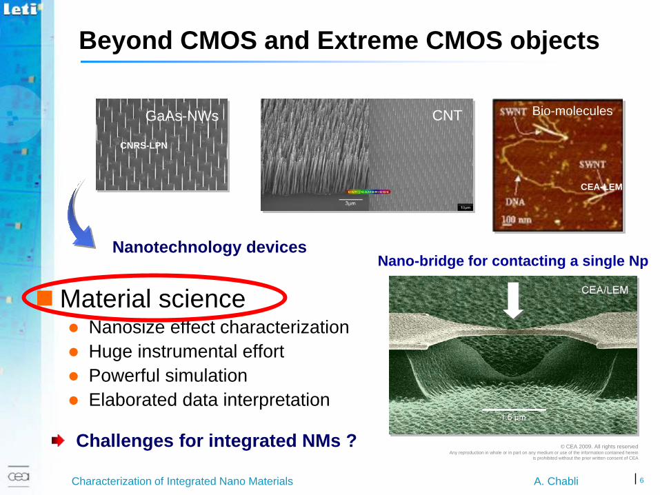
Material science Nanosize effect characterization Huge instrumental effort Powerful simulation Elaborated data interpretation
Beyond CMOS and Extreme CMOS objects
CNTGaAs-NWs Bio-molecules
CNRS-LPN
CEA-LEM
Nanotechnology devices Nano-bridge for contacting a single Np
Challenges for integrated NMs ?
7
2007
© CEA 2009. All rights reserved Any reproduction in whole or in part on any medium or use of the information contained herein
is prohibited without the prior written consent of CEA
Characterization of Integrated Nano Materials A. Chabli
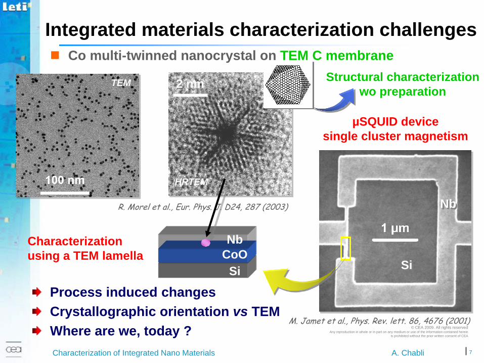
R. Morel et al., Eur. Phys. J. D24, 287 (2003)
µSQUID devicesingle cluster magnetism
Integrated materials characterization challenges
2 nm
HRTEM
Structural characterizationwo preparation
Co multi-twinned nanocrystal on TEM C membrane
Si
Nb
M. Jamet et al., Phys. Rev. lett. 86, 4676 (2001)
Characterization using a TEM lamella
TEM
NbCoO
Si
Process induced changesCrystallographic orientation vs TEMWhere are we, today ?

8
2007
© CEA 2009. All rights reserved Any reproduction in whole or in part on any medium or use of the information contained herein
is prohibited without the prior written consent of CEA
Characterization of Integrated Nano Materials A. Chabli
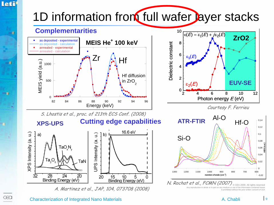
Down to 45 nm node CMOS technology New materials HiK, LoK, Metallic alloys,…
Metal gate stacks, Cu interconnects
Advanced processes ALD, Epitaxy, …
Layer thickness down to the nm Process improvement and control require mainly 1D
information
Representative full wafer layers and stacks of the integrated materials are available
Sub nanometer depth resolution mandatory
Integration Material properties within thin layersInterface stability
Courtesy A.-M. Papon
9
2007
© CEA 2009. All rights reserved Any reproduction in whole or in part on any medium or use of the information contained herein
is prohibited without the prior written consent of CEA
Characterization of Integrated Nano Materials A. Chabli
1D information from full wafer layer stacks
0
500
1000
1500
82 84 86 88 90 92 94 96
MEIS He+ 100 keVas deposited - experimentalas deposited - calculationannealed - experimentalannealed - calculation
Energy (keV)
ME
IS y
ield
(a.u
.) Zr
Hf diffusionin ZrO
2
Hf
S. Lhostis et al., proc. of 213th ECS Conf. (2008)
0
2
4
6
8
10
2 4 6 8 10 12
Die
lect
ric c
onst
ant
Photon energy E (eV)
1 2( ) ( ) ( )E E j Eε = ε + ε
1( )Eε
2( )Eε0
2
4
6
8
10
2 4 6 8 10 12
Die
lect
ric c
onst
ant
Photon energy E (eV)
1 2( ) ( ) ( )E E j Eε = ε + ε
1( )Eε
2( )Eε EUV-SE
ZrO2
Courtesy F. Ferrieu
XPS-UPS
A. Martinez et al., JAP, 104, 073708 (2008)
-0,02
0
0,02
0,04
0,06
0,08
0,1
0,12
0,14
6007008009001000110012001300nombre d'onde (cm-1)
AB
S (u
.a.)
Al2O3
Hf/Al 1:9
Hf/Al 1:6
Hf/Al 1:4
Hf/Al 1:3
Hf/Al 1:2
Hf/Al 9:1
HfO2Si-O
Al-OHf-O
-0,02
0
0,02
0,04
0,06
0,08
0,1
0,12
0,14
6007008009001000110012001300nombre d'onde (cm-1)
AB
S (u
.a.)
Al2O3
Hf/Al 1:9
Hf/Al 1:6
Hf/Al 1:4
Hf/Al 1:3
Hf/Al 1:2
Hf/Al 9:1
HfO2
-0,02
0
0,02
0,04
0,06
0,08
0,1
0,12
0,14
6007008009001000110012001300nombre d'onde (cm-1)
AB
S (u
.a.)
Al2O3
Hf/Al 1:9
Hf/Al 1:6
Hf/Al 1:4
Hf/Al 1:3
Hf/Al 1:2
Hf/Al 9:1
HfO2Si-O
Al-OHf-OATR-FTIR
N. Rochat et al., FCMN (2007)
Complementarities
Cutting edge capabilities
10
2007
© CEA 2009. All rights reserved Any reproduction in whole or in part on any medium or use of the information contained herein
is prohibited without the prior written consent of CEA
Characterization of Integrated Nano Materials A. Chabli
Below 45 nm node CMOS technology Size effect on material properties Cu lines
Local growth (SiGe S/D) Selective epitaxy
Process improvement and control require more and more 2D information
Representative features of integrated materials withonly conservative 3rd dimension are available
Imaging with nanometer spatial resolution required
Integration Size dependent propertiesInduced new phenomena and properties

11
2007
© CEA 2009. All rights reserved Any reproduction in whole or in part on any medium or use of the information contained herein
is prohibited without the prior written consent of CEA
Characterization of Integrated Nano Materials A. Chabli
2D information for specific features
EBSD
KFMW
orkf
unct
ion
(eV)
4.87
4.88
4.89
4.90
N. Gaillard et al., Microelec. Eng. 83 (2006)
J.-P. Barnes et al.SIMS XVI Int. Workshop (2007)
0.4 µm Cu line
3 µm Cu line
Cl10 µm
ClCl10 µm10 µm
CuCuTOF-SIMS
Surface topography
K. Kaja et al. Poster TU-011
Cu interco.
Metal gate
N. Barrett et al.Poster WE-025
5 µm

12
2007
© CEA 2009. All rights reserved Any reproduction in whole or in part on any medium or use of the information contained herein
is prohibited without the prior written consent of CEA
Characterization of Integrated Nano Materials A. Chabli
2D information from electron microscopy
HR-HAADF-STEM
OrientationStrainChemistry
Uppermostspatial resolution
Courtesy M. Jublot
EF-TEM
TiON
GateSource
Drain
GateSource
Drain
Conservative 3rd dimension is required
[110]Si
220
002NBED
2.5 nmspot size
TEM
SiSiO2
SiNSiO2
TiN
Hf02
p-Si
Th. Ernst, this conf., invited
φ-FET structure C. Duprey et al., IEDM (2008)

13
2007
© CEA 2009. All rights reserved Any reproduction in whole or in part on any medium or use of the information contained herein
is prohibited without the prior written consent of CEA
Characterization of Integrated Nano Materials A. Chabli
200 nm200 nm
45 nm CMOS Electron holography
D. Cooper et al.Poster TH-014
D. Cooper et al., APL 93, 183509 (2008)
Si p/n junctions
ImprovedStandard ImprovedStandard
2D information from electron microscopy
Dark field holography
Reference
More about dark field holo.: M. Hitch, this conf., invited
Courtesy D. CooperCourtesy D. Cooper
Conservative 3rd dimension is required
14
2007
© CEA 2009. All rights reserved Any reproduction in whole or in part on any medium or use of the information contained herein
is prohibited without the prior written consent of CEA
Characterization of Integrated Nano Materials A. Chabli
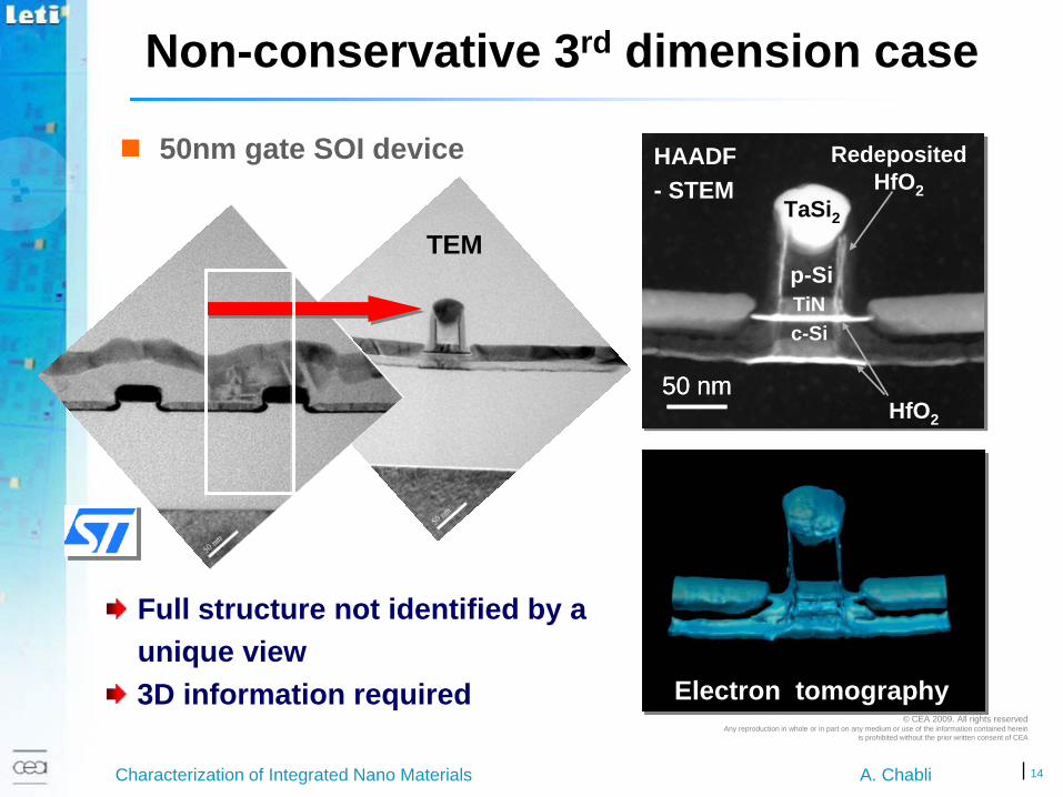
TEM
Non-conservative 3rd dimension case
50nm gate SOI device
Full structure not identified by a unique view
TaSi2
TiN
HfO2
p-Si
RedepositedHfO2
c-Si
50 nm
TaSi2
TiN
HfO2
p-Si
RedepositedHfO2
c-Si
50 nm50 nm
HAADF- STEM
Electron tomography3D information required
15
2007
© CEA 2009. All rights reserved Any reproduction in whole or in part on any medium or use of the information contained herein
is prohibited without the prior written consent of CEA
Characterization of Integrated Nano Materials A. Chabli
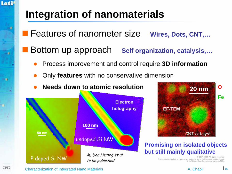
Integration of nanomaterials
Features of nanometer size Wires, Dots, CNT,…
Bottom up approach Self organization, catalysis,…
Process improvement and control require 3D information
Only features with no conservative dimension
Needs down to atomic resolution
50 nm50 nm50 nm
P doped Si NWM. Den Hertog et al.,to be published
100 nm100 nm100 nm
undoped Si NW
Electronholography
20 nm20 nm20 nm20 nm20 nm20 nmFe
O
CNT catalyst
20 nm20 nm20 nm20 nm20 nm20 nmFe
O20 nm20 nm20 nm20 nm20 nm20 nmFe
O
CNT catalyst
EF-TEM
Promising on isolated objects but still mainly qualitative

16
2007
© CEA 2009. All rights reserved Any reproduction in whole or in part on any medium or use of the information contained herein
is prohibited without the prior written consent of CEA
Characterization of Integrated Nano Materials A. Chabli
Beyond CMOS nanomaterial integration
1,2 µm
Electrical Scanning Probe Microscopy
AFM
VAC = 1VVDC = 0V50 kHz
VAC = 1VVDC = 0V50 kHz
SCM
VAC = 1VVDC = 0V50 kHz
VAC = 1VVDC = 0V50 kHz
SCM
Vertical ZnO NWs embedded in polymer
E. Latu-Romain & al., EMRS (2008)
2 µm2 µm
1013
109
300 nm
R (Ω
)
SSRM1013
109
300 nm
R (Ω
)
1013
109
300 nm300 nm
R (Ω
)
SSRMSSRM1013
109
300 nm
R (Ω
)
SSRM1013
109
300 nm
R (Ω
)
1013
109
300 nm300 nm
R (Ω
)
SSRMSSRM
Properties modification
N. Chevalier et al. Poster TH-020
SEM
300nm
17
2007
© CEA 2009. All rights reserved Any reproduction in whole or in part on any medium or use of the information contained herein
is prohibited without the prior written consent of CEA
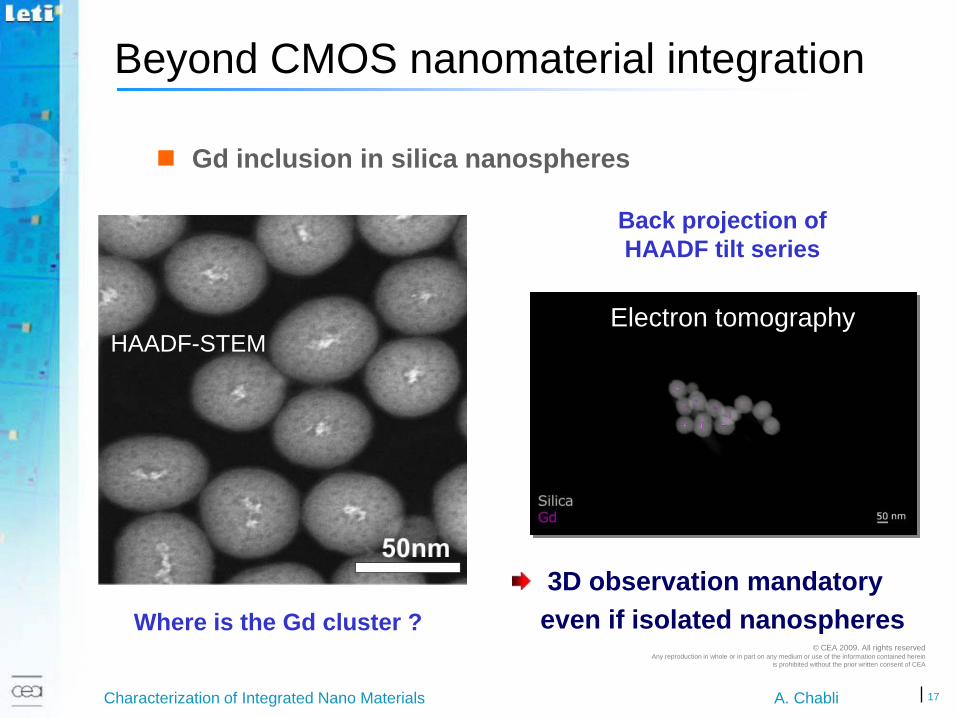
Characterization of Integrated Nano Materials A. Chabli
Beyond CMOS nanomaterial integration
3D observation mandatory even if isolated nanospheres
HAADF-STEM
Gd inclusion in silica nanospheres
Electron tomography
Where is the Gd cluster ?
Back projection of HAADF tilt series

18
2007
© CEA 2009. All rights reserved Any reproduction in whole or in part on any medium or use of the information contained herein
is prohibited without the prior written consent of CEA
Characterization of Integrated Nano Materials A. Chabli
Th. Ernst, this conf., invited
Thickness changes with tiltShadowing at high angle
Gate-all-around (GAA) transistors
2 µm2 µm2 µm
100-200nm thickParallel-sided lamella
3D for top down approach extreme CMOS
Conventional preparation
19
2007
© CEA 2009. All rights reserved Any reproduction in whole or in part on any medium or use of the information contained herein
is prohibited without the prior written consent of CEA
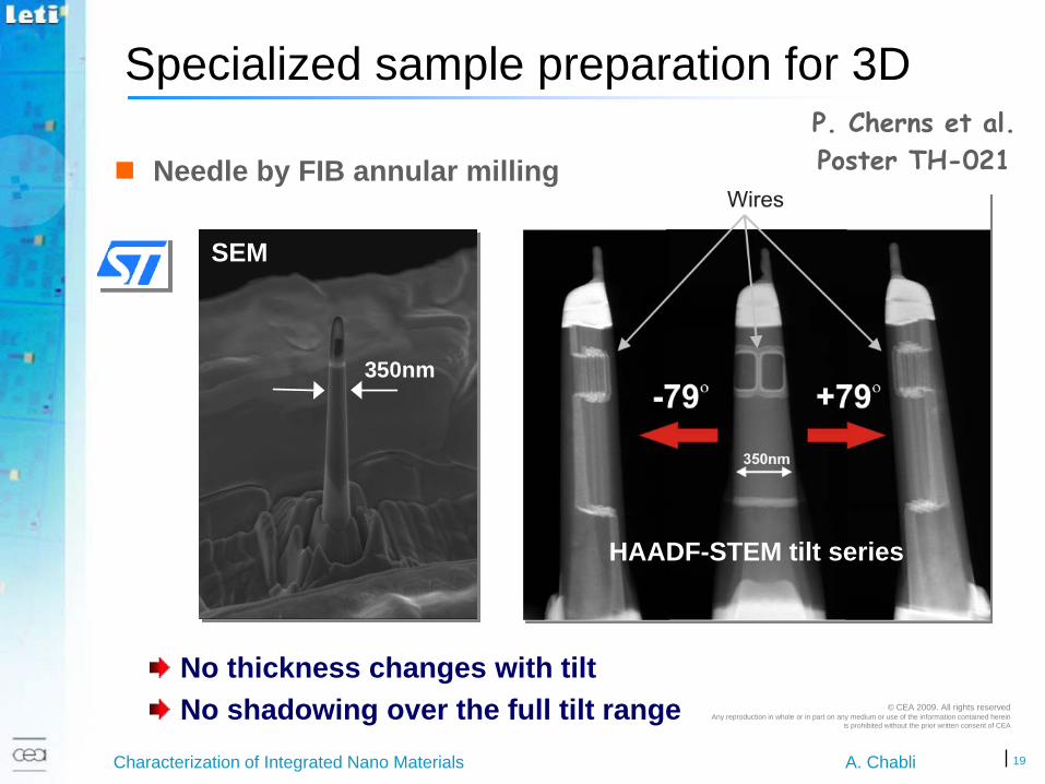
Characterization of Integrated Nano Materials A. Chabli
No thickness changes with tiltNo shadowing over the full tilt range
P. Cherns et al.Poster TH-021
Specialized sample preparation for 3D
HAADF-STEM tilt series
Needle by FIB annular milling
350nm350nm
SEM
20
2007
© CEA 2009. All rights reserved Any reproduction in whole or in part on any medium or use of the information contained herein
is prohibited without the prior written consent of CEA
Characterization of Integrated Nano Materials A. Chabli
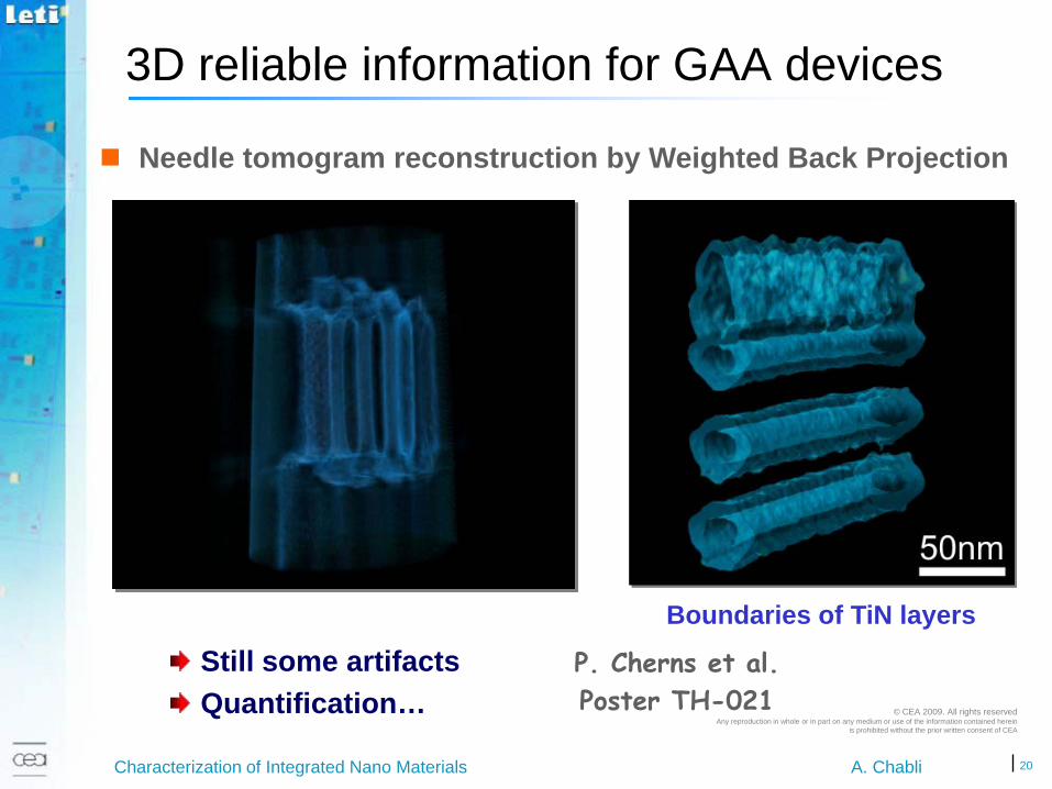
3D reliable information for GAA devices
Needle tomogram reconstruction by Weighted Back Projection
Still some artifactsQuantification…
P. Cherns et al.Poster TH-021
Boundaries of TiN layers

21
2007
© CEA 2009. All rights reserved Any reproduction in whole or in part on any medium or use of the information contained herein
is prohibited without the prior written consent of CEA
Characterization of Integrated Nano Materials A. Chabli
Beyond CMOS
65 nm 45 nm 32 nm 22 nm 12 nm
Scal
ing
dow
n
More than MooreThin films-1D
Object collection-2D
Single object -3D
Support
ProtocolsRelevance
Frontier
3D
Challenges in nanoscale characterization
22
2007
© CEA 2009. All rights reserved Any reproduction in whole or in part on any medium or use of the information contained herein
is prohibited without the prior written consent of CEA
Characterization of Integrated Nano Materials A. Chabli
Aknowledgments
A. Bailly J.-P. Barnes N. Barrett F. Bertin N. Bernier N. Bicaïs P. Bleuet A. Brenac P. Cherns N. Chevalier
W. Li Ling M. Lavayssière Ch. Licitra D. Mariolle E. Martinez A.-M. Papon F. Pierre O. Renault N. Rochat J.-L. Rouvière R. Truche …
D. Cooper H. Dansas Th. Ernst F. Ferrieu F. Fillot P. Gergaud J.-M. Hartmann M. Jublot K. Kaja D. Lafond E. Latu-Romain
23
2007
© CEA 2009. All rights reserved Any reproduction in whole or in part on any medium or use of the information contained herein
is prohibited without the prior written consent of CEA
Characterization of Integrated Nano Materials A. Chabli
For more information www.leti.fr
Join us for the
11th Leti Annual Review
June 22-23, 2009at Minatec
24
2007
© CEA 2009. All rights reserved Any reproduction in whole or in part on any medium or use of the information contained herein
is prohibited without the prior written consent of CEA
Characterization of Integrated Nano Materials A. Chabli
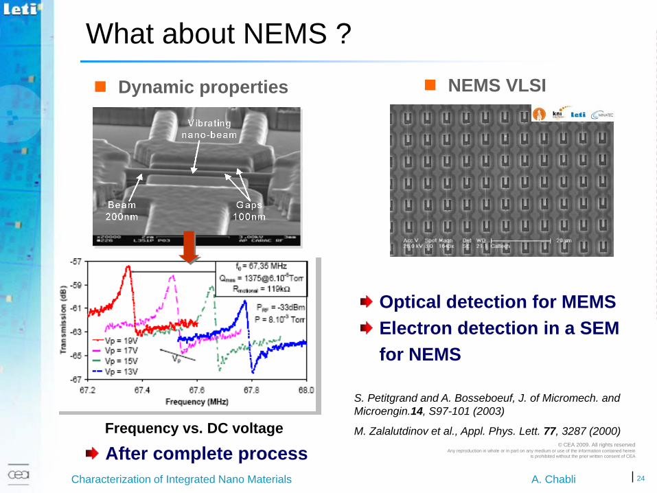
Frequency vs. DC voltage
What about NEMS ?
After complete process
Dynamic properties NEMS VLSI
Optical detection for MEMSElectron detection in a SEM for NEMS
M. Zalalutdinov et al., Appl. Phys. Lett. 77, 3287 (2000)
S. Petitgrand and A. Bosseboeuf, J. of Micromech. and Microengin.14, S97-101 (2003)