characterization of contamination in pv materials · characterization of contamination in pv...
TRANSCRIPT

Characterization of Contamination in PV Materials
Ian Mowat, Karol Putyera, Larry Wang,Temel Buyuklimanli and Gary Mount
810 Kifer Road, Sunnyvale, CA 94086
www.eaglabs.com

© Copyright 2011 Evans Analytical Group LLC 2
Summary
• Intro to EAG• Contamination in PV materials• Analytical methods
– ICPMS, GDMS, SIMS
• c-Si• Thin film
– a-Si– CdTe– CIGS
• Conclusions

© Copyright 2011 Evans Analytical Group LLC 3
Who is Evans Analytical Group?
• Established in 1978• 15 locations in 8 countries• 30+ analytical techniques
• Origins in semiconductor industry support• Very active in PV sector for many years
– We have developed considerable expertise in measurement of contamination

© Copyright 2011 Evans Analytical Group LLC 4
Contamination in Solar PV
• All solar technologies can be improvedwith contamination control.
• Each solar technology has different issues anddifferent contaminants that are important.
• Some elements have known effects.• Other elements little known effect.• Some cell designs are more sensitive than
others to the same elements.• To be useful: measurements need to be ACCURATE.• To be useful: measurements need to be
REPRODUCIBLE.

© Copyright 2011 Evans Analytical Group LLC 5
Sampling and Measurement Issues
• Is sampling representative?• Does the sampling method change
the sample?• Understand WHAT is being measured.
– Inside/interior of sample?– Outside/exterior of sample?– Both?
• Understand the analytical method.

© Copyright 2011 Evans Analytical Group LLC 6
Inductively Coupled Plasma Mass Spectrometry
Plasma Torch
Mass SpectrometerSample
Preparation

© Copyright 2011 Evans Analytical Group LLC 7
ICPMS
• Survey analysis technique.• PPM to PPB detection limits, depending on element.• Relatively large sample size.• Measures whole sample both interior and exterior.• Does not measure ‘atmospheric’ elements.• P, an important dopant, can be difficult.• Solid samples must be dissolved completely prior to
analysis.• Sample prep potentially vulnerable to added
contamination.

© Copyright 2011 Evans Analytical Group LLC 8
Glow Discharge Mass Spectrometry
* *

© Copyright 2011 Evans Analytical Group LLC 9
GDMS
• Survey analysis technique• PPM to PPB detection limits depending on element.• Sample does NOT need to be dissolved.• Direct sampling of all forms of solid PV materials.• Sample prep contamination rarely an issue.• SEMI Standard Test Method for PV Si (SEMI PV1-0309)• Smaller sample size than ICPMS• Measures mostly the sample interior.• Does not measure ‘atmospheric’ elements.

© Copyright 2011 Evans Analytical Group LLC 10
Secondary Ion Mass Spectrometry
Extraction

© Copyright 2011 Evans Analytical Group LLC 11
SIMS
• PPM to PPT detection limits depending on element.• Does measure ‘atmospheric’ elements H,C,N,O.• Sample does NOT need to be dissolved.• Sample prep contamination is generally not an issue.• Direct sampling of all forms of solid PV materials.• Generally measures the sample interior.• Smaller sample size than GDMS.• A few elements at one time.

c-Si
e-Grade / UMG / Solar Grade
© Copyright 2011 Evans Analytical Group LLC 13
c-Si
Silicon feedstocks• A few years ago polysilicon was in short supply
and very expensive.• Solar cell makers resorted to using relatively
low grade silicon - anything they could find• Many new polysilicon producers have since come
online, many with the goal of producing low costhigh purity silicon using Siemens or ‘Modified’Siemens process.

© Copyright 2011 Evans Analytical Group LLC 14
Contamination in Solar PV
• There are no standards that say whatcontaminants and what levels are acceptable
• Without standards materials for PVapplications are described in terms of ‘nines’or ‘N’s (example: 99.99999% pure or 7 nines)
• Number of ‘N’s does not discriminate betweenelements that are important and those thatare not.
• Number of ‘N’s excludes elements themeasuring technique cannot measure!– Number of ‘N’s typically excludes atmospheric
elements.

© Copyright 2011 Evans Analytical Group LLC 15
A typical bulk SIMS analysis of PV Si grown by Siemens Process
SIMS Bulk Analysis results Detection limitsElements Conc.(at/cm3) Conc.(ppbat) Conc.(ppbwt) Conc.(at/cm3)
B 4.9E+13 0.98 0.38 5E+12Na <4.0E+11 <0.008 <0.006 4E+11Al <6.0E+12 <0.12 <0.1 6E+12P 7.2E+13 1.44 1.59 5E+12Cr <3.0E+11 <0.006 <0.01 3E+11Fe <1.0E+13 <0.20 <0.4 1E+13Ni <1.0E+14 <2.00 <4 1E+14Cu <1.0E+14 <2.00 <4 1E+14Zn <2.0E+14 <4.00 <9 2E+14K <4.0E+11 <0.01 <0.01 4E+11C <3.0E+15 <60 <25 3E+15As 8.4E+13 1.68 4.54 5E+12Sb 7.8E+13 1.56 6.76 1E+13
• Silicon has 7N purity considering all listed elements
• Silicon has 8N purity if we exclude carbon

© Copyright 2011 Evans Analytical Group LLC 16
Contamination in Solar PV
• Materials specifications based on ‘N’smake it necessary to reduce contaminantsthat are not important for PV performance.
• Materials based on ‘N’s may be moreexpensive than they need to be.
• Rather than reducing all contaminantsindiscriminately, wouldn’t it make senseto focus on the most important for PVperformance?

© Copyright 2011 Evans Analytical Group LLC 17
Semi Committee on Solar Grade Silicon
Four grades of ‘Solar Grade Silicon’ are proposed with Specifications for:
1. Acceptors: B, Al
2. Donors: P, As, Sb
3. Transition and Post Transition Metals: Ti, Cr, Fe, Ni, Cu, Zn, Mo
4. Alkali and Earth Alkali Metals: Na, K, Ca
5. Atmospherics: H, C, O, Cl
• Proposed specifications do not mention ‘nines’ or ‘N’s anywhere.
• Specifications related to the performance of PV cells.

© Copyright 2011 Evans Analytical Group LLC 18
Proposed Solar Grades
Grade I II III IV
Acceptors < 2 ppba < 20 ppba < 300 ppba < 1000 ppba
Donors < 2 ppba < 20 ppba < 50 ppba < 750 ppba
Total Al - - - < 1000 ppba
Bulk O Not specified Not specified Not specified Not specified
C < 0.5 ppma < 2 ppma < 5 ppma < 100 ppma
Transition Metals < 10 ppba < 50 ppba < 100 ppba < 200 ppba
Alkali and Earth Alkali < 10 ppba < 50 ppba < 100 ppba < 4000 ppba
• Proposal will be balloted in March 2011

© Copyright 2011 Evans Analytical Group LLC 19
UMG-Si
Upgraded Metallurgical Grade Feedstock• Recently it appeared UMG silicon would not
have a place vs. low cost Siemens process.• Futher improvements in UMG quality and its
inherent low costs have given it new life.• Siemens process silicon: $50/kg• UMG $15/kg – BUT need to know exactly what
contaminants are present and how to handle them.

© Copyright 2011 Evans Analytical Group LLC 20
[B], [P], [C] and [O] by SIMS
• Low cost solar requires low cost analyses.• A more cost effective ‘all-in-one’ SIMS
measurement was developed for B, P, C and O.
Protocol B C O P
B,C,O,P together 1e14 2e16 5e16 2e14
• Detection limits will be sufficient for Si solar wafers and UMG-Si.
• Measurement can be made on thin Si solar wafers or Si chunks/pieces.
• Precision should be sufficient (15-20%, 3 sigma).• Proposed Semi Test Method in ballot.

© Copyright 2011 Evans Analytical Group LLC 21
Comparing Test Methods
SIMS GDMS
B 1.1 0.8
C 9 -
O 30 -
Al 0.3 0.4
P 8.1 11.4
Cr <7E-5 <0.01
Fe <0.001 1.3
Ni <0.008 <0.01
As 0.07 -
• Test results from different methods often show different results.• Fe shows great differences, why?

© Copyright 2011 Evans Analytical Group LLC 22
SIMS Profile on Granule
0 5 10 15DEPTH (microns)
10 13
10 14
10 15
10 16
10 17
10 18
10 19
10 20
CO
NC
EN
TRA
TIO
N (a
tom
s/cc
)
Fe
0-4 um Fe: 2.73E16 at/cm3
Fe(>12 um) <3E13 at/cm3
• GDMS measures both inside and outside the particles and some Fe surface contamination will be included.
• SIMS bulk measurement excludes the surface contamination.
α-Si
α-Si / µc-Si
© Copyright 2011 Evans Analytical Group LLC 24
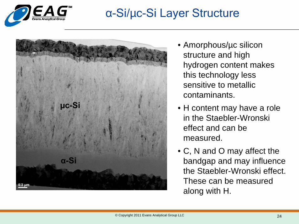
α-Si/µc-Si Layer Structure
• Amorphous/µc silicon structure and high hydrogen content makes this technology less sensitive to metallic contaminants.
• H content may have a role in the Staebler-Wronski effect and can be measured.
• C, N and O may affect the bandgap and may influence the Staebler-Wronski effect. These can be measured along with H.
µc-Si
α-Si

© Copyright 2011 Evans Analytical Group LLC 25
H and Contaminants in α-Si by SIMS
SIMS
0 1000 2000 3000 4000 5000 6000 7000 8000Depth (A)
10 16
10 17
10 18
10 19
10 20
10 21
10 22
10 23
Con
cent
ratio
n (A
tom
s/cm
3)
100
101
102
103
104
105
106
Sec
onda
ry io
n in
tens
ity (c
ount
s/se
c)
C
O
H
F
Si(Counts)
N
α-Si glass

CdTe

© Copyright 2011 Evans Analytical Group LLC 27
CdTe Layer Structure
CdTe
CdS
SnO
• There are no agreed upon standards for acceptable amounts of contaminants in CdTe
• Each company has their own specifications for contamination.
• Copper helps to make improved back contact and is expected through the CdTe film.
© Copyright 2011 Evans Analytical Group LLC 28
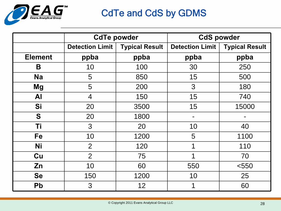
CdTe and CdS by GDMS
CdTe powder CdS powderDetection Limit Typical Result Detection Limit Typical Result
Element ppba ppba ppba ppbaB 10 100 30 250Na 5 850 15 500Mg 5 200 3 180Al 4 150 15 740Si 20 3500 15 15000S 20 1800 - -Ti 3 20 10 40Fe 10 1200 5 1100Ni 2 120 1 110Cu 2 75 1 70Zn 10 60 550 <550Se 150 1200 10 25Pb 3 12 1 60

© Copyright 2011 Evans Analytical Group LLC 29
Metal Contaminants in CdTe/CdS/SnO by SIMS
0 1 2 3 4 5Depth (um)
10 14
10 15
10 16
10 17
10 18
10 19
10 20
10 21C
once
ntra
tion
(Ato
ms/
cm3)
10-1
100
101
102
103
104
105
106
Sec
onda
ry io
n in
tens
ity (c
ount
s/se
c)
Fe
Ni
Zn
S(raw ion counts)→
Cd(raw ion counts)→
Te(raw ion counts)→
Cu
CdTeCdS
SnO glass

Cux(InyGa(1-y))(1-x)Se2 (CIGS)
© Copyright 2011 Evans Analytical Group LLC
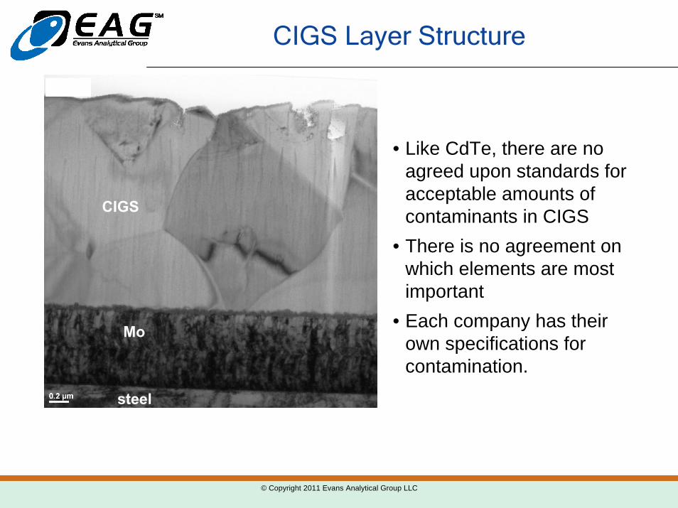
CIGS Layer Structure
• Like CdTe, there are no agreed upon standards for acceptable amounts of contaminants in CIGS
• There is no agreement on which elements are most important
• Each company has their own specifications for contamination.
CIGS
Mo
steel

© Copyright 2011 Evans Analytical Group LLC 32
Analysis of CuInGa by GDMS
72 elements in one measurement, most with 1ppb detection limit

© Copyright 2011 Evans Analytical Group LLC 33
Metal Contaminants in CIGS by SIMS
• Fe, Ni, Cr and Al are generally considered ‘important’• Detection limit of 0.1-0.01 ppm for ‘all together’ measurement
0 0.5 1 1.5 2
Depth (um)
10 14
10 15
10 16
10 17
10 18
10 19
10 20
10 21C
once
ntra
tion
(Ato
ms/
cm3)
AlCr
Fe
Ni
Mo→
In→ CIGS
100
101
102
103
104
105
106
107
108
Sec
onda
ry io
n in
tens
ity (C
ount
s/se
c)
Mo

Conclusions
• Measure what matters
• Measure appropriately
• Full understanding of contaminant effects requires a detailed investigation of process steps
• Relating contaminant levels to performance is possible
© Copyright 2011 Evans Analytical Group LLC 34

End