characterization of coated conductors in the ultra-high ... ·...
TRANSCRIPT

Characteriza*on of coated conductors in the ultra-‐high field regime.
Plan
1. Mo*va*on
2. Prepara*on ultra narrow bridges 3. Setup for measuring for ultra fast I-‐V measurements in pulsed magne*c fields
4. Tes*ng bridges: Ic(T, SF) and R(T,B) 5. Measuring V(I,B,T) curves in pulsed fields up to 65T
6. Calcula*on of Ic from V(I,B) dependencies
7. Summary
8. Future plans
D. Abraimov1, F. F. Balakirev2, and D.C. Larbales9er1 1ASC, NHMFL, Tallahassee 2NHMFL Pulsed Field Facility, Los Alamos Na9onal Laboratory
SuperPower Inc. 7.5% and 15% Zr doped tapes produced for CORC applica9on were used for Ic measurements
This work was supported in part by the U.S. Na9onal Science Founda9on under Grant No. DMR-‐1157490 and the State of Florida.

Mo*va*on
• ReBCO superconductors become a choice material for developing all
superconduc*ng magnets capable genera*ng ultra-‐high fields due to very high
cri*cal current densi*es in the presence of magne*c fields and high irreversibility
fields
• Therefore, it is important to develop instrumenta*on suitable for tes*ng Ic , Jc, fp
of ReBCO conductors in such regime
• Recent progress in introducing high concentra*on ar*ficial pinning centers (APC)
in ReBCO conductors makes them op*mized for low-‐temperature high-‐field
applica*ons
• The understanding performance of APC at ultra-‐high fields is fascina*ng vortex
dynamics problem and important applica*on task
• For now pulsed magnets is the only available choice for genera*ng fields above
45T

Manufacturer Material α at BIIc α at 18 o
SuperPower ReBCO 0.67-‐0.76 0.7-‐0.9
SuNAM ReBCO 0.6; 0.6 0.69; 0.68
SuperOx ReBCO 0.54; 0.54 0.588; 0.59
Fujikura ReBCO 0.641; 0.69 0.70
AMSC ReBCO 0.74
Bruker ReBCO 0.88-‐0.89
𝐼↓𝑐 ~ 𝐵↑−𝛼
Tapes from different manufacturers have different slope α
Transport Ic(B,4K) were measured by D. Abraimov, A. Fransis, M. Santos, and J. Jaroszynski

10 1001
10
Uni Houston 15% Zr; 0.9 µm ReBCO Bruker T190D-C SN1; 2 µm ReBCO Bruker T190D-C SN2; 2 µm ReBCO SP215; 7.5% Zr; (2X50 µm Cu); ~1.55 µm ReBCO Uni Houston 7.5% Zr; 0.9 µm ReBCO SP 15% Zr; 1.52 µm ReBCO; W=4mm (2x5µm Cu) SP26; 840 um bridge; 7.5% Zr; 1um ReBCO
J c(B,4
.2K
), M
A/c
m2
B, T
Comparison Jc from different ReBCO samples (0.9um – 2um thick)
Uni Houston data taken from : <<Strongly enhanced vortex pinning in a broad temperature and magne*c field range of Zr-‐added MOCVD coated conductors>> Aixia Xu, et al. Mo*va*on
Transport Ic(B,4K) were measured by D. Abraimov, Aixia Xu, J. Jaroszynski

20 30 40 50 60 70 80 90 1001
2
3
4
5
6
789
10
Uni Houston 15% Zr; 0.9 µm ReBCO Bruker T190D-C SN1; 2 µm ReBCO Bruker T190D-C SN2; 2 µm ReBCO SP215; 7.5% Zr; (2X50 µm Cu); ~1.55 µm ReBCO Uni Houston 7.5% Zr; 0.9 µm ReBCO SP 15% Zr; 1.52 µm ReBCO; W=4mm (2x5µm Cu) SP26; 840 um bridge; 7.5% Zr; 1um ReBCO
J c(B,4
.2K
), M
A/c
m2
B, T
Can we trust extrapola*ons?
Uni Houston data taken from : <<Strongly enhanced vortex pinning in a broad temperature and magne*c field range of Zr-‐added MOCVD coated conductors>> Aixia Xu, et al. Mo*va*on
Transport Ic(B,4K) were measured by D. Abraimov, Aixia Xu, J. Jaroszynski

Project
SP
machine
ReBCO
thickness, µm
Zr
doping, %
Substrate
thickn
ess, µm
Cu layer thickness,
µm
α
<Ic(15T, 4K)>, A
Je(15T,4K), kA/cm2
32T M3 0.9-‐1 7.5 50 2x50 0.746 j 183 j 45.5 j 32T M4 1.5-‐1.6 7.5 50 2x50 0.776* 283* 70.4*
CORC® M3 ≈1 7.5 38 2x5 0.754 241 108 CORC® M4 ≈1.5-‐1.6 7.5 30 2x5 0.77 302 164 CORC® M4 ≈1.5-‐1.6 15 50 2x5 0.864 320 117
* Average out of 15 representa*ve tapes j Average out of 12 representa*ve tapes
Different tape architecture for magnet and cable applica*ons In-‐field transport proper*es at 4K, BIIc orienta*on for SuperPower Inc. 4 mm wide tapes
The first two rows are representa*ve M3 and M4 tapes purchased for 32T magnet project. Other rows were tested for CORC® project.
Slightly lower α values for M3 tapes suggest that those tapes may have smaller Zr doping, than M4 tapes. Tapes with nominal 15% Zr doping have larger α, but not as high, as for tapes produced in Houston Uni. lab.
Ic~B –α
Transport Ic(B,4K) were measured by D. Abraimov, A. Francis, M. Santos, and J. Jaroszynski

1 10200
400
600
800
1000
12001400160018002000
Un i Ho usto n 1 5% Z r; 0.9 µm R eBCO Br uke r T19 0D- C SN1 ; 2 µm Re BCO Br uke r T19 0D- C SN2 ; 2 µm Re BCO SP21 5; 7.5 % Z r; ( 2X5 0 µm C u); ~1 .55 µm R eBCO Un i Ho usto n 7 .5% Zr ; 0. 9 µm ReBCO SP 1 5% Z r; 1.5 2 µm ReBCO ; W= 4m m (2 x5µm Cu) SP26 ; 8 40 um br idg e; 7.5 % Zr ; 1 um ReBC O
f pin(
B, B
IIc, 4
.2K
), G
N/m
3
B, T
What is shape of pinning force density at higher fields?
SP 15% Zr
SP215 7.5%
Zr
Mo*va*on
4.2 K, B⊥ tape
Transport Ic(B,4K) were measured by D. Abraimov, Aixia Xu, J. Jaroszynski

1. Technical: find procedure of measuring Ic(B,T,θ) in pulsed field up to 65T
for commercially available high Jc ReBCO;
2. For magnet applica*on:
• Transport current property -‐ explore Ic limi*ng factors at cri*cal
magne*c field orienta*ons – near 18o-‐20o;
• Transport current and mechanical property -‐ find experimentally
maximum in field shear stress for ReBCO layer in B_|_ tape
orienta*on;
3. Physics/Material science and assistance to tape manufacturers:
calculate and compare vortex pinning force dependence fp(B, T) for two
SuperPower Inc. tapes containing different Zr doping: 7.5% and 15%;
Purposes of this experiment

Major problems: 1. High induc*on voltages in the sample, 2. The very limited *meframe to
• ramp current, • detect voltage, • compare it with defined threshold, and • decide to stop current ramp just above Ic.;
3. Possible Joule hea*ng in the sample due to induced eddy currents;
4. Forces on the sample and leads due to magne*c interac*on with the applied field.
Since pulse dura*ons are <0.1 sec., measurements of high Ic are a tough technical task.
• To compare the effect of different BZO pinning concentra*ons we used
SuperPower Inc. tapes with 7.5% Zr and 15% Zr doping
• Tapes with 30 µm, 38 µm, and 50 µm thick substrates and 5 µm thick Cu
layer were used
• Two stage photolithography process was used to paoern 4mm x 4mm
samples.
• We used chemical etching to remove Cu, Ag, and ReBCO
• To get uniform width and reduce Ic all bridges were subsequently trimmed
with a focused ion beam (FIB)
• Using NHMFL facili*es we prepared 14 bridges ranging 47µm-‐ 7.7µm in
length and 4.8µm – 0.49µm in width.
Sample prepara*on for Ic measurements in ultra-‐high magne*c fields
Ultra-‐narrow bridges

Sample: 4X4 mm; Bridge: 50 um X 200 um Current pads: 820 um X 830 um
Mask paoern
Sample prepara*on
Used photolithography to paoern structures
Used chemical etching
Bridges were trimmed with focused ion beam in SEM

SEM image of bridge N13 7.5% Zr doped ReBCO SuperPower I.D. M4-‐337-‐2 0709
a-‐axis grains
ReBCO
FIB trimmed bridge
Buffer
Hastelloy substrate
For ultra narrow bridges we choose region free from a-‐axis grains and CuO par*cles
Sample prepara*on

W= 577 nm L= 12.4 µm t= 1.5 µm (ReBCO thickness)
Thanks to Bob Goddard and Fumetake Kametani we have very negligible stage driV and therefore can make rou*nely bridges about ~0.5µm wide and about 8 µm long
SEM image of bridge N13

SEM image of bridge N10

SEM image of bridge N10

• To prevent overhea*ng and genera*ng forces/torques due magne*za*on currents minimize volumes of conduc*ve materials in sample;
• To avoid using massive current leads reduce criXcal current values by reducing bridge cross sec*on;
• To prevent breaking a bridge by Lorentz force choose sample orienta*on in which Lorentz force is directed toward substrate;
• To avert large Eddy currents in current and voltage leads use twisted pairs with a small pitch. Place connec*ons between probe leads and sample leads away from field center.
• To avoid voltage and bias current noise fix voltage and current leads to probe;
Probe for measuring in pulsed magnet
Sample
Heater
Pick-‐up coil Cernox Sapphire holder
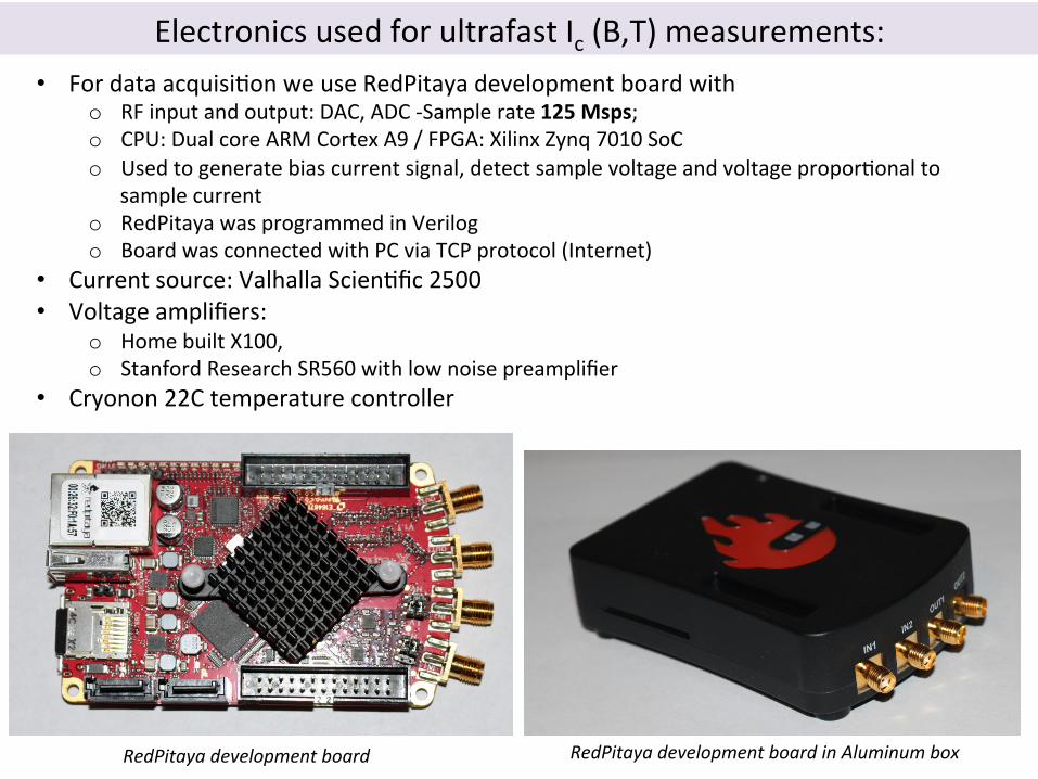
• For data acquisi*on we use RedPitaya development board with o RF input and output: DAC, ADC -‐Sample rate 125 Msps; o CPU: Dual core ARM Cortex A9 / FPGA: Xilinx Zynq 7010 SoC o Used to generate bias current signal, detect sample voltage and voltage propor*onal to
sample current o RedPitaya was programmed in Verilog o Board was connected with PC via TCP protocol (Internet)
• Current source: Valhalla Scien*fic 2500 • Voltage amplifiers:
o Home built X100, o Stanford Research SR560 with low noise preamplifier
• Cryonon 22C temperature controller
Electronics used for ultrafast Ic (B,T) measurements:
RedPitaya development board RedPitaya development board in Aluminum box

0 5 10 15 20 25 30 35 40 45 500
1
2
3
4
5
6
1
2
34
5
678
910
11 121314
W, µ
m
L, µm
Width and length of FIB trimmed ReBCO bridges
SuperPower 15% Zr doped tapes

1010
100
1000
BN1 3.3um Ic (mA) BN2 4.8um Ic (mA) BN3 2.1um Ic (mA) BN4 1.9um Ic (mA) BN5 2.48um Ic (mA) BN6 1.21um Ic (mA) BN7 1.2um Ic (mA) BN8 1.44um Ic (mA) BN9 0.76um Ic (mA) BN10 0.49um Ic (mA) BN11 0.697um Ic (mA) BN12 0.66um Ic (mA) BN13 0.577um Ic (mA) BN14 0.77um Ic (mA)
Ic measured in 15T SC magnet rescaled from full width tape to bridge widthI c(4
K, B
), m
A
B, T
20 30 40 50 60
B perpendicular to tape orientatrion
We need to measure currents up to 10 mA -‐ 200 mA
Es*ma*on of bias current values by extrapola*on
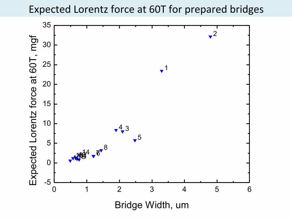
0 1 2 3 4 5 6-5
0
5
10
15
20
25
30
35
1
2
345
678
91011121314
Exp
ecte
d Lo
rent
z fo
rce
at 6
0T, m
gf
Bridge Width, um
Expected Lorentz force at 60T for prepared bridges

Geometry of FIB trimmed ReBCO bridges from SuperPower tapes and es*mated transport /mechanical proper*es
76 77 78 79 80 81 82 83 84 85
30
40
50
60
70
80
90
100
0123
567
8910
11121314
151617
18192021
I c(0T)
at <
E>=
10 µ
V/c
m, m
A
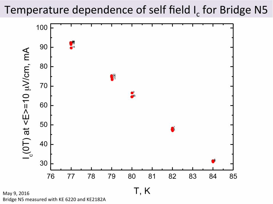
T, KMay 9, 2016 Bridge N5 measured with KE 6220 and KE2182A
Temperature dependence of self field Ic for Bridge N5
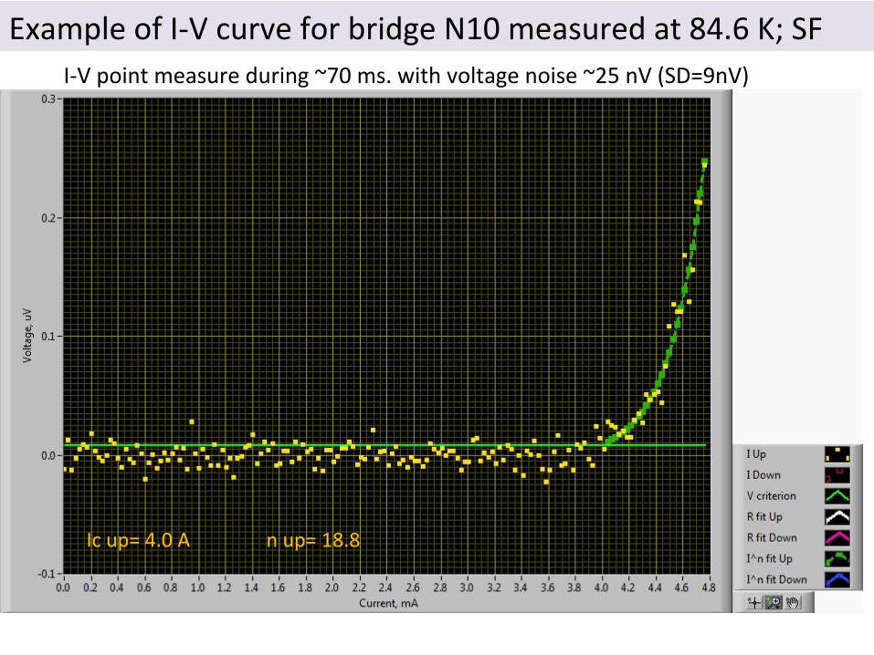
Ic up= 4.0 A n up= 18.8
Example of I-‐V curve for bridge N10 measured at 84.6 K; SF I-‐V point measure during ~70 ms. with voltage noise ~25 nV (SD=9nV)

-5 0 5 10 15 20 25 30 35 40 45 50 55 60 65 70-0.001
0.000
0.001
0.002
0.003
0.004
0.005
0.006
0.007 85 K 82.991 K 81K 79 K 77K 75T 73 K 71K 69 K 67 K 65 K 63 K 61 K 59 K 57 K
R, a
.u.
B, T
R(B,T) measured in pulsed magnet -‐ bridge N5
33.6o to magne*c field; maximum Lorentz force orienta*on

55 60 65 70 75 80 850
10
20
30
40
50
60
µ oHirr,
T
T, K
Hirr(T) measured in pulsed magnet -‐ bridge N5
33.6o to magne*c field; maximum Lorentz force orienta*on
0 10 20 30 40 50 60 70 800
10
20
30
40
50
60
70
80
90
100
110
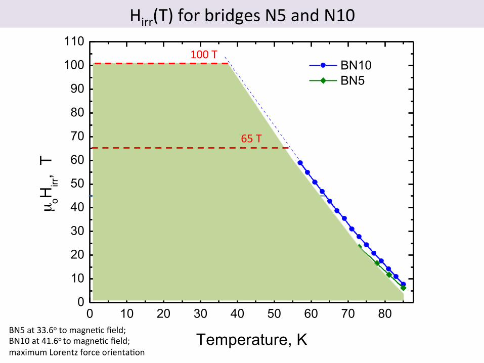
BN10 BN5
µ oHirr,
T
Temperature, K
Hirr(T) for bridges N5 and N10
65 T
100 T
BN5 at 33.6o to magne*c field; BN10 at 41.6o to magne*c field; maximum Lorentz force orienta*on

Example of *me dependencies of magne*c field, bias current and sample voltage for bridge N10 at 52K
Current step 200 µA
41.6 deg. to magne*c field; maximum Lorentz force orienta*on
Voltage trace values are calculated by FPGA algorithm at the end of each current pulse as a difference between current on and current off por*ons of the pulse.

Time dependencies of magne*c field, bias current and sample voltage for bridge N10 at 30K
Current step 200 µA
Dura*on of this process 36 ms. 41.6 deg. to magne*c field; maximum Lorentz force
We detected one V-‐I-‐B point in about 0.33 ms. with voltage noise reaching up to about 2-‐3 µV. Field values were sampled at rate 2 µs. per point.

49.0
49.1
49.2
49.3
49.4
49.5
49.6
-3.2
0.0
3.2
6.4
9.6
0
130
2 6 0
3 9 0
5 2 0
6 5 0
7 8 0
Voltage, µV
Current, µA
B (T)
Example of V(I,B) curve measured at 30K in pulsed field

1416
1820
2224
2628
3032
3436
3840
4244
464850
-8
-4
0
4
8
12
0
10 00
2 0 0 0
3 0 0 0
4 0 0 0
5 0 0 0
Voltage, µV
Current, µAB (T)
Seven V(I,B) curves measured at 30K (maximum B=50T)

Time dependencies of magne*c field, bias current and sample voltage for bridge N10 at 10.4K
Current step 220 µA Current offset 100µA
Dura*on of this process 39 ms.
Couple hundred megabytes of high resolu*on current and voltage traces are recorded by the same apparatus for each 30-‐65T magnet pulse, allowing careful off-‐line analysis of current-‐voltage response.

10 20 30 40 50 60100
1000
T=10.4 K T=30 K; run 1 T=30 K; run 2
I c(B), µA
B, T
Transport Ic(B) at 3µV (≈3700 µV/cm) of 15% Zr doped ReBCO oriented at 41.6o to field measured in pulsed magnet
This sample survived 19 pulses Bmax= 5T – 65T

10 20 30 40 50 60 700.01
0.1
1
T=10.4 K T=30 K; run 1 T=30 K; run 2
J c(B
), M
A/c
m2
B, T
Transport Jc(B) at 3µV (≈3700 µV/cm) of 15% Zr doped ReBCO oriented at 41.6o to field measured in pulsed magnet
T=30K data fit to 𝐼↓𝑐 ~ 𝐵↑−𝛼 14.3 T-‐49.5 T α= -‐1.94 14.3T-‐34 T α= -‐1.63

𝑉↓1 = 𝑉↓𝑐 (𝐼↓𝑐1 /𝐼↓𝑐 )↑𝑛
𝐼↓𝑐 = 𝐼↓𝑐1 /𝑒𝑥𝑝[𝑙𝑛(𝑉↓1 /𝑉↓𝑐 )/𝑛 ]
Calcula*ng Ic defined at standard voltage criterion Vo (<E>=1 µV/cm) from data measured at different voltage
criterion using n-‐value
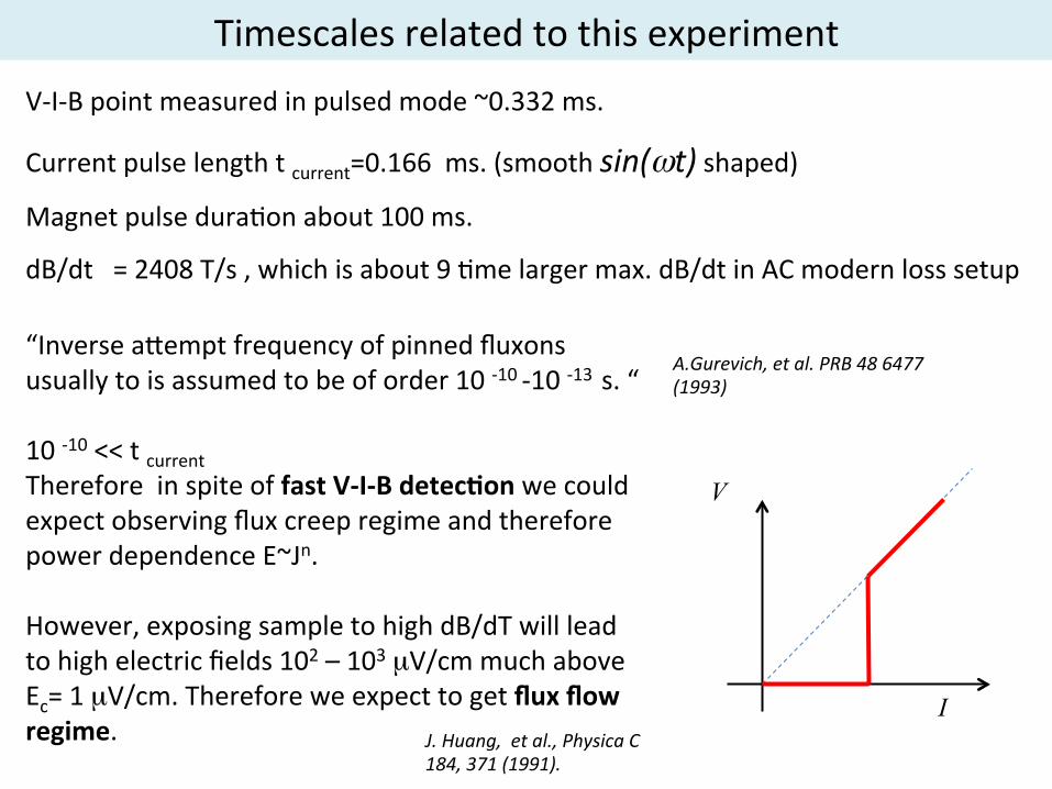
Timescales related to this experiment V-‐I-‐B point measured in pulsed mode ~0.332 ms.
Current pulse length t current=0.166 ms. (smooth sin(ωt) shaped) Magnet pulse dura*on about 100 ms.
dB/dt = 2408 T/s , which is about 9 *me larger max. dB/dt in AC modern loss setup
“Inverse aoempt frequency of pinned fluxons usually to is assumed to be of order 10 -‐10 -‐10 -‐13 s. “ 10 -‐10 << t current Therefore in spite of fast V-‐I-‐B detecXon we could expect observing flux creep regime and therefore power dependence E~Jn. However, exposing sample to high dB/dT will lead to high electric fields 102 – 103 µV/cm much above Ec= 1 µV/cm. Therefore we expect to get flux flow regime.
A.Gurevich, et al. PRB 48 6477 (1993)
J. Huang, et al., Physica C 184, 371 (1991).
I
V

Fixng Ic data from V(I,B) curves
To calculate Ic in experiments with DC field we use several I-‐V points near region of resis*ve transi*on by fixng data points with dependence 𝑉= 𝑉↓𝑐 (𝐼/𝐼↓𝑐 )↑𝑛 . During pulsed measurements we measure V(I, B) dependence, therefore fixng is more difficult:
For short periods of *me: 𝐵(𝑡)≈𝐵↓𝑜 + 𝑑𝐵/𝑑𝑡 𝑡 𝐼(𝑡)= 𝐼↓𝑜 + 𝑑𝐼/𝑑𝑡 𝑡
𝑉(𝐼,𝐵)= 𝑉↓𝑐 (𝐼/𝐼↓𝑐 (𝐵) )↑𝑛
𝐼↓𝑐 (𝐵)= 𝐼↓𝑐0 𝐵↑−𝛼
𝑉(𝐼)= 𝑉↓𝑐 (𝐼/𝐼↓𝑐0 (𝐵↓0 + 𝑑𝐵/𝑑𝐼 (𝐼− 𝐼↓0 ))↑−𝛼 )↑𝑛
𝐵(𝐼)≈𝐵↓0 + 𝑑𝐵/𝑑𝐼 (𝐼− 𝐼↓0 )
Combining above equa*ons together:
Within small field range
Too many fixng parameters
Near pulse peak we may add 𝑑↑2 𝐵/𝑑𝐼↑2 term
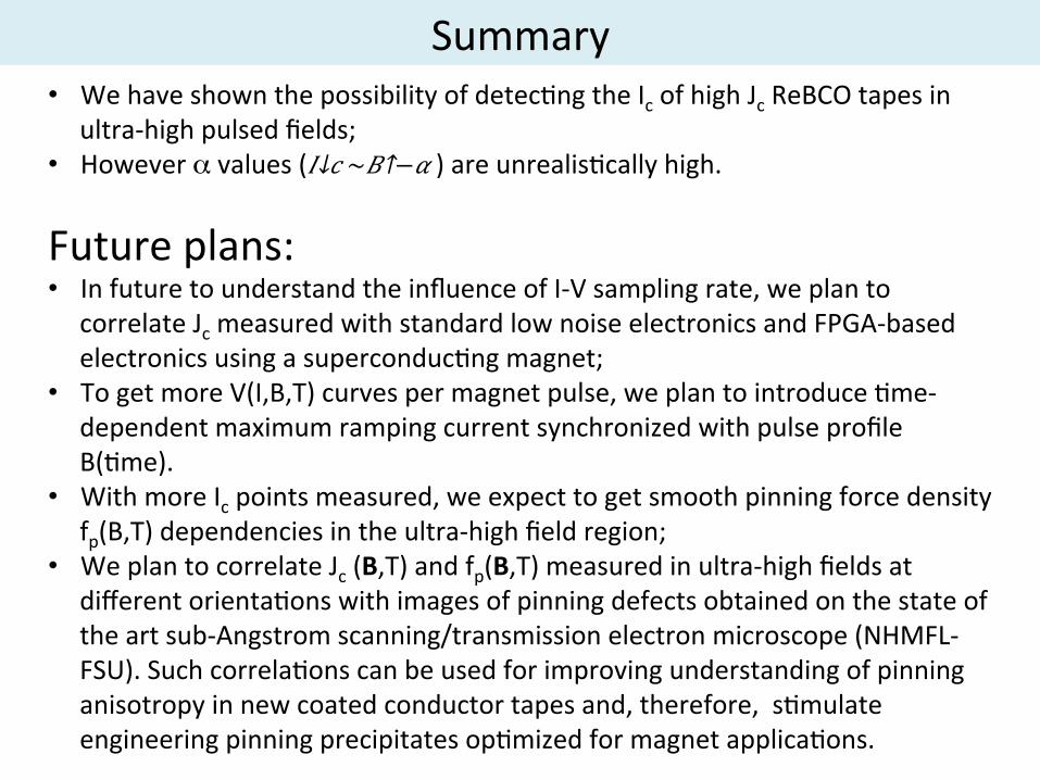
• We have shown the possibility of detec*ng the Ic of high Jc ReBCO tapes in ultra-‐high pulsed fields;
• However α values ( 𝐼↓𝑐 ~ 𝐵↑−𝛼 ) are unrealis*cally high.
Future plans: • In future to understand the influence of I-‐V sampling rate, we plan to
correlate Jc measured with standard low noise electronics and FPGA-‐based electronics using a superconduc*ng magnet;
• To get more V(I,B,T) curves per magnet pulse, we plan to introduce *me-‐dependent maximum ramping current synchronized with pulse profile B(*me).
• With more Ic points measured, we expect to get smooth pinning force density fp(B,T) dependencies in the ultra-‐high field region;
• We plan to correlate Jc (B,T) and fp(B,T) measured in ultra-‐high fields at different orienta*ons with images of pinning defects obtained on the state of the art sub-‐Angstrom scanning/transmission electron microscope (NHMFL-‐FSU). Such correla*ons can be used for improving understanding of pinning anisotropy in new coated conductor tapes and, therefore, s*mulate engineering pinning precipitates op*mized for magnet applica*ons.
Summary