characteristics of cmos
TRANSCRIPT
1 | P a g e
Characteristics of CMOS
CHARACTERISTICS OF CMOS
A Seminar Report
Submitted in Partial Fulfillment of the Requirements
for the Degree of
Bachelor of TECHNOLOGY
IN
ELECTRONICS & COMMUNICATION ENGINEERING
By Gunjan Gupta (10BEC112)
Jay Baxi (10BEC115)
Under the Guidance of Prof. Vijay Savani
Department of Electrical Engineering Electronics & Communication Engineering Program
Institute of Technology, Nirma University Ahmedabad-382481
November 2012
2 | P a g e
Characteristics of CMOS
CERTIFICATE
This is to certify that the Major Project Report entitled “FABRICATION AND
CHARACTERISTICS OF CMOS” submitted by Gunjan Gupta and Jay Baxi as the
partial fulfillment of the requirements for the award of the degree of Bachelor of
Technology in Electronics & Communication Engineering, Institute of Technology, Nirma
University is the record of work carried out by his under my supervision and guidance. The
work submitted in our opinion has reached a level required for being accepted for the
examination.
Date: November 08th, 2012
Prof. Vijay Savani
Project Guide
Dr. P. N. Tekwani
HOD (Electrical Engineering)
Nirma University, Ahmedabad
3 | P a g e
Characteristics of CMOS
Acknowledgement
We, Jay Baxi and Gunjan Gupta Students of Semester V, Institute of Technology, Nirma University have
presented a seminar on the topic CHARACTERISTICS OF CMOS under the guidance of Prof. Vijay
Savani.
We would like to sincerely thank Prof. Vijay Savani for his extreme support in making this seminar a
blissful journey. It would be impossible without his extreme surveillance and his kind guidance throughout
this journey of this seminar.
We would also like to thank HOD, Electrical Dept. Dr. P. N. Tekwani, for his support in making this
seminar possible.
4 | P a g e
Characteristics of CMOS
ABSTRACT
The electronics industry has achieved a phenomenal growth over the last few decades, mainly due to the
rapid advances in integration technologies and large-scale systems design. The use of integrated circuits in
high-performance computing, telecommunications, and consumer electronics has been growing at a very
fast pace. Typically, the required computational and information processing power of these applications is
the driving force for the fast development of this field.
The current leading edge technologies (such as low bit-rate video and cellular communications) already
give the provision to the end-users a certain amount of processing power and portability. This trend is
expected to continue, with very important implications for VLSI and systems design. One of the most
important characteristics of information services is their increasing need for very high processing power
and bandwidth (in order to handle real-time video, for example).
As more and more complex functions are required in various data processing and telecommunications
devices, the need to integrate these functions in a small package is also increasing. The level of integration
as measured by the number of logic gates in a monolithic chip has been steadily rising for almost three
decades, mainly due to the rapid progress in processing technology and interconnects technology.
All changed with the invention of the transistor at Bell Telephone Laboratories in, followed by the
introduction of the bipolar transistor by Schockley. The first truly successful IC logic family, TTL
(Transistor-Transistor Logic) was pioneered in 1962 [Beeson62]. Other logic families were devised with
higher performance in mind. Examples of these are the current switching circuits that produced the first
subnanosecond digital gates and culminated in the ECL (Emitter-Coupled Logic) family. TTL had the
advantage, however, of offering a higher integration density and was the basis of the first integrated circuit
revolution. In fact, the manufacturing of TTL components is what spear-headed the first large
semiconductor companies such as Fairchild, National, and Texas Instruments. The family was so
successful that it composed the largest fraction of the digital semiconductor market until the 1980s.
The basic principle behind the MOSFET transistor (originally called IGFET) was proposed in a patent by J.
Lilienfeld (Canada) as early as 1925, and, independently, by O. Heil in England in 1934. Insufficient
knowledge of the materials and gate stability problems, however, delayed the practical usability of the
device for a long time. Once these were solved, MOS digital integrated circuits started to take off in full in
the early 1970s. Remarkably, the first MOS logic gates introduced was of the CMOS variety, and this trend
continued till the late 1960s. The complexity of the manufacturing process delayed the full exploitation of
these devices for two more decades. Instead the first practical MOS integrated circuits were implemented
in PMOS-only logic and were used in applications such as calculators. The second age of the digital
integrated circuit revolution was inaugurated with the introduction of the first microprocessors by Intel in
1972 (the 4004) and 1974 (the 8080). These processors were implemented in NMOS-only logic, which has
the advantage of higher speed over the PMOS logic. Simultaneously, MOS technology enabled the
realization of the first high density semiconductor memories.
5 | P a g e
Characteristics of CMOS
Index
Chapter
No.
Title Page
No.
Certificate i
Acknowledgement Ii
Abstract iii
Index iv
List of Figures v
List of Tables vi
Nomenclature viii
1 MOS Transistor 9
2 MOS Transistor Under Static Condition 11
2.1 The Threshold Voltage
2.2 Resistive Operation
3 The MOSFET and calculation of Capacitance 15
3.1 The MOSFET Capacitances
3.2 Saturation Region
3.3 Channel Length Modulation
4 Drain Current versus Voltage charts 21
4.1 Sub-threshold Condition
5 The Voltage-Transfer Characteristic 25
6 Energy Band Diagram 28
7 nMOS External Biasing 31
8 pMOS Modes of Operation 34
9 Summary 36
References 37
6 | P a g e
Characteristics of CMOS
LIST OF FIGURES
Fig. No.
Title Page No.
1.1 Cross Section featuring n-well CMOS process. 9
1.2 Single Crystalline lightly doped wafer 9
2.1 Relationship between Vt vs Vbs 12
2.2 p-substrate Resistive Operation 13
3.1 Symbols used for n- and p-channel MOSFETs. 15
3.2 Cross-sectional view of MOSFET used to calculate capacitances 16
3.3 MOSFET in accumulation 17
3.4 MOSFET in depletion 17
3.5 Capacitance to ground at gate terminal of the circuit vs gate-source voltage. 18
3.6 MOSFET capacitances 19
3.7 Saturation Region 19
4.1 Long-channel transistor and Short-channel Transistor 20
4.2 Long-channel device and Short-channel device 21
4.3 Relation between Id vs Vds 22
4.4 ID current versus VGS (on logarithmic scale) 23
5.1 Voltage transfer characteristic of an inverter. 25
5.2 Different output of the gate connected to an input signal. 25
5.3 Gate Output to next stage with Noise Margins 26
5.4 Cascaded inverter gates: Definition of Noise Margins 26
5.5 Regenerative Property 27
6.1 Energy Band Diagram for nMOS 28
6.2 EBD for different kind of materials for nMOS 29
6.3 Resulting Band Diagram Of The Mos System 30
7.1 Accumulation Region for nMOS 31
7.2 Saturation Region for nMOS 31
7.3 Inversion Region for nMOS 33
8 pMOS modes of operation 34
7 | P a g e
Characteristics of CMOS
TABLE
3.1 MOSFET capacitances 18
8 | P a g e
Characteristics of CMOS
NOMENCLATURE
A Energy level indicator
B Bottom product rate, kmol/hr
Greek
Θ Root of Underwood equation
Α Relative volatility
Λ Latent heat of vaporization, kcal/kmol
Difference
Ε Energy change indicator
Subscripts
Min Minimum
I Any component
Abbreviations
EBD Energy Band Diagram
9 | P a g e
Characteristics of CMOS
1. MOS Transistor
Most digital designers will never be confronted with the details of the manufacturing process that lies at the
core of the semiconductor revolution. Yet, some insight in the steps that lead to an operational silicon chip
comes in quite handy in understanding the physical constraints that are imposed on a designer of an
integrated circuit, as well as the impact of the fabrication process on issues such as cost.
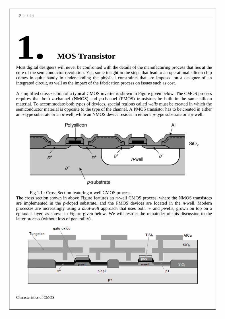
A simplified cross section of a typical CMOS inverter is shown in Figure given below. The CMOS process
requires that both n-channel (NMOS) and p-channel (PMOS) transistors be built in the same silicon
material. To accommodate both types of devices, special regions called wells must be created in which the
semiconductor material is opposite to the type of the channel. A PMOS transistor has to be created in either
an n-type substrate or an n-well, while an NMOS device resides in either a p-type substrate or a p-well.
Fig 1.1 : Cross Section featuring n-well CMOS process.
The cross section shown in above Figure features an n-well CMOS process, where the NMOS transistors
are implemented in the p-doped substrate, and the PMOS devices are located in the n-well. Modern
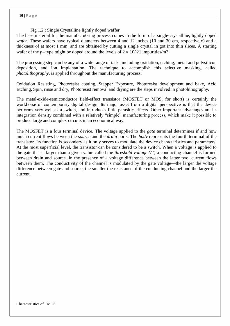
processes are increasingly using a dual-well approach that uses both n- and pwells, grown on top on a
epitaxial layer, as shown in Figure given below. We will restrict the remainder of this discussion to the
latter process (without loss of generality).
10 | P a g e
Characteristics of CMOS
Fig 1.2 : Single Crystalline lightly doped waffer
The base material for the manufactu0ring process comes in the form of a single-crystalline, lightly doped
wafer. These wafers have typical diameters between 4 and 12 inches (10 and 30 cm, respectively) and a
thickness of at most 1 mm, and are obtained by cutting a single crystal in got into thin slices. A starting
wafer of the p--type might be doped around the levels of 2 10^21 impurities/m3.
The processing step can be any of a wide range of tasks including oxidation, etching, metal and polysilicon
deposition, and ion implantation. The technique to accomplish this selective masking, called
photolithography, is applied throughout the manufacturing process.
Oxidation Resisting, Photoresist coating, Stepper Exposure, Photoresist development and bake, Acid
Etching, Spin, rinse and dry, Photoresist removal and drying are the steps involved in photolithography.
The metal-oxide-semiconductor field-effect transistor (MOSFET or MOS, for short) is certainly the
workhorse of contemporary digital design. Its major asset from a digital perspective is that the device
performs very well as a switch, and introduces little parasitic effects. Other important advantages are its
integration density combined with a relatively “simple” manufacturing process, which make it possible to
produce large and complex circuits in an economical way.
The MOSFET is a four terminal device. The voltage applied to the gate terminal determines if and how
much current flows between the source and the drain ports. The body represents the fourth terminal of the
transistor. Its function is secondary as it only serves to modulate the device characteristics and parameters.
At the most superficial level, the transistor can be considered to be a switch. When a voltage is applied to
the gate that is larger than a given value called the threshold voltage VT, a conducting channel is formed
between drain and source. In the presence of a voltage difference between the latter two, current flows
between them. The conductivity of the channel is modulated by the gate voltage—the larger the voltage
difference between gate and source, the smaller the resistance of the conducting channel and the larger the
current.
11 | P a g e
Characteristics of CMOS
2. MOS TRANSISTOR UNDER STATIC CONDITIONS
In the derivation of the static model of the MOS transistor, we concentrate on the NMOS device. All the
arguments made are valid for PMOS devices as well as will be discussed at the end of the section.
2.1 The Threshold Voltage Consider first the case where VGS = 0 and drain, source, and bulk are connected to ground. The drain and
source are connected by back-to-back pn-junctions (substrate-source and substrate-drain). Under the
mentioned conditions, both junctions have a 0 V bias and can be considered off, which results in an
extremely high resistance between drain and source. Assume now that a positive voltage is applied to the
gate (with respect to the source). The gate and substrate form the plates of a capacitor with the gate oxide
as the dielectric. The positive gate voltage causes positive charge to accumulate on the gate electrode and
negative charge on the substrate side. The latter manifests it initially by repelling mobile holes. Hence, a
depletion region is formed below the gate. This depletion region is similar to the one occurring in a pn-
junction diode. Consequently, similar expressions hold for the width and the space charge per unit area
(2.1)
(2.2)
with NA the substrate doping and the voltage across the depletion layer (i.e., the potential at the oxide-
silicon boundary).
As the gate voltage increases, the potential at the silicon surface at some point reaches a critical value,
where the semiconductor surface inverts to n-type material. This point marks the onset of a phenomenon
known as strong inversion and occurs at a voltage
equal to twice the Fermi Potential) (F 0.3 V for typical p-type silicon substrates):
(2.3)
Further increases in the gate voltage produce no further changes in the depletion layer width, but result in
additional electrons in the thin inversion layer directly under the oxide. These are drawn into the inversion
layer from the heavily doped n+ source region. Hence, a continuous n-type channel is formed between the
source and drain regions, the conductivity of which is modulated by the gate-source voltage.
This picture changes somewhat in case a substrate bias voltage VSB is applied (VSB is normally positive
for n-channel devices). This causes the surface potential required for strong inversion to increase and to
become |–2F + VSB|. The charge stored in the depletion region now is expressed by Eq 3.1.
12 | P a g e
Characteristics of CMOS
(2.4)
(2.5)
The value of VGS where strong inversion occurs is called the threshold voltage VT. VT is a function of
several components, most of which are material constants such as the difference in work-function between
gate and substrate material, the oxide thickness, the Fermi voltage, the charge of impurities trapped at the
surface between channel and gate oxide, and the dosage of ions implanted for threshold adjustment. From
the above arguments, it has become clear that the source-bulk voltage VSB has an impact on the threshold
as well. Rather than relying on a complex (and hardly accurate) analytical expression for the threshold, we
rely on an empirical parameter called VT, which is the threshold voltage for VSB = , and is mostly a
function of the manufacturing process. The threshold voltage under different body-biasing conditions can
then be determined in the following manner,
(2.6)
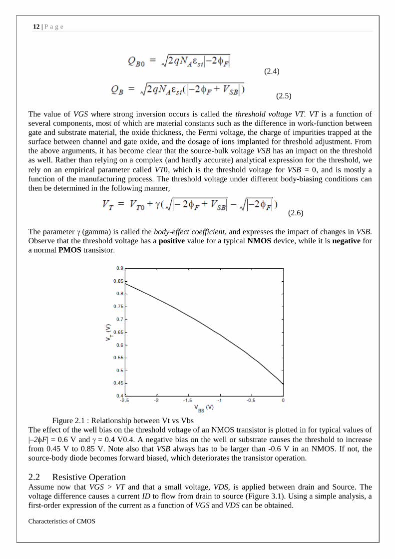
The parameter (gamma) is called the body-effect coefficient, and expresses the impact of changes in VSB.
Observe that the threshold voltage has a positive value for a typical NMOS device, while it is negative for
a normal PMOS transistor.
Figure 2.1 : Relationship between Vt vs Vbs
The effect of the well bias on the threshold voltage of an NMOS transistor is plotted in for typical values of
|–2F| = 0.6 V and = 0.4 V0.4. A negative bias on the well or substrate causes the threshold to increase
from 0.45 V to 0.85 V. Note also that VSB always has to be larger than -0.6 V in an NMOS. If not, the
source-body diode becomes forward biased, which deteriorates the transistor operation.
2.2 Resistive Operation Assume now that VGS > VT and that a small voltage, VDS, is applied between drain and Source. The
voltage difference causes a current ID to flow from drain to source (Figure 3.1). Using a simple analysis, a
first-order expression of the current as a function of VGS and VDS can be obtained.
13 | P a g e
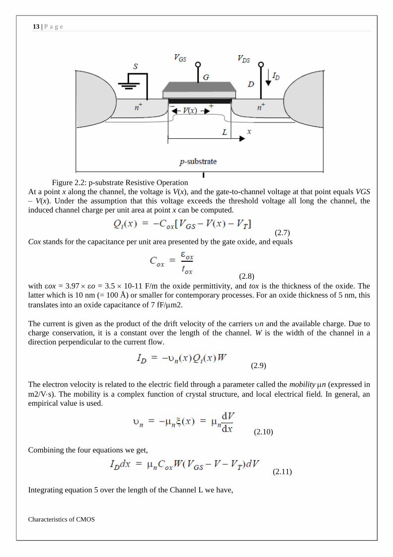
Characteristics of CMOS
Figure 2.2: p-substrate Resistive Operation
At a point x along the channel, the voltage is V(x), and the gate-to-channel voltage at that point equals VGS
– V(x). Under the assumption that this voltage exceeds the threshold voltage all long the channel, the
induced channel charge per unit area at point x can be computed.
(2.7)
Cox stands for the capacitance per unit area presented by the gate oxide, and equals
(2.8)
with ox = 3.97o = 3.5 10-11 F/m the oxide permittivity, and tox is the thickness of the oxide. The
latter which is 10 nm (= 100 Å) or smaller for contemporary processes. For an oxide thickness of 5 nm, this
translates into an oxide capacitance of 7 fF/m2.
The current is given as the product of the drift velocity of the carriers n and the available charge. Due to
charge conservation, it is a constant over the length of the channel. W is the width of the channel in a
direction perpendicular to the current flow.
(2.9)
The electron velocity is related to the electric field through a parameter called the mobility n (expressed in
m2/Vs). The mobility is a complex function of crystal structure, and local electrical field. In general, an
empirical value is used.
(2.10)
Combining the four equations we get,
(2.11)
Integrating equation 5 over the length of the Channel L we have,
14 | P a g e
Characteristics of CMOS
(2.12)
This yields the voltage-current relation of the transistor.
K’n is called the transconductance parameter and is given by the following expression,
(2.13)
The product of the process transconductance and the (W/L) ratio of an (NMOS) transistor is called the gain
factor kn of the device. For smaller values of VDS, the quadratic factor in Eq. can be ignored, and we
observe a linear dependence between VDS and ID. The operation region where Eq. holds is hence called
the resistive or linear region. One of its main properties is that it displays a continuous conductive channel
between source and drain regions.
The W and L parameters in Eq. represent the effective channel width and length of the transistor. These
values differ from the dimensions drawn on the layout due to effects such as lateral diffusion of the source
and drain regions (L), and the encroachment of the isolating field oxide (W). In the remainder of the text, W
and L will always stand for the effective dimensions, while a d subscript will be used to indicate the drawn
size. The following expressions related the two parameters, with W and L parameters of the
manufacturing process:
W = Wd – W
L = Ld – L
15 | P a g e
Characteristics of CMOS
3. The MOSFET and calculation of Capacitance
At this point we should have some appreciation for the parasitics, that is, capacitances and resistances,
associated with a CMOS process. In this chapter we discuss the MOSFET operation. To begin let's define
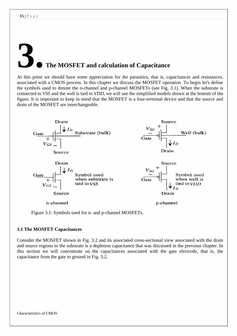
the symbols used to denote the n-channel and p-channel MOSFETs (see Fig. 3.1). When the substrate is
connected to VSS and the well is tied to VDD, we will use the simplified models shown at the bottom of the
figure. It is important to keep in mind that the MOSFET is a four-terminal device and that the source and
drain of the MOSFET are interchangeable.
Figure 3.1: Symbols used for n- and p-channel MOSFETs.
3.1 The MOSFET Capacitances
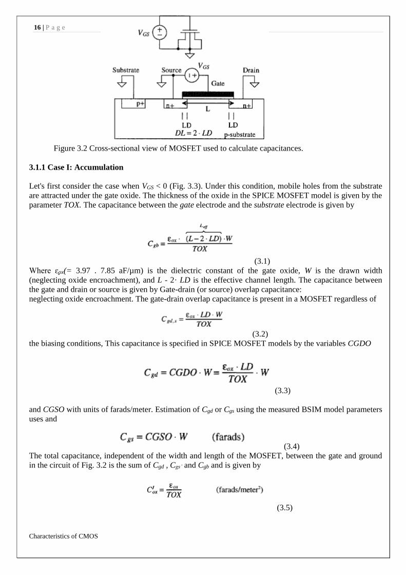
Consider the MOSFET shown in Fig. 3.2 and its associated cross-sectional view associated with the drain
and source regions to the substrate is a depletion capacitance that was discussed in the previous chapter. In
this section we will concentrate on the capacitances associated with the gate electrode, that is, the
capacitance from the gate to ground in Fig. 3.2.
16 | P a g e
Characteristics of CMOS
Figure 3.2 Cross-sectional view of MOSFET used to calculate capacitances.
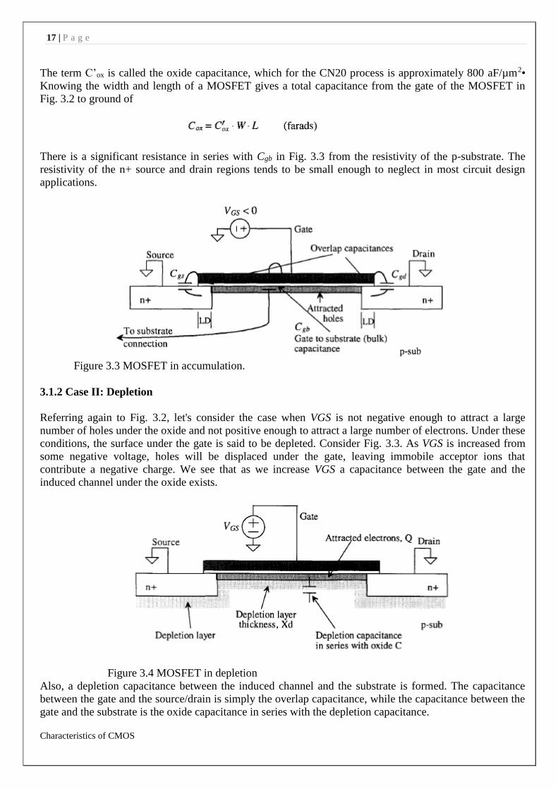
3.1.1 Case I: Accumulation
Let's first consider the case when VGS < 0 (Fig. 3.3). Under this condition, mobile holes from the substrate
are attracted under the gate oxide. The thickness of the oxide in the SPICE MOSFET model is given by the
parameter TOX. The capacitance between the gate electrode and the substrate electrode is given by
(3.1)
Where ᶓox(= 3.97 . 7.85 aF/µm) is the dielectric constant of the gate oxide, W is the drawn width
(neglecting oxide encroachment), and L - 2· LD is the effective channel length. The capacitance between
the gate and drain or source is given by Gate-drain (or source) overlap capacitance:
neglecting oxide encroachment. The gate-drain overlap capacitance is present in a MOSFET regardless of
(3.2)
the biasing conditions, This capacitance is specified in SPICE MOSFET models by the variables CGDO
(3.3)
and CGSO with units of farads/meter. Estimation of Cgd or Cgs using the measured BSIM model parameters
uses and
(3.4)
The total capacitance, independent of the width and length of the MOSFET, between the gate and ground
in the circuit of Fig. 3.2 is the sum of Cgd , Cgs’ and Cgb and is given by
(3.5)
17 | P a g e
Characteristics of CMOS
The term C’ox is called the oxide capacitance, which for the CN20 process is approximately 800 aF/µm2•
Knowing the width and length of a MOSFET gives a total capacitance from the gate of the MOSFET in
Fig. 3.2 to ground of
There is a significant resistance in series with Cgb in Fig. 3.3 from the resistivity of the p-substrate. The
resistivity of the n+ source and drain regions tends to be small enough to neglect in most circuit design
applications.
Figure 3.3 MOSFET in accumulation.
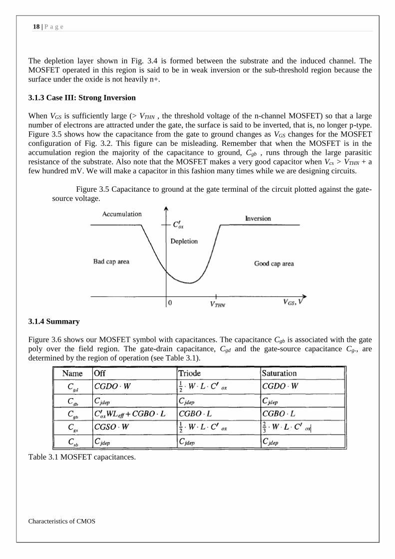
3.1.2 Case II: Depletion
Referring again to Fig. 3.2, let's consider the case when VGS is not negative enough to attract a large
number of holes under the oxide and not positive enough to attract a large number of electrons. Under these
conditions, the surface under the gate is said to be depleted. Consider Fig. 3.3. As VGS is increased from
some negative voltage, holes will be displaced under the gate, leaving immobile acceptor ions that
contribute a negative charge. We see that as we increase VGS a capacitance between the gate and the
induced channel under the oxide exists.
Figure 3.4 MOSFET in depletion
Also, a depletion capacitance between the induced channel and the substrate is formed. The capacitance
between the gate and the source/drain is simply the overlap capacitance, while the capacitance between the
gate and the substrate is the oxide capacitance in series with the depletion capacitance.
18 | P a g e
Characteristics of CMOS
The depletion layer shown in Fig. 3.4 is formed between the substrate and the induced channel. The
MOSFET operated in this region is said to be in weak inversion or the sub-threshold region because the
surface under the oxide is not heavily n+.
3.1.3 Case III: Strong Inversion
When VGS is sufficiently large (> VTHN , the threshold voltage of the n-channel MOSFET) so that a large
number of electrons are attracted under the gate, the surface is said to be inverted, that is, no longer p-type.
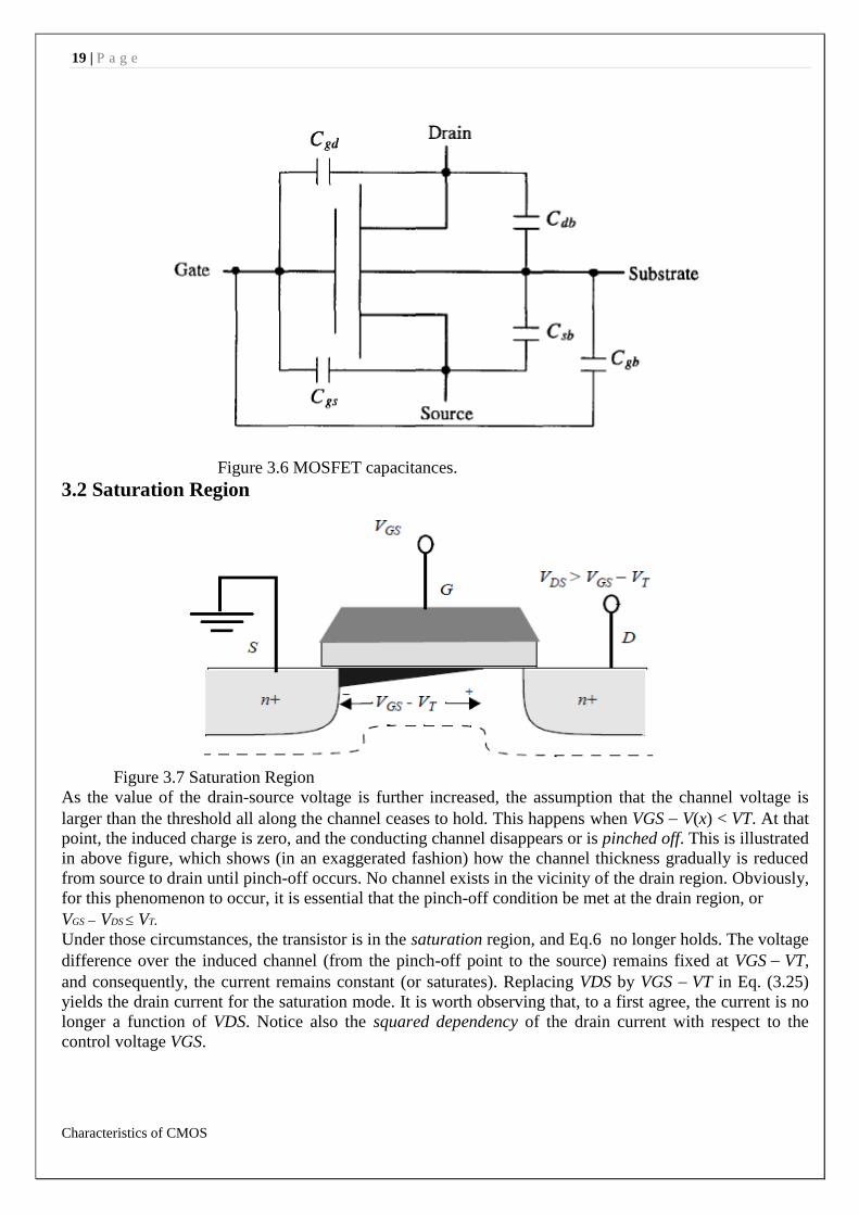
Figure 3.5 shows how the capacitance from the gate to ground changes as VGS changes for the MOSFET
configuration of Fig. 3.2. This figure can be misleading. Remember that when the MOSFET is in the
accumulation region the majority of the capacitance to ground, Cgb , runs through the large parasitic
resistance of the substrate. Also note that the MOSFET makes a very good capacitor when Vcs > VTHN + a
few hundred mV. We will make a capacitor in this fashion many times while we are designing circuits.
Figure 3.5 Capacitance to ground at the gate terminal of the circuit plotted against the gate-
source voltage.
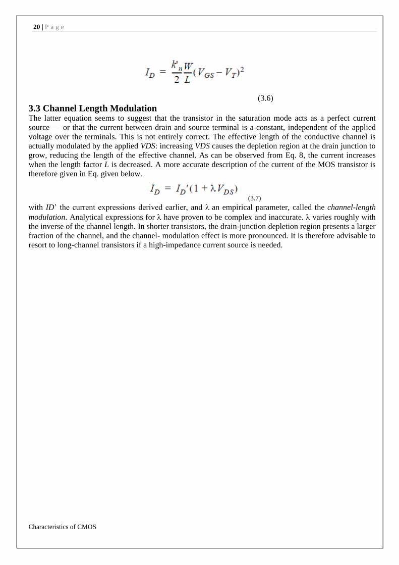
3.1.4 Summary
Figure 3.6 shows our MOSFET symbol with capacitances. The capacitance Cgb is associated with the gate
poly over the field region. The gate-drain capacitance, Cgd and the gate-source capacitance Cg., are
determined by the region of operation (see Table 3.1).
Table 3.1 MOSFET capacitances.
19 | P a g e
Characteristics of CMOS
Figure 3.6 MOSFET capacitances.
3.2 Saturation Region
Figure 3.7 Saturation Region
As the value of the drain-source voltage is further increased, the assumption that the channel voltage is
larger than the threshold all along the channel ceases to hold. This happens when VGS V(x) < VT. At that
point, the induced charge is zero, and the conducting channel disappears or is pinched off. This is illustrated
in above figure, which shows (in an exaggerated fashion) how the channel thickness gradually is reduced
from source to drain until pinch-off occurs. No channel exists in the vicinity of the drain region. Obviously,
for this phenomenon to occur, it is essential that the pinch-off condition be met at the drain region, or
VGSVDS VT.
Under those circumstances, the transistor is in the saturation region, and Eq.6 no longer holds. The voltage
difference over the induced channel (from the pinch-off point to the source) remains fixed at VGSVT,
and consequently, the current remains constant (or saturates). Replacing VDS by VGS VT in Eq. (3.25)
yields the drain current for the saturation mode. It is worth observing that, to a first agree, the current is no
longer a function of VDS. Notice also the squared dependency of the drain current with respect to the
control voltage VGS.
20 | P a g e
Characteristics of CMOS
(3.6)
3.3 Channel Length Modulation The latter equation seems to suggest that the transistor in the saturation mode acts as a perfect current
source — or that the current between drain and source terminal is a constant, independent of the applied
voltage over the terminals. This is not entirely correct. The effective length of the conductive channel is
actually modulated by the applied VDS: increasing VDS causes the depletion region at the drain junction to
grow, reducing the length of the effective channel. As can be observed from Eq. 8, the current increases
when the length factor L is decreased. A more accurate description of the current of the MOS transistor is
therefore given in Eq. given below.
(3.7)
with ID’ the current expressions derived earlier, and an empirical parameter, called the channel-length
modulation. Analytical expressions for have proven to be complex and inaccurate. varies roughly with
the inverse of the channel length. In shorter transistors, the drain-junction depletion region presents a larger
fraction of the channel, and the channel- modulation effect is more pronounced. It is therefore advisable to
resort to long-channel transistors if a high-impedance current source is needed.
21 | P a g e
Characteristics of CMOS
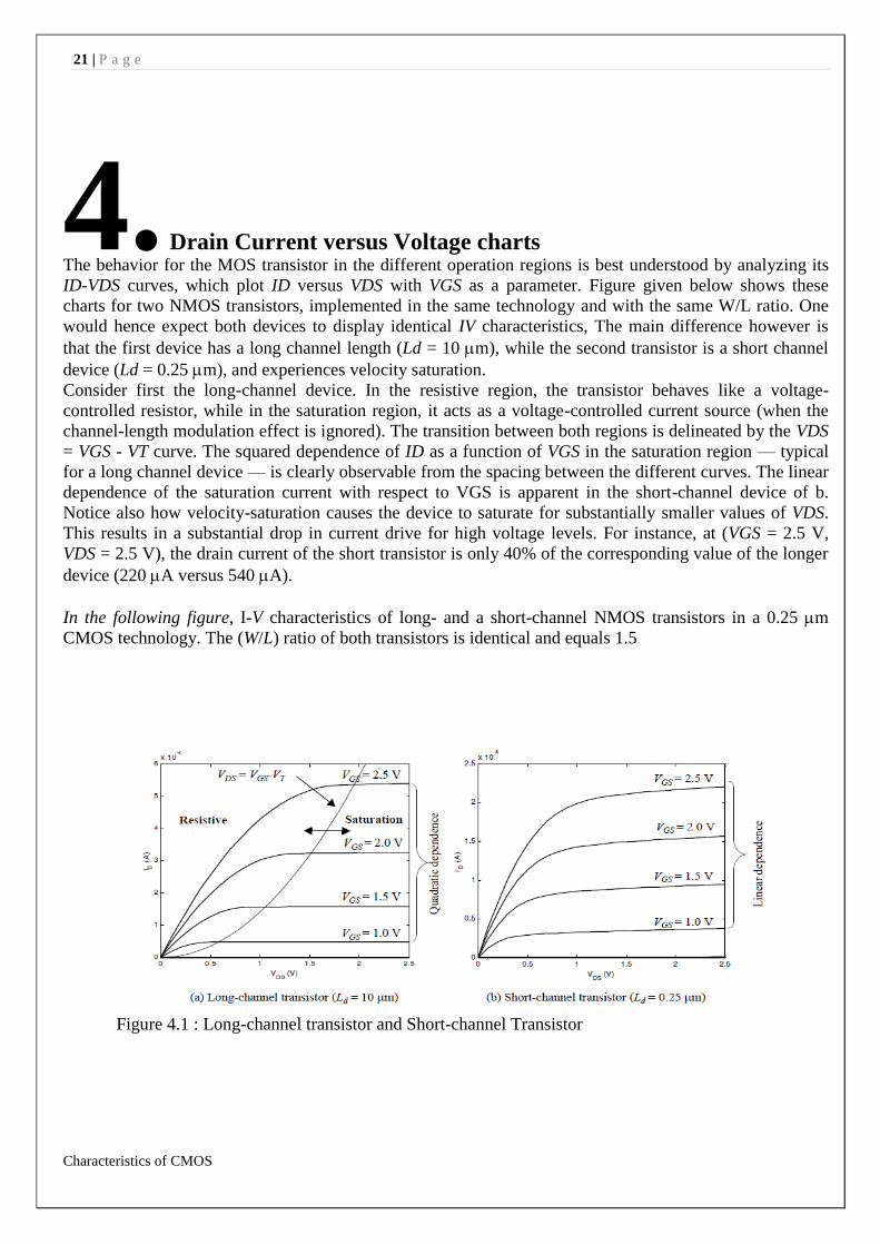
4. Drain Current versus Voltage charts The behavior for the MOS transistor in the different operation regions is best understood by analyzing its
ID-VDS curves, which plot ID versus VDS with VGS as a parameter. Figure given below shows these
charts for two NMOS transistors, implemented in the same technology and with the same W/L ratio. One
would hence expect both devices to display identical IV characteristics, The main difference however is
that the first device has a long channel length (Ld = 10 m), while the second transistor is a short channel
device (Ld = 0.25 m), and experiences velocity saturation.
Consider first the long-channel device. In the resistive region, the transistor behaves like a voltage-
controlled resistor, while in the saturation region, it acts as a voltage-controlled current source (when the
channel-length modulation effect is ignored). The transition between both regions is delineated by the VDS
= VGS - VT curve. The squared dependence of ID as a function of VGS in the saturation region — typical
for a long channel device — is clearly observable from the spacing between the different curves. The linear
dependence of the saturation current with respect to VGS is apparent in the short-channel device of b.
Notice also how velocity-saturation causes the device to saturate for substantially smaller values of VDS.
This results in a substantial drop in current drive for high voltage levels. For instance, at (VGS = 2.5 V,
VDS = 2.5 V), the drain current of the short transistor is only 40% of the corresponding value of the longer
device (220 A versus 540 A).
In the following figure, I-V characteristics of long- and a short-channel NMOS transistors in a 0.25 m
CMOS technology. The (W/L) ratio of both transistors is identical and equals 1.5
Figure 4.1 : Long-channel transistor and Short-channel Transistor
22 | P a g e
Characteristics of CMOS
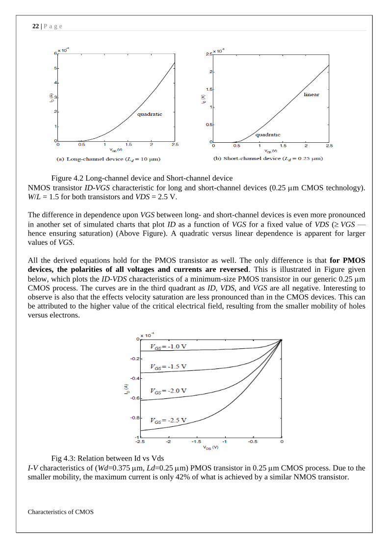
Figure 4.2 Long-channel device and Short-channel device
NMOS transistor ID-VGS characteristic for long and short-channel devices (0.25 m CMOS technology).
W/L = 1.5 for both transistors and VDS = 2.5 V.
The difference in dependence upon VGS between long- and short-channel devices is even more pronounced
in another set of simulated charts that plot ID as a function of VGS for a fixed value of VDS (VGS —
hence ensuring saturation) (Above Figure). A quadratic versus linear dependence is apparent for larger
values of VGS.
All the derived equations hold for the PMOS transistor as well. The only difference is that for PMOS
devices, the polarities of all voltages and currents are reversed. This is illustrated in Figure given
below, which plots the ID-VDS characteristics of a minimum-size PMOS transistor in our generic 0.25 m
CMOS process. The curves are in the third quadrant as ID, VDS, and VGS are all negative. Interesting to
observe is also that the effects velocity saturation are less pronounced than in the CMOS devices. This can
be attributed to the higher value of the critical electrical field, resulting from the smaller mobility of holes
versus electrons.
Fig 4.3: Relation between Id vs Vds
I-V characteristics of (Wd=0.375 m, Ld=0.25 m) PMOS transistor in 0.25 m CMOS process. Due to the
smaller mobility, the maximum current is only 42% of what is achieved by a similar NMOS transistor.
23 | P a g e
Characteristics of CMOS
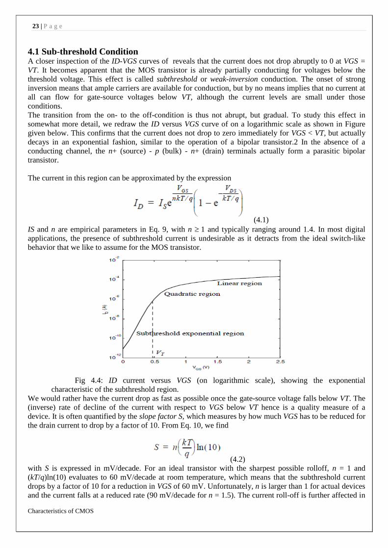
4.1 Sub-threshold Condition A closer inspection of the ID-VGS curves of reveals that the current does not drop abruptly to 0 at VGS =
VT. It becomes apparent that the MOS transistor is already partially conducting for voltages below the
threshold voltage. This effect is called subthreshold or weak-inversion conduction. The onset of strong
inversion means that ample carriers are available for conduction, but by no means implies that no current at
all can flow for gate-source voltages below VT, although the current levels are small under those
conditions.
The transition from the on- to the off-condition is thus not abrupt, but gradual. To study this effect in
somewhat more detail, we redraw the ID versus VGS curve of on a logarithmic scale as shown in Figure
given below. This confirms that the current does not drop to zero immediately for VGS < VT, but actually
decays in an exponential fashion, similar to the operation of a bipolar transistor.2 In the absence of a
conducting channel, the n+ (source) - p (bulk) - n+ (drain) terminals actually form a parasitic bipolar
transistor.
The current in this region can be approximated by the expression
(4.1)
IS and n are empirical parameters in Eq. 9, with n 1 and typically ranging around 1.4. In most digital
applications, the presence of subthreshold current is undesirable as it detracts from the ideal switch-like
behavior that we like to assume for the MOS transistor.
Fig 4.4: ID current versus VGS (on logarithmic scale), showing the exponential
characteristic of the subthreshold region.
We would rather have the current drop as fast as possible once the gate-source voltage falls below VT. The
(inverse) rate of decline of the current with respect to VGS below VT hence is a quality measure of a
device. It is often quantified by the slope factor S, which measures by how much VGS has to be reduced for
the drain current to drop by a factor of 10. From Eq. 10, we find
(4.2)
with S is expressed in mV/decade. For an ideal transistor with the sharpest possible rolloff, n = 1 and
(kT/q)ln(10) evaluates to 60 mV/decade at room temperature, which means that the subthreshold current
drops by a factor of 10 for a reduction in VGS of 60 mV. Unfortunately, n is larger than 1 for actual devices
and the current falls at a reduced rate (90 mV/decade for n = 1.5). The current roll-off is further affected in
24 | P a g e
Characteristics of CMOS
a negative sense by an increase in the operating temperature (most integrated circuits operate at
temperatures considerably beyond room temperature). The value of n is determined by the intrinsic device
topology and structure. Reducing its value hence requires a different process technology, such as silicon-
on-insulator.
Subthreshold current has some important repercussions. In general, we want the current through the
transistor to be as close as possible to zero at VGS = 0. This is especially important in the so-called
dynamic circuits, which rely on the storage of charge on a capacitor and whose operation can be severely
degraded by subthreshold leakage. Achieving this in the presence of subthreshold current requires a firm
lower bound on the value of the threshold voltage of the devices.
A word of caution — The model presented here is derived from the characteristics of a single device with
a minimum channel-length and width. Trying to extrapolate this behavior to devices with substantially
different values of W and L will probably lead to sizable errors. Fortunately, digital circuits typically use
only minimum-length devices as these lead to the smallest implementation area. Matching for these
transistors will typically be acceptable. It is however advisable to use a different set of model parameters
for devices with dramatically different size- and shape-factors.
25 | P a g e
Characteristics of CMOS
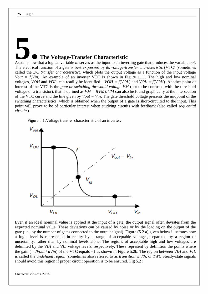
5. The Voltage-Transfer Characteristic Assume now that a logical variable in serves as the input to an inverting gate that produces the variable out.
The electrical function of a gate is best expressed by its voltage-transfer characteristic (VTC) (sometimes
called the DC transfer characteristic), which plots the output voltage as a function of the input voltage
Vout = f(Vin). An example of an inverter VTC is shown in Figure 1.11. The high and low nominal
voltages, VOH and VOL, can readily be identified—VOH = f(VOL) and VOL = f(VOH). Another point of
interest of the VTC is the gate or switching threshold voltage VM (not to be confused with the threshold
voltage of a transistor), that is defined as VM = f(VM). VM can also be found graphically at the intersection
of the VTC curve and the line given by Vout = Vin. The gate threshold voltage presents the midpoint of the
switching characteristics, which is obtained when the output of a gate is short-circuited to the input. This
point will prove to be of particular interest when studying circuits with feedback (also called sequential
circuits).
Figure 5.1:Voltage transfer characteristic of an inverter.
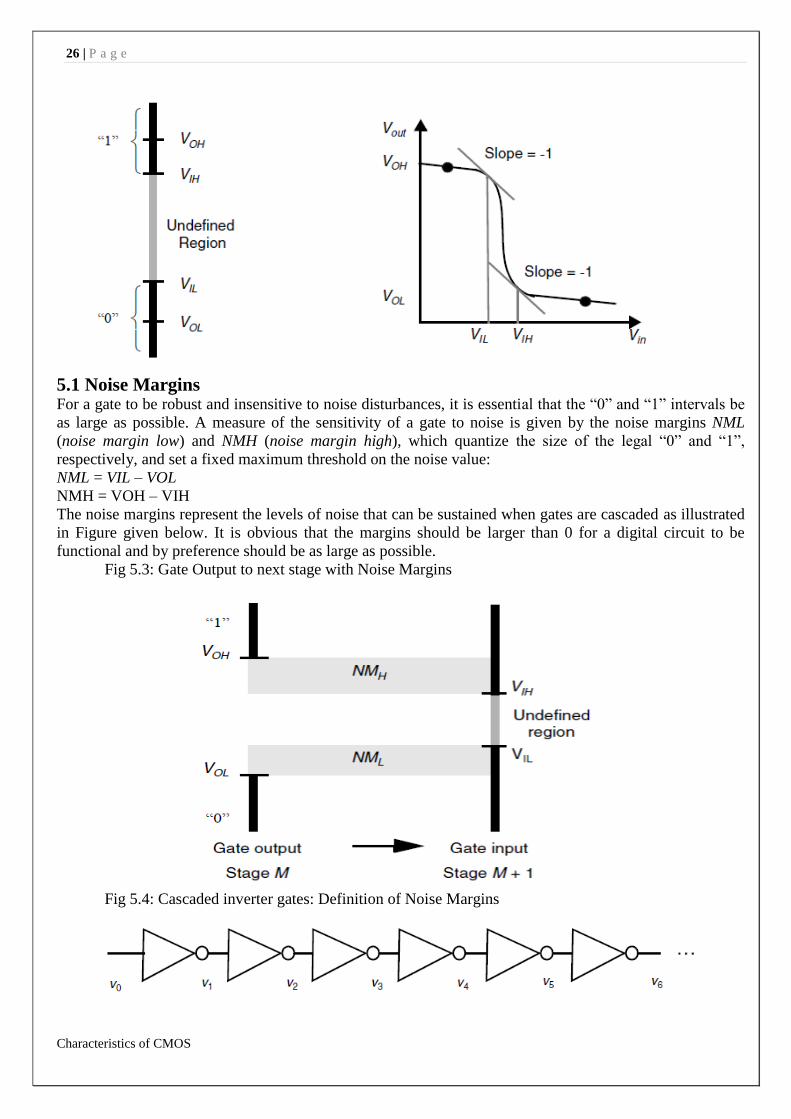
Even if an ideal nominal value is applied at the input of a gate, the output signal often deviates from the
expected nominal value. These deviations can be caused by noise or by the loading on the output of the
gate (i.e., by the number of gates connected to the output signal). Figure (5.2 a) given below illustrates how
a logic level is represented in reality by a range of acceptable voltages, separated by a region of
uncertainty, rather than by nominal levels alone. The regions of acceptable high and low voltages are
delimited by the VIH and VIL voltage levels, respectively. These represent by definition the points where
the gain (= dVout / dVin) of the VTC equals 1 as shown in Figure 5.2b. The region between VIH and VIL
is called the undefined region (sometimes also referred to as transition width, or TW). Steady-state signals
should avoid this region if proper circuit operation is to be ensured. Fig 5.2 :
26 | P a g e
Characteristics of CMOS
5.1 Noise Margins For a gate to be robust and insensitive to noise disturbances, it is essential that the “0” and “1” intervals be
as large as possible. A measure of the sensitivity of a gate to noise is given by the noise margins NML
(noise margin low) and NMH (noise margin high), which quantize the size of the legal “0” and “1”,
respectively, and set a fixed maximum threshold on the noise value:
NML = VIL – VOL
NMH = VOH – VIH
The noise margins represent the levels of noise that can be sustained when gates are cascaded as illustrated
in Figure given below. It is obvious that the margins should be larger than 0 for a digital circuit to be
functional and by preference should be as large as possible.
Fig 5.3: Gate Output to next stage with Noise Margins
Fig 5.4: Cascaded inverter gates: Definition of Noise Margins
27 | P a g e
Characteristics of CMOS
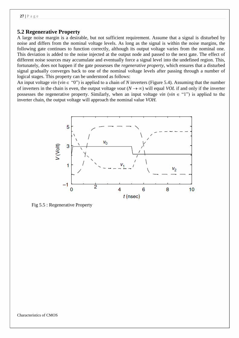
5.2 Regenerative Property A large noise margin is a desirable, but not sufficient requirement. Assume that a signal is disturbed by
noise and differs from the nominal voltage levels. As long as the signal is within the noise margins, the
following gate continues to function correctly, although its output voltage varies from the nominal one.
This deviation is added to the noise injected at the output node and passed to the next gate. The effect of
different noise sources may accumulate and eventually force a signal level into the undefined region. This,
fortunately, does not happen if the gate possesses the regenerative property, which ensures that a disturbed
signal gradually converges back to one of the nominal voltage levels after passing through a number of
logical stages. This property can be understood as follows:
An input voltage vin (vin “0”) is applied to a chain of N inverters (Figure 5.4). Assuming that the number
of inverters in the chain is even, the output voltage vout (N ) will equal VOL if and only if the inverter
possesses the regenerative property. Similarly, when an input voltage vin (vin “1”) is applied to the
inverter chain, the output voltage will approach the nominal value VOH.
Fig 5.5 : Regenerative Property
28 | P a g e
Characteristics of CMOS
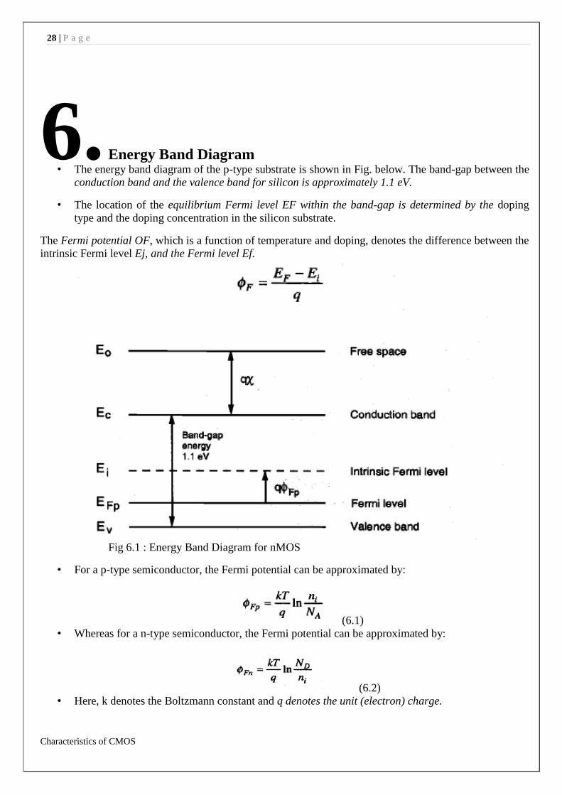
6. Energy Band Diagram • The energy band diagram of the p-type substrate is shown in Fig. below. The band-gap between the
conduction band and the valence band for silicon is approximately 1.1 eV.
• The location of the equilibrium Fermi level EF within the band-gap is determined by the doping
type and the doping concentration in the silicon substrate.
The Fermi potential OF, which is a function of temperature and doping, denotes the difference between the
intrinsic Fermi level Ej, and the Fermi level Ef.
Fig 6.1 : Energy Band Diagram for nMOS
• For a p-type semiconductor, the Fermi potential can be approximated by:
(6.1)
• Whereas for a n-type semiconductor, the Fermi potential can be approximated by:
(6.2)
• Here, k denotes the Boltzmann constant and q denotes the unit (electron) charge.
29 | P a g e
Characteristics of CMOS
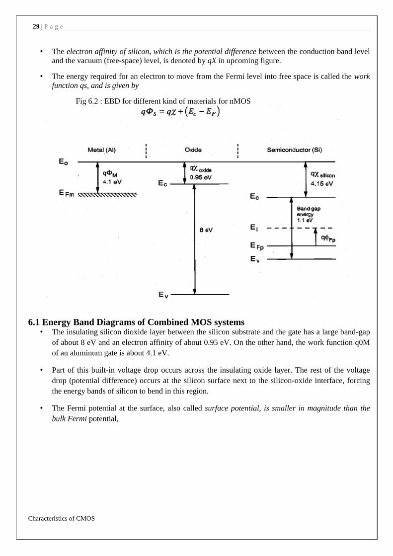
• The electron affinity of silicon, which is the potential difference between the conduction band level
and the vacuum (free-space) level, is denoted by qX in upcoming figure.
• The energy required for an electron to move from the Fermi level into free space is called the work
function qs, and is given by
Fig 6.2 : EBD for different kind of materials for nMOS
6.1 Energy Band Diagrams of Combined MOS systems • The insulating silicon dioxide layer between the silicon substrate and the gate has a large band-gap
of about 8 eV and an electron affinity of about 0.95 eV. On the other hand, the work function q0M
of an aluminum gate is about 4.1 eV.
• Part of this built-in voltage drop occurs across the insulating oxide layer. The rest of the voltage
drop (potential difference) occurs at the silicon surface next to the silicon-oxide interface, forcing
the energy bands of silicon to bend in this region.
• The Fermi potential at the surface, also called surface potential, is smaller in magnitude than the
bulk Fermi potential,
30 | P a g e
Characteristics of CMOS
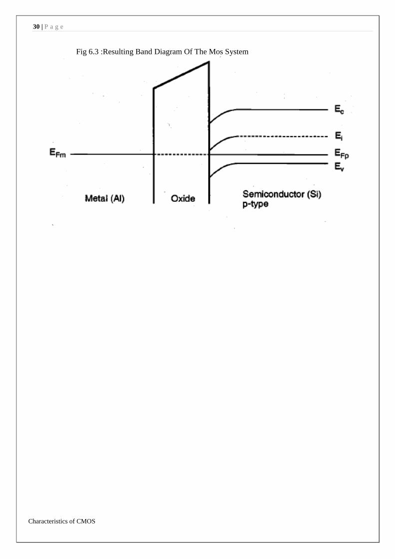
Fig 6.3 :Resulting Band Diagram Of The Mos System
31 | P a g e
Characteristics of CMOS
7. nMOS EXTERNAL BIASING • Assume that the substrate voltage is set at VB = 0, and let the gate voltage be the controlling
parameter.
• Depending on the polarity and the magnitude of VG, three different operating regions can be
observed for the MOS system:
– Accumulation
– Depletion, and
– Inversion.
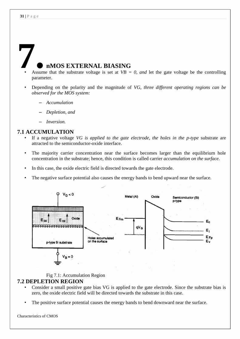
7.1 ACCUMULATION • If a negative voltage VG is applied to the gate electrode, the holes in the p-type substrate are
attracted to the semiconductor-oxide interface.
• The majority carrier concentration near the surface becomes larger than the equilibrium hole
concentration in the substrate; hence, this condition is called carrier accumulation on the surface.
• In this case, the oxide electric field is directed towards the gate electrode.
• The negative surface potential also causes the energy bands to bend upward near the surface.
Fig 7.1: Accumulation Region
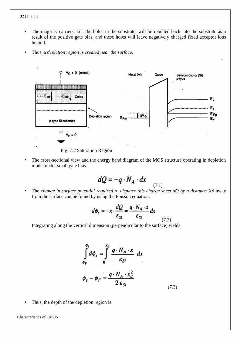
7.2 DEPLETION REGION • Consider a small positive gate bias VG is applied to the gate electrode. Since the substrate bias is
zero, the oxide electric field will be directed towards the substrate in this case.
• The positive surface potential causes the energy bands to bend downward near the surface.
32 | P a g e
Characteristics of CMOS
• The majority carriers, i.e., the holes in the substrate, will be repelled back into the substrate as a
result of the positive gate bias, and these holes will leave negatively charged fixed acceptor ions
behind.
• Thus, a depletion region is created near the surface.
Fig: 7.2 Saturation Region
• The cross-sectional view and the energy band diagram of the MOS structure operating in depletion
mode, under small gate bias.
(7.1)
• The change in surface potential required to displace this charge sheet dQ by a distance Xd away
from the surface can be found by using the Poisson equation.
(7.2)
Integrating along the vertical dimension (perpendicular to the surface) yields
(7.3)
• Thus, the depth of the depletion region is
33 | P a g e
Characteristics of CMOS
(7.4)
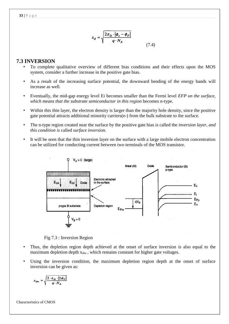
7.3 INVERSION • To complete qualitative overview of different bias conditions and their effects upon the MOS
system, consider a further increase in the positive gate bias.
• As a result of the increasing surface potential, the downward bending of the energy bands will
increase as well.
• Eventually, the mid-gap energy level Ei becomes smaller than the Fermi level EFP on the surface,
which means that the substrate semiconductor in this region becomes n-type.
• Within this thin layer, the electron density is larger than the majority hole density, since the positive
gate potential attracts additional minority carriers(e-) from the bulk substrate to the surface.
• The n-type region created near the surface by the positive gate bias is called the inversion layer, and
this condition is called surface inversion.
• It will be seen that the thin inversion layer on the surface with a large mobile electron concentration
can be utilized for conducting current between two terminals of the MOS transistor.
Fig 7.3 : Inversion Region
• Thus, the depletion region depth achieved at the onset of surface inversion is also equal to the
maximum depletion depth xdm , which remains constant for higher gate voltages.
• Using the inversion condition, the maximum depletion region depth at the onset of surface
inversion can be given as:
34 | P a g e
Characteristics of CMOS
8. pMOS modes of operation
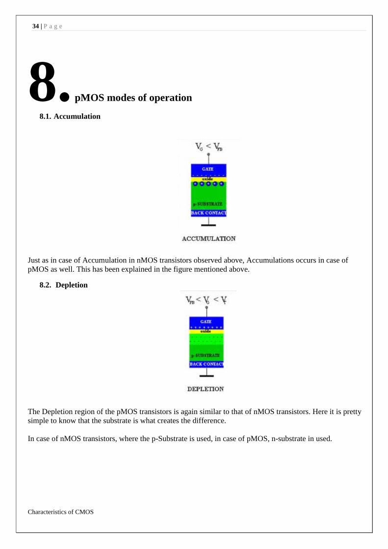
8.1. Accumulation
Just as in case of Accumulation in nMOS transistors observed above, Accumulations occurs in case of
pMOS as well. This has been explained in the figure mentioned above.
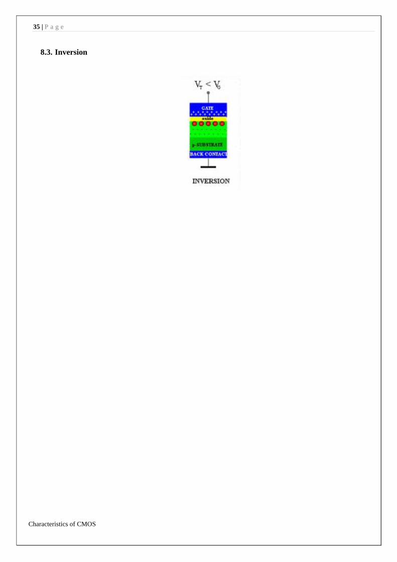
8.2. Depletion
The Depletion region of the pMOS transistors is again similar to that of nMOS transistors. Here it is pretty
simple to know that the substrate is what creates the difference.
In case of nMOS transistors, where the p-Substrate is used, in case of pMOS, n-substrate in used.
35 | P a g e
Characteristics of CMOS
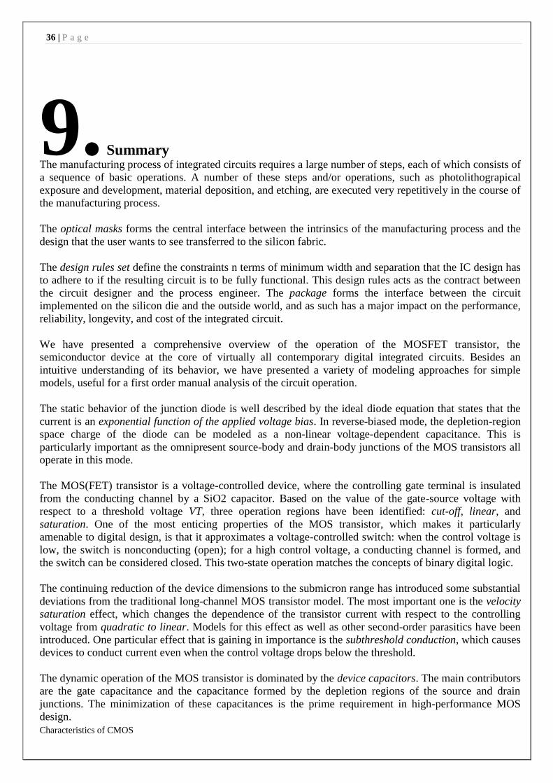
8.3. Inversion
36 | P a g e
Characteristics of CMOS
9. Summary The manufacturing process of integrated circuits requires a large number of steps, each of which consists of
a sequence of basic operations. A number of these steps and/or operations, such as photolithograpical
exposure and development, material deposition, and etching, are executed very repetitively in the course of
the manufacturing process.
The optical masks forms the central interface between the intrinsics of the manufacturing process and the
design that the user wants to see transferred to the silicon fabric.
The design rules set define the constraints n terms of minimum width and separation that the IC design has
to adhere to if the resulting circuit is to be fully functional. This design rules acts as the contract between
the circuit designer and the process engineer. The package forms the interface between the circuit
implemented on the silicon die and the outside world, and as such has a major impact on the performance,
reliability, longevity, and cost of the integrated circuit.
We have presented a comprehensive overview of the operation of the MOSFET transistor, the
semiconductor device at the core of virtually all contemporary digital integrated circuits. Besides an
intuitive understanding of its behavior, we have presented a variety of modeling approaches for simple
models, useful for a first order manual analysis of the circuit operation.
The static behavior of the junction diode is well described by the ideal diode equation that states that the
current is an exponential function of the applied voltage bias. In reverse-biased mode, the depletion-region
space charge of the diode can be modeled as a non-linear voltage-dependent capacitance. This is
particularly important as the omnipresent source-body and drain-body junctions of the MOS transistors all
operate in this mode.
The MOS(FET) transistor is a voltage-controlled device, where the controlling gate terminal is insulated
from the conducting channel by a SiO2 capacitor. Based on the value of the gate-source voltage with
respect to a threshold voltage VT, three operation regions have been identified: cut-off, linear, and
saturation. One of the most enticing properties of the MOS transistor, which makes it particularly
amenable to digital design, is that it approximates a voltage-controlled switch: when the control voltage is
low, the switch is nonconducting (open); for a high control voltage, a conducting channel is formed, and
the switch can be considered closed. This two-state operation matches the concepts of binary digital logic.
The continuing reduction of the device dimensions to the submicron range has introduced some substantial
deviations from the traditional long-channel MOS transistor model. The most important one is the velocity
saturation effect, which changes the dependence of the transistor current with respect to the controlling
voltage from quadratic to linear. Models for this effect as well as other second-order parasitics have been
introduced. One particular effect that is gaining in importance is the subthreshold conduction, which causes
devices to conduct current even when the control voltage drops below the threshold.
The dynamic operation of the MOS transistor is dominated by the device capacitors. The main contributors
are the gate capacitance and the capacitance formed by the depletion regions of the source and drain
junctions. The minimization of these capacitances is the prime requirement in high-performance MOS
design.
37 | P a g e
Characteristics of CMOS
References
[1.] CMOS: Digital Integrated Circuits- Mao Su Kang and Yusuf Leblebici [2.] E-Digital Integrated
[3.] Principles of Data Conversion System Design-Behzad Razavi
[4.] CMOS Integrated Analog-to-Digital and Digital-to-Analog Converters- Rudy J. van
[5.] CMOS Circuit Design, Layout, and Simulation- Bake Li Boyc
[6.] Design of Analog CMOS Integrated Circuits- Behzad Razavi