chapter 3thesis.library.caltech.edu/1685/4/03chapter3-experimental.pdf · this chapter briefly...
TRANSCRIPT

62
Chapter 3
Ultrafast Electron Crystallography:
Methodology and Apparatus

63
Introduction
The apparatus of ultrafast electron crystallography (UEC) was built for the studies
of condensed matter and surface assemblies (1, 2), on the basis of the experiences
accumulated through the construction of the first three generations for gas-phase
molecular studies in our group (3, 4). Conceptually, the UEC technique uses the similar
scheme of laser excitation (pump) and electron probing, in which the optical initiation
marks the zero of time. With the specimen mounted inside the chamber, its diffraction
pattern is digitally recorded. By varying the delay time between the arrival of the optical
and electron pulses on the surface of the specimen, diffraction snapshots at different times
are obtained; the diffraction patterns contain information about the structural evolution,
as a function of time, of the material under study. The analysis of diffraction feature
changes provides the temporal profiles for certain physical processes, as described in
Ch. 2. Finally, structural dynamics and an overall physical picture are obtained through
the correlation between these processes.
The UEC apparatus can be operated in the reflection or transmission detection
mode. Their experimental configurations are basically the same, except for a small
difference in that for transmission, an additional vertical sample holder is used to support
the thin specimens; the electron beam penetrates through a sample instead of being
scattered from a surface. This chapter briefly describes the parts that form the apparatus
and discusses about several topics in the experimental consideration. Details for the
construction of the instrument may be found in Ref. 2. A further development
implementing the scheme of pulse front tilting (5) was made by Dr. Peter Baum. Its
concept for resolving the temporal mismatch between the optical and electron pulses on
the specimen (thus improving the temporal resolution of UEC) is also summarized.

64
Fig. 1. UEC apparatus. Shown are the three UHV chambers and the two laser beams from
the femtosecond laser system for optical excitation and electron generation.
Apparatus of UEC
The UEC apparatus consists of a femtosecond laser system for generation of the
electron probe and optical initiating pulses; an assembly of ultrahigh vacuum (UHV)
chambers for diffraction, load lock (sample handling) and characterization; an electron
gun system in a high vacuum chamber; and a charged-couple device (CCD) camera
assembly for pattern recording (Fig. 1). The UHV environment is necessary for the
surfaces and interfacial assemblies that are sensitive to pressure as a result of their easy
deterioration caused by the bombardment or coverage of gas molecules. Manual and
pressurized gate valves (dark blue modules in Fig. 1) were installed for the separation
65
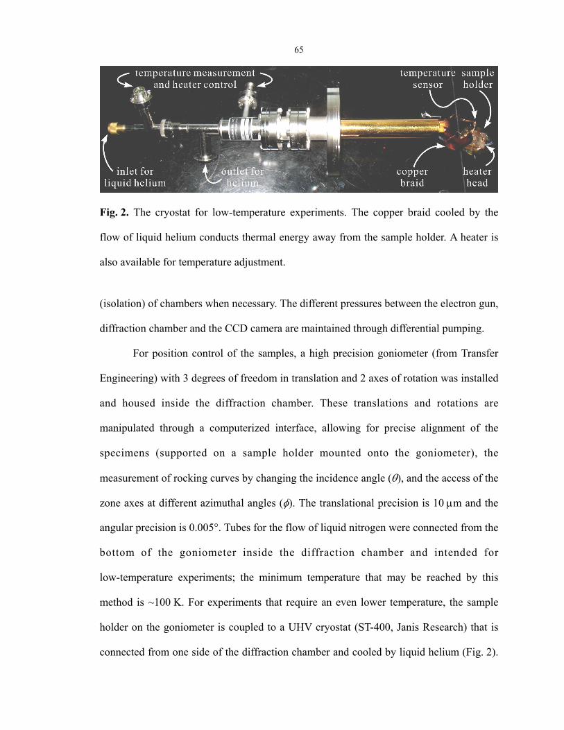
Fig. 2. The cryostat for low-temperature experiments. The copper braid cooled by the
flow of liquid helium conducts thermal energy away from the sample holder. A heater is
also available for temperature adjustment.
(isolation) of chambers when necessary. The different pressures between the electron gun,
diffraction chamber and the CCD camera are maintained through differential pumping.
For position control of the samples, a high precision goniometer (from Transfer
Engineering) with 3 degrees of freedom in translation and 2 axes of rotation was installed
and housed inside the diffraction chamber. These translations and rotations are
manipulated through a computerized interface, allowing for precise alignment of the
specimens (supported on a sample holder mounted onto the goniometer), the
measurement of rocking curves by changing the incidence angle (), and the access of the
zone axes at different azimuthal angles (). The translational precision is 10 m and the
angular precision is 0.005°. Tubes for the flow of liquid nitrogen were connected from the
bottom of the goniometer inside the diffraction chamber and intended for
low-temperature experiments; the minimum temperature that may be reached by this
method is ~100 K. For experiments that require an even lower temperature, the sample
holder on the goniometer is coupled to a UHV cryostat (ST-400, Janis Research) that is
connected from one side of the diffraction chamber and cooled by liquid helium (Fig. 2).

66
Fig. 3. Schematic of the femtosecond laser system and its integration into the UEC
apparatus. The arrangement of the beam paths is specifically for experiments that
consider the specimen excitation to be achieved by near-infrared 800-nm light pulses. A
capillary doser is connected to the top of the chamber for studies of molecular assembly.
A temperature of ≤20 K is readily achieved without too fast helium consumption. As for
experiments that require a temperature higher than the room temperature, the wires
installed under the goniometer head can heat the sample holder (up to ~500 K) through
the adjustment of the electric current; its influence on the electron beam direction is small
and, therefore, does not interfere with the recording of diffraction images.
The femtosecond laser system consists of an oscillator, an amplifier, and two
pump lasers (Fig. 3). The mode-locked Ti:sapphire oscillator (Tsunami, Spectra-Physics)
is pumped by a continuous-wave, diode-pumped Nd:YVO4 laser (Millennia Vs,
Spectra-Physics) with an average power of 5 W at 532 nm. The output of the oscillator is
femtosecond laser pulses centered at 800 nm, with a repetition rate of 80 MHz and a
pulse energy of 8 nJ. These pulses are amplified by a Ti:sapphire amplifier (Spitfire,
Spectra-Physics) pumped by a diode-pumped, Q-switched Nd:YLF laser (Evolution-30,
Spectra-Physics) whose repetition rate is 1 kHz and pulse energy is >20 mJ centered at
527 nm. The output of the amplifier is femtosecond pulses centered at 800 nm (1.55 eV),
67
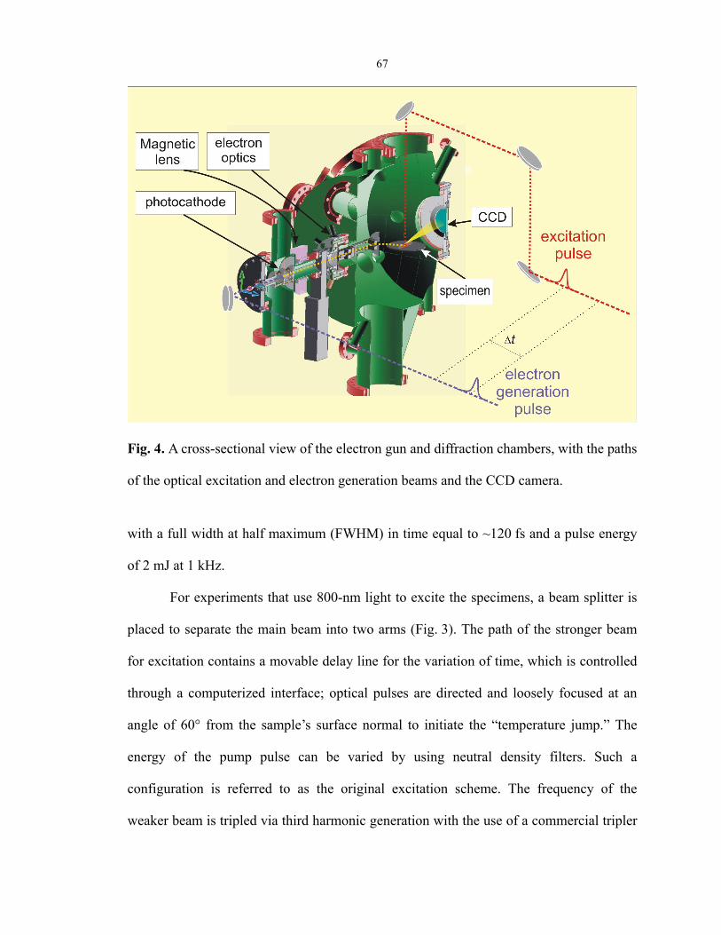
Fig. 4. A cross-sectional view of the electron gun and diffraction chambers, with the paths
of the optical excitation and electron generation beams and the CCD camera.
with a full width at half maximum (FWHM) in time equal to ~120 fs and a pulse energy
of 2 mJ at 1 kHz.
For experiments that use 800-nm light to excite the specimens, a beam splitter is
placed to separate the main beam into two arms (Fig. 3). The path of the stronger beam
for excitation contains a movable delay line for the variation of time, which is controlled
through a computerized interface; optical pulses are directed and loosely focused at an
angle of 60° from the sample’s surface normal to initiate the “temperature jump.” The
energy of the pump pulse can be varied by using neutral density filters. Such a
configuration is referred to as the original excitation scheme. The frequency of the
weaker beam is tripled via third harmonic generation with the use of a commercial tripler

68
(TP-1A, U-Oplaz Technologies). This ultraviolet beam at 266 nm (4.65 eV) is used to
generate ultrashort electron pulses through the photoelectric effect (see below). In regard
to experiments with 266-nm excitation, the beam splitter is placed after the whole
800-nm beam from the amplifier passes through the tripler, in order to separate a stronger
arm for initiation and a weaker one for electron generation; the rest of the beam paths
remain the same as the original excitation scheme at 800 nm.
Electron pulses are generated by the 266-nm beam back-illuminating the
photocathode (Fig. 4), which is made of a thin silver film (~45 nm in thickness) deposited
by the vapor deposition method on a sapphire window that is enclosed by a close-fitting
groove at the end of the stainless steel cathode set; see Figs. 3-4 and 3-5 in Ref. 4 for
illustration of the electron gun assembly. Before deposition of the silver film, the edge of
the sapphire window is first glued to the groove rim with the use of conductive silver
paint for the window’s immobility and good electric contact. The cathode set is connected
to a high voltage supply (FC60N2, Glassman High Voltage) through a vacuum
feedthrough, and the anode is grounded to the whole chamber system.
In our experiments, the typical pulse energy of the 266-nm beam for the electron
generation is on the order of sub-microjoule or below. It is focused on the photocathode,
and the number of photoemitted electrons in a pulse is in the range of several hundred to
few thousand (adjusted by varying the intensity of the ultraviolet beam with the use of
neutral density filters). The purpose of limiting the electron number is to maintain a
temporal width of several hundred femtoseconds to few picoseconds that is suitable for
the detection of ultrafast structural dynamics (6). The photoemitted electrons are
accelerated by a voltage of 30 kV in 3 mm, resulting in a de Broglie wavelength of
~0.07 Å. The electron pulses are focused by a magnetic lens and directed onto the

69
specimen after passing through a series of apertures and electrostatic deflection plates.
The incidence angle of electrons is typically below 5°. Without hitting any object, the
direct beam has a diameter (spatial FWHM) of ~200 m (about 4 to 5 pixels) on the CCD
screen, which becomes a time-independent contribution to the width of diffraction. The
resulting average (current) flux of electrons is relatively small, on the order of
0.1–5 pA/mm2 depending on the probing geometry. Therefore, no electron damage,
modification, or charging of the specimens is observed for most experiments.
The CCD assembly (Fig. 2.6 in Ref. 2) has a low noise level and contains an
image intensifier (V5181U-06, Hamamatsu), which enables single-electron detection.
The camera (Princeton Instruments PI-SCX:1300/W, Roper Scientific) records 16-bit
digital images through a computerized interface, with an intensity range from 0 to 65535
(= 216–1). The largest image range has 1340 pixels in the horizontal direction and
1300 pixels in the vertical; the measured pixel size is 44.94±0.25 m in both directions.
With a camera length (from the specimen to the phosphor screen) of ~16.8 cm, each pixel
represents a scattering angle of 0.268 mrad, or 0.0240 Å–1 in the reciprocal space
according to the definition of s = (4/)sin(/2). Therefore, with the help of curve fitting,
the resolution of our apparatus reaches <0.01 mrad, i.e., few percent of a pixel or
equivalent quantities; one example may be seen in Fig. 3b of Ch. 5. To block the
undiffracted electrons (the direct beam) from reaching the phosphor screen and saturating
the image intensity, a grounded, movable copper tube that serves as the beam trap is used
during the recording of diffraction patterns.
The Scheme of Pulse Front Tilting
The most important factor that limits the temporal resolution of UEC, particularly

70
Fig. 5. (a) Mismatch between the arrival times of the nontilted initiating and electron
pulses. The resulting temporal resolution is on the order of 10 ps. (b) The scheme of pulse
front tilting. The extent of the pulse tilt is solely determined by the ratio of the speed of
light to that of electrons.
in reflection experiments, is the mismatch between the optical initiating and electron
probe pulses in the interaction region on the specimen. Even if the two pulses have
femtosecond temporal widths, given the fact that electrons graze at a small incidence
angle and probe the photoexcited region with a longitudinal dimension (l) on the order of
1 mm, the mismatch between the arrival times of the optical and electron pulses would be
on the order of 10 ps for 30-keV electrons, whose velocity is 1/3 the speed of light (c)
(Fig. 5a). Improving the temporal resolution in this excitation scheme requires reduction
of the interaction region along the electron propagation direction, typically by limiting
the useful sample region (see Ch. 4 and Ref. 7). However, a natural consequence of this
method is a substantial decrease of diffraction intensity in a given exposure time;
unavoidable prolonged experiments may lead to other undesirable issues such as the
long-term instability and sample deterioration.

71
The scheme of pulse front tilting can be implemented to solve the aforementioned
temporal mismatch (5). As shown in Fig. 5b, the intensity front of the initiating pulse
needs to be tilted by an angle of ≈ 72° to have the synchrony of the two pulses’ arrival
at every point of the interaction region on the specimen, because the ratio of the traveling
speed of light to that of 30-keV electrons is ~3. Experimentally, a grating is used as the
diffractive element for 800-nm light to introduce the angular dispersion and, concurrently,
the traveling path difference necessary for pulse tilting. In addition, a spherical mirror is
placed after the grating to gather the different spectral components originated and then
dispersed from the same part of the spatial profile to coincide at the same corresponding
point on the specimen; this method is optical imaging and effectively reconstructs the
femtosecond optical pulse according to the energy–time uncertainty relation. The
resulting reduction in time spread was confirmed to be better than 25 fold (5).
In Ch. 6, the application of the pulse tilting scheme proves to be critical to the
resolution of ultrafast structural dynamics on the femtosecond time scale. The number of
electrons per pulse is reduced to as low as ~500 in that study to minimize the
space-charge effect (6) and, at the same time, maintain a reasonable duration for the
experiments. With such a low flux, the electron pulse width of 322 ± 128 fs has been
measured in situ at a streaking speed of 140 ± 2 fs/pixel (8). Although the overall
temporal resolution is determined by convolution of the involved optical and electron
pulses with any residual spread from pulse tilting, its improvement to ~400 fs is far better
than the 20-ps spread estimated from the sample dimension of ~2 mm probed in the
electron propagation direction. The pulse tilting scheme is also applied to the studies
reported in Chs. 5, 7 and 8 and in Ref. 9. Particularly for the latter two cases, the much
improved temporal resolution is critical to the new discoveries.

72
Fig. 6. The original excitation scheme and measurement of the FWHM. (a) The loosely
focused optical beam impinges on the specimen at a specific incidence angle. (b) The
width measurement determines the distance between the points indicates by the black
arrows, which is w/cos30° from the trigonometric relationship.
Experimental Consideration in UEC
A. Concerning Initiating Pulses and Optical Excitation
The first important thing to consider about the initiating pulse is the photon energy.
Because ultrafast change of a specimen is initiated by photoexcitation in UEC, dynamics
studies can only be made for materials that absorb the initiating pulses, whether the
absorption is achieved through a one-photon process or through a multi-photon one. Thus,
metallic materials and semiconductors with a band gap smaller than 4.65 eV may be
investigated using the current laser system; the following chapters give examples for
different types of substance. For insulating materials, although energetically possible,
simultaneous absorption of two 266-nm photons for photoexcitation would be difficult to
achieve due to the weak ultraviolet beam. Two other issues that may also restrict the UEC
study of an insulator are the accompanying photoemission (which can affect the electron

73
beam path and probing) and surface charging (as a result of poor electric conduction).
The next important thing is the laser fluence on the specimen. Assuming that the
beam profile is of a Gaussian form and its projection on the surface is circular, the peak
fluence at the center is F(r=0) = E0·4 ln2/(w2), where E0 is the integrated pulse energy
and w is the spatial FWHM. To define the average fluence (Favg) for such a beam, we
consider the illuminated area to be 2 times the FWHM range, which gives
Favg = 2E0/(w2) to be smaller than the peak value, F(r=0), but larger than half of it. This
estimation is reasonable because the electron probed region (a stripe of 200 m by few
millimeters extending in the electron propagation direction) is intended to be narrower
than and coincide with the intense part of the laser footprint in the horizontal direction.
Therefore, the task of the estimation of fluence becomes measurement of the FWHM of
the laser footprint.
The original excitation scheme produces an elliptical illuminated region on the
specimen, as shown in Fig. 6. In the width measurement, the rod part of a needle was
used as a blade to block the passing of the laser beam toward a photodiode, by which the
intensity was recorded. According to the top view illustrated in Fig. 6b, the edge of the
rod moved in the vertical direction, first intercepting with the beam from the bottom
(indicated by the lower black arrow) and then totally blocking it (indicated by the upper
black arrow); the rod diameter was larger than the FWHM of the beam. Thus, the
recorded intensity curve was in the form of an error function, whose derivative was
Gaussian with a FWHM equal to w/cos30° (Fig. 6b). A typical value for w is 0.726 mm,
and hence the corresponding temporal resolution is about 7 ps.
In the scheme of pulse front tilting, the initiating pulses impinge perpendicularly
on the specimen, and the horizontal and vertical widths of the stretched elliptical footprint

74
were measured with the help of an auxiliary camera. During the measurement, the laser
intensity was attenuated such that the peak fluence on the surface appeared to be just
saturated in the screenshot captured by the auxiliary camera. The horizontal and vertical
intensity profiles of the footprint were fitted to determine the (scaled) widths. Real
FWHM values were obtained by multiplying the widths on the screen with the
conversion factor (i.e., the ratio of a length in reality to its appearance in the screenshot),
through the help of an object whose size was known. The common FWHM region used is
0.24 mm by 3 mm, which is large enough to make the electron probed region match with
the higher fluence part after appropriate alignment (see below).
B. Concerning Electron Pulses and Probing
The important properties of an electron pulse include the number of electrons, its
temporal width, and the energy and angular spread. The energy uncertainty is on the order
of 10 V, given the output steadiness of the high voltage supply (<0.02% of rated voltage,
60 keV) and the excess energy above the work function of silver (tenths of a volt at most).
A crude estimation of the electrons’ angular spread in a pulse is given by the ratio of the
initial size of photoemitted electrons (restricted by a pinhole of 150 m) to the distance to
reach the magnetic lens (~5 cm), or by the ratio of the pulse diameter on the CCD screen
(~200 m) to the traveling distance of electrons from the magnetic lens (67 cm), which is
on the order of 0.1 to 1 mrad. Moreover, the spatial width of the electron beam also
contains a small contribution from the little random jitter in the electron propagation
direction around the average one. These factors consequently affect the coherence length
seen by the electrons (Ch. 2).
Below the saturation level, the total intensity (above the noise level) recorded by
the CCD camera is linearly dependent on the number of electrons that reach the phosphor

75
screen, at a given voltage for the image intensifier. Hence, the average electron number
per pulse can be obtained by recording many single-pulse images, fitting the profiles to
extract their total intensities, widths and positions, and dividing the intensity values by a
conversion factor. This factor was previously obtained by counting the total intensity of
each single-electron or few-electron event recorded in (at least) hundreds of images
without magnetic lens focusing, and fitting the histogram of intensity to the Poisson
distribution. The electron-generating 266-nm beam needed to be strongly attenuated such
that only several electrons were generated in a pulse, with clear angular separation to
make the counting process easier.
The relationship between the electron density in a pulse and its temporal width
has been established by performing the streaking experiment (1, 8). Typically, for an
increment of a thousand electrons per pulse, the width is increased by ≥1 ps. Thus, the
major limitation of UEC’s temporal resolution is the mismatch between the electron and
optical pulses, and its solution by using the scheme of pulse front tilting was described
earlier. During the experiments, diffraction patterns without laser excitation are recorded
for the characterization of the specimens, and their differences are examined to see if the
effect of electron charging, damage or modification exists as a result of constant electron
bombardment. Our experiences show that the pulsed electron probing and existence of
the bulk part of metallic or semiconducting samples (attached to the holder by conductive
copper tape) greatly reduce the chance to encounter these undesirable issues. In contract,
the surface morphology that contains sharp tips can be problematic because they may act
as photoemitting sources or charge accumulation points, especially with laser excitation.
C. Aligning the Footprints of the Optical and Electron Beams
The major difficulty for the alignment of the interaction region is that the electron

76
Fig. 7. Schematic for preliminary alignment of the optical and electron pulses. The edge
of a substrate (e.g., sapphire) serves as the guideline.
Fig. 8. Fine adjustment for the overlap of the laser and electron footprints. (a) An image
taken by the auxiliary camera shows the specimen and the laser footprint. (b) Slight
differences in the footprint overlap (upper panels) lead to different results in the
diffraction difference images (lower panels).

77
beam footprint on the specimen is not visible. A method that utilized the tip of a stainless
steel needle to intercept with the electron beam path was developed for the original
excitation scheme (2). However, the alignment can be achieved by another method, with
the use of a substrate that has straight and clear edges (e.g., 0.5-mm thick sapphire) and
an auxiliary camera to monitor the substrate and the laser footprint (Fig. 7). For
preliminary alignment, the substrate is rotated azimuthally such that one of its edges is
approximately parallel to the electron path; the height of the goniometer is adjusted so
that the electron beam can be blocked by the substrate but not by the sample holder. By
moving the goniometer horizontally and monitoring the electron pulses in the CCD
images, the edge can serve as a visual guideline for the electron beam path. The laser
footprint is directed to match with the edge in the screenshot of the auxiliary camera
when the electron beam is half-blocked.
For accurate alignment, the horizontal deflection voltage for electrons is to be
adjusted. In the original excitation scheme, a small change of a few volts may be
necessary for the observation of largest diffraction difference (referenced to the negative
time frame) at positive delay times, which signifies a well-defined interaction region. In
the case of the pulse tilting scheme, due to the comparable widths of the laser and
electron footprints used, an imperfect alignment on the specimen in the horizontal
direction may lead to horizontal asymmetry in the diffraction difference. An example is
provided in Fig. 8, which shows the diffraction difference images obtained from a
gallium arsenide sample with different overlaps of the footprints. This phenomenon can
be related to both the small change in the Bragg condition and electron refraction because
of the expanded lattice at positive times and the corresponding tilt of the surface normal
for the wing parts of the optical excitation (Fig. 8b, left and right). With regard to the

78
vertical alignment, the height of the specimen is slightly adjusted to obtain the largest
diffraction difference. If the sample has a dimension of ~1 to 3 mm, such an adjustment is
expected to be achieved easily.
References:
1. C.-Y. Ruan, F. Vigliotti, V. A. Lobastov, S. Chen, A. H. Zewail, Proc. Natl. Acad.
Sci. USA 101, 1123 (2004).
2. S. Chen, Ph.D. thesis, California Institute of Technology (2007).
3. J. C. Williamson, Ph.D. thesis, California Institute of Technology (1998).
4. R. Srinivasan, Ph.D. thesis, California Institute of Technology (2005).
5. P. Baum, A. H. Zewail, Proc. Natl. Acad. Sci. USA 103, 16105 (2006).
6. A. Gahlmann, S. T. Park, A. H. Zewail, Phys. Chem. Chem. Phys. 10, 2894 (2008).
7. F. Vigliotti, S. Chen, C.-Y. Ruan, V. A. Lobastov, A. H. Zewail, Angew. Chem. Int.
Ed. 43, 2705 (2004).
8. V. A. Lobastov et al., in Ultrafast optics IV, F. Krausz, G. Korn, P. Corkum, I. A.
Walmsley, Eds., vol. 95 of Springer series in optical sciences (Springer, New York,
2004), pp. 419-435.
9. F. Carbone, P. Baum, P. Rudolf, A. H. Zewail, Phys. Rev. Lett. 100, 035501 (2008).