chapter 5 design of third order and delay interpolator...
TRANSCRIPT

70
CHAPTER 5
DESIGN OF THIRD ORDER AND DELAY
INTERPOLATOR BASED SELF BIASED PLL
This chapter discusses the other attempted modifications on the
traditional self biased PLL. The modification of the second order PLL into
third order PLL is discussed first. The architecture of the third order PLL, and
the design of its loop parameters from the stability considerations of the PLL
is discussed. The results are presented showing the capability of the third
order PLL to improve jitter performance as well as settle fast with minimum
capture transients. Following the discussion on the third PLL is the discussion
on delay interpolator VCO based PLL that retains the swing of the self biased
PLL, which otherwise varies with control voltage. Unlike the traditional self
biased PLL, this architecture is differential, hence its potential to reject
systematic noise is also discussed. The simulation results of this delay
interpolator based PLL is finally presented and the performance is compared
with the reference PLL.
5.1 DESIGN OF THIRD ORDER PLL
A generic third order PLL architecture can be derived from a
general second order PLL by introducing an additional transconducatnce Gm
stage and a first order loop filter section as described in Donald Stephens R.
(1997). The architecture of this third order PLL is shown in Figure 5.1.

71
Figure 5.1 Block Diagram of a Generic Third Order PLL
This generic architecture has been modified to adopt the salient
features of a traditional self biased adaptive bandwidth second order PLL as
follows. The VCO chosen is a ring oscillator with symmetric load delay
elements along with appropriate bias generators. These bias generators
provide the required biases for the delay elements, the Charge Pump (CP) and
the transconductance Gm stage. The resistors R shown in Figure 5.1
associated with the first and second loop filters are realized using separate
charge pumps, and these are also biased from the bias generators. The
modified third order self biased adaptive bandwidth PLL system functionality
and the selection of the loop parameters of the modified system are explained
in the following sections.
5.1.1 Third Order PLL System Description
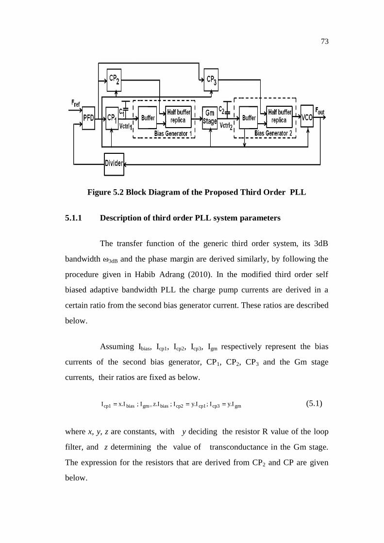
The functional blocks of the third order self biased adaptive
bandwidth PLL are shown in Figure 5.2. The system comprises of a Phase
Frequency Detector (PFD), three charge pumps CP1, CP2, CP3, loop filter
capacitances C1,C2, a Gm stage, two bias generators , a VCO, and a divider.

72
The PFD employed is a tristate PFD that compares the reference
signal Fref and the feed back clock signal from the divider. The pulses
generated from the PFD drives the charge pumps CP1, CP2, and CP3. Here,
CP1 is used as a charge pump to drive C1 and CP2 and CP3 are used for
realizing the resistors for the loop filter sections. The first bias generator
buffers the integrated voltage from the capacitor C1 and combines the current
from CP2 to derive an output voltage Vctrl1. This output in turn drives the Gm
stage and which in turn proportionately drives the capacitor C2. Next, the
second bias generator buffers the integrated voltage from C2 and combines the
current from CP3 to generate Vctrl2 which finally controls the VCO to
generate the required VCO frequency.
The bias currents for CP1, CP2, CP3 and Gm stage are derived from
the second bias generator which also delivers the bias current to the delay
elements in the VCO. The charge pump and Gm stage bias currents are
adjusted as the VCO operating frequency is varied. Since the bias current in
CP2 and CP3 are also adjusted, the resistors vary accordingly. As the charge
pump currents and the associated resistances change with operating
frequency, the system loop bandwidth tracks the reference frequency as in the
original work of John Maneatis (1996). The phase margin also gets adjusted
to remain constant over the entire operating frequency range.
73
Figure 5.2 Block Diagram of the Proposed Third Order PLL
5.1.1 Description of third order PLL system parameters
The transfer function of the generic third order system, its 3dB
bandwidth 3dB and the phase margin are derived similarly, by following the
procedure given in Habib Adrang (2010). In the modified third order self
biased adaptive bandwidth PLL the charge pump currents are derived in a
certain ratio from the second bias generator current. These ratios are described
below.
Assuming Ibias, Icp1, Icp2, Icp3, Igm respectively represent the bias
currents of the second bias generator, CP1, CP2, CP3 and the Gm stage
currents, their ratios are fixed as below.
gmcp3cp1cp2biasgmbiascp1 y.II;y.II;z.II;x.II (5.1)
where x, y, z are constants, with y deciding the resistor R value of the loop
filter, and z determining the value of transconductance in the Gm stage.
The expression for the resistors that are derived from CP2 and CP are given
below.

74
bias8KI
y=R (5.2)
The ratio of the charge pump currents and the expressions for the
resistors from Equation (5.1) and (5.2) are applied in the expressions for 3dB
and the phase margin that are derived in Habib Adrang et al (2010). These
expressions are reproduced below.
)RG( mKIR
= VCOcp13dB (5.3)
Here KVCO is the gain of the VCO in the third order PLL.
2KIR
= VCOcp13dB (5.3)
The phase margin of the third order PLL is given below.
3dB11 RC2tan90PM (5.4)
The ratio of 3dB to reference frequency ratio ref expressed using the factors
x, and z, is derived similar to the procedure used in John Maneatis (1996), and
is given below .
216
zx2y
ref3dB = (5.5)
From the above, it can be observed that the ratio remains constant
and depends only on the ratio of currents.
Similarly, the phase margin is derived using the factors x, y and z
similar to the procedure employed in John Maneatis (1996) and is given
below

75
B
13
1CN16Czxy
2tan90PM (5.6)
where C1 represents the LPF capacitance. C2 (of Figure 5.2) is chosen to be of
the same value as C1. The effective capacitance CB is obtained from the
oscillator, and N is the prescalar division factor. From Eqn.6, it can be
observed that the phase margin is dependent on the ratio of capacitances,
therefore it will be a constant for the entire capture range of the third order
PLL.
From Equation (5.5) and (5.6) it can be noted that the 3dB to ref
and phase margin can be independently chosen since 3dB to ref factor is
independent of C1 , and C1 can then be chosen for a required phase margin
without influencing 3dB to ref. This permits the independent control of
settling time and capture transients in the third order PLL.
As per Equation (5.3), the 3dB of the third order PLL is extended by
the factor GmR, when compared with the traditional second order PLL, this
can thus help the system to settle fast. With the extension in bandwidth, the
phase margin of the third order PLL is also observed to get increased as per
Equation (5.4), this can permit the system to settle with minimum capture
transients and improve jitter performance.
5.1.3 Proposed PLL Design Specification and Simulation Results
The system is designed with the following specifications. The VCO
circuit is designed for a frequency range of 500MHz to 3GHz. The prescalar
divide ratio N is chosen as 16. The loop parameter constants x, y and z values
are chosen depending on the required PM and the 3dB to ref ratio. The value
of C1 is chosen as 100pF and the effective capacitance CB obtained from VCO

76
equals 0.248pF. With C1 chosen to be a larger and a circuit realizable value,
to maximize phase margin and the x, y and z values were chosen such that it
can give reduced settling time and minimum overshoot/undershoot transients.
The system stability conditions and step response were determined
using Matlab. The circuit was deigned in 0.18 m CMOS process UMC
technology library. The simulations were carried out using Cadence Spectre
tool.
Inorder to perform a comparative study the traditional second and
third order self biased adaptive bandwidth PLL has been designed with
similar functional block specifications. The values chosen for the factor x, y
defined in Equation (5.1) remains the same for both the cases. The values for
x and that of y is chosen as 0.2 and 5 respectively.
With the above constants, the loop bandwidth n to ref ratio in the
second order system turns out to be 1/26, and the damping factor was found
to be 3.
The step response of the third order self biased adaptive bandwidth
PLL for the chosen x, y and for three sets of z values were computed using
Matlab. The resulting plots are given in Figure 5.3. The third order PLL step
response plot that corresponds to a PM of 40 , 58 and 80 was obtained by
choosing z as 0.25, 0.35 and 0.6 respectively. Finally the value of z is chosen
as 0.6 since it gives a realizable circuit implementation of the Gm stage to
obtain a transconductance value of the stage as 630 S. With this chosen z
value, the phase margin of the third order PLL was calculated using Equation
(5.6) and was found to be 80 . Further for this case, it may be also be clearly
seen from the plot that the settling time, undershoot/overshoot happened to be

77
the least in comparison with the step responses corresponding to the phase
margin of 40 and 58 .
Figure 5.3 Step Response of the Third Order PLL
Having derived the system level specifications using Matlab, the
circuit simulations were next carried out for both the second and the third
order system. The proportional charge pumps CP1 and CP2 were replaced by
appropriate value of resistance for the sake of simplicity. This is done to
verify the circuit realization of mathematical modeling of third order PLL.
The VCO operating frequency range is shown in Figure 5.4, and
the plot shows a linear operating range from 500MHz to 3GHz with a gain of
3.3GHz/V. The capture range of the resulting third order PLL was observed
to be from 1GHz to 2.72GHz.

78
Figure 5.4 VCO Gain of the Third Order PLL
A comparison of the control voltage transients for the second and
third order systems at 2.4GHz output frequency (with a step frequency of
700MHz) is shown in Figure 5.5. It can be observed that the third order PLL
while acquiring the final frequency shows negligible capture transients with
fast settling characteristic when compared with the second order PLL. The
second order PLL acquires within 2% of its final frequency after 190ns
(29 reference clock cycles) whereas the third order PLL acquires similarly
after 111ns (17reference clock cycles), showing 40% improvement in its
settling time.

79
Figure 5.5 Comparison of Control Voltage Transients of the Second and Third Order PLL at 2.4GHz
The jitter performance of both the PLLs at 2.4 GHz is shown in
Figure 5.6 by means of an eye diagram. The peak to peak jitter measured from
the eye diagram is 16.6ps for the second order PLL and is found to be 8.7ps
for the third order PLL. Thus the third order PLL shows 48% improvement in
its jitter performance.
Figure 5.6 Jitter Comparison at 2.4GHz
80
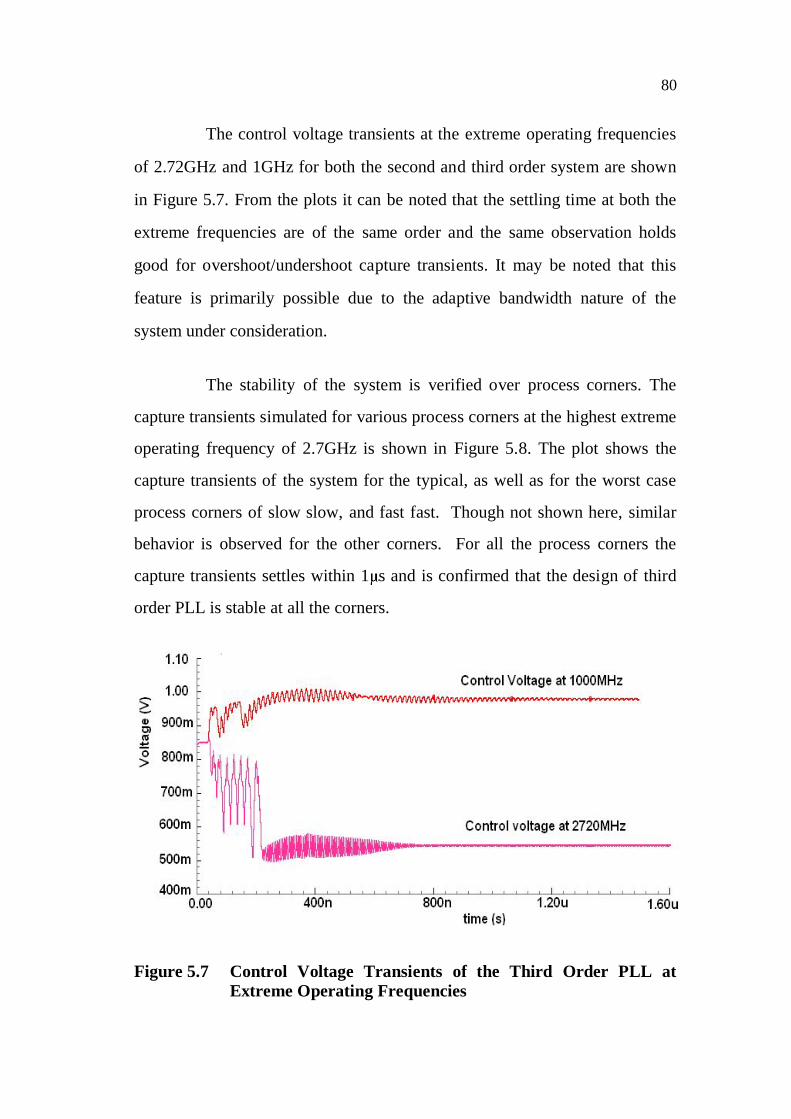
The control voltage transients at the extreme operating frequencies
of 2.72GHz and 1GHz for both the second and third order system are shown
in Figure 5.7. From the plots it can be noted that the settling time at both the
extreme frequencies are of the same order and the same observation holds
good for overshoot/undershoot capture transients. It may be noted that this
feature is primarily possible due to the adaptive bandwidth nature of the
system under consideration.
The stability of the system is verified over process corners. The
capture transients simulated for various process corners at the highest extreme
operating frequency of 2.7GHz is shown in Figure 5.8. The plot shows the
capture transients of the system for the typical, as well as for the worst case
process corners of slow slow, and fast fast. Though not shown here, similar
behavior is observed for the other corners. For all the process corners the
capture transients settles within 1 s and is confirmed that the design of third
order PLL is stable at all the corners.
Figure 5.7 Control Voltage Transients of the Third Order PLL at Extreme Operating Frequencies

81
Figure 5.8 Control Voltage Transients of the Third Order PLL at Process Corners
Table 5.1 Performance Comparison at operating frequency of 2.7GHz
Performance Parameters Second order PLL Proposed third order PLL
VCO operating range (MHz) 500 to 3000 500 to 3000
Capture range (MHz) 800 to 2700 1000 to 2700
RMS Jitter (ps) (UI)
3.1(0.84)
1.1(0.3)
Settling time ( s) 0.19 0.19
Peak Undershoot magnitude (MHz)
Undershoot in terms of control voltage transient(mV)
557
170
0.023
0.69
Peak power (mW) 36 40
The performance comparison of the proposed third order PLL with the second
order PLL designed in the present work is shown in Table 5.2 at the extreme
highest operating frequency of 2.7GHz. The third order PLL shows better

82
jitter performance of about 64% when compared with the second order PLL.
The third order system also shows negligible overshoot under shoot capture
transients without any degradation in its settling time when compared with the
second order counterpart. The performance improvement thus obtained in the
third order loop is with less additional power consumption than the traditional
second order PLL which is about 11% at 2.7GHz .
5.2 DESIGN OF DELAY INTERPOLATOR BASED SELF
BIASED PLL
In the traditional self biased PLL, the VCO swing depends on
operating frequencies that gets progressively reduced as the frequency
reduces and degrades the jitter considerably. The traditional self biased PLL
suitably modified to incorporate the delay interpolator VCO scheme proposed
by Seema Butala Anand et al (2001) that operates with a constant swing, but
without the benefits of supply noise immunity and loop bandwidth adaptivity.
Moreover, this VCO also operates with differential control voltage and thus
minimizes the impact of the deterministic noise generated within the circuit.
This work thus adapts the delay interpolator based VCO to the traditional self
biased PLL scheme in order to derive the benefits of both the schemes.
The modified system functionality and the adaptation of the delay
interpolator VCO to the self biased PLL scheme is discussed. Following that
is the discussion of detailed simulation results and overall system
performance comparison with the traditional self biased PLL.
5.2.1 Adaptation of Delay Interpolator VCO to the Self Biased PLL
The modified block diagram of the self biased PLL adopting delay
interpolation principle is shown in Figure 5.9. The functional blocks of the

83
proposed PLL consists of Phase Frequency Detector (PFD), charge pump
circuit CP, Loop Filters (with capacitor C and resistor R), delay interpolator
VCO and prescalar. In this proposed PLL except the VCO architecture all
other functional blocks remains the same as described in John Maneatis G.
(1996). The modified VCO functionality is based on the delay interpolator
architecture Seema Butala Anand et al (2001). The bias generator of the delay
interpolator VCO is modified from the traditional self biased VCO to derive
the required bias voltages from the differential control voltages to bias the
delay elements as well as the charge pump circuits.
Figure 5.9 Block Diagram of Self Biased PLL
The traditional self biased VCO employed by John Maneatis G.
(1996) with single ended control voltage is modified to delay interpolator
based VCO with differential control voltage, while the salient features
required for static and dynamic supply rejection characteristics of the
traditional self biased PLL are preserved. The architecture of the modified
VCO is shown in Figure 5.10 that consists of a bias generator stage (Bias
Gen) and a ring oscillator stage. The ring oscillator is designed with four
delay elements. The bias generator stage provides the appropriate bias

84
voltages Vbp, Vbp_cons, Vbn_cons, Vbn_slow, Vbn_fast to the delay elements. The
delay element architecture is very similar to the one employed in Seema
Butala Anand et al (2001) except that the resistive load is replaced by the
symmetric load proposed of John Maneatis G. (1996) and this in turn behaves
as a linear resistance for the entire frequency range of operation and achieves
dynamic supply noise rejection. The circuit schematic of the delay element
consisting of a slow path and a fast path is shown in Figure 5.11. As with the
architecture in Seema Butala Anand et al (2001), the buffer stage delay in the
slow path is maintained constant, independent of the control voltage whereas
the inverting stage delay in the slow path is controlled by Vbn_slow derived
from Vctrl- in the bias generator. The inverting stage delay in the fast path is
controlled by Vbn_fast generated from Vctrl+ in the bias generator. In the
symmetric load, the current steered by Vbn_slow in the slow path and the current
steered by Vbn_fast in the fast path are summed up. This summed up current Iss
stays constant and maintains a constant swing at the output node as in Seema
Butala Anand et al (2001).
Figure 5.10 Functional Block Diagram of the Proposed Self Biased VCO

85
5.2.2 Design of VCO
The gain KVCO of the proposed VCO is derived from the delay
contributed by the individual delay element stages and is described as below.
The delay tp contributed by a single delay element is derived from its RC
equivalent model given in Figure 5.12, and is expressed in Equation (5.7-
5.10) below.
tp = 0.692.n.(Kfast fast + Kslow slow). (5.7)
Kfast + Kslow = 1 (5.8)
fast = Rfast CL (5.9)
slow = (Rcons + Rslow) CL + Rcons Ccons (5.10)
Figure 5.11 Circuit Diagram of the Modified Delay Element

86
Figure 5.12 RC Equivalent Model of a Single Delay Element
In Equation (5.7) fast, slow are respectively the time constants
determined by the fast and slow paths. The coefficients Kfast and Kslow defined
in Equation (5.7) are the ratio of the current steered into slow path and fast
path of the inverting stages with the total bias current Iss and satisfies the
relation as given in Equation (5.8).
In Equation (5.9), the resistance Rfast is derived from the inverting
stage in the fast path and CL is the load capacitance at the output node of the
delay element stage. In Equation (5.10), Rcons is the resistance derived from
the constant delay buffer stage in the slow path, Ccons is the load capacitance
at the output node of the constant delay buffer in the slow path. Rslow is the
resistance obtained from the inverting stage in the slow path.
The resistance Rslow and Rfast are derived from the symmetric load
biased by Vbp. The resistance thus obtained is expressed below.
)VV(IK.21R,R
Tbpsspslowastf (5.11)

87
Here Kp represents device transconductance K (W/L), K denotes
process transconductance parameter and (W/L) denotes the aspect ratio of the
transistors employed in the symmetric load.
The resistance Rcons is similarly derived from the symmetric load
that is biased by Vbp_cons. The resistance thus obtained is expressed as below.
)VV(IK.21R
Tconsbpconscons_pcons (5.12)
Here Kp_cons is the device transconductance of the symmetric load.
Icons and Vbp_cons are derived from a constant bias voltage in the bias generator.
The VCO frequency is thus controlled by the time constants fast
and slow and the coeffecients kfast and Kslow and is given as below.
Fout = 2. n. K . + 2. n. K . _ ( )+ ( )
(5.13)
Figure 5.13 Circuit Schematic of Bias Generator
88
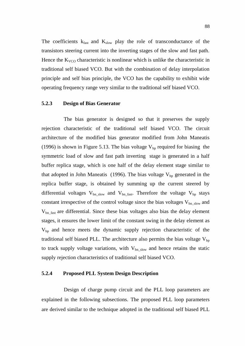
The coefficients kfast and Kslow play the role of transconductance of the
transistors steering current into the inverting stages of the slow and fast path.
Hence the KVCO characteristic is nonlinear which is unlike the characteristic in
traditional self biased VCO. But with the combination of delay interpolation
principle and self bias principle, the VCO has the capability to exhibit wide
operating frequency range very similar to the traditional self biased VCO.
5.2.3 Design of Bias Generator
The bias generator is designed so that it preserves the supply
rejection characteristic of the traditional self biased VCO. The circuit
architecture of the modified bias generator modified from John Maneatis
(1996) is shown in Figure 5.13. The bias voltage Vbp required for biasing the
symmetric load of slow and fast path inverting stage is generated in a half
buffer replica stage, which is one half of the delay element stage similar to
that adopted in John Maneatis (1996). The bias voltage Vbp generated in the
replica buffer stage, is obtained by summing up the current steered by
differential voltages Vbn_slow and Vbn_fast. Therefore the voltage Vbp stays
constant irrespective of the control voltage since the bias voltages Vbn_slow and
Vbn_fast are differential. Since these bias voltages also bias the delay element
stages, it ensures the lower limit of the constant swing in the delay element as
Vbp and hence meets the dynamic supply rejection characteristic of the
traditional self biased PLL. The architecture also permits the bias voltage Vbp
to track supply voltage variations, with Vbn_slow and hence retains the static
supply rejection characteristics of traditional self biased VCO.
5.2.4 Proposed PLL System Design Description
Design of charge pump circuit and the PLL loop parameters are
explained in the following subsections. The proposed PLL loop parameters
are derived similar to the technique adopted in the traditional self biased PLL

89
and is shown that it meets the requirements of constant damping factor and
adaptive bandwidth over its entire operating frequency range as in John
Maneatis (1996).
Figure 5.14 Architecture of Charge Pump Circuit Generating Differential Control Voltage
5.2.5 Charge Pump Circuit Design Considerations
The architecture of charge pump circuit is shown in Figure 5.14,
and is very similar to the architecture employed in John Maneatis (1996).
Similar to the design consideration applied in traditional self biased PLL, the
charge pump device dimensions are chosen in certain relation with the device
dimensions of the VCO delay elements. This helps in minimizing the
mismatch between the currents steered by the UP and DN signals in the
charge pump. Thus the device dimensions in VCO and hence the charge
pump circuit device dimensions are chosen in such a way that the required
operating frequency range is met and also the random noise generated from
the charge pump circuit is as minimum as possible.
5.2.6 Proposed PLL Loop Parameter Description
The PLL damping factor is one of the deciding factors of jitter
performance in clock generation circuit. The damping factor of a second order
PLL is given below.

90
= N
C.K.I
2R VCOcp (5.14)
Charge pump current and loop filter resistance is derived from
VCO’s delay element bias current, very similar to the traditional self biased
PLL. The expression for is similarly derived and is given below.
= N.k.2
C.K.24 p
VCOxy (5.15)
The factor ‘x’ is defined by the ratio of the charge pump current Icp
to the current defined in the delay element Iss. The factor ‘y’ is used to define
resistance R of the loop filter similar to the technique employed in John
Maneatis (1996). Here C is the capacitance of loop filter, N is the prescalar
division factor and Kp is the device transconductance of the resistive load seen
by the charge pump circuit. The factor KVCO is linearly related to Kp, when
derived from the VCO frequency expressed in Equation(). By approximating
VCO gain characteristic to be linear, from (5.14), it can be seen that attains
a constant value for the entire frequency range of operation very similar to the
condition obtained in John Maneatis G. (1996).
The proposed PLL loop bandwidth is made to track the operating
frequency similar to John Maneatis (1996). The resonant frequency n for a
second order PLL is expressed as given below.
n =C.N
K.I. VCOssx (5.16)
The ratio of reference frequency ref to n for the proposed self
biased PLL is derived similar to that in John Maneatis (1996), using the
conditions given below.

91
Rcons = z.Rfast = z.Rslow. (5.16)
Using this condition, the derived ref to n is expressed as below.
L
consslowfast
LVCO
p
CC.1KK
1C
CK.
k2n.2
2zz
xn
ref (5.17)
The ratio ref to n is thus found to be constant dependent on
ratio of capacitances approximating KVCO to be a constant. Thus the system
possesses adaptive bandwidth nature, independent of process variations
similar to that in John Maneatis (1996).
5.2.7 Proposed PLL Design Specification and Simulation Results
The delay interpolator VCO based self biased PLL was designed
with loop parameters and PLL sub block specifications similar to that of the
traditional self biased PLL. Therefore the loop parameters was to set to be
1, and the ratio ref to n was set to be 15. The delay interpolator based self
biased VCO was designed with a tuning range of 800MHz to 2.7GHz.
The VCO’s gain characteristic is shown in Figure 5.15. Even
though the gain characteristic is observed to be nonlinear, due to the
combination of delay interpolation and self bias principle, the proposed VCO
exhibits a wide operating range of frequencies 850MHz to 2.7GHz.
Constant swing obtained from the proposed VCO is shown in
Figure 5.16 in comparison to the output swing obtained from the traditional
VCO. In Figure 5.16a it can be seen that the traditional VCO swing varies
with operating frequency. At 900MHz, the VCO swing as seen from the
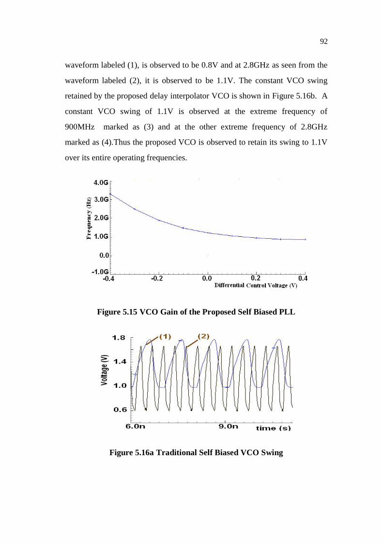
92
waveform labeled (1), is observed to be 0.8V and at 2.8GHz as seen from the
waveform labeled (2), it is observed to be 1.1V. The constant VCO swing
retained by the proposed delay interpolator VCO is shown in Figure 5.16b. A
constant VCO swing of 1.1V is observed at the extreme frequency of
900MHz marked as (3) and at the other extreme frequency of 2.8GHz
marked as (4).Thus the proposed VCO is observed to retain its swing to 1.1V
over its entire operating frequencies.
Figure 5.15 VCO Gain of the Proposed Self Biased PLL
Figure 5.16a Traditional Self Biased VCO Swing

93
Figure 5.16b Proposed Self Biased VCO Swing
The bias voltage transients of the traditional and proposed self
biased PLL are shown in Figure 5.17 at an operating frequency of 2.1GHz.
From the bias voltage transients Vbn of the traditional self biased PLL and Vbn-
_slow and Vbn_fast of the proposed PLL, it can be observed that both the system
settles very closer. The traditional self biased PLL is observed to settle at
110ns (14 reference clock cycles) and the settling time of the proposed self
biased PLL is found to be very closer at 114ns (15reference clock cycles)
with a frequency step of 700MHz.
Figure 5.17 Capture Transients of Bias Voltages of the Traditional and the Proposed Self Biased PLL at 2.1GHz

94
The peak to peak jitter measure using an eye diagram plot is shown
in Figure 5.18 for the two architectures at the operating frequencies of
2.1GHz. The peak to peak jitter measure for the traditional self biased PLL
architecture is 12.4ps where as for the proposed self biased PLL it is observed
to be 5.9ps, thereby the proposed PLL shows 52% improvement in jitter
performance.
The proposed PLL operates over wide frequency range of 1GHz to
2.1GHz. The PLL performance at these extreme frequencies of 1GHz and
2.1GHz are tabulated in Table 5.2. From the table it can be noted that
significant jitter performance improvement of 47% to 85% is obtained
without any degradation in its settling time. The settling time is measured for
a frequency step of 400MHz.
Supply rejection characteristic is verified by simulating supply
noise as a sinusoidal source of 10mV with 100MHz frequency added with the
Figure 5.18 Jitter Performance at 2.1GHz output frequency

95
Table 5.2 Performance comparison at extreme operating frequencies
Performance
parameter
Output
frequency
(MHz)
Traditional
self biased
PLL
Proposed
self biased
PLL
Jitter (ps)
(UI%)
1000
3.8
(0.38)
0.6
(0.06)
Settling time ( s)
(reference clock
cycles)
0.210
(13)
0.216
(14)
RMS Jitter (ps)
(UI %)
2720 1.6
(0.43)
0.8
(0.21)
Settling time ( s)
(reference clock
cycles)
0.160
(27)
0.188
(32)
Capture range
(MHz)
1000-2700 900-2700
DC supply source. The observed jitter for the traditional PLL under this noisy
supply is 38.6ps and for the proposed PLL the jitter is observed to be 13.8ps
showing 64% improvement. There is a marginal degradation while comparing
jitter performance improvement with the noiseless case of 1GHz output
frequency, as the bias generator of the proposed PLL drives a larger
capacitive load, hence the gain at 100MHz supply noise of the proposed PLL
bias generator degrades when compared with the gain of the traditional self
biased PLL bias generator.

96
5.3 SUMMARY
The present chapter thus described a feasible circuit realization of
the third order self biased adaptive bandwidth PLL. It was shown that the
system is stable for a wide capture range. It was also demonstrated that the
third order PLL provides improvement in performance with respect to (a)
jitter (b) settling time (c) undershoot/overshoot transients. Even though the
circuit was not designed optimally for power, the third order system exhibits
this performance improvement over the second order system only on a
marginal increase of 10% in its power consumption.
Following the third order PLL, this chapter also shows the
possiblity to suitably combine the traditional self biased PLL and the delay
interpolator VCO in order to derive the benefits of both the schemes. The
modified PLL showed significant improvement in jitter in comparison to the
traditional self biased PLL without exhibiting any degradation in the settling
time. Since the system bandwidth is adaptive, the proposed PLL exhibited
wide capture range spanning of 1.7GHz. It was also observed that the
proposed scheme is capable of jitter improvements ranging from 46% to 85 %
with marginal degradation in the capture time and supply rejection
characteristics. It was also shown that the VCO swing in the proposed PLL
has a constant signal swing of 1.1V over the entire operating frequency range.