chapter 3 - top level view of computer function
TRANSCRIPT

Chapter 3 - Top Level View of Computer Function
Luis Tarrataca
CEFET-RJ
L. Tarrataca Chapter 3 - Top Level View 1 / 127

Table of Contents I
1 Introduction
2 Computer Components
3 Computer Function
Basic instruction cycle
A more detailed instruction cycle
4 Interrupts
5 Multiple Interrupts
6 Multiple Interrupts
7 Bus Interconnection
Bus Structure
Data Lines
Address Lines
L. Tarrataca Chapter 3 - Top Level View 2 / 127

Table of Contents IIControl Lines
Multiple-Bus Hierarchies
Elements of bus design
Bus Type
Timing
8 References
L. Tarrataca Chapter 3 - Top Level View 3 / 127

Introduction
Introduction
• Today we will focus on presenting a top-level view of computer function.
• We will be interested in answering the following questions:
What are the main components of computer function?
L. Tarrataca Chapter 3 - Top Level View 4 / 127
Introduction
Introduction
• Today we will focus on presenting a top-level view of computer function.
• We will be interested in answering the following questions:
How are these components organized?
L. Tarrataca Chapter 3 - Top Level View 5 / 127

Introduction
Introduction
• Today we will focus on presenting a top-level view of computer function.
• We will be interested in answering the following questions:
How do these components communicate with each other?
L. Tarrataca Chapter 3 - Top Level View 6 / 127

Introduction
Anyone has any idea how to answer the previous questions?
• What are the main components of computer function?
• How are these components organized?
• How do these components communicate with each other?
Any ideas?
L. Tarrataca Chapter 3 - Top Level View 7 / 127

Introduction
At a top level, a computer consists of:
• Central Processing Unit;
• Memory;
• I/O components.
The components are interconnected in order to execute programs.
L. Tarrataca Chapter 3 - Top Level View 8 / 127

Introduction
This interconnection requires:
• control signals to:
• control other components;
• be controlled by other components;
• data signals to:
• exchange information with other components.
• an infrastructure to send / receive all these signals.
Lets have a top down look into some of these components...
L. Tarrataca Chapter 3 - Top Level View 9 / 127

Computer Components
Computer Components
Most computer concepts were developed by this person:
Does anyone know who this person is?
• 1 extra point if you answer in 10 seconds... #NOT
L. Tarrataca Chapter 3 - Top Level View 10 / 127

Computer Components
Computer Components
Most computer concepts were developed by John von Neumann:
• Hungarian-born scientist;
• Worked on the Manhattan Project;
• Prolific contributor to diverse fields:
• Physics;
• Mathematics;
• Economics;
• Game theory;
• ...
• One of humanity’s greatest minds.
L. Tarrataca Chapter 3 - Top Level View 11 / 127

Computer Components
Von Neumann architecture is based on three concepts:
• Ability to write/read data from memory;
• Ability to execute instruction sequentially;
• Ability to process inputs/outputs;
L. Tarrataca Chapter 3 - Top Level View 12 / 127

Computer Components
Von Neumann architecture is based on three concepts:
• Ability to write/read data from memory;
• Ability to execute instruction sequentially;
• Ability to process inputs/outputs;
But why we need these components? Any ideas?
L. Tarrataca Chapter 3 - Top Level View 13 / 127

Computer Components
Consider the original method for computation based on digital circuits:
• Allow us to calculate binary functions.
• Employs a small set of logical gates:
• AND, OR, NOT, NAND, NOR, XOR, XNOR
• Employ some type of memory:
• Flip-flop SR, JK, D
L. Tarrataca Chapter 3 - Top Level View 14 / 127

Computer Components
Do you see any disadvantage with using digital circuits? Any ideas?
L. Tarrataca Chapter 3 - Top Level View 15 / 127
Computer Components
Do you see any disadvantage with using digital circuits? Any ideas?
• Rigid design:
• Only works for a specific function...
• What if we need to calculate additional functions?
• Requires generating a new circuit...
• producing new truth tables;
• algebraic simplification;
• circuit design.
• Basically a lot of work...
L. Tarrataca Chapter 3 - Top Level View 16 / 127

Computer Components
So what can be done to circumvent this problem? Any ideas?
L. Tarrataca Chapter 3 - Top Level View 17 / 127

Computer Components
Suppose that instead of having such an hardwired circuit we have:
• A module capable of calculating arithmetic/logic functions:
• Logic functions:
• AND, OR, NOT, NAND, NOR, XOR, XNOR
• Arithmetic functions:
• addition, subtraction, multiplication, division, SHL, SHR,...
L. Tarrataca Chapter 3 - Top Level View 18 / 127

Computer Components
• We need also need a way to control such a module:
• control signals indicate which operation to do;
• data forwarding mechanisms:
• to provide input to the arithmetic / logic functions;
• to store the output of such functions.
L. Tarrataca Chapter 3 - Top Level View 19 / 127
Computer Components
• With such a general-purpose hardware:
• System accepts data and control signals and produces results.
• Programmer merely needs to supply a new set of control signals.
• instead of rewiring the hardware for each new program;
L. Tarrataca Chapter 3 - Top Level View 20 / 127

Computer Components
Regarding the control signals...
How shall the control signals be supplied? Any ideas?
L. Tarrataca Chapter 3 - Top Level View 21 / 127

Computer Components
How shall the control signals be supplied?
• Program is a sequence of steps;
• At each step, an arithmetic/logical operation is performed on data;
• Each instruction thus requires its own set of control signals =)
• Hardware interprets each instruction and generates control signals.
L. Tarrataca Chapter 3 - Top Level View 22 / 127

Computer Components
The Central Processing Unit (CPU) incorporates these two responsibilities:
• An instruction interpreter capable of generating control signals;
• A general-purpose module for arithmetic/logic functions.
L. Tarrataca Chapter 3 - Top Level View 23 / 127

Computer Components
• CPU provides a way to perform arithmetic/logic operations;
Is this capability enough to have a functional computer? Any ideas?
L. Tarrataca Chapter 3 - Top Level View 24 / 127

Computer Components
• CPU provides a way to perform arithmetic/logic operations;
Is this capability enough to have a functional computer? Any ideas?
• Several other components are needed to yield a functioning computer.
L. Tarrataca Chapter 3 - Top Level View 25 / 127

Computer Components
Data and instructions must be provided to the system:
• Input module:
• contains basic components for accepting data and instructions
• Output module:
• contains the means of reporting results.
Taken together, these are referred to as I/O components.
Are these two components enough for a functional computer? Any
ideas?
L. Tarrataca Chapter 3 - Top Level View 26 / 127

Computer Components
Data operations may require access to more than one element:
• there must be a place to store both instructions and data.
• that module is called main memory
• to distinguish it from external storage or peripheral devices.
L. Tarrataca Chapter 3 - Top Level View 27 / 127

Computer Components
Von Neumman architecture
We have thus the main components of the von Neumann architecture:
• Memory module
• I/O module
• CPU
L. Tarrataca Chapter 3 - Top Level View 28 / 127

Computer Components
Guess what we will be doing next? Any ideas?
L. Tarrataca Chapter 3 - Top Level View 29 / 127

Computer Components
Guess what we will be doing next? Any ideas?
• We will be having a more detailed look at these components...
L. Tarrataca Chapter 3 - Top Level View 30 / 127

Computer Components
Figure: A top level view of the main computer components (Source: [Stallings, 2015])
L. Tarrataca Chapter 3 - Top Level View 31 / 127

Computer Components
CPU has a set of internal registers (1/3):
• Program Counter (PC):
• specifies the memory address of the next instruction to be executed.
• Instruction Register (IR):
• holds the instruction currently being executed or decoded.
L. Tarrataca Chapter 3 - Top Level View 32 / 127

Computer Components
CPU has a set of internal registers (2/3):
• memory address register (MAR):
• specifies memory address to be read/written;
• memory buffer register (MBR):
• contains the data to be written into memory or...
• receives the data read from memory;
L. Tarrataca Chapter 3 - Top Level View 33 / 127

Computer Components
CPU has a set of internal registers (3/3):
• I/O address register (I/OAR):
• specifies a particular I/O device;
• I/O buffer (I/OBR) register:
• used for the exchange of data between an I/O module and the CPU;
L. Tarrataca Chapter 3 - Top Level View 34 / 127

Computer Components
Memory module consists of:
• a set of sequentially numbered addresses:
• Each location contains binary information
• data;
• or instructions.
L. Tarrataca Chapter 3 - Top Level View 35 / 127

Computer Components
I/O module responsible for:
• transfers data from external devices to CPU and memory;
• and vice versa
• containing internal buffers for temporarily holding data
L. Tarrataca Chapter 3 - Top Level View 36 / 127

Computer Function
Computer Function
Basic function performed by a computer is execution of a program:
• consisting of a set of instructions stored in memory;
• processor does the actual work by executing the specified instructions;
This gives us a hint of how to perform instruction processing...
L. Tarrataca Chapter 3 - Top Level View 37 / 127

Computer Function Basic instruction cycle
Basic instruction cycle
In its simplest form, instruction processing consists of two steps:
• Fetch stage:
• processor reads instructions from memory one at a time
• Execution stage:
• processor executes the instruction
Figure: Basic Instruction Cycle (Source: [Stallings, 2015])
L. Tarrataca Chapter 3 - Top Level View 38 / 127

Computer Function Basic instruction cycle
Figure: Basic Instruction Cycle (Source: [Stallings, 2015])
Program execution consists of a loop:
1 fetch instruction stage;
2 execute instruction stage;
L. Tarrataca Chapter 3 - Top Level View 39 / 127

Computer Function Basic instruction cycle
At the beginning of each instruction cycle:
• Processor fetches an instruction from memory;
• Program counter holds the address of the instruction to be fetched;
• After each instruction fetch the PC is incremented. Why?
• so that it will fetch the next instruction;
• i.e., the instruction located at the next memory address;
• recall that memory is organized into sequential units of storage;
L. Tarrataca Chapter 3 - Top Level View 40 / 127

Computer Function Basic instruction cycle
Example
Consider a computer where each instruction occupies 16-bits in memory.
• Assume that the PC is set to memory location 300;
• Each location address contains a 16-bit word;
• The processor will next fetch the instruction at location 300.
• On succeeding instruction cycles, it will fetch instructions from locations:
1 301;
2 302;
3 and so on.
• This sequence may be altered. Why?
• Conditional jumps (IF’s) to other areas of code.
L. Tarrataca Chapter 3 - Top Level View 41 / 127

Computer Function Basic instruction cycle
The fetched instruction is loaded into a register in the processor
• known as the instruction register (IR);
• the instruction specifies control signals for the processor;
• the processor interprets the instruction and performs the required action.
L. Tarrataca Chapter 3 - Top Level View 42 / 127

Computer Function Basic instruction cycle
What types of actions are usually performed?
In general, these actions fall into four categories:
• Processor ↔ memory data transfers;
• Processor ↔ I/O peripherals data transfers;
• Data processing: arithmetic or logic operations on data;
• Control: E.g. alter the PC because of conditional jumps (IF’s)
L. Tarrataca Chapter 3 - Top Level View 43 / 127

Computer Function Basic instruction cycle
Seems confusing? Well, maybe it helps if we use an example... =)
L. Tarrataca Chapter 3 - Top Level View 44 / 127
Computer Function Basic instruction cycle
Example ( 1 / 11 )
Consider a processor:
• containing a single data register, called an accumulator (AC).
• both instructions and data are 16 bits long;
• thus, it is convenient to organize memory using 16-bit words;
L. Tarrataca Chapter 3 - Top Level View 45 / 127

Computer Function Basic instruction cycle
Example ( 2 / 11 )
• The instruction format is the following:
Figure: Instruction Format (Source: [Stallings, 2015])
• Opcode: code of the operation to be executed (+,-,×, ÷,etc...);
• How many bits are reserved for the opcode? Total combinations?
• Addressing memory,
• How many bits are reserved for the addressing memory? Total combinations?
L. Tarrataca Chapter 3 - Top Level View 46 / 127

Computer Function Basic instruction cycle
Example ( 2 / 11 )
• The instruction format is the following:
Figure: Instruction Format (Source: [Stallings, 2015])
• Opcode: code of the operation to be executed (+,-,×, ÷,etc...);
• 4 bits are reserved, i.e there can be 24
different opcodes;
• Addressing memory,
• 12 bits are reserved, i.e. 212
memory words can be addressed.
L. Tarrataca Chapter 3 - Top Level View 47 / 127

Computer Function Basic instruction cycle
Example ( 3 / 11 )
Consider that we have the following opcodes:
0001 Load AC from memory
0010 Store AC to memory
0101 Add to AC from memory
Also, each number requires 16 bits and has the following representation:
Figure: Integer Format
• One bit for signal;
• 15-bits for magnitude.
L. Tarrataca Chapter 3 - Top Level View 48 / 127

Computer Function Basic instruction cycle
Example ( 4 / 11 )
Now lets try to execute the following instructions (assume PC=300):
1 Add memory contents at address 940 to the contents at address 941;
2 store the result in the latter location.
Any ideas of how all the previous concepts will function and interconnect
with each other?
L. Tarrataca Chapter 3 - Top Level View 49 / 127

Computer Function Basic instruction cycle
Example ( 5 / 11 )
Assume PC=300:
Figure: Example of Program Execution (contents
of memory and registers in hexadecimal)
(Source: [Stallings, 2015])
Opcodes:
0001 Load AC from memory
0010 Store AC to memory
0101 Add to AC from memory
L. Tarrataca Chapter 3 - Top Level View 50 / 127

Computer Function Basic instruction cycle
Example ( 6 / 11 )
Assume PC=300:
Figure: Example of Program Execution (contents
of memory and registers in hexadecimal)
(Source: [Stallings, 2015])
Opcodes:
0001 Load AC from memory
0010 Store AC to memory
0101 Add to AC from memory
L. Tarrataca Chapter 3 - Top Level View 51 / 127

Computer Function Basic instruction cycle
Example ( 7 / 11 )
Assume PC=300:
Figure: Example of Program Execution (contents
of memory and registers in hexadecimal)
(Source: [Stallings, 2015])
Opcodes:
0001 Load AC from memory
0010 Store AC to memory
0101 Add to AC from memory
L. Tarrataca Chapter 3 - Top Level View 52 / 127

Computer Function Basic instruction cycle
Example ( 8 / 11 )
Assume PC=300:
Figure: Example of Program Execution (contents
of memory and registers in hexadecimal)
(Source: [Stallings, 2015])
Opcodes:
0001 Load AC from memory
0010 Store AC to memory
0101 Add to AC from memory
L. Tarrataca Chapter 3 - Top Level View 53 / 127

Computer Function Basic instruction cycle
Example ( 9 / 11 )
Assume PC=300:
Figure: Example of Program Execution (contents
of memory and registers in hexadecimal)
(Source: [Stallings, 2015])
Opcodes:
0001 Load AC from memory
0010 Store AC to memory
0101 Add to AC from memory
L. Tarrataca Chapter 3 - Top Level View 54 / 127

Computer Function Basic instruction cycle
Example ( 10 / 11 )
Assume PC=300:
Figure: Example of Program Execution (contents
of memory and registers in hexadecimal)
(Source: [Stallings, 2015])
Opcodes:
0001 Load AC from memory
0010 Store AC to memory
0101 Add to AC from memory
L. Tarrataca Chapter 3 - Top Level View 55 / 127

Computer Function Basic instruction cycle
Example ( 11 / 11 )
In textual form:
1 The PC contains value 300, the address of the first instruction.
1 This instruction (the value 1940 in hexadecimal) is loaded into the instruction register
IR, and the PC is incremented;
2 The first 4 bits (first hexadecimal digit) in the IR indicate that the AC is to be loaded.
1 The remaining 12 bits (three hexadecimal digits) specify the address (940) from
which data are to be loaded.
3 The next instruction (5941) is fetched from location 301, and the PC is incremented.
4 The old contents of the AC and the contents of location 941 are added, and the result is
stored in the AC.
5 The next instruction (2941) is fetched from location 302, and the PC is incremented.
6 The contents of the AC are stored in location 941.
L. Tarrataca Chapter 3 - Top Level View 56 / 127

Computer Function Basic instruction cycle
Some important notes:
• the last example was very simplified;
• but the overall control structure and information flow is present;
• However, there are a lot of details missing;
Lets look into a more detailed instruction cycle...
L. Tarrataca Chapter 3 - Top Level View 57 / 127

Computer Function A more detailed instruction cycle
A more detailed look at the basic instruction cycle:
Figure: A more realistic instruction cycle state diagram (Source: [Stallings, 2015])
L. Tarrataca Chapter 3 - Top Level View 58 / 127

Computer Function A more detailed instruction cycle
The states can be described as follows (1/2):
• Instruction address calculation (IAC):
• Determine address of next instruction to be executed;
• Instruction fetch (IF):
• Read instruction from memory into the processor;
• Instruction operation decoding (IOD):
• Determine type of operation to be performed and operand(s) to be used.
L. Tarrataca Chapter 3 - Top Level View 59 / 127

Computer Function A more detailed instruction cycle
The states can be described as follows (2/2):
• Operand address calculation (OAC):
• Determine the address of the operand.
• Operand fetch (OF):
• Fetch the operand from memory or read it in from I/O.
• Data operation (DO):
• Perform the operation indicated in the instruction.
• Operand store (OS):
• Write the result into memory or to I/O.
L. Tarrataca Chapter 3 - Top Level View 60 / 127

Computer Function A more detailed instruction cycle
Now that we have seen this more detailed instruction cycle...
Do you think it is enough? Should we add other states? Is there something
missing?
L. Tarrataca Chapter 3 - Top Level View 61 / 127

Computer Function A more detailed instruction cycle
Now that we have seen this more detailed instruction cycle...
Do you think it is enough? Should we add other states? Is there something
missing?
• What if an error occurs?
• What if we want to execute something periodically?
• What if we want to read data from an input device (e.g.: keyboard)?
• etc....
L. Tarrataca Chapter 3 - Top Level View 62 / 127

Interrupts
Interrupts
There exists some situations where we may want to interrupt the CPU:
• Program: arithmetic overflow, division by zero, segfault, etc..
• Timer: execute something periodically;
• I/O: exchange communication between I/O devices and the processor;
• Hardware: generated by an hardware failure
• e.g.: power, memory parity error, etc;
L. Tarrataca Chapter 3 - Top Level View 63 / 127

Interrupts
Because of these reasons (and some others):
• Computers provide a mechanism to interrupt the processing;
• Any ideas of the mechanism name?
L. Tarrataca Chapter 3 - Top Level View 64 / 127

Interrupts
Because of these reasons (and some others):
• Virtually all computers provide a mechanism to interrupt the normal
processing of the processor.
• Any ideas of the mechanism name?
• Interruptions =)
L. Tarrataca Chapter 3 - Top Level View 65 / 127

Interrupts
Can you see any implications for interrupting the processor?
L. Tarrataca Chapter 3 - Top Level View 66 / 127

Interrupts
Can you see any implications for interrupting the processor?
1 An interrupt request signal is sent to the processor.
2 The processor responds by suspending current program execution;
• What does this imply? Any ideas? (See Slide 73)
3 The processor executes a routine capable of dealing with the interrupt;
• A.k.a. interruption handler.
4 After the handler finishes the program returns to the original execution.
• What does this imply? Any ideas? (See Slide 74)
L. Tarrataca Chapter 3 - Top Level View 67 / 127

Interrupts
Figure: Transfer of control via interrupts (Source: [Stallings, 2015])
L. Tarrataca Chapter 3 - Top Level View 68 / 127

Interrupts
So, the question now is how can the processor detect interruptions?
Any ideas?
L. Tarrataca Chapter 3 - Top Level View 69 / 127

Interrupts
Lets quickly remember the basic instruction cycle:
Figure: A more realistic instruction cycle state diagram (Source: [Stallings, 2015])
L. Tarrataca Chapter 3 - Top Level View 70 / 127

Interrupts
Lets quickly remember the basic instruction cycle:
Figure: A more realistic instruction cycle state diagram (Source: [Stallings, 2015])
To accommodate interrupts:
• An interrupt cycle can be added to the end of instruction cycle...
L. Tarrataca Chapter 3 - Top Level View 71 / 127

Interrupts
To add interrupts, an interrupt cycle can be added...
Figure: Instruction Cycle State Diagram, with Interrupts (Source: [Stallings, 2015])
HINT: This is one of the most important slides of the entire semester ;)
L. Tarrataca Chapter 3 - Top Level View 72 / 127

Interrupts
Interruption Processing (1/4)
• Processor checks to see if any interrupts have occurred
• indicated by the presence of an interrupt signal;
• If no interrupts are pending:
1 processor proceeds to the fetch cycle and...
2 fetches the next instruction of the current program.
L. Tarrataca Chapter 3 - Top Level View 73 / 127

Interrupts
Interruption Processing (2/4)
• If an interrupt is pending, the processor does the following (1/3):
1 suspends execution of the program being executed. This entails:
• Saving the PC;
• Saving the contents of the registers;
• This is called saving the context of the program
2 sets the PC to the starting address of an interrupt handler routine;
L. Tarrataca Chapter 3 - Top Level View 74 / 127
Interrupts
Interruption Processing (3/4)
• If an interrupt is pending, the processor does the following (2/3):
3 The instruction cycle is restarted, but this time for the interruption handler;
• fetch the first instruction in the interrupt handler program
• etc...
• Eventually the interruption routine will terminate;
L. Tarrataca Chapter 3 - Top Level View 75 / 127

Interrupts
Interruption Processing (4/4)
• If an interrupt is pending, the processor does the following (3/3):
4 When the interrupt handler routine is completed:
• Processor needs to resume execution of the original program;
• Processor restores contents of the previously saved registers...
• ...Continuing the execution of the previously saved PC;
• This is called restoring the context of the program
L. Tarrataca Chapter 3 - Top Level View 76 / 127

Interrupts
Can you see any problem with the interruption scheme?
L. Tarrataca Chapter 3 - Top Level View 77 / 127

Interrupts
Can you see any problem with the interruption scheme?
There is some overhead involved in this process:
• Extra instructions must be executed:
• to determine the nature of the interrupt;
• decide the appropriate action.
• However:
• Not enough to offset the performance of waiting on, e.g., I/O operations.
L. Tarrataca Chapter 3 - Top Level View 78 / 127
Interrupts
We now have a basic understanding of the interruption mechanism...
But what if multiple interruptions being generated at the same time?
Example:
• A key is pressed;
• A segfault is generated;
L. Tarrataca Chapter 3 - Top Level View 79 / 127

Multiple Interrupts
Multiple Interrupts
Suppose that multiple interrupts can occur, e.g.: a program may be
• receiving data from a communications line:
• an interruption is generated every time a unit of data arrives.
• printing:
• an interruption is generated every time a print operation is completed;
How should the system deal with such cases? Any ideas?
L. Tarrataca Chapter 3 - Top Level View 80 / 127

Multiple Interrupts
Multiple Interrupts
Suppose that multiple interrupts can occur, e.g.: a program may be
• receiving data from a communications line:
• an interruption is generated every time a unit of data arrives.
• printing:
• an interruption is generated every time a print operation is completed;
How should the system deal with such cases? Any ideas?
• The are two possibilities...
L. Tarrataca Chapter 3 - Top Level View 81 / 127

Multiple Interrupts
What can we do to solve this issue? Any ideas?
L. Tarrataca Chapter 3 - Top Level View 82 / 127

Multiple Interrupts
1st Possibility
Disable interrupts while an interrupt is being processed:
• The processor will ignore interrupt request signals;
• Emphasis on the ‘‘ignore’’, interrupt signals can still be generated.
• After the interrupt handler routine completes:
• Interrupts are enabled;
• the processor checks to see if any interrupts have occurred.
L. Tarrataca Chapter 3 - Top Level View 83 / 127
Multiple Interrupts
Can you see any problem with this approach of disabling interrupts while
processing an interruption?
L. Tarrataca Chapter 3 - Top Level View 84 / 127
Multiple Interrupts
Can you see any problem with this approach of disabling interrupts while
processing an interruption?
• Some interruptions may be more important than others.
• Some important examples...
• Nuclear reactor;
• Plane steering;
• Ventilator system.
L. Tarrataca Chapter 3 - Top Level View 85 / 127

Multiple Interrupts
2nd Possibility
Allow each interruption to have a priority:
• Higher priority interruptions can interrupt lower-priority interruptions.
• This strategy is referred to as nested interrupt processing.
L. Tarrataca Chapter 3 - Top Level View 86 / 127

Multiple Interrupts
Example (1/3)
Consider a system with three I/O devices:
Device Interruption Priority
Printer 2
Disk 4
Comm. line 5
Figure: Example Time Sequence of Multiple Interrupts (Source: [Stallings, 2015])L. Tarrataca Chapter 3 - Top Level View 87 / 127

Multiple Interrupts
Example (2/3)
Program begins at t = 0 and at t = 10, a printer interrupt occurs:
1 context is saved;
2 execution goes to the printer interrupt service routine (ISR);
3 While this routine is executing (t = 15), a communications interrupt occurs:
1 Higher priority than the printer;
2 Printer ISR is interrupted, context is saved;
3 Execution goes to the communication ISR;
1 While this routine is executing, a disk interrupt occurs (t = 20);
2 Because this interrupt is of lower priority, it is simply held;
3 and the communications ISR runs to completion.
L. Tarrataca Chapter 3 - Top Level View 88 / 127

Multiple Interrupts
Example (3/3)
4 When the communications ISR completes (t = 25):
1 printer ISR state is restored;
2 However, there is a pending higher-priority interruption (disk);
1 Processor transfers control to the disk ISR;
2 disk ISR completes at t = 35;
3 printer ISR is resumed;
4 printer ISR terminates at t = 40;
5 control returns to the original program.
L. Tarrataca Chapter 3 - Top Level View 89 / 127

Multiple Interrupts
Now that we have seen the interruptions scheme lets transition to a different
topic =)
L. Tarrataca Chapter 3 - Top Level View 90 / 127

Bus Interconnection
Interconnection Issues
A computer consists of a set basic types of components:
These modules need to communicate with each other in order to :
• exchange data;
• exchange control signals;
• ...
L. Tarrataca Chapter 3 - Top Level View 91 / 127

Bus Interconnection
Any idea how this communication can be performed?
L. Tarrataca Chapter 3 - Top Level View 92 / 127

Bus Interconnection
Any idea how this communication can be performed?
• Through a bus...
L. Tarrataca Chapter 3 - Top Level View 93 / 127

Bus Interconnection
Any idea how this communication can be performed?
• Through a bus...
Ok, so what is a ‘‘bus’’? Any ideas?
L. Tarrataca Chapter 3 - Top Level View 94 / 127

Bus Interconnection
Bus Interconnection
A bus is a communication pathway connecting two or more devices:
• shared transmission medium;
• connected devices can pickup the reception of all other devices.
• If several devices transmit during the same time period:
• their signals will overlap and become garbled:
• thus, only one device at a time can successfully transmit.
L. Tarrataca Chapter 3 - Top Level View 95 / 127

Bus Interconnection
A bus consists of multiple communication lines:
• Each line transmits binary signals.
• A sequence of binary digits can be transmitted:
• using a single line over time (i.e. sequentially);
• several lines can be used (i.e. in parallel ).
A bus connecting major computer components is called a system bus.
L. Tarrataca Chapter 3 - Top Level View 96 / 127

Bus Interconnection
Now that we know the basic function of the bus...
What type of information does the bus carry? Any ideas?
L. Tarrataca Chapter 3 - Top Level View 97 / 127

Bus Interconnection Bus Structure
Bus Structure
Bus lines can be classified into three functional groups:
• data:
• for moving data among system modules
• address
• for specifying the source or destination of the data:
• control
• for transmiting command information among the modules.
Lets have a quick look into each one of these...
L. Tarrataca Chapter 3 - Top Level View 98 / 127

Bus Interconnection Bus Structure
Figure: Bus Interconnection Scheme (Source: [Stallings, 2015])
L. Tarrataca Chapter 3 - Top Level View 99 / 127
Bus Interconnection Bus Structure
Data Lines
The data bus may consist of 32, 64, 128, or even more separate lines:
• a.k.a. width of the data bus;
Each line can carry only 1 bit at a time:
• the number of lines determines how many bits can be transferred at a time.
Data bus width is key to system performance, e.g.:
• if the data bus is 32 bits wide and each instruction is 64 bits long;
• Each instruction requires two memory acesses.
L. Tarrataca Chapter 3 - Top Level View 100 / 127

Bus Interconnection Bus Structure
Address Lines
Used to designate the source or destination of the data on the data bus:
• The width of the address bus determines the maximum system memory;
• The address lines are generally also used to address I/O addresses;
• Higher-order bits are used to select a particular module on the bus;
• Lower-order bits select a memory location or I/O port within the module.
L. Tarrataca Chapter 3 - Top Level View 101 / 127

Bus Interconnection Bus Structure
Control Lines
Command signals specify operations to be performed, e.g.:
• Memory write: write bus data to a memory address;
• Memory read: read memory at memory address;
• I/O write: write bus data to an I/O address;
• I/O read: read data from an I/O address;
• Bus request: a module needs to gain control of the bus;
• Bus grant: a requesting module has been granted bus control;
• Many more control signals...
L. Tarrataca Chapter 3 - Top Level View 102 / 127

Bus Interconnection Bus Structure
Ok, now that we know a little bit more about bus function:
Can you see any potential problem with bus usage?
L. Tarrataca Chapter 3 - Top Level View 103 / 127

Bus Interconnection Bus Structure
Ok, now that we know a little bit more about bus function:
Can you see any potential problem with bus usage?
L. Tarrataca Chapter 3 - Top Level View 104 / 127

Bus Interconnection Bus Structure
Ok, now that we know a little bit more about bus function:
Can you see any potential problem with bus usage?
What happens if a great number of devices are connected to the bus?
L. Tarrataca Chapter 3 - Top Level View 105 / 127
Bus Interconnection Bus Structure
Ok, now that we know a little bit more about bus function:
Can you see any potential problem with bus usage?
What happens if a great number of devices are connected to the bus?
• If a great number of devices are connected bus performance will suffer.
L. Tarrataca Chapter 3 - Top Level View 106 / 127

Bus Interconnection Multiple-Bus Hierarchies
Multiple-Bus Hierarchies
Main variables of bus performance (1/2):
• Bus length: the more devices attached to the bus, the greater the bus
length and hence the greater the propagation delay.
• Delay determines time required for devices to coordinate bus use;
• When bus control is passed frequently between device:
• propagation delay can noticeably affect performance.
L. Tarrataca Chapter 3 - Top Level View 107 / 127
Bus Interconnection Multiple-Bus Hierarchies
Main variables of bus performance (2/2):
• Bus capacity: bus has a certain data rate capacity:
• aggregate data transfer bottleneck;
• possible solutions:
• increase data rate;
• use wider bus;
L. Tarrataca Chapter 3 - Top Level View 108 / 127

Bus Interconnection Multiple-Bus Hierarchies
So, what is the overall solution to this problem? Any ideas?
L. Tarrataca Chapter 3 - Top Level View 109 / 127
Bus Interconnection Multiple-Bus Hierarchies
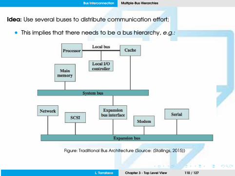
Idea: Use several buses to distribute communication effort;
• This implies that there needs to be a bus hierarchy, e.g.:
Figure: Traditional Bus Architecture (Source: [Stallings, 2015])
L. Tarrataca Chapter 3 - Top Level View 110 / 127

Bus Interconnection Multiple-Bus Hierarchies
• Local bus connecting:
• processor;
• cache memory;
• one or more local
devices.
• System bus:
• where the main memory
module is attached;
• that also connects to the
cache;
Note: in contemporary systems, the
cache is in the same chip as the pro-
cessor.
Figure: Traditional Bus Architecture (Source: [Stallings, 2015])
L. Tarrataca Chapter 3 - Top Level View 111 / 127

Bus Interconnection Elements of bus design
Elements of bus design
Parameters that can be used to classify and differentiate buses e.g.:
Figure: Elements of bus design (Source: [Stallings, 2015])
Lets have a look at some of these...
L. Tarrataca Chapter 3 - Top Level View 112 / 127

Bus Interconnection Elements of bus design
Bus Type
Bus lines can be separated into two generic types:
• dedicated: line is used for a single purpose:
• e.g.: the use of separate dedicated address and data lines
• multiplexed: line is used for multiple purposes:
• e.g.: address and data information may be transmitted over the same lines
• Idea: use an Address Valid control line:
• Activate Address Valid line;
• Place the address on the bus lines;
• Transfer the data after.
L. Tarrataca Chapter 3 - Top Level View 113 / 127

Bus Interconnection Elements of bus design
Can you see any advantages / disadvantages with multiplexing?
L. Tarrataca Chapter 3 - Top Level View 114 / 127

Bus Interconnection Elements of bus design
Multiplexing advantage:
• use of fewer lines, which saves space and, usually, cost.
Multiplexing disadvantage:
• more complex circuitry is needed within each module;
• potential reduction in performance:
• certain events that share the same lines cannot take place in parallel.
L. Tarrataca Chapter 3 - Top Level View 115 / 127

Bus Interconnection Elements of bus design
Timing
Refers to the way in which events are coordinated on the bus:
• synchronous timing: occurrence of events is determined by a clock.
• bus includes a clock line, connected to a system clock;
• A single 1-0 transmission is referred to as a clock cycle;
• Devices on the bus can read the clock line;
• all events start at the beginning of a clock cycle:
L. Tarrataca Chapter 3 - Top Level View 116 / 127

Bus Interconnection Elements of bus design
Synchronous Example (1/3)
Figure: Timing of Synchronous Bus Operations (Source: [Stallings, 2015])
L. Tarrataca Chapter 3 - Top Level View 117 / 127

Bus Interconnection Elements of bus design
Synchronous Example (2/3)
1 Processor sets various status lines;
2 Processor places a memory address on the address lines;
3 Once the address lines have stabilized, the processor issues an address enable signal;
L. Tarrataca Chapter 3 - Top Level View 118 / 127

Bus Interconnection Elements of bus design
Synchronous Example (3/3)
4 The example then depicts two operations:
• read cycle:
• Processor issues a read command (start of the second cycle);
• Memory module recognizes address and, after a delay of one cycle, places
the data on the data lines;
• Processor reads the data from the data lines and drops the read signal;
• write cycle:
• Processor puts the data on the data lines (start of the second cycle);
• Processor issues a write command after the data lines have stabilized;
• Memory module copies the information from the data lines (third clock cycle).
L. Tarrataca Chapter 3 - Top Level View 119 / 127

Bus Interconnection Elements of bus design
Asynchronous Example (1/5)
Asynchronous timing: occurrence of one bus event follows and depends on
the occurrence of a previous event.
E.g.: read operation using an asynchronous bus:
Figure: System bus read cycle (Source: [Stallings, 2015])
L. Tarrataca Chapter 3 - Top Level View 120 / 127

Bus Interconnection Elements of bus design
Asynchronous Example (2/5)
1 Processor places address and status signals on bus;
2 After pausing for these signals to stabilize, it issues a read command;
• indicating the presence of valid address and control signals.
3 Memory performs the following tasks:
1 decodes the address
2 places the data on the data line;
4 Once the data lines have stabilized:
1 memory module asserts the acknowledged line to signal the processor that
the data are available.
L. Tarrataca Chapter 3 - Top Level View 121 / 127

Bus Interconnection Elements of bus design
Asynchronous Example (3/5)
5 Once the processor has read the data from the data lines, it deasserts the
read signal;
6 This causes the memory module to drop the data and acknowledge lines.
7 Once the acknowledge line is dropped, the processor removes the
address information.
L. Tarrataca Chapter 3 - Top Level View 122 / 127

Bus Interconnection Elements of bus design
Asynchronous Example (4/5)
E.g.: write operation using an asynchronous bus:
Figure: System bus write cycle (Source: [Stallings, 2015])
L. Tarrataca Chapter 3 - Top Level View 123 / 127

Bus Interconnection Elements of bus design
Asynchronous Example (5/5)
1 Processor places data, status and address signals on the bus;
2 Memory module responds to the write command by copying the data
from the data lines;
3 Memory module then asserts the acknowledge line.
4 Processor then drops the write signal;
5 Memory module drops the acknowledge signal;
L. Tarrataca Chapter 3 - Top Level View 124 / 127

Bus Interconnection Elements of bus design
Now that we have a basic understanding of each timing mechanism:
What are the main advantages / disadvantages of synchronous / asyn-
chronous timing?
L. Tarrataca Chapter 3 - Top Level View 125 / 127

Bus Interconnection Elements of bus design
Advantages of synchronous timing:
• simpler to implement and test;
Disadvantages of synchronous timing:
• less flexible than asynchronous timing;
• All devices are tied to a fixed clock rate:
• System cannot take advantage of advances in device performance;
• i.e. when a task finished before the next clock cycle.
• With asynchronous timing:
• a mixture of slow and fast devices can share a bus.
L. Tarrataca Chapter 3 - Top Level View 126 / 127

References
References I
Stallings, W. (2015).
Computer Organization and Architecture.
Pearson Education.
L. Tarrataca Chapter 3 - Top Level View 127 / 127