chapter 2 optical frequency rectificationecee.colorado.edu/~moddel/qel/papers/grover13b.pdf ·...
TRANSCRIPT

Chapter 2
Optical Frequency Rectification
Sachit Grover and Garret Moddel
Abstract Submicron antenna-coupled diodes, called optical rectennas, can
directly rectify solar and thermal electromagnetic radiation, and function as
detectors and power harvesting devices. The physics of a diode interacting with
electromagnetic radiation at optical frequencies is not fully captured in its DC
characteristics. We describe the operating principle of rectenna solar cells using a
quantum approach and analyze the requirements for efficient rectification.
In prior work classical concepts from microwave rectenna theory have been
applied to the analysis of photovoltaic power generation using these
ultra-high-frequency rectifiers. Because of their high photon energy the
interaction of petahertz-frequency waves with fast-responding diodes requires a
semiclassical analysis. We use the theory of photon-assisted transport to derive the
current–voltage [I(V)] characteristics of metal/insulator/metal (MIM) tunnel diodes
under illumination. We show how power is generated in the second quadrant of the
I(V ) characteristic, derive solar cell parameters, and analyze the key variables that
influence the performance under monochromatic radiation and to a first-order
approximation.
The photon-assisted transport theory leads to several conclusions regarding
the high-frequency characteristics of diodes. The semiclassical diode resistance and
responsivity differ from their classical values. At optical frequencies, a diode even with
a moderate forward-to-reverse current asymmetry exhibits high quantum efficiency.
An analysis is carried out to determine the requirements imposed by the
operating frequency on the circuit parameters of rectennas. Diodes with low
resistance and capacitance are required for the RC time constant of the rectenna
S. Grover (*)
National Center for Photovoltaics, National Renewable Energy Laboratory,
15013 Denver West Parkway, Golden, CO 80309-0425, USA
e-mail: [email protected]
G. Moddel
Department of Electrical, Computer, & Energy Engineering, University of Colorado,
Boulder, CO 80309-0425, USA
G. Moddel and S. Grover (eds.), Rectenna Solar Cells,DOI 10.1007/978-1-4614-3716-1_2, © Springer Science+Business Media New York 2013
25
to be smaller than the reciprocal of the operating frequency and to couple energy
efficiently from the antenna.
Finally, we carry out a derivation that extends the semiclassical theory to the
domain of non-tunneling based diodes, showing that the presented analysis is
general and not restricted to the MIM diode.
2.1 Introduction
At low frequencies, rectification is generally associated with AC voltage excitation
across a nonlinear element (diode) that leads to generation of a net DC current
due to the asymmetry in the diode characteristics. When considering lightwaves,
rectification connotes excitation of electron–hole pairs across the bandgap of a
semiconductor and their separation leading to generation of a DC current. Optical
rectennas are high-frequency elements that extend the concept of rectification of an
AC excitation from low frequencies to light waves. The high-frequency operation
poses severe requirements on the antenna and diode elements. It also necessitates a
quantum-mechanical approach for analyzing the operation of the rectenna [1].
A rectenna consists of an antenna connected to a diode in which the
electromagnetic radiation received by the antenna is converted to a DC signal by
the diode. Such an arrangement is shown in Fig. 2.1. The conversion from AC to
DC occurs due to the difference in resistance of the diode for the positive and the
negative cycles of the oscillating current induced on the antenna. Depending on
whether the DC signal is sensed by an amplifier or applied across a load resistance,
the rectenna can be configured as a detector or as a photovoltaic rectifier.
For microwave frequencies, rectennas with power-conversion efficiencies
greater than 90 % have been demonstrated [2] and are used in a variety of energy
transmission [3] and harvesting [4, 5] applications. For higher frequencies,
detectors based on rectennas have been widely investigated [6]. Photovoltaic
rectification using rectennas was originally proposed [7] and patented [8] several
decades ago, and has recently gained significant attention [9]. Photovoltaic
rectification is still in the research phase. Several components need to come
together to enable high efficiency optical rectennas for energy harvesting. Ideally,
a low-loss broadband antenna collecting coherent radiation has to be impedance
matched to an ultra-high-frequency diode with a large nonlinearity. Several
chapters that follow in this book are dedicated to describing these features.
In Sect. 2.2 of this chapter we explain the rectification mechanism of diodes
operating at optical frequencies. In Sect. 2.3 we outline the requirements for a
rectenna to have efficient rectification. We derive the solar cell characteristics for
rectennas in Sect. 2.4. Sections 2.2, 2.3, 2.4 are based on our publications that describe
the operatingmechanism of optical rectennas [10] and the performance limits forMIM
diode based rectennas [11]. In Sect. 2.5 we use the nonequilibrium Green’s function
(NEGF) formalism to derive the illuminated I(V) characteristics for non-tunneling
based diodes. The result of this derivation makes the semiclassical analysis carried out
for MIM diodes more generally applicable to any rectifying element.
26 S. Grover and G. Moddel

2.2 Diode Characteristics at Optical Frequencies
The choice of a suitable diode for a rectenna is based on its operating frequency.
The transit time of charges in semiconductor p-n junction diodes limits their
frequency of operation to the gigahertz range [12]. At 35 GHz, rectennas using
GaAs Schottky diodes have been designed [13]. Schottky diodes are also used at
terahertz and far-infrared frequencies [14, 15]. However, beyond 12 THz the MIM
tunnel diode is required to provide a sufficiently fast response for rectennas [16].
The MIM tunnel diode has been a potential candidate for use in optical frequency
rectennas as its nonlinearity is based on the femtosecond-fast transport mechanism of
quantum tunneling [17, 18]. Even though they have been successfully used in
detectors operating at gigahertz [19], the efficiency of MIM-based rectennas has
been limited at higher frequencies because of RC time constant limitations
[20–22]. Here we use the MIM tunnel diode as an example to facilitate a
semiclassical quantum-mechanical derivation for operating characteristics of tunnel
diodes at high frequency.
Only at a relatively low frequency can a tunnel diode be considered as a classical
rectifier [22]. This frequency is typically in the terahertz range. The rectification is
no longer classical if the voltage corresponding to the energy of the incident
photons (photon voltage: Vph ¼ �hω/e) is comparable to or greater than the
voltage scale over which curvature in the diode’s I(V ) curve is significant. For
MIM tunnel diodes the nonlinearity is on the scale of a few tenths of a volt while
optical frequencies have a photon voltage in the range of 1 V. Therefore, to study
rectification at optical frequencies, we use a semiclassical analysis based on
photon-assisted tunneling (PAT) [23, 24].
To study the interaction of an optical excitation with electrons tunneling across a
barrier, consider an MIM tunnel diode that is biased at a DC voltage of VD and
excited by an AC signal of amplitude Vω and frequency ω. The overall voltage
across the diode is
Vdiode ¼ VD þ Vω cosðωtÞ (2.1)
Antenna
Diode Low pass
filter Load
Fig. 2.1 Schematic of an
antenna-coupled diode
rectifier, also known as
a rectenna [© IEEE]
2 Optical Frequency Rectification 27

Classically the effect of the AC signal is modeled by modulating the Fermi level
on either side of the tunnel junction while holding the other side at a fixed potential,
as shown in Fig. 2.2.
Effectively, the low frequency AC signal results in an excursion along the DC
I(V ) curve around a bias point given by VD.
For a high-frequency signal, the effect of Vω is accounted through a time
dependent term in the Hamiltonian H for the contact [23], written as
H ¼ H0 þ eVω cosðωtÞ (2.2)
whereH0 is the unperturbed Hamiltonian in the contact for which the corresponding
wavefunction is of the form
ψðx; y; z; tÞ ¼ f ðx; y; zÞe�iEt=�h (2.3)
where E is the total energy of electron including the absolute Fermi energy (EF).
The harmonic perturbation in (2.2) leads to an additional phase term whose effect
can be modeled with a time dependent term in the wavefunction as
ψðx; y; z; tÞ ¼ f ðx; y; zÞe�iEt=�h exp �ði=�hÞZt
dt0 eVω cosðωt0Þ� �
(2.4)
Integrating over time and using the Jacobi-Anger expansion, the wavefunction
can be written as
ψðx; y; z; tÞ ¼ f ðx; y; zÞXþ1
n¼�1Jn
eVω
�hω
� �e�iðEþn�hωÞt=�h (2.5)
where Jn is the Bessel function of order n. The modified wavefunction indicates that
an electron in the metal, previously at energy E, can now be located at a multitude
eVD
eVω
electron tunneling
x
E
EF,R
EF,L
Metal Insulator Metal
Fig. 2.2 Classical model to
account for the applied AC
signal that modulates the
Fermi level on one side of the
tunnel junction [© IOP [10]]
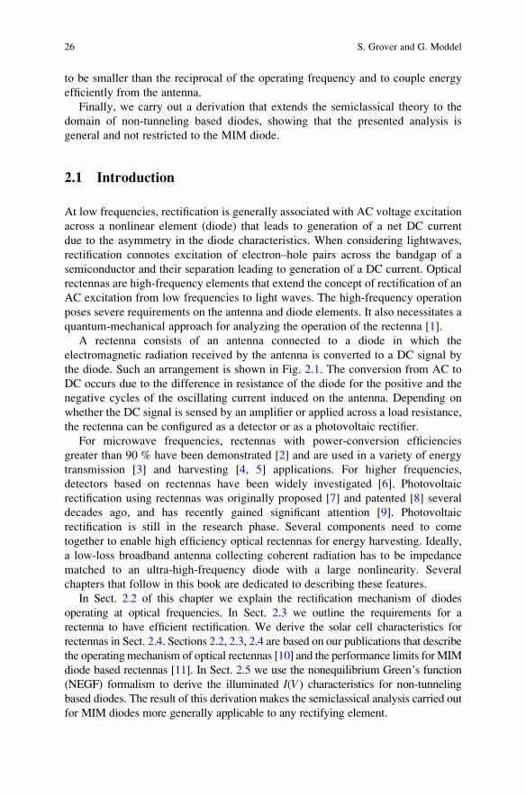
28 S. Grover and G. Moddel
of energies separated by the photon energy (�hω) as shown in Fig. 2.3. The
amplitude of the electron being found at energy E + n�hω is given by the Bessel
function of order n, where n corresponds to the number of photons absorbed or
emitted by the electron in a multiphoton process. The time dependent wavefunction
is normalized since the infinite sum of the square of Bessel terms is unity. The
electron density is proportional to the modulus squared of the wavefunction and
therefore to the square of the Bessel function.
Heuristically, the effect of the wavefunction modulation on the tunnel current is
to modulate all such single-electron states with steps of DC voltage proportional to
Vph [24]. Thus in addition to the DC voltage, there is a voltage nVph that is applied
across the diode with a weighting factor J2nðαÞ, where α ¼ eVω/Vph. The DC current
under illumination is then given by
IillumðVD;VωÞX1n¼�1
J2nðαÞIdarkðVD þ nVphÞ (2.6)
where Idark(V) is the tunnel current in the un-illuminated diode.
We use (2.6) in Sect. 2.4 to study the solar cell characteristics of rectennas.
The above derivation is based on MIM tunnel diodes. In Sect. 2.5, we derive a
generalized theory for optical rectification that extends the applicability of (2.6) to
the more general case of any mesoscopic diode operating at high frequency.
Here we limit the analysis to include illumination at a single frequency.
Characteristics of a diode illuminated by several frequencies are given in Chap. 3.
In the remaining part of this section, we discuss the ramifications of
single-frequency PAT on diode resistance and nonlinearity at optical frequencies.
The importance of the diode responsivity is discussed in Sect. 2.3.1.
Apart from the DC component of the tunnel current given by (2.6), there is a
time-dependent current that consists of the harmonics of ω that is given by [25]
Iω ¼X1
n¼�1JnðαÞ½Jnþ1ðαÞ þ Jn�1ðαÞ� IdarkðVD þ nVphÞ (2.7)
eVD
E
E+
E-
electron tunneling
x
EFig. 2.3 An electron at
energy E absorbs or emits
photons. The transmission
probability of the electron
increases at higher energies
[© IOP [10]]
2 Optical Frequency Rectification 29

Combining (2.6) and (2.7), we obtain the semiclassical diode resistance (RSCD )
and the semiclassical diode responsivity (βSCi ) using the equations [24]
RSCD ¼ Vω
Iω; βSCi ¼ ΔI
12VωIω
(2.8)
where the superscript SC denotes the use of the semiclassical PAT formulation.
The ΔI is the incremental DC current due to the illumination and is given by
ΔI ¼ Iillum � Idark.From here on we simplify the analysis by assuming α � 1 such that Bessel
function terms only up to first order in n are required. This implies a small probability
for multiple photon emission or absorption. One can mathematically verify that
higher order terms are negligible for α � 1 by using the approximation for Bessel
functions J0(α) � 1 � α2/4 and J�n(α) � (�α/2)n/(n!). This gives the ratio of Jn + 1/
Jn ¼ α/(n + 1) implying sharply decreasing contribution with increasing n at small
α. From (2.7), to first order in n(¼�1, 0, 1), RSCD is given by [25]
RSCD ¼ 2Vph
IdarkðVD þ VphÞ � IdarkðVD � VphÞ�!classical 1
I0(2.9)
which in the classical limit (�hω ! 0) leads to the differential resistance. We note
that the semiclassical resistance is the reciprocal of the slope of a secant between
two points in the I(V ) curve separated by 2Vph rather than the tangential slope at a
single point for the classical case.
The semiclassical responsivity is similarly found from the first-order
approximation of (2.6) and (2.7), and is given by [25]
βSCi ¼ 1
Vph
IdarkðVD þ VphÞ � 2IdarkðVDÞ þ IdarkðVD � VphÞIdarkðVD þ VphÞ � IdarkðVD � VphÞ
� ��!classical 1
2
I00
I0(2.10)
In the limit of small photon energies this leads to the classical formula for
responsivity given by 1/2 the ratio of second derivative of current to the first
derivative.
Classically, the diode resistance and responsivity are independent of frequency.
The semiclassical resistance and responsivity deviate from the classical values at
high photon energies. In Fig. 2.4 we plot the semiclassical resistance and
responsivity at zero bias vs. the photon energy (�hω) for a simulated diode I(V)[11]. As the photon energy increases, the resistance of the diode decreases and the
responsivity decreases. For large �hω the responsivity approaches the limit of e/�hω,which is the maximum achievable responsivity corresponding to one electron per
photon. Therefore, even a diode with poor quantum efficiency at low �hω becomes
more efficient and thus adequate at high �hω.In the next section, we discuss the impact of the semiclassical diode parameters
on the rectification efficiency and impedance matching with the antenna.
30 S. Grover and G. Moddel

2.3 Rectenna Requirements
2.3.1 Overview
The rectification efficiency (η) of a rectenna is determined by the combination of
several factors as given in (2.11) [26]. The efficiency (η) is not the same as the
conventionally accepted efficiency of a solar cell. Rather this is closer in definition
to the quantum efficiency or spectral response of a solar cell that provides the
short-circuit current produced for a given amount of input AC power. The overall
cell efficiency for rectenna solar cells is derived in Chap. 3.
η ¼ ηaηsηcηj (2.11)
where
• ηa is the efficiency of coupling the incident EM radiation to the antenna and
depends on the radiation pattern of the antenna as well as its bandwidth. Another
consideration for ηa that is important for energy harvesting is the area over which
radiation received from the source (e.g., sun) is coherent and can be captured by
a single antenna element. For the case of the sun, the coherence radius is a few
10’s of microns. Chapter 4 gives a comprehensive study of this criterion.
• ηs is the efficiency with which the collected energy propagates to the junction ofthe antenna and the diode and is largely governed by losses in the antenna, such
as resistive loss at high frequencies. For a more detailed description of antenna
efficiency, the reader is referred to Chaps. 11, 12, and 13.
Fig. 2.4 Variation of
classically and
semiclassically calculated
resistance and responsivity
vs. photon energy at
VD ¼ 0 V. As the photon
energy increases, the
semiclassical resistance
becomes significantly lower
than the classical value and
the semiclassical
responsivity approaches the
value corresponding to unity
quantum efficiency [© IEEE
[11]]
2 Optical Frequency Rectification 31

• ηc is the coupling efficiency between the antenna and the diode and requires the
antenna and the diode to be impedance matched for efficient power transfer.
Series resistance losses in the diode also need to be considered. We elaborate on
impedance matching in Sect. 2.3.2.
• ηj is the efficiency of rectifying the power received in the diode. The efficiency
of the diode junction can be expressed in terms of its current responsivity
ηj ¼ βi.
The ηj sets the overall units of η to be A/W implying the DC current produced per
watt of incident radiation. An underlying assumption in the above discussion is that
the diode has a low RC time constant and an intrinsically high speed. The low RC
time constant is needed to ensure that the AC excitation across the diode is not
shorted out due to a large diode capacitance. As we derive next, this requirement
imposes a frequency limitation on rectennas, different from the requirement for
high-speed transport of the charges.
2.3.2 Impedance Matching and RC Cutoff
The antenna-to-diode power-coupling efficiency (ηc) is given by the ratio of the ACpower delivered to the diode resistance to the power sourced by the antenna. This
ratio can be calculated from the analysis of a circuit of the rectenna shown in
Fig. 2.5. The antenna is modeled by a Thevenin equivalent and the diode by the
parallel combination of a capacitor and a voltage-dependent resistor. For simplicity
of analysis, series resistance of the diode [13] and reactance of the antenna are
assumed to be negligible.
The power-coupling efficiency at a frequency ω is given by [20]
ηc ¼PAC;RD
PA
¼4 RARD
ðRAþRDÞ2
1þ ω RARD
ðRAþRDÞCD
� �2 (2.12)
~
RA
VA
RDCD
Diode Antenna
Fig. 2.5 A small signal circuit representation of the rectenna for determining the antenna-to-diode
coupling efficiency [11]. The antenna is modeled as a voltage source in series with a resistance and
the MIM diode is modeled as a resistor in parallel with a capacitor [© IEEE [11]]
32 S. Grover and G. Moddel
where PA ¼ V2A=ð8RAÞ. In the above equation, the numerator gives the impedance
match between the antenna and the diode with RA ¼ RD leading to efficient power
transfer.
In Fig. 2.5, if the capacitive branch is open-circuit due to a small capacitance
or low frequency, the circuit is essentially a voltage divider between RA and RD.
The denominator in (2.12) determines the cutoff frequency of the rectenna, which is
based on the RC time constant determined by the resistance in parallel with antenna
the diode resistance and capacitance. Above the cutoff frequency, the capacitive
impedance of the diode is smaller than the parallel resistance, leading to inefficient
coupling of power from the antenna to the diode resistor.
As stated earlier, the responsivity form of the overall efficiency (η) indicatesthe DC current generated normalized to 1 W of incident radiation. In a PV rectifier,
the performance measure of interest is the power-conversion efficiency (ηload)which is given by the ratio of the DC power delivered to the load and the
incident AC power
ηload ¼Pload
PA
¼ I2DC;loadRload
PA
(2.13)
The IDC,load is proportional to the square of DC current dissipated in the load
implying [22]
ηload / β2i PAη2c (2.14)
Keeping aside the antenna efficiency components, the power-conversion
efficiency depends on four factors: the diode responsivity, the strength of the AC
signal that depends on the power received by the rectenna, the impedance match
between the antenna and the diode, and the RC time constant of the circuit.
Efficient coupling of power from the antenna to the diode requires impedance
matching between them. Moreover, having a small RC time constant for the circuit
implies that the product of the antenna resistance (RA) in parallel with the diode
resistance (RD) and the diode capacitance (CD) must be smaller than 1/ω for the
radiation incident on the rectenna. This ensures that the signal from the antenna
drops across the diode resistor (RD) and is not shorted out by CD. Therefore the
conditions of RD ¼ RA and ω(RA||RD)CD � 1 lead to a unity coupling efficiency,
as can be seen from (2.12). The parameters that can be varied to achieve these
conditions are the diode area, the antenna resistance, and the composition of the
diode. Obtaining a sufficiently low diode resistance to match the antenna
impedance is a challenge, and so for this analysis we choose the Ni/NiO
(1.5 nm)/Ni MIM diode, which has an extremely low resistance and was used in
several high-frequency rectennas [6, 27, 28].
Typical antenna impedances are on the order of 100 Ω [6]. We choose a nominal
antenna impedance of 377 Ω, but as will become apparent a different impedance
would not help. We vary the diode area, which changes the diode resistance and
capacitance. In Fig. 2.6, we show the ηcoupling vs. the diode edge length for a
2 Optical Frequency Rectification 33

classically and semiclassically calculated diode resistance. The semiclassical
resistance, which results from a secant between two points on the I(V ) curve, islower than the classical resistance, as shown in Fig. 2.6, and gives a higher ηcoupling.The peak in both the curves occurs at the same edge length, and is an outcome of the
balance between the needs for impedance matching and low cutoff frequency.
The coupling efficiency is limited by the combined effect of impedance
matching given by the numerator (ideally RD/RA ¼ 1) and cutoff frequency given
by the denominator (ideally ω(RA||RD)CD ¼ 0) in (2.12). Unity coupling efficiency
under the ideal conditions occurs for different edge lengths, as shown in Fig. 2.6a.
The overall efficiency is given by the smaller of the two values, limited by the two
curves in Fig. 2.7a, which leads to the peak in Fig. 2.6. Increasing the diode
resistance 10 times lowers the coupling efficiency by the same factor.
The tradeoff between impedance match to the antenna, for which a small RD is
desired, and a high cutoff frequency, for which a small CD is desired, is fundamental
for parallel-plate devices. Varying the antenna impedance results in a simple
translation of both curves in tandem such that the diode edge length for peak
efficiency changes as shown in Fig. 2.7a. With an increase in antenna impedance
a higher RD can be accommodated, allowing the diode area to be smaller, and
resulting in a desirable smaller CD. However, the higher RA also increases the
(RA||RD)CD time constant.
The condition under which the constraints simultaneously lead to a high
coupling efficiency is obtained by combining
ωðRAjjRDÞCD � 1 andRD
RA
¼ 1 ) RDCD � 2
ω(2.15)
Fig. 2.6 Effect of varying the edge length (for a square diode area) on the antenna-to-diode
coupling efficiency [11]. The peak in efficiency is due to the tradeoff between impedance match
and cutoff frequency. A simulated I(V ) curve is used to calculate the resistance of the Ni–NiO
(1.5 nm)–Ni diode using the classical and the semiclassical (Eph ¼ 1.4 eV, λair ¼ 0.88 μm) forms
of (2.9). The barrier height of Ni–NiO is 0.2 eV [28] [© IEEE [11]]
34 S. Grover and G. Moddel

For the model Ni–NiO–Ni diode discussed above, this condition is not satisfied for
near-IR frequencies (λ ¼ 0.88 μm), where 2/ω ¼ 9.4 � 10�16 s is much smaller
than RDCD ¼ 8.5 � 10�14 s. It is satisfied for wavelengths greater than 80 μm.
Due to the parallel-plate structure of the MIM diodes, the RDCD time constant is
independent of the diode area and is determined solely by the composition of the
MIM diode. As already noted, the Ni/NiO/Ni diode is an extremely low resistance
diode and NiO has a small relative dielectric constant (εr) of 17 at 30 THz. Even if
one could substitute the oxide with a material having comparable resistance and
lower capacitance (best case of εr ¼ 1), the RDCD would still be off by an order of
magnitude for near-IR operation. Putting practicality aside completely, a near-ideal
resistance would result from a breakdown-level current density of 107 A/cm2 at,
say, 0.1 V, giving a resistance of 10�8Ω-cm2. A near-ideal capacitance would result
from a vacuum dielectric separated by a relatively large 10 nm, giving a capacitance
of ~10�7 F/cm2. The resulting RDCD would be ~10�15 s, again too large for efficient
coupling at visible wavelengths.
For coupling, the relevant resistance is the differential resistance rather than the
absolute resistance. A highly nonlinear diode with a sharp turn-on at a positive
voltage would therefore give a lower resistance than what we have calculated
Fig. 2.7 Antenna-to-diode coupling efficiency as a function of diode edge length. The effect
of impedance match is separated from cutoff frequency for two antenna impedance values:
(a) RA ¼ 377 Ω, and (b) RA ¼ 10 kΩ. The parallel combination of RA and RD is denoted by RP.
The curves labeled RD/RA show the coupling efficiency when only the impedance match is the
limiting factor and those labeled ωRPCD show the coupling efficiency when only the cutoff
frequency is the limiting factor. The maximum efficiency occurs for an edge length at the small
peak where the two curves coincide [© IEEE [11]]
2 Optical Frequency Rectification 35
above. Alas, this does not help at optical frequencies because the differential
resistance in the semiclassical case is the inverse of the slope of the secant
between points that are �hω/e above and below the operating voltage. At the large
�hω of optical frequencies the secant mutes the effect of a sharp turn in the I(V )characteristics.
Several techniques are being investigated to overcome the RC constraint and
include variations on MIM diodes as well as completely new diode structures. The
coupling efficiency of MIM-diode rectennas is improved at longer wavelengths,
where the condition imposed by (2.15) is easier to meet. The RDCD can also be
artificially reduced by compensating the capacitance of the MIM diode with an
inductive element, but this is difficult to achieve over a broad spectrum. In Chap. 7,
a sharp tip MIM diode is described that can potentially reduce the capacitance while
maintaining a low resistance. A design that can circumvent the restrictions imposed
on the coupling efficiency is the MIM traveling-wave rectifier [21, 29]. Akin to a
transmission line where the geometry determines the impedance, the distributed RC
enhances the coupling between the antenna and the traveling-wave structure.
However, losses in the metallic regions of the waveguide limit its efficiency as
the frequency approaches that of visible light.
A new type of diode called the geometric diode is described in Chap. 10 and can
potentially satisfy the requirements of low resistance and capacitance. It rectifies
based on a nanoscale asymmetry in the shape of the conducting material that leads
to a preferential direction for flow of charge carriers. The absence of a tunneling
barrier leads to an extremely low resistance. The planar structure of the geometric
diode lifts the capacitance constraint imposed by the parallel-plate structure of the
MIM diode.
2.4 Operation at Optical Frequency
In this section we use the PAT theory developed in Sect. 2.2 to derive the
illuminated I(V ) characteristics of ideal diodes, i.e., for the case of an illuminated
rectenna. The power-generating regime is shown to occur in the second quadrant
of the I(V ) curve. We assume that a constant AC voltage is applied across the diode
as the DC bias voltage is varied. This assumption helps to develop the
understanding of how an illuminated I(V ) curve can be obtained starting with
dark I(V ) using (2.6). In practice, the magnitude of the AC voltage would vary
with the DC bias as explained and dealt with in Chap. 3. Due to the dependence of
the diode resistance on AC voltage as given by (2.9), the two assumptions lead to
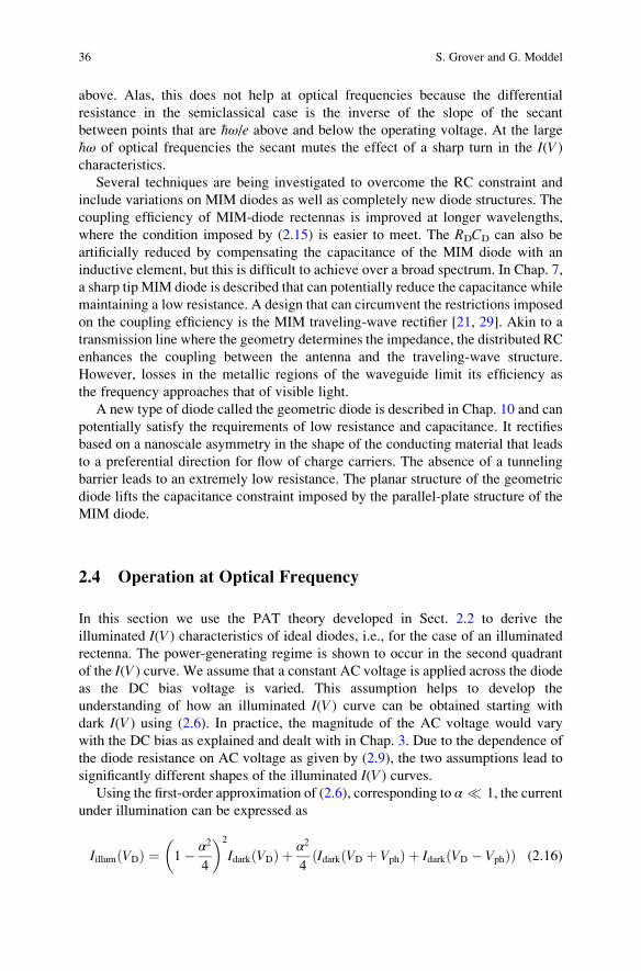
significantly different shapes of the illuminated I(V ) curves.Using the first-order approximation of (2.6), corresponding to α � 1, the current
under illumination can be expressed as
IillumðVDÞ ¼ 1� α2
4
� �2
IdarkðVDÞ þ α2
4ðIdarkðVD þ VphÞ þ IdarkðVD � VphÞÞ (2.16)
36 S. Grover and G. Moddel

with the first term on the right-hand side representing the dark current due to
electrons that are in the unexcited state. The second and third terms represent the
current resulting from electrons that undergo a net absorption or emission of a
photon, respectively, together denoted as ΔI. To understand the effect of ΔI onIillum, consider an ideal diode with the piecewise linear Idark shown in Fig. 2.8a.
As shown in Fig. 2.8b, the two terms in ΔI modify Idark such that a positive current
can flow even at zero or a negative DC bias. The sum of the three current
components of (2.16) is shown in Fig. 2.8c with power generation occurring in
the second-quadrant operation of the diode (in contrast to the fourth-quadrant for a
conventional solar cell). The DC current generated depends on Vω via α and thereby
the strength of the illumination and the antenna design.
In the illuminated I(V ) curve shown in Fig. 2.8c the voltage-intercept is marked
as Vph, which signifies the maximum negative voltage at which a positive current is
possible. This occurs for a diode with a high forward-to-reverse current ratio.
As seen in the second quadrant of Fig. 2.8c, the triangular illuminated I(V ),under the assumption of constant Vω, incorrectly suggests a peak efficiency of only
25 %. In Chap. 3, we show that the maximum theoretical efficiency for rectification
of monochromatic illumination is 100 %.
V
I
V
I
I
Vph Vph
Vph
Vph
V
Idark(VD)
Iillum(VD)
J02
J12
Idark(VD)
J-12
Idark(VD+Vph)
Idark(VD-Vph)
a
b
c
Fig. 2.8 (a) Piecewise linear
dark I(V ) curve. (b) Scaledand voltage-shifted
components of Iillum as given
by (2.16) under the
assumption of constant AC
input voltage. (c) Illuminated
I(V ) curve obtained by
adding the components in
(b). The region of positive
current at negative voltage
corresponds to power
generation [© IOP [10]]
2 Optical Frequency Rectification 37

2.5 Optical Frequency Rectification in Mesoscopic Diodes
In the semiclassical analysis for the optical response of an MIM diode presented in
Sect. 2.2, the I(V) characteristics under illumination are obtained from the DC dark
I(V ) curve of the diode. To make the operating mechanism of optical rectennas,
derived in the previous section, valid for a broader class of diodes a derivation
similar to the Tien and Gordon approach [23], but generalized to be applicable even
to a non-tunneling based device, is required. Such a theory is presented here [1] and
is applicable, for example, to the geometric diode described in Chap. 10.
A mesoscopic junction is categorized as having length-scales comparable to the
electron phase coherence length [30]. An asymmetric mesoscopic junction can
show rectification due to interaction of carriers with the conductor boundaries.
Rectification in such junctions was predicted to occur due to an asymmetric
conductor or an asymmetric illumination in a symmetric conductor [31]. At least
one of these two conditions is necessary. Photovoltaic effect has been observed in
small conductors having geometric asymmetry due to disorder [32] or patterned
asymmetric shapes [1].
Platero and Aguado [33] have reviewed several techniques that can be used to
study photon-assisted transport in semiconductor nanostructures. Other than Tien
and Gordon’s approach, all the analyses culminate in a form requiring numerical
computation of the transport mechanism, and do not provide insights into the
optical behavior through a simple extension of the DC characteristics.
The simplicity of the Tien and Gordon formulation comes with the drawback
that the theory is not gauge-invariant. Another limitation of this method is that it
does not account for charge and current conservation. To ensure conservation, an
AC transport theory such as the one that solves the NEGF and Poisson equations
self-consistently [34] is required. In a geometric diode, the dependence of the
transport properties on the geometry adds to the complexity.
Here we use the NEGF formulation to derive an equation analogous to Tien and
Gordon’s equation given by (2.6) but also applicable to an illuminated mesoscopic
junction. Starting with the Hamiltonian that describes the material and the structure
of the geometric diode, the NEGF approach is used to model geometry-dependent
transport, and interaction of electrons with an AC voltage.
Several approximations are made to enable an analytical relation between the
DC and illuminated characteristics. Even though these approximations limit the
region of applicability of the result, it is nevertheless helpful in understanding
the illuminated characteristics of mesoscopic junctions.
2.5.1 Mesoscopic Junction Under Illumination
The starting point for the derivation is the NEGF theory for an illuminated junction
given by Datta and Anantram [35]. In this section we reproduce and explain some
of their results.
38 S. Grover and G. Moddel

Consider a mesoscopic junction connected to two contacts, as shown in Fig. 2.9.
It is assumed that charge transport from one contact to the other occurs
phase-coherently, and the coherence is broken only by scattering in the contacts.
Here, the contacts refer to charge reservoirs, much larger than the device region,
held at a fixed potential. Electrons gain or lose energy through scattering in the
contacts. The interaction of charge carriers with photons occurs in the device region
through a time-varying potential V(~r ,t). This interaction, even though inelastic
(changes the energy of charge particles), does not cause phase incoherence.
The energy-domain version of Schrodinger’s equation for the device in the
absence of illumination is [35]
Eþ �h2r2
2m � VSð~rÞ þ i�h2τφð~r;EÞ
h iGR
0 ð~r;E;~r 0;E0Þ ¼ δð~r �~r 0ÞδðE� E0Þ) H0ð~r;EÞGR
0 ð~r;E;~r 0;E0Þ ¼ δð~r �~r 0ÞδðE� E0Þ(2.17)
where GR0 is the retarded Green’s function that represents the impulse response of
Schrodinger’s equation. The subscript ‘0’ refers to the Green’s function for the
un-illuminated case. The wavefunction at any energy E can be obtained fromGR0 . Vs
is the static potential in the device. The τφ is the scattering (phase-breaking) time in
the contacts.
The current in the device is obtained as
I ¼ e�h
ZdE
ZdE0Z
d~r
Zd~r 0½t21ðE;E0Þf1ðE0Þ � t12ðE0;EÞf2ðEÞ� (2.18)
where f1 and f2 are the Fermi-Dirac distributions in contact 1 and 2 respectively.
The t21(E,E0) is the transmission from an input energy mode E0 in contact 1 to an
output energy mode E in contact 2, and is given by
t21ðE;E0Þ ¼ �h
τavg
ð ð~r2contact1~r 02contact2
d~rd~r 0jGRð~r;E;~r 0;E0Þj2
4π2τφð~r;EÞτφð~r 0;E0Þ (2.19)
Contact 1: 1 Contact 2: 2Junction: V( r,t)
Fig. 2.9 A two terminal
device with an arbitrary
shape, subjected to an AC
potential V(~r,t)
2 Optical Frequency Rectification 39

The τavg is the time over which the current or the transmission is averaged to find
the DC component. The un-illuminated case is obtained by replacing GR by GR0 in
(2.19).
Equation (2.18) is different from the usual form for the transport equation that
takes into account the exclusion principle by counting the filled states on one
contact and the empty states on the other. The applicability of this equation for
phase-coherent transport is explained by Landauer [36] and the equation is
explicitly derived by Datta and Anantram [35].
Under illumination, the Schrodinger equation is modified as [35, 37]
H0ð~r;EÞGRð~r;E;~r 0;E0Þ ¼ δð~r �~r 0ÞδðE� E0ÞþXω
Vð~r; �hωÞGRð~r;E� �hω;~r 0;E0Þ (2.20)
where V(~r,t) is represented by its Fourier transform componentsP
Vð~r; �hωÞ. Thisperturbation term added to the RHS is the strength of the broadening due to
interaction with the field [38]. This effect is included via a self-energy similar to
the one used for contacts [34]. Under a first-order Born approximation, the solution
to the equation of motion given by the modified Schrodinger equation in (2.20), is
GRð~r;E;~r 0;E0Þ ¼ GR0 ð~r;~r 0;EÞδðE� E0Þ
þXω
Zd~r 00GR
0 ð~r;~r 00;EÞVð~r 00; �hωÞGR0 ð~r 00;~r 0;E0ÞδðE� �hω� E0Þ (2.21)
In the presence of illumination, the current is obtained by substituting GR in
(2.19) by the expression in (2.21). The GR can be computed numerically using the
technique described in Chap. 7. However in the next section, we simplify (2.21)
such that the illuminated characteristics can be predicted by an analytical extension
of the DC I(V ) curve.
2.5.2 Projecting Illuminated Characteristics from DC I(V)
We propose two simplifications to the expression forGR given in (2.21). The first is a
uniform strength of interaction with the field over the device area (V(~r,�hω) ¼ V(�hω)).This is achieved by coupling an AC scalar potential through a gate electrode [39] or
by applying the dipole approximation for a vector potential gauge [22]. The dipole
approximation requires that the wavelength of the EM field be much larger than
the size of the device. This condition is easily satisfied for a MIM diode, and for
small geometric diodes. A further complication in geometric diodes is the field
nonuniformity due to the shape of the conductor. For this, a field strength averaged
over the geometry would serve as an initial correction.
40 S. Grover and G. Moddel
The second approximation relates to the transport properties of electrons at
energies separated by �hω. Here, we claim that the transport properties defined by
GR do not differ significantly for two energy levels spaced apart by �hω. The GR for
the two energies are similar if the photon energy is small compared to the energy of
electrons. As the majority of conduction occurs due to electrons at the Fermi
surface, the relevant energy for comparison is the Fermi energy (�hω � Ef)
measured with respect to the band edge. This assumption is similar to the nearly
elastic scattering case considered by Datta [38]. The ramifications of this
approximation are discussed at the end of the chapter.
Under these assumptions, (2.21) is simplified to
GRð~r;E;~r 0;E0Þ ¼ GR0 ð~r;~r 0;EÞδðE� E0Þ
þXω
Vð�hωÞZ
d~r 00GR0 ð~r;~r 0;EÞδðE� �hω� E0Þ (2.22)
where the Green’s function in the integral is simplified under the assumption
E � E0 as
GR0 ð~r;~r 0;EÞ ¼ GR
0 ð~r;~r 00;EÞGR0 ð~r 00;~r 0;E0Þ (2.23)
The spatial integral on the RHS of (2.22) leads to the volume of the device region
(vol.) as there is no dependence on~r 00 in the integrand. The Green’s function underillumination then becomes
GRð~r;E;~r 0;E0Þ ¼ GR0 ð~r;~r 0;EÞδðE� E0Þ
þ vol:Xω
Vð�hωÞGR0 ð~r;~r 0;EÞδðE� �hω� E0Þ (2.24)
Substituting the above expression in (2.19)
t21ðE;E0Þ / GR0 ð~r;~r 0;EÞδðE� E0Þ þ vol:
Xω
Vð�hωÞGR0 ð~r;~r 0EÞδðE� �hω� E0Þ
����������2
¼ jGR0 ð~r;~r 0EÞj2δ2ðE� E0Þ
þ GR0 ð~r;~r 0;EÞδðE� E0Þ þ vol:
Xω
Vð�hωÞGR0 ð~r;~r 0;EÞδðE� �hω� E0Þ
!ccþ cc
" #
þ vol:Xω
Vð�hωÞGR0 ð~r;~r 0;EÞδðE� �hω� E0Þ
����������2
(2.25)
2 Optical Frequency Rectification 41

where cc denotes complex conjugate. The term inside the square bracket has a
product of two delta-functions δ(E � E0)*δ(E � �hω � E0), which is always zero.
Also, in the third term, the square of the summation over delta-functions is equal to
the summation of the squares as all cross terms with different ω are always zero due
to the product of delta-functions δ(E � �hω1 � E0)*δ(E � �hω2 � E0). Therefore(2.25) reduces to
t21ðE;E0Þ / jGR0 ð~r;~r 0;EÞj2δðE� E0Þ þ Vol�X
ω
jVð�hωÞj2jGR0 ð~r;~r 0;EÞj2δðE� �hω� E0Þ (2.26)
The second term in the above equation represents a first-order,
low-photon-energy correction to the Green’s function for the un-illuminated case.
This leads to the expression for illum given by
Iillum ¼ e�h2
T
ZdE
ZdE0Z~r2
d~r
Z~r1
d~r 0
�
jGR0 ð~r;~r 0;EÞj2δðE� E0Þ4π2τφð~r;EÞτφð~r 0;E 0Þ f1ðE 0Þ � jGR
0 ð~r 0;~r;E 0Þj2δðE 0 � EÞ4π2τφð~r;EÞτφð~r 0;E 0Þ f2ðEÞ
þ vol:2Xω
jVð�hωÞj2jGR
0 ð~r;~r 0;EÞj2δðE� �hω� E 0Þ4π2τφð~r;EÞτφð~r 0;E 0Þ f1ðE 0Þ
� jGR0 ð~r 0;~r;EÞj2δðE 0 � �hω� EÞ4π2τφð~r;EÞτφð~r 0;E 0Þ f2ðEÞ
8>>>><>>>>:
9>>>>=>>>>;
266666666664
377777777775
(2.27)
We now perform the integral with respect to E0 in (2.27) using the sifting
property of the delta function. Under the condition �hω � Ef, we also
approximate that τφ does not vary significantly from E to E + �hω. The validity of
this is in-line with the approximation made for GR in that the interaction of an
electron with the reservoirs is similar at two closely spaced energies. With this
simplification, the illum is given by
Iillum ¼ e�h2
T
RdER~r2d~rR~r1d~r 0
�
jGR0 ð~r;~r 0;EÞj2
4π2τφð~r;EÞτφð~r 0;EÞ f1ðEÞ �jGR
0 ð~r 0;~r;E 0Þj24π2τφð~r;EÞτφð~r 0;EÞ f2ðEÞ
þ vol:2Xω
jVð�hωÞj2jGR
0 ð~r;~r 0;EÞj24π2τφð~r;EÞτφð~r 0;EÞ f1ðE� �hωÞ
� jGR0 ð~r 0;~r;EÞj2δðE 0 � �hω� EÞ4π2τφð~r;EÞτφð~r 0;E 0Þ f2ðEÞ
8>>>>><>>>>>:
9>>>>>=>>>>>;
2666666666664
3777777777775
(2.28)
42 S. Grover and G. Moddel

which can be simplified to
Iillum ¼ e�h2
T
RdER~r2d~rR~r1d~r 0
�
jGR0 ð~r;~r 0;EÞj2
4π2τφð~r;EÞτφð~r 0;EÞ ff1ðEÞ � f2ðEÞg
þ vol:2Xω
jVð�hωÞj2 jGR0 ð~r;~r 0;EÞj2
4π2τφð~r;EÞτφð~r 0;EÞ ff1ðE� �hωÞ � f2ðEÞg
266664
377775
(2.29)
The second term in the above equation that represents the additional current due
to illumination and can be written in terms of the un-illuminated (dark) current given
by the first term. This is done by combining the �hω with the DC voltage applied
between the two contacts (VD). Assuming that contact 2 is the ground, (2.29) can be
written in terms of the Fermi distribution f(E) ¼ [1 + exp((E � Ef)/kT)]�1 as
Iillum ¼ e�h2
T
RdER~r2d~rR~r1d~r 0
�
jGR0 ð~r;~r 0;EÞj2
4π2τφð~r;EÞτφð~r 0;EÞ ff ðE� eVDÞ � f ðEÞg
þ vol:2Xω
jVð�hωÞj2 jGR0 ð~r;~r 0;EÞj2
4π2τφð~r;EÞτφð~r 0;EÞ ff ðE� ðeVD þ �hωÞÞ � f ðEÞg
266664
377775(2.30)
This can be interpreted as
IillumðVDÞ ¼ IdarkðVDÞ þ vol:2Xω
jVð�hωÞj2Idark VD þ �hω
e
� �(2.31)
2.5.3 Discussion
Equation (2.31) allows an analytical evaluation of the illuminated characteristics
from a dark I(V ) curve, similar to the first-order approximation of (2.6) depicted
graphically using a piecewise linear dark I(V ) curve in Fig. 2.8. Although the
equation for an MIM diode was derived for a single-frequency illumination, its
multispectral extension also consists of an integral over the contribution from
different frequencies [24].
In analogy with the high-frequency operating mechanism described for an MIM
diode in Fig. 2.2, (2.31) indicates that the interaction of the electrons in the device
region is equivalent to the modulation of electron energies in the contact. This
simplified picture for the interaction emerges because the electronic transport
2 Optical Frequency Rectification 43

properties are assumed to be constant in a narrow range of energies given by the
additional photon energy (�hω) acquired by the electrons in the device region. The
derivation presented here essentially transferred the electron interaction with
the photon from the device region to the contacts.
The assumption of �hω � Ef is the most significant consideration of the
derivation. Earlier, we stated this condition without analyzing its physical
significance. Transport properties, e.g., tunneling probability in an MIM diode,
can be a strong function of energy. However, in the case of MIM diodes the
photon–electron interaction occurs only in the contacts due to the absence of
electrons in the insulator. This is the basis for the semiclassical theory described
in Sect. 2.2. In a mesoscopic junction like the geometric diode, due to the absence of
an energy barrier the transmission is a weaker function of energy than in MIM
diodes. Therefore, in narrow energy ranges, the assumption of constant transport
behavior has greater validity. Ultimately, the effect of the added photon energy is
relative to the existing electron-energy. If this energy is large, such that the
transmission is highly likely, the change in transmission by adding photon energy
will be small. A measure of validity for the existing electron energy is the Fermi
level and hence the condition �hω � Ef.
A final point of discussion concerns the material for the thin-film used in the
device region. Equation (2.31) is applicable under the assumption that the photon
energy (Eph) is small compared to the Fermi level (Ef). This depends on the value of
the Ef. For metals, Ef is on the order of a few electron-volts so that the result holds
even at far-to-mid-infrared. However, for a material like graphene, the Ef is closer
to zero, but can be varied by applying a gate-voltage or by doping.
In summary, we have shown that the I(V ) characteristics for a general
mesoscopic junction can be described by a formalism similar to that used for
MIM diodes, within the limits of some assumptions. Therefore the optical
frequency rectification analysis that was presented in this chapter applies not just
to MIM diodes but also to a wider range of optical frequency rectifiers.
References
1. Grover S. Diodes for optical rectennas. PhD Thesis, University of Colorado, Boulder; 2011.
2. Brown WC. Optimization of the efficiency and other properties of the rectenna element. 1976.
p. 142–4.
3. Shinohara N, Matsumoto H. Experimental study of large rectenna array for microwave energy
transmission. IEEE Trans Microw Theory Tech. 1998;46(3):261–8.
4. Hagerty JA, Helmbrecht FB, McCalpin WH, Zane R, Popovic ZB. Recycling ambient
microwave energy with broad-band rectenna arrays. IEEE Trans Microw Theory Tech.
2004;52(3):1014–24.
5. Singh P, Kaneria S, Anugonda VS, Chen HM, Wang XQ, et al. Prototype silicon micropower
supply for sensors. IEEE Sens J. 2006;6(1):211–22.
6. Fumeaux C, Herrmann W, Kneubuhl FK, Rothuizen H. Nanometer thin-film Ni-NiO-Ni
diodes for detection and mixing of 30 THz radiation. Infrared Phys Technol. 1998;39
(3):123–83.
44 S. Grover and G. Moddel

7. Bailey RL. A proposed new concept for a solar-energy converter. J Eng Power.
1972;94(2):73–77.
8. Marks AM. Device for conversion of light power to electric power. US Patent No. 4445050;
1984.
9. Berland B. Photovoltaic technologies beyond the horizon: optical rectenna solar cell, NREL
report no. SR-520-33263, final report; 2003.
10. Grover S, Joshi S, Moddel G. Theory of operation for rectenna solar cells. J Phys D. 2013.
11. Grover S, Moddel G. Applicability of metal/insulator/metal (MIM) diodes to solar rectennas.
IEEE J Photovoltaics. 2011;1(1):78–83.
12. Sedra AS, Smith KC. Microelectronic circuits. 4th ed. New York: Oxford University Press;
1997.
13. Yoo T, Chang K. Theoretical and experimental development of 10 and 35 GHz rectennas.
IEEE Trans Microw Theory Tech. 1992;40(6):1259–66.
14. Brown ER. A system-level analysis of Schottky diodes for incoherent THz imaging arrays.
Solid State Electron. Mar 2004;48:2051–3.
15. Kazemi H, Shinohara K, Nagy G, Ha W, Lail B, et al. First THz and IR characterization of
nanometer-scaled antenna-coupled InGaAs/InP Schottky-diode detectors for room
temperature infrared imaging. Infrared Technol Appl XXXIII. 2007;6542(1):65421.
16. Hubers H-W, Schwaab GW, Roser HP. Video detection and mixing performance of GaAs
Schottky-barrier diodes at 30 THz and comparison with metal-insulator-metal diodes, J Appl
Phys. 1994;75(8):4243–8.
17. Hartman TE. Tunneling of a wave packet. J Appl Phys. Dec 1962;33(12):3427–33.
18. Nagae M. Response time of metal-insulator-metal tunnel junctions. Jpn J Appl Phys. 1972;11
(11):1611–21.
19. Rockwell S, Lim D, Bosco BA, Baker JH, Eliasson B, et al. Characterization and modeling of
metal/double-insulator/metal diodes for millimeter wave wireless receiver applications. In
Radio frequency integrated circuits (RFIC) symposium, IEEE, Honolulu, HI; 2007. p. 171–4.
20. Sanchez A, Davis CF, Liu KC, Javan A. The MOM tunneling diode: theoretical estimate of its
performance at microwave and infrared frequencies. J Appl Phys. 1978;49(10):5270–7.
21. Grover S, Dmitriyeva O, Estes MJ, Moddel G. Traveling-wave metal/insulator/metal diodes
for improved infrared bandwidth and efficiency of antenna-coupled rectifiers. IEEE Trans
Nanotechnol. 2010;9(6):716–22.
22. Eliasson BJ. Metal-insulator-metal diodes for solar energy conversion. PhD Thesis, University
of Colorado at Boulder, Boulder; 2001.
23. Tien PK, Gordon JP. Multiphoton process observed in the interaction of microwave fields with
the tunneling between superconductor films. Phys Rev. 1963;129(2):647–51.
24. Tucker JR, Feldman MJ. Quantum detection at millimeter wavelengths. Rev Mod Phys.
1985;57(4):1055–113.
25. Tucker JR. Quantum limited detection in tunnel junction mixers. IEEE J Quantum Electron.
1979;QE-15(11):1234–58.
26. Michael Kale B. Electron tunneling devices in optics, Opt Eng. 1985;24(2):267–74.
27. Wilke I, Oppliger Y, Herrmann W, Kneubuhl FK. Nanometer thin-film Ni-NiO-Ni diodes for
30 THz radiation. Appl Phys Mater Sci Process. Apr 1994;58(4):329–41.
28. Hobbs PC, Laibowitz RB, Libsch FR, LaBianca NC, Chiniwalla PP. Efficient
waveguide-integrated tunnel junction detectors at 1.6 μm, Opt Express. 2007;15
(25):16376–89.
29. Estes MJ, Moddel G. Surface plasmon devices. US Patent 7,010,183; 2006.
30. Fal’ko V. Nonlinear properties of mesoscopic junctions under high-frequency field irradiation.
Europhys Lett. 1989;8(8):785–9.
31. Datta S. Steady-state transport in mesoscopic systems illuminated by alternating fields. Phys
Rev B. 1992;45(23):13761–4.
32. Liu J, Giordano N. Nonlinear response of a mesoscopic system. Phys
B. 1990;165&166:279–80.
33. Platero G, Aguado R. Photon-assisted transport in semiconductor nanostructures. Phys Rep.
2004;395(1–2):1–157.
2 Optical Frequency Rectification 45

34. Kienle D, Vaidyanathan M, Leonard F. Self-consistent ac quantum transport using
nonequilibrium Green functions. Phys Rev B. 2010;81:115455.
35. Datta S, Anantram MP. Steady-state transport in mesoscopic systems illuminated by
alternating fields. Phys Rev B. 1992;45(23):13761–4.
36. Landauer R. Johnson-Nyquist noise derived from quantum mechanical transmission. Phys
D. 1989;38:226–9.
37. Ferry DK, Goodnick SM, Bird J. Transport in nanostructures. 2nd ed. Cambridge: Cambridge
University Press; 2009.
38. Datta S. Quantum transport: atom to transistor. Cambridge: Cambridge University Press; 2005.
39. Pedersen MH, Buttiker M. Scattering theory of photon-assisted electron transport. Phys Rev
B. 1998;58(19):12993–3006.
40. Dagenais M, Choi K, Yesilkoy F, Chryssis AN, Peckerar MC. Solar spectrum rectification
using nano-antennas and tunneling diodes. Proc SPIE. 2010;7605:76050E–1.
46 S. Grover and G. Moddel