chapter 10: design options of digital systems 10: design options of digital systems digital system...
TRANSCRIPT

Chapter 10: Design Options of Digital Systems
Digital System Designs and Practices Using Verilog HDL and FPGAs @ 2008~2010, John Wiley 10-1
Chapter 10: Design Options of Digital Systems
Department of Electronic Engineering
National Taiwan University of Science and Technology
Prof. Ming-Bo Lin

Chapter 10: Design Options of Digital Systems
Digital System Designs and Practices Using Verilog HDL and FPGAs @ 2008~2010, John Wiley 10-2
Syllabus
ObjectivesDesign options of digital systemsPLD modelingCPLDFPGAPractical issues

Chapter 10: Design Options of Digital Systems
Digital System Designs and Practices Using Verilog HDL and FPGAs @ 2008~2010, John Wiley 10-3
ObjectivesAfter completing this chapter, you will be able to:
Describe the features of system-level design optionsDescribe basic structures and features of cell-based ASICsDescribe basic structures and features of gate array ASICsDescribe basic structures and features of programmable logic devices (PLDs)Describe basic structures and features of field-programmable gate arrays (FPGAs)Understand how to model PLAs (including PLDs)Understand the issues of voltage tolerance and voltage compliance

Chapter 10: Design Options of Digital Systems
Digital System Designs and Practices Using Verilog HDL and FPGAs @ 2008~2010, John Wiley 10-4
Syllabus
ObjectivesDesign options of digital systems
Design optionsCell-based designsGate-array-based designsField-programmable devices
PLD modelingCPLDFPGAPractical issues

Chapter 10: Design Options of Digital Systems
Digital System Designs and Practices Using Verilog HDL and FPGAs @ 2008~2010, John Wiley 10-5
Design Options of Digital Systems

Chapter 10: Design Options of Digital Systems
Digital System Designs and Practices Using Verilog HDL and FPGAs @ 2008~2010, John Wiley 10-6
System-Level Design Options
PCB (printed-circuit board)-based platformsSoPC (System on a programmable chip)-based platforms
Also called programmable system chip (PSC)
Soft IP+ cell_library-based platforms

Chapter 10: Design Options of Digital Systems
Digital System Designs and Practices Using Verilog HDL and FPGAs @ 2008~2010, John Wiley 10-7
PCB-Based Platforms
Consist of discrete standard components µP/µC, peripherals, and memory devices
NRE cost low
May need additional CPLD/FPGA devices Examples
8051PICARM family

Chapter 10: Design Options of Digital Systems
Digital System Designs and Practices Using Verilog HDL and FPGAs @ 2008~2010, John Wiley 10-8
SoPC-Based Platforms
Consist of hard or soft IPsMay need additional customized logic modules Examples
Xilinx VirtexII proSpartan 3 (MicroBlaze)Altera Cyclone Series (NIOS)

Chapter 10: Design Options of Digital Systems
Digital System Designs and Practices Using Verilog HDL and FPGAs @ 2008~2010, John Wiley 10-9
Soft IP+ Cell Library-Based platforms
Consist of soft IP being configured into an optimized system hardwareAn example
Tensilica’s Xtensa

Chapter 10: Design Options of Digital Systems
Digital System Designs and Practices Using Verilog HDL and FPGAs @ 2008~2010, John Wiley 10-10
Design Alternatives of Digital Systems

Chapter 10: Design Options of Digital Systems
Digital System Designs and Practices Using Verilog HDL and FPGAs @ 2008~2010, John Wiley 10-11
Comparison of Design Options

Chapter 10: Design Options of Digital Systems
Digital System Designs and Practices Using Verilog HDL and FPGAs @ 2008~2010, John Wiley 10-12
Syllabus
ObjectivesDesign options of digital systems
Design optionsCell-based designsGate-array-based designsField-programmable devices
PLD modelingCPLDFPGAPractical issues
Chapter 10: Design Options of Digital Systems
Digital System Designs and Practices Using Verilog HDL and FPGAs @ 2008~2010, John Wiley 10-13
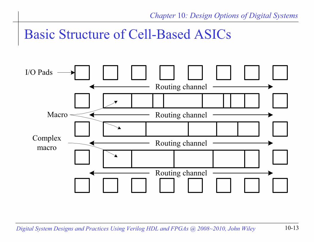
Basic Structure of Cell-Based ASICs
Routing channel
Macro
I/O Pads
Complexmacro
Routing channel
Routing channel
Routing channel

Chapter 10: Design Options of Digital Systems
Digital System Designs and Practices Using Verilog HDL and FPGAs @ 2008~2010, John Wiley 10-14
Basic Cell Types

Chapter 10: Design Options of Digital Systems
Digital System Designs and Practices Using Verilog HDL and FPGAs @ 2008~2010, John Wiley 10-15
A Cell-Based D-Type Flip Flop

Chapter 10: Design Options of Digital Systems
Digital System Designs and Practices Using Verilog HDL and FPGAs @ 2008~2010, John Wiley 10-16
Syllabus
ObjectivesDesign options of digital systems
Design optionsCell-based designsGate-array-based designsField-programmable devices
PLD modelingCPLDFPGAPractical issues

Chapter 10: Design Options of Digital Systems
Digital System Designs and Practices Using Verilog HDL and FPGAs @ 2008~2010, John Wiley 10-17
Basic Structures of Gate-Array ASICs

Chapter 10: Design Options of Digital Systems
Digital System Designs and Practices Using Verilog HDL and FPGAs @ 2008~2010, John Wiley 10-18
Basic Structures of Gate Arrays

Chapter 10: Design Options of Digital Systems
Digital System Designs and Practices Using Verilog HDL and FPGAs @ 2008~2010, John Wiley 10-19
Basic Structures of Gate Arrays

Chapter 10: Design Options of Digital Systems
Digital System Designs and Practices Using Verilog HDL and FPGAs @ 2008~2010, John Wiley 10-20
Syllabus
ObjectivesDesign options of digital systems
Design optionsCell-based designsGate-array-based designsField-programmable devices
PLD modelingCPLDFPGAPractical issues

Chapter 10: Design Options of Digital Systems
Digital System Designs and Practices Using Verilog HDL and FPGAs @ 2008~2010, John Wiley 10-21
Shorthand Notations
Chapter 10: Design Options of Digital Systems
Digital System Designs and Practices Using Verilog HDL and FPGAs @ 2008~2010, John Wiley 10-22
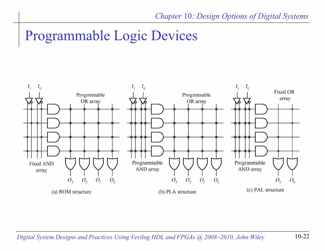
Programmable Logic Devices

Chapter 10: Design Options of Digital Systems
Digital System Designs and Practices Using Verilog HDL and FPGAs @ 2008~2010, John Wiley 10-23
Basic Structures of CPLDs

Chapter 10: Design Options of Digital Systems
Digital System Designs and Practices Using Verilog HDL and FPGAs @ 2008~2010, John Wiley 10-24
Basic Structures of FPGAs

Chapter 10: Design Options of Digital Systems
Digital System Designs and Practices Using Verilog HDL and FPGAs @ 2008~2010, John Wiley 10-25
Basic Structures of PICs

Chapter 10: Design Options of Digital Systems
Digital System Designs and Practices Using Verilog HDL and FPGAs @ 2008~2010, John Wiley 10-26
Comparison of PICs

Chapter 10: Design Options of Digital Systems
Digital System Designs and Practices Using Verilog HDL and FPGAs @ 2008~2010, John Wiley 10-27
Syllabus
ObjectivesDesign options of digital systemsPLD modeling
ROM /PLA /PALPLA modeling
CPLDFPGAPractical issues

Chapter 10: Design Options of Digital Systems
Digital System Designs and Practices Using Verilog HDL and FPGAs @ 2008~2010, John Wiley 10-28
Basic Structures of ROMs

Chapter 10: Design Options of Digital Systems
Digital System Designs and Practices Using Verilog HDL and FPGAs @ 2008~2010, John Wiley 10-29
Basic Structures of PLAs

Chapter 10: Design Options of Digital Systems
Digital System Designs and Practices Using Verilog HDL and FPGAs @ 2008~2010, John Wiley 10-30
Basic Applications of PLAs

Chapter 10: Design Options of Digital Systems
Digital System Designs and Practices Using Verilog HDL and FPGAs @ 2008~2010, John Wiley 10-31
A PAL Example --- 16R8

Chapter 10: Design Options of Digital Systems
Digital System Designs and Practices Using Verilog HDL and FPGAs @ 2008~2010, John Wiley 10-32
Syllabus
ObjectivesDesign options of digital systemsPLD modeling
ROM /PLA /PALPLA modeling
CPLDFPGAPractical issues

Chapter 10: Design Options of Digital Systems
Digital System Designs and Practices Using Verilog HDL and FPGAs @ 2008~2010, John Wiley 10-33
PLA Modeling
PLA device structures SOP (sum of product) = AND plane + OR plane
• AND plus OR array• NAND plus NAND array
POS (product of sum) = OR plane + AND plane• OR plus AND array• NOR plus NOR array
An AND plane or an OR plane a personalityarray (or memory)

Chapter 10: Design Options of Digital Systems
Digital System Designs and Practices Using Verilog HDL and FPGAs @ 2008~2010, John Wiley 10-34
PLA Modeling
A PLA device is modeled bya group of system tasksan appropriate combination of two system tasks
A PLA device can be modeled as:AsynchronousSynchronous

Chapter 10: Design Options of Digital Systems
Digital System Designs and Practices Using Verilog HDL and FPGAs @ 2008~2010, John Wiley 10-35
PLA Modeling

Chapter 10: Design Options of Digital Systems
Digital System Designs and Practices Using Verilog HDL and FPGAs @ 2008~2010, John Wiley 10-36
PLA Modeling
wire a1, a2, a3, a4, a5, a6, a7;reg b1, b2, b3;wire [1:7] awire;reg [1:3] breg;reg [1:7] mem [1:3]; // define personality memory
// asynchronous AND plane$async$and$array(mem, {a1, a2, a3, a4, a5, a6, a7}, {b1, b2, b3});// or using the following statement$async$and$array(mem, awire, breg);// synchronous AND planeforever @(posedge clock)
$sync$and$array(mem, {a1, a2, a3, a4, a5, a6, a7}, {b1, b2, b3});
$async$logic$array(mem_type, input_terms, output_terms);$sync$logic$array(mem_type, input_terms, output_terms);

Chapter 10: Design Options of Digital Systems
Digital System Designs and Practices Using Verilog HDL and FPGAs @ 2008~2010, John Wiley 10-37
Logic Array Personality
Defined as an array of regWidth: the number of input termsDepth: the number of output terms
Loaded into memory usingSystem tasks $readmemb or $readmemhThe procedural assignment statements
Can be changed dynamically during simulation

Chapter 10: Design Options of Digital Systems
Digital System Designs and Practices Using Verilog HDL and FPGAs @ 2008~2010, John Wiley 10-38
PLA Modeling
The array format1: taken0: not taken
The plane format (complies with Espresso)1: true0: complement? or z: don’t care

Chapter 10: Design Options of Digital Systems
Digital System Designs and Practices Using Verilog HDL and FPGAs @ 2008~2010, John Wiley 10-39
PLA Modeling
Define PLA personality from fileIn this example only one and plane is considered
module async_array(a1, a2, a3, a4, a5, a6, a7, b1, b2, b3);input a1, a2, a3, a4, a5, a6, a7 ;output b1, b2, b3;reg [1:7] mem[1:3]; // memory declaration for array personalityreg b1, b2, b3;initial begin// setup the personality from the file array.dat$readmemb ("array.dat", mem);// setup an asynchronous logic array with the input// and output terms expressed as concatenations$async$and$array (mem,{a1, a2, a3, a4, a5, a6, a7},{b1, b2, b3});end…
b1 = a1 & a2b2 = a3 & a4 & a5b3 = a5 & a6 & a7
110000000111000000111

Chapter 10: Design Options of Digital Systems
Digital System Designs and Practices Using Verilog HDL and FPGAs @ 2008~2010, John Wiley 10-40
PLA Modeling – The Array FormatDefine PLA personality using procedural assignment statements
In this example only one and plane is considered
input a0, a1, a2, a3, a4, a5, a6, a7;output b0, b1, b2;reg b0, b1, b2;reg [7:0] mem[0:2];// an example of the usage of array formatinitial begin // using procedural assignment statements.mem[0] = 8'b11001100;mem[1] = 8'b00110011;mem[2] = 8'b00001111;$async$and$array(mem, {a0,a1,a2,a3,a4,a5,a6,a7}, {b0,b1,b2});
end

Chapter 10: Design Options of Digital Systems
Digital System Designs and Practices Using Verilog HDL and FPGAs @ 2008~2010, John Wiley 10-41
PLA Modeling
A = {a0, a1, a2, a3, a4, a5, a6, a7}B = {b0, b1, b2}mem[0] = 8'b11001100;mem[1] = 8'b00110011;mem[2] = 8'b00001111;
A = 11001100 -> B = 100A = 00110011 -> B = 010A = 00001111 -> B = 001A = 10101010 -> B = 000A = 01010101 -> B = 000A = 11000000 -> B = 000A = 00111111 -> B = 011

Chapter 10: Design Options of Digital Systems
Digital System Designs and Practices Using Verilog HDL and FPGAs @ 2008~2010, John Wiley 10-42
A PLA Modeling Example --- Logic Circuit

Chapter 10: Design Options of Digital Systems
Digital System Designs and Practices Using Verilog HDL and FPGAs @ 2008~2010, John Wiley 10-43
A PLA Modeling Example – The Array Format// An example of the usage of the array formatreg p0, p1, p2, p3; // internal mintermsreg [0:5] mem_and[0:3];reg [0:3] mem_or[1:2];wire x_n, y_n, z_n;assign x_n = ~x, y_n = ~y, z_n = ~z;initial begin: pla_model_array
mem_and[0] = 6'b100100; // AND planemem_and[1] = 6'b100010;mem_and[2] = 6'b000110;mem_and[3] = 6'b011001;$async$and$array(mem_and, {x, x_n, y, y_n, z, z_n}, {p0, p1, p2, p3});mem_or[1] = 4'b1101; // OR planemem_or[2] = 4'b0110;$async$or$array(mem_or, {p0, p1, p2, p3}, {f1, f2});
end
# 0 ns x x x x x # 5 ns 0 0 0 0 0 # 10 ns 0 0 1 0 1 # 15 ns 0 1 0 1 0 # 20 ns 0 1 1 0 0 # 25 ns 1 0 0 1 0 # 30 ns 1 0 1 1 1 # 35 ns 1 1 0 0 0 # 40 ns 1 1 1 1 1

Chapter 10: Design Options of Digital Systems
Digital System Designs and Practices Using Verilog HDL and FPGAs @ 2008~2010, John Wiley 10-44
A PLA Modeling Example – The Plane Format
reg p0, p1, p2, p3; // internal mintermsreg [0:2] mem_and[0:3]; // and plane personality matrixreg [0:3] mem_or[1:2]; // or plane personality matrix// An example of the usage of the plane formatinitial begin: pla_model_plane
$async$and$plane(mem_and, {x, y, z}, {p0, p1, p2, p3});mem_and[0] = 3'b10?; // define AND planemem_and[1] = 3'b1?1;mem_and[2] = 3'b?01;mem_and[3] = 3'b010;$async$or$plane(mem_or, {p0, p1, p2, p3}, {f1, f2});mem_or[1] = 4'b11?1; // define OR planemem_or[2] = 4'b?11?;
end
# 0 ns x x x x x # 5 ns 0 0 0 0 0 # 10 ns 0 0 1 0 1 # 15 ns 0 1 0 1 0 # 20 ns 0 1 1 0 0 # 25 ns 1 0 0 1 0 # 30 ns 1 0 1 1 1 # 35 ns 1 1 0 0 0 # 40 ns 1 1 1 1 1

Chapter 10: Design Options of Digital Systems
Digital System Designs and Practices Using Verilog HDL and FPGAs @ 2008~2010, John Wiley 10-45
Initializing Memory from Files
$readmemb(“<file_name>”,<memory_name>);$readmemb(“<file_name>”,<memory_name>, <start_addr>);$readmemb(“<file_name>”,<memory_name>, <start_addr>, <end_addr>);
$readmemh(“<file_name>”,<memory_name>);$readmemh(“<file_name>”,<memory_name>, <start_addr>);$readmemh(“<file_name>”,<memory_name>, <start_addr>, <end_addr>);
reg [7:0] mem[1:256];
initial $readmemb(“mem.data”, mem);initial $readmemb(“mem.data”, mem, 16);initial $readmemb(“mem.data”, mem, 128, 1);

Chapter 10: Design Options of Digital Systems
Digital System Designs and Practices Using Verilog HDL and FPGAs @ 2008~2010, John Wiley 10-46
Data File Formats
Addresses specified with @<address>specified as hexadecimal numbers
Data can contain x or z and is separated by white spaces
Uninitialized locations default to x
For example:@002 // data will be read into memory from location 20000 10110001 11zz@008 // data will be read into memory from location 81111 zz1z

Chapter 10: Design Options of Digital Systems
Digital System Designs and Practices Using Verilog HDL and FPGAs @ 2008~2010, John Wiley 10-47
Syllabus
ObjectivesDesign options of digital systemsPLD modelingCPLD
XC9500 familyMAX7000 family
FPGAPractical issues

Chapter 10: Design Options of Digital Systems
Digital System Designs and Practices Using Verilog HDL and FPGAs @ 2008~2010, John Wiley 10-48
Basic Structure of CPLD: XC9500XL

Chapter 10: Design Options of Digital Systems
Digital System Designs and Practices Using Verilog HDL and FPGAs @ 2008~2010, John Wiley 10-49
CPLD: XC9500XL --- Function Block

Chapter 10: Design Options of Digital Systems
Digital System Designs and Practices Using Verilog HDL and FPGAs @ 2008~2010, John Wiley 10-50
CPLD: XC9500XL --- Macro of Function Block

Chapter 10: Design Options of Digital Systems
Digital System Designs and Practices Using Verilog HDL and FPGAs @ 2008~2010, John Wiley 10-51
CPLD: XC9500XL --- Switch Matrix

Chapter 10: Design Options of Digital Systems
Digital System Designs and Practices Using Verilog HDL and FPGAs @ 2008~2010, John Wiley 10-52
CPLD: XC9500XL --- I/O Block

Chapter 10: Design Options of Digital Systems
Digital System Designs and Practices Using Verilog HDL and FPGAs @ 2008~2010, John Wiley 10-53
Syllabus
ObjectivesDesign options of digital systemsPLD modelingCPLD
XC9500 familyMAX7000 family
FPGAPractical issues

Chapter 10: Design Options of Digital Systems
Digital System Designs and Practices Using Verilog HDL and FPGAs @ 2008~2010, John Wiley 10-54
MAX7000 Family --- Basic Structure

Chapter 10: Design Options of Digital Systems
Digital System Designs and Practices Using Verilog HDL and FPGAs @ 2008~2010, John Wiley 10-55
MAX7000 Family --- Macrocell Structure

Chapter 10: Design Options of Digital Systems
Digital System Designs and Practices Using Verilog HDL and FPGAs @ 2008~2010, John Wiley 10-56
MAX7000 Family --- Sharable Expander

Chapter 10: Design Options of Digital Systems
Digital System Designs and Practices Using Verilog HDL and FPGAs @ 2008~2010, John Wiley 10-57
MAX7000 Family --- Parallel Expander

Chapter 10: Design Options of Digital Systems
Digital System Designs and Practices Using Verilog HDL and FPGAs @ 2008~2010, John Wiley 10-58
MAX7000 Family --- IOB

Chapter 10: Design Options of Digital Systems
Digital System Designs and Practices Using Verilog HDL and FPGAs @ 2008~2010, John Wiley 10-59
Syllabus
ObjectivesDesign options of digital systemsPLD modelingCPLDFPGA
Xilinx FPGA devicesAltera FPGA devices
Practical issues

Chapter 10: Design Options of Digital Systems
Digital System Designs and Practices Using Verilog HDL and FPGAs @ 2008~2010, John Wiley 10-60
Basic Structure of FPGA: XC4000XL

Chapter 10: Design Options of Digital Systems
Digital System Designs and Practices Using Verilog HDL and FPGAs @ 2008~2010, John Wiley 10-61
FPGA: XC4000XL --- Configurable Logic Block

Chapter 10: Design Options of Digital Systems
Digital System Designs and Practices Using Verilog HDL and FPGAs @ 2008~2010, John Wiley 10-62
FPGA: XC4000XL --- PIA
Interconnection lines:Single-length linesDouble-length linesGlobal long-length lines

Chapter 10: Design Options of Digital Systems
Digital System Designs and Practices Using Verilog HDL and FPGAs @ 2008~2010, John Wiley 10-63
FPGA: XC4000XL --- PIA

Chapter 10: Design Options of Digital Systems
Digital System Designs and Practices Using Verilog HDL and FPGAs @ 2008~2010, John Wiley 10-64
FPGA: XC4000XL --- Input/Output Block

Chapter 10: Design Options of Digital Systems
Digital System Designs and Practices Using Verilog HDL and FPGAs @ 2008~2010, John Wiley 10-65
FPGA: XC4000XL --- Macro Library Example
Types of macros Soft macrosHard macros

Chapter 10: Design Options of Digital Systems
Digital System Designs and Practices Using Verilog HDL and FPGAs @ 2008~2010, John Wiley 10-66
Syllabus
ObjectivesDesign options of digital systemsPLD modelingCPLDFPGA
Xilinx FPGA devicesAltera FPGA devices
Practical issues

Chapter 10: Design Options of Digital Systems
Digital System Designs and Practices Using Verilog HDL and FPGAs @ 2008~2010, John Wiley 10-67
APEX 20K Family --- Basic Structure

Chapter 10: Design Options of Digital Systems
Digital System Designs and Practices Using Verilog HDL and FPGAs @ 2008~2010, John Wiley 10-68
APEX 20K Family --- MegaLAB Structure

Chapter 10: Design Options of Digital Systems
Digital System Designs and Practices Using Verilog HDL and FPGAs @ 2008~2010, John Wiley 10-69
APEX 20K Family --- Logic Element Structure

Chapter 10: Design Options of Digital Systems
Digital System Designs and Practices Using Verilog HDL and FPGAs @ 2008~2010, John Wiley 10-70
APEX 20K Family --- Structure of ESB

Chapter 10: Design Options of Digital Systems
Digital System Designs and Practices Using Verilog HDL and FPGAs @ 2008~2010, John Wiley 10-71
Altera Stratix Family --- Basic Structure

Chapter 10: Design Options of Digital Systems
Digital System Designs and Practices Using Verilog HDL and FPGAs @ 2008~2010, John Wiley 10-72
Syllabus
ObjectivesDesign options of digital systemsPLD modelingCPLDFPGAPractical issues

Chapter 10: Design Options of Digital Systems
Digital System Designs and Practices Using Verilog HDL and FPGAs @ 2008~2010, John Wiley 10-73
Single Ended vs. Differential Signals

Chapter 10: Design Options of Digital Systems
Digital System Designs and Practices Using Verilog HDL and FPGAs @ 2008~2010, John Wiley 10-74
Voltage Tolerance and Voltage Compliance
Voltage tolerant Input voltage tolerance

Chapter 10: Design Options of Digital Systems
Digital System Designs and Practices Using Verilog HDL and FPGAs @ 2008~2010, John Wiley 10-75
Voltage Tolerance and Voltage Compliance
Output voltage tolerance