chapter 1 introduction - shodhgangashodhganga.inflibnet.ac.in/bitstream/10603/39097/11/11... ·...
TRANSCRIPT

Chapter 1
INTRODUCTION
1.1 Metal-Insulator-Metal Capacitors
William Shockley, John Bardeen and Walter Brattain demonstrated the first semiconductor
transistor in AT&T labs [Shockley, 1947]. After a decade, Jack Kilby of Texas Instruments
invented the first Integrate Circuit (IC) [Kilby, 1959]. These inventions, various other
experts and their innovations brought revolution in semiconductor industries. Moore’s law
has given lots of challenges to IC technologists, particularly in scaling of devices to obtain
better performance at low cost. In 21st century, the remarkable developments have taken
place in micro and nano electronic devices for digital, analog and mixed signal (AMS)
applications.
Memory
MPU logic
An
alo
g
RF
tran
scei
ver
Image sensors
Figure 1.1: System on Chip (SoC) for smart phone
1

(d)
Figure 1.2: AMS applications of capacitors: (a) cross coupled LC oscillator, (b) phase shiftcircuit, (c) decoupling capacitors, and (d) analog-digital converters
Wireless communication and computational technologies are integrated into a single
chip for the smart phones and wireless personal area networks (WPAN) applications. Such
technologies are collectively called system-on-chip (SoC). Fig. 1. 1 shows one possible
SoC for smart phone. This needs denser IC chips with many independent functionalities,
such as digital signal processor, image processor, memory, analog/RF systems and
networking. Few fundamental blocks/circuits essential here, like modulator systems, analog
circuits, analog-digital circuits or mixed signal circuits. These circuits need high precision
elements to drive with high frequency signals. Some of the driving factors of IC
technologies are frequency of operation, power consumption, material, size and cost. While
considering of these factors and standard specifications, scaling of transistor alone can not
improve performance-to-cost ratio.
“Capacitor” is a significant and useful passive element in various analog and mixed
signal (AMS) applications. Capacitors are often used for DC isolation, coupling,
decoupling, and bypass in analog circuits. Few applications are shown in Fig. 1. 2. In these
circuits, various sizes of capacitors take a large portion of IC area. Miniaturization of
capacitors with high capacitance and low leakage has become a challenge for IC
fabrication. Metal-Oxide-Semiconductor (MOS) capacitors have been employed for many
2
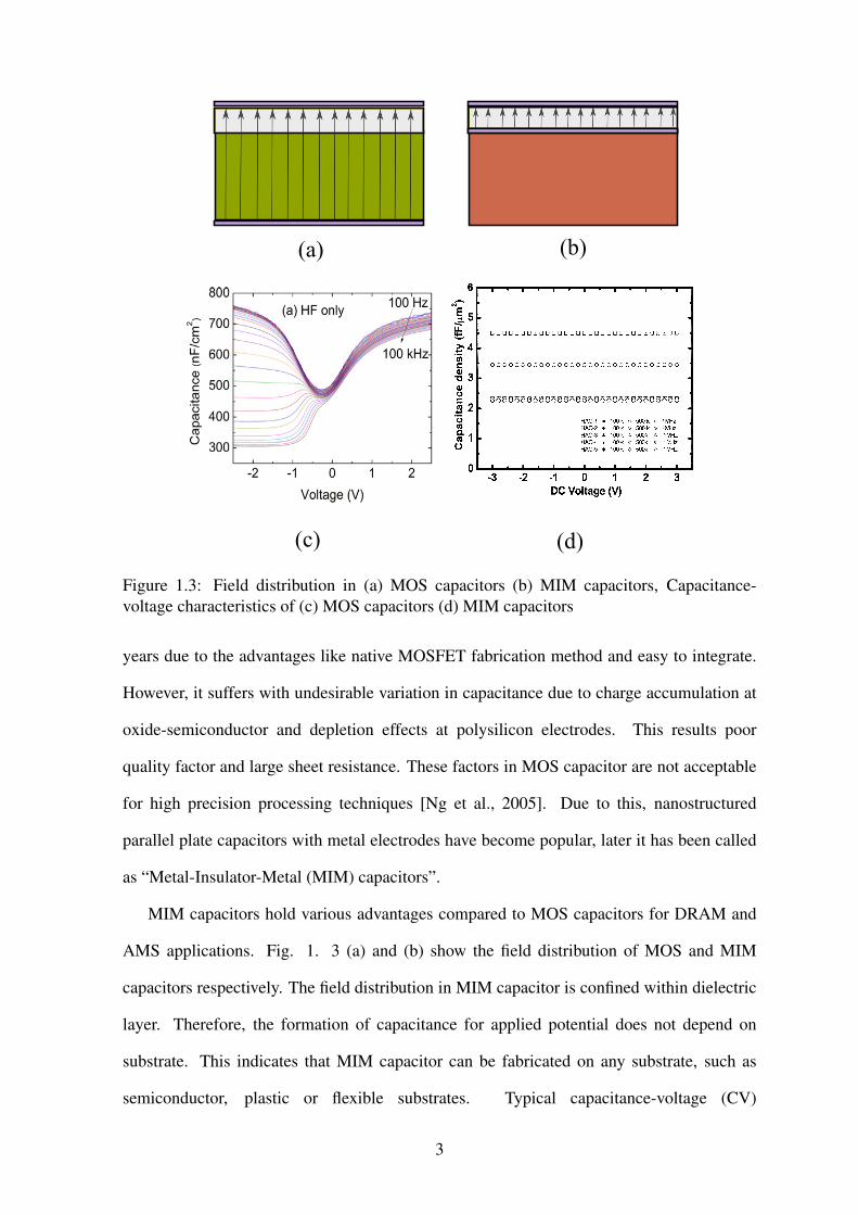
(a) (b)
(c) (d)
Figure 1.3: Field distribution in (a) MOS capacitors (b) MIM capacitors, Capacitance-voltage characteristics of (c) MOS capacitors (d) MIM capacitors
years due to the advantages like native MOSFET fabrication method and easy to integrate.
However, it suffers with undesirable variation in capacitance due to charge accumulation at
oxide-semiconductor and depletion effects at polysilicon electrodes. This results poor
quality factor and large sheet resistance. These factors in MOS capacitor are not acceptable
for high precision processing techniques [Ng et al., 2005]. Due to this, nanostructured
parallel plate capacitors with metal electrodes have become popular, later it has been called
as “Metal-Insulator-Metal (MIM) capacitors”.
MIM capacitors hold various advantages compared to MOS capacitors for DRAM and
AMS applications. Fig. 1. 3 (a) and (b) show the field distribution of MOS and MIM
capacitors respectively. The field distribution in MIM capacitor is confined within dielectric
layer. Therefore, the formation of capacitance for applied potential does not depend on
substrate. This indicates that MIM capacitor can be fabricated on any substrate, such as
semiconductor, plastic or flexible substrates. Typical capacitance-voltage (CV)
3

characteristics of MOS and MIM capacitors are shown in Fig 1. 3 (c) and 1. 3 (d),
respectively. Unlike MOS capacitors, the variation of capacitance due to applied voltage is
very low which is suitable for precision AMS applications [Ng et al., 2005]. International
Technology Roadmap for Semiconductors (ITRS) has predicted the future challenges and
recommendations on MIM capacitors for DRAM and AMS applications [ITRS, 2011]. To
achieve those challenges, many reports have been presented on fabrication of high-k
dielectric MIM capacitors using various dielectric deposition techniques. It is observed that
the performance of MIM capacitors is highly affected by structural defects and polarization
[Gonon and Vallae, 2007].
“Anodization” is acknowledged as a high quality oxidation technique to produce low
defect metal oxide thin films. The ionic polarization is also improved for anodic metal
oxides [Kosjuk and Odynets, 1997]. However, fabrication of nanostructured MIM
capacitors using anodization is rarely reported [Hourdakis and Nassiopoulou, 2010, Sedghi
et al., 2011]. In this thesis, we have presented the fabrication of nanostructured high
performance MIM capacitors using anodization of various high-k dielectric materials, such
as alumina, titania and their bilayer stack. The effect of fabrication process parameters,
such as electrolyte, anodization voltage and temperature, on the structural and electrical
properties of MIM capacitors are studied in detail. This thesis suggests the anodic oxidation
technique for the fabrication of future nanoelectronic ICs for AMS and DRAM
applications.
1.2 Performance parameters of MIM Capacitors
The performance of the MIM capacitor can be evaluated by many parameters, such as
capacitance density, leakage current density, voltage nonlinearity, breakdown field,
dielectric relaxation, dependence of capacitance with frequency and reliability. The
minimum and maximum values of these parameters are limited based on the applications.
For example, the dependence of capacitance with voltage in a MIM capacitor is acceptable
4
in DRAM circuit, but that is severely constrained in analog or mixed signal applications.
However, the leakage current density is limited to almost same as 10nA/cm2 for both the
applications. The leakage current density should be extremely low for blocking capacitors,
but decoupling capacitors can be leaky. In this section, the performance parameters of MIM
capacitors are reviewed with short notes.
1.2.1 Capacitance density
Integrated MIM capacitors are planar parallel plate capacitors. Its capacitance density can
be expressed using the well known equation,
CA=
ε0εr
d(1.2.1)
where C and A are capacitance and electrode area, respectively. ε0, εr and d are free space
dielectric constant, material dielectric constant and thickness of dielectric layer, respectively.
Since all IC designs have scaled to micrometer level, the capacitance density is preferred
with unit of “ f F/µm2”. εr is also represented as k elsewhere. It is clear that the capacitance
density is directly proportional to dielectric constant and inversely proportional to dielectric
thickness. In this regard, many high-k materials have been introduced in MIM capacitors,
whose dielectric constant is higher than that of SiO2 (k = 3.9). On the other hand, thickness
of dielectric layer d should be as lower as possible which depends on dielectric deposition
method and acceptable leakage current density.
High-k dielectric materials such as Al2O3, HfO2, and Ta2O5 have been used in MIM
capacitors which show high capacitance density with good reliability and low leakage
current density [Mondon and Blonkowski, 2003, Lee et al., 2003, Be’cu et al., 2006, Cheng
et al., 2008]. Ferroelectric materials show several orders of dielectric constant than
paraelectrics. BaTiO3, BrxSr1-xTiO3 and other ferroelectric materials have also been
employed recently [Ulrich and Schaper, 2000, Kaynak et al., 2011]. It has been found that
the crystalline properties, grain size, processing temperature are largely affecting the quality
and dielectric constant of materials.
5

Figure 1.4: Voltage linearity characteristics of Al2O3 MIM capacitors.
1.2.2 Voltage linearity
In AMS applications, the each swing of signal (peak-to-peak) is discretized by 1000 or more
levels. In such cases, a small change in capacitance due to temperature or applied voltage
may lead to error in many calculations. This sensitivity to voltage is measured using voltage
coefficient of capacitance (VCC) [Onge et al., 1992],
VCC =
[C(V )−C0
C0
]×106 (ppm/V ) (1.2.2)
where C0 is capacitance measured at zero voltage. For example, Fig. 1. 4 shows the
calculated VCC from measured capacitance-voltage (CV) characteristics of MIM
capacitance with Al2O3 dielectrics [Hourdakis and Nassiopoulou, 2010]. In most of the
cases, the relation of VCC with voltage is parabolic in nature. Such parabolic
characteristics are modeled using the empirical relation,
C(V ) =C0(αV 2 +βV +1
)where α and β are quadratic and linear coefficients of capacitance with units ppm/V 2
and ppm/V respectively. These parameters are extracted by fitting empirical equation with
measured CV data. Quadratic coefficient is positive for many materials and negative for
6

few ferroelectrics & SiO2 [Phung et al., 2011, Kim et al., 2004]. The sign of α depends on
density of induced and permanent dipoles in dielectrics [Phung et al., 2011]. Modeling and
origin of quadratic coefficient are explained in Chapter-6.
For AMS applications, the challenge lies in reducing the VCC value to less than
100ppm/V 2 [ITRS, 2011]. It has been found in many reports that the VCC is largely
depending on polarization, thickness of dielectric layer, atomic arrangement, defect density,
temperature and signal frequency [Phung et al., 2011, Gonon and Vallae, 2007] . Gonon et
al reported the modeling of VCC as a function of frequency and trap density based on
electrode polarization mechanism [Gonon and Vallae, 2007]. It was observed that the
dependence of capacitance in MIM capacitor is due to field activated mobility or hopping of
charges with polarization [Gonon and Vallae, 2007]. The model specifies the VCC as,
4CC0
∝σ2n
0ω2n (1.2.3)
where, 4C is the change in capacitance with voltage and C0 is capacitance at zero bias.
It shows that the VCC decreases with frequency which was confirmed with measured data
[Gonon and Vallae, 2007]. It also indicates that the high conductance dielectrics may get
high VCC which is influenced by defect density in dielectrics.
1.2.3 Frequency dependence
Frequency dependence of capacitance is an useful tool to analyze the polarization,
structural defect profile and dielectric relaxation in dielectrics. When an AC signal is
applied to MIM capacitor, the dipoles of dielectric material orient according to the positive
and negative half cycles. This rotation or polarization with electric field direction is a
mechanical phenomenon which can not follow the high frequency electrical signal. Thus,
the polarization and polarizability of material reduces. This causes reduction in dielectric
constant or capacitance with increase in frequency, such effect is referred as frequency
dependence of capacitance (FDC). The atomic arrangement and defect profile of dielectric
7
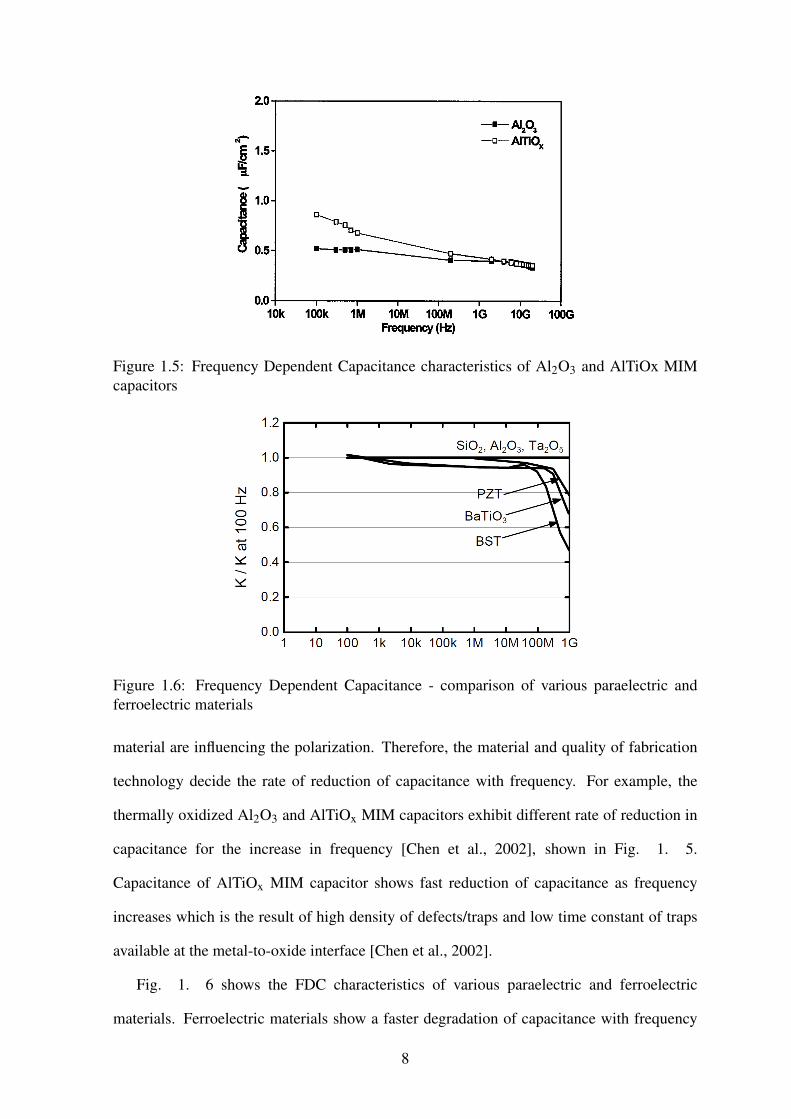
Figure 1.5: Frequency Dependent Capacitance characteristics of Al2O3 and AlTiOx MIMcapacitors
Figure 1.6: Frequency Dependent Capacitance - comparison of various paraelectric andferroelectric materials
material are influencing the polarization. Therefore, the material and quality of fabrication
technology decide the rate of reduction of capacitance with frequency. For example, the
thermally oxidized Al2O3 and AlTiOx MIM capacitors exhibit different rate of reduction in
capacitance for the increase in frequency [Chen et al., 2002], shown in Fig. 1. 5.
Capacitance of AlTiOx MIM capacitor shows fast reduction of capacitance as frequency
increases which is the result of high density of defects/traps and low time constant of traps
available at the metal-to-oxide interface [Chen et al., 2002].
Fig. 1. 6 shows the FDC characteristics of various paraelectric and ferroelectric
materials. Ferroelectric materials show a faster degradation of capacitance with frequency
8

compared to paraelectric materials. This is due to high trap density and grain size of
ferroelectrics which are not suitable for AMS application. However, the ferroelectrics can
show a high dielectric constant even at 1GHz, which can be useful for memory applications.
MIM capacitors should hold a very low dielectric loss and low series resistance. In most
of the fabrication technologies, the metal ions of electrode are migrating into dielectric
layer during very high temperature metalization or oxidation. This intern reduces the
quality and reliability of dielectric material. This needs a low contact resistance
interconnects, desirably short. In recent works, many researchers have shown interests on
copper/low-k dielectric contacts which offers a ultra low series resistance and provides good
integration with silicon/GaAs technologies [M. Armacost and Stein, 2000, C. H. Ng and
Chu, 2002]. These electrodes stop the migration of metal-ions into dielectric layer which
further improve the reliability [C. H. Ng and Chu, 2002]. These low-k contacts also reduces
parasitic capacitance with nearby metal contacts.
1.2.4 Leakage current density
Leakage current density is one of the most important performance parameters of MIM
capacitors. Indeed, the suppression of leakage is one of the most important interest of this
thesis. It is proved, experimentally and mathematically, that the leakage current density is
higher at high-k materials due to low Schottky barrier height and low effective barrier
thickness [Mise et al., 2010].
Four leakage mechanisms in dielectrics are reported so far, namely Schottky emission
(SE), Poole-Frenkel (PF) emission, Trap assisted tunneling (TAT), and Poole-Frenkel
saturation (PFS). Each mechanism dominates other at various range of applied voltage and
trap distribution in dielectrics. Fig. 1. 7 shows the leakage mechanisms in anodic alumina
MIM capacitor. Higher slope at very low voltage indicates the schottky thermionic emission
of electrons to the unoccupied defect or trap states near metal-insulator interface. Low field
current density is dominated by TAT, which depends on temperature, defect density and trap
9

-12
-11
-10
-9
-8
-7
-6
-5
-4
-3
-2
0 3 6 9 12 15 18 21 24
log
(J)
(A
/cm
2)
Applied Voltage (V)
14.3nm
(SE) (TAT)
(PF
T)
(PFS)
(Anodic Al2O3)
Figure 1.7: Various leakage mechanisms in MIM capacitors
Figure 1.8: Schottky emission in metal-insulator interface
well depth. PF emission occurs at high field which is due to the trapped electrons of defect
states are enhanced to conduction states in bulk dielectrics. Poole-Frankel saturation is
observed after the 2nd knee point. Trap barrier height is reduced to zero for voltages above
2nd knee point, thus the charged (Coulombic) traps have no effect on the carrier transport
[Southwick III et al., 2010].
Schottky Emission
The transmission of charge carriers across the metal-insulator barrier for the applied field
is referred as Schottky emission (SE). Fig. 1. 8 shows the conduction band edge of metal-
insulator interface at equilibrium (E = 0) and applied potential (E > 0). At higher applied
electric field, the bending of conduction band takes place which is referred as force induced
10

Figure 1.9: Poole-Frenkel emission in bulk traps
barrier bending [Lenzlinger and Snow, 1969]. The reduction of band edge is given as4φ =
q√
qE4πε
. This activity of electric field leads to thermionic emission of electron from metal
electrode to unoccupied interface traps at insulator. The emission current is generalized from
Richardson-Schottky equation,
JSE =4πm∗
h3 (kBT )2 exp
[−(φ0−βSE
√E)
kBT
](1.2.4)
here, barrier height φ0 = φm−χe with φm maximum barrier height and χe electron affinity
and βSE =√
q4πε
. The activation energy φ0−βSE√
E is largely affected by dielectric constant
of insulator. As dielectric constant increases, the barrier height decrease and the slope of
bending is fastened. This leads to large leakage for high-k dielectrics.
Poole-Frenkel emission
Poole-Frenkel (PF) emission is similar to SE mechanism, both are results of band lowering
for the applied field. While SE is associated with metal-insulator thermionic transition, the
PF is carrier emission from trap to trap at bulk. Fig. 1. 9 show the energy band diagram
of traps, where trap-1 is neutral/positive which is filled with charges. This trap can not take
charges due to coulombic potential by filled states, where as trap-2 can occupy charges.
The conduction band bends for the applied field which makes the energy difference of
4φPF between traps. This energy difference supports the emission of carriers from filled
11
traps to unfilled traps takes place at high applied field. This emission is called PF emission.
This similarity with SE mechanism used to model the4φPF as
4φPF = q
√qEπε
The difference between the SE and PF equation is the denominator 4 inside the square
root. If the trap to trap distance is z, then the distance between trap of metal to trap of
insulator is 2z due to the image effect of metal. This is explained in inset of Fig. 1. 10. With
this, the PF emission can be modeled as,
JPF = qNCexp
[−(φSE −βPF
√E)
kBT
](1.2.5)
where NC is free carrier or trap concentration in insulator and βPF =4φPF/√
E. Since
the thermal energy is largely affecting the energy states of traps, the PF emission is further
enhanced by temperature.
Trap assisted tunneling (TAT)
The inter-trap tunneling is classified into two based on the energy state E of the electron
with respect to trap energy ED, namely TAT and PF emission mechanisms. Trap assisted
tunneling rate is expressed with p number of phonon with energy }ω . According to Ridley
[Ridley, 1978], the rate of tunneling and current density are,
TDD =π
}2ω× exp
[−S(2n+1)− p}ω
2kBT
](1.2.6)
JTAT = AT NtTDDexp [(qV −φ1 +φt)/kBT ] (1.2.7)
here the phonon occupation number is n = [exp([}ω/kBT ])−1]−1 and S is Huang–Rhys
factor [Ridley, 1978]. The 3D TAT is presented by Hartke [Hartke, 1968] which reports
useful approximations in calculation of direct tunneling probability.
12

Figure 1.10: CVS and TBD characteristics of Ta2O5 MIM capacitor
1.2.5 Dielectric relaxation and Dielectric reliability
Dielectric relaxation (DR) in MIM capacitors is one the error source for mixed signal ICs,
particularly it attacks the A/D converters [Ning et al., 2008]. Dielectric relaxation refers the
time dependent trapping and releasing of charges/carriers in defect of dielectrics.
Polarization of the trapped charges occurs during relaxation for the changes in applied
voltage. This leads to time dependent current variations in MIM capacitor. Such mechanism
is also referred as memory effect [Ning et al., 2008]. This time dependent charge transfer
affects the VCC of capacitors and disturbs the AMS system.
Reliability is a statistical information about the device performance under certain
real-time conditions, such as electrical, temperature and mechanical stresses. In MIM
capacitor, the reliability is based on the electrical stress with time, voltage and temperature.
It specifies the life time of MIM capacitor under continues time electrical stress. To
measure this parameter, the leakage current density of test device is measured at an applied
voltage for period of time, say 105 second at 20V . This applied electrical stress creates new
traps in dielectric layer which changes the leakage current, this is called stress induced
leakage current (SILC). The newly created traps form a leaky path which results in
breakdown. The time of breakdown (TBD) can be measured at various high voltages. A
13

typical TBD characteristics of Ta2O5 MIM capacitor is shown in Fig. 1. 10 (b) [Sedghi
et al., 2011]. This capacitor shows a high reliability which shall breakdown after 10 years if
1V is applied continuesly.
1.3 Thesis Motivation and Outline
Motivation of the thesis
MIM capacitors are one of the attractive passive components for analog, mixed signal and
memory applications. However, they take a large area in ICs. International Technology
Roadmap for Semiconductors (ITRS) has already recommended about the miniaturization
of MIM capacitors. High capacitance with small electrode area can be achieved using high
permittivity dielectric materials. ITRS has predicted that MIM capacitors should hold a
high capacitance density of > 5 f F/µm2, low voltage linearity of < 100ppm/V 2 and low
leakage current density of < 10nA/cm2 by the year 2015. In this regard, many works were
carried out over the last decade with various high-k dielectrics. However, many of them are
facing problems with structural defects, interface traps and poor polarization process due to
limitations of fabrication process. From literature review presented in Chapter-2, the primary
qualities required for the dielectric layer of MIM capacitors are listed below:
1. Low defect density
2. Low fabrication temperature
3. Crystalline dielectric layer
4. Good electrical and thermal stability
5. Low fabrication cost
We used anodization technique to fabricate MIM capacitors to meet these requirements.
Anodization is widely accepted as low defect oxidation method which yield high quality
metal oxides. It results two structures, namely porous and barrier type anodic oxides, based
14
on the electrolyte used. It is observed from the literature survey that the barrier type anodic
oxides are having potential to solve these issues. By keeping these observations in mind, the
objectives of the thesis are set. The motivations of this thesis are:
• to fabricate MIM capacitors using anodization technique to achieve a high capacitance
density of > 5 f F/µm2 and low leakage current density of < 10nA/cm2 with low
voltage linearity according to ITRS recommendations.
• to study the polarization and conduction mechanisms involved in the electrical
properties of anodic MIM capacitors
• to model the CV characteristics of high-k MIM capacitors and identify the origin of
nonlinearities.
Thesis Outline
In this thesis, Chapter-2 presents the detailed review on recent fabrication trends of MIM
capacitors. It also presents the requirement and challenges in preparation and
characterization of dielectric materials.
In Chapter-3, the fabrication of alumina MIM capacitors using anodization technique is
discussed in details. It also presents the structural and electrical properties through various
characterization tools. Conduction mechanism, reliability and frequency dependency of
capacitance are reported in detail.
Fabrication of anodic titania MIM capacitors is discussed in detail in Chapter-4. The
anodic titania offers a high performance and high capacitance MIM capacitor. The crystalline
property and nucleation process are discussed in detail with electrical properties.
Chapter 5 presents the fabrication of anodic TiO2/Al2O3 MIM capacitors. It also
specifies the structural and electrical properties in details, such as crystalline, nucleation,
capacitance and leakage characteristics. Effect of electrolyte on the performance of titania
MIM capacitors is studied with structural and electrical properties.
15

Modeling of capacitance-voltage characteristics for single and multilayer MIM
capacitors is presented in Chapter-6. This explains the VCC, FDC characteristics
dependence with voltage and predicts the origin of nonlinearities in formation of
capacitance. A detailed summary of anodic oxides MIM capacitors and conclusions are
made in Chapter 6.
16