channel design, simulation and measurement with the shift from parallel bus interfaces to serial...
TRANSCRIPT
Channel Design, Simulation and
Measurement
GRL Company Confidential

SI Modeling & Simulation
Model Validation Testing &
Refinement
Board Characterization
& Probing
IC Bring-Up, Debug Testing,
& SERDES tuning
Test Equipment Methodology development
Standards Compliance
Testing
Characterization & Stress Testing
GRL’s multi-disciplinary capabilities help
customers adopt high speed interfaces
GRL Company Confidential

Connectivity Standards Covered
GRL Company Confidential
Authorized Test Lab (ATC) ATC Expected in Early 2012
Now Testing
DP 1.2
First ATC
selected by
Intel/Apple
SandForce
Preferred
ATC
HDMI 1.3/1.4 Now Testing
MHL USB 2.0/3.0
Independent Lab Validation
Now Testing
PCIe Gen3
SandForce
Preferred
ATC
Turnkey
DDR2/DDR3
Testing
10G Ethernet
XAUI, SGMII,
XFI,
SDI, 3G-SDI,
HD-SDI,
6G SDI
D-PHY
M-PHY
SRIO
T1/T2/T3
2.1
OBSAI-1/2/3 CPRI-1/2/3/4 3.75 Gbs CEI 6G
LR/SR
OC 12/48
OTU-1

Agenda
Introduction
Challenges at High Speed
Addressing SI in Early Design
S-parameters Basics
Simulations and Measurements
Conclusions

Introduction
With the shift from parallel bus interfaces to serial links, high data
rate signals have not only changed chip designs but also board
designs. The impact of the physical channel on Signal Integrity has
to be taken into consideration at a very early stage of design.
Simulation accuracy heavily depends on model accuracy. The
correlation between simulation and measurement is a key to a
successful design.
This presentation will address the entire simulation flow including
extraction of channel S-parameters, simulation with the extracted S-
parameter model using Agilent’s ADS transient simulator, and
validation of the simulation through measurement.

Problem: The High Speed Challenge
Traditional wide parallel buses are no longer suitable for high speed
designs. Why?
Difficult to maintain comparable skew between the individual parallel-
signal lines
More power consumed by a faster-switching parallel bus
Difficult to route the individual parallel-signal lines

The High Speed Challenge
Serial Links are better for high speed designs. Why?
Ability to move a large amount of data over a differential pair
Reduces the complexity, cost, power and board space
Enables data rates higher than 10Gbps not feasible with parallel links

The High Speed Challenge
At High Speed, things get tricky…
Digital signals must be handled like microwave signals (rise/fall edge in
50ps range)
Less margin for timing errors
Timing errors can violate the digital circuit setup and hold time, as well as
propagation delay time, leading to logic function failures

The High Speed Challenge
At higher speed, Signal Integrity issues become more problematic:
Transmission Line Effects – Losses and reflections in interconnecting
traces including package leads, vias, connectors and impedance
mismatch
Coupling Effects – Cross talk between signal lines or between signal and
clock lines
Ground Bounce Noise – Faster switching times cause higher transient
current in outputs as they discharge load capacitance. As the current
flows through package inductance, it causes ground bounce noise
Power Integrity – DC supply distribution and decoupling, unwanted
signal and clock propagation through power distribution circuit
Electromagnetic Interference (EMI) – External noise ingress, self-
interference and control of radiated emissions

Solution: Address SI at an
Early Stage of Design
The key to accurate simulation early in the design is to properly
understand and model the impact of the physical channel on the signal
as it travels from the transmitter to the receiver.
Effective design simulation follows these basic steps:
1.Model the Physical Channel using S-parameters
2.Simulate the Model (using Agilent’s ADS suite)
3.Validate the Model through Measurements

1. Model the Physical Channel
Using S-parameters
How can we describe linear two-port (and multi-port) networks?
I1 and I2 are current flow in and out of the net work
V1 and V2 are voltages on the input port and output port
a1, b1 and a2, b2 are normalized forward and backward traveling
waves
Two-port
networks
I1 I2
a1
b1
b2
a2
+
V1
-
+
V2
-
What are S-parameters, anyway?

S-parameter Basics
The network can be described as T-parameters and Z-parameters
Transfer matrix (T-parameter)
Impedance matrix (Z-parameter)
V1
I1
A B
C D
V2
I2
V1
V2
Z11 Z12
Z21 Z22
I1
-I2

S-parameter Basics
It can be described as Y-parameters and…
Admittance matrix (Y-parameter)
I1
-I2
Y11 Y12
Y21 Y22
V1
V2

S-parameter Basics
b1
b2
S11 S12
S21 S22
a1
a2
Scattering matrix (S-parameter)

4-port Single-ended S-parameter Matrix
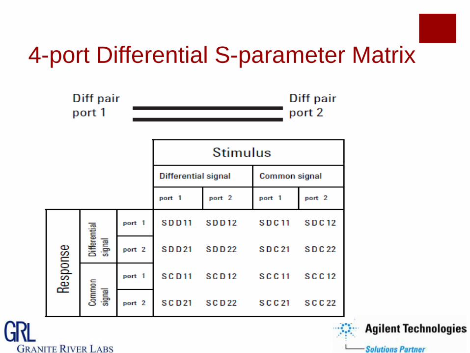
4-port Differential S-parameter Matrix
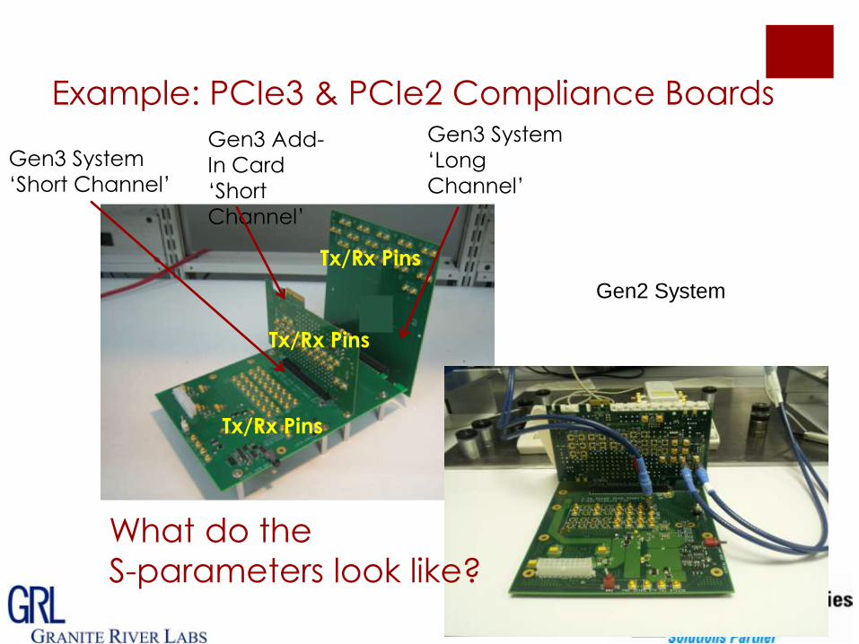
Example: PCIe3 & PCIe2 Compliance Boards Gen3 System
‘Long
Channel’
Gen3 Add-
In Card
‘Short
Channel’
Tx/Rx Pins
Tx/Rx Pins
Tx/Rx Pins
Gen3 System
‘Short Channel’
Gen2 System
What do the
S-parameters look like?

What S-parameters look like…
on a ENA/PNA
SDD21 Insertion Loss SDD11 Return Loss
SDD12 Insertion Loss SDD22 Return Loss

What S-parameters look like…
in Touchstone format

2. Simulate with the Channel
S-parameters in ADS
Create schematics in ADS
Run ADS transient simulation with the measured
channel S-parameters
Simulate eye diagram of the channel
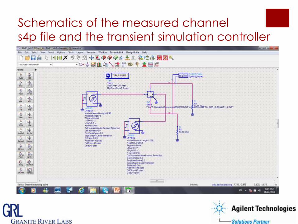
Schematics of the measured channel
s4p file and the transient simulation controller
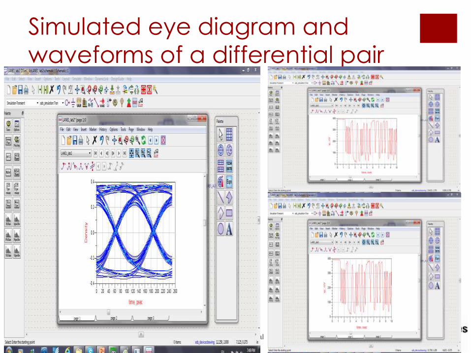
Simulated eye diagram and
waveforms of a differential pair
GRL Company Confidential
19
July
2011
22

3. Verify the Model Through Measurement
Make ‘Embedded Channel’ Measurements using S-parameters

Model Verification Through
Measurement
Make ‘Physical Channel’ Measurements using PCIe Compliance
Load Board/Compliance Base Board (CLB/CBB)
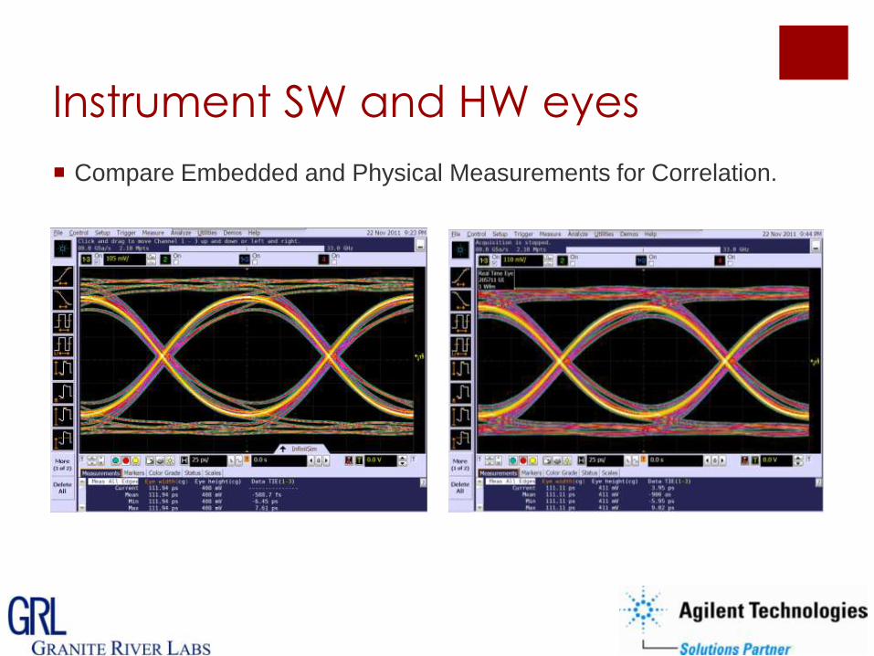
Instrument SW and HW eyes
Compare Embedded and Physical Measurements for Correlation.

PCIe Compliance boards S-parameters
validated by Instrument SW/HW eyes and
ADS simulated eye

Conclusion 1. Approach Board Design and IC Design together
2. Take Signal Integrity issues into consideration early using S-
parameters of the physical channel and media in simulations
3. A basic understanding of S-parameters is key to properly integrate
your Channel Model into your Design
4. Channel Model validation is critical for simulation accuracy
This approach can help you in several ways…
Better timing margin
Avoid re-spin of the design
Get product to market faster and more cost-effectively.
Q&A
THANK YOU!