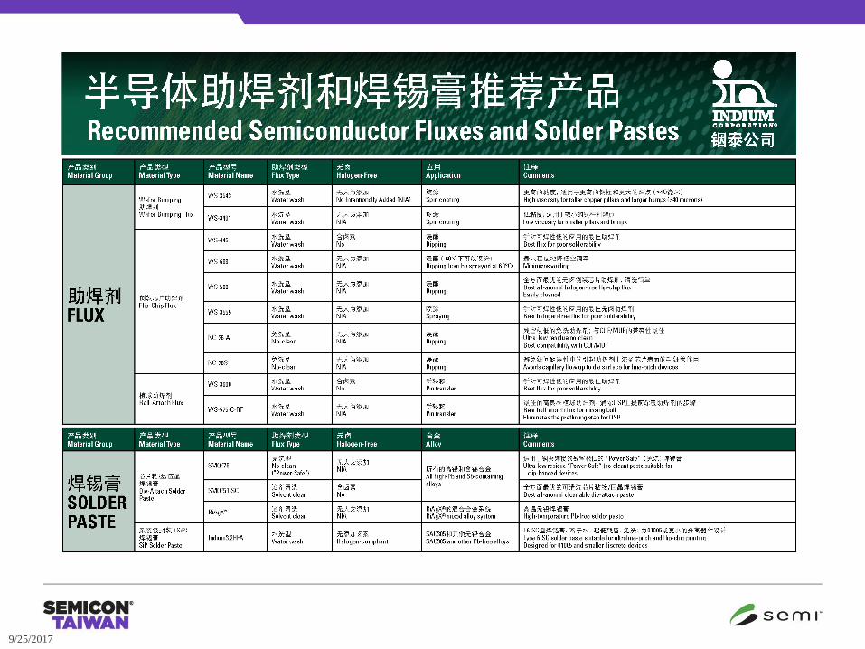
challenges in material applications for sip · 2017-10-03 · •power semiconductor die-attach...
TRANSCRIPT

Challenges in
Material Applications for SiP
Sze PeiLimRegional Product Manager for Semiconductor Products
Indium Corporation

9/25/2017
Indium Corporation
Customer Recognition:
• Intel (Preferred Quality Supplier Award)
• Celestica (Total Cost of Ownership Award)
• Samsung (Superior Vendor Award)
• Shinwa (Best Supplier Awards)
Materials Supplier:
• SMT solder pastes
and fluxes
• Power semiconductor
die-attach
• Semiconductor fluxes
• SiP solder pastes
• TIMs
• Engineered solders
• Specialty compounds
• NanoFoil®

• Introduction
• Challenges
• Solder Paste
• Flip-Chip Flux
• Acknowledgements
• Q & A
Outline/Agenda

• Heterogeneous integration in SiP
– Increased functionality in a single package,
higher performance
– Faster time to market
– Lower cost
• Miniaturization for SiP passives
– Current 01005
– 008004
• (ASE: 2017/2018)
– 0050025
• (2019/2020)
Introduction of SiP

• Solder Paste
– Smaller stencil aperture, tighter gap between pads
– More critical solder paste printing requirements
– Jetting paste?
• Flip-Chip Flux
– Cross contamination of flip-chip flux with solder paste
• Cleaning
– Solder paste and flux cleanability
– Water wash vs. solvent wash
– How clean is clean?
• CUF/MUF
– Flowability
– Compatibility with no-clean flux
9/25/2017
Challenges in Material

Solder Paste: Powder Size
Powder Size (IPC J-STD-005) vs. Minimum Stencil Aperture
• Minimum of 5-6 solder particles across the aperture
• Increase in powder surface area will require more flux or flux with a
better oxidation barrier to protect the powder from surface oxidation
TypeLess than 0.5%
larger than
10% Max.
between
80% Min.
Between
10% Max. Less
than
Minimum
Stencil
Aperture (um)
Approximate
Powder Surface
Area (times)
1 160 150-160 75-150 75 NA NA
2 80 75-80 45-75 45 NA NA
3 60 45-60 25-45 25 270 1.0
4 50 38-50 20-38 20 230 1.2
5 40 25-40 15-25 15 150 1.9
6 25 15-25 5-15 5 90 3.7
7 15 11-15 2-11 2 66 5.6

9/25/2017
High Volume Powder (SAC305)
Type 5 Type 6 Type 6-SG
Type 6-SG Solder Paste Printing
• Water-soluble Indium3.2HF
• 0.1mm aperture
• 50µm-thick stencil

Solder Paste: Flux Types
Standard No-Clean SMT
Paste
Ultralow Residue No-
Clean Water-wash
Typical Flux
Residue (%w/w of
flux) 40-60% 4-10%
Zero after cleaning /
drying
Cleaning Process
Not needed for standard
SMT, but can be solvent-
cleaned Not needed
DI water clean or
aqueous solvent
MUF/CUF
compatibility
Poor if not cleaned
(delamination and
solder bridging)
Usually good if all
solvent removed during
reflow or post-
processing
Excellent if residue
completely cleaned and
dried

• Paste rheology
• Slump behavior
• Stencil life
Solder Paste

Minimum slump or bridging down to 50µm gap
9/25/2017
Printing Performance
125µm x 150µm pad and 50µm gap distance
X (µm) Y (µm) Stencil Thickness (µm)
Area Ratio
150 125 35 0.97
150 112.5 35 0.92
150 100 35 0.86
125 70 35 0.64
125 65 35 0.61
120 60 35 0.57
150 125 50 0.68
150 112.5 50 0.64
150 100 50 0.60
125 70 50 0.45
125 65 50 0.42
120 60 50 0.40

Print down to 0.42 area ratio
9/25/2017
Printing Performance
0.64AR0.62AR0.57AR0.45AR0.42AR0.40AR
1 80
1 60
1 40
1 20
1 00
80
60
40
20
0
Dat
a
Boxplot of Different Aspect Ratio using Paste C
Cpk Cp
0.45AR 2.11 2.33
0.42AR 2.19 2.36
0.40AR 2.03 2.21
0.64AR 2.74 2.91
0.62AR 2.82 3.05
0.57AR 2.42 2.62
Box Plot of Different Aspect Ratios

Powder size comparison T6-SG vs. T7-SG
• T7-SG has smaller standard deviation
Printing Performance
0.40AR T7SG0.40AR T6SG0.42AR T7SG0.42AR T6SG0.45AR T7SG0.45AR T6SG
1 80
1 60
1 40
1 20
1 00
80
60
40
20
0
Data
Boxplot of Volume T6SG vs T7SG

Substrate support system: pallet vs. vacuum
• Vacuum support shows better consistency
Printing Performance
Support Aspect Ratio Cpk Ppk Cp
Pallet 0.68 2.52 1.07 3.20
Pallet 0.64 2.70 1.10 2.97
Pallet 0.60 2.39 1.11 2.61
Vacuum 0.68 2.82 1.29 3.37
Vacuum 0.64 2.91 1.60 3.27
Vacuum 0.60 2.73 1.38 3.19

Next Generation
Water-Soluble Indium3.2HFA SiP Printing Paste
A A
Voiding Performance

Solder Paste for Jetting
• Jetting can dispense dots close to pad and high above the pad
• Faster than dispensing; higher frequency
• Ability to achieve smaller deposits
• Ability to dispense additional paste to increase volume
• Ability to dispense paste in cavity on a substrate

9/25/2017
Jetting Performance

MEMS Lid-Attach
• Consistent rectangles for MEMS
lid-attach with no gaps

Flip-Chip Flux Application Processes

Emerging Flip-Chip Challenges
• Package Design Changes
– Pitch: Shrinking to 100 microns and below
– Die-substrate clearances: Down to 60 microns
and below
– Substrates thin (coreless): Subject to warping
– Logic die: Down to 50 microns thick and
memory (DRAM) down to <20 microns thick
• Flux Cleaning Challenges
– Pitch reduction limits ability to completely
remove water soluble flux residues:
• Corrosive residues left behind
• Block flow of CUF and MUF leading to underfill voiding
• Interfere with CUF and MUF adhesion causing delamination
– Cleaning process:
• Increases substrate warpage after reflow and before underfill
– Die damage
– Cracked solder joints
• Adds costs
Answer:
Move to
no-clean flux

TGA Comparison:
ULR and Standard Residue Fluxes
Standard
reflow peak
maximum

Low-Residue Flux for Mass Reflow
• Flip-Chip Flux NC-26S
• Flip-Chip Flux NC-26-A
• Flip-Chip Flux NC-699
– Different rheology or viscosity is required based on process
and product type
Flip-Chip Flux NC-26S
Flip-Chip Flux NC-26-A
Flip-Chip Flux NC-699
Viscosity (kcsp) 20 4 1.5
Residue Level* 7~8% ~4% <1%
* Residue level was measured by gravimetric method before and after reflow using typical
lead-free SAC profile with convection oven.

ULR Flux:
Importance of Rheology
• High viscosity
– Bridging
– Inability to remove die from tray
• Low viscosity
‒ Flux wicking and
die-surface contamination
‒ Inability to hold die in place
‒ Poor joint strength

Printing Comparison:
TACFlux® 10 and Flip-Chip Flux NC-26S
Flip-Chip Flux NC-26S TACFlux ® 10
40µm-thick
stencil
95mil
(diameter)
175mil
(pitch)
Fluxes were printed on a smooth
copper surface, which makes
slump easier than on a PCB.
12mil diameter
(largest circle)
4mil width
(smallest square)
Fluxes were printed on an ENIG
surface with a solder mask on a
PCB
Parameter setting:
• Kneading: 100 strokes
• Separation: 1mm/sec
• Pressure: 2kg per 8-inch squeegee
Two stencils with different aperture openings:
• Both are 40µm thick
• TACFlux® 10 slumped while Flip-Chip Flux NC-26S did not.
• Flip-Chip Flux NC-26S provided better printing compared to TACFlux® 10

Compatibility with Underfill

Flux and Underfill Materials
Fluxes and Reference Underfill
Low-Residue FluxFlip-Chip Flux NC-026S (NC-26S)
G355
U8410-73C
Flip-Chip Flux NC-026-A (NC- 26-A)
749-17-B (Compatibility Improved Flux)
ReferenceTACFlux 7 (Regular Residue Flux)
Blank (No Flux Applied)

Molded Underfill (G355)
Shear Strength
• G355‐Blank gives best shear strength; next best is 749‐17‐B
• NC-26-A and NC-26S provide similar and proper compatibility
• TACFlux® 7 is worse than others
• After humidity and high temperature (HT) treatment, shear strength
became lower as expected
3500.0
3000.0
2500.0
2000.0
1500.0
1000.0
500.0
0.0G355 G355 with
HTG355 with G355 with G355 with N-26A NC-26-A and 749-17-B
HT
G355 with 749-17-B
and HT
G355 with NC-26S
G355 with G355 with G355 with NC-26S and TACFlux 7 TACFlux 7 and
HT HT
Sh
are
Str
en
gth
(p
si)
G355

Capillary Underfill (U8410-73C)
• 749‐17‐B, NC-26-A, and NC-26S gives similar or even higher shear
strength in some cases than U841073‐Blank (no flux residue)
• U8410‐73C provides good compatibility with no-clean low-residue flux
• TACFlux® 7 is worse than others
• No-clean low-residue fluxes provide good compatibility.
U8410-73C4000.0
3500.0
3000.0
2500.0
2000.0
1500.0
1000.0
500.0
0.0U8410-73C U8410-73C U8410-73C
and HT 749-17- B B and HT and HT TACFlux 7
U8410-73C
with TACFlux 7
and HT
Sh
ea
rS
tre
ng
th (
psi)
U8410-73C U8410-73C U8410-73C U8410-73C U8410-73C U8410-73C
Blank Blank with HT with NC-26-A with NC-26-A with with 749-17- with NC-26S with NC-26S with
Shear Strength

9/25/2017

Flip-chip, MR,
and TCBFlip-chip MR,
and TCB
Flip-chip, TCB
Wafer-bumping
Wafer-bumping
Flux jetting
Reflow and sintering
Vacuum reflow
and sinteringReflow
Cleaning flux and
die-attach paste
Cleaning flux and
die-attach paste
Solder paste
jetting
Solder paste
jetting
Equipment and Materials Partners*

Thank you!