ch03 system buses computer components computer function interconnection structures bus...
Post on 21-Dec-2015
272 views
TRANSCRIPT
CH03 System Buses
• Computer Components• Computer Function• Interconnection Structures• Bus Interconnection• PCI
CH03
TECH Computer Science

Program Concept
• Hardwired systems are inflexible• General purpose hardware can do different tasks,
given correct control signals• Instead of re-wiring, supply a new set of control
signals

What is a program?
• A sequence of steps• For each step, an arithmetic or logical operation, or
data movement is done• For each operation, a different set of control signals is
needed

Function of Control Unit
• For each operation a unique code is provided e.g. ADD, MOVE
• A hardware segment accepts the code and issues the control signals
• We have a computer!

Components
• The Control Unit and the Arithmetic and Logic Unit constitute the Central Processing Unit
• Data and instructions need to get into the system and results out Input/output
• Temporary storage of code and results is neededMain memory

Computer Components:Top Level View

Instruction Cycle
• Two steps:FetchExecute

Fetch Cycle
• Program Counter (PC) holds address of next instruction to fetch
• Processor fetches instruction from memory location pointed to by PC
• Increment PCUnless told otherwise
• Instruction loaded into Instruction Register (IR)• Processor interprets instruction and performs required
actions

Execute Cycle
• Processor-memorydata transfer between CPU and main memory
• Processor I/OData transfer between CPU and I/O module
• Data processingSome arithmetic or logical operation on data
• ControlAlteration of sequence of operations e.g. jump
• Combination of above

Example of Program Execution
Opcode 4bit | Address
Opcode: Intruction
1 = Load AC from memory
2 = Store AC to Memory
5 = Add to AC from memory

Instruction Cycle - State Diagram

Interrupts
• Mechanism by which other modules (e.g. I/O) may interrupt normal sequence of processing
• Program e.g. overflow, division by zero
• Timer Generated by internal processor timer Used in pre-emptive multi-tasking
• I/O from I/O controller
• Hardware failure e.g. memory parity error

Program Flow Control

Program Timing: Short I/O Wait

Program Timing: Long I/O Wait

Interrupt Cycle
• Added to instruction cycle
• Processor checks for interrupt Indicated by an interrupt signal
• If no interrupt, fetch next instruction
• If interrupt pending: Suspend execution of current program Save context Set PC to start address of interrupt handler routine Process interrupt Restore context and continue interrupted program

Instruction Cycle (with Interrupts) - State Diagram

Multiple Interrupts
• Disable interruptsProcessor will ignore further interrupts whilst
processing one interrupt Interrupts remain pending and are checked after first
interrupt has been processed Interrupts handled in sequence as they occur
• Define prioritiesLow priority interrupts can be interrupted by higher
priority interruptsWhen higher priority interrupt has been processed,
processor returns to previous interrupt

Multiple Interrupts - Sequential
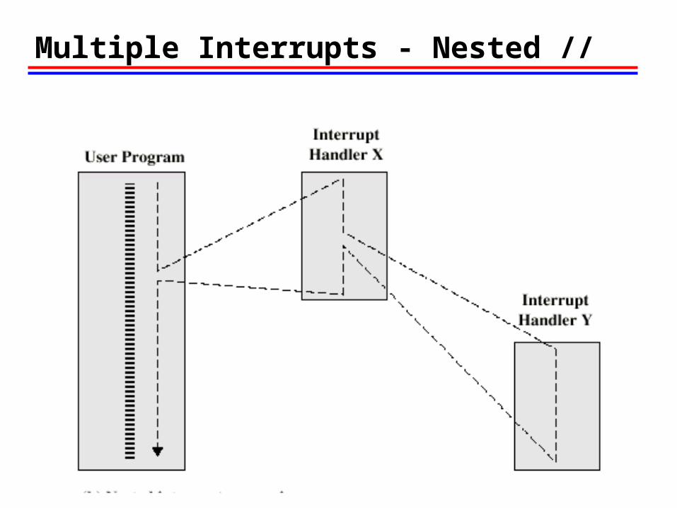
Multiple Interrupts - Nested //

Interconnection Structures: connecting components together
• All the units must be connected• Different type of connection for different type of unit
Memory Input/OutputCPU
Memory Connection
• Receives and sends data• Receives addresses (of locations)• Receives control signals
ReadWriteTiming

Input/Output Connection(1)
• Similar to memory from computer’s viewpoint• Output
Receive data from computerSend data to peripheral
• InputReceive data from peripheralSend data to computer
Input/Output Connection(2)
• Receive control signals from computer• Send control signals to peripherals
e.g. spin disk
• Receive addresses from computer e.g. port number to identify peripheral
• Send interrupt signals (control)

CPU Connection
• Reads instruction and data• Writes out data (after processing)• Sends control signals to other units• Receives (& acts on) interrupts

Buses
• There are a number of possible interconnection systems
• Single and multiple BUS structures are most common• e.g. Control/Address/Data bus (PC)• e.g. Unibus (DEC-PDP)

What is a Bus?
• A communication pathway connecting two or more devices
• Usually broadcast • Often grouped
A number of channels in one bus e.g. 32 bit data bus is 32 separate single bit channels
• Power lines may not be shown

Data Bus
• Carries dataRemember that there is no difference between “data”
and “instruction” at this level
• Width is a key determinant of performance8, 16, 32, 64 bit

Address bus
• Identify the source or destination of data• e.g. CPU needs to read an instruction (data) from a
given location in memory• Bus width determines maximum memory capacity of
system e.g. 8080 has 16 bit address bus giving 64k address
space

Control Bus //
• Control and timing informationMemory read/write signal Interrupt requestClock signals

Bus Interconnection Scheme

Big and Yellow?
• What do buses look like?Parallel lines on circuit boardsRibbon cablesStrip connectors on mother boards
e.g. PCI
Sets of wires

Single Bus Problems
• Lots of devices on one bus leads to:Propagation delays
Long data paths mean that co-ordination of bus use can adversely affect performance
If aggregate data transfer approaches bus capacity
• Most systems use multiple buses to overcome these problems

Traditional (ISA)(with cache)

High Performance Bus //

Bus Types
• DedicatedSeparate data & address lines
• MultiplexedShared linesAddress valid or data valid control lineAdvantage - fewer linesDisadvantages
More complex controlUltimate performance

Bus Arbitration
• More than one module controlling the bus• e.g. CPU and DMA controller• Only one module may control bus at one time• Arbitration may be centralised or distributed

Centralised Arbitration
• Single hardware device controlling bus accessBus ControllerArbiter
• May be part of CPU or separate

Distributed Arbitration
• Each module may claim the bus• Control logic on all modules

Timing
• Co-ordination of events on bus• Synchronous
Events determined by clock signalsControl Bus includes clock lineA single 1-0 is a bus cycleAll devices can read clock lineUsually sync on leading edgeUsually a single cycle for an event

Synchronous Timing Diagram

Asynchronous Timing Diagram
PCI Bus
• Peripheral Component Interconnection• Intel released to public domain• 32 or 64 bit• 50 lines

PCI Bus Lines (required)
• Systems lines Including clock and reset
• Address & Data32 time mux lines for address/data Interrupt & validate lines
• Interface Control• Arbitration
Not sharedDirect connection to PCI bus arbiter
• Error lines

PCI Bus Lines (Optional)
• Interrupt linesNot shared
• Cache support• 64-bit Bus Extension
Additional 32 linesTime multiplexed2 lines to enable devices to agree to use 64-bit transfer
• JTAG/Boundary ScanFor testing procedures

PCI Commands
• Transaction between initiator (master) and target• Master claims bus• Determine type of transaction
e.g. I/O read/write
• Address phase• One or more data phases

PCI Read Timing Diagram

PCI Bus Arbitration

PCI Bus Arbitration (Timing)

Foreground Reading
• Stallings, chapter 3 (all of it)• www.pcguide.com/ref/mbsys/buses/
• In fact, read the whole site!• www.pcguide.com/
Exercises
• Read CH 3• Do Exercise (from handout)• Due BY Email to:
[email protected]• Due by Friday
