ce-ata digital protocol · ce-ata digital protocol revision 1.1 29-september-2005 apple computer,...
TRANSCRIPT

CE-ATA Digital Protocol
Revision 1.1 29-September-2005
Apple Computer, Inc. Hitachi Global Storage Technologies, Inc.
Intel Corporation Marvell Semiconductor, Inc.
Nokia Corporation Seagate Technology LLC
Toshiba America Information Systems, Inc.
ii
This 1.1 revision of the CE-ATA Digital Protocol specification ("Final Specification") is available for download at www.ce-ata.org.
SPECIFICATION DISCLAIMER THIS SPECIFICATION IS PROVIDED TO YOU “AS IS” WITH NO WARRANTIES WHATSOEVER, INCLUDING ANY WARRANTY OF MERCHANTABILITY, NON-INFRINGEMENT, OR FITNESS FOR ANY PARTICULAR PURPOSE. THE AUTHORS OF THIS SPECIFICATION DISCLAIM ALL LIABILITY, INCLUDING LIABILITY FOR INFRINGEMENT OF ANY PROPRIETARY RIGHTS, RELATING TO USE OR IMPLEMNETATION OF INFORMATION IN THIS SPECIFICATION. THE AUTHORS DO NOT WARRANT OR REPRESENT THAT SUCH USE WILL NOT INFRINGE SUCH RIGHTS. THE PROVISION OF THIS SPECIFICATION TO YOU DOES NOT PROVIDE YOU WITH ANY LICENSE, EXPRESS OR IMPLIED, BY ESTOPPEL OR OTHERWISE, TO ANY INTELLECTUAL PROPERTY RIGHTS. Copyright 2004-2005, Apple Computer, Inc., Hitachi Global Storage Technologies, Inc., Intel Corporation, Marvell Semiconductor, Inc., Nokia Corporation, Seagate Technology LLC, Toshiba America Information Systems, Inc. All rights reserved. For more information about CE-ATA, refer to the CE-ATA Workgroup website at www.ce-ata.org.
All product names are trademarks, registered trademarks, or servicemarks of their respective owners. CE-ATA Workgroup Digital Technical Editor:
Amber Huffman Intel Corporation 2111 NE 25th Ave M/S JF2-53 Hillsboro, OR 97124 USA Tel: (503) 264-7929 Email: [email protected]
iii
Table of Contents
1. Introduction ........................................................................................................................... 1 1.1. Goals, Objectives, & Constraints ...................................................................................... 1 1.2. References........................................................................................................................ 1 1.3. Definitions, abbreviations, and conventions...................................................................... 1
1.3.1. Definitions and Abbreviations .................................................................................... 1 1.3.2. Conventions ............................................................................................................... 3 1.3.3. Value representations ................................................................................................ 4
2. Command Protocol ............................................................................................................... 5 2.1. Access Primitives & Protocol ............................................................................................ 5
2.1.1. RW_MULTIPLE_REGISTER (CMD60) ..................................................................... 5 2.1.2. RW_MULTIPLE_BLOCK (CMD61) ........................................................................... 6
2.2. Command Completion Signal ........................................................................................... 7 2.2.1. CMD line state after command completion signal ..................................................... 8 2.2.2. Command Completion Signal Disable ....................................................................... 8
2.3. MMC Data Block Size Negotiation.................................................................................... 9 2.4. Reduced ATA Command Emulation ............................................................................... 10
2.4.1. Reset and Device Discovery.................................................................................... 11 2.4.2. Theory of ATA Command Operation ....................................................................... 12 2.4.3. Device MMC State Machine .................................................................................... 13 2.4.4. Device ATA State Machine Definition...................................................................... 20
3. Timing Requirements.......................................................................................................... 25 3.1. RW_MULTIPLE_REGISTER (CMD60) Timing Diagrams .............................................. 26
3.1.1. Read Timings........................................................................................................... 26 3.1.2. Write Timings ........................................................................................................... 27
3.2. RW_MULTIPLE_BLOCK (CMD61) Timing Diagrams .................................................... 28 3.2.1. Read Single Block Timings...................................................................................... 28 3.2.2. Read Multiple Block Timings ................................................................................... 29 3.2.3. Write Single Block Timings ...................................................................................... 30 3.2.4. Write Multiple Block Timings.................................................................................... 32 3.2.5. Non-Data Timings .................................................................................................... 34 3.2.6. Command Completion Signal Disable for RW_MULTIPLE_BLOCK (CMD61) ....... 35 3.2.7. Command Completion Signal and Command Completion Signal Disable timing requirements........................................................................................................................... 35
4. Reduced ATA Command Set ............................................................................................. 36 4.1. ATA Command Structure ................................................................................................ 36 4.2. Reduced ATA Command Set.......................................................................................... 36
4.2.1. IDENTIFY DEVICE .................................................................................................. 37 4.2.2. READ DMA EXT ...................................................................................................... 40 4.2.3. WRITE DMA EXT .................................................................................................... 43 4.2.4. STANDBY IMMEDIATE........................................................................................... 46 4.2.5. FLUSH CACHE EXT................................................................................................ 48
5. Status and Control Registers.............................................................................................. 51 5.1. Access Primitives ............................................................................................................ 51
5.1.1. Register Read .......................................................................................................... 51 5.1.2. Register Write .......................................................................................................... 52
5.2. Register Definition........................................................................................................... 52 5.2.1. scrTempC Register .................................................................................................. 53 5.2.2. scrTempMaxP Register ........................................................................................... 53 5.2.3. scrTempMinP Register ............................................................................................ 53 5.2.4. scrStatus Register.................................................................................................... 54 5.2.5. scrReAllocsA Register ............................................................................................. 54 5.2.6. scrERetractsA Register............................................................................................ 55 5.2.7. scrCapabilities.......................................................................................................... 55 5.2.8. scrControl................................................................................................................. 55
iv
Appendix A. CE-ATA Command Example ............................................................................... 57 A.1 Overview ......................................................................................................................... 57
A.1.1 ATA Task File Definitions ........................................................................................ 57 A.1.2 MMC Block Timing Diagrams .................................................................................. 57
A.2 READ DMA EXT Example .............................................................................................. 57 A.2.1 ATA Task File .......................................................................................................... 57 A.2.2 READ DMA EXT Command Sequence ................................................................... 58 A.2.3 MMC Bus Transactions............................................................................................ 59
A.3 WRITE DMA EXT Example............................................................................................. 60 A.3.1 ATA Task File .......................................................................................................... 60 A.3.2 WRITE DMA EXT Command Sequence ................................................................. 61 A.3.3 MMC Bus Transactions............................................................................................ 62
1
1. Introduction
1.1. Goals, Objectives, & Constraints This specification defines a physical and logical interface between a storage device and a host. Some of the goals and requirements for the specification include:
• Optimized for handheld embedded applications of storage • Low/minimal pin count • Accommodates fast time-to-market initial solution leveraging existing technologies • Provides interface transfer rates sufficient for current small form factor disk drives with
performance scalability to support several future product generations • Consistent with ATA software infrastructure, but complete legacy software compatibility is
not a requirement • Only a single device need be accommodated per connection
CE-ATA is supported over the MMC electrical interface using a protocol that utilizes the existing MMC access primitives. The interface electrical and signaling definition is as defined in the MMC reference.
1.2. References This specification makes reference to the following specifications: MMC System Specification v 4.0 available to MMCA members under NDA. The CE-ATA specification builds on the MMC specification. Refer to MMCA for IP terms for MMC material. MMC Systems Summary Specification v 3.31 available at http://www.mmca.org/tech/MMC-System-Summary-v3.31.pdf
AT Attachment with Packet Interface – 6 (ATA/ATAPI-6) [INCITS 361:2002]. Published ATA/ATAPI specifications available from ANSI at webstore.ansi.org or from Global Engineering.
1.3. Definitions, abbreviations, and conventions
1.3.1. Definitions and Abbreviations The terminology used in this specification is intended to be self-sufficient and does not rely on overloaded meanings defined in other specifications. Terms with specific meaning not directly clear from the context are clarified in the following sections.
1.3.1.1. ATA (AT Attachment) ATA defines the physical, electrical, transport, and command protocols for the internal attachment of storage devices as defined in the ATA reference.
1.3.1.2. BSY BSY corresponds to bit 7 in the ATA Status register. BSY is set to one to indicate that the device is busy. The ATA BSY signal has no relationship to the MMC Busy signal. Refer to the ATA reference for more information on the BSY bit.
2
1.3.1.3. CE CE is the acronym used for “Consumer Electronics” and commonly refers to consumer and handheld electronic devices.
1.3.1.4. CE-ATA sector size CE-ATA sector size corresponds to the value reported in IDENTIFY DEVICE word 106, refer to Section 4.2.1.4.
1.3.1.5. Data unit The term “data unit” describes 512 bytes of data. All CE-ATA data transfers are an integral multiple of data units.
1.3.1.6. DATx DATx refers to an MMC data line, where ‘x’ signifies a particular data line (0 through 7). An MMC design may support one, four, or eight data lines. See the MMC reference.
1.3.1.7. Dword A Dword is thirty-two (32) bits of data. A Dword may be represented as 32 bits, as two adjacent words, or as four adjacent bytes. When shown as bits the least significant bit is bit 0 and most significant bit is bit 31. The most significant bit is shown on the left. When shown as words the least significant word (lower) is word 0 and the most significant (upper) word is word 1. When shown as bytes the least significant byte is byte 0 and the most significant byte is byte 3. A Dword alignment/granularity means that address/count bits 1-0 are zero.
1.3.1.8. E ‘E’ is used to indicate the end bit of an MMC command. For more details, see Section 3.
1.3.1.9. L ‘L’ is used to indicate a one cycle pull-down on the MMC interface. For more details, see Section 3.
1.3.1.10. MMC data block An MMC data block corresponds to a data transfer on the MMC data lines that includes a start bit, the data to transfer, a 16-bit CRC and the end bit. The size of the MMC data block does not include the start bit, CRC, or the end bit. Refer to Section 2.3 for the allowed MMC data block sizes that may be used with RW_MULTIPLE_BLOCK (CMD61).
1.3.1.11. MMC Busy MMC Busy corresponds to the device asserting MMC data line DAT0 to indicate to the host that the device is not yet ready to receive data on the MMC bus. The MMC Busy signal has no relationship to the ATA BSY signal. Refer to the MMC reference for more information.
1.3.1.12. P ‘P’ is used to indicate a one cycle pull-up on the MMC interface. For more details, see Section 3.
1.3.1.13. S ‘S’ is used to indicate the start bit of an MMC command. For more details, see Section 3.

3
1.3.1.14. word A word is sixteen (16) bits of data. A word may be represented as 16 bits or as two adjacent bytes. When shown as bits the least significant bit is bit 0 and most significant bit is bit 15. The most significant bit is shown on the left. When shown as bytes the least significant byte (lower) byte is byte 0 and the most significant byte (upper) byte is byte 1. The definition of a word in CE-ATA is the same as the definition of a word in ATA. A word alignment/granularity means that address/count bit 0 is zero.
1.3.1.15. Z ‘Z’ is used to indicate a one cycle high impedance state on the MMC interface. For more details, see Section 3.
1.3.2. Conventions The names of abbreviations, ATA commands, fields, and acronyms used as signal names are in all uppercase (e.g., IDENTIFY DEVICE). MMC commands are in uppercase with underscores between words (e.g., RW_MULTIPLE_BLOCK). Fields containing only one bit are usually referred to as the "name" bit instead of the "name" field. Names of device registers begin with a capital letter (e.g., LBA Low register).
1.3.2.1. Precedence If there is a conflict between text, figures, state machines, and tables, the precedence shall be state machines, tables, figures, and then text.
1.3.2.2. Keywords Several keywords are used to differentiate between different levels of requirements.
1.3.2.2.1. mandatory A keyword indicating items to be implemented as defined by this specification.
1.3.2.2.2. may A keyword that indicates flexibility of choice with no implied preference.
1.3.2.2.3. optional A keyword that describes features that are not required by this specification. However, if any optional feature defined by the specification is implemented, the feature shall be implemented in the way defined by the specification.
1.3.2.2.4. reserved A keyword indicating reserved bits, bytes, words, fields, and code values that are set-aside for future standardization. Their use and interpretation may be specified by future extensions to this or other specifications. A reserved bit, byte, word, or field shall be cleared to zero, or in accordance with a future extension to this specification. The recipient shall not check reserved bits, bytes, words, or fields.
4
1.3.2.2.5. shall A keyword indicating a mandatory requirement. Designers are required to implement all such mandatory requirements to ensure interoperability with other products that conform to the specification.
1.3.2.2.6. should A keyword indicating flexibility of choice with a strongly preferred alternative. Equivalent to the phrase “it is recommended”.
1.3.3. Value representations Values that are not immediately followed by a lowercase "b" or "h" are decimal values. Values that are immediately followed by a lowercase "b" (e.g., 01b) are binary values. Values that are immediately followed by a lowercase "h" (e.g., 3Ah) are hexadecimal values.
5
2. Command Protocol
2.1. Access Primitives & Protocol The following sections define the protocol for the access and command primitives. CE-ATA makes use of the following MMC commands:
CMD0 - GO_IDLE_STATE CMD12 - STOP_TRANSMISSION CMD39 - FAST_IO CMD60 - RW_MULTIPLE_REGISTER CMD61 - RW_MULTIPLE_BLOCK The device shall support the MMC commands required to achieve the MMC TRAN state during device initialization. Other interface configuration settings, such as bus width, may require additional MMC commands also be supported. See the MMC reference. GO_IDLE_STATE (CMD0), STOP_TRANSMISSION (CMD12), and FAST_IO (CMD39) are as defined in the MMC reference. RW_MULTIPLE_REGISTER (CMD60) and RW_MULTIPLE_BLOCK (CMD61) are MMC commands defined by CE-ATA. Note that in the figures showing the definitions of MMC commands, the MMC convention is to transmit bit 7 of byte 5 first on the interface.
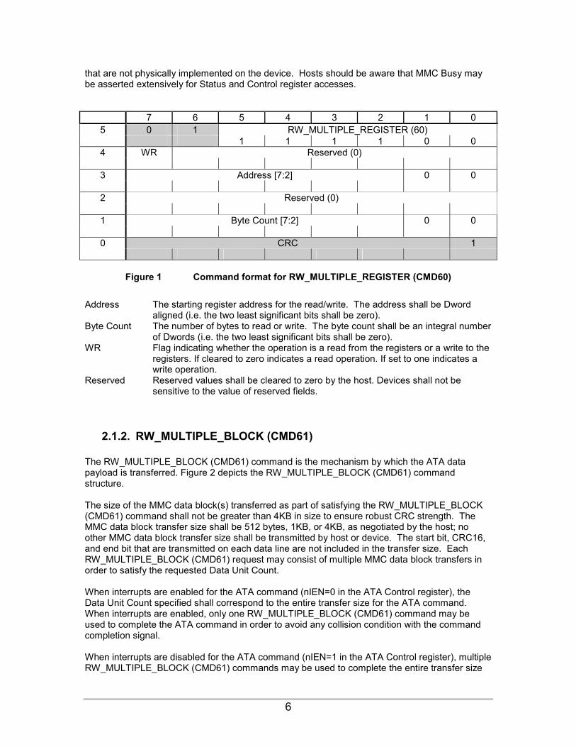
2.1.1. RW_MULTIPLE_REGISTER (CMD60) The RW_MULTIPLE_REGISTER (CMD60) command allows the reading and writing of one or more registers with a single MMC command. Register accesses with this MMC command are always for an integral number of Dwords and have a Dword aligned register address. The RW_MULTIPLE_REGISTER (CMD60) command supports issuing an ATA command by having the complete ATA task file image transmitted in a single MMC command sequence. Figure 1 depicts the RW_MULTIPLE_REGISTER (CMD60) command structure. The host shall not issue a RW_MULTIPLE_REGISTER (CMD60) to an address range outside the task file when there is an ATA command outstanding. The device response to RW_MULTIPLE_REGISTER (CMD60) when parameter WR=0 (R) is R1 as defined in the MMC reference. The device may transmit an MMC data block to the host as defined in Section 2.4. The device response to RW_MULTIPLE_REGISTER (CMD60) when parameter WR=1 (W) is R1b as defined in the MMC reference indicating an optional MMC Busy status to the host. When MMC Busy status is de-asserted, the host may transmit an MMC data block to the device as defined in Section 2.4. Note for RW_MULTIPLE_REGISTER (CMD60) when WR=1 (W): The device should minimize use of MMC Busy on accesses to the taskfile registers such that the host can issue ATA commands efficiently. The device may need to use MMC Busy extensively on access to the Status and Control registers because the Status and Control registers may be virtual registers
6
that are not physically implemented on the device. Hosts should be aware that MMC Busy may be asserted extensively for Status and Control register accesses.
7 6 5 4 3 2 1 00 1 RW_MULTIPLE_REGISTER (60) 5
1 1 1 1 0 0WR Reserved (0) 4
Address [7:2] 0 0 3
Reserved (0) 2
Byte Count [7:2] 0 0 1
CRC 10
Figure 1 Command format for RW_MULTIPLE_REGISTER (CMD60)
Address The starting register address for the read/write. The address shall be Dword
aligned (i.e. the two least significant bits shall be zero). Byte Count The number of bytes to read or write. The byte count shall be an integral number
of Dwords (i.e. the two least significant bits shall be zero). WR Flag indicating whether the operation is a read from the registers or a write to the
registers. If cleared to zero indicates a read operation. If set to one indicates a write operation.
Reserved Reserved values shall be cleared to zero by the host. Devices shall not be sensitive to the value of reserved fields.
2.1.2. RW_MULTIPLE_BLOCK (CMD61) The RW_MULTIPLE_BLOCK (CMD61) command is the mechanism by which the ATA data payload is transferred. Figure 2 depicts the RW_MULTIPLE_BLOCK (CMD61) command structure. The size of the MMC data block(s) transferred as part of satisfying the RW_MULTIPLE_BLOCK (CMD61) command shall not be greater than 4KB in size to ensure robust CRC strength. The MMC data block transfer size shall be 512 bytes, 1KB, or 4KB, as negotiated by the host; no other MMC data block transfer size shall be transmitted by host or device. The start bit, CRC16, and end bit that are transmitted on each data line are not included in the transfer size. Each RW_MULTIPLE_BLOCK (CMD61) request may consist of multiple MMC data block transfers in order to satisfy the requested Data Unit Count. When interrupts are enabled for the ATA command (nIEN=0 in the ATA Control register), the Data Unit Count specified shall correspond to the entire transfer size for the ATA command. When interrupts are enabled, only one RW_MULTIPLE_BLOCK (CMD61) command may be used to complete the ATA command in order to avoid any collision condition with the command completion signal. When interrupts are disabled for the ATA command (nIEN=1 in the ATA Control register), multiple RW_MULTIPLE_BLOCK (CMD61) commands may be used to complete the entire transfer size
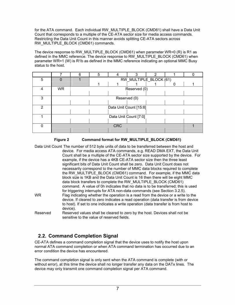
7
for the ATA command. Each individual RW_MULTIPLE_BLOCK (CMD61) shall have a Data Unit Count that corresponds to a multiple of the CE-ATA sector size for media access commands. Restricting the Data Unit Count in this manner avoids splitting CE-ATA sectors across RW_MULTIPLE_BLOCK (CMD61) commands. The device response to RW_MULTIPLE_BLOCK (CMD61) when parameter WR=0 (R) is R1 as defined in the MMC reference. The device response to RW_MULTIPLE_BLOCK (CMD61) when parameter WR=1 (W) is R1b as defined in the MMC reference indicating an optional MMC Busy status to the host.
7 6 5 4 3 2 1 00 1 RW_MULTIPLE_BLOCK (61) 5
1 1 1 1 0 1WR Reserved (0) 4
Reserved (0) 3
Data Unit Count [15:8] 2
Data Unit Count [7:0] 1
CRC 10
Figure 2 Command format for RW_MULTIPLE_BLOCK (CMD61)
Data Unit Count The number of 512 byte units of data to be transferred between the host and device. For media access ATA commands, e.g. READ DMA EXT, the Data Unit Count shall be a multiple of the CE-ATA sector size supported by the device. For example, if the device has a 4KB CE-ATA sector size then the three least significant bits of Data Unit Count shall be zero. Data Unit Count does not necessarily correspond to the number of MMC data blocks required to complete the RW_MULTIPLE_BLOCK (CMD61) command. For example, if the MMC data block size is 1KB and the Data Unit Count is 16 then there will be eight MMC data block transfers to complete the RW_MULTIPLE_BLOCK (CMD61) command. A value of 0h indicates that no data is to be transferred; this is used for triggering interrupts for ATA non-data commands (see Section 3.2.5).
WR Flag indicating whether the operation is a read from the device or a write to the device. If cleared to zero indicates a read operation (data transfer is from device to host). If set to one indicates a write operation (data transfer is from host to device).
Reserved Reserved values shall be cleared to zero by the host. Devices shall not be sensitive to the value of reserved fields.
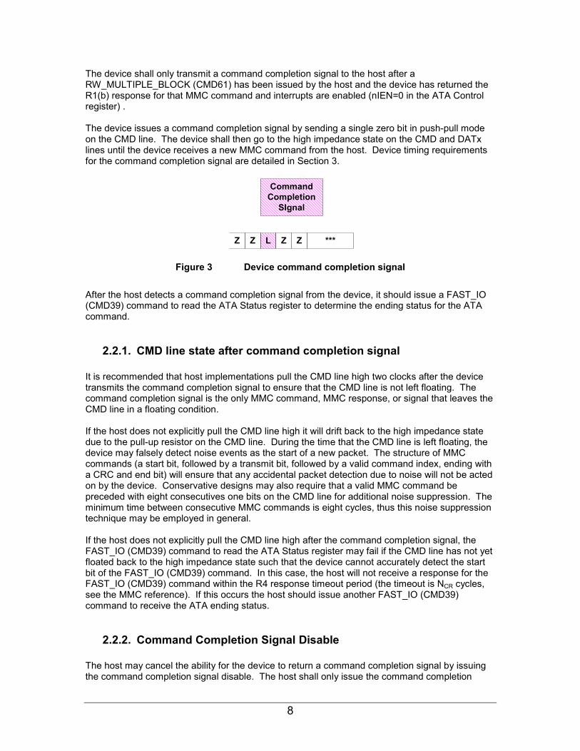
2.2. Command Completion Signal CE-ATA defines a command completion signal that the device uses to notify the host upon normal ATA command completion or when ATA command termination has occurred due to an error condition the device has encountered. The command completion signal is only sent when the ATA command is complete (with or without error), at this time the device shall no longer transfer any data on the DATx lines. The device may only transmit one command completion signal per ATA command.
8
The device shall only transmit a command completion signal to the host after a RW_MULTIPLE_BLOCK (CMD61) has been issued by the host and the device has returned the R1(b) response for that MMC command and interrupts are enabled (nIEN=0 in the ATA Control register) . The device issues a command completion signal by sending a single zero bit in push-pull mode on the CMD line. The device shall then go to the high impedance state on the CMD and DATx lines until the device receives a new MMC command from the host. Device timing requirements for the command completion signal are detailed in Section 3.
Z ***
CommandCompletion
SIgnal
LZ ZZ
Figure 3 Device command completion signal
After the host detects a command completion signal from the device, it should issue a FAST_IO (CMD39) command to read the ATA Status register to determine the ending status for the ATA command.
2.2.1. CMD line state after command completion signal It is recommended that host implementations pull the CMD line high two clocks after the device transmits the command completion signal to ensure that the CMD line is not left floating. The command completion signal is the only MMC command, MMC response, or signal that leaves the CMD line in a floating condition. If the host does not explicitly pull the CMD line high it will drift back to the high impedance state due to the pull-up resistor on the CMD line. During the time that the CMD line is left floating, the device may falsely detect noise events as the start of a new packet. The structure of MMC commands (a start bit, followed by a transmit bit, followed by a valid command index, ending with a CRC and end bit) will ensure that any accidental packet detection due to noise will not be acted on by the device. Conservative designs may also require that a valid MMC command be preceded with eight consecutives one bits on the CMD line for additional noise suppression. The minimum time between consecutive MMC commands is eight cycles, thus this noise suppression technique may be employed in general. If the host does not explicitly pull the CMD line high after the command completion signal, the FAST_IO (CMD39) command to read the ATA Status register may fail if the CMD line has not yet floated back to the high impedance state such that the device cannot accurately detect the start bit of the FAST_IO (CMD39) command. In this case, the host will not receive a response for the FAST_IO (CMD39) command within the R4 response timeout period (the timeout is NCR cycles, see the MMC reference). If this occurs the host should issue another FAST_IO (CMD39) command to receive the ATA ending status.
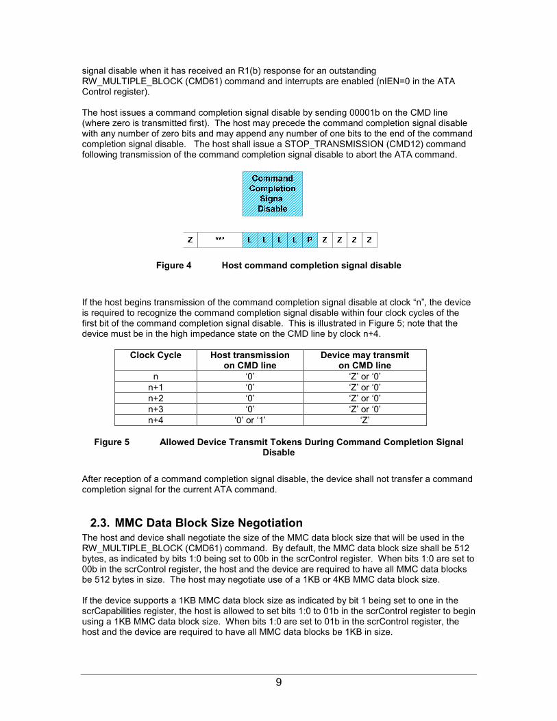
2.2.2. Command Completion Signal Disable The host may cancel the ability for the device to return a command completion signal by issuing the command completion signal disable. The host shall only issue the command completion
9
signal disable when it has received an R1(b) response for an outstanding RW_MULTIPLE_BLOCK (CMD61) command and interrupts are enabled (nIEN=0 in the ATA Control register). The host issues a command completion signal disable by sending 00001b on the CMD line (where zero is transmitted first). The host may precede the command completion signal disable with any number of zero bits and may append any number of one bits to the end of the command completion signal disable. The host shall issue a STOP_TRANSMISSION (CMD12) command following transmission of the command completion signal disable to abort the ATA command.
Figure 4 Host command completion signal disable
If the host begins transmission of the command completion signal disable at clock “n”, the device is required to recognize the command completion signal disable within four clock cycles of the first bit of the command completion signal disable. This is illustrated in Figure 5; note that the device must be in the high impedance state on the CMD line by clock n+4.
Clock Cycle Host transmission on CMD line
Device may transmit on CMD line
n ‘0’ ‘Z’ or ‘0’ n+1 ‘0’ ‘Z’ or ‘0’ n+2 ‘0’ ‘Z’ or ‘0’ n+3 ‘0’ ‘Z’ or ‘0’ n+4 ‘0’ or ‘1’ ‘Z’
Figure 5 Allowed Device Transmit Tokens During Command Completion Signal Disable
After reception of a command completion signal disable, the device shall not transfer a command completion signal for the current ATA command.
2.3. MMC Data Block Size Negotiation The host and device shall negotiate the size of the MMC data block size that will be used in the RW_MULTIPLE_BLOCK (CMD61) command. By default, the MMC data block size shall be 512 bytes, as indicated by bits 1:0 being set to 00b in the scrControl register. When bits 1:0 are set to 00b in the scrControl register, the host and the device are required to have all MMC data blocks be 512 bytes in size. The host may negotiate use of a 1KB or 4KB MMC data block size. If the device supports a 1KB MMC data block size as indicated by bit 1 being set to one in the scrCapabilities register, the host is allowed to set bits 1:0 to 01b in the scrControl register to begin using a 1KB MMC data block size. When bits 1:0 are set to 01b in the scrControl register, the host and the device are required to have all MMC data blocks be 1KB in size.
10
If the device supports a 4KB MMC data block size as indicated by bit 2 being set to one in the scrCapabilities register, the host is allowed to set bits 1:0 to 10b in the scrControl register to begin using a 4KB MMC data block size. When bits 1:0 are set to 10b in the scrControl register, the host and the device are required to have all MMC data blocks be 4KB in size. Refer to Section 5.2 for the definitions of the scrCapabilities and scrControl registers.
2.4. Reduced ATA Command Emulation The Reduced ATA Command set provides a streamlined set of disk commands similar to a subset of the ATA command set. CE-ATA uses a single data transfer mode, DMA. The various transfer mode controls defined in the ATA reference do not apply. The RW_MULTIPLE_REGISTER (CMD60) command is used to write an ATA command packet to a set of registers (often referred to as the task file) at a specific address within the device’s register space. Similarly, ATA command status is retrieved by utilizing the RW_MULTIPLE_REGISTER (CMD60) or FAST_IO (CMD39) commands to read a set of registers at a specific address within the device’s register space. The form and definition of the RW_MULTIPLE_REGISTER (CMD60) command is defined in Section 2.1.1. Figure 6 depicts the mapping of the ATA registers to the MMC register space. The ATA Data register is not mapped because the ATA PIO data transfer protocol is not supported. The Alternate Status register is not mapped because interrupts are not cleared by a Status register read.
Register Address ATA Register (8-bit) 0 Reserved 1 Features (exp) 2 Sector Count (exp) 3 LBA Low (exp) 4 LBA Mid (exp) 5 LBA High (exp) 6 Control 7 Reserved
8 Reserved 9 Features (write) / Error (read) 10 Sector Count 11 LBA Low 12 LBA Mid 13 LBA High 14 Device/Head 15 Command (write) / Status (read)
Figure 6 ATA task file register mapping in MMC register space
Any underlying MMC error that is known to the device will cause an outstanding ATA command to be aborted; the host should retry the entire ATA command. The ATA Status register will have the ERR bit set to one and an appropriate error code will be set in the ATA Error register. If an MMC transport layer error occurs when an ATA command has not yet been successfully issued to the device, the MMC error will not be recorded in the ATA Status or Error registers. On read operations, the device is not aware of any CRC errors that may occur during the data transfer. The host is responsible for checking the host’s MMC status register to determine if any MMC layer error has occurred. If an MMC layer error has occurred during execution of an ATA command, the host shall complete the ATA command with error status.
11
A read of the ATA Control register shall return the last value written. The high-order bit (HOB) defined in the ATA reference in the ATA Control register is reserved in CE-ATA. The host shall not set the HOB bit to one; if HOB is set to one then the device behavior is indeterminate. When interrupts are disabled (nIEN=1 in the ATA Control register), the host should poll prior to each RW_MULTIPLE_BLOCK (CMD61) issued to determine whether an error condition has occurred. It is recommended that the host poll until the BSY bit is de-asserted in the ATA Status register. If BSY=0 and DRQ=1 in the ATA Status register then the host should issue the RW_MULTIPLE_BLOCK (CMD61) command. If BSY=0 and ERR=1 then the ATA command has completed with error and the host should use FAST_IO (CMD39) to determine the cause of the error.
2.4.1. Reset and Device Discovery The underlying MMC reset and initialization procedure for establishing communications between the host and the device is not reproduced here and is as defined in the MMC reference. After completing the normal MMC reset and initialization procedures, the host should query EXT_CSD register byte 504 (S_CMD_SET) in MMC register space. If the ATA bit (bit 4) is set to one then the MMC device is an ATA device. If the device indicates that it is an ATA device, the host should set the ATA bit (bit 4) of the EXT_CSD register byte 191 (CMD_SET) to activate the ATA command set for use. The host selects the command set using the SWITCH (CMD6) command. Host implementations should be aware that CE-ATA devices compliant with the CE-ATA 1.0 specification may not support the ATA mode bits in the EXT_CSD register as the material was developed subsequent to the 1.0 specification. Reception of the GO_IDLE_STATE (CMD0) command shall reset the MMC layer as defined in the MMC reference and shall perform a hard reset to the ATA layer as defined in the ATA reference. When this MMC command is received, there is no requirement for the device to maintain data coherency. After a GO_IDLE_STATE (CMD0), the MMC TRAN state will need to be negotiated to and MMC layer settings will need to be re-initialized. An ATA software reset is performed by issuing two FAST_IO (CMD39) commands back-to-back to the ATA Control register. The first FAST_IO (CMD39) command shall have the SRST bit set to one. The second FAST_IO (CMD39) command shall have the SRST bit cleared to zero. The host shall not set the SRST bit in the ATA Control register to one using RW_MULTIPLE_REGISTER (CMD60). An ATA software reset shall have no effect on the MMC layer. There is no timing requirement between the setting and clearing of the SRST bit in the ATA Control register. The host determines the presence of a CE-ATA device by issuing FAST_IO (CMD39) commands or the RW_MULTIPLE_REGISTER (CMD60) command as defined in Section 2.1.1 after the interface has entered the MMC TRAN state in order to read the present contents of the task file registers. In the presence of a CE-ATA device, the FAST_IO (CMD39) and RW_MULTIPLE_REGISTER (CMD60) commands will succeed and the returned data will be the CE-ATA reset signature as defined in Figure 7. Upon power-on reset, reception of the MMC command GO_IDLE_STATE (CMD0), or ATA software reset, CE-ATA devices shall initialize the task file registers to the values indicated in Figure 7. Note that upon reset or power-on, CE-ATA devices shall set the nIEN bit in the Control register to one.
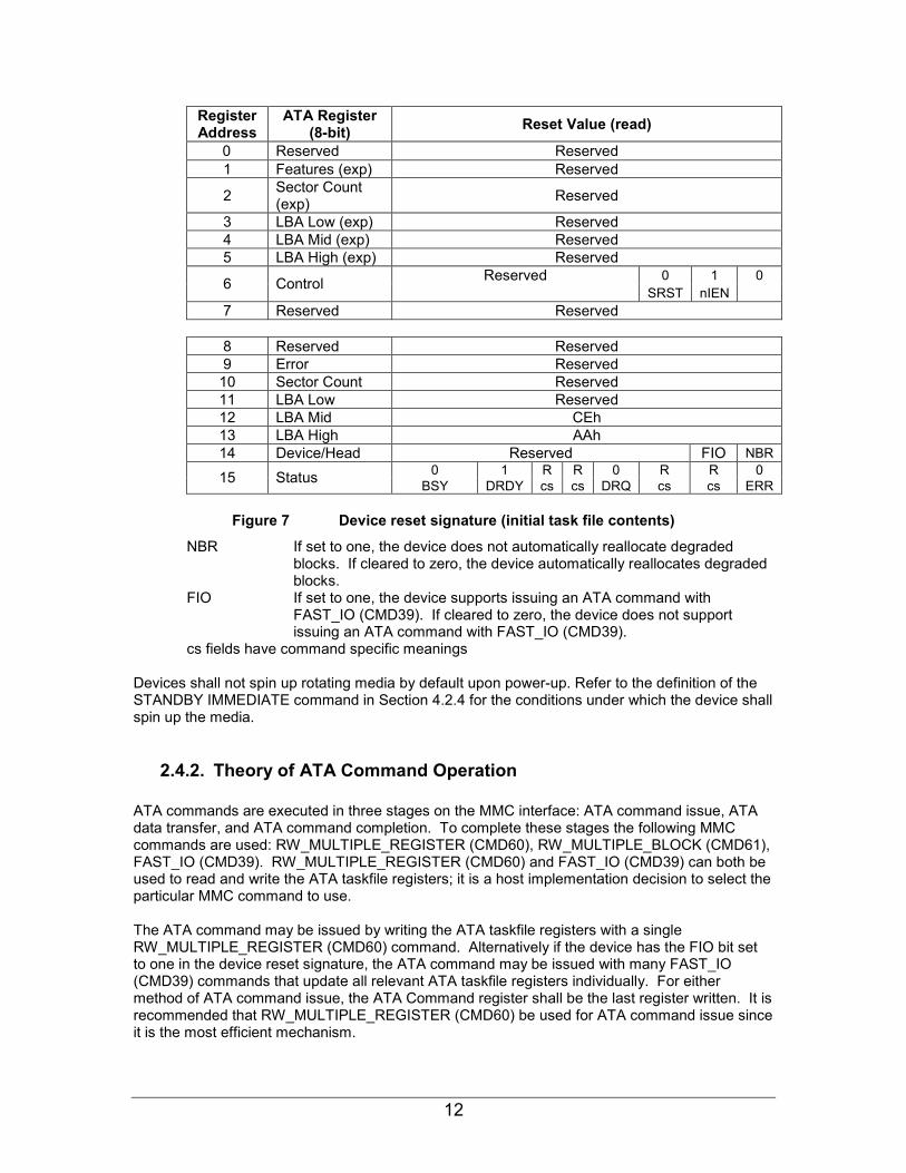
12
Register Address
ATA Register (8-bit) Reset Value (read)
0 Reserved Reserved 1 Features (exp) Reserved
2 Sector Count (exp) Reserved
3 LBA Low (exp) Reserved 4 LBA Mid (exp) Reserved 5 LBA High (exp) Reserved
Reserved 0 1 06 Control SRST nIEN 7 Reserved Reserved
8 Reserved Reserved 9 Error Reserved 10 Sector Count Reserved 11 LBA Low Reserved 12 LBA Mid CEh 13 LBA High AAh 14 Device/Head Reserved FIO NBR
0 1 R R 0 R R 015 Status BSY DRDY cs cs DRQ cs cs ERR
Figure 7 Device reset signature (initial task file contents)
NBR If set to one, the device does not automatically reallocate degraded blocks. If cleared to zero, the device automatically reallocates degraded blocks.
FIO If set to one, the device supports issuing an ATA command with FAST_IO (CMD39). If cleared to zero, the device does not support issuing an ATA command with FAST_IO (CMD39).
cs fields have command specific meanings Devices shall not spin up rotating media by default upon power-up. Refer to the definition of the STANDBY IMMEDIATE command in Section 4.2.4 for the conditions under which the device shall spin up the media.
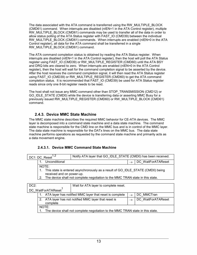
2.4.2. Theory of ATA Command Operation ATA commands are executed in three stages on the MMC interface: ATA command issue, ATA data transfer, and ATA command completion. To complete these stages the following MMC commands are used: RW_MULTIPLE_REGISTER (CMD60), RW_MULTIPLE_BLOCK (CMD61), FAST_IO (CMD39). RW_MULTIPLE_REGISTER (CMD60) and FAST_IO (CMD39) can both be used to read and write the ATA taskfile registers; it is a host implementation decision to select the particular MMC command to use. The ATA command may be issued by writing the ATA taskfile registers with a single RW_MULTIPLE_REGISTER (CMD60) command. Alternatively if the device has the FIO bit set to one in the device reset signature, the ATA command may be issued with many FAST_IO (CMD39) commands that update all relevant ATA taskfile registers individually. For either method of ATA command issue, the ATA Command register shall be the last register written. It is recommended that RW_MULTIPLE_REGISTER (CMD60) be used for ATA command issue since it is the most efficient mechanism.
13
The data associated with the ATA command is transferred using the RW_MULTIPLE_BLOCK (CMD61) command. When interrupts are disabled (nIEN=1 in the ATA Control register), multiple RW_MULTIPLE_BLOCK (CMD61) commands may be used to transfer all of the data in order to allow status polling of the ATA Status register with FAST_IO (CMD39) between the individual RW_MULTIPLE_BLOCK (CMD61) commands. When interrupts are enabled (nIEN=0 in the ATA Control register), all data for the ATA command shall be transferred in a single RW_MULTIPLE_BLOCK (CMD61) command. The ATA command completion status is obtained by reading the ATA Status register. When interrupts are disabled (nIEN=1 in the ATA Control register), then the host will poll the ATA Status register using FAST_IO (CMD39) or RW_MULTIPLE_REGISTER (CMD60) until the ATA BSY and DRQ bits are cleared to zero. When interrupts are enabled (nIEN=0 in the ATA Control register), then the host will wait for the command completion signal to be asserted by the device. After the host receives the command completion signal, it will then read the ATA Status register using FAST_IO (CMD39) or RW_MULTIPLE_REGISTER (CMD60) to get the ATA command completion status. It is recommended that FAST_IO (CMD39) be used for ATA Status register reads since only one 8-bit register needs to be read. The host shall not issue any MMC command other than STOP_TRANSMISSION (CMD12) or GO_IDLE_STATE (CMD0) while the device is transferring data or asserting MMC Busy for a previously issued RW_MULTIPLE_REGISTER (CMD60) or RW_MULTIPLE_BLOCK (CMD61) command.
2.4.3. Device MMC State Machine The MMC state machine describes the required MMC behavior for CE-ATA devices. The MMC layer is decomposed into a command state machine and a data state machine. The command state machine is responsible for the CMD line on the MMC bus and is in control of the MMC layer. The data state machine is responsible for the DATx lines on the MMC bus. The data state machine performs operations as requested by the command state machine and primarily acts as a data movement engine.
2.4.3.1. Device MMC Command State Machine DC1: DC_Reset1,2 Notify ATA layer that GO_IDLE_STATE (CMD0) has been received.
1. Unconditional → DC_WaitForATAReset NOTE: 1. This state is entered asynchronously as a result of GO_IDLE_STATE (CMD0) being
received and on power-up. 2. The device shall not complete negotiation to the MMC TRAN state in this state.
DC2: DC_WaitForATAReset1
Wait for ATA layer to complete reset.
1. ATA layer has notified MMC layer that reset is complete → DC_MMCTran 2. ATA layer has not notified MMC layer that reset is
complete → DC_WaitForATAReset
NOTE: 1. The device shall not complete negotiation to the MMC TRAN state in this state.
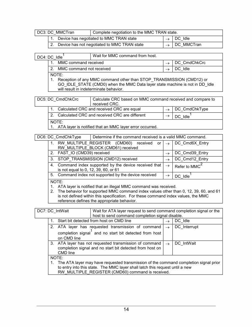
14
DC3: DC_MMCTran Complete negotiation to the MMC TRAN state.
1. Device has negotiated to MMC TRAN state → DC_Idle 2. Device has not negotiated to MMC TRAN state → DC_MMCTran
DC4: DC_Idle1 Wait for MMC command from host.
1. MMC command received → DC_CmdChkCrc 2. MMC command not received → DC_Idle NOTE: 1. Reception of any MMC command other than STOP_TRANSMISSION (CMD12) or
GO_IDLE_STATE (CMD0) when the MMC Data layer state machine is not in DD_Idle will result in indeterminate behavior.
DC5: DC_CmdChkCrc Calculate CRC based on MMC command received and compare to received CRC.
1. Calculated CRC and received CRC are equal → DC_CmdChkType 2. Calculated CRC and received CRC are different → DC_Idle1
NOTE: 1. ATA layer is notified that an MMC layer error occurred.
DC6: DC_CmdChkType Determine if the command received is a valid MMC command. 1. RW_MULTIPLE_REGISTER (CMD60) received or
RW_MULTIPLE_BLOCK (CMD61) received → DC_Cmd6X_Entry
2. FAST_IO (CMD39) received → DC_Cmd39_Entry 3. STOP_TRANSMISSION (CMD12) received → DC_Cmd12_Entry 4. Command index supported by the device received that
is not equal to 0, 12, 39, 60, or 61 → Refer to MMC2
5. Command index not supported by the device received → DC_Idle1
NOTE: 1. ATA layer is notified that an illegal MMC command was received. 2. The behavior for supported MMC command index values other than 0, 12, 39, 60, and 61
is not defined within this specification. For these command index values, the MMC reference defines the appropriate behavior.
DC7: DC_IntWait Wait for ATA layer request to send command completion signal or the host to send command completion signal disable.
1. Start bit detected from host on CMD line → DC_Idle 2. ATA layer has requested transmission of command
completion signal1 and no start bit detected from host on CMD line
→ DC_Interrupt
3. ATA layer has not requested transmission of command completion signal and no start bit detected from host on CMD line
→ DC_IntWait
NOTE: 1. The ATA layer may have requested transmission of the command completion signal prior
to entry into this state. The MMC layer shall latch this request until a new RW_MULTIPLE_REGISTER (CMD60) command is received.
15
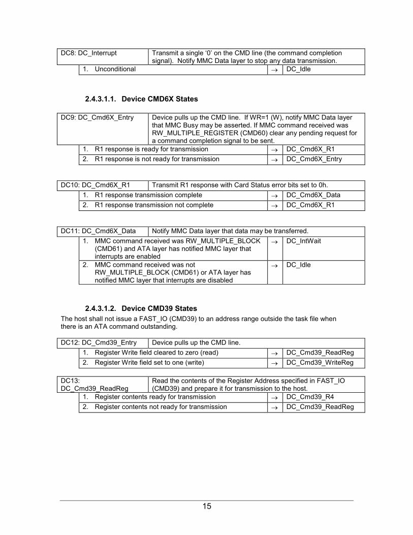
DC8: DC_Interrupt Transmit a single ‘0’ on the CMD line (the command completion signal). Notify MMC Data layer to stop any data transmission.
1. Unconditional → DC_Idle
2.4.3.1.1. Device CMD6X States DC9: DC_Cmd6X_Entry Device pulls up the CMD line. If WR=1 (W), notify MMC Data layer
that MMC Busy may be asserted. If MMC command received was RW_MULTIPLE_REGISTER (CMD60) clear any pending request for a command completion signal to be sent.
1. R1 response is ready for transmission → DC_Cmd6X_R1 2. R1 response is not ready for transmission → DC_Cmd6X_Entry
DC10: DC_Cmd6X_R1 Transmit R1 response with Card Status error bits set to 0h. 1. R1 response transmission complete → DC_Cmd6X_Data 2. R1 response transmission not complete → DC_Cmd6X_R1
DC11: DC_Cmd6X_Data Notify MMC Data layer that data may be transferred. 1. MMC command received was RW_MULTIPLE_BLOCK
(CMD61) and ATA layer has notified MMC layer that interrupts are enabled
→ DC_IntWait
2. MMC command received was not RW_MULTIPLE_BLOCK (CMD61) or ATA layer has notified MMC layer that interrupts are disabled
→ DC_Idle
2.4.3.1.2. Device CMD39 States The host shall not issue a FAST_IO (CMD39) to an address range outside the task file when there is an ATA command outstanding. DC12: DC_Cmd39_Entry Device pulls up the CMD line.
1. Register Write field cleared to zero (read) → DC_Cmd39_ReadReg 2. Register Write field set to one (write) → DC_Cmd39_WriteReg
DC13: DC_Cmd39_ReadReg
Read the contents of the Register Address specified in FAST_IO (CMD39) and prepare it for transmission to the host.
1. Register contents ready for transmission → DC_Cmd39_R4 2. Register contents not ready for transmission → DC_Cmd39_ReadReg
16
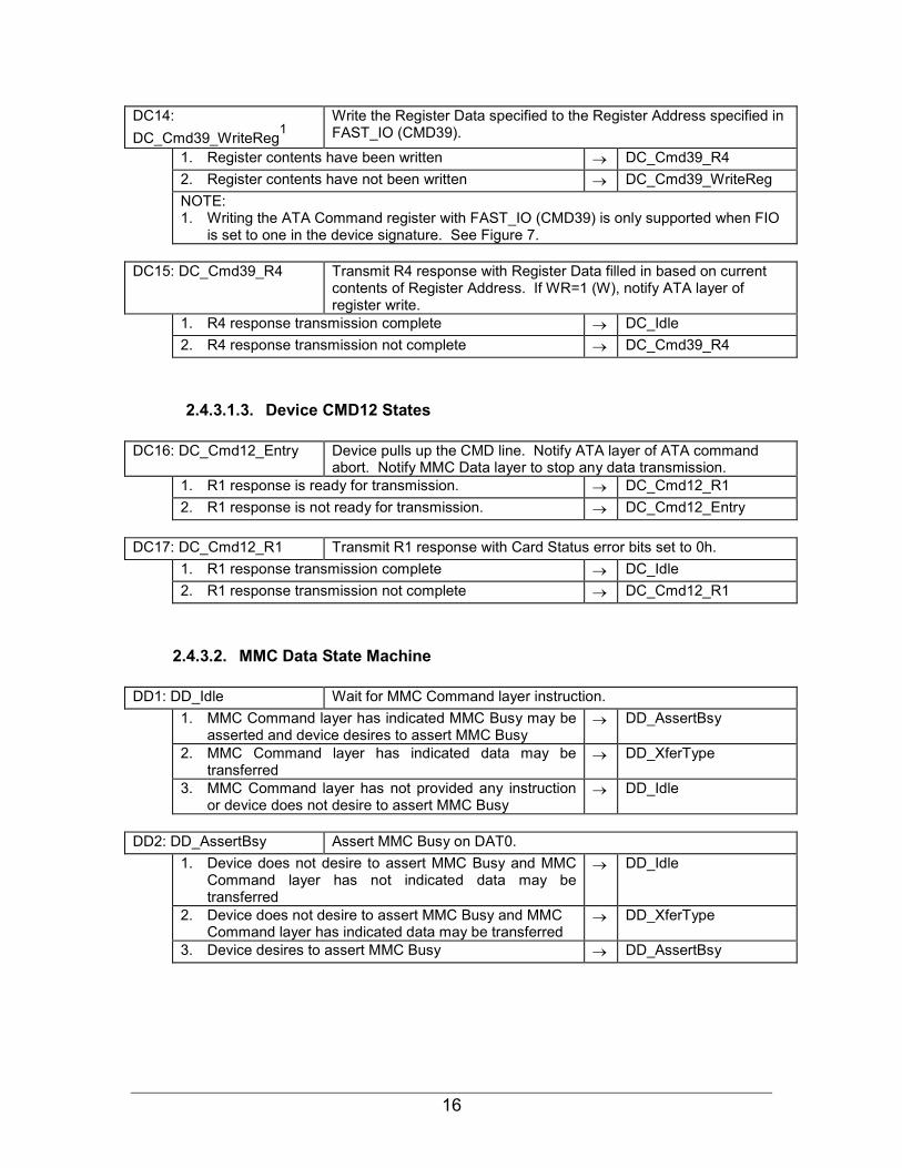
DC14: DC_Cmd39_WriteReg1
Write the Register Data specified to the Register Address specified in FAST_IO (CMD39).
1. Register contents have been written → DC_Cmd39_R4 2. Register contents have not been written → DC_Cmd39_WriteReg NOTE: 1. Writing the ATA Command register with FAST_IO (CMD39) is only supported when FIO
is set to one in the device signature. See Figure 7.
DC15: DC_Cmd39_R4 Transmit R4 response with Register Data filled in based on current contents of Register Address. If WR=1 (W), notify ATA layer of register write.
1. R4 response transmission complete → DC_Idle 2. R4 response transmission not complete → DC_Cmd39_R4
2.4.3.1.3. Device CMD12 States DC16: DC_Cmd12_Entry Device pulls up the CMD line. Notify ATA layer of ATA command
abort. Notify MMC Data layer to stop any data transmission. 1. R1 response is ready for transmission. → DC_Cmd12_R1 2. R1 response is not ready for transmission. → DC_Cmd12_Entry
DC17: DC_Cmd12_R1 Transmit R1 response with Card Status error bits set to 0h. 1. R1 response transmission complete → DC_Idle 2. R1 response transmission not complete → DC_Cmd12_R1
2.4.3.2. MMC Data State Machine DD1: DD_Idle Wait for MMC Command layer instruction.
1. MMC Command layer has indicated MMC Busy may be asserted and device desires to assert MMC Busy
→ DD_AssertBsy
2. MMC Command layer has indicated data may be transferred
→ DD_XferType
3. MMC Command layer has not provided any instruction or device does not desire to assert MMC Busy
→ DD_Idle
DD2: DD_AssertBsy Assert MMC Busy on DAT0.
1. Device does not desire to assert MMC Busy and MMC Command layer has not indicated data may be transferred
→ DD_Idle
2. Device does not desire to assert MMC Busy and MMC Command layer has indicated data may be transferred
→ DD_XferType
3. Device desires to assert MMC Busy → DD_AssertBsy
17
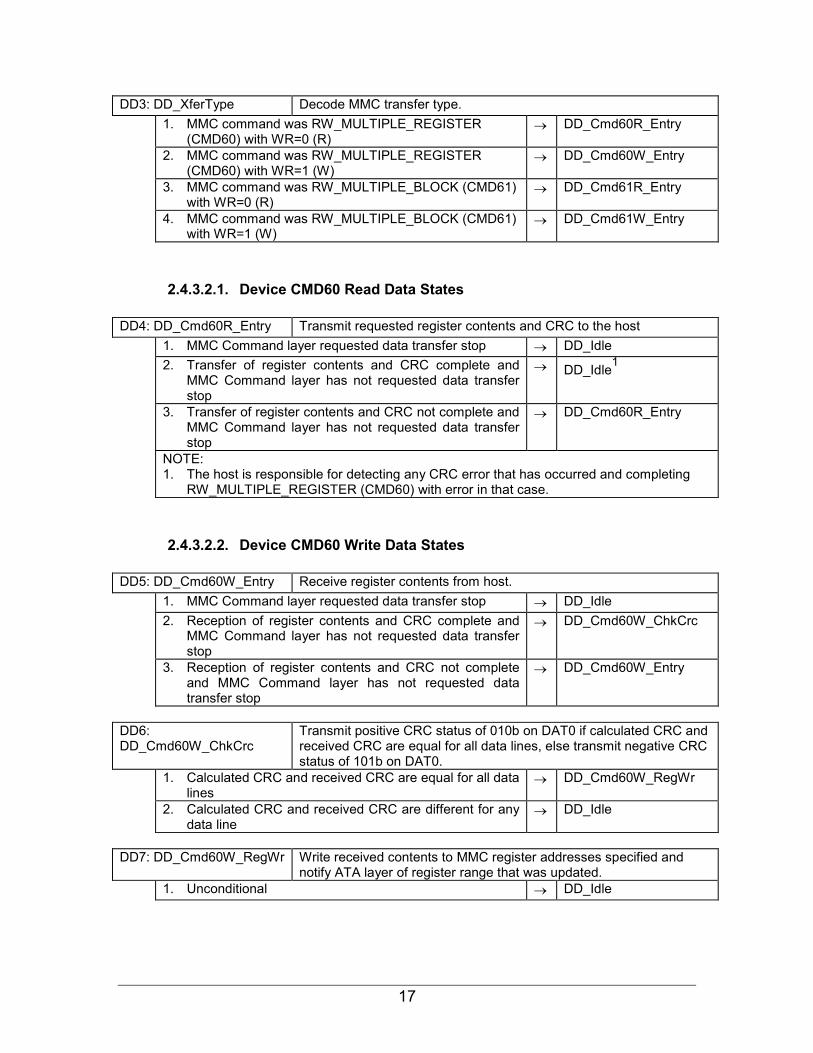
DD3: DD_XferType Decode MMC transfer type. 1. MMC command was RW_MULTIPLE_REGISTER
(CMD60) with WR=0 (R) → DD_Cmd60R_Entry
2. MMC command was RW_MULTIPLE_REGISTER (CMD60) with WR=1 (W)
→ DD_Cmd60W_Entry
3. MMC command was RW_MULTIPLE_BLOCK (CMD61) with WR=0 (R)
→ DD_Cmd61R_Entry
4. MMC command was RW_MULTIPLE_BLOCK (CMD61) with WR=1 (W)
→ DD_Cmd61W_Entry
2.4.3.2.1. Device CMD60 Read Data States DD4: DD_Cmd60R_Entry Transmit requested register contents and CRC to the host
1. MMC Command layer requested data transfer stop → DD_Idle 2. Transfer of register contents and CRC complete and
MMC Command layer has not requested data transfer stop
→ DD_Idle1
3. Transfer of register contents and CRC not complete and MMC Command layer has not requested data transfer stop
→ DD_Cmd60R_Entry
NOTE: 1. The host is responsible for detecting any CRC error that has occurred and completing
RW_MULTIPLE_REGISTER (CMD60) with error in that case.
2.4.3.2.2. Device CMD60 Write Data States DD5: DD_Cmd60W_Entry Receive register contents from host.
1. MMC Command layer requested data transfer stop → DD_Idle 2. Reception of register contents and CRC complete and
MMC Command layer has not requested data transfer stop
→ DD_Cmd60W_ChkCrc
3. Reception of register contents and CRC not complete and MMC Command layer has not requested data transfer stop
→ DD_Cmd60W_Entry
DD6: DD_Cmd60W_ChkCrc
Transmit positive CRC status of 010b on DAT0 if calculated CRC and received CRC are equal for all data lines, else transmit negative CRC status of 101b on DAT0.
1. Calculated CRC and received CRC are equal for all data lines
→ DD_Cmd60W_RegWr
2. Calculated CRC and received CRC are different for any data line
→ DD_Idle
DD7: DD_Cmd60W_RegWr Write received contents to MMC register addresses specified and notify ATA layer of register range that was updated.
1. Unconditional → DD_Idle
18
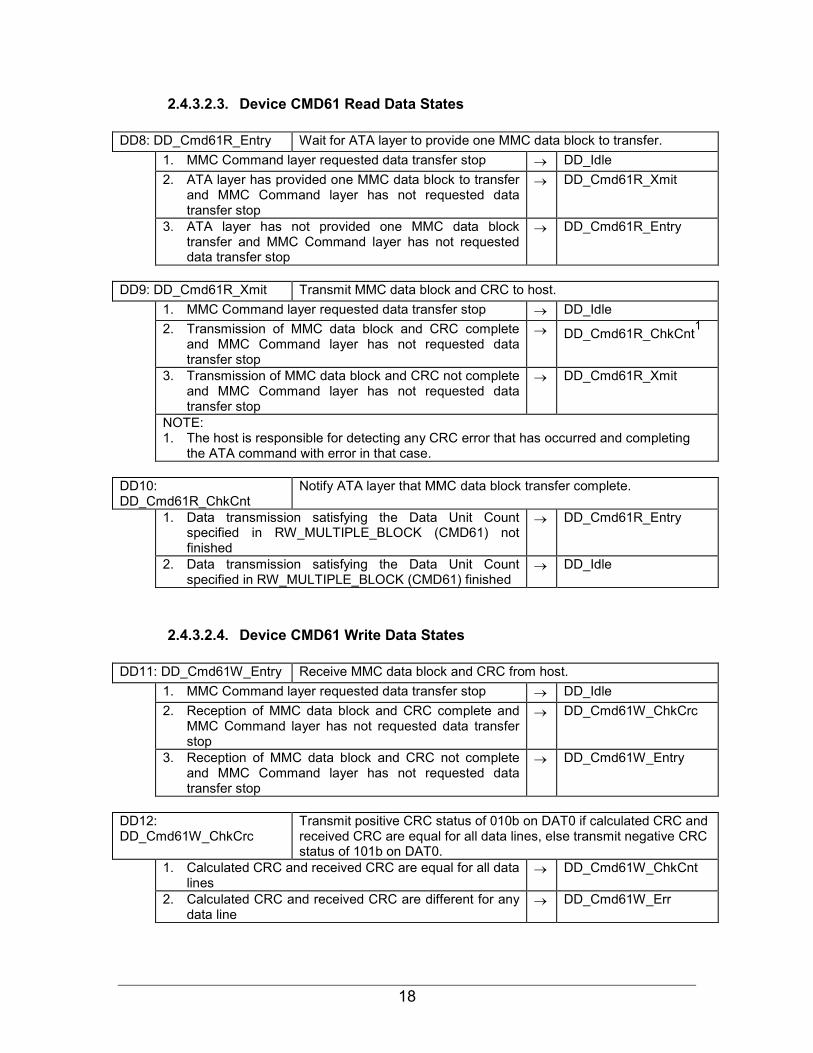
2.4.3.2.3. Device CMD61 Read Data States DD8: DD_Cmd61R_Entry Wait for ATA layer to provide one MMC data block to transfer.
1. MMC Command layer requested data transfer stop → DD_Idle 2. ATA layer has provided one MMC data block to transfer
and MMC Command layer has not requested data transfer stop
→ DD_Cmd61R_Xmit
3. ATA layer has not provided one MMC data block transfer and MMC Command layer has not requested data transfer stop
→ DD_Cmd61R_Entry
DD9: DD_Cmd61R_Xmit Transmit MMC data block and CRC to host. 1. MMC Command layer requested data transfer stop → DD_Idle 2. Transmission of MMC data block and CRC complete
and MMC Command layer has not requested data transfer stop
→ DD_Cmd61R_ChkCnt1
3. Transmission of MMC data block and CRC not complete and MMC Command layer has not requested data transfer stop
→ DD_Cmd61R_Xmit
NOTE: 1. The host is responsible for detecting any CRC error that has occurred and completing
the ATA command with error in that case.
DD10: DD_Cmd61R_ChkCnt
Notify ATA layer that MMC data block transfer complete.
1. Data transmission satisfying the Data Unit Count specified in RW_MULTIPLE_BLOCK (CMD61) not finished
→ DD_Cmd61R_Entry
2. Data transmission satisfying the Data Unit Count specified in RW_MULTIPLE_BLOCK (CMD61) finished
→ DD_Idle
2.4.3.2.4. Device CMD61 Write Data States DD11: DD_Cmd61W_Entry Receive MMC data block and CRC from host.
1. MMC Command layer requested data transfer stop → DD_Idle 2. Reception of MMC data block and CRC complete and
MMC Command layer has not requested data transfer stop
→ DD_Cmd61W_ChkCrc
3. Reception of MMC data block and CRC not complete and MMC Command layer has not requested data transfer stop
→ DD_Cmd61W_Entry
DD12: DD_Cmd61W_ChkCrc
Transmit positive CRC status of 010b on DAT0 if calculated CRC and received CRC are equal for all data lines, else transmit negative CRC status of 101b on DAT0.
1. Calculated CRC and received CRC are equal for all data lines
→ DD_Cmd61W_ChkCnt
2. Calculated CRC and received CRC are different for any data line
→ DD_Cmd61W_Err
19
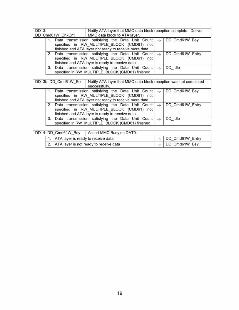
DD13: DD_Cmd61W_ChkCnt
Notify ATA layer that MMC data block reception complete. Deliver MMC data block to ATA layer.
1. Data transmission satisfying the Data Unit Count specified in RW_MULTIPLE_BLOCK (CMD61) not finished and ATA layer not ready to receive more data
→ DD_Cmd61W_Bsy
2. Data transmission satisfying the Data Unit Count specified in RW_MULTIPLE_BLOCK (CMD61) not finished and ATA layer is ready to receive data
→ DD_Cmd61W_Entry
3. Data transmission satisfying the Data Unit Count specified in RW_MULTIPLE_BLOCK (CMD61) finished
→ DD_Idle
DD13b: DD_Cmd61W_Err Notify ATA layer that MMC data block reception was not completed successfully.
1. Data transmission satisfying the Data Unit Count specified in RW_MULTIPLE_BLOCK (CMD61) not finished and ATA layer not ready to receive more data
→ DD_Cmd61W_Bsy
2. Data transmission satisfying the Data Unit Count specified in RW_MULTIPLE_BLOCK (CMD61) not finished and ATA layer is ready to receive data
→ DD_Cmd61W_Entry
3. Data transmission satisfying the Data Unit Count specified in RW_MULTIPLE_BLOCK (CMD61) finished
→ DD_Idle
DD14: DD_Cmd61W_Bsy Assert MMC Busy on DAT0. 1. ATA layer is ready to receive data → DD_Cmd61W_Entry 2. ATA layer is not ready to receive data → DD_Cmd61W_Bsy
20
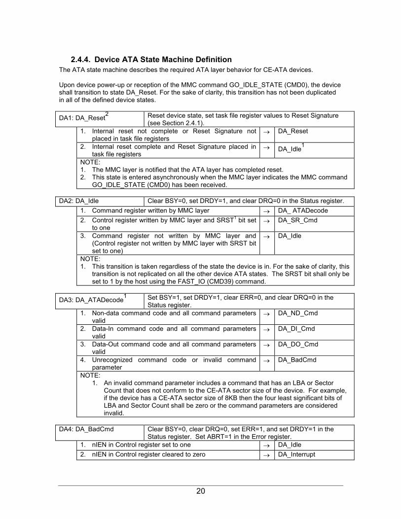
2.4.4. Device ATA State Machine Definition The ATA state machine describes the required ATA layer behavior for CE-ATA devices. Upon device power-up or reception of the MMC command GO_IDLE_STATE (CMD0), the device shall transition to state DA_Reset. For the sake of clarity, this transition has not been duplicated in all of the defined device states. DA1: DA_Reset2 Reset device state, set task file register values to Reset Signature
(see Section 2.4.1).
1. Internal reset not complete or Reset Signature not placed in task file registers
→ DA_Reset
2. Internal reset complete and Reset Signature placed in task file registers
→ DA_Idle1
NOTE: 1. The MMC layer is notified that the ATA layer has completed reset. 2. This state is entered asynchronously when the MMC layer indicates the MMC command
GO_IDLE_STATE (CMD0) has been received.
DA2: DA_Idle Clear BSY=0, set DRDY=1, and clear DRQ=0 in the Status register. 1. Command register written by MMC layer → DA_ ATADecode 2. Control register written by MMC layer and SRST1 bit set
to one → DA_SR_Cmd
3. Command register not written by MMC layer and (Control register not written by MMC layer with SRST bit set to one)
→ DA_Idle
NOTE: 1. This transition is taken regardless of the state the device is in. For the sake of clarity, this
transition is not replicated on all the other device ATA states. The SRST bit shall only be set to 1 by the host using the FAST_IO (CMD39) command.
DA3: DA_ATADecode1 Set BSY=1, set DRDY=1, clear ERR=0, and clear DRQ=0 in the Status register.
1. Non-data command code and all command parameters valid
→ DA_ND_Cmd
2. Data-In command code and all command parameters valid
→ DA_DI_Cmd
3. Data-Out command code and all command parameters valid
→ DA_DO_Cmd
4. Unrecognized command code or invalid command parameter
→ DA_BadCmd
NOTE: 1. An invalid command parameter includes a command that has an LBA or Sector
Count that does not conform to the CE-ATA sector size of the device. For example, if the device has a CE-ATA sector size of 8KB then the four least significant bits of LBA and Sector Count shall be zero or the command parameters are considered invalid.
DA4: DA_BadCmd Clear BSY=0, clear DRQ=0, set ERR=1, and set DRDY=1 in the Status register. Set ABRT=1 in the Error register.
1. nIEN in Control register set to one → DA_Idle 2. nIEN in Control register cleared to zero → DA_Interrupt
21
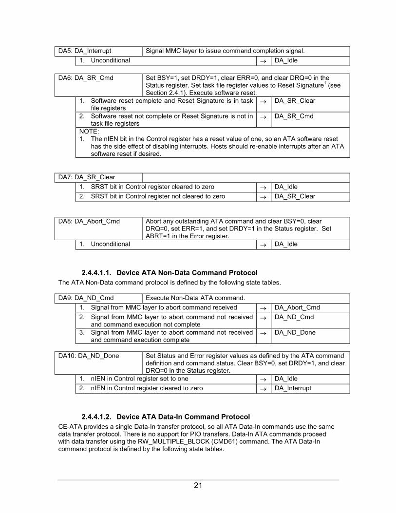
DA5: DA_Interrupt Signal MMC layer to issue command completion signal. 1. Unconditional → DA_Idle
DA6: DA_SR_Cmd Set BSY=1, set DRDY=1, clear ERR=0, and clear DRQ=0 in the Status register. Set task file register values to Reset Signature1 (see Section 2.4.1). Execute software reset.
1. Software reset complete and Reset Signature is in task file registers
→ DA_SR_Clear
2. Software reset not complete or Reset Signature is not in task file registers
→ DA_SR_Cmd
NOTE: 1. The nIEN bit in the Control register has a reset value of one, so an ATA software reset
has the side effect of disabling interrupts. Hosts should re-enable interrupts after an ATA software reset if desired.
DA7: DA_SR_Clear
1. SRST bit in Control register cleared to zero → DA_Idle 2. SRST bit in Control register not cleared to zero → DA_SR_Clear
DA8: DA_Abort_Cmd Abort any outstanding ATA command and clear BSY=0, clear DRQ=0, set ERR=1, and set DRDY=1 in the Status register. Set ABRT=1 in the Error register.
1. Unconditional → DA_Idle
2.4.4.1.1. Device ATA Non-Data Command Protocol The ATA Non-Data command protocol is defined by the following state tables. DA9: DA_ND_Cmd Execute Non-Data ATA command.
1. Signal from MMC layer to abort command received → DA_Abort_Cmd 2. Signal from MMC layer to abort command not received
and command execution not complete → DA_ND_Cmd
3. Signal from MMC layer to abort command not received and command execution complete
→ DA_ND_Done
DA10: DA_ND_Done Set Status and Error register values as defined by the ATA command definition and command status. Clear BSY=0, set DRDY=1, and clear DRQ=0 in the Status register.
1. nIEN in Control register set to one → DA_Idle 2. nIEN in Control register cleared to zero → DA_Interrupt
2.4.4.1.2. Device ATA Data-In Command Protocol CE-ATA provides a single Data-In transfer protocol, so all ATA Data-In commands use the same data transfer protocol. There is no support for PIO transfers. Data-In ATA commands proceed with data transfer using the RW_MULTIPLE_BLOCK (CMD61) command. The ATA Data-In command protocol is defined by the following state tables.

22
DA11: DA_DI_Cmd Execute Data-In ATA command. 1. Signal from MMC layer to abort command received → DA_Abort_Cmd 2. Signal from MMC layer to abort command not received
and data ready to transmit to host and no error encountered
→ DA_DI_DataXfer
3. Signal from MMC layer to abort command not received and data not ready to transmit to host and no error encountered
→ DA_DI_Cmd
4. Signal from MMC layer to abort command not received and error encountered
→ DA_DI_Done
DA12: DA_DI_DataXfer Clear BSY=0 and set DRQ=1 in the Status register. Signal MMC layer to transmit MMC data block1 and provide MMC data block to MMC layer.
1. Signal from MMC layer to abort command received → DA_Abort_Cmd 2. Signal received from MMC layer that transmission
complete and signal from MMC layer to abort command not received
→ DA_DI_ChkDuCnt
3. Signal from MMC layer that transmission complete not received and signal from MMC layer to abort command not received
→ DA_DI_DataXfer
NOTE: 1. The MMC layer block size and MMC layer Data Unit Count value is exposed to the
ATA layer.
DA13: DA_DI_ChkDuCnt Check if Data Unit Count of RW_MULTIPLE_BLOCK (CMD61) is satisified.
1. Data transmission satisfying the Data Unit Count specified in the RW_MULTIPLE_BLOCK (CMD61) command not finished and (error not encountered or (error encountered and nIEN=1 in the Control register))
→ DA_DI_DataXfer
2. Error encountered and nIEN=0 in the Control register → DA_DI_Done 3. Data transmission satisfying the Data Unit Count
specified in the RW_MULTIPLE_BLOCK (CMD61) command finished and (error not encountered or (error encountered and nIEN=1 in the Control register))
→ DA_DI_ChkDone
DA14: DA_DI_ChkDone Set BSY=1 and clear DRQ=0 in the Status register. Set Status ERR bit and Error register based on current ATA command status.
1. Data transfer length specified in ATA command not satisfied
→ DA_DI_Cmd
2. Data transfer length specified in ATA command satisfied → DA_DI_Done
DA15: DA_DI_Done Set Status and Error register values as defined by the ATA command definition and command status. Clear BSY=0, set DRDY=1, and clear DRQ=0 in the Status register.
1. nIEN in Control register set to one → DA_Idle 2. nIEN in Control register cleared to zero → DA_Interrupt
23
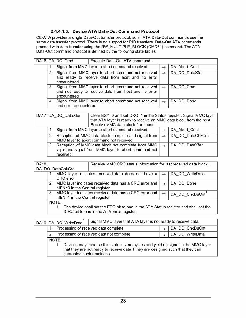
2.4.4.1.3. Device ATA Data-Out Command Protocol CE-ATA provides a single Data-Out transfer protocol, so all ATA Data-Out commands use the same data transfer protocol. There is no support for PIO transfers. Data-Out ATA commands proceed with data transfer using the RW_MULTIPLE_BLOCK (CMD61) command. The ATA Data-Out command protocol is defined by the following state tables. DA16: DA_DO_Cmd Execute Data-Out ATA command.
1. Signal from MMC layer to abort command received → DA_Abort_Cmd 2. Signal from MMC layer to abort command not received
and ready to receive data from host and no error encountered
→ DA_DO_DataXfer
3. Signal from MMC layer to abort command not received and not ready to receive data from host and no error encountered
→ DA_DO_Cmd
4. Signal from MMC layer to abort command not received and error encountered
→ DA_DO_Done
DA17: DA_DO_DataXfer Clear BSY=0 and set DRQ=1 in the Status register. Signal MMC layer that ATA layer is ready to receive an MMC data block from the host. Receive MMC data block from host.
1. Signal from MMC layer to abort command received → DA_Abort_Cmd 2. Reception of MMC data block complete and signal from
MMC layer to abort command not received → DA_DO_DataChkCrc
3. Reception of MMC data block not complete from MMC layer and signal from MMC layer to abort command not received
→ DA_DO_DataXfer
DA18: DA_DO_DataChkCrc
Receive MMC CRC status information for last received data block.
1. MMC layer indicates received data does not have a CRC error
→ DA_DO_WriteData
2. MMC layer indicates received data has a CRC error and nIEN=0 in the Control register
→ DA_DO_Done
3. MMC layer indicates received data has a CRC error and nIEN=1 in the Control register
→ DA_DO_ChkDuCnt1
NOTE: 1. The device shall set the ERR bit to one in the ATA Status register and shall set the
ICRC bit to one in the ATA Error register.
DA19: DA_DO_WriteData1 Signal MMC layer that ATA layer is not ready to receive data.
1. Processing of received data complete → DA_DO_ChkDuCnt 2. Processing of received data not complete → DA_DO_WriteData NOTE:
1. Devices may traverse this state in zero cycles and yield no signal to the MMC layer that they are not ready to receive data if they are designed such that they can guarantee such readiness.
24
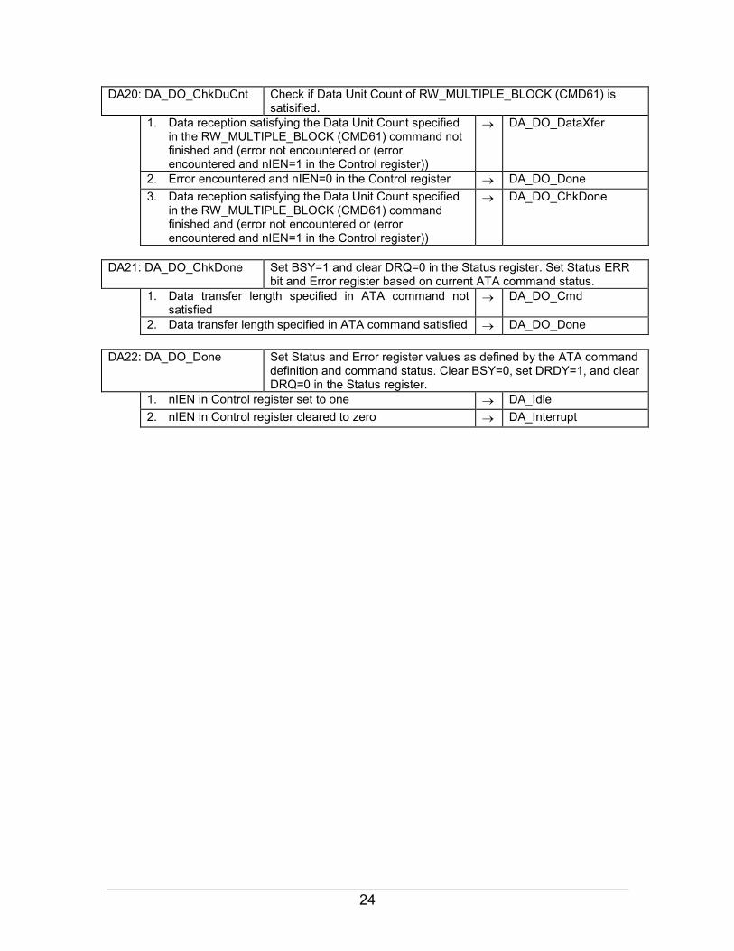
DA20: DA_DO_ChkDuCnt Check if Data Unit Count of RW_MULTIPLE_BLOCK (CMD61) is satisified.
1. Data reception satisfying the Data Unit Count specified in the RW_MULTIPLE_BLOCK (CMD61) command not finished and (error not encountered or (error encountered and nIEN=1 in the Control register))
→ DA_DO_DataXfer
2. Error encountered and nIEN=0 in the Control register → DA_DO_Done 3. Data reception satisfying the Data Unit Count specified
in the RW_MULTIPLE_BLOCK (CMD61) command finished and (error not encountered or (error encountered and nIEN=1 in the Control register))
→ DA_DO_ChkDone
DA21: DA_DO_ChkDone Set BSY=1 and clear DRQ=0 in the Status register. Set Status ERR bit and Error register based on current ATA command status.
1. Data transfer length specified in ATA command not satisfied
→ DA_DO_Cmd
2. Data transfer length specified in ATA command satisfied → DA_DO_Done
DA22: DA_DO_Done Set Status and Error register values as defined by the ATA command definition and command status. Clear BSY=0, set DRDY=1, and clear DRQ=0 in the Status register.
1. nIEN in Control register set to one → DA_Idle 2. nIEN in Control register cleared to zero → DA_Interrupt
25
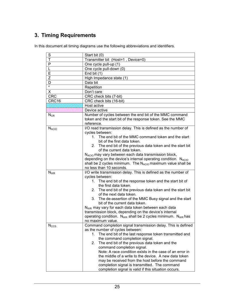
3. Timing Requirements In this document all timing diagrams use the following abbreviations and identifiers.
S Start bit (0) T Transmitter bit (Host=1 , Device=0) P One cycle pull-up (1) L One cycle pull-down (0) E End bit (1) Z High Impedance state (1) D Data bit * Repetition X Don’t care CRC CRC check bits (7-bit) CRC16 CRC check bits (16-bit)
Host active Device active
NCR Number of cycles between the end bit of the MMC command token and the start bit of the response token. See the MMC reference.
NACIO I/O read transmission delay. This is defined as the number of cycles between:
1. The end bit of the MMC command token and the start bit of the first data token.
2. The end bit of the previous data token and the start bit of the current data token.
NACIO may vary between each data transmission block, depending on the device’s internal operating condition. NACIO shall be 2 cycles minimum. The NACIO maximum value shall be no less than 10 seconds.
NWR I/O write transmission delay. This is defined as the number of cycles between:
1. The end bit of the response token and the start bit of the first data token.
2. The end bit of the previous data token and the start bit of the next data token.
3. The de-assertion of the MMC Busy signal and the start bit of the current data token.
NWR may vary for each data token between each data transmission block, depending on the device’s internal operating condition. NWR shall be 2 cycles minimum. NWR has no maximum value.
NCCS Command completion signal transmission delay. This is defined as the number of cycles between:
1. The end bit of the last response token transmitted and the command completion signal.
2. The end bit of the previous data token and the command completion signal. Note: A race condition exists in the case of an error in the middle of a write to the device. A new data token may be received from the host before the command completion signal is transmitted. The command completion signal is valid if this situation occurs.
26
NCCS may vary for each ATA command, depending on the device’s internal operating condition. NCCS shall be 8 cycles minimum after a previous response token. NCCS shall be 2 cycles minimum after a previous data token. NCCS has no maximum value.
NRC Number of cycles between the end bit of the response token and the start bit of the next MMC command token. See the MMC reference.
NCC Number of cycles between the end bit of the preceding MMC command token and the start bit of the next MMC command token. See the MMC reference.
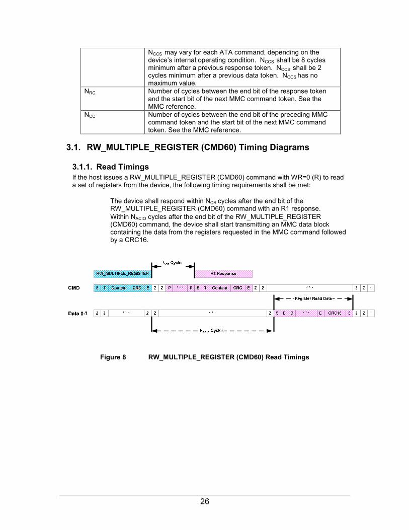
3.1. RW_MULTIPLE_REGISTER (CMD60) Timing Diagrams
3.1.1. Read Timings If the host issues a RW_MULTIPLE_REGISTER (CMD60) command with WR=0 (R) to read a set of registers from the device, the following timing requirements shall be met:
• The device shall respond within NCR cycles after the end bit of the RW_MULTIPLE_REGISTER (CMD60) command with an R1 response.
• Within NACIO cycles after the end bit of the RW_MULTIPLE_REGISTER (CMD60) command, the device shall start transmitting an MMC data block containing the data from the registers requested in the MMC command followed by a CRC16.
Figure 8 RW_MULTIPLE_REGISTER (CMD60) Read Timings
27
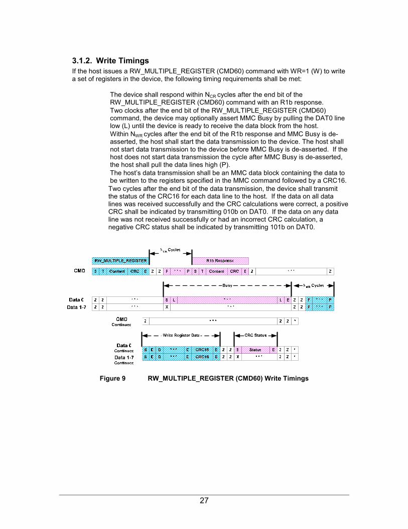
3.1.2. Write Timings If the host issues a RW_MULTIPLE_REGISTER (CMD60) command with WR=1 (W) to write a set of registers in the device, the following timing requirements shall be met:
• The device shall respond within NCR cycles after the end bit of the RW_MULTIPLE_REGISTER (CMD60) command with an R1b response.
• Two clocks after the end bit of the RW_MULTIPLE_REGISTER (CMD60) command, the device may optionally assert MMC Busy by pulling the DAT0 line low (L) until the device is ready to receive the data block from the host.
• Within NWR cycles after the end bit of the R1b response and MMC Busy is de-asserted, the host shall start the data transmission to the device. The host shall not start data transmission to the device before MMC Busy is de-asserted. If the host does not start data transmission the cycle after MMC Busy is de-asserted, the host shall pull the data lines high (P).
• The host’s data transmission shall be an MMC data block containing the data to be written to the registers specified in the MMC command followed by a CRC16.
• Two cycles after the end bit of the data transmission, the device shall transmit the status of the CRC16 for each data line to the host. If the data on all data lines was received successfully and the CRC calculations were correct, a positive CRC shall be indicated by transmitting 010b on DAT0. If the data on any data line was not received successfully or had an incorrect CRC calculation, a negative CRC status shall be indicated by transmitting 101b on DAT0.
Figure 9 RW_MULTIPLE_REGISTER (CMD60) Write Timings

28
3.2. RW_MULTIPLE_BLOCK (CMD61) Timing Diagrams
3.2.1. Read Single Block Timings The host issues a RW_MULTIPLE_BLOCK (CMD61) command to transfer blocks of data from the device. Each MMC data block shall be 512 bytes, 1KB, or 4KB in size with a CRC16 appended to each data line. The amount of data to transfer is specified in the Data Unit Count field of the RW_MULTIPLE_BLOCK (CMD61) command. Before issuing the RW_MULTIPLE_BLOCK (CMD61) command, the host must previously have issued the ATA command to the device using RW_MULTIPLE_REGISTER (CMD60). The following timing requirements shall be met for the RW_MULTIPLE_BLOCK (CMD61) command with WR=0 (R).
• The device shall respond within NCR cycles after the end bit of the
RW_MULTIPLE_BLOCK (CMD61) command with an R1 response. • Within NACIO cycles after the end bit of the RW_MULTIPLE_BLOCK (CMD61)
command, the device shall start transmitting an MMC data block containing the data requested in the ATA command followed by a CRC16 on each data line.
• If interrupts are enabled (nIEN=0 in the ATA Control register), the device shall transmit the start bit of the command completion signal within NCCS cycles after the end bit of the data transmission.
Figure 10 RW_MULTIPLE_BLOCK (CMD61) Single Block Read Timings
29
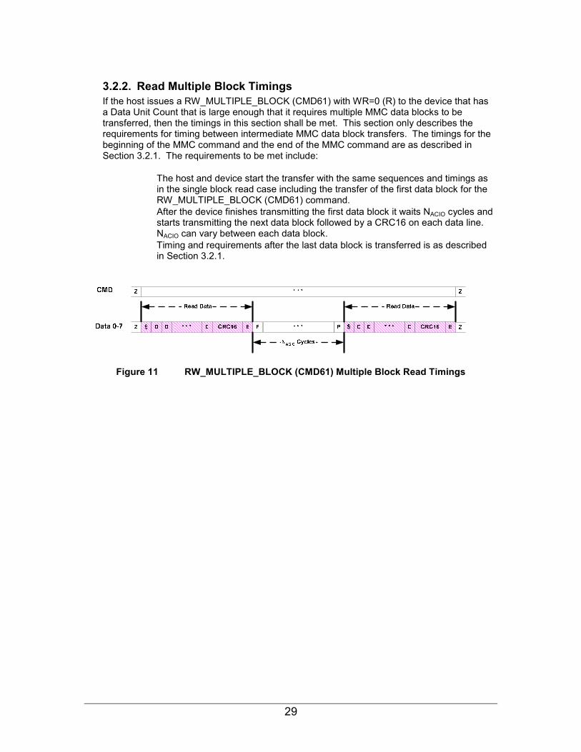
3.2.2. Read Multiple Block Timings If the host issues a RW_MULTIPLE_BLOCK (CMD61) with WR=0 (R) to the device that has a Data Unit Count that is large enough that it requires multiple MMC data blocks to be transferred, then the timings in this section shall be met. This section only describes the requirements for timing between intermediate MMC data block transfers. The timings for the beginning of the MMC command and the end of the MMC command are as described in Section 3.2.1. The requirements to be met include:
• The host and device start the transfer with the same sequences and timings as in the single block read case including the transfer of the first data block for the RW_MULTIPLE_BLOCK (CMD61) command.
• After the device finishes transmitting the first data block it waits NACIO cycles and starts transmitting the next data block followed by a CRC16 on each data line. NACIO can vary between each data block.
• Timing and requirements after the last data block is transferred is as described in Section 3.2.1.
Figure 11 RW_MULTIPLE_BLOCK (CMD61) Multiple Block Read Timings
30
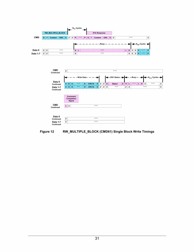
3.2.3. Write Single Block Timings The host issues a RW_MULTIPLE_BLOCK (CMD61) command to transfer blocks of data to the device. Each MMC data block shall be 512 bytes, 1KB, or 4KB in size with a CRC16 appended to each data line. The amount of data to transfer is specified in the Data Unit Count field of the RW_MULTIPLE_BLOCK (CMD61) command. Before issuing the RW_MULTIPLE_BLOCK (CMD61) command, the host must previously have issued the ATA command to the device using RW_MULTIPLE_REGISTER (CMD60). The following timing requirements shall be met for a RW_MULTIPLE_BLOCK (CMD61) with WR=1 (W).
• The device shall respond within NCR cycles after the end bit of the
RW_MULTIPLE_BLOCK (CMD61) command with an R1b response. • Two clocks after the end bit of the RW_MULTIPLE_BLOCK (CMD61) command,
the device may optionally assert MMC Busy by pulling the DAT0 line low (L) until the device is ready to receive the data block from the host.
• Within NWR cycles after the end bit of the R1b response and MMC Busy is de-asserted, the host shall start transmitting an MMC data block containing the data to be written as part of the ATA command followed by a CRC16 on each data line. The host shall not start data transmission to the device before the end bit of the R1b response is received and MMC Busy is de-asserted. If the host does not start data transmission the cycle after MMC Busy is de-asserted, the host shall pull the data lines high (P).
• The host’s data transmission shall be an MMC data block containing the data to be written to the device followed by a CRC16.
• Two cycles after the end bit of the data transmission, the device shall transmit the status of the CRC16 for each data line individually to the host. If the data on all data lines was received successfully and the CRC calculations were correct, a positive CRC shall be indicated by transmitting 010b on DAT0. If the data on any data line was not received successfully or had an incorrect CRC calculation, a negative CRC status shall be indicated by transmitting 101b on DAT0.
• Immediately after the end bit of the CRC status is transmitted, the device may optionally assert MMC Busy.
• If interrupts are enabled (nIEN=0 in the ATA Control register), the device shall transmit the start bit of the command completion signal within NCCS cycles after the end bit of the data transmission and MMC Busy is de-asserted.
31
S T Content
RW_MULTIPLE_BLOCK
CRC E ZZ P * * * P
R1b Response
S T Content CRC E
* * *
ZZ * * *
Z
ZZ
NCR Cycles
Write Data
D DD * * * CRC16 E
CMD
StatusS E
ZZ * * *
ZZD DD * * * CRC16 E X * * *
CRC Status
CMDContinued
Data 1-7Continued
Data 0Continued
L * * * LS E
Busy
* * * Z
Z
NWR Cycles
P * * * P
P * * * P
ZZ
Z Z
Z * * *
Z
Z
XX * * *
Z
S
S
Data 1-7Data 0
L * * * LS E
Busy
* * *CMDContinued
Data 1-7Continued
Data 0Continued
CommandCompletion
Signal
ZL
Z * * *
NCCS Cycles
* * *Z
* * *Z
Figure 12 RW_MULTIPLE_BLOCK (CMD61) Single Block Write Timings
32
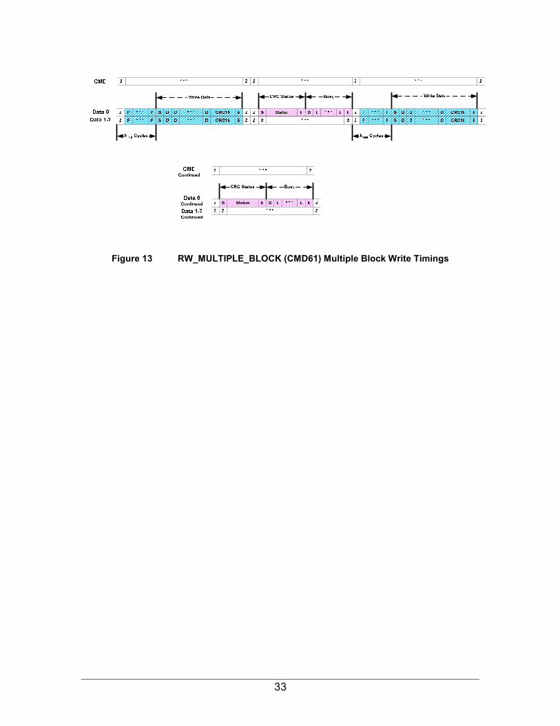
3.2.4. Write Multiple Block Timings If the host issues a RW_MULTIPLE_BLOCK (CMD61) with WR=1 (W) to the device that has a Data Unit Count that is large enough that it requires multiple MMC data blocks to be transferred, then the timings in this section shall be met. This section only describes the requirements for timing between intermediate MMC data block transfers. The timings for the beginning of the MMC command and the end of the MMC command are as described in Section 3.2.3. The requirements to be met include:
• The host and device start the transfer with the same sequences and timings as in the single block write case including the transfer of the first data block for the RW_MULTIPLE_BLOCK (CMD61) command. In Figure 13 the first block of write data corresponds to the data transfer portion of the single block write case.
• Two cycles after the end bit of the data transmission for the first data block, the device shall transmit the status of the CRC16 for each data line individually to the host. If the data on all data lines was received successfully and the CRC calculations were correct, a positive CRC shall be indicated by transmitting 010b on DAT0. If the data on any data line was not received successfully or had an incorrect CRC calculation, a negative CRC status shall be indicated by transmitting 101b on DAT0.
• Immediately after transmission of the CRC status is complete on DAT0, the device may optionally assert MMC Busy by pulling the DAT0 line low (L) until it is ready to receive the next MMC data block from the host.
• Within NWR cycles after the host finishes transmitting the first data block and MMC Busy is de-asserted, the host shall start transmitting the second MMC data block. The host shall not start data transmission to the device before MMC Busy is de-asserted. If the host does not start data transmission the cycle after MMC Busy is de-asserted, the host shall pull the data lines high (P).
• Two cycles after the end bit of the data transmission for the second data block, the device shall transmit the status of the CRC16 for each data line individually to the host. If the data on all data lines was received successfully and the CRC calculations were correct, a positive CRC shall be indicated by transmitting 010b on DAT0. If the data on any data line was not received successfully or had an incorrect CRC calculation, a negative CRC status shall be indicated by transmitting 101b on DAT0.
• Immediately after transmission of the CRC status is complete on DAT0, the device may optionally assert MMC Busy by pulling the DAT0 line low (L) until it is ready to receive the next MMC data block from the host.
• Timing and requirements after the last MMC data block is transferred is as described in Section 3.2.3.
33
Figure 13 RW_MULTIPLE_BLOCK (CMD61) Multiple Block Write Timings
34
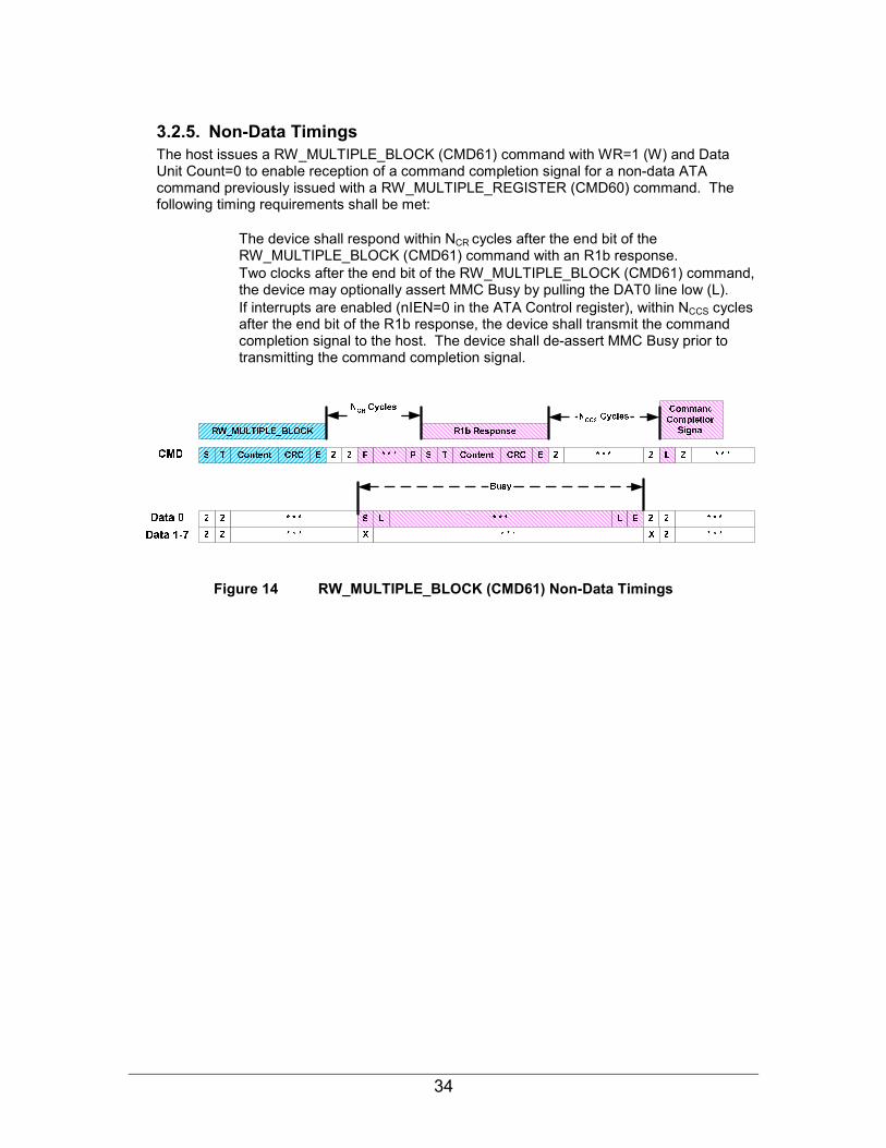
3.2.5. Non-Data Timings The host issues a RW_MULTIPLE_BLOCK (CMD61) command with WR=1 (W) and Data Unit Count=0 to enable reception of a command completion signal for a non-data ATA command previously issued with a RW_MULTIPLE_REGISTER (CMD60) command. The following timing requirements shall be met:
• The device shall respond within NCR cycles after the end bit of the
RW_MULTIPLE_BLOCK (CMD61) command with an R1b response. • Two clocks after the end bit of the RW_MULTIPLE_BLOCK (CMD61) command,
the device may optionally assert MMC Busy by pulling the DAT0 line low (L). • If interrupts are enabled (nIEN=0 in the ATA Control register), within NCCS cycles
after the end bit of the R1b response, the device shall transmit the command completion signal to the host. The device shall de-assert MMC Busy prior to transmitting the command completion signal.
Figure 14 RW_MULTIPLE_BLOCK (CMD61) Non-Data Timings
35
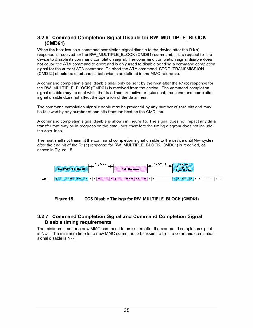
3.2.6. Command Completion Signal Disable for RW_MULTIPLE_BLOCK (CMD61)
When the host issues a command completion signal disable to the device after the R1(b) response is received for the RW_MULTIPLE_BLOCK (CMD61) command, it is a request for the device to disable its command completion signal. The command completion signal disable does not cause the ATA command to abort and is only used to disable sending a command completion signal for the current ATA command. To abort the ATA command, STOP_TRANSMISSION (CMD12) should be used and its behavior is as defined in the MMC reference. A command completion signal disable shall only be sent by the host after the R1(b) response for the RW_MULTIPLE_BLOCK (CMD61) is received from the device. The command completion signal disable may be sent while the data lines are active or quiescent; the command completion signal disable does not affect the operation of the data lines. The command completion signal disable may be preceded by any number of zero bits and may be followed by any number of one bits from the host on the CMD line. A command completion signal disable is shown in Figure 15. The signal does not impact any data transfer that may be in progress on the data lines; therefore the timing diagram does not include the data lines. The host shall not transmit the command completion signal disable to the device until NRC cycles after the end bit of the R1(b) response for RW_MULTIPLE_BLOCK (CMD61) is received, as shown in Figure 15.
Figure 15 CCS Disable Timings for RW_MULTIPLE_BLOCK (CMD61)
3.2.7. Command Completion Signal and Command Completion Signal Disable timing requirements
The minimum time for a new MMC command to be issued after the command completion signal is NRC. The minimum time for a new MMC command to be issued after the command completion signal disable is NCC.
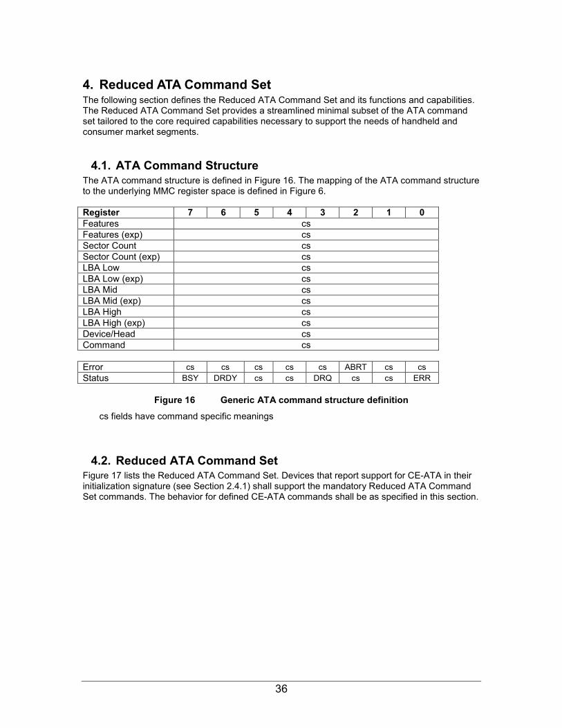
36
4. Reduced ATA Command Set The following section defines the Reduced ATA Command Set and its functions and capabilities. The Reduced ATA Command Set provides a streamlined minimal subset of the ATA command set tailored to the core required capabilities necessary to support the needs of handheld and consumer market segments.
4.1. ATA Command Structure The ATA command structure is defined in Figure 16. The mapping of the ATA command structure to the underlying MMC register space is defined in Figure 6. Register 7 6 5 4 3 2 1 0 Features cs Features (exp) cs Sector Count cs Sector Count (exp) cs LBA Low cs LBA Low (exp) cs LBA Mid cs LBA Mid (exp) cs LBA High cs LBA High (exp) cs Device/Head cs Command cs
Error cs cs cs cs cs ABRT cs cs Status BSY DRDY cs cs DRQ cs cs ERR
Figure 16 Generic ATA command structure definition
cs fields have command specific meanings
4.2. Reduced ATA Command Set Figure 17 lists the Reduced ATA Command Set. Devices that report support for CE-ATA in their initialization signature (see Section 2.4.1) shall support the mandatory Reduced ATA Command Set commands. The behavior for defined CE-ATA commands shall be as specified in this section.
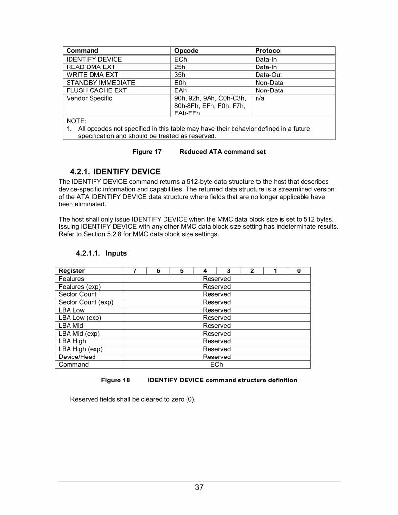
37
Command Opcode Protocol IDENTIFY DEVICE ECh Data-In READ DMA EXT 25h Data-In WRITE DMA EXT 35h Data-Out STANDBY IMMEDIATE E0h Non-Data FLUSH CACHE EXT EAh Non-Data Vendor Specific 90h, 92h, 9Ah, C0h-C3h,
80h-8Fh, EFh, F0h, F7h, FAh-FFh
n/a
NOTE: 1. All opcodes not specified in this table may have their behavior defined in a future
specification and should be treated as reserved.
Figure 17 Reduced ATA command set
4.2.1. IDENTIFY DEVICE The IDENTIFY DEVICE command returns a 512-byte data structure to the host that describes device-specific information and capabilities. The returned data structure is a streamlined version of the ATA IDENTIFY DEVICE data structure where fields that are no longer applicable have been eliminated. The host shall only issue IDENTIFY DEVICE when the MMC data block size is set to 512 bytes. Issuing IDENTIFY DEVICE with any other MMC data block size setting has indeterminate results. Refer to Section 5.2.8 for MMC data block size settings.
4.2.1.1. Inputs Register 7 6 5 4 3 2 1 0 Features Reserved Features (exp) Reserved Sector Count Reserved Sector Count (exp) Reserved LBA Low Reserved LBA Low (exp) Reserved LBA Mid Reserved LBA Mid (exp) Reserved LBA High Reserved LBA High (exp) Reserved Device/Head Reserved Command ECh
Figure 18 IDENTIFY DEVICE command structure definition
Reserved fields shall be cleared to zero (0).
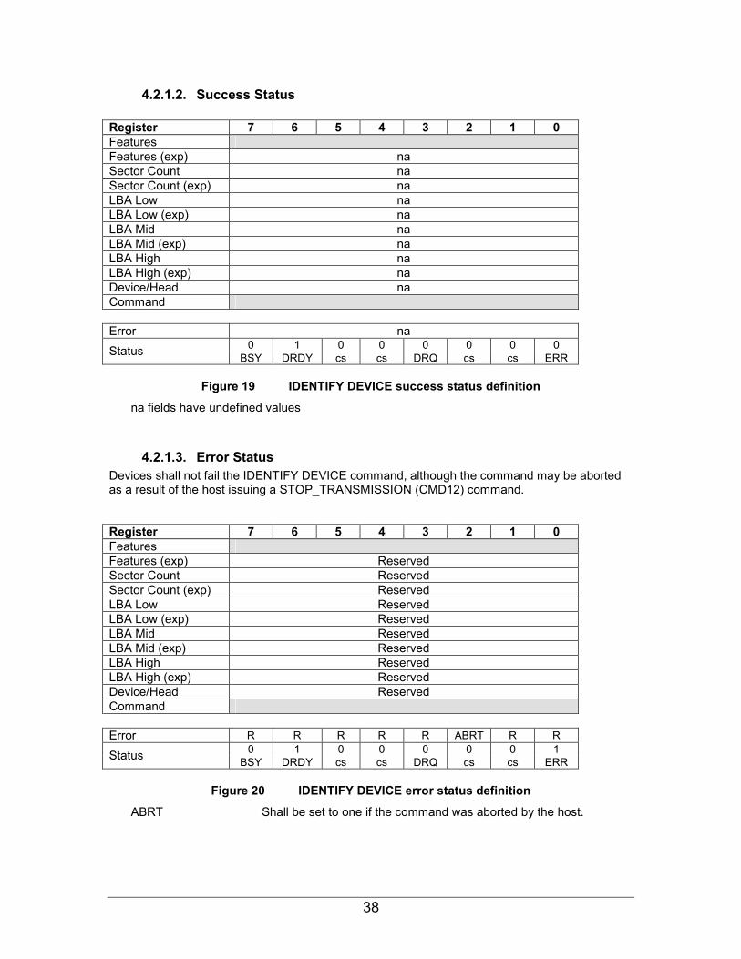
38
4.2.1.2. Success Status Register 7 6 5 4 3 2 1 0 Features Features (exp) na Sector Count na Sector Count (exp) na LBA Low na LBA Low (exp) na LBA Mid na LBA Mid (exp) na LBA High na LBA High (exp) na Device/Head na Command
Error na 0 1 0 0 0 0 0 0Status BSY DRDY cs cs DRQ cs cs ERR
Figure 19 IDENTIFY DEVICE success status definition
na fields have undefined values
4.2.1.3. Error Status Devices shall not fail the IDENTIFY DEVICE command, although the command may be aborted as a result of the host issuing a STOP_TRANSMISSION (CMD12) command.
Register 7 6 5 4 3 2 1 0 Features Features (exp) Reserved Sector Count Reserved Sector Count (exp) Reserved LBA Low Reserved LBA Low (exp) Reserved LBA Mid Reserved LBA Mid (exp) Reserved LBA High Reserved LBA High (exp) Reserved Device/Head Reserved Command
Error R R R R R ABRT R R 0 1 0 0 0 0 0 1Status BSY DRDY cs cs DRQ cs cs ERR
Figure 20 IDENTIFY DEVICE error status definition
ABRT Shall be set to one if the command was aborted by the host.
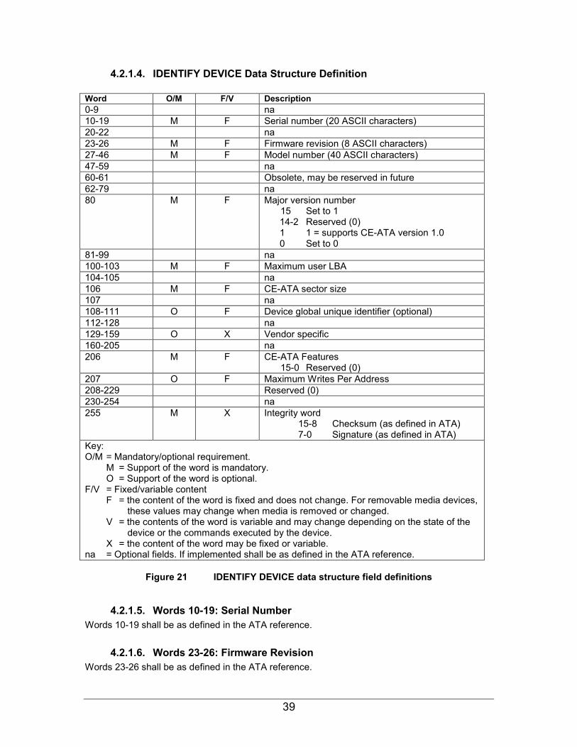
39
4.2.1.4. IDENTIFY DEVICE Data Structure Definition Word O/M F/V Description 0-9 na 10-19 M F Serial number (20 ASCII characters) 20-22 na 23-26 M F Firmware revision (8 ASCII characters) 27-46 M F Model number (40 ASCII characters) 47-59 na 60-61 Obsolete, may be reserved in future 62-79 na 80 M F Major version number
15 Set to 1 14-2 Reserved (0) 1 1 = supports CE-ATA version 1.0 0 Set to 0
81-99 na 100-103 M F Maximum user LBA 104-105 na 106 M F CE-ATA sector size 107 na 108-111 O F Device global unique identifier (optional) 112-128 na 129-159 O X Vendor specific 160-205 na 206 M F CE-ATA Features
15-0 Reserved (0) 207 O F Maximum Writes Per Address 208-229 Reserved (0) 230-254 na 255 M X Integrity word
15-8 Checksum (as defined in ATA) 7-0 Signature (as defined in ATA)
Key: O/M = Mandatory/optional requirement. M = Support of the word is mandatory. O = Support of the word is optional. F/V = Fixed/variable content F = the content of the word is fixed and does not change. For removable media devices,
these values may change when media is removed or changed. V = the contents of the word is variable and may change depending on the state of the
device or the commands executed by the device. X = the content of the word may be fixed or variable. na = Optional fields. If implemented shall be as defined in the ATA reference.
Figure 21 IDENTIFY DEVICE data structure field definitions
4.2.1.5. Words 10-19: Serial Number Words 10-19 shall be as defined in the ATA reference.
4.2.1.6. Words 23-26: Firmware Revision Words 23-26 shall be as defined in the ATA reference.
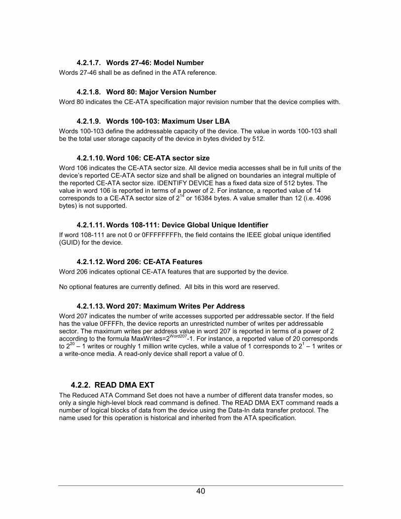
40
4.2.1.7. Words 27-46: Model Number Words 27-46 shall be as defined in the ATA reference.
4.2.1.8. Word 80: Major Version Number Word 80 indicates the CE-ATA specification major revision number that the device complies with.
4.2.1.9. Words 100-103: Maximum User LBA Words 100-103 define the addressable capacity of the device. The value in words 100-103 shall be the total user storage capacity of the device in bytes divided by 512.
4.2.1.10. Word 106: CE-ATA sector size Word 106 indicates the CE-ATA sector size. All device media accesses shall be in full units of the device’s reported CE-ATA sector size and shall be aligned on boundaries an integral multiple of the reported CE-ATA sector size. IDENTIFY DEVICE has a fixed data size of 512 bytes. The value in word 106 is reported in terms of a power of 2. For instance, a reported value of 14 corresponds to a CE-ATA sector size of 214 or 16384 bytes. A value smaller than 12 (i.e. 4096 bytes) is not supported.
4.2.1.11. Words 108-111: Device Global Unique Identifier If word 108-111 are not 0 or 0FFFFFFFFh, the field contains the IEEE global unique identified (GUID) for the device.
4.2.1.12. Word 206: CE-ATA Features Word 206 indicates optional CE-ATA features that are supported by the device. No optional features are currently defined. All bits in this word are reserved.
4.2.1.13. Word 207: Maximum Writes Per Address Word 207 indicates the number of write accesses supported per addressable sector. If the field has the value 0FFFFh, the device reports an unrestricted number of writes per addressable sector. The maximum writes per address value in word 207 is reported in terms of a power of 2 according to the formula MaxWrites=2Word207-1. For instance, a reported value of 20 corresponds to 220 – 1 writes or roughly 1 million write cycles, while a value of 1 corresponds to 21 – 1 writes or a write-once media. A read-only device shall report a value of 0.
4.2.2. READ DMA EXT The Reduced ATA Command Set does not have a number of different data transfer modes, so only a single high-level block read command is defined. The READ DMA EXT command reads a number of logical blocks of data from the device using the Data-In data transfer protocol. The name used for this operation is historical and inherited from the ATA specification.
41
4.2.2.1. Inputs Register 7 6 5 4 3 2 1 0 Features Reserved Features (exp) Reserved Sector Count Sector Count (7:3) 0 0 0 Sector Count (exp) Sector Count (15:8) LBA Low LBA (7:3) 0 0 0 LBA Low (exp) LBA (31:24) LBA Mid LBA (15:8) LBA Mid (exp) LBA (39:32) LBA High LBA (23:16) LBA High (exp) LBA (47:40) Device/Head Reserved Command 25h
Figure 22 READ DMA EXT command structure definition
Sector Count (15:0) Number of 512 byte units of data to be transferred. Hosts shall not specify a value of zero for this field; the device behavior when this value is zero is indeterminate. The Sector Count shall be specified in 512 byte size units and shall be constrained based on the value in Word 106 of IDENTIFY DEVICE. For example, if the Word 106 value is 8KB then Sector Count (3:0) shall be zero.
LBA (47:0) Starting logical block number for the transfer. The LBA shall be specified in 512 byte size units and shall be constrained based on the value in Word 106 of IDENTIFY DEVICE. For example, if the Word 106 value is 8KB then LBA (3:0) shall be zero.
Reserved Reserved fields shall be cleared to zero (0).
42
4.2.2.2. Success Status Register 7 6 5 4 3 2 1 0 Features Features (exp) na Sector Count na Sector Count (exp) na LBA Low LBA (7:0) LBA Low (exp) LBA (31:24) LBA Mid LBA (15:8) LBA Mid (exp) LBA (39:32) LBA High LBA (23:16) LBA High (exp) LBA (47:40) Device/Head na Command
Error na 0 1 0 0 0 SPT OVR 0 Status BSY DRDY cs cs DRQ cs cs ERR
Figure 23 READ DMA EXT success status definition
OVR Shall be set to one if the command encountered an internal device buffer overflow condition due to the host failing to accept data from the device at a sufficiently high rate. This condition is not an error condition although performance is impacted. Hosts with poor interface performance may cause devices to slip revolutions.
SPT If set to one, indicates that at least one block in the LBA region read is considered suspect by the device. The device was able to return correct data, but recommends that the host remap suspect blocks at the next opportunity. If cleared to zero, the device does not consider any of the data blocks suspect.
LBA If SPT is set to one, then the LBA field indicates the first LBA of the first suspect block. There may be more than one suspect block in the region. It is the host’s responsibility to perform additional operations to determine exactly which blocks are suspect. The LBA shall be specified in 512 byte size units and shall be constrained based on the value in Word 106 of IDENTIFY DEVICE.
na fields have undefined values
4.2.2.3. Error Status An unrecoverable error encountered during the execution of this command causes the data transfer to cease at a transfer boundary determined by the device. Except in the case where the host aborts the transfer, the device is required to cease data transfer at an MMC block boundary. Some of the data transferred when an error condition is reported may be incorrect and the host must determine from the status indication the point in the transfer where the error is encountered (and the point at which returned data may be incorrect).
43
Register 7 6 5 4 3 2 1 0 Features Features (exp) Reserved Sector Count Reserved Sector Count (exp) Reserved LBA Low LBA (7:0) LBA Low (exp) LBA (31:24) LBA Mid LBA (15:8) LBA Mid (exp) LBA (39:32) LBA High LBA (23:16) LBA High (exp) LBA (47:40) Device/Head Reserved Command
Error ICRC UNC R IDNF R ABRT R R 0 1 0 0 0 0 OVR 1 Status BSY DRDY cs cs DRQ cs cs ERR
Figure 24 READ DMA EXT error status definition
LBA (47:0) The logical block address of the first unrecoverable error encountered. The LBA shall be specified in 512 byte size units and shall be constrained based on the value in Word 106 of IDENTIFY DEVICE.
ICRC Shall be set to one if an interface communication error occurred during the data transfer.
UNC Shall be set to one if the data from the device media is uncorrectable.
IDNF Shall be set to one if the indicated sector is not user addressable. This is typically as a result of the sector address being past the end of the drive or the specified LBA not adhering to the constraints defined by Word 106 of IDENTIFY DEVICE.
ABRT Shall be set to one if the host aborted the command by issuing the STOP_TRANSMISSION (CMD12) command or if there was an underlying protocol error.
OVR Shall be set to one if the command encountered an internal device buffer overflow condition due to the host failing to accept data from the device at a sufficiently high rate. This condition is not an error condition although performance is impacted. Hosts with poor interface performance may cause devices to slip revolutions.
Reserved/R Reserved fields shall be cleared to zero (0).
4.2.3. WRITE DMA EXT The Reduced ATA Command Set does not have a number of different data transfer modes, so only a single high-level block write command is defined. The WRITE DMA EXT command writes a number of logical blocks of data to the device using the Data-Out data transfer protocol. The name used for this operation is historical and inherited from the ATA specification and there is no DMA transfer distinction. Note that completion of the WRITE DMA EXT command does not necessarily mean that the written data has been committed to the device media. See the FLUSH CACHE EXT command for information on committing written data to media.

44
4.2.3.1. Inputs Register 7 6 5 4 3 2 1 0 Features Reserved Features (exp) Reserved Sector Count Sector Count (7:3) 0 0 0 Sector Count (exp) Sector Count (15:8) LBA Low LBA (7:3) 0 0 0 LBA Low (exp) LBA (31:24) LBA Mid LBA (15:8) LBA Mid (exp) LBA (39:32) LBA High LBA (23:16) LBA High (exp) LBA (47:40) Device/Head Reserved Command 35h
Figure 25 WRITE DMA EXT command structure definition
Sector Count (15:0) Number of 512 byte units of data to be transferred. Hosts shall not specify a value of zero for this field; the device behavior when this value is zero is indeterminate. The Sector Count shall be specified in 512 byte size units and shall be constrained based on the value in Word 106 of IDENTIFY DEVICE. For example, if the Word 106 value is 8KB then Sector Count (3:0) shall be zero.
LBA (47:0) Starting logical block number for the transfer. The LBA shall be specified in 512 byte size units and shall be constrained based on the value in Word 106 of IDENTIFY DEVICE. For example, if the Word 106 value is 8KB then LBA (3:0) shall be zero.
Reserved Reserved fields shall be cleared to zero (0).
45
4.2.3.2. Success Status Register 7 6 5 4 3 2 1 0 Features Features (exp) na Sector Count na Sector Count (exp) na LBA Low LBA (7:0) LBA Low (exp) LBA (31:24) LBA Mid LBA (15:8) LBA Mid (exp) LBA (39:32) LBA High LBA (23:16) LBA High (exp) LBA (47:40) Device/Head na Command
Error na 0 1 0 0 0 SPT UFL 0 Status BSY DRDY cs cs DRQ cs cs ERR
Figure 26 WRITE DMA EXT success status definition
UFL Shall be set to one if the command encountered an internal device buffer underflow condition due to the host failing to deliver data to the device at a sufficiently high rate. This condition is not an error condition although performance is impacted. Hosts with poor interface performance may cause devices to slip revolutions.
SPT If set to one, indicates that at least one block in the LBA region written is considered suspect by the device. The device was able to write correct data, but recommends that the host remap suspect blocks at the next opportunity. If cleared to zero, the device does not consider any of the data blocks suspect.
LBA If SPT is set to one, then the LBA field indicates the first LBA of the first suspect block. There may be more than one suspect block in the region. It is the host’s responsibility to perform additional operations to determine exactly which blocks are suspect. The LBA shall be specified in 512 byte size units and shall be constrained based on the value in Word 106 of IDENTIFY DEVICE.
na fields have undefined values
4.2.3.3. Error Status An unrecoverable error encountered during the execution of this command causes the data transfer to cease at a transfer boundary determined by the device. Some of the data transferred when an error condition is reported may not be written to the device and the host must determine from the status indication the point in the transfer where the error is encountered (and the point at which transferred data may not have been written to the device).
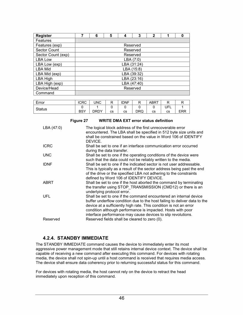
46
Register 7 6 5 4 3 2 1 0 Features Features (exp) Reserved Sector Count Reserved Sector Count (exp) Reserved LBA Low LBA (7:0) LBA Low (exp) LBA (31:24) LBA Mid LBA (15:8) LBA Mid (exp) LBA (39:32) LBA High LBA (23:16) LBA High (exp) LBA (47:40) Device/Head Reserved Command
Error ICRC UNC R IDNF R ABRT R R 0 1 0 0 0 0 UFL 1 Status BSY DRDY cs cs DRQ cs cs ERR
Figure 27 WRITE DMA EXT error status definition
LBA (47:0) The logical block address of the first unrecoverable error encountered. The LBA shall be specified in 512 byte size units and shall be constrained based on the value in Word 106 of IDENTIFY DEVICE.
ICRC Shall be set to one if an interface communication error occurred during the data transfer.
UNC Shall be set to one if the operating conditions of the device were such that the data could not be reliably written to the media.
IDNF Shall be set to one if the indicated sector is not user addressable. This is typically as a result of the sector address being past the end of the drive or the specified LBA not adhering to the constraints defined by Word 106 of IDENTIFY DEVICE.
ABRT Shall be set to one if the host aborted the command by terminating the transfer using STOP_TRANSMISSION (CMD12) or there is an underlying protocol error.
UFL Shall be set to one if the command encountered an internal device buffer underflow condition due to the host failing to deliver data to the device at a sufficiently high rate. This condition is not an error condition although performance is impacted. Hosts with poor interface performance may cause devices to slip revolutions.
Reserved Reserved fields shall be cleared to zero (0).
4.2.4. STANDBY IMMEDIATE The STANDBY IMMEDIATE command causes the device to immediately enter its most aggressive power management mode that still retains internal device context. The device shall be capable of receiving a new command after executing this command. For devices with rotating media, the device shall not spin-up until a host command is received that requires media access. The device shall ensure data coherency prior to returning successful status for this command. For devices with rotating media, the host cannot rely on the device to retract the head immediately upon reception of this command.
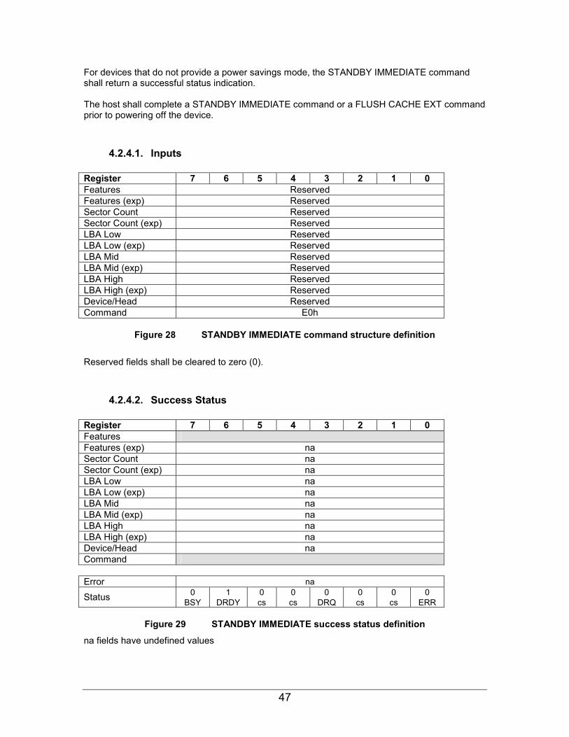
47
For devices that do not provide a power savings mode, the STANDBY IMMEDIATE command shall return a successful status indication. The host shall complete a STANDBY IMMEDIATE command or a FLUSH CACHE EXT command prior to powering off the device.
4.2.4.1. Inputs Register 7 6 5 4 3 2 1 0 Features Reserved Features (exp) Reserved Sector Count Reserved Sector Count (exp) Reserved LBA Low Reserved LBA Low (exp) Reserved LBA Mid Reserved LBA Mid (exp) Reserved LBA High Reserved LBA High (exp) Reserved Device/Head Reserved Command E0h
Figure 28 STANDBY IMMEDIATE command structure definition
Reserved fields shall be cleared to zero (0).
4.2.4.2. Success Status Register 7 6 5 4 3 2 1 0 Features Features (exp) na Sector Count na Sector Count (exp) na LBA Low na LBA Low (exp) na LBA Mid na LBA Mid (exp) na LBA High na LBA High (exp) na Device/Head na Command
Error na 0 1 0 0 0 0 0 0Status BSY DRDY cs cs DRQ cs cs ERR
Figure 29 STANDBY IMMEDIATE success status definition
na fields have undefined values
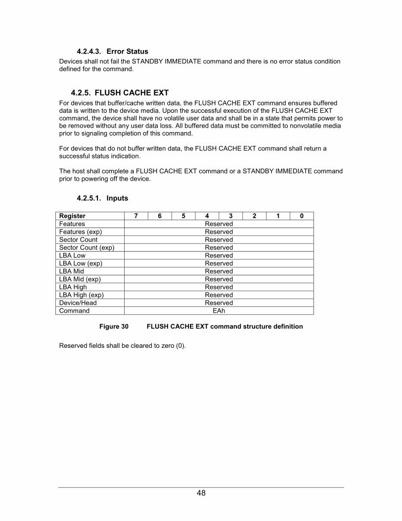
48
4.2.4.3. Error Status Devices shall not fail the STANDBY IMMEDIATE command and there is no error status condition defined for the command.
4.2.5. FLUSH CACHE EXT For devices that buffer/cache written data, the FLUSH CACHE EXT command ensures buffered data is written to the device media. Upon the successful execution of the FLUSH CACHE EXT command, the device shall have no volatile user data and shall be in a state that permits power to be removed without any user data loss. All buffered data must be committed to nonvolatile media prior to signaling completion of this command. For devices that do not buffer written data, the FLUSH CACHE EXT command shall return a successful status indication. The host shall complete a FLUSH CACHE EXT command or a STANDBY IMMEDIATE command prior to powering off the device.
4.2.5.1. Inputs Register 7 6 5 4 3 2 1 0 Features Reserved Features (exp) Reserved Sector Count Reserved Sector Count (exp) Reserved LBA Low Reserved LBA Low (exp) Reserved LBA Mid Reserved LBA Mid (exp) Reserved LBA High Reserved LBA High (exp) Reserved Device/Head Reserved Command EAh
Figure 30 FLUSH CACHE EXT command structure definition
Reserved fields shall be cleared to zero (0).
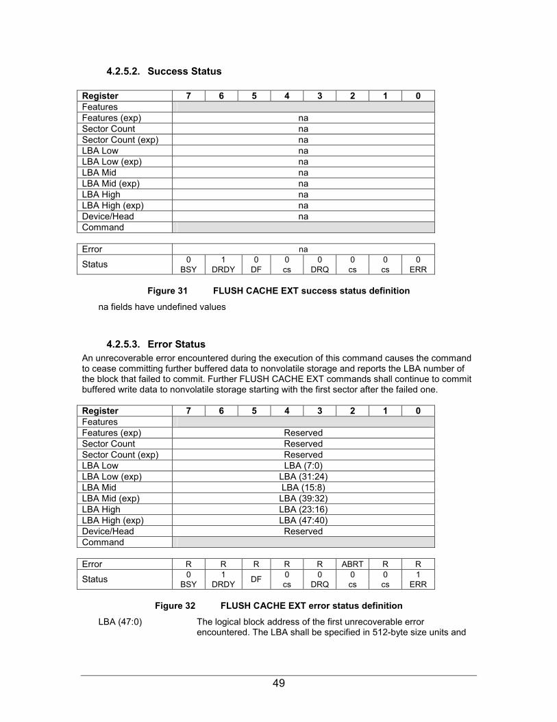
49
4.2.5.2. Success Status Register 7 6 5 4 3 2 1 0 Features Features (exp) na Sector Count na Sector Count (exp) na LBA Low na LBA Low (exp) na LBA Mid na LBA Mid (exp) na LBA High na LBA High (exp) na Device/Head na Command
Error na 0 1 0 0 0 0 0 0Status BSY DRDY DF cs DRQ cs cs ERR
Figure 31 FLUSH CACHE EXT success status definition
na fields have undefined values
4.2.5.3. Error Status An unrecoverable error encountered during the execution of this command causes the command to cease committing further buffered data to nonvolatile storage and reports the LBA number of the block that failed to commit. Further FLUSH CACHE EXT commands shall continue to commit buffered write data to nonvolatile storage starting with the first sector after the failed one. Register 7 6 5 4 3 2 1 0 Features Features (exp) Reserved Sector Count Reserved Sector Count (exp) Reserved LBA Low LBA (7:0) LBA Low (exp) LBA (31:24) LBA Mid LBA (15:8) LBA Mid (exp) LBA (39:32) LBA High LBA (23:16) LBA High (exp) LBA (47:40) Device/Head Reserved Command
Error R R R R R ABRT R R 0 1 0 0 0 0 1Status BSY DRDY DF cs DRQ cs cs ERR
Figure 32 FLUSH CACHE EXT error status definition
LBA (47:0) The logical block address of the first unrecoverable error encountered. The LBA shall be specified in 512-byte size units and
50
shall be constrained based on the value in Word 106 of IDENTIFY DEVICE.
DF DF (Device Fault) shall be set to one if a device fault has occurred. ABRT Set to one. Reserved Reserved fields shall be cleared to zero (0).
51
5. Status and Control Registers The following section defines the Status and Control Registers (SCRs) and their functions. The protocol for accessing the Status and Control Registers is defined in Section 2. Figure 33 shows how the MMC register space is allocated.
CMD60 access
only
0h
80h
Status and Control
Registers
MMC Register Space
ATA Taskfile Registers
CMD39 or
CMD60 access
FFh
10h
Figure 33 MMC Register Space
5.1. Access Primitives There are only two operations that can be performed on the Status and Control Registers – reading a register and writing a register. The functions performed by the registers in response to being read/written are defined in the following sections. The Status and Control Registers are accessed using the RW_MULTIPLE_REGISTER (CMD60) command.
5.1.1. Register Read Reading undefined register address returns an indeterminate value. The Register Read operation has no error conditions. The protocol definition for the Register Read function is defined in Section 2.
52
5.1.2. Register Write Writing undefined or unsupported registers shall have no effect. The Register Write operation has no error conditions. The protocol definition for the Register Write function is defined in Section 2.
5.2. Register Definition All registers are 32 bits in size and no partial access to the registers is accommodated. A read of a Status and Control register shall provide a self-consistent image of that register. Registers that only define a few bits shall return zeroes for the unused/undefined bits. The Status and Control registers start at MMC register address 80h. All register access shall be Dword aligned and for one or more Dwords in length. Bit 31 of each register indicates whether that register is supported. Bit 30 of each register indicates whether the value in bits 29-0 in a supported register is valid. For values that are persistent across power cycles, the valid bit in the register may not be asserted until device spin-up has occurred if the persistent values are stored on the media. Figure 34 lists the defined registers. The functions provided by the internal registers are intended to expose information on the operating conditions of the device to permit hosts to provide services similar to those provided by SMART. Hosts may also utilize the internal register data to control the operation of the device. For example, hosts may elect to not attempt to spin-up a device if the environmental conditions are not favorable due to extreme heat or cold. Register
Index Byte
Address Register Name M/O R/W Description
0 80h scrTempC O RO Current temperature reading 1 84h scrTempMaxP O RO Peak maximum temperature
reading 2 88h scrTempMinP O RO Peak minimum temperature
reading 3 8Ch scrStatus O RO Status information for the
device 4 90h scrReallocsA O RO Accumulated number of
reallocated ATA sectors 5 94h scrERetractsA O RO Accumulated number of
uncontrolled retracts 6 98h scrCapabilities M RO Capabilities and features of
device 7-15 9Ch – BFh Reserved na RO Reserved for future definition 16 C0h scrControl M RW Control capabilities of device
17-23 C4h – DFh Reserved na RW Reserved for future definition 24-31 E0h – FFh Vendor Specific na RW Vendor specific registers
Key: M/O = Mandatory/optional requirement. M = Support of the register is mandatory. O = Support of the register is optional. R/W = Read/write support. RO = The register is read-only. RW = The register may be read or written.
Figure 34 Status and Control Register Map
53
5.2.1. scrTempC Register The scrTempC register holds the current temperature value of the device. The rate at which the device updates the temperature value is vendor specific. The resolution of the temperature value is vendor specific. Bits 15-0 is a two’s complement value of the number of degrees Celsius. Bits 29-16 are reserved. Bit 30 if set to one indicates that the values in bits 29-0 are valid. Bit 30 if cleared to zero indicates that the values in bits 29-0 are not valid and should not be used. Bit 31 if set to one indicates that the register is supported by the device. Bit 31 if cleared to zero indicates that the register is not supported by the device. When bit 31 is cleared to zero, bits 30-0 have indeterminate values. This register is not affected by reception of the MMC command GO_IDLE_STATE (CMD0) or by an ATA software reset.
5.2.2. scrTempMaxP Register The scrTempMaxP register holds the latched peak maximum temperature value of the device. Reading the register returns the highest temperature value the device has registered. The device shall update the register with a new value if the present temperature indication is greater than the value held in the register. The rate at which the device updates the maximum latched temperature value is vendor specific and the means by which the device determines the maximum temperature encountered is vendor specific. The resolution of the maximum temperature value is vendor specific. Bits 15-0 is a two’s complement value of the number of degrees Celsius. This value shall be persistent across power cycles. Bits 29-16 are reserved. Bit 30 if set to one indicates that the values in bits 29-0 are valid. Bit 30 if cleared to zero indicates that the values in bits 29-0 are not valid and should not be used. Bit 31 if set to one indicates that the register is supported by the device. Bit 31 if cleared to zero indicates that the register is not supported by the device. When bit 31 is cleared to zero, bits 30-0 have indeterminate values. This register is not affected by reception of the MMC command GO_IDLE_STATE (CMD0) or by an ATA software reset.
5.2.3. scrTempMinP Register The scrTempMinP register holds the latched peak minimum temperature value of the device. Reading the register returns the lowest temperature value the device has registered. The device shall update the register with a new value if the present temperature indication is lower than the value held in the register. The rate at which the device updates the minimum latched temperature value is vendor specific and the means by which the device determines the minimum temperature encountered is vendor specific. The resolution of the minimum temperature value is vendor specific.
54
Bits 15-0 is a two’s complement value of the number of degrees Celsius. This value shall be persistent across power cycles. Bits 29-16 are reserved. Bit 30 if set to one indicates that the values in bits 29-0 are valid. Bit 30 if cleared to zero indicates that the values in bits 29-0 are not valid and should not be used. Bit 31 if set to one indicates that the register is supported by the device. Bit 31 if cleared to zero indicates that the register is not supported by the device. When bit 31 is cleared to zero, bits 30-0 have indeterminate values. This register is not affected by reception of the MMC command GO_IDLE_STATE (CMD0) or by an ATA software reset.
5.2.4. scrStatus Register The scrStatus register specifies status information for the operation of the device. Bit 0 is read-only. Bit 0 when set to one indicates that the device has experienced excessive abuse due to shock or other handling. Bit 0 when cleared to zero indicates that the device has not experienced excessive abuse as measured by the device. The method for determining when to set this bit is vendor specific. This value shall be persistent across power cycles. Bits 29-1 are reserved. Bit 30 if set to one indicates that the values in bits 29-0 are valid. Bit 30 if cleared to zero indicates that the values in bits 29-0 are not valid and should not be used. Bit 31 if set to one indicates that the register is supported by the device. Bit 31 if cleared to zero indicates that the register is not supported by the device. When bit 31 is cleared to zero, bits 30-0 have indeterminate values. This register is not affected by reception of the MMC command GO_IDLE_STATE (CMD0) or by an ATA software reset.
5.2.5. scrReAllocsA Register The scrReAllocsA register holds the accumulated number of CE-ATA sector reallocations performed, including reallocations that occur due to read or write operations. A reallocation is when a portion of a CE-ATA sector is moved from a bad location to a spare location. The ReAllocsA register provides an indication to host software of the number of grown defects that have been discovered over the life of the device. Bits 29-0 holds the accumulated number of CE-ATA sector reallocations performed over the life of the device. This value shall be persistent across power cycles. Bit 30 if set to one indicates that the values in bits 29-0 are valid. Bit 30 if cleared to zero indicates that the values in bits 29-0 are not valid and should not be used. Bit 31 if set to one indicates that the register is supported by the device. Bit 31 if cleared to zero indicates that the register is not supported by the device. When bit 31 is cleared to zero, bits 30-0 have indeterminate values.
55
This register is not affected by reception of the MMC command GO_IDLE_STATE (CMD0) or by an ATA software reset.
5.2.6. scrERetractsA Register The scrERetractsA register holds the accumulated number of uncontrolled retracts over the life of the device. A retract is an unloading of the head from the disk. This register is only supported by devices that have rotating media. Support for this register is optional, but devices that do support it shall ensure the value is persistent across all event types including power cycles. Bits 29-0 holds the accumulated number of uncontrolled retracts performed over the life of the device. This value shall be persistent across power cycles. Bit 30 if set to one indicates that the values in bits 29-0 are valid. Bit 30 if cleared to zero indicates that the values in bits 29-0 are not valid and should not be used. Bit 31 if set to one indicates that the register is supported by the device. Bit 31 if cleared to zero indicates that the register is not supported by the device. When bit 31 is cleared to zero, bits 30-0 have indeterminate values. This register is not affected by reception of the MMC command GO_IDLE_STATE (CMD0) or by an ATA software reset.
5.2.7. scrCapabilities The scrCapabilities register specifies the capabilities and features of the device. Bit 0 is read-only and shall be set to one. Bit 0 indicates that the device supports an MMC data block size of 512 bytes. Bit 1 is read-only. Bit 1 if set to one indicates that the device supports an MMC data block size of 1KB. Bit 1 if cleared to zero indicates that the device does not support an MMC data block size of 1KB. Bit 2 is read-only. Bit 2 if set to one indicates that the device supports an MMC data block size of 4KB. Bit 2 if cleared to zero indicates that the device does not support an MMC data block size of 4KB. Bits 29-3 are reserved. Bit 30 if set to one indicates that the values in bits 29-0 are valid. Bit 30 if cleared to zero indicates that the values in bits 29-0 are not valid and should not be used. Bit 31 if set to one indicates that the register is supported by the device. Bit 31 if cleared to zero indicates that the register is not supported by the device. When bit 31 is cleared to zero, bits 30-0 have indeterminate values. This register is not affected by reception of the MMC command GO_IDLE_STATE (CMD0) or by an ATA software reset.
5.2.8. scrControl The scrControl register is used to control the operation of the device.
56
Bits 1-0 control the MMC data block size. The MMC data block size is encoded as follows: 00b – MMC data block size is 512 bytes 01b – MMC data block size is 1KB 10b – MMC data block size is 4KB 11b – Reserved By default, this field is 00b corresponding to an MMC data block size of 512 bytes. The host shall only set the MMC data block size to a value that the device supports as specified in the scrCapabilities register. Bits 29-2 are reserved. Bit 30 if set to one indicates that the values in bits 29-0 are valid. Bit 30 if cleared to zero indicates that the values in bits 29-0 are not valid and should not be used. Bit 31 if set to one indicates that the register is supported by the device. Bit 31 if cleared to zero indicates that the register is not supported by the device. When bit 31 is cleared to zero, bits 30-0 have indeterminate values. When MMC command GO_IDLE_STATE (CMD0) is received, this register shall be reset to its default values. This register is not affected by reception of an ATA software reset.
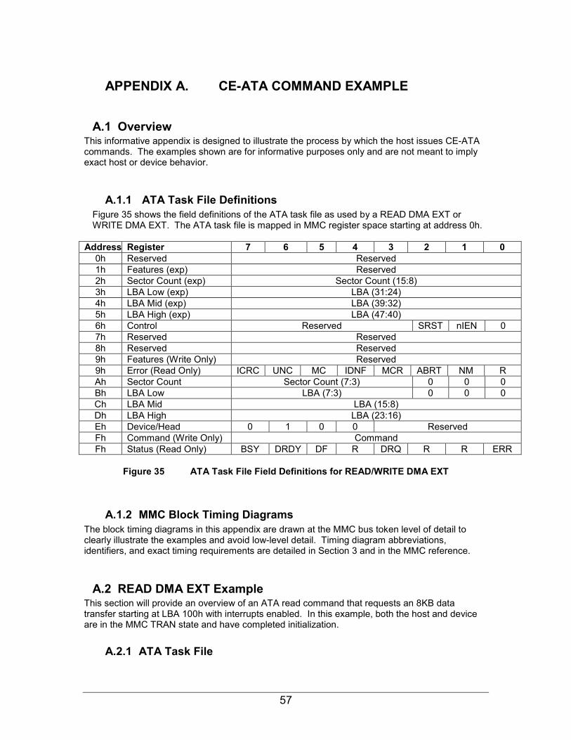
57
APPENDIX A. CE-ATA COMMAND EXAMPLE
A.1 Overview This informative appendix is designed to illustrate the process by which the host issues CE-ATA commands. The examples shown are for informative purposes only and are not meant to imply exact host or device behavior.
A.1.1 ATA Task File Definitions Figure 35 shows the field definitions of the ATA task file as used by a READ DMA EXT or WRITE DMA EXT. The ATA task file is mapped in MMC register space starting at address 0h.
Address Register 7 6 5 4 3 2 1 0 0h Reserved Reserved 1h Features (exp) Reserved 2h Sector Count (exp) Sector Count (15:8) 3h LBA Low (exp) LBA (31:24) 4h LBA Mid (exp) LBA (39:32) 5h LBA High (exp) LBA (47:40) 6h Control Reserved SRST nIEN 0 7h Reserved Reserved 8h Reserved Reserved 9h Features (Write Only) Reserved 9h Error (Read Only) ICRC UNC MC IDNF MCR ABRT NM R Ah Sector Count Sector Count (7:3) 0 0 0 Bh LBA Low LBA (7:3) 0 0 0 Ch LBA Mid LBA (15:8) Dh LBA High LBA (23:16) Eh Device/Head 0 1 0 0 Reserved Fh Command (Write Only) Command Fh Status (Read Only) BSY DRDY DF R DRQ R R ERR
Figure 35 ATA Task File Field Definitions for READ/WRITE DMA EXT
A.1.2 MMC Block Timing Diagrams The block timing diagrams in this appendix are drawn at the MMC bus token level of detail to clearly illustrate the examples and avoid low-level detail. Timing diagram abbreviations, identifiers, and exact timing requirements are detailed in Section 3 and in the MMC reference.
A.2 READ DMA EXT Example This section will provide an overview of an ATA read command that requests an 8KB data transfer starting at LBA 100h with interrupts enabled. In this example, both the host and device are in the MMC TRAN state and have completed initialization.
A.2.1 ATA Task File
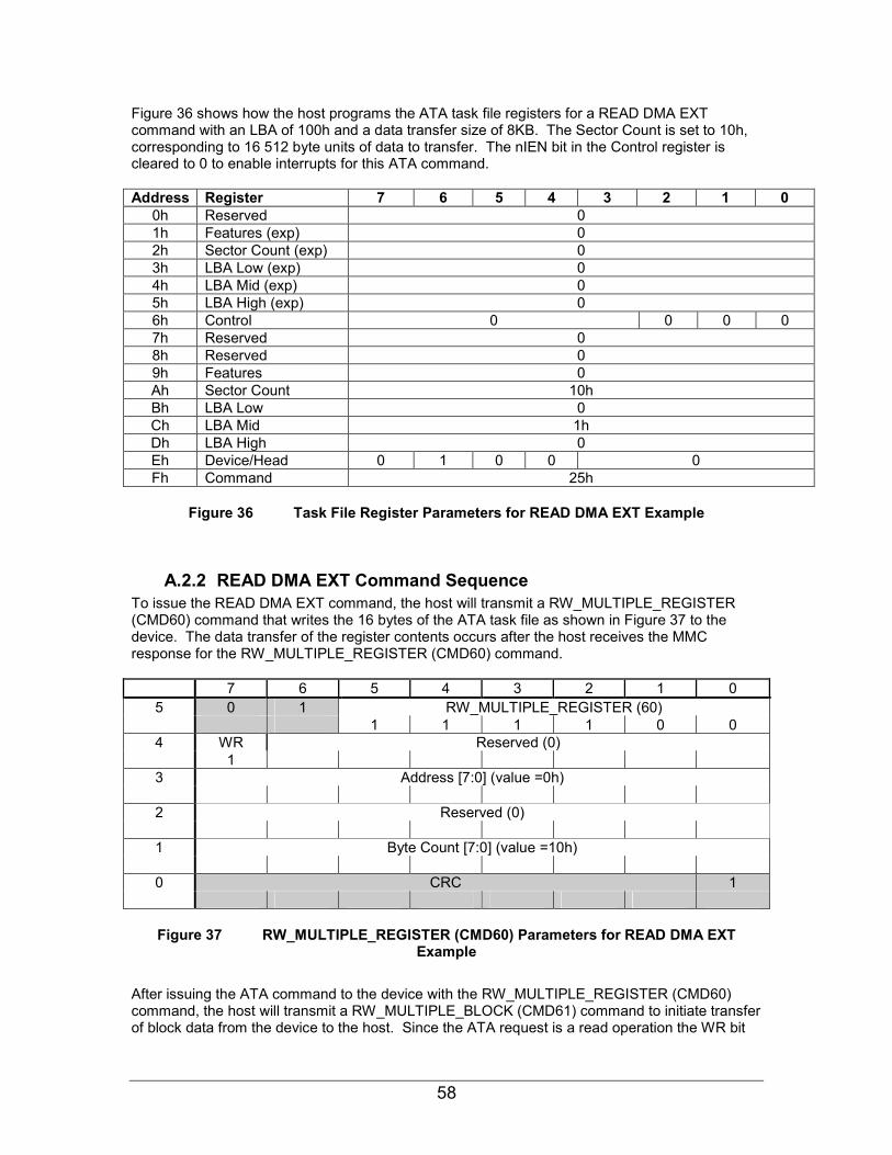
58
Figure 36 shows how the host programs the ATA task file registers for a READ DMA EXT command with an LBA of 100h and a data transfer size of 8KB. The Sector Count is set to 10h, corresponding to 16 512 byte units of data to transfer. The nIEN bit in the Control register is cleared to 0 to enable interrupts for this ATA command. Address Register 7 6 5 4 3 2 1 0
0h Reserved 0 1h Features (exp) 0 2h Sector Count (exp) 0 3h LBA Low (exp) 0 4h LBA Mid (exp) 0 5h LBA High (exp) 0 6h Control 0 0 0 0 7h Reserved 0 8h Reserved 0 9h Features 0 Ah Sector Count 10h Bh LBA Low 0 Ch LBA Mid 1h Dh LBA High 0 Eh Device/Head 0 1 0 0 0 Fh Command 25h
Figure 36 Task File Register Parameters for READ DMA EXT Example
A.2.2 READ DMA EXT Command Sequence To issue the READ DMA EXT command, the host will transmit a RW_MULTIPLE_REGISTER (CMD60) command that writes the 16 bytes of the ATA task file as shown in Figure 37 to the device. The data transfer of the register contents occurs after the host receives the MMC response for the RW_MULTIPLE_REGISTER (CMD60) command.
7 6 5 4 3 2 1 00 1 RW_MULTIPLE_REGISTER (60) 5
1 1 1 1 0 0WR Reserved (0) 4
1Address [7:0] (value =0h) 3
Reserved (0) 2
Byte Count [7:0] (value =10h) 1
CRC 10
Figure 37 RW_MULTIPLE_REGISTER (CMD60) Parameters for READ DMA EXT Example
After issuing the ATA command to the device with the RW_MULTIPLE_REGISTER (CMD60) command, the host will transmit a RW_MULTIPLE_BLOCK (CMD61) command to initiate transfer of block data from the device to the host. Since the ATA request is a read operation the WR bit
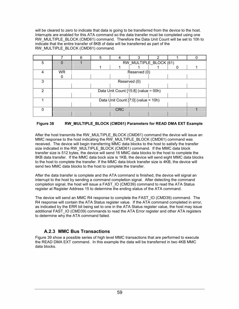
59
will be cleared to zero to indicate that data is going to be transferred from the device to the host. Interrupts are enabled for this ATA command so the data transfer must be completed using one RW_MULTIPLE_BLOCK (CMD61) command. Therefore the Data Unit Count will be set to 10h to indicate that the entire transfer of 8KB of data will be transferred as part of the RW_MULTIPLE_BLOCK (CMD61) command.
7 6 5 4 3 2 1 00 1 RW_MULTIPLE_BLOCK (61) 5
1 1 1 1 0 1WR Reserved (0) 4
0Reserved (0) 3
Data Unit Count [15:8] (value = 00h) 2
Data Unit Count [7:0] (value = 10h) 1
CRC 10
Figure 38 RW_MULTIPLE_BLOCK (CMD61) Parameters for READ DMA EXT Example
After the host transmits the RW_MULTIPLE_BLOCK (CMD61) command the device will issue an MMC response to the host indicating the RW_MULTIPLE_BLOCK (CMD61) command was received. The device will begin transferring MMC data blocks to the host to satisfy the transfer size indicated in the RW_MULTIPLE_BLOCK (CMD61) command. If the MMC data block transfer size is 512 bytes, the device will send 16 MMC data blocks to the host to complete the 8KB data transfer. If the MMC data bock size is 1KB, the device will send eight MMC data blocks to the host to complete the transfer. If the MMC data block transfer size is 4KB, the device will send two MMC data blocks to the host to complete the transfer. After the data transfer is complete and the ATA command is finished, the device will signal an interrupt to the host by sending a command completion signal. After detecting the command completion signal, the host will issue a FAST_IO (CMD39) command to read the ATA Status register at Register Address 15 to determine the ending status of the ATA command. The device will send an MMC R4 response to complete the FAST_IO (CMD39) command. The R4 response will contain the ATA Status register value. If the ATA command completed in error, as indicated by the ERR bit being set to one in the ATA Status register value, the host may issue additional FAST_IO (CMD39) commands to read the ATA Error register and other ATA registers to determine why the ATA command failed.
A.2.3 MMC Bus Transactions Figure 39 show a possible series of high level MMC transactions that are performed to execute the READ DMA EXT command. In this example the data will be transferred in two 4KB MMC data blocks.
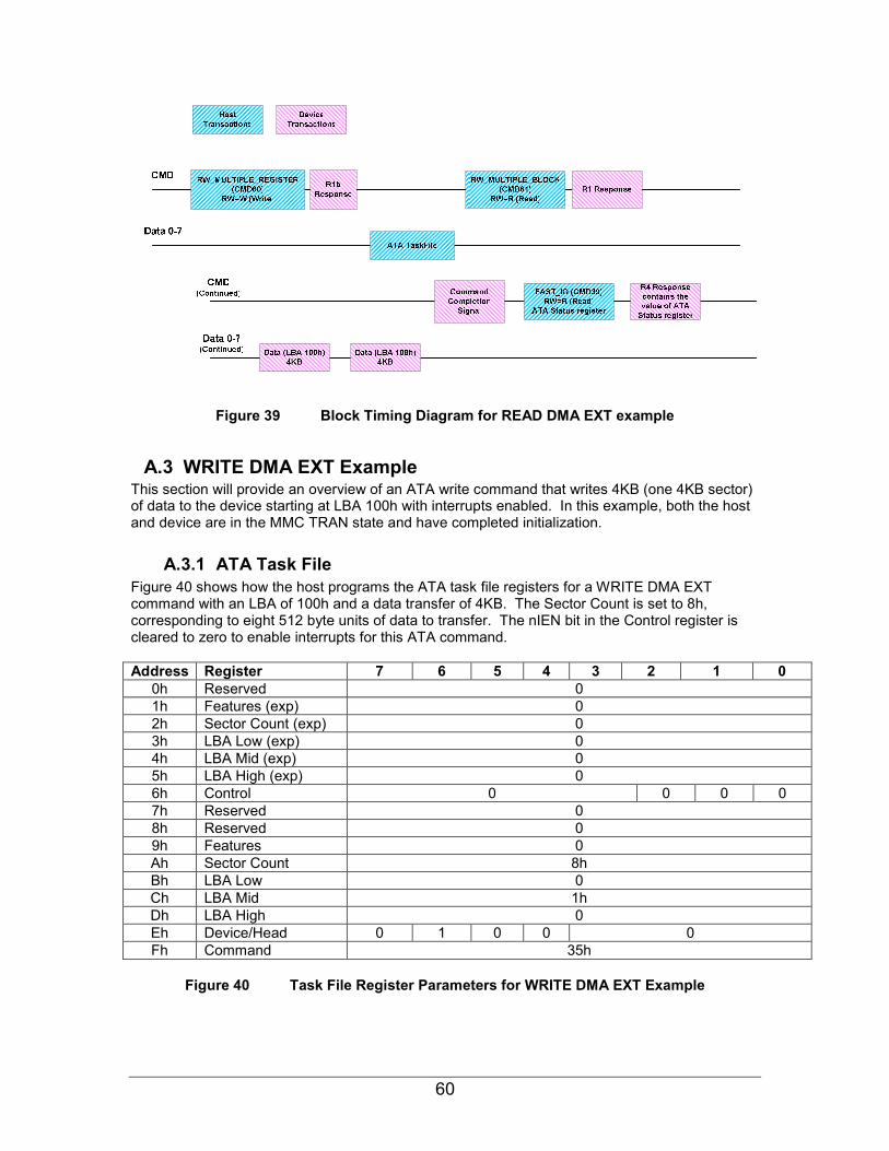
60
Figure 39 Block Timing Diagram for READ DMA EXT example
A.3 WRITE DMA EXT Example This section will provide an overview of an ATA write command that writes 4KB (one 4KB sector) of data to the device starting at LBA 100h with interrupts enabled. In this example, both the host and device are in the MMC TRAN state and have completed initialization.
A.3.1 ATA Task File Figure 40 shows how the host programs the ATA task file registers for a WRITE DMA EXT command with an LBA of 100h and a data transfer of 4KB. The Sector Count is set to 8h, corresponding to eight 512 byte units of data to transfer. The nIEN bit in the Control register is cleared to zero to enable interrupts for this ATA command. Address Register 7 6 5 4 3 2 1 0
0h Reserved 0 1h Features (exp) 0 2h Sector Count (exp) 0 3h LBA Low (exp) 0 4h LBA Mid (exp) 0 5h LBA High (exp) 0 6h Control 0 0 0 0 7h Reserved 0 8h Reserved 0 9h Features 0 Ah Sector Count 8h Bh LBA Low 0 Ch LBA Mid 1h Dh LBA High 0 Eh Device/Head 0 1 0 0 0 Fh Command 35h
Figure 40 Task File Register Parameters for WRITE DMA EXT Example
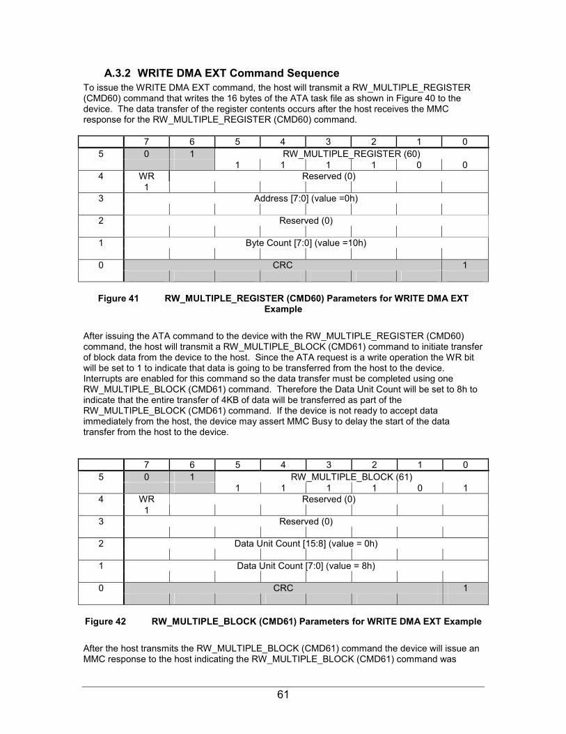
61
A.3.2 WRITE DMA EXT Command Sequence To issue the WRITE DMA EXT command, the host will transmit a RW_MULTIPLE_REGISTER (CMD60) command that writes the 16 bytes of the ATA task file as shown in Figure 40 to the device. The data transfer of the register contents occurs after the host receives the MMC response for the RW_MULTIPLE_REGISTER (CMD60) command.
7 6 5 4 3 2 1 00 1 RW_MULTIPLE_REGISTER (60) 5
1 1 1 1 0 0WR Reserved (0) 4
1Address [7:0] (value =0h) 3
Reserved (0) 2
Byte Count [7:0] (value =10h) 1
CRC 10
Figure 41 RW_MULTIPLE_REGISTER (CMD60) Parameters for WRITE DMA EXT Example
After issuing the ATA command to the device with the RW_MULTIPLE_REGISTER (CMD60) command, the host will transmit a RW_MULTIPLE_BLOCK (CMD61) command to initiate transfer of block data from the device to the host. Since the ATA request is a write operation the WR bit will be set to 1 to indicate that data is going to be transferred from the host to the device. Interrupts are enabled for this command so the data transfer must be completed using one RW_MULTIPLE_BLOCK (CMD61) command. Therefore the Data Unit Count will be set to 8h to indicate that the entire transfer of 4KB of data will be transferred as part of the RW_MULTIPLE_BLOCK (CMD61) command. If the device is not ready to accept data immediately from the host, the device may assert MMC Busy to delay the start of the data transfer from the host to the device.
7 6 5 4 3 2 1 00 1 RW_MULTIPLE_BLOCK (61) 5
1 1 1 1 0 1WR Reserved (0) 4
1Reserved (0) 3
Data Unit Count [15:8] (value = 0h) 2
Data Unit Count [7:0] (value = 8h) 1
CRC 10
Figure 42 RW_MULTIPLE_BLOCK (CMD61) Parameters for WRITE DMA EXT Example
After the host transmits the RW_MULTIPLE_BLOCK (CMD61) command the device will issue an MMC response to the host indicating the RW_MULTIPLE_BLOCK (CMD61) command was
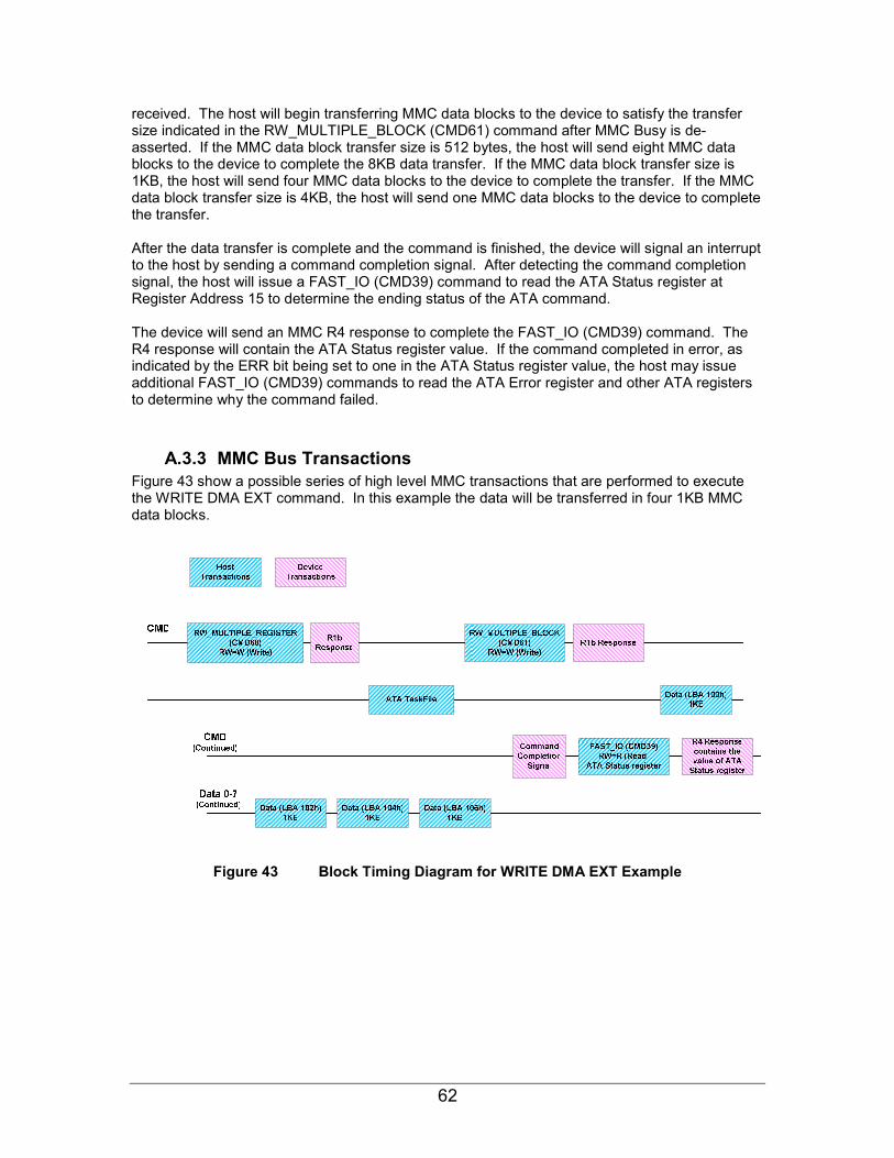
62
received. The host will begin transferring MMC data blocks to the device to satisfy the transfer size indicated in the RW_MULTIPLE_BLOCK (CMD61) command after MMC Busy is de-asserted. If the MMC data block transfer size is 512 bytes, the host will send eight MMC data blocks to the device to complete the 8KB data transfer. If the MMC data block transfer size is 1KB, the host will send four MMC data blocks to the device to complete the transfer. If the MMC data block transfer size is 4KB, the host will send one MMC data blocks to the device to complete the transfer. After the data transfer is complete and the command is finished, the device will signal an interrupt to the host by sending a command completion signal. After detecting the command completion signal, the host will issue a FAST_IO (CMD39) command to read the ATA Status register at Register Address 15 to determine the ending status of the ATA command. The device will send an MMC R4 response to complete the FAST_IO (CMD39) command. The R4 response will contain the ATA Status register value. If the command completed in error, as indicated by the ERR bit being set to one in the ATA Status register value, the host may issue additional FAST_IO (CMD39) commands to read the ATA Error register and other ATA registers to determine why the command failed.
A.3.3 MMC Bus Transactions Figure 43 show a possible series of high level MMC transactions that are performed to execute the WRITE DMA EXT command. In this example the data will be transferred in four 1KB MMC data blocks.
Figure 43 Block Timing Diagram for WRITE DMA EXT Example