cdb8427 evaluation board for cs8427 zreceives and transmits aes/ebu, s/pdif and eiaj-340 compatible...
TRANSCRIPT

Preliminary Product Information This document conCirrus Logic reserv
Copyrig(
Cirrus Logic, Inc.P.O. Box 17847, Austin, Texas 78760(512) 445 7222 FAX: (512) 445 7581http://www.cirrus.com
CDB8427
Evaluation Board for CS8427
FeaturesReceives and transmits AES/EBU, S/PDIF and EIAJ-340 compatible digital audioConvenient access to the Serial Audio Input Port and Serial Audio Output Port through headers.Runs from a single 5 Volt supply.Crystal supplied to allow operation at 48 kHz, sample rate.Digital patch area.
DescriptionThe CDB8427 is designed to allow rapid evaluation ofthe CS8427. The board is set up for easy connection toan Audio Precision or a Rohde and Schwarz test system.
Input and output data formats may independently be setto either AES/EBU, or S/PDIF with either optical or coax-ial physical format.
Separate headers are provided so the Serial Audio InputPort and Serial Audio Output Port may be interfaced tooff board circuits.
Microsoft® Windows® 98 PC software provides a GUIinterface to make configuration easy. The software com-municates through the PC’s RS232 port to amicrocontroller on the evaluation board that controls theCS8427. All the possible software modes of the CS8427may be tested.
ORDERING INFORMATIONCDB8427 Evaluation Board
I
CS8427
A m te lµ C
O ptica l In
S /P D IF In
A E S 3 In A E S 3 O u t
S /P D IF O u t
O ptica l O u t
R S 232 port to P C
tains information for a new product.es the right to modify this product without notice.
1
ht Cirrus Logic, Inc. 2002All Rights Reserved)
AUG ‘02DS477DB2

CDB8427
TABLE OF CONTENTS1. OVERVIEW ............................................................................................................................... 3
1.1 CS8427 .............................................................................................................................. 31.2 Microcontroller and Memory .............................................................................................. 31.3 Crystal Oscillators .............................................................................................................. 31.4 RS232 Port ........................................................................................................................ 31.5 LED Function Indicators ..................................................................................................... 3
2. CDB8427.EXE QUICK START GUIDE .................................................................................... 42.1 Setting up the Hardware .................................................................................................... 42.2 Installing the Software ........................................................................................................ 42.3 Starting up the Software .................................................................................................... 42.4 Starting up the Hardware ................................................................................................... 4
3. CDB8427.EXE USER'S GUIDE ................................................................................................ 63.1 Main Window ..................................................................................................................... 63.2 Board Setup ....................................................................................................................... 73.3 Script file syntax ................................................................................................................. 7
LIST OF FIGURESFigure 1. CDB8427 Control Panel Main Window ............................................................................ 6Figure 2. Board Setup Panel ........................................................................................................... 7Figure 3. CS8427 Digital Audio Transceiver ................................................................................... 9Figure 4. Atmel AVR RISC Microcontroller ................................................................................... 10Figure 5. Power Supplies and Reset Circuit.................................................................................. 11Figure 6. Silkscreen....................................................................................................................... 12Figure 7. Top PCB......................................................................................................................... 13Figure 8. Bottom PCB ................................................................................................................... 14
LIST OF TABLESTable 1. System Connections ......................................................................................................... 5Table 2. CDB8427 Jumper Settings................................................................................................ 5Table 3. Script file syntax description.............................................................................................. 7
Contacting Cirrus Logic SupportFor a com plete lis ting o f D irect Sales, D istributor, and Sales R epresentative contacts, visit the C irrus Logic w eb site at:http://www.cirrus.com/corporate/contacts/sales.cfm
IM PO RTANT NO TICE
“Pre lim inary” p roduct in form ation describes products tha t are in production, but for wh ich full characterization data is not yet ava ilable. “Advance” product infor-m ation describes products tha t a re in developm ent and subject to developm ent changes. C irrus Logic, Inc. and its subsidiaries (“C irrus”) believe that the infor-m ation contained in th is docum ent is accurate and reliable. However, the inform ation is subject to change w ithout notice and is provided “AS IS” w ithout warrantyof any kind (express or im plied). Custom ers are advised to obta in the latest version o f relevant inform ation to verify, before placing orders, tha t in form ation beingre lied on is current and com ple te. A ll products are sold subject to the term s and conditions of sale supplied a t the tim e of order acknow ledgm ent, including thosepertaining to warranty, patent infringem ent, and lim itation of liability. No responsibility is assum ed by C irrus fo r the use of th is inform ation, including use of thisinform ation as the basis for m anufacture or sale of any item s, or fo r infringem ent of patents or other righ ts of third parties. This docum ent is the property o f C irrusand by furnishing this inform ation , C irrus grants no license, express or im p lied under any patents, m ask work rights, copyrights, tradem arks, trade secrets orother inte llectual property rights. C irrus owns the copyrights o f the in form ation contained here in and gives consent for copies to be m ade of the inform ation onlyfor use w ithin your organization w ith respect to C irrus integrated circuits or other parts of C irrus. This consent does not extend to other copying such as copyingfor general d istribution , advertising or prom otional purposes, or for creating any work for resale.
An export perm it needs to be obtained from the com petent authorities of the Japanese G overnm ent if any of the products or techno logies described in this m a-terial and contro lled under the “Foreign Exchange and Foreign Trade Law” is to be exported or taken out o f Japan. An export license and/or quota needs to beobtained from the com petent au thorities of the Chinese G overnm ent if any of the products or technolog ies described in this m aterial is sub ject to the PRC ForeignTrade Law and is to be exported or taken out of the PRC.
CERTAIN APPLICATIO NS USING SEM ICO NDUCTO R PRO DUCTS M AY INVO LVE PO TENTIAL R ISKS O F DEATH, PERSO NAL INJURY, O R SEVEREPRO PERTY O R ENVIRO NM ENTAL DAM AG E (“CRITICAL APPLICATIO NS”). C IRRUS PRO DUCTS ARE NO T DESIG NED, AUTHO RIZED, O R W ARRANT-ED TO BE SUITABLE FO R USE IN L IFE-SUPPO RT DEVICES O R SYSTEM S O R O THER CRITICAL APPLICATIO NS. INCLUSIO N O F C IRRUS PRO DUCTSIN SUCH APPLICATIO NS IS UNDERSTO O D TO BE FULLY AT THE CUSTO M ER'S R ISK.
C irrus Logic, C irrus, and the C irrus Logic logo designs are tradem arks of C irrus Logic, Inc. A ll other brand and product nam es in this docum ent m ay be trade-m arks or service m arks o f their respective owners.
2
CDB8427
1. OVERVIEW
The CDB8427 evaluation board contains a CS8427and the supporting circuitry necessary for it to op-erate. The input and output options include AES3and S/PDIF in optical and coaxial formats. In soft-ware mode, the control registers of the CS8427 areset by an Atmel AVR RISC microcontroller. A Mi-crosoft Windows 98 based program communicateswith the micro through an RS232 port to control theconfiguration.
1.1 CS8427
The features and functions of the CS8427 are de-scribed in its data sheet.
1.2 Microcontroller and Memory
The functions of the board are controlled by an At-mel AVR RISC microcontroller. The board isequipped with 512 KBytes of static RAM so thatChannel Status and User bits from the AES streammay be captured and uploaded to the host PC. Themicrocontroller communicates with the CS8427through its SPI port. The Atmel AVR RISC micro-controller may be bypassed in order to utilize anexternal microcontroller through header J10. Head-er J9 allows the microcontroller on the board to beprogrammed with the programmer that is suppliedin the Atmel STK-300 development kit. Additionalsoftware development tools and applications infor-mation for the Atmel microcontroller are availableat: http://www.atmel.com.
1.3 Crystal Oscillators
There are positions for two crystal oscillators onthe board. Both locations are equipped with pinsockets that allow the oscillators to be removed.The oscillator labeled U10 provides the 6 MHzclock for the microcontroller and should not bechanged unless you plan on reprogramming the mi-cro.
U3 is the oscillator that provides the Output MasterClock for the CS8427. The board is shipped with a12.288 MHz crystal oscillator that can be stuffed atU3 to set the output sampling rate to 48 kHz.
1.4 RS232 Port
The RS232 port on the upper right hand side of theboard should be connected to the serial port of thePC running the CDB8427 control software. Followthe software instructions to properly configure theserial port for use with the evaluation board.
1.5 LED Function Indicators
LEDs D8 and D9 on the upper right hand corner ofthe board allow the user to determine when data isbeing transmitted over the RS232 link. The redLED D4 is the reset indicator and the red LED D1is connected to the RERR pin of the CS8427. Thetwo remaining LEDs on the board are not currentlyof use to the end user
3

CDB8427
2. CDB8427.EXE QUICK START GUIDE
2.1 Setting up the HardwareNote: SeeTable 1 on page 5 and Table 2 on page 5 for
the configuration and jumper settings.
1) Connect the CDB8427 to a 5 V DC power sup-ply.
2) Set: J11 to Optical, J16 to S/PDIF, enable J13(S/PDIF), and disable J15 (MUTE).
3) Connect the CDB8427 to the PC COM port us-ing RS232 cable.
4) Apply power to the board.
5) Press the RESET switch (S5).
At this point, the RERR and PROC should be lit.The hardware is now ready!
2.2 Installing the Software
1) Create a directory called CDB8427 anywhereon your system.
2) Copy CDB8427.exe into this directory.
3) If you do not already have them, copy the in-cluded DLLs msvcrt.dll and mfc42.dll intoyour \Windows\System directory.
4) If desired, create a shortcut to CDB8427.exe onyour desktop.
At this point, you are ready to start up the software.
2.3 Starting up the Software
1) Double-click on CDB8427.exe or its short-cut.
2) If you get errors right away, the COM portneeds to be set properly.
3) Click anywhere but inside one of the boxes, thisbrings up the Board Setup control panel.
4) Select the COM port you are using to connectto the CDB8427.
5) Shut down the application, reset the board, andthen restart the application.
2.4 Starting up the Hardware
1) Click anywhere but inside one of the boxes, thisbrings up the Board Setup control panel.
2) Click on the Reset button. You should see theTX and RX leds light up briefly.
3) Click on the AES3 Transmitter tab, then set theTransmitter data source to AES3 Receiver.
4) Click on the Clock Sources tab, click onRMCK derived from AES3 input frame and un-check the Stop Internal Clocks box.
5) Check the performance of the board by doingan FFT with a -1dBFS 1kHz sine wave for in-put at 44.1kHz and 48kHz sample rates usingthe optical input and optical output.
.
4

CDB8427
CONNECTOR INPUT/OUTPUT SIGNAL PRESENT+5V Input +5 Volt powerGND Input Ground connection from power supply
OPTICAL INPUT Input Digital Audio Interface optical inputS/PDIF INPUT Input Digital Audio Interface coaxial inputAES3 INPUT Input Digital Audio Interface XLR input
RS232 Input/Output Parallel RS232 port for connection to serial port of PCOPTICAL OUTPUT Output Digital Audio Interface optical output (always enabled)S/PDIF OUTPUT Output Digital Audio Interface coaxial outputAES3 OUTPUT Output Digital Audio Interface XLR output
J5 Input/Output I/O for RMCLK, ISCLK,ILRCK, and SDINJ6 Input/Output I/O for OLRCK, OSCLK, OMCK, and SDOUTJ9 Input 10-pin header for external programming of Atmel AVR µCJ10 Input/Output 12-pin header for CS8427 control from external µC
Table 1. System Connections
JUMPER PURPOSE POSITION FUNCTION SELECTEDJ11 Selects physical format of digital
audio interface input AES3 & S/PDIF
OPTICALConnects input as either AES3 or S/PDIF Connects input as OPTICAL
J12 Configures AES3 INPUT ENABLEDISABLE
AES3 INPUT enabled AES3 INPUT disabled
J13 Configures S/PDIF INPUT ENABLEDISABLE
S/PDIF INPUT enabled S/PDIF INPUT disabled
J14 Configures OPTICAL INPUT ENABLEDISABLE
OPTICAL INPUT enabled OPTICAL INPUT disabled
J16 Selects physical format of digital audio interface output
AES3S/PDIF
Connects output as AES3 XLR Connects output as S/PDIF coaxial
J17 Configures S/PDFIF OUTPUT ENABLEDISABLE
S/PDIF OUTPUT enabled S/PDIF OUTPUT disabled
J15 Configures HARDWARE MODE MUTE
ENABLEDISABLE
Enables MUTE when in hardware mode 1 Disables MUTE when in hardware mode 1
Table 2. CDB8427 Jumper Settings
5

CDB8427
3. CDB8427.EXE USER'S GUIDE
3.1 Main Window
The CDB8427 Control Panel allows you to viewand access the data flow configuration of theCS8427. See Figure 1. Clicking the right mousebutton in any of the boxes will bring up a propertymenu containing all the register bits relevant to thatblock, as well as some high level functions, such asdata sources and formatting options.
To access additional details about each block, clickthe left mouse button on the desired block. Thiswill display a control panel for the selected block.If you click outside the boxes, you will bring up theBoard Setup control panel, as shown on the nextpage. Note that you can click on any of the tabs toquickly access that section. Also, any changes youmake in the panel are immediately reflected in theMain Window, so you may wish to arrange them sothat they do not obscure each other.
Figure 1. CDB8427 Control Panel Main Window
6

CDB8427
3.2 Board Setup
The Board Setup panel has some very useful func-tions, including setting the COM Port used by theapplication, resetting the CS8427 from software, aswell as loading/saving register settings into files.See Figure 2. You can also can read or write anyregister on the CS8427 using the CS8427 RegisterAccess.
3.3 Script file syntax
The setup files generated by the board setup func-tion only record the state of the chip registers.There are many more useful commands that youcan insert into the setup scripts. Table 1 contains a
short description of these commands with their al-lowed syntax.
Note: Most commands accept either hexadecimal (indicated by either a “0x” prefix or “h” suffix) or decimal parameters.
Figure 2. Board Setup Panel
// used for single line comments
script scriptfile call an external script file named “scriptfile”
reset 1 assert reset of the CS8427
reset 0 de-assert reset of the CS8427
wr 1 30h write register 1 with hex 30
set RUN 1 set the bit field labeled RUN to 1
write 2 3 0x10 12h 13
write 3 consecutive registers start-ing from register 2 with hex 10, hex 12, and decimal 13
Table 3. Script file syntax description
7

CDB8427
8

CDB8427
SDINILRCKISCLKRMCK
SDOUTOLRCKOSCLKOMCK
RM
CK
OS
CLK
ILR
CK
ISC
LKO
LRC
K
SD
IN
OM
CK
SD
OU
T
H/S
AP
MS
S/AE
S
INT
SU
P4
CE
N
SFM
T0
SFM
T1
MU
TE
CC
LKC
DO
UT
SU
P0
SU
P5
CD
IN/C
S
SU
P1
SU
P3
SU
P2
TC
BLD
/RS
T
VD
VA
VD
VD
VD
VD
U2A
74V
HC
125
23
1
TP
27
TP
9
R15
236
R5
47K
C6
.1uF
C4
.1uF
R2
47K
T1
TRA
NS
FOR
ME
R
18
45
62
OP
T2
1 2 3 456
TP
26T
P4
TP
8T
P21
J2
PH
ON
O-J
AC
K
C17 .1
uF
R18
681
TP
25
TP
20
TP
7
U3
12.8
88M
Hz
1 7814
NC
GN
DO
ut
VD
R16
110
C1
.01u
F
J11
HD
R3X
1
1 2 3
R21
22K
1
R1
47K
C16 10
00pF
R14
6.2K
TP
19
C2
.1uF
R24
2 O
hms
C5
.1uF
TP
24
OP
T1
1 2 3 456
TP
18
R26
100
C3
.1uF
L1 47U
H
TP
23
R20
4.7K
TP
17
T2
TRA
NS
FOR
ME
R
18
45
62
R13
47K
J16
HD
R3X
11 2 3
J4
XLR
-MA
LE
3 1
2
TP
16J1
3
HD
R3X
1
1 2 3T
P15
R12
47K
TP1
R9
47K
J14
HD
R3X
11 2 3
R25
825
J15
HD
R3X
1
1 2 3
+
C14
1uF
50V
TP
2
D1
LED
_R
21
J5 HD
R4X
2
13
24
5 67 8
U1
CS
8427
_SP
I
1 2 3 4 5 6 7 8 9 10 11 12 13 14151618 1719202122232425262728
CD
OU
T/C
S/E
MP
HR
XP
RX
NVA A
GN
DFI
LT/R
ST
RM
CK
RE
RR
ILR
CK
ISC
LKS
DIN
TC
BL
OS
CLK
SD
OU
TO
LRC
K
INTU
OM
CK
DG
ND
VD
H/S
TX
NT
XP
CD
INC
CLK
TP6
+C
15
1uF
50V
TP
22
TP
3
J17
HD
R3X
11 2 3
R11
47K
R8
47K
C41
22pF
C7
1000
pFJ1
2
HD
R3X
1
1 2 3
TP
14
C10
.1uF
R10
47K
TP
13R
19
84.5
C8
1000
pF
TP
12
R7
47K
J1 PH
ON
O-J
AC
K
C11
.1uF
J6 HD
R4X
2
13
24
5 67 8
R22
1.2K
TP
11
J3
XLR
-FE
MA
LE
3 1
2
C40
22pF
+
C13
1uF
50V
R4
47K
R6
47K
TP5
C9
4.7n
F
R17
110
TP
28
L2FE
RR
ITE
BE
AD
TP
10
R3
47K
C12 .1uF
Fig
ure
3. C
S842
7 D
igit
al A
udio
Tra
nsce
iver
9

CDB8427
D1
D3
D5
D3
D7
D4
D[0
-7]
D5
D7
D0
D4
D4
D2
D7
D1
D2
D5
D0
D6
D6
D2
D6
D0
D1
D3
A[8
-14]
A14A13A12A11A10A9A8
A8A9A11
A10
A13
A14A12
SU
P1
SU
P2
SU
P3
SU
P4
SU
P5
SU
P0
AP
MS
SF
MT
0S
FM
T1
H/S
MU
TE
S/A
ES
CE
N
MR
ST
TC
BLD
/PG
MC
DO
UT
CD
INC
CLK
/CS
/RE
SE
TIN
T
VD
VD
VD
VD
VD
VD
VD
VD
VD
C31 .1uF
R32
1K
U10
6.00
0MH
z
1 7814
NC
GN
DO
ut
VD
D6
1N41
48
1 2
C34
.1uF
S6
SW
DIP
-8
12345678
161514131211109
D7
1N41
48
1 2
R33
680
TP
31
TP
29
C33
1000
pF
R34
680
C36
.1uF
C35
.1uF
R35
100
U9
DS
232
1114
1312
1 3107
89
4 5
2 6
15 16
T1
INT
1 O
UT
R1
INR
1 O
UT
C1+
C1-
T2
INT
2 O
UT
R2
INR
2 O
UT
C2+
C2-
V+ V-
GND VD
C37
.1uF
D9
LED
_R
2 1
D8
LED
_G
2 1
C30 .1uF
D10
LED
_G
21
R31
2 O
hms
P1
CO
NN
EC
TO
R D
B9
5 9 4 8 3 7 2 6 1
U5
74H
C57
4
23456789
111
1918171615141312
D1D2D3D4D5D6D7D8
CLKOC
Q1Q2Q3Q4Q5Q6Q7Q8
C38
.1uF
U6
HM
6285
12
123456789101112131415
171819202122232425262728293031
A18A16A14A12A7A6A5A4A3A2A1A0D0D1D2
D3D4D5D6D7
/CSA10/OEA11A9A8
A13/WEA17A15
J10
HD
R6X
21324
56
78
910
1112
TP
32
C39
.1uF
U11
74H
C40
53
1213
21
53
611109
14
15
4
X0X1
Y0Y1
Z0Z1
INHABC
X
Y
Z
RN
1
8x 4
7K
2 3 4 5 6
1
7 8 9
+ C24
1uF
50VC
25
.1uF
L4
FER
RIT
E B
EA
D
+ C23
1uF
50V
C26
.1uF
R37
100
C27
.1uF
TP
30
U8
ATm
ega1
03
2345678910111213141516
17181920212223242526272829303132
33343536373839404142434445464748
49 50 51 52 53 54 55 56 57 58 59 60 61 62 63 64
/PENPE0/RXDPE1/TXDPE2PE3PE4PE5PE6PE7PB0/CSPB1/CCLKPB2/CDINPB3/CDOUTPB4PB5PB6
PB
7T
OS
C2
TO
SC
1/R
ST
VD
GN
DX
TA
L2X
TA
L1P
D0/
INT0
PD
1P
D2
PD
3P
D4
PD
5P
D6
PD
7
/WR/RDPC0PC1PC2PC3PC4PC5PC6PC7ALE
PA7(AD7)PA6(AD6)PA5(AD5)PA4(AD4)PA3(AD3)
PA
2(A
D2)
PA
1(A
D1)
PA
0(A
D0)
VD
GN
DP
F7(A
DC
7)P
F6(A
DC
6)P
F5(A
DC
5)P
F4(A
DC
4)P
F3(A
DC
3)P
F2(A
DC
2)P
F1(A
DC
1)P
F0(A
DC
0)A
RE
FA
GN
DA
VC
C
C28
.1uF
R36
100
C29 .1uF
+
C32
1uF
50V
U2D
74V
HC
125
1211
13
J9 HD
R5X
2
13
24
5 67 89 10
U7
74H
C57
3
23456789
111
1918171615141312
D1D2D3D4D5D6D7D8
COC
Q1Q2Q3Q4Q5Q6Q7Q8
R30
825
D5
LED
_G
21
Fig
ure
4. A
tmel
AV
R R
ISC
Mic
roco
ntro
ller
10
CDB8427
/RS
T
/RE
SE
T
/PG
M
MR
ST
VA
VD
VD
VD
VD
C21
.1uF
+C
20
100u
F 6.
3V
+C
18
100u
F 6.
3V
J8 BLA
CK
1
Z1
P6K
E6.
8A
12
U2C
74V
HC
125
98
10
R38
10K
D3 BAT
85
1 2C
22
.01u
F
J7 RE
D
1
D11
BAT
85
12
R28
47K
U2B
74V
HC
125
56
4
L3FE
RR
ITE
BE
AD
D4 LE
D_R
2 1
R29
825
R27
2 O
hms
D2
BAT
85
12
S5
SW
_MO
M
13
5
C19
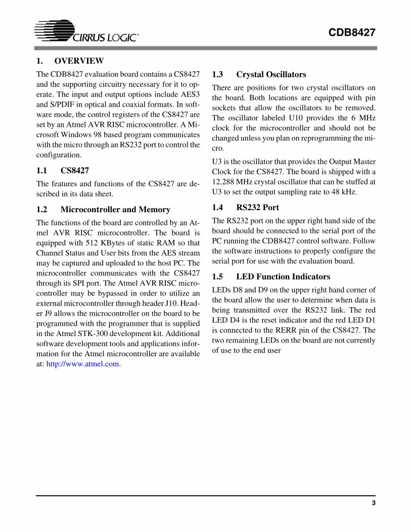
.1uF
Fig
ure
5. P
ower
Sup
plie
s an
d R
eset
Cir
cuit
11
CDB8427
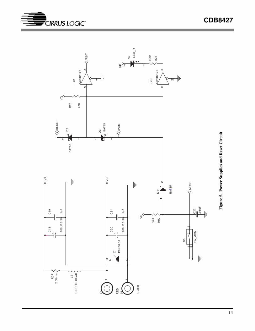
Fig
ure
6. S
ilksc
reen
12
CDB8427
Fig
ure
7. T
op P
CB
13

CDB8427
Fig
ure
8. B
otto
m P
CB
14