ccds for reductiontially low-cost version of the belgard channel vocoder algorithm. this interim...
TRANSCRIPT

CCDs FOR SPEECH BANDWIDTH REDUCTION
CNQ C. R. Hewes
ITexas Instruments Incorporated
April 1978
Semiannual Technical Report NOV2 5 2 983J
Contract No. N00173-77-C-0100
18.April 1977- 18 October 1978 1
Sponsored by
Defense Advanced Research Projects Agency
DARPA Order No. 3335
"= I .PE~~~A ?QVK,3 FOP".U:
The views and conclusions contained In this document are those of the author
and should not be Interpreted as necessarily representing the official
policies, either expressed or Implied, of the Defense Advanced ResearchProjects Agency or the U. S. Government.
US FILE COMY88 11 25 021

ATI Report No.08-78-12 i Aczsor
"NIS GRA&I .
DTIC TAB cUnannouncod 0Just it icatlo
SEMIANNUAL TECHNICAL REPORT By_ _CONTRACT NO. N00173-77-C-0100 Distribution/
18 April 1977 - 18 October 1978 Availability Codes
Sponsored by ADefense Advanced Research Projects Agency
DARPA Order No. 3335
DARPA Order Number: 3335
Name of Contractor: Texas Instruments IncorporatedCentral Research LaboratoriesPost Office Box 5936Dallas, Texas 75222
Effective Date of Contract: 18 April 1977
Contract Expiration Date: 30 June 1978
Amount of Contract: $298,507.00
Contract Number: N00173-77-C-0100
Principal Investigator and Phone No.: Dr. C. R. Hewes(2 14)238-2516
Scientific Officer and Phone No.: Dr. Dave Barbe - Code 5260Naval Research Laboratory(202) 767-2408
Short Title of Work: CCDs for Speech Bandwidth Reduction
The views and conclusions contained in this document are those of the authorand should not be interpreted as necessarily representing the officialpolicies, either expressed or implied, of the Defense Advanced ResearchProjects Agency or the U. S. Government.

TABLE OF CONTENTS
SECTION PAGE
I INTRODUCTION .. .. .....................
II ANALYZER IC .. .......... ............... 3
A. CCD Bandpass Filter .. .. .................. 3
B. CCD Topology .. ............ .......... 8
C. CCD Filter Amplifier .. .......... ........ 15
D. Full-Wave Rectifier. .. ......... ......... 18
E. Low-Pass Filter .. .. ................... 25
F. Logarithmic AID Converter. .. ......... ...... 25
G. MOS/TTL Output Buffers .. .......... ....... 29
III SYNTHESIZER. .. ........................ 31
IV STATUS AND PLANS .. .. ..................... 34
LIST OF TABLES
TABLE PAGE
I Belgard Filter Banks. .. .......... .......... 5
2 DCI Amplifier Characteristics .. ......... ....... 21
* LIST OF ILLUSTRATIONS
FIGURE PACE
I Block Diagram of a Belgard Channel Vocoder .. .. ........ 2
2 Analysis IC .. ........ ................. 4
3 Belgard Analyzer Filter Bank. .. ....... ......... 6
4 Analyzer Filter #6. .. ... ........ .......... 7
5 Analyzer Channel #6 Showing the Effects of TapweightRoundoff .. .. ...... ........ ............ 9
6 Weighting Coefficients for Analyzer Filter #6. .. ....... 10
7 Analyzer Filter #17 .. .. ......... .......... 11
8 Analyzer Filter #17 with Tapweight Roundoff .. ......... 12
9 Tapweights of Filter #17. .. .. ........ ........ 13
10 Schematic of CCD Charge Transfer Process and Clock Timing 14

LIST OF ILLUSTRATIONS(continued)
FIGURE PAGE
11 CCD Output Circuit ...... ..................... .... 16
12 Amplifier/Rectifier ...... ................... .... 17
13 Amplifier Open Loop Frequency Response .............. ... 19
14 Amplifier Closed Loop Frequency Response ............. ... 20
15 Full-Wave Rectifier Circuit and Timing Diagram .......... 23
16 Rectifier Output Waveform from Breadboard Simulation .... 24
17 Low-Pass Filter ....... ...................... ..... 26
18 Five-Bit Logarithmic A/D Converter ................ .... 28
19 MOS to TTL Output Buffers ..... ................. ... 30
20 Synthesis IC ......... ....................... .... 32
21 Two-Pole Bandpass Filter .................. 33
22 Belgard Chip Development Schedule ... ............. ... 35
ii

SECTION I
INTRODUCTION
This report concerns the progress to date in the development of analog
CCD devices to be used in the implementation of a highly integrated, poten-
tially low-cost version of the Belgard channel vocoder algorithm. This
interim report will describe both the voice analyzer and synthesizer IC
topologies, but will concentrate on the design details of only the analyzer
IC which is nearing completion of the design phase.
A simplified block diagram of the Belgard vocoder is shown in Figure 1.
In the first demonstration the two portions of the system enclosed by dashed
lines will be custom CCD/MOS LSI circuits, one for speech analysis and one
for speech synthesis, that are the subject of the current contract. The pre-
sampling and preemphasis filters are relatively simple analog filters that
ultimately can be included in the analyzer IC. The pitch extraction, framing,
and encoding will be implemented digitally using microcomputer.
At the receiving end a microcomputer will decode the digital information
and send twenty eight-bit digital words to the synthesizer IC per frame. One
of the eight-bit words contains the voiced/unvoiced decisions and the pitch
period. The excitation word is recognized by the presence of nonzero bits in
the three MSB lines and controls the excitation generator which produces pitch
pulses or random noise. The other 19 words contain the channel gains in log
PCM form. These words are D/A converted, sampled and held, and interpolated
by low pass filters to provide a gain control signal for each of the 19
channels. A summing amplifier provides a sampled-and-held audio output signal.
In Section II of this report we will describe the various circuit
functions of the analyzer IC. In Section III the synthesizer IC is outlined.
Section IV will detail our schedule and plans for the remainder of the program.

w C
cc- ot~.. E c
I- r-4In I 0
c, 410a IV I )U - Ia,~ c*
2--C
I A
cc
X 0
kAu G c
9Lo 44 &A.LE 0-
a. ia .

SECTION II
ANALYZER IC
In this section we discuss some specific details of the various components
of the Belgard analyzer IC that is shown in Figure 2. In II.A we describe
the filter characteristics to be used in the bandpass filter bank. In II.B
the CCD filters are discussed, and the other circuits are described in II.C,
II.D, II.E. II.F, and II.G.
A. CCD Bandpass Filters
Early analysis indicated that CCD transversal filters would provide a
silicon area efficient approach to fabricating the Belgard filter band.
Table I shows both the analyzer and synthesizer filter center frequencies and
bandwidth, and the Belgard filter characteristics are plotted in Figure 3.
The original Belgard system used recursive Butterworth filters (three complex
pole pairs) that we cannot exactly match with CCD transversal filters. As
described in more detail below, we will match the Butterworth characteristics
from the center of each band down to about -20 dB. Outside this region the
CCD filters will fall off much more rapidly than Butterworth characteristics,
but our stopband attenuation will be limited to about -50 dB. Discussions
with Lincoln Laboratory indicate that these characteristics will be acceptable.
The sharper filtering may perhaps be desirable and Lincoln simulations of
50 dB stopband levels prove that no performance degradation can be detected
with this stopband level.
The CCD FIR filter weighting coefficients are designed using the Parks,
McClellan, Rabiner design program with appropriate subroutine modifications
to model the Butterworth response characteristics.
Typical of the low frequency channels are the frequency characteristics
of channel #6 that are plotted in Figure 4. Both the Butterworth (smooth
curve) and the 100-stage CCD FIR characteristics are shown. The FIR response
3

LL.
9>
'II
U-
B,'.-
'B,
... *__

TABLE I
BELGARD FILTER BANKS
Center Analyzer SynthesizerChannel Frequency Bandwidth BandwidthNumber (Hertz) (Hertz) (Hertz)
I 240 120 40
2 360 120 40
3 480 120 40
4 600 120 40
5 720 120 40
6 840 120 40
7 1000 150 40
8 1150 150 40
9 1300 150 40
10 1450 150 40
11 1600 150 40
12 1800 200 60
13 2000 200 60
14 2200 200 60
15 2400 200 60
16 2700 300 60
17 3000 300 60
18 3700 300 60
19 3760 500 1 [60f= 36000
19a 3750 2(500f = 3750
I Voiced
2 Unvoiced
5


matches the Butterworth within 0.4 dB in the band center, and in the stopband
the ripple is weighted by the reciprocal of the Butterworth response in the
design program to yield a sidelobe response somewhat below the Butterworth
throughout most of the audio frequency band. The effects of weighting
coefficient roundoff (which is required by the photomask fabrication equip-
ment) can be seen by comparing Figures 4 and 5. The roundoff to the nearest
of the 500 available increments results in nonuniform sidelobe structures with
peaks in the -60 dB range for this filter as seen in Figure 5. The impulse
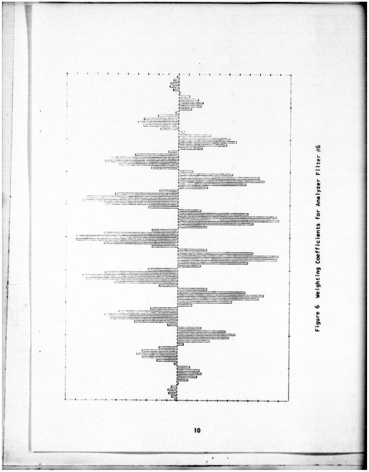
response of filter #6 can be seen in Figure 6.
The frequency response of the high frequency channels (#17) is shown in
Figures 7 and 8. As in channel #6 the roundoff limits sidelobe response,
this time to about -50 dB. The bandwidth of this filter is wider than #6,
resulting in less processing gain and greater sensitivity to roundoff error.
The impulse response plot in Figure 9 reveals a larger proportion of very
small weights, which is consistent with the greater roundoff sensitivity.
These two filters represent extremes in the design bndwidth with all
the others lying in between. We have plotted most of the other cases Pnd will
plot the remaining ones to confirm that the other cases do not produce any
unexpected problems in roundoff sensitivity and gain.
B. CCD Topology
The CCD structure for the split electrode filters will be a four elec-
trode per cell, double polysilicon device. To simplify the output sense
circuitry we will use a clocking scheme which maintains two of the four
electrodes per cell at dc potentials and that pulses the other two electrodes.
The charge transfer process is illustrated in Figure 10. Here the surface
potential is drawn (positive downward) to illustrate the potential wells for
signal electron charge packets at various times in the clock cycle. At times
tI the charges are shared under the bI and 02 electrodes and the 01 and b2
8


CNC
C, Li
In-
C 04
14,

clocks are ON (15 V). At time t 2 the 01 clock is in the OFF (0 V) state and
the charge packets have moved forward to the wells under the ON 02 electrodes.
At time t the d2 clock is OFF and the charge packets have been pushed over
the barrier created by the 2 V dc bias on the third electrode of each CCD
cell and are stored under the sense electrodes. The sense electrodes are
maintained at a constant dc potential (2.5 V) by the output circuit described
below.
The output sense circuit is a charge integrating amplifier as illustrated
in Figure 11. The difference in charge sensed by the two parts of each split
electrode is proportional to the signal charge and to the difference in the
area of the two pieces of the electrode. Thus the weighting coefficient is
obtained by controlling the positions of the split in the electrode. The
products of the weighted charge packets are summed by simply tying the elec-
trodes to two summing bus lines which form the two inputs to the integrator.
The output signal voltage is therefore
N V. (n -K)Vout (n) 1 h Kk=l 'in
in which C. is the input capacitance of the CCD, h is the filter weighting
coefficient, Cf is the gain determining feedback capacitor of the integrator,
and n is the time index.
C. CCD Filter Amplifier
The CCD bandpass filters use the split electrode technique to implement
the tapweights. This technique requires the use of an amplifier to sense
the charge on the split clock lines differentially and provide a voltage
output. This amplifier is called a differential current integrator (DCI). A
schematic of the DCl used is shown in Figure 12. The amplifier functions as
an integrator, integrating the CCD output signal onto the feedback capacitors,
CFB.
15

C~ L-
0
00clU
ar 0:3
C'44
le -C
-C cm)
Ln
VU
0.
-C )0C-
U
L
LL 0
16 L

Ir
TLIV J--4)
17U

The amplifier has two stages of differential gain with source followers
between the first and second stages. The outputs of the second differential
stage are also buffered by source followers. The dc operating point and
common mode rejection are obtained by two overlapping feedback loops connected
to the current source of each differential pair.
From the outputs of the second stage to the outputs of the first stage
are two compensating capacitors that make the second stage look like an
integrator. These compensating capacitors create a dominant pole in the
amplifier's frequency response. An additional compensating capacitor is placed
between the second differential stage outputs to create a pole at high fre-
quencies.
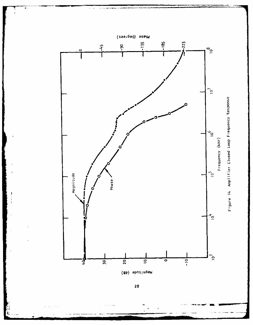
The DCl's open loop and loop transmission frequency responses are shown
in Figure 13. From the loop transmission curve the phase margin and gain
margin can be measured. The closed loop frequency response of the DCI for a
gain of 100 is shown in Figure 14. The -3 dB frequency is 125 kHz.
Because the processing gain of each filter may be different due to diff-
erent filter tapweights, the gains of the DCls must be programmed. This can
be accomplished by varying the size of the feedback capacitors. This will be
done by calculating the gain required for each filter and computer generating
the feedback capacitor.
A summary of the DCI amplifier characteristics is shown in Table 2.
D. Full-Wave Rectifier
The rectification technique is based on the capacitive source following.
A source follower with capacitive load only will act as a half-wave rectifier
if the capacitor at the source node of the transistor is precharged. When the
voltage at the source reaches (VG - VT), any signal with a level higher than
18
I!.

U% 0
U' 0 04. - -
I I I I
a
0 00
/ /0 .-
0L-
-C
0/0-
/01 0/ C(gp ap i
o I I 9
(SaaJ5aa) aseqd
LA LA LALA e0
C) 1 0
7-7
* 0 0
0~ ofl-m
00
-~ 0
* 0 .01-
UL 4)C I
_0) 0
m <~
cn -C
404
0)
C44
C 20
o 0 0No 0 -

II
TABLE 2
DCI AMPLIFIER CHARACTERISTICS
Open loop gain 41c0
Open loop bandwidth 4 kHz
Closed loop gain 50 -. 100
Closed loop bandwidth 316 kHz - 125 kHz
Phase margin 900
Gain margin 20 dB
Rise time (0 to 90% of 5 V output) 9 IS
Settling time (1%) 13 Ps
Voltage swing 5 V
Power 6.5 mW
Area 0.23 x 1.27 mm2 (9 x 50 mil )
21
7!
VG will appear at the source while any signal with a level lower than VG will
cut off the transistor. Two capacitive source followers, together with signal
inversion at one input, constitute a full-wave rectifier.
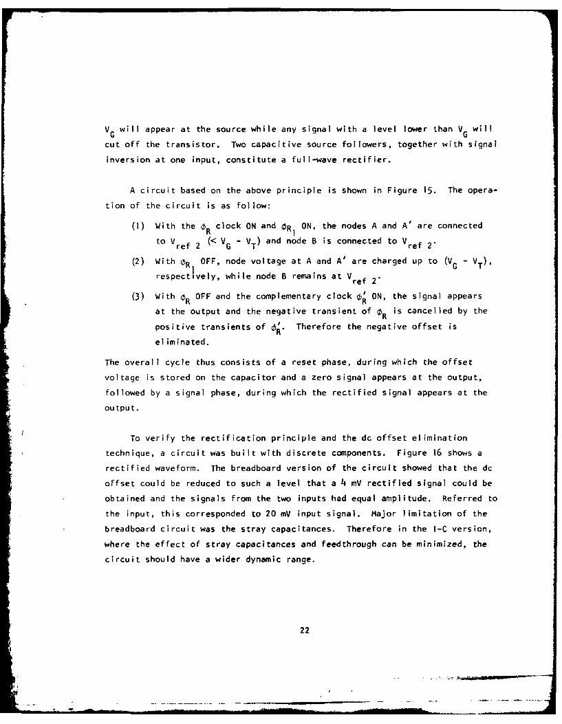
A circuit based on the above principle is shown in Figure 15. The opera-
tion of the circuit is as follow:
(1) With the 0R clock ON and R I ON, the nodes A and A' are connected
to Vref 2 (: VG " VT) and node B is connected to Vref 2"
(2) With OR OFF, node voltage at A and A' are charged up to (VG - VT),
respectively, while node B remains at Vref 2"
(3) With 0R OFF and the complementary clock 0' ON, the signal appears
at the output and the negative transient of 0 R is cancelled by the
positive transients of 0. Therefore the negative offset is
eliminated.
The overall cycle thus consists of a reset phase, during which the offset
voltage is stored on the capacitor and a zero signal appears at the output,
followed by a signal phase, during which the rectified signal appears at the
output.
To verify the rectification principle and the dc offset elimination
technique, a circuit was built with discrete components. Figure 16 shows a
rectified waveform. The breadboard version of the circuit showed that the dc
offset could be reduced to such a level that a 4 mV rectified signal could be
obtained and the signals from the two inputs had equal amplitude. Referred to
the input, this corresponded to 20 mV input signal. Major limitation of the
breadboard circuit was the stray capacitances. Therefore in the I-C version,
where the effect of stray capacitances and feedthrough can be minimized, the
circuit should have a wider dynamic range.
22

V
5 -" v R 2
Vo DO" 0-4 V ref I
RII
ref 2
T 5 pFR
v in(-
Signal
R
Figure 15 Full-Wave Rectifier Circuit and Timing Diagram
23

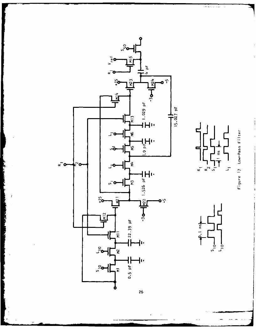
E. Low-Pass Filter
The analysis chip requires a three-pole, Butterworth low-pass filter -jith
f = 35 Hz to filter the output of the rectifier. A switched capacitor type,c
sampled-data, low-pass filter was designed to meet this requirement.
The circuit is shown in Figure 17. It consists of an R-C sectirn in
cascade with a Sallen-Key type, low-pass filter. The R-C section pro.;Ju a
real pole while the Sallen and Key section provides the remaining two complex
poles. Different clock rates are used in the two sections in order to
minimize the on-chip capacitor area. The R-C section is to be operated at a
clock rate of 10 kHz while the clock rate for the Sallen and Key section is
1 kHz.
Because of the dc offset problem inherent with MOSFETs, it is necessary
to use ac couple, dc restore techniques to eliminate the effect of VT variation.
With R ON, R OFF, the source followers are isolated from the rest of the12
circuit. The dc offset is stored on C . With R2 ON and R I OFF, every one-
tenth of input data will appear at the output.
The circuit has been designed and simulated on IBM 370. Its tnral area2
is about 30 x 9 mi] . The values of capacitors shown in Figure 17 represent a
cGmpromise between area and sensitivity.
F. Logarithmic A/D Converter
Signal dynamic range compression and analog-to-digital conversion are
accomplished in the logarithmic A/D converter. The 19 low-pass filter outputs
are multiplexed into the A/D converter at a I kHz rate. The converter output
is a five-bit word with a lI dB step size. Therefore the total dynamic range
of input signal covered is 48 dB.
25
UI-
,H -I
2 0
- 3
01~
-T4-262

A block diagram of the converter is shown in Figure 18. Logarithmic
response is obtained with an array of eight polysilicon capacitors (C0 - C7)
weighted such that the sum
7C sum Z C for i =0-7
n--i
is incremented in 6 dB steps and with a polysilicon resistive divider (R0 - R )
which makes available four reference voltages (V0 - V3 ) and a reset voltage
Vrese t spaced Il dB apart to the capacitor array. A successive approximation
technique is used to determine the digital word. A 10-stage shift register
(SRIO) clocked by 10 kHz pulses RIO and SIO continuously circulates a single
"l" bit to provide sequencing for the A/D converter. When SRlO 0 is high the
converter goes through a reset cycle. At this time the latches containing
the digital output (Q, - Q5) are reset to "0" and the bottom plates of the
capacitors C0 - C7 are clamped to Vrese t while the signal amplifier and the
high gain comparator A2 are reset. A signal from one of the 19 low-pass
filter outputs is then applied to C Sig by the Al amplifier. The signal is
inverted by Al and appears on node n attenuated by j by the capacitor array.c
The comparator saturates in the high state if the signal is greater than
4q mv.
To determine the first three bits (QI, Q2, Q ) of the digital output,
LATCH I through LATCH 3 are sequentially set to "1" by the shift register.
When LATCH 1 is set, the CAPACITOR DECODE circuit causes the bottom plates of
capacitors C3 - C7 to be switched from V reset to Vswitch (Vswitch - V at
this time). This causes the voltage on node n to increase by an amountc
proportional to C3 + C4 + C5 + C6 + C7 and to V0 (251 dB). If this voltage
increase is greater than the decrease that was caused by the signal, then the
comparator A2 will change state and at the end of this cycle the QI output of
LATCH I will be reset to "0." If the voltage increase is not enough to cause
27

-1r
Li
7-'J
0c -- rUC
00
I I.
28

the comparator to change state, then the Q, output of LATCH I will remain set
to "1." Bits 02 and Q3 are determined in the same fashion, after which the
capacitors that bring the voltage on node nc to within 6 dB below the compara-
tor switching threshold remain clamped to V switch The other capacitors are
clamped to Vreset . Next LATCH 4 is set causing the voltage Vswitch to
increase by 3 dB from V to V This causes the voltage on node nc to
increase by 3 dB. If the comparator changes state, then the 04 output of
LATCH 4 is reset to "Oi; otherwise it remains 1116. Q is determined in the
same way. The digital word is now completely determined and the shift
register (SRI0 8) causes the MOS to TTL converters to sample the word. SRIO0
provides a data-ready signal to the microprocessor which then has 800 as to
read the word.
G. MOS/TTL Output Buffers
The analyzer A/D converter has six output signals, five data lines, and
a data-ready signal. Each of these is buffered by an identical amplifier to
provide TTL level outputs with a fanout of two standard loads. A computer
model of the circuit indicates that each amplifier will dissipate 0.67 mW and
that the rise and fall times under maximum load are 80 to 90 ns. Each
amplifier consumes 0.65 x 10⁻⁵ cm2 (36 mil 2 ) of surface area.
The schematic diagram of one of these drivers is shown in Figure 19.
The circuit consists of two depletion load inverters, a flip-flop, and a
push-pull output stage. Transistor pairs MI, M3 and M42, M4 form the two
inverters. The inverted input signal appears on node A and the true signal
reappears on node B where the levels now are 0 V and V (15 V). These
signals are applied to the load transistors (M5 and M6) of a flip-flop, and
the outputs of the flip-flop drive the push-pull output stage (M9 and 14O).
Because the flip-flop and the push-pull stages are composed of enhancement
mode devices, there is no quiescent current required, resulting in the low
on-chip power dissipation.
29

Input33
M I CC
TTfopail Otu
Fiur 19MSt Otu ufr
30M0

SECTION III
SYNTHESIZER IC
The synthesizer IC block diagram is shown in Figure 20. The details of
this IC will be provided in a laL'er report, but a brief general description
will be provided below.
The synthesizer IC will have a D/A converter whose output will be
demultiplexed into 19 sample-and-hold circuits, i.e., one for each channel of
the synthesizer filter bank. Each sample-and-hold operates at the frame rate
and the outputs of the sample-and-hold circuits are interpolated up to a
10 kHz sample rate by a two-stage low-pass filter similar to those in the
analyzer IC. The outputs of the low-pass filters modulate the excitation of
the corresponding channel bandpass filters. The bandpass filters will be a
recursive switch capacitor, two-pole filter of the type shown in Figure 21.
The excitation will be generated on chip from the digital input data. A PLA
structure will provide the pitch period for voiced sounds and a pseudorandom
sequence will provide the noise excitation. Summing of the channels will also
be provided on chip as well as clocks for the filter functions.
31
.4

.I.
L N
D 0. t 114, 41
10 M
Q. E
___i__
L-
to r-ro,
41,
4,. . -
O,,,E L
UU
I-COS
* >
32

V.
III
Sn ° "vA /"-
vou t
Figure 21 Two Pole Bandpass Filter
33

1a
SECT ION IV
STATUS AND PLANS
Our current development schedule is shown in Figure 22. As indicate.d,
the analyzer chip circuit design is completed and the layout is in the fina.
phase. There were recent delays that slipped our schedule about t.,, weh-;
on the analyzer chip that were due to technical reasons.
Analysis of the rectifier indicated there were potential offset.
problems that we have now solved.
* We made the decision to convert the design to a new simplified -CD
fabrication process that we demonstrated in January and Fehrua-,'.
This process offers higher dynamic ranges, better amplifier perfor-
mance, higher density, and higher yield and compatibility with
production lines.
Currently we expect to complete chip fabrication of the analyzer ICs in
early June and, after evaluation, ship some of them to Lincoln Laboratory for
testing by the end of July. We will continue extensive testing and evaluation
throughout the remainder of the program to aid in redesign activities later.
The synthesizer IC will use many of the same circuit elements as the
analyzer IC, e.g., op amps, capacitive array for the D/A converter. The
filter bank is being designed now and we expect to start bar layout by the
first of May. The fabricated ICs should be completed by mid-September and we
expect to be able to deliver the synthesizer iCs to Lincoln Labs for evaluation.
34
I L _ I.-"- . --

1978
Analyzer IC M A M A S 0
Complete DesignLayoutPhotomasksFabrication of ICsTestingDelivery of Analyzer Chips to
MIT Lincoln Laboratory
Synthesizer ICDesignLayoutPhotomaskFabrication of ICsTestingDelivery
Figure 22 Belgard Chip Development Schedule
35