ccds and cmos imagers - university of arizonaircamera.as.arizona.edu/astr_518/astr518_lesser.pdf ·...
TRANSCRIPT

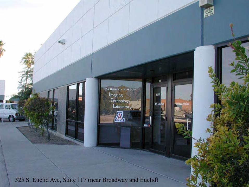
325 S. Euclid Ave, Suite 117 (near Broadway and Euclid)

Imaging Detectors
4kx4k buttable CCD
CMOS imager
Magacam focal plane (Magellan)
90Prime
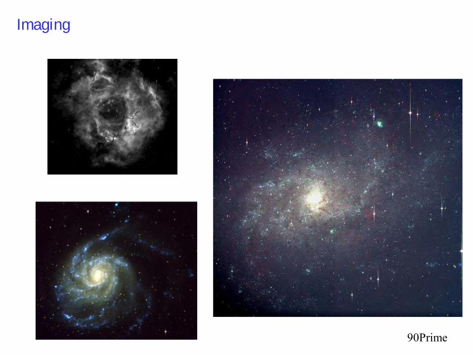
Imaging
90Prime
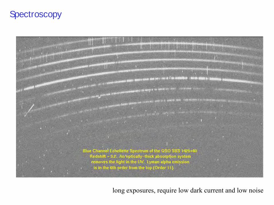
Spectroscopy
long exposures, require low dark current and low noise

Recent Scientific Detector Progress
• Bigger and bigger devices – 10kx10k CCDs (1 die per 150 mm diameter silicon wafer) – 10kx10k CMOS imagers (commercial only so far…)
• Orthogonal Transfer Arrays (OTA) – WIYN ODI, PanStarrs
• Extended spectral response – UV (193 nm and below), X-ray, direct electron bombardment – 800 – 1000 nm QE > 80%, reduced fringing
• Extremely tight mechanical specifications – 5 um peak-valley flatness
• Large mosaics with buttable detectors – ~100 devices now, 200+ in next few years – mosaics of 10kx10k detectors
• CMOS imagers – on-chip logic, lower voltages and power,
radiation hard, recent low noise results, lower cost?

CCD Architectures
Full frame
– entire area of CCD used to collect image – best use of area, most common in astronomy – requires a shutter during readout
Frame transfer
– frame store half of CCD covered with opaque mask – image store half is unmasked and collects photons during integration – rapid shift (1 – 100 millisecond) from image store to frame store after exposure (image and store parallel clocks must be separate) – frame store read slowly while image store integrates next exposure – reduces “dead time” – no shutter required – only half of silicon area collects light
frame transfer
split frame transfer
full frame

CCD Architectures
Interline transfer
– opaque transfer bus along each column – rapid shift from each pixel (or photodiode) to bus after exposure – bus pixels readout during next exposure – reduces dead time – no shutter required – significant opaque area – fill factor < 1 even in image area – common in cell phones and video cameras
Possible to increase fill factor by using microlenses, typically made by applying photoresist to surface, etching, and thermal processing to produce lens shape.
photosite
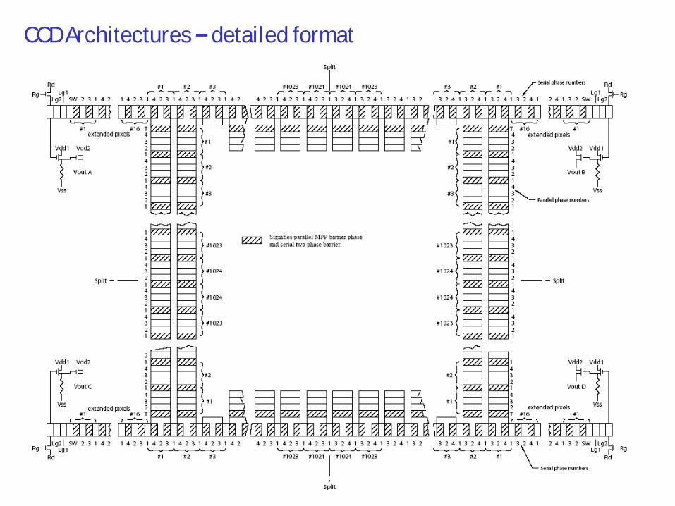
CCD Architectures – detailed format

CCD Clocking
4-phase 2-phase
implant
modifies
channel
potential

CCD Pixel Binning
• Timing pattern may be changed so charge from multiple pixels are added together
• Decreases spatial resolution of detector as creates bigger effective pixels • Allows higher charge capacity and so larger dynamic range • Increases read out speed since each pixel is not sampled at output • Binning can be performed in columns or rows, with different binning factors • Serial register pixels are usually made 2x the size of image pixels to allow
2x charge capacity • Many CCDs have an Output Summing Well which is the last pixel of a serial
register, independently clocked, and 2x the size of a serial pixel, to aid in binning • Also called noiseless co-addition since summing comes before readout, when
read noise is generated
• For a shot-noise limited, uniform exposure,
1/ 2[ ( )]H VSNR P P S e where S(e-) is the average unbinned signal in electrons per pixel and Px are binning factors
CCD Charge Transfer
( ) exp( )!
n
iN n
S N CTIS N CTI
n
• The charge found n pixels after target pixel (Si) following N pixel shifts is
• Charge in a pixel after N pixel shifts is ( )N
N iS S CTE
Example: An Fe-55 X-ray event (1620 e-) in the far corner of a 4kx4k device will contain only 1493 e- at the output amplifier if CTE = 0.999990 (92%)
Si is initial charge in pixel before shifting
CTE = Charge Transfer Efficiency = 1 - CTI
Fe-55 X-ray illumination is a common method of measuring CTE, gain, charge diffusion, and noise. Each event creates a fixed number of photoelectrons in a small (~1 um) cloud. Fe55 x-rays (5.9 keV) do not pass through a glass dewar window.

CCD Charge Transfer
Fe55 image analysis – histogram and CTE plots

CCD CTE Problems
• line trap – typically due to a short between phases in the image area
• parallel clock voltage at gates near short are reduced
• increased applied gate voltage increase normally reduces trap size by increasing effective Vgate near trap
• fat zero or preflash may fill traps – very low level exposure or direct input before integration exposure (adds noise)
global CTE problem – silicon issue?
line trap

Silicon Dark Current
/ 215 1.5( ) 2.5 10 gE kT
pix FMD e x A D T e DFM is nA/cm2 @ 300K
Apix pixel area (cm2)
parameter is pA/cm2 @ 293K
scientific CCD dark signal is typically <10 e/pixel/hour @ -100 C
Back Illuminated CCDs
• Optical absorption and multiple reflections from frontside structures (polysilicon gates and oxides) reduce efficiency.
• No blue/UV transmission through polysilicon. • Solution is the thin CCD and illuminate detector from backside. • Must remove highly doped p+ material which CCD is fabricated with to leave only
epitaxial material. Typically 10-50 m thick (100 m for LSST). • Interference fringing is worse than for thick devices. • If a field-free region remains between the back surface and edge of depletion
region, then charge spreading occurs and resolution is degraded. Worse in the blue as photoelectrons are generated near the back surface.
• Backside surface is a disrupted silicon crystal which has dangling chemical bonds, creating a positively charged interface. This traps electrons at the backside and so a freshly thinned CCD has very poor QE.
• Adding a negative charge to the back surface is called backside charging and lead to very high QE devices when coupled with AR coatings.
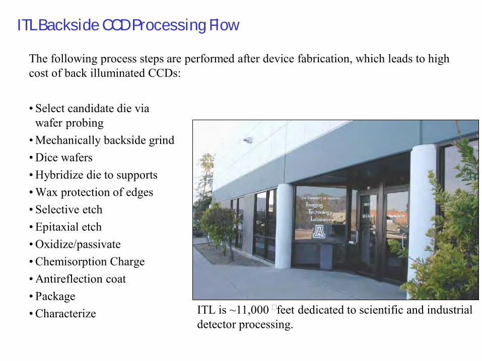
ITL Backside CCD Processing Flow
• Select candidate die via wafer probing
• Mechanically backside grind • Dice wafers • Hybridize die to supports • Wax protection of edges • Selective etch • Epitaxial etch • Oxidize/passivate • Chemisorption Charge • Antireflection coat • Package • Characterize
The following process steps are performed after device fabrication, which leads to high cost of back illuminated CCDs:
ITL is ~11,000 feet dedicated to scientific and industrial detector processing.

UA Foundry Wafer
• STA design with fabrication though DALSA (now Teledyne DALSA)
• ITL post-fabrication processing
• 2 4kx4k CCDs
• 4 2688x512 CCDs
• 4 1200x800 CCDs
• 512x1024 FT guiders
• 128x128 AO devices
• FBI test devices
There are very few fabs in the world making scientific CCDs.

• world’s largest integrated circuit • 1 die per 150 mm wafer • 9 µm pixels • 16 high speed outputs • probing challenge • detector for LBT PEPSI instrument
STA1600A 10kx10k CCD
150 mm silicon wafer, one die per wafer
PEPSI dewar with CCD

STA0500A Back Illuminated CCD
• Typical hybridized large format CCD • CCD hybridized to thick silicon substrate for flatness • Indium and gold bumps • Epoxy underfill • Die attached & wire bonded to Kovar, Invar, or ceramic package • Detector cost ~ $50,000 back illuminated (< $25k front illuminated)
STA0500 4kx4k 15 m pixels
s ilic o n s u b s tra te
m e ta l p a c k a g e
W ire b o n d s
p in s
C C D
bumps

Wafer Probing for Scientific Detectors
• DC defects get worse when backside thinned • Test shorts to 20 M • AC image (-60 C)
STA2200 Orthogonal Transfer Array CCD @ -60 C

Wafer Dicing
Dicing saw Dicing chuck
UV tape releaser Wafer taper

Detector Hybridization
• Flip chip bonders are used to align and bond detectors and substrates • Infrared or split field aligners • Similar to technology used to hybridize IR arrays to readouts
Stud bumper places gold bumps on each detector I/O pad

Detector Protection for Etching
space applications
Partial thinning (Antarctic 10k)
Wax dispensing
thick region
thin region

Acid Etching
• 1:3:8 HF:HNO3:CH3COOH acid solution used to etch • Etch selectivity critical to achieve uniform thickness • Typical doping levels p+ = 1018 cm-3; p = 1015 cm-3
4 hybridized die
Epitaxial etch
acid benches

Backside Coatings
ITL’s Chemisorption Process: • Oxidize backside of thinned CCD to reduce interface trap density • Apply thin metal film (10A silver) to promote negative backside charge • Apply antireflection coating optimized for spectral region of interest
Oxidation chamber
AR coating chamber
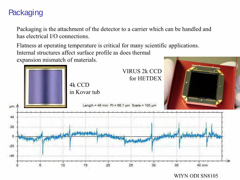
Packaging
Packaging is the attachment of the detector to a carrier which can be handled and has electrical I/O connections. Flatness at operating temperature is critical for many scientific applications. Internal structures affect surface profile as does thermal expansion mismatch of materials.
WIYN ODI SN8105
VIRUS 2k CCD for HETDEX
4k CCD in Kovar tub

Packaging - Buttable Imager of WIYN ODI and LSST
top bottom
Aluminum Nitride ceramic
CE5 frame: Silicon Aluminum alloy for good thermal conductivity and thermal expansion match to silicon/ceramic
LSST
One Degree Imager

Wire Bonding
Wire bonder
Pull testing wire bonds for QA

Low Temperature Detector Metrology
ITL “Cryoscanner” • Nanovea profilometer pens on large open frame stage
with vibration isolation frame holding dewar • Metrology performed from +25 C to -150 C
LN2 cooled dewar

LSST Prototype Sensor Metrology
0 2.5 5 7.5 10 12.5 15 17.5 20 22.5 25 27.5 30 32.5 35 37.5 40 mm
µm
-2
-1
0
1
2
0 10 20 30 mm
mm
0
5
10
15
20
25
30
35
µm
-3
-2.5
-2
-1.5
-1
-0.5
0
0.5
1
1.5
2
2.5
3
data from CryoScanner @ -137 C ~4 m peak-valley LN2 ‘dunker’
room temp profilometer

Curved Detectors
University of Arizona Imaging Technology
Laboratory
Early curved devices @ ITL in mid-1990’s but renewed interest from ESO for ELT Reduce optical complexity or increase optical efficiency Its fun when detectors explode!
500 mm radius of curvature
25 mm radius (1D)
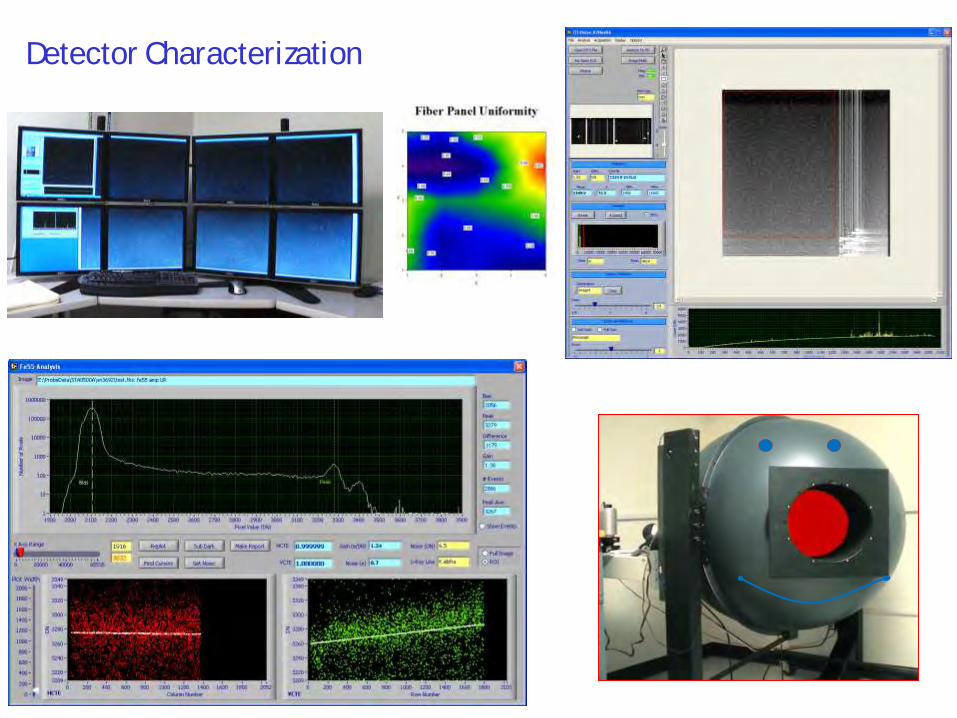
Detector Characterization

Quantum Efficiency
The absorptive quantum efficiency QEabs is the fraction of incident photons which is absorbed in the detector,
( )( )0 0
0
(1 ) (1 )(1 )a x
a x
abs
S S eQE r r e
S
where x is the thickness of the detector and r is the reflectivity from the incident surface, is the absorption coefficient, S0 is number of incident photons.
Increase QE by…
1. reducing reflectivity with antireflection (AR) coatings
2. increasing absorption coefficient (material selection)
3. increasing thickness of absorbing material

Backside CCD QE
0%10%20%30%40%50%60%70%80%90%
100%
0.3 0.4 0.5 0.6 0.7 0.8 0.9 1
Wavelength (um)
Mea
sure
d Q
E
Kodak KAF260
Thomson THX7398
Loral LM
Orbit 2kx4k

Backside CCD QE - Ultraviolet
0%10%
20%30%40%50%
60%70%80%
90%100%
200 300 400 500 600 700 800 900 1000 1100
Wavelength (nm)
Mea
sure
d Q
E
200A HfO2
150A HfO2

QE vs. Temperature
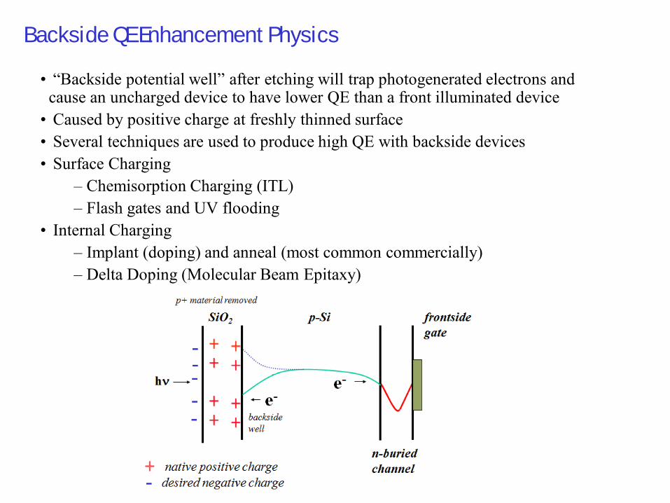
Backside QE Enhancement Physics
• “Backside potential well” after etching will trap photogenerated electrons and cause an uncharged device to have lower QE than a front illuminated device
• Caused by positive charge at freshly thinned surface • Several techniques are used to produce high QE with backside devices • Surface Charging
– Chemisorption Charging (ITL) – Flash gates and UV flooding
• Internal Charging – Implant (doping) and anneal (most common commercially) – Delta Doping (Molecular Beam Epitaxy)

QE Instability
Incomplete backside charging may cause temperature and time dependent QE variations because the back surface is not pinned with the required negative charge density to drive all photoelectrons to the detector frontside.
0%10%20%30%40%50%60%70%80%90%
100%
0.2 0.3 0.4 0.5 0.6 0.7 0.8 0.9 1 1.1Wavelength (um)
Mea
sure
d Q
E
+23 C 0 C-85 C
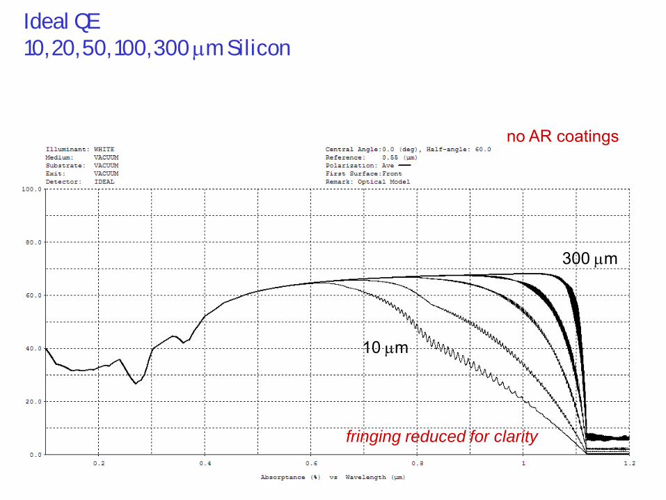
Ideal QE
10, 20, 50, 100, 300 m Silicon
no AR coatings
fringing reduced for clarity
10 m
300 m

LSST CCD - 93 m thick
LSST STA1759ASN7425
0%
10%
20%
30%
40%
50%
60%
70%
80%
90%
100%
300 400 500 600 700 800 900 1000 1100
Wavelength (nm)
Mea
sure
d Q
E
+25CComparision to 17 micron thick device with same AR coating
University of Arizona Imaging Technology Laboratory
M. Lesser 16Jan08
SN7425

Interference Fringing in Detectors
When the absorption length is large compared to the detector thickness, light can reflect multiple times between the front and back surfaces of a detector. This leads to constructive and destructive optical interference within the detector.
CCD image with fringing
zoomed fringing
QE plot of back illuminated CCD

Antireflection Coatings
• An AR coating is a thin film stack applied to the detector surface to decrease reflectivity; typically used on all modern imagers.
• Coating materials should have proper indices and be non-absorbing in the spectral region of interest.
• With absorbing substrates which have indices with strong wavelength dependence (like silicon), thin film modeling programs are required to calculate reflectivity.
• Designer must consider average over incoming beam (f/ ratio) and angle of incidence due to angular dependence.

uncoated Si
1 layer - 550 A HfO2
2 layer – 500 A HfO2 + 1000A MgF2
Silicon Reflectivity

Ideal QE with AR Coatings
50 m silicon uncoated + 1 layer + 2 layer

Fully Depleted Devices
• Fully depleted (300 m thick at LBL, 50 m thick commercially). • Greatly reduced interference fringing and very high near-IR QE. • Backside bias contact required for depletion (~100 V). Must be transparent. • Very high resistance (ultra pure) silicon required to support complete depletion. • Problems include sensitivity to cosmic rays, higher dark current, backside
contact, and charge spreading (resolution loss).
300 m fully depleted CCD QE

Field Free Region – Charge Spreading
The region in a back illuminated CCD between the edge of the depletion region and the back surface is the “field-free” region.
Photogenerated electrons can diffuse in all directions in this region, reducing resolution through charge spreading.
Experimentally,
1/ 22 (1 )ff ff
ff
LC x
x
Cff is the lateral diffusion diameter, xff is the field free thickness, and L is the distance from the backside surface where the photoelectron is generated
Higher resistivity material has deeper depletion region (~ 1/NA), so xff is smaller. 50 cm material typical, but 1000-10,000 cm possible.
5 m FF region => 10 m electron cloud
e- field free region
xff
L

Charge Diffusion – “Full Depletion”
-50 V backside bias no backside bias
Fe-55 X-ray events 93 m thick LSST CCD
Cooling of custom silicon
for high resistivity detectors
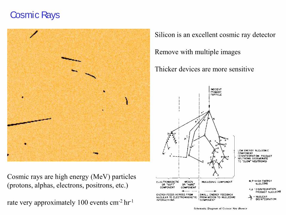
Cosmic Rays
Silicon is an excellent cosmic ray detector Remove with multiple images Thicker devices are more sensitive
Cosmic rays are high energy (MeV) particles (protons, alphas, electrons, positrons, etc.) rate very approximately 100 events cm-2 hr-1
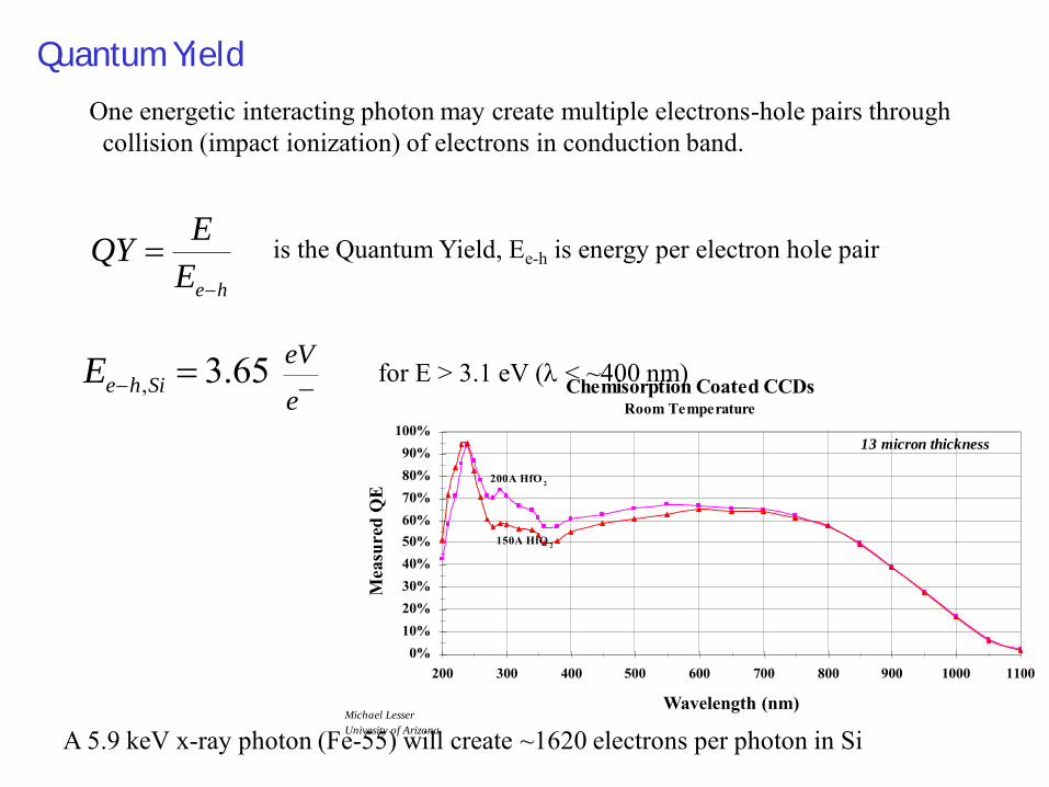
Quantum Yield
One energetic interacting photon may create multiple electrons-hole pairs through collision (impact ionization) of electrons in conduction band.
e h
EQY
E
, 3.65e h Si
eV
eE
A 5.9 keV x-ray photon (Fe-55) will create ~1620 electrons per photon in Si
for E > 3.1 eV ( < ~400 nm)
is the Quantum Yield, Ee-h is energy per electron hole pair
Chemisorption Coated CCDsRoom Temperature
0%10%20%30%40%50%60%70%80%90%
100%
200 300 400 500 600 700 800 900 1000 1100
Wavelength (nm)
Mea
sure
d Q
E
200A HfO 2
150A HfO 2
13 micron thickness
Michael Lesser
Univesity of Arizona

Detectors with Internal Gain
Some non-photoemissive detectors can also have electron gain and may be used for photon counting or very low light level applications.
• Avalanche photodiodes have gain due to impact ionization when the photoelectron is accelerated in a very high electric field within the silicon.
• Internal gain CCDs (TI and E2V) utilize an extended serial register and a very high electric field within each pixel. As the CCD shifts charge through this extended register, a small avalanche gain (1.01) is achieved. After ~100 gain stages, an electron packet larger than the read noise is generated and photon counting is possible.
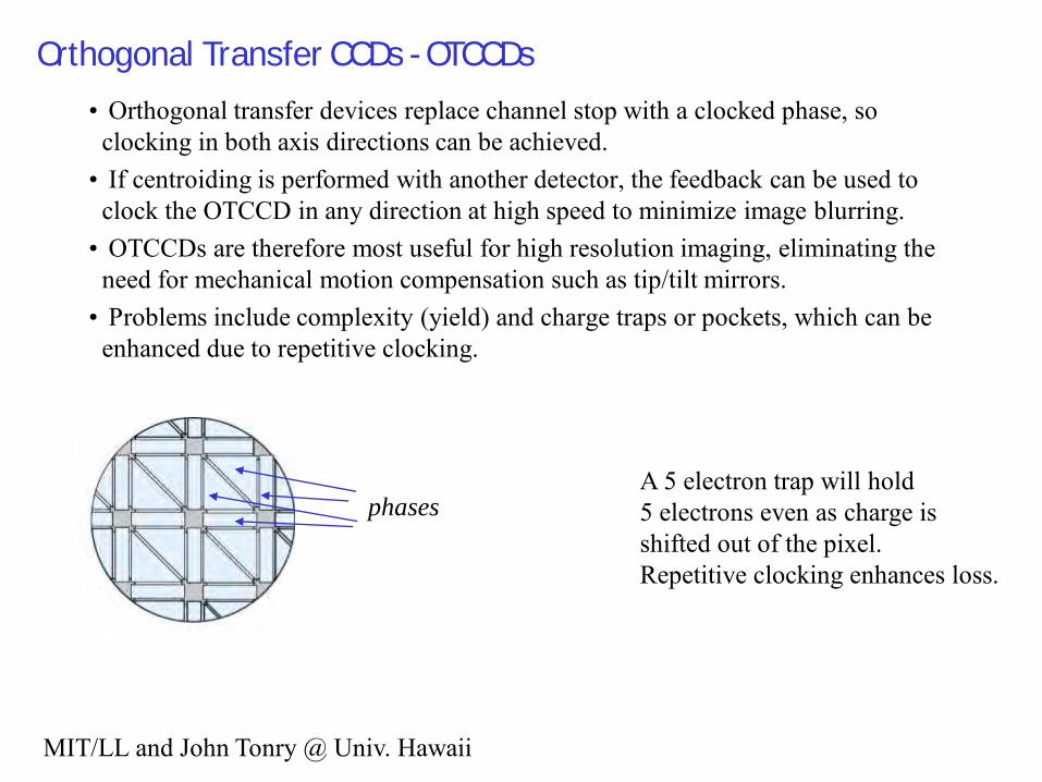
Orthogonal Transfer CCDs - OTCCDs
• Orthogonal transfer devices replace channel stop with a clocked phase, so clocking in both axis directions can be achieved.
• If centroiding is performed with another detector, the feedback can be used to clock the OTCCD in any direction at high speed to minimize image blurring.
• OTCCDs are therefore most useful for high resolution imaging, eliminating the need for mechanical motion compensation such as tip/tilt mirrors.
• Problems include complexity (yield) and charge traps or pockets, which can be enhanced due to repetitive clocking.
phases A 5 electron trap will hold 5 electrons even as charge is shifted out of the pixel. Repetitive clocking enhances loss.
MIT/LL and John Tonry @ Univ. Hawaii

The Orthogonal Transfer Array (OTA)
OTCCD pixel structure
Basic OTCCD cell OTA:
8x8 array of OTCCDs
Pan-STARRS and WIYN ODI projects will use OTAs, which monolithic arrays of OTCCDs
Advantages include low susceptibility to internal shorts and restriction of full well blooming to single OTCCD cells. Low shorts->high yield->low cost
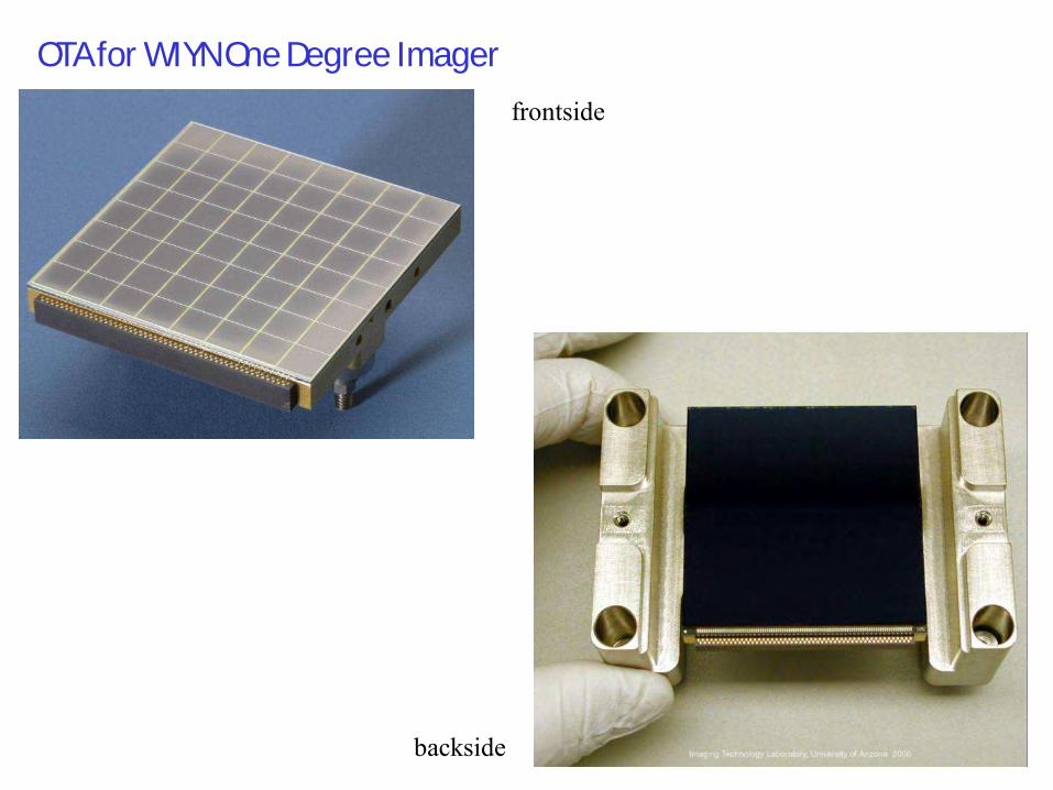
OTA for WIYN One Degree Imager
frontside
backside
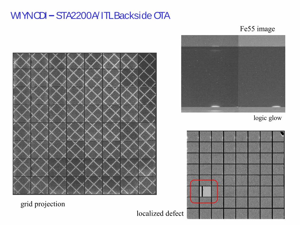
WIYN ODI – STA2200A/ITL Backside OTA
grid projection
Fe55 image
localized defect
logic glow

Focal Plane Assembly
Assembly of 14 backside devices onto focal plane
Installation of flex cables on backside of focal plane
Transport and assembly cart

Focal Plane Assembly
backside detail of PGA connector & flex cable
custom tool for flex installation
backside before flex installation

Focal Plane Assembly
Final pODI focal plane on VIEW Summit 600 CMM
~25 um peak-valley

CMOS Imagers
CMOS imagers utilize a CMOS fabrication process to create an array of photosensors, typically photodiodes. Common devices are monolithic in which readout circuitry is on the same device as the photosensors or hybrid in which the detector is hybridized or flip chip bonded to the readout.
Called active pixel sensors (APS) or passive pixel sensors (PPS), depending on pixel structure

CCD - CMOS Readout Comparison
CMOS Imager
amps in every pixel
CCD Imager
few amps per device
From Janesick, OE Magazine, February 2002

CMOS Advantages
• Very low power usage – no high voltage required for amps, no large clock voltage swings for charge transfer, little off-chip electronics, 5 or 3.3 V operation.
• Radiation tolerate – CMOS fabrication process. • ULSI – digital circuitry allows “on-chip” processing functions, such as ADC,
logarithmic gain, multiple sampling, image compression, anti-jitter, color, etc. • Random access of pixels – charge to voltage conversion at each pixel. • No CTE issues as no charge transfer – less susceptible to traps. • CMOS compatible with 90% of silicon fabrication facilities.
Single power source in and digital output is very attractive.

CMOS Disadvantages
• Fill factor is relative size of photosensor to pixel size. Smaller scale design rules for fabrication allow higher fill factor, but is always < 100%. Typically <50%.
• Noise higher than CCD due to amplifier designs which must drive busses with higher current.
• Fixed pattern noise high compared to CCDs due to pixel to pixel and column to column gain variations (thousands of amplifiers and capacitors). Typically 0.1 – 3% variations. Very complex integrated circuits.
• Circuitry generates heat which increases (local) dark current. • Shallow p-n junctions of CMOS processes limit light sensitivity.
• Commercial push is toward VERY small pixels (1 m) for consumer electronics.

4kx4k 15 um pixel CMOS Imager
Micron Technology, Inc.- 4kx4k 15 m pixel CMOS imager
UA Imaging Technology Laboratory

Back Illuminated CMOS Imagers
• Illuminate from backside to enhance QE as with CCDs • Avoid stimulating current in active pixel areas which can lead to ‘latchup’
photons
Backside processing is similar to CCDs with the same silicon properties
Backside CMOS imager
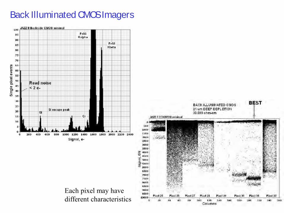
Back Illuminated CMOS Imagers
Each pixel may have different characteristics
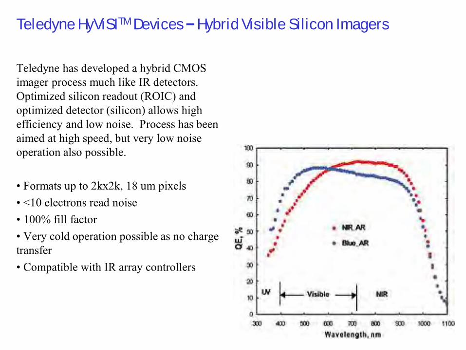
Teledyne HyViSITM Devices – Hybrid Visible Silicon Imagers
Teledyne has developed a hybrid CMOS imager process much like IR detectors. Optimized silicon readout (ROIC) and optimized detector (silicon) allows high efficiency and low noise. Process has been aimed at high speed, but very low noise operation also possible. • Formats up to 2kx2k, 18 um pixels • <10 electrons read noise • 100% fill factor • Very cold operation possible as no charge transfer • Compatible with IR array controllers

Color Sensing – CMOS and CCD
G R G R G R G R G R B G B G B G B G B G G R G R G R G R G R B G B G B G B G B G
Bayer pattern commonly used
• Color filters placed over each pixel and imaging processing is used to determine an ‘average color’ for each pixel based on local adjacent intensities. • Low sensitivity and spatial resolution compared to monochrome imagers due to filters
not used in astronomy

References
“Scientific Charge-Coupled Devices”, James Janesick, SPIE Press Monograph Vol. PM83 , 2001 “Fundamental performance differences between CMOS and CCD imagers: Part II”, Janesick, James; Andrews,
James; Tower, John; Grygon, Mark; Elliott, Tom; Cheng, John; Lesser, Michael; Pinter, Jeff, Proc. SPIE 6690, p. 3, 2007, also parts I and III
“Very Large Format Back Illuminated CCDs”, Lesser, Michael in Scientific Detectors for Astronomy, Amico, P., Beletic, J. W., and Beletic, J. eds, Kluwer Academic Publishers, 2004, p.137
“Secrets of E2V Technologies CCDs”, Jorden, P. R.; Pool, P.; Tulloch, S. M., Scientific Detectors for Astronomy, The Beginning of a New Era; eds., Amico, P.; Beletic, J. W.; Beletic, J. E., p. 115-122, 2004
http://www.itl.arizona.edu http://www.hamamatsu.com http://www.sta-inc.net http://www.sri.com/engage/products-solutions/imaging-solutions http://www.e2v.com http://www.fairchildimaging.com http://www.ll.mit.edu/mission/electronics/AIT/aithome.html