cc1350 simplelink ultralow-power dual-band wireless mcu · cc1350 simplelink™ ultra-low-power...
TRANSCRIPT
Product
Folder
Sample &Buy
Technical
Documents
Tools &
Software
Support &Community
An IMPORTANT NOTICE at the end of this data sheet addresses availability, warranty, changes, use in safety-critical applications,intellectual property matters and other important disclaimers. PRODUCTION DATA.
CC1350SWRS183 –JUNE 2016
CC1350 SimpleLink™ Ultra-Low-Power Dual-Band Wireless MCU
1 Device Overview
1
1.1 Features1
• World's First Dual-Band (Sub-1 GHz and 2.4 GHz)Wireless Microcontroller
• Microcontroller– Powerful ARM® Cortex®-M3– EEMBC CoreMark® Score: 142– EEMBC ULPBench™ Score: 158– Clock Speed Up to 48-MHz– 128KB of In-System Programmable Flash– 8KB of SRAM for Cache
(or as General-Purpose RAM)– 20KB of Ultra-Low-Leakage SRAM– 2-Pin cJTAG and JTAG Debugging– Supports Over-the-Air (OTA) Update
• Ultra-Low-Power Sensor Controller– Can Run Autonomously From the Rest of the
System– 16-Bit Architecture– 2KB of Ultra-Low-Leakage SRAM for Code and
Data• Efficient Code-Size Architecture, Placing parts of
TI-RTOS, Drivers, Bluetooth® low energyController and Bootloader in ROM
• RoHS-Compliant Package– 7-mm × 7-mm RGZ VQFN48 (30 GPIOs)
• Peripherals– All Digital Peripheral Pins Can Be Routed to
Any GPIO– Four General-Purpose Timer Modules
(Eight 16-Bit or Four 32-Bit Timers, PWM Each)– 12-Bit ADC, 200 ksamples/s, 8-Channel Analog
MUX– Continuous Time Comparator– Ultra-Low-Power Clocked Comparator– Programmable Current Source– UART– 2× SSI (SPI, MICROWIRE, TI)– I2C, I2S– Real-Time Clock (RTC)– AES-128 Security Module– True Random Number Generator (TRNG)– Support for Eight Capacitive Sensing Buttons– Integrated Temperature Sensor
• External System– On-Chip Internal DC-DC Converter– Seamless Integration With the SimpleLink™
CC1190 and CC2592 Range Extenders
• Low Power– Wide Supply Voltage Range: 1.8 to 3.8 V– RX: 5.4 mA (Sub-1 GHz), 6.4 mA (Bluetooth low
energy, 2.4 GHz)– TX at +10 dBm: 13.4 mA (Sub-1 GHz)– TX at +9 dBm: 22.3 mA (Bluetooth low energy,
2.4 GHz)– TX at +0 dBm: 10.5 mA (Bluetooth low energy,
2.4 GHz)– Active-Mode MCU 48 MHz Running Coremark:
2.5 mA (51 µA/MHz)– Active-Mode MCU: 48.5 CoreMark/mA– Active-Mode Sensor Controller at 24 MHz:
0.4 mA + 8.2 µA/MHz– Sensor Controller, One Wakeup Every Second
Performing One 12-Bit ADC Sampling: 0.95 µA– Standby: 0.7 µA (RTC Running and RAM and
CPU Retention)– Shutdown: 185 nA (Wakeup on External Events)
• RF Section– 2.4-GHz RF Transceiver Compatible With
Bluetooth low energy 4.2 Specification– Excellent Receiver Sensitivity –124 dBm Using
Long-Range Mode, –110 dBm at 50 kbps (Sub-1 GHz),–87 dBm at Bluetooth low energy
– Excellent Selectivity (±100 kHz): 56 dB– Excellent Blocking Performance (±10 MHz):
90 dB– Programmable Output Power up to +14 dBm
(Sub-1 GHz) and +9 dBm at 2.4 GHz (Bluetoothlow energy)
– Single-Ended or Differential RF Interface– Suitable for Systems Targeting Compliance With
Worldwide Radio Frequency Regulations• ETSI EN 300 220, EN 303 204 (Europe)• EN 300 440 Class 2 (Europe)• EN 300 328 (Europe)• FCC CFR47 Part 15 (US)• ARIB STD-T66 (Japan)• ARIB STD-T108 (Japan)
– Wireless M-Bus and selected IEEE 802.15.4gPHY
SPACERSPACERSPACER
2
CC1350SWRS183 –JUNE 2016 www.ti.com
Submit Documentation FeedbackProduct Folder Links: CC1350
Device Overview Copyright © 2016, Texas Instruments Incorporated
• Tools and Development Environment– Full-Feature and Low-Cost Development Kits– Multiple Reference Designs for Different RF
Configurations– Packet Sniffer PC Software
– Sensor Controller Studio– SmartRF™ Studio– SmartRF Flash Programmer 2– IAR Embedded Workbench® for ARM– Code Composer Studio™
1.2 Applications• 315-, 433-, 470-, 500-, 779-, 868-, 915-,
920-MHz and 2.4-GHz ISM and SRD Systems• Low-Power Wireless Systems
With 50-kHz to 5-MHz Channel Spacing• Home and Building Automation• Wireless Alarm and Security Systems• Industrial Monitoring and Control• Bluetooth low energy Beacon Management• Bluetooth low energy Commissioning• Smart Grid and Automatic Meter Reading
• Wireless Healthcare Applications• Wireless Sensor Networks• Active RFID• IEEE 802.15.4g, IP-Enabled Smart Objects
(6LoWPAN), Wireless M-Bus, KNX Systems,Wi-SUN™, and Proprietary Systems
• Energy-Harvesting Applications• Electronic Shelf Label (ESL)• Long-Range Sensor Applications• Heat-Cost Allocators
(1) For more information, see Section 9, Mechanical, Packaging, and Orderable Information.
1.3 DescriptionThe CC1350 is a member of the CC26xx and CC13xx family of cost-effective, ultra-low-power, 2.4 GHzand Sub-1 GHz RF devices. Very low active RF and microcontroller (MCU) current consumption, inaddition to flexible low-power modes, provide excellent battery lifetime and allow long range operation onsmall coin-cell batteries and in energy-harvesting applications.
The CC1350 is the first device in the CC13xx and CC26xx family of cost-effective, ultra-low-powerwireless MCUs capable of handling both Sub-1 GHz and 2.4 GHz RF frequencies. The CC1350 devicecombines a flexible, very low-power RF transceiver with a powerful 48-MHz Cortex-M3 microcontroller in aplatform supporting multiple physical layers and RF standards. A dedicated Radio Controller (Cortex-M0)handles low-level RF protocol commands that are stored in ROM or RAM, thus ensuring ultra-low powerand flexibility to handle both Sub-1 GHz protocols and 2.4 GHz protocols (for example Bluetooth lowenergy). This enables the combination of a Sub-1 GHz communication solution that offers the bestpossible RF range together with a Bluetooth low energy smartphone connection that enables great userexperience through a phone application. The Sub-1 GHz only device in this family is the CC1310.
The CC1350 device is a highly integrated, true single-chip solution incorporating a complete RF systemand an on-chip DC-DC converter.
Sensors can be handled in a very low-power manner by a dedicated autonomous ultra-low-power MCUthat can be configured to handle analog and digital sensors; thus the main MCU (Cortex-M3) canmaximize sleep time.
The CC1350 power and clock management and radio systems require specific configuration and handlingby software to operate correctly, which has been implemented in the TI-RTOS. TI recommends using thissoftware framework for all application development on the device. The complete TI-RTOS and devicedrivers are offered in source code free of charge.
Device Information (1)
PART NUMBER PACKAGE BODY SIZE (NOM)CC1350F128RGZ VQFN (48) 7.00 mm × 7.00 mm
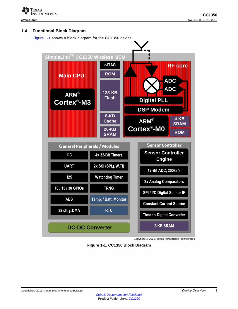
SimpleLink TM CC1350 Wireless MCU
Main CPU:
128-KBFlash
Sensor Controller
cJTAG
20-KBSRAM
ROM
ARM®
Cortex ®-M3
DC-DC Converter
RF core
ARM®
Cortex ®-M0
DSP Modem
4-KB SRAM
ROM
Sensor Controller Engine
2x Analog Comparators
12-Bit ADC, 200ks/s
Constant Current Source
SPI / I2C Digital Sensor IF
2-KB SRAM
Time-to-Digital Converter
General Peripherals / Modules
2x SSI (SPI,µW,TI)
Watchdog Timer
Temp. / Batt. Monitor
RTC
I2C
UART
I2S
10 / 15 / 30 GPIOs
AES
32 ch. PDMA
ADC
ADC
Digital PLL
TRNG
8-KBCache
4x 32-Bit Timers
Copyright © 2016, Texas Instruments Incorporated
3
CC1350www.ti.com SWRS183 –JUNE 2016
Submit Documentation FeedbackProduct Folder Links: CC1350
Device OverviewCopyright © 2016, Texas Instruments Incorporated
1.4 Functional Block DiagramFigure 1-1 shows a block diagram for the CC1350 device.
Figure 1-1. CC1350 Block Diagram
4
CC1350SWRS183 –JUNE 2016 www.ti.com
Submit Documentation FeedbackProduct Folder Links: CC1350
Revision History Copyright © 2016, Texas Instruments Incorporated
Table of Contents1 Device Overview ......................................... 1
1.1 Features .............................................. 11.2 Applications........................................... 21.3 Description............................................ 21.4 Functional Block Diagram ............................ 3
2 Revision History ......................................... 43 Device Comparison ..................................... 5
3.1 Related Products ..................................... 54 Terminal Configuration and Functions.............. 6
4.1 Pin Diagram – RGZ Package ........................ 64.2 Signal Descriptions – RGZ Package ................. 7
5 Specifications ............................................ 95.1 Absolute Maximum Ratings .......................... 95.2 ESD Ratings.......................................... 95.3 Recommended Operating Conditions ................ 95.4 Power Consumption Summary...................... 105.5 RF Characteristics .................................. 115.6 Receive (RX) Parameters, Sub-1 GHz ............. 115.7 Transmit (TX) Parameters Sub-1 GHz.............. 135.8 1-Mbps GFSK (Bluetooth low energy) – RX ........ 145.9 1-Mbps GFSK (Bluetooth low energy) – TX ........ 155.10 PLL Parameters..................................... 155.11 Thermal Characteristics ............................. 165.12 Timing and Switching Characteristics ............... 165.13 Typical Characteristics .............................. 23
6 Detailed Description ................................... 316.1 Overview ............................................ 31
6.2 Main CPU ........................................... 316.3 RF Core ............................................. 326.4 Sensor Controller ................................... 336.5 Memory.............................................. 346.6 Debug ............................................... 346.7 Power Management................................. 356.8 Clock Systems ...................................... 366.9 General Peripherals and Modules .................. 366.10 System Architecture................................. 37
7 Application, Implementation, and Layout ......... 387.1 Simplelink CC1350 LaunchPad Bluetooth and Sub-
1 GHz Long Range Wireless Development Kit ..... 388 Device and Documentation Support ............... 39
8.1 Device Nomenclature ............................... 398.2 Tools and Software ................................. 408.3 Documentation Support ............................. 418.4 Texas Instruments Low-Power RF Website ........ 418.5 Low-Power RF eNewsletter ......................... 418.6 Additional Information ............................... 418.7 Community Resources .............................. 428.8 Trademarks.......................................... 428.9 Electrostatic Discharge Caution..................... 428.10 Export Control Notice ............................... 428.11 Glossary ............................................. 43
9 Mechanical Packaging and OrderableInformation .............................................. 439.1 Packaging Information .............................. 43
2 Revision HistoryDATE REVISION NOTESJune 2016 SWRS183* Initial Release
5
CC1350www.ti.com SWRS183 –JUNE 2016
Submit Documentation FeedbackProduct Folder Links: CC1350
Device ComparisonCopyright © 2016, Texas Instruments Incorporated
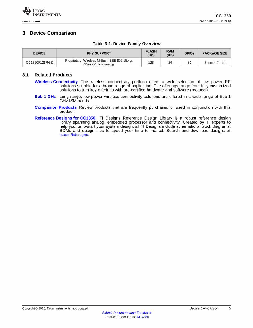
3 Device Comparison
Table 3-1. Device Family Overview
DEVICE PHY SUPPORT FLASH(KB)
RAM(KB) GPIOs PACKAGE SIZE
CC1350F128RGZ Proprietary, Wireless M-Bus, IEEE 802.15.4g,Bluetooth low energy 128 20 30 7 mm × 7 mm
3.1 Related ProductsWireless Connectivity The wireless connectivity portfolio offers a wide selection of low power RF
solutions suitable for a broad range of application. The offerings range from fully customizedsolutions to turn key offerings with pre-certified hardware and software (protocol).
Sub-1 GHz Long-range, low power wireless connectivity solutions are offered in a wide range of Sub-1GHz ISM bands.
Companion Products Review products that are frequently purchased or used in conjunction with thisproduct.
Reference Designs for CC1350 TI Designs Reference Design Library is a robust reference designlibrary spanning analog, embedded processor and connectivity. Created by TI experts tohelp you jump-start your system design, all TI Designs include schematic or block diagrams,BOMs and design files to speed your time to market. Search and download designs atti.com/tidesigns.

40
39
DIO_24
38
37
21
22
23
24
DC
DC
_SW
3334
RE
SE
T_N
35
DIO
_23
36
X32
K_Q
2
4X
32K
_Q1
3
RF
_N2
RF
_P1
DIO
_21
32
DIO
_20
31
DIO
_19
30
DIO
_18
29
5
DIO
_16
DIO
_27 8
28 27 26
JTA
G_T
CK
C25
9 10 11 12
CC13xxVQFN48 7x7
DCDC
41
42
43
44
20 DIO_14
19 DIO_13
18
17
VDDR 45
46
47
VDDR_RF 48
16
15
14
13D
IO_1
7
DIO
_16
VD
DS
_DC
DC
DIO_25
DIO_11
DIO_12
VDDS2
DIO_10
DIO_9
DIO
_5
DIO
_6
DIO
_7
DIO
_3
DIO
_4X24M_N
X24M_P DIO_8
DIO_27
VDDS3
DCOUPL
JTAG_TMSC
DIO_28
DIO_26
VDDS
RX
_TX
DIO_29
DIO_15
DIO
_22
DIO_30
6
CC1350SWRS183 –JUNE 2016 www.ti.com
Submit Documentation FeedbackProduct Folder Links: CC1350
Terminal Configuration and Functions Copyright © 2016, Texas Instruments Incorporated
4 Terminal Configuration and Functions
4.1 Pin Diagram – RGZ Package
Figure 4-1. RGZ (7-mm × 7-mm) Pinout, 0.5-mm Pitch
I/O pins marked in Figure 4-1 in bold have high drive capabilities; they are the following:• Pin 10, DIO_5• Pin 11, DIO_6• Pin 12, DIO_7• Pin 24, JTAG_TMSC• Pin 26, DIO_16• Pin 27, DIO_17
I/O pins marked in Figure 4-1 in italics have analog capabilities.• Pin 36, DIO_23• Pin 37, DIO_24• Pin 38, DIO_25• Pin 39, DIO_26• Pin 40, DIO_27• Pin 41, DIO_28• Pin 42, DIO_29• Pin 43, DIO_30
7
CC1350www.ti.com SWRS183 –JUNE 2016
Submit Documentation FeedbackProduct Folder Links: CC1350
Terminal Configuration and FunctionsCopyright © 2016, Texas Instruments Incorporated
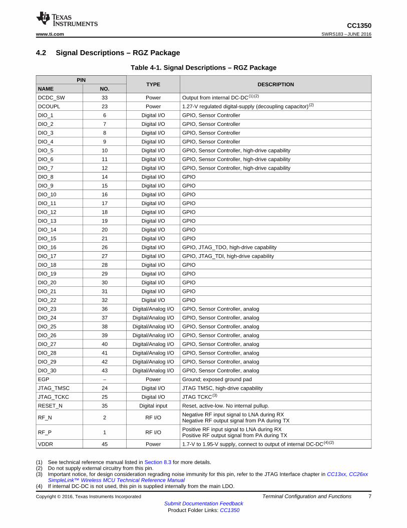
(1) See technical reference manual listed in Section 8.3 for more details.(2) Do not supply external circuitry from this pin.(3) Important notice, for design consideration regrading noise immunity for this pin, refer to the JTAG Interface chapter in CC13xx, CC26xx
SimpleLink™ Wireless MCU Technical Reference Manual(4) If internal DC-DC is not used, this pin is supplied internally from the main LDO.
4.2 Signal Descriptions – RGZ Package
Table 4-1. Signal Descriptions – RGZ Package
PINTYPE DESCRIPTION
NAME NO.DCDC_SW 33 Power Output from internal DC-DC (1) (2)
DCOUPL 23 Power 1.27-V regulated digital-supply (decoupling capacitor) (2)
DIO_1 6 Digital I/O GPIO, Sensor ControllerDIO_2 7 Digital I/O GPIO, Sensor ControllerDIO_3 8 Digital I/O GPIO, Sensor ControllerDIO_4 9 Digital I/O GPIO, Sensor ControllerDIO_5 10 Digital I/O GPIO, Sensor Controller, high-drive capabilityDIO_6 11 Digital I/O GPIO, Sensor Controller, high-drive capabilityDIO_7 12 Digital I/O GPIO, Sensor Controller, high-drive capabilityDIO_8 14 Digital I/O GPIODIO_9 15 Digital I/O GPIODIO_10 16 Digital I/O GPIODIO_11 17 Digital I/O GPIODIO_12 18 Digital I/O GPIODIO_13 19 Digital I/O GPIODIO_14 20 Digital I/O GPIODIO_15 21 Digital I/O GPIODIO_16 26 Digital I/O GPIO, JTAG_TDO, high-drive capabilityDIO_17 27 Digital I/O GPIO, JTAG_TDI, high-drive capabilityDIO_18 28 Digital I/O GPIODIO_19 29 Digital I/O GPIODIO_20 30 Digital I/O GPIODIO_21 31 Digital I/O GPIODIO_22 32 Digital I/O GPIODIO_23 36 Digital/Analog I/O GPIO, Sensor Controller, analogDIO_24 37 Digital/Analog I/O GPIO, Sensor Controller, analogDIO_25 38 Digital/Analog I/O GPIO, Sensor Controller, analogDIO_26 39 Digital/Analog I/O GPIO, Sensor Controller, analogDIO_27 40 Digital/Analog I/O GPIO, Sensor Controller, analogDIO_28 41 Digital/Analog I/O GPIO, Sensor Controller, analogDIO_29 42 Digital/Analog I/O GPIO, Sensor Controller, analogDIO_30 43 Digital/Analog I/O GPIO, Sensor Controller, analogEGP – Power Ground; exposed ground padJTAG_TMSC 24 Digital I/O JTAG TMSC, high-drive capabilityJTAG_TCKC 25 Digital I/O JTAG TCKC (3)
RESET_N 35 Digital input Reset, active-low. No internal pullup.
RF_N 2 RF I/O Negative RF input signal to LNA during RXNegative RF output signal from PA during TX
RF_P 1 RF I/O Positive RF input signal to LNA during RXPositive RF output signal from PA during TX
VDDR 45 Power 1.7-V to 1.95-V supply, connect to output of internal DC-DC (4) (2)
8
CC1350SWRS183 –JUNE 2016 www.ti.com
Submit Documentation FeedbackProduct Folder Links: CC1350
Terminal Configuration and Functions Copyright © 2016, Texas Instruments Incorporated
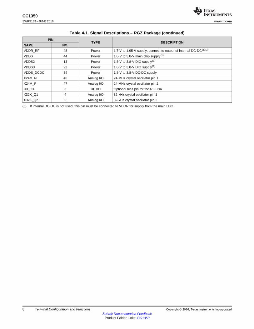
Table 4-1. Signal Descriptions – RGZ Package (continued)PIN
TYPE DESCRIPTIONNAME NO.
(5) If internal DC-DC is not used, this pin must be connected to VDDR for supply from the main LDO.
VDDR_RF 48 Power 1.7-V to 1.95-V supply, connect to output of internal DC-DC (5) (2)
VDDS 44 Power 1.8-V to 3.8-V main chip supply (1)
VDDS2 13 Power 1.8-V to 3.8-V DIO supply (1)
VDDS3 22 Power 1.8-V to 3.8-V DIO supply (1)
VDDS_DCDC 34 Power 1.8-V to 3.8-V DC-DC supplyX24M_N 46 Analog I/O 24-MHz crystal oscillator pin 1X24M_P 47 Analog I/O 24-MHz crystal oscillator pin 2RX_TX 3 RF I/O Optional bias pin for the RF LNAX32K_Q1 4 Analog I/O 32-kHz crystal oscillator pin 1X32K_Q2 5 Analog I/O 32-kHz crystal oscillator pin 2
9
CC1350www.ti.com SWRS183 –JUNE 2016
Submit Documentation FeedbackProduct Folder Links: CC1350
SpecificationsCopyright © 2016, Texas Instruments Incorporated
(1) Stresses beyond those listed under Absolute Maximum Ratings may cause permanent damage to the device. These are stress ratingsonly, and functional operation of the device at these or any other conditions beyond those indicated under Recommended OperatingConditions is not implied. Exposure to absolute-maximum-rated conditions for extended periods may affect device reliability.
(2) All voltage values are with respect to ground, unless otherwise noted.(3) VDDS2 and VDDS3 must be at the same potential as VDDS.(4) Including analog-capable DIO
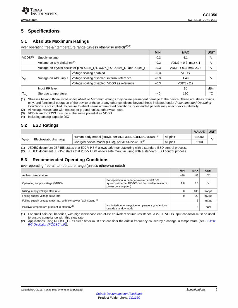
5 Specifications
5.1 Absolute Maximum Ratingsover operating free-air temperature range (unless otherwise noted) (1) (2)
MIN MAX UNITVDDS (3) Supply voltage –0.3 4.1 V
Voltage on any digital pin (4) –0.3 VDDS + 0.3, max 4.1 VVoltage on crystal oscillator pins X32K_Q1, X32K_Q2, X24M_N, and X24M_P –0.3 VDDR + 0.3, max 2.25 V
Vin Voltage on ADC inputVoltage scaling enabled –0.3 VDDS
VVoltage scaling disabled, internal reference –0.3 1.49Voltage scaling disabled, VDDS as reference –0.3 VDDS / 2.9
Input RF level 10 dBmTstg Storage temperature –40 150 °C
(1) JEDEC document JEP155 states that 500-V HBM allows safe manufacturing with a standard ESD control process.(2) JEDEC document JEP157 states that 250-V CDM allows safe manufacturing with a standard ESD control process.
5.2 ESD RatingsVALUE UNIT
VESD Electrostatic dischargeHuman body model (HBM), per ANSI/ESDA/JEDEC JS001 (1) All pins ±3000
VCharged device model (CDM), per JESD22-C101 (2) All pins ±500
(1) For small coin-cell batteries, with high worst-case end-of-life equivalent source resistance, a 22-µF VDDS input capacitor must be usedto ensure compliance with this slew rate.
(2) Applications using RCOSC_LF as sleep timer must also consider the drift in frequency caused by a change in temperature (see 32-kHzRC Oscillator (RCOSC_LF)).
5.3 Recommended Operating Conditionsover operating free-air temperature range (unless otherwise noted)
MIN MAX UNIT
Ambient temperature –40 85 °C
Operating supply voltage (VDDS)For operation in battery-powered and 3.3-Vsystems (internal DC-DC can be used to minimizepower consumption)
1.8 3.8 V
Rising supply voltage slew rate 0 100 mV/µs
Falling supply voltage slew rate 0 20 mV/µs
Falling supply voltage slew rate, with low-power flash setting (1) 3 mV/µs
Positive temperature gradient in standby (2) No limitation for negative temperature gradient, oroutside standby mode 5 °C/s
10
CC1350SWRS183 –JUNE 2016 www.ti.com
Submit Documentation FeedbackProduct Folder Links: CC1350
Specifications Copyright © 2016, Texas Instruments Incorporated
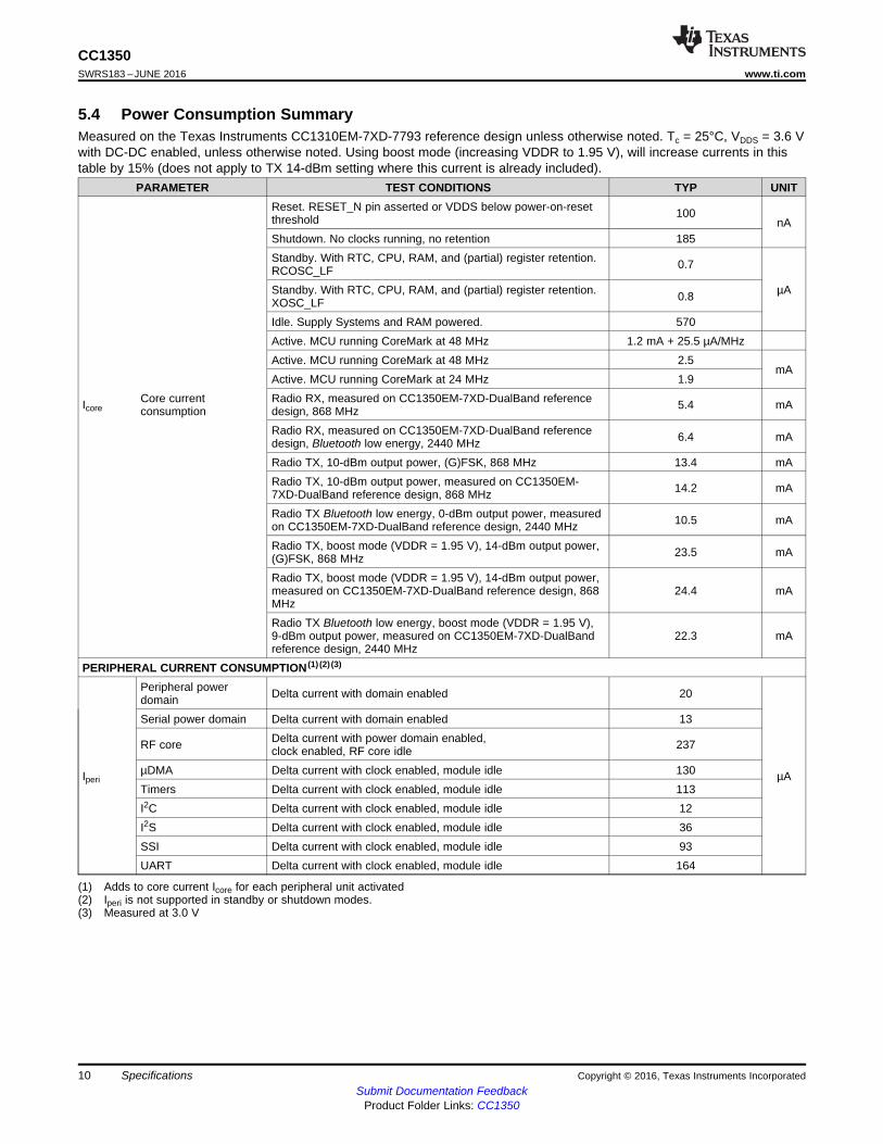
(1) Adds to core current Icore for each peripheral unit activated(2) Iperi is not supported in standby or shutdown modes.(3) Measured at 3.0 V
5.4 Power Consumption SummaryMeasured on the Texas Instruments CC1310EM-7XD-7793 reference design unless otherwise noted. Tc = 25°C, VDDS = 3.6 Vwith DC-DC enabled, unless otherwise noted. Using boost mode (increasing VDDR to 1.95 V), will increase currents in thistable by 15% (does not apply to TX 14-dBm setting where this current is already included).
PARAMETER TEST CONDITIONS TYP UNITReset. RESET_N pin asserted or VDDS below power-on-resetthreshold 100
nAShutdown. No clocks running, no retention 185Standby. With RTC, CPU, RAM, and (partial) register retention.RCOSC_LF 0.7
µAStandby. With RTC, CPU, RAM, and (partial) register retention.XOSC_LF 0.8
Idle. Supply Systems and RAM powered. 570Active. MCU running CoreMark at 48 MHz 1.2 mA + 25.5 µA/MHzActive. MCU running CoreMark at 48 MHz 2.5
mAActive. MCU running CoreMark at 24 MHz 1.9
IcoreCore currentconsumption
Radio RX, measured on CC1350EM-7XD-DualBand referencedesign, 868 MHz 5.4 mA
Radio RX, measured on CC1350EM-7XD-DualBand referencedesign, Bluetooth low energy, 2440 MHz 6.4 mA
Radio TX, 10-dBm output power, (G)FSK, 868 MHz 13.4 mARadio TX, 10-dBm output power, measured on CC1350EM-7XD-DualBand reference design, 868 MHz 14.2 mA
Radio TX Bluetooth low energy, 0-dBm output power, measuredon CC1350EM-7XD-DualBand reference design, 2440 MHz 10.5 mA
Radio TX, boost mode (VDDR = 1.95 V), 14-dBm output power,(G)FSK, 868 MHz 23.5 mA
Radio TX, boost mode (VDDR = 1.95 V), 14-dBm output power,measured on CC1350EM-7XD-DualBand reference design, 868MHz
24.4 mA
Radio TX Bluetooth low energy, boost mode (VDDR = 1.95 V),9-dBm output power, measured on CC1350EM-7XD-DualBandreference design, 2440 MHz
22.3 mA
PERIPHERAL CURRENT CONSUMPTION (1) (2) (3)
Iperi
Peripheral powerdomain Delta current with domain enabled 20
µA
Serial power domain Delta current with domain enabled 13
RF core Delta current with power domain enabled,clock enabled, RF core idle 237
µDMA Delta current with clock enabled, module idle 130Timers Delta current with clock enabled, module idle 113I2C Delta current with clock enabled, module idle 12I2S Delta current with clock enabled, module idle 36SSI Delta current with clock enabled, module idle 93UART Delta current with clock enabled, module idle 164

11
CC1350www.ti.com SWRS183 –JUNE 2016
Submit Documentation FeedbackProduct Folder Links: CC1350
SpecificationsCopyright © 2016, Texas Instruments Incorporated
(1) For more information, refer to CC1350 SimpleLink Wireless MCU Silicon Errata.
5.5 RF Characteristicsover operating free-air temperature range (unless otherwise noted)
PARAMETER MIN TYP MAX UNIT
Frequency bands (1)
(287) (351)
MHz
(359) (439)(431) (527)(718) (878)
861 10542152 2635
5.6 Receive (RX) Parameters, Sub-1 GHzMeasured on the Texas Instruments CC1350_7XD-Dual Band reference design with Tc = 25°C, VDDS = 3.0 V, DC-DCenabled, fRF = 868 MHz, unless otherwise noted. All measurements are performed at the antenna input with a combined RXand TX path.
PARAMETER TEST CONDITIONS MIN TYP MAX UNITData rate 50 kbps
Data rate offset tolerance,IEEE 802.15.4g PHY
50 kbps, GFSK, 25-kHz deviation, 100-kHz RXbandwidth (same modulation format as IEEE 802.15.4gmandatory mode), BER = 10–3
1600 ppm
Data rate step size 1.5 bpsDigital channel filter programmablebandwidth Using VCO divide by 5 setting 40 4000 kHz
Receiver sensitivity, 50 kbps50 kbps, GFSK, 25-kHz deviation, 100-kHz RXbandwidth (same modulation format as IEEE 802.15.4gmandatory mode), BER = 10–2 868 MHz and 915 MHz
-109 dBm
Receiver sensitivity, 50 kbps
50 kbps, GFSK, 25-kHz deviation, 100-kHz RXbandwidth (same modulation format as IEEE 802.15.4gmandatory mode), BER = 10–2 868 MHz and 915 MHZ.Measured on CC1310EM-7XD-7793
-110 dBm
Receiver saturation50 kbps, GFSK, 25-kHz deviation, 100-kHz RXbandwidth (same modulation format as IEEE 802.15.4gmandatory mode), BER = 10–2
10 dBm
Selectivity, ±200 kHz, 50 kbps
Wanted signal 3 dB above sensitivity limit. 50 kbps,GFSK, 25-kHz deviation, 100-kHz RX bandwidth (samemodulation format as IEEE 802.15.4g mandatorymode), BER = 10–2
44, 47 dB
Selectivity, ±400 kHz, 50 kbps
Wanted signal 3 dB above sensitivity limit. 50 kbps,GFSK, 25-kHz deviation, 100-kHz RX bandwidth (samemodulation format as IEEE 802.15.4g mandatorymode), BER = 10–2
48, 53 dB
Blocking ±1 MHz, 50 kbps
Wanted signal 3 dB above sensitivity limit. 50 kbps,GFSK, 25-kHz deviation, 100-kHz RX bandwidth (samemodulation format as IEEE 802.15.4g mandatorymode), BER = 10–2
59, 62 dB
Blocking ±2 MHz, 50 kbps
Wanted signal 3 dB above sensitivity limit. 50 kbps,GFSK, 25-kHz deviation, 100-kHz RX bandwidth (samemodulation format as IEEE 802.15.4g mandatorymode), BER = 10–2
64, 65 dB
Blocking ±5 MHz, 50 kbps
Wanted signal 3 dB above sensitivity limit. 50 kbps,GFSK, 25-kHz deviation, 100-kHz RX bandwidth (samemodulation format as IEEE 802.15.4g mandatorymode), BER = 10–2
67, 68 dB
Blocking ±10 MHz, 50 kbps
Wanted signal 3 dB above sensitivity limit. 50 kbps,GFSK, 25-kHz deviation, 100-kHz RX bandwidth (samemodulation format as IEEE 802.15.4g mandatorymode), BER = 10–2
76, 76 dB

12
CC1350SWRS183 –JUNE 2016 www.ti.com
Submit Documentation FeedbackProduct Folder Links: CC1350
Specifications Copyright © 2016, Texas Instruments Incorporated
Receive (RX) Parameters, Sub-1 GHz (continued)Measured on the Texas Instruments CC1350_7XD-Dual Band reference design with Tc = 25°C, VDDS = 3.0 V, DC-DCenabled, fRF = 868 MHz, unless otherwise noted. All measurements are performed at the antenna input with a combined RXand TX path.
PARAMETER TEST CONDITIONS MIN TYP MAX UNITSpurious emissions 1 GHz to 13 GHz(VCO leakage at 3.5 GHz) and 30 MHzto 1 GHz
Radiated emissions measured according to ETSI EN300 220 –70 dBm
Image rejection (image compensationenabled, the image compensation iscalibrated in production)
Wanted signal 3 dB above sensitivity limit. 50 kbps,GFSK, 25-kHz deviation, 100-kHz RX bandwidth (samemodulation format as IEEE 802.15.4g mandatorymode), BER = 10–2
44 dB
RSSI dynamic range
50 kbps, GFSK, 25-kHz deviation, 100-kHz RXbandwidth (same modulation format as IEEE 802.15.4gmandatory mode). Starting from the sensitivity limit. Thisrange will give an accuracy of ±2 dB.
95 dB
RSSI accuracy
50 kbps, GFSK, 25-kHz deviation, 100-kHz RXbandwidth (same modulation format as IEEE 802.15.4gmandatory mode). Starting from the sensitivity limitacross the given dynamic range.
±2 dB
Receiver sensitivity, long-range mode625 bps
10 ksps, GFSK, 5-kHz deviation, FEC (half rate),DSSS = 8, 40-kHz RX bandwidth, BER = 10–2. 868MHz and 915 MHZ.
–124 dBm
Selectivity, ±100 kHz, long-range mode625 bps
Wanted signal 3 dB above sensitivity limit. 10 ksps,GFSK, 5-kHz deviation, FEC (half rate), DSSS = 8,40-kHz RX bandwidth, BER = 10–2
56, 56 dB
Selectivity, ±200 kHz, long-range mode625 bps
Wanted signal 3 dB above sensitivity limit. 10 ksps,GFSK, 5-kHz deviation, FEC (half rate), DSSS = 8,40-kHz RX bandwidth, BER = 10–2
62, 65 dB
Blocking ±1 MHz, long-range mode625 bps
Wanted signal 3 dB above sensitivity limit. 10 ksps,GFSK, 5-kHz deviation, FEC (half rate), DSSS = 8,40-kHz RX bandwidth, BER = 10–2
73, 77 dB
Blocking ±2 MHz, long-range mode625 bps
Wanted signal 3 dB above sensitivity limit. 10 ksps,GFSK, 5-kHz deviation, FEC (half rate), DSSS = 8,40-kHz RX bandwidth, BER = 10–2
79, 79 dB
Blocking ±10 MHz, long-range mode625 bps
Wanted signal 3 dB above sensitivity limit. 10 ksps,GFSK, 5-kHz deviation, FEC (half rate), DSSS = 8,40-kHz RX bandwidth, BER = 10–2
91, 91 dB

13
CC1350www.ti.com SWRS183 –JUNE 2016
Submit Documentation FeedbackProduct Folder Links: CC1350
SpecificationsCopyright © 2016, Texas Instruments Incorporated
(1) Suitable for systems targeting compliance with EN 300 220, EN 54-25, EN 303 131, EN 303 204, FCC CFR47 Part 15, ARIB STD-T108.
5.7 Transmit (TX) Parameters Sub-1 GHzMeasured on the Texas Instruments CC1310EM-7XD-7793 reference design with Tc = 25°C, VDDS = 3.0 V, DC-DC enabled,fRF = 868 MHz, unless otherwise noted. All measurements are performed at the antenna input with a combined RX and TXpath.
PARAMETER TEST CONDITIONS MIN TYP MAX UNIT
Maximum output power, boost modeVDDR = 1.95 VMinimum VDDS for boost mode is 2.1 V868 MHz and 915 MHz
14 dBm
Maximum output power 868 MHz and 915 MHz 12 dBmOutput power programmable range 24 dBOutput power variation Tested at +10-dBm setting ±0.9 dBOutput power variation, boost mode +14 dBm ±0.5 dB
Spurious emissions(excluding harmonics) (1)
30 MHz to 1 GHz
Transmitting +14 dBmETSI restricted bands <–59 dBm
Transmitting +14 dBmoutside ETSI restricted bands <–51 dBm
1 GHz to 12.75 GHz Transmitting +14 dBmmeasured in 1-MHz bandwidth (ETSI) <–37 dBm
Harmonics
Second harmonic Transmitting +14 dBm, conducted868 MHz, 915 MHz –52, –55 dBm
Third harmonic Transmitting +14 dBm, conducted868 MHz, 915 MHz –58, –55 dBm
Fourth harmonic Transmitting +14 dBm, conducted868 MHz, 915 MHz –56, –56 dBm
Spurious emissions out-of-band, 915 MHz (1)
30 MHz to 88 MHz(within FCC restricted bands) Transmitting +14 dBm, conducted <–66 dBm
88 MHz to 216 MHz(within FCC restricted bands) Transmitting +14 dBm, conducted <–65 dBm
216 MHz to 960 MHz(within FCC restricted bands) Transmitting +14 dBm, conducted <–65 dBm
960 MHz to 2390 MHz andabove 2483.5 MHz (withinFCC restricted band)
Transmitting +14 dBm, conducted <–52 dBm
1 GHz to 12.75 GHz(outside FCC restrictedbands)
Transmitting +14 dBm, conducted <–43 dBm
Spurious emissions out-of-band, 920.6 MHz (1)
Below 710 MHz(ARIB T-108) Transmitting +14 dBm, conducted <–50 dBm
710 MHz to 900 MHz(ARIB T-108) Transmitting +14 dBm, conducted <–60 dBm
900 MHz to 915 MHz(ARIB T-108) Transmitting +14 dBm, conducted <–57 dBm
930 MHz to 1000 MHz(ARIB T-108) Transmitting +14 dBm, conducted <–57 dBm
1000 MHz to 1215 MHz(ARIB T-108) Transmitting +14 dBm, conducted <–59 dBm
Above 1215 MHz(ARIB T-108) Transmitting +14 dBm, conducted <–45 dBm
14
CC1350SWRS183 –JUNE 2016 www.ti.com
Submit Documentation FeedbackProduct Folder Links: CC1350
Specifications Copyright © 2016, Texas Instruments Incorporated
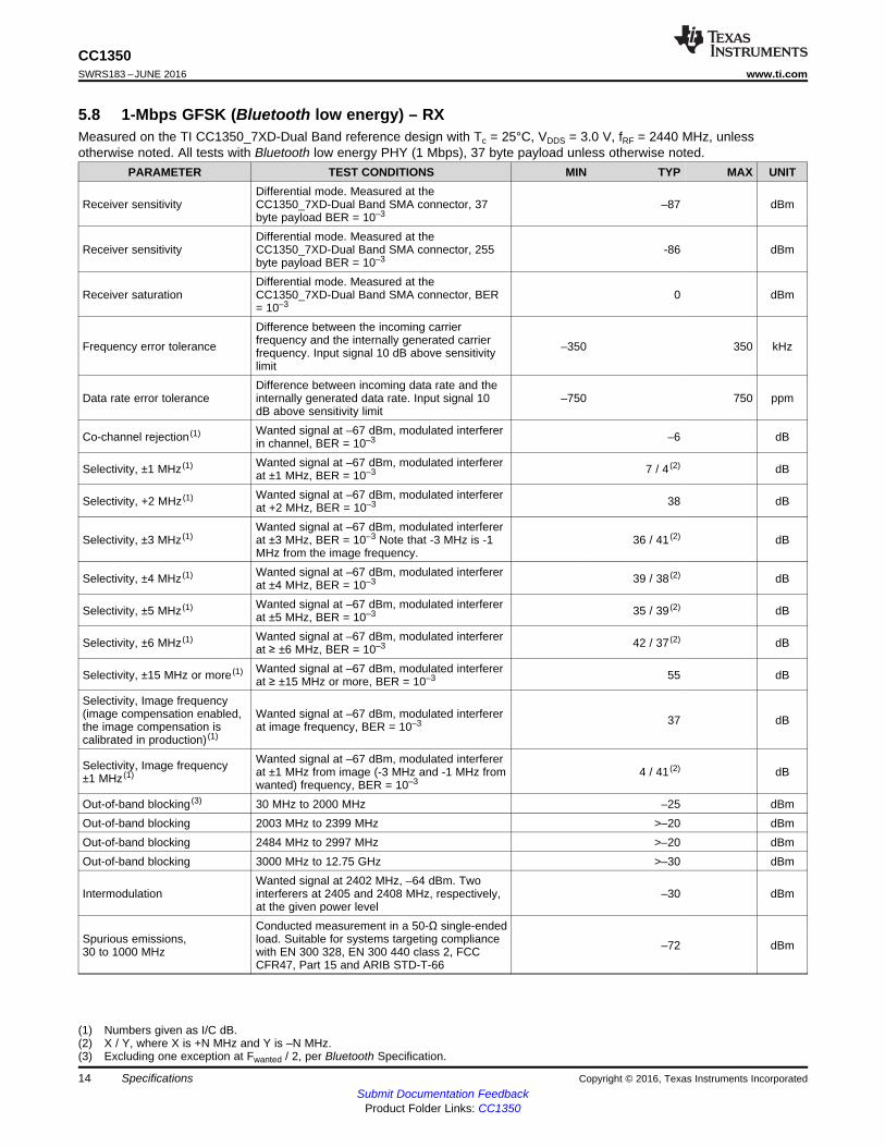
(1) Numbers given as I/C dB.(2) X / Y, where X is +N MHz and Y is –N MHz.(3) Excluding one exception at Fwanted / 2, per Bluetooth Specification.
5.8 1-Mbps GFSK (Bluetooth low energy) – RXMeasured on the TI CC1350_7XD-Dual Band reference design with Tc = 25°C, VDDS = 3.0 V, fRF = 2440 MHz, unlessotherwise noted. All tests with Bluetooth low energy PHY (1 Mbps), 37 byte payload unless otherwise noted.
PARAMETER TEST CONDITIONS MIN TYP MAX UNIT
Receiver sensitivityDifferential mode. Measured at theCC1350_7XD-Dual Band SMA connector, 37byte payload BER = 10–3
–87 dBm
Receiver sensitivityDifferential mode. Measured at theCC1350_7XD-Dual Band SMA connector, 255byte payload BER = 10–3
-86 dBm
Receiver saturationDifferential mode. Measured at theCC1350_7XD-Dual Band SMA connector, BER= 10–3
0 dBm
Frequency error tolerance
Difference between the incoming carrierfrequency and the internally generated carrierfrequency. Input signal 10 dB above sensitivitylimit
–350 350 kHz
Data rate error toleranceDifference between incoming data rate and theinternally generated data rate. Input signal 10dB above sensitivity limit
–750 750 ppm
Co-channel rejection (1) Wanted signal at –67 dBm, modulated interfererin channel, BER = 10–3 –6 dB
Selectivity, ±1 MHz (1) Wanted signal at –67 dBm, modulated interfererat ±1 MHz, BER = 10–3 7 / 4 (2) dB
Selectivity, +2 MHz (1) Wanted signal at –67 dBm, modulated interfererat +2 MHz, BER = 10–3 38 dB
Selectivity, ±3 MHz (1)Wanted signal at –67 dBm, modulated interfererat ±3 MHz, BER = 10–3 Note that -3 MHz is -1MHz from the image frequency.
36 / 41 (2) dB
Selectivity, ±4 MHz (1) Wanted signal at –67 dBm, modulated interfererat ±4 MHz, BER = 10–3 39 / 38 (2) dB
Selectivity, ±5 MHz (1) Wanted signal at –67 dBm, modulated interfererat ±5 MHz, BER = 10–3 35 / 39 (2) dB
Selectivity, ±6 MHz (1) Wanted signal at –67 dBm, modulated interfererat ≥ ±6 MHz, BER = 10–3 42 / 37 (2) dB
Selectivity, ±15 MHz or more (1) Wanted signal at –67 dBm, modulated interfererat ≥ ±15 MHz or more, BER = 10–3 55 dB
Selectivity, Image frequency(image compensation enabled,the image compensation iscalibrated in production) (1)
Wanted signal at –67 dBm, modulated interfererat image frequency, BER = 10–3 37 dB
Selectivity, Image frequency±1 MHz (1)
Wanted signal at –67 dBm, modulated interfererat ±1 MHz from image (-3 MHz and -1 MHz fromwanted) frequency, BER = 10–3
4 / 41 (2) dB
Out-of-band blocking (3) 30 MHz to 2000 MHz –25 dBmOut-of-band blocking 2003 MHz to 2399 MHz >–20 dBmOut-of-band blocking 2484 MHz to 2997 MHz >–20 dBmOut-of-band blocking 3000 MHz to 12.75 GHz >–30 dBm
IntermodulationWanted signal at 2402 MHz, –64 dBm. Twointerferers at 2405 and 2408 MHz, respectively,at the given power level
–30 dBm
Spurious emissions,30 to 1000 MHz
Conducted measurement in a 50-Ω single-endedload. Suitable for systems targeting compliancewith EN 300 328, EN 300 440 class 2, FCCCFR47, Part 15 and ARIB STD-T-66
–72 dBm

15
CC1350www.ti.com SWRS183 –JUNE 2016
Submit Documentation FeedbackProduct Folder Links: CC1350
SpecificationsCopyright © 2016, Texas Instruments Incorporated
1-Mbps GFSK (Bluetooth low energy) – RX (continued)Measured on the TI CC1350_7XD-Dual Band reference design with Tc = 25°C, VDDS = 3.0 V, fRF = 2440 MHz, unlessotherwise noted. All tests with Bluetooth low energy PHY (1 Mbps), 37 byte payload unless otherwise noted.
PARAMETER TEST CONDITIONS MIN TYP MAX UNIT
Spurious emissions,1 to 12.75 GHz
Conducted measurement in a 50-Ω single-endedload. Suitable for systems targeting compliancewith EN 300 328, EN 300 440 class 2, FCCCFR47, Part 15 and ARIB STD-T-66
–65 dBm
RSSI dynamic range 70 dBRSSI accuracy ±4 dB
(1) Suitable for systems targeting compliance with worldwide radio-frequency regulations ETSI EN 300 328 and EN 300 440 Class 2(Europe), FCC CFR47 Part 15 (US), and ARIB STD-T66 (Japan).
5.9 1-Mbps GFSK (Bluetooth low energy) – TXMeasured on the TI CC1350_7XD-Dual Band reference design with Tc = 25°C, VDDS = 3.0 V, fRF = 2440 MHz, unlessotherwise noted.
PARAMETER TEST CONDITIONS MIN TYP MAX UNIT
Output power, boost mode
Differential mode, delivered to a single-ended 50-Ω loadthrough a balun.VDDR = 1.95 VMinimum VDDS for boost mode is 2.1 V.
9 dBm
Output power Differential mode, delivered to a single-ended 50-Ω loadthrough a balun. 5 dBm
Output power, lowest setting Delivered to a single-ended 50-Ω load through a balun -21 dBm
Spurious emission conductedmeasurement (1)
f < 1 GHz, outside restricted bands –59
dBmf < 1 GHz, restricted bands ETSI -55f < 1 GHz, restricted bands FCC –61f > 1 GHz, including harmonics –47
5.10 PLL ParametersMeasured on the Texas Instruments CC1310EM-7XD-7793 reference design with Tc = 25°C, VDDS = 3.0 V
PARAMETER TEST CONDITIONS MIN TYP MAX UNIT
Phase noise in the 868-MHz band
±100-kHz offset –101
dBc/Hz
±200-kHz offset –108±400-kHz offset –115±1000-kHz offset –124±2000-kHz offset –131±10000-kHz offset –140
Phase noise in the 915-MHz band
±100-kHz offset –98
dBc/Hz
±200-kHz offset –106±400-kHz offset –114±1000-kHz offset –122±2000-kHz offset –130±10000-kHz offset –140
16
CC1350SWRS183 –JUNE 2016 www.ti.com
Submit Documentation FeedbackProduct Folder Links: CC1350
Specifications Copyright © 2016, Texas Instruments Incorporated
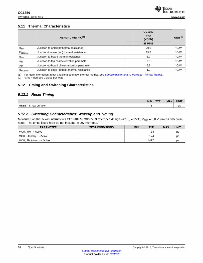
(1) For more information about traditional and new thermal metrics, see Semiconductor and IC Package Thermal Metrics.(2) °C/W = degrees Celsius per watt.
5.11 Thermal Characteristics
THERMAL METRIC (1)
CC1350
UNIT (2)RGZ(VQFN)48 PINS
RθJA Junction-to-ambient thermal resistance 29.6 °C/WRθJC(top) Junction-to-case (top) thermal resistance 15.7 °C/WRθJB Junction-to-board thermal resistance 6.2 °C/WψJT Junction-to-top characterization parameter 0.3 °C/WψJB Junction-to-board characterization parameter 6.2 °C/WRθJC(bot) Junction-to-case (bottom) thermal resistance 1.9 °C/W
5.12 Timing and Switching Characteristics
5.12.1 Reset Timing
MIN TYP MAX UNITRESET_N low duration 1 µs
5.12.2 Switching Characteristics: Wakeup and TimingMeasured on the Texas Instruments CC1310EM-7XD-7793 reference design with Tc = 25°C, VDDS = 3.0 V, unless otherwisenoted. The times listed here do not include RTOS overhead.
PARAMETER TEST CONDITIONS MIN TYP MAX UNITMCU, Idle → Active 14 µsMCU, Standby → Active 174 µsMCU, Shutdown → Active 1097 µs
17
CC1350www.ti.com SWRS183 –JUNE 2016
Submit Documentation FeedbackProduct Folder Links: CC1350
SpecificationsCopyright © 2016, Texas Instruments Incorporated
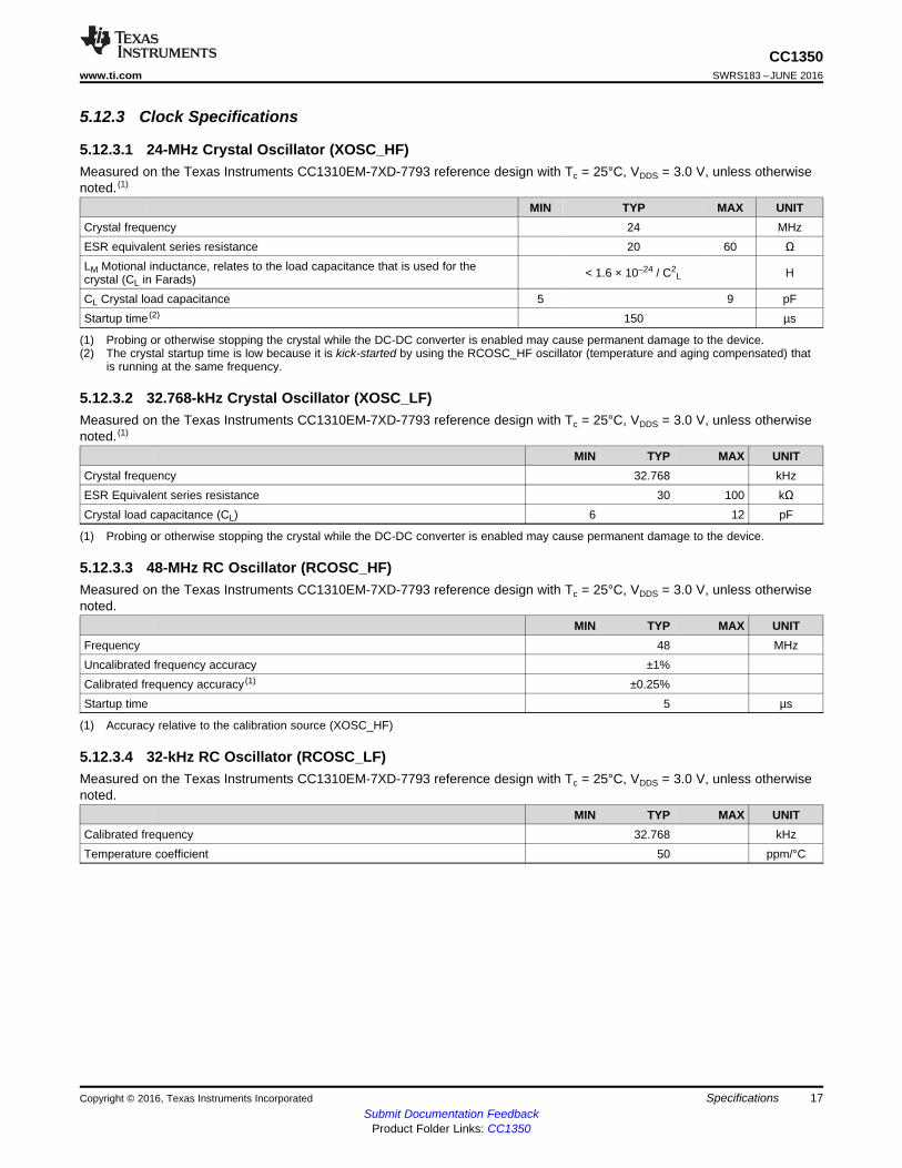
5.12.3 Clock Specifications
5.12.3.1 24-MHz Crystal Oscillator (XOSC_HF)
(1) Probing or otherwise stopping the crystal while the DC-DC converter is enabled may cause permanent damage to the device.(2) The crystal startup time is low because it is kick-started by using the RCOSC_HF oscillator (temperature and aging compensated) that
is running at the same frequency.
Measured on the Texas Instruments CC1310EM-7XD-7793 reference design with Tc = 25°C, VDDS = 3.0 V, unless otherwisenoted. (1)
MIN TYP MAX UNITCrystal frequency 24 MHzESR equivalent series resistance 20 60 ΩLM Motional inductance, relates to the load capacitance that is used for thecrystal (CL in Farads) < 1.6 × 10⁻²⁴ / C2
L H
CL Crystal load capacitance 5 9 pFStartup time (2) 150 µs
5.12.3.2 32.768-kHz Crystal Oscillator (XOSC_LF)
(1) Probing or otherwise stopping the crystal while the DC-DC converter is enabled may cause permanent damage to the device.
Measured on the Texas Instruments CC1310EM-7XD-7793 reference design with Tc = 25°C, VDDS = 3.0 V, unless otherwisenoted. (1)
MIN TYP MAX UNITCrystal frequency 32.768 kHzESR Equivalent series resistance 30 100 kΩCrystal load capacitance (CL) 6 12 pF
5.12.3.3 48-MHz RC Oscillator (RCOSC_HF)
(1) Accuracy relative to the calibration source (XOSC_HF)
Measured on the Texas Instruments CC1310EM-7XD-7793 reference design with Tc = 25°C, VDDS = 3.0 V, unless otherwisenoted.
MIN TYP MAX UNITFrequency 48 MHzUncalibrated frequency accuracy ±1%Calibrated frequency accuracy (1) ±0.25%Startup time 5 µs
5.12.3.4 32-kHz RC Oscillator (RCOSC_LF)Measured on the Texas Instruments CC1310EM-7XD-7793 reference design with Tc = 25°C, VDDS = 3.0 V, unless otherwisenoted.
MIN TYP MAX UNITCalibrated frequency 32.768 kHzTemperature coefficient 50 ppm/°C
18
CC1350SWRS183 –JUNE 2016 www.ti.com
Submit Documentation FeedbackProduct Folder Links: CC1350
Specifications Copyright © 2016, Texas Instruments Incorporated
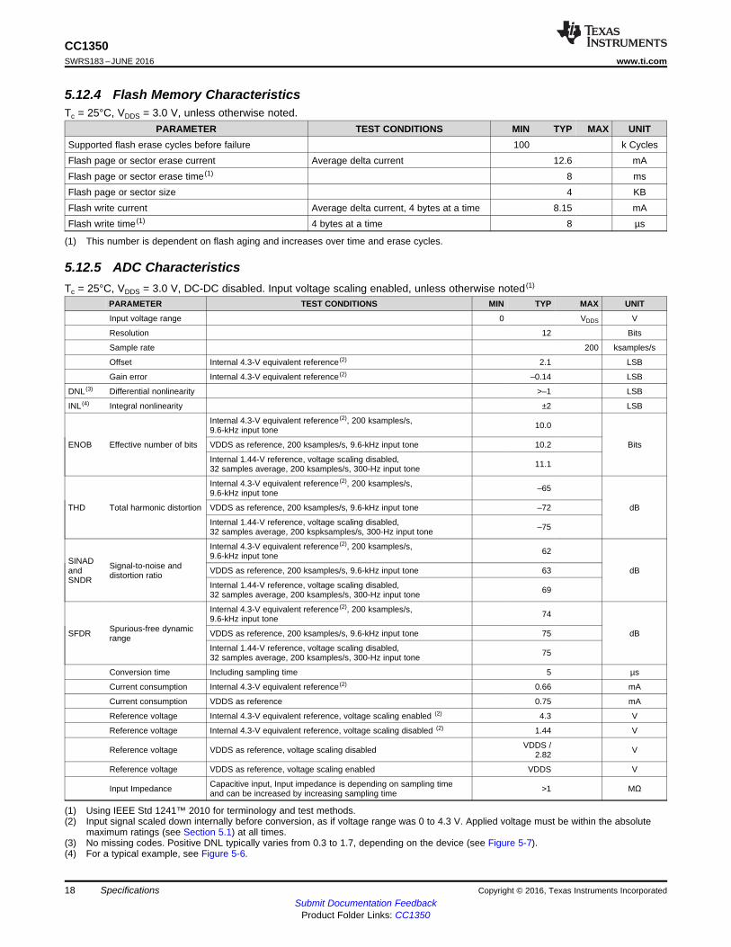
5.12.4 Flash Memory Characteristics
(1) This number is dependent on flash aging and increases over time and erase cycles.
Tc = 25°C, VDDS = 3.0 V, unless otherwise noted.PARAMETER TEST CONDITIONS MIN TYP MAX UNIT
Supported flash erase cycles before failure 100 k CyclesFlash page or sector erase current Average delta current 12.6 mAFlash page or sector erase time (1) 8 msFlash page or sector size 4 KBFlash write current Average delta current, 4 bytes at a time 8.15 mAFlash write time (1) 4 bytes at a time 8 µs
5.12.5 ADC Characteristics
(1) Using IEEE Std 1241™ 2010 for terminology and test methods.(2) Input signal scaled down internally before conversion, as if voltage range was 0 to 4.3 V. Applied voltage must be within the absolute
maximum ratings (see Section 5.1) at all times.(3) No missing codes. Positive DNL typically varies from 0.3 to 1.7, depending on the device (see Figure 5-7).(4) For a typical example, see Figure 5-6.
Tc = 25°C, VDDS = 3.0 V, DC-DC disabled. Input voltage scaling enabled, unless otherwise noted (1)
PARAMETER TEST CONDITIONS MIN TYP MAX UNIT
Input voltage range 0 VDDS V
Resolution 12 Bits
Sample rate 200 ksamples/s
Offset Internal 4.3-V equivalent reference (2) 2.1 LSB
Gain error Internal 4.3-V equivalent reference (2) –0.14 LSB
DNL (3) Differential nonlinearity >–1 LSB
INL (4) Integral nonlinearity ±2 LSB
ENOB Effective number of bits
Internal 4.3-V equivalent reference (2), 200 ksamples/s,9.6-kHz input tone 10.0
BitsVDDS as reference, 200 ksamples/s, 9.6-kHz input tone 10.2
Internal 1.44-V reference, voltage scaling disabled,32 samples average, 200 ksamples/s, 300-Hz input tone 11.1
THD Total harmonic distortion
Internal 4.3-V equivalent reference (2), 200 ksamples/s,9.6-kHz input tone –65
dBVDDS as reference, 200 ksamples/s, 9.6-kHz input tone –72
Internal 1.44-V reference, voltage scaling disabled,32 samples average, 200 kspksamples/s, 300-Hz input tone –75
SINADandSNDR
Signal-to-noise anddistortion ratio
Internal 4.3-V equivalent reference (2), 200 ksamples/s,9.6-kHz input tone 62
dBVDDS as reference, 200 ksamples/s, 9.6-kHz input tone 63
Internal 1.44-V reference, voltage scaling disabled,32 samples average, 200 ksamples/s, 300-Hz input tone 69
SFDR Spurious-free dynamicrange
Internal 4.3-V equivalent reference (2), 200 ksamples/s,9.6-kHz input tone 74
dBVDDS as reference, 200 ksamples/s, 9.6-kHz input tone 75
Internal 1.44-V reference, voltage scaling disabled,32 samples average, 200 ksamples/s, 300-Hz input tone 75
Conversion time Including sampling time 5 µs
Current consumption Internal 4.3-V equivalent reference (2) 0.66 mA
Current consumption VDDS as reference 0.75 mA
Reference voltage Internal 4.3-V equivalent reference, voltage scaling enabled (2) 4.3 V
Reference voltage Internal 4.3-V equivalent reference, voltage scaling disabled (2) 1.44 V
Reference voltage VDDS as reference, voltage scaling disabled VDDS /2.82 V
Reference voltage VDDS as reference, voltage scaling enabled VDDS V
Input Impedance Capacitive input, Input impedance is depending on sampling timeand can be increased by increasing sampling time >1 MΩ

19
CC1350www.ti.com SWRS183 –JUNE 2016
Submit Documentation FeedbackProduct Folder Links: CC1350
SpecificationsCopyright © 2016, Texas Instruments Incorporated
5.12.6 Temperature Sensor
(1) Automatically compensated when using supplied driver libraries.
Measured on the Texas Instruments CC1310EM-7XD-7793 reference design with Tc = 25°C, VDDS = 3.0 V, unless otherwisenoted.
PARAMETER TEST CONDITIONS MIN TYP MAX UNITResolution 4 °CRange –40 85 °CAccuracy ±5 °CSupply voltage coefficient (1) 3.2 °C/V
5.12.7 Battery MonitorMeasured on the Texas Instruments CC1310EM-7XD-7793 reference design with Tc = 25°C, VDDS = 3.0 V, unless otherwisenoted.
PARAMETER TEST CONDITIONS MIN TYP MAX UNITResolution 50 mVRange 1.8 3.8 VAccuracy 13 mV
5.12.8 Continuous Time Comparator
(1) Additionally, the bias module must be enabled when running in standby mode.
Tc = 25°C, VDDS = 3.0 V, unless otherwise noted.PARAMETER TEST CONDITIONS MIN TYP MAX UNIT
Input voltage range 0 VDDS VExternal reference voltage 0 VDDS VInternal reference voltage DCOUPL as reference 1.27 VOffset 3 mVHysteresis <2 mVDecision time Step from –10 mV to 10 mV 0.72 µsCurrent consumption when enabled (1) 8.6 µA
5.12.9 Low-Power Clocked ComparatorTc = 25°C, VDDS = 3.0 V, unless otherwise noted.
PARAMETER TEST CONDITIONS MIN TYP MAX UNITInput voltage range 0 VDDS VClock frequency 32.8 kHzInternal reference voltage, VDDS / 2 1.49 to 1.51 VInternal reference voltage, VDDS / 3 1.01 to 1.03 VInternal reference voltage, VDDS / 4 0.78 to 0.79 VInternal reference voltage, DCOUPL / 1 1.25 to 1.28 VInternal reference voltage, DCOUPL / 2 0.63 to 0.65 VInternal reference voltage, DCOUPL / 3 0.42 to 0.44 VInternal reference voltage, DCOUPL / 4 0.33 to 0.34 VOffset <2 mVHysteresis <5 mVDecision time Step from –50 mV to 50 mV 1 clock-cycleCurrent consumption when enabled 362 nA
20
CC1350SWRS183 –JUNE 2016 www.ti.com
Submit Documentation FeedbackProduct Folder Links: CC1350
Specifications Copyright © 2016, Texas Instruments Incorporated
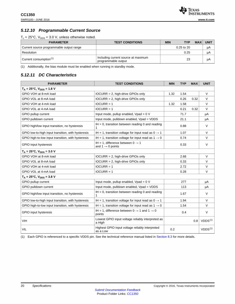
5.12.10 Programmable Current Source
(1) Additionally, the bias module must be enabled when running in standby mode.
Tc = 25°C, VDDS = 3.0 V, unless otherwise noted.PARAMETER TEST CONDITIONS MIN TYP MAX UNIT
Current source programmable output range 0.25 to 20 µAResolution 0.25 µA
Current consumption (1) Including current source at maximumprogrammable output 23 µA
5.12.11 DC Characteristics
(1) Each GPIO is referenced to a specific VDDS pin. See the technical reference manual listed in Section 8.3 for more details.
PARAMETER TEST CONDITIONS MIN TYP MAX UNITTA = 25°C, VDDS = 1.8 VGPIO VOH at 8-mA load IOCURR = 2, high-drive GPIOs only 1.32 1.54 VGPIO VOL at 8-mA load IOCURR = 2, high-drive GPIOs only 0.26 0.32 VGPIO VOH at 4-mA load IOCURR = 1 1.32 1.58 VGPIO VOL at 4-mA load IOCURR = 1 0.21 0.32 VGPIO pullup current Input mode, pullup enabled, Vpad = 0 V 71.7 µAGPIO pulldown current Input mode, pulldown enabled, Vpad = VDDS 21.1 µA
GPIO high/low input transition, no hysteresis IH = 0, transition between reading 0 and reading1 0.88 V
GPIO low-to-high input transition, with hysteresis IH = 1, transition voltage for input read as 0 → 1 1.07 VGPIO high-to-low input transition, with hysteresis IH = 1, transition voltage for input read as 1 → 0 0.74 V
GPIO input hysteresis IH = 1, difference between 0 → 1and 1 → 0 points 0.33 V
TA = 25°C, VDDS = 3.0 VGPIO VOH at 8-mA load IOCURR = 2, high-drive GPIOs only 2.68 VGPIO VOL at 8-mA load IOCURR = 2, high-drive GPIOs only 0.33 VGPIO VOH at 4-mA load IOCURR = 1 2.72 VGPIO VOL at 4-mA load IOCURR = 1 0.28 VTA = 25°C, VDDS = 3.8 VGPIO pullup current Input mode, pullup enabled, Vpad = 0 V 277 µAGPIO pulldown current Input mode, pulldown enabled, Vpad = VDDS 113 µA
GPIO high/low input transition, no hysteresis IH = 0, transition between reading 0 and reading1 1.67 V
GPIO low-to-high input transition, with hysteresis IH = 1, transition voltage for input read as 0 → 1 1.94 VGPIO high-to-low input transition, with hysteresis IH = 1, transition voltage for input read as 1 → 0 1.54 V
GPIO input hysteresis IH = 1, difference between 0 → 1 and 1 → 0points 0.4 V
VIH Lowest GPIO input voltage reliably interpreted asa High 0.8 VDDS (1)
VIL Highest GPIO input voltage reliably interpretedas a Low 0.2 VDDS (1)
0
SSIClk
SSIFss
SSITx
SSIRx
MSB LSB
MSB LSB
S2
S3
S1
8-bit control
4 to 16 bits output data
SSIClk
SSIFss
SSITx
SSIRxMSB LSB
S2
S3
S1
4 to 16 bits
21
CC1350www.ti.com SWRS183 –JUNE 2016
Submit Documentation FeedbackProduct Folder Links: CC1350
SpecificationsCopyright © 2016, Texas Instruments Incorporated
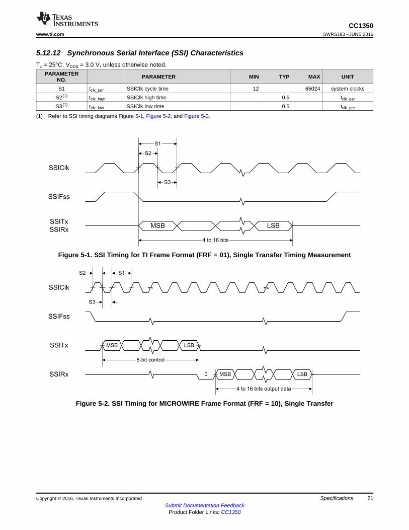
5.12.12 Synchronous Serial Interface (SSI) Characteristics
(1) Refer to SSI timing diagrams Figure 5-1, Figure 5-2, and Figure 5-3.
Tc = 25°C, VDDS = 3.0 V, unless otherwise noted.PARAMETER
NO. PARAMETER MIN TYP MAX UNIT
S1 tclk_per SSIClk cycle time 12 65024 system clocksS2 (1) tclk_high SSIClk high time 0.5 tclk_per
S3 (1) tclk_low SSIClk low time 0.5 tclk_per
Figure 5-1. SSI Timing for TI Frame Format (FRF = 01), Single Transfer Timing Measurement
Figure 5-2. SSI Timing for MICROWIRE Frame Format (FRF = 10), Single Transfer
SSIClk(SPO = 1)
SSITx(Master)
SSIRx(Slave) LSB
SSIClk(SPO = 0)
S2
S1
SSIFss
LSB
S3
MSB
MSB
22
CC1350SWRS183 –JUNE 2016 www.ti.com
Submit Documentation FeedbackProduct Folder Links: CC1350
Specifications Copyright © 2016, Texas Instruments Incorporated
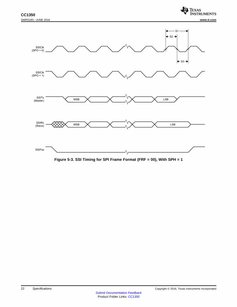
Figure 5-3. SSI Timing for SPI Frame Format (FRF = 00), With SPH = 1
VDDS (V)
AD
C C
ode
1.8 2.3 2.8 3.3 3.81004.8
1005
1005.2
1005.4
1005.6
1005.8
1006
1006.2
1006.4
D012Termperature (qC)
AD
C C
ode
-40 -20 0 20 40 60 80 1001003.5
1004
1004.5
1005
1005.5
1006
1006.5
1007
1007.5
D036
Digital Output Code
Diff
eren
tial N
onlin
earit
y (L
SB
)
0 500 1000 1500 2000 2500 3000 3500 4000-1
-0.5
0
0.5
1
1.5
D008Digital Output Code
Inte
gral
Non
linea
rity
(LS
B)
0 500 1000 1500 2000 2500 3000 3500 4000-2
-1
0
1
2
D007
VDDS (V)
Cur
rent
Con
sum
ptio
n (m
A)
1.8 2.3 2.8 3.3 3.82
2.5
3
3.5
4
4.5
5
D007
Active Mode Current
Temperature (qC)
Cur
rent
Con
sum
ptio
n (P
A)
-40 -20 0 20 40 60 80 100 1100
1
2
3
4
5
6
7
D037
23
CC1350www.ti.com SWRS183 –JUNE 2016
Submit Documentation FeedbackProduct Folder Links: CC1350
SpecificationsCopyright © 2016, Texas Instruments Incorporated
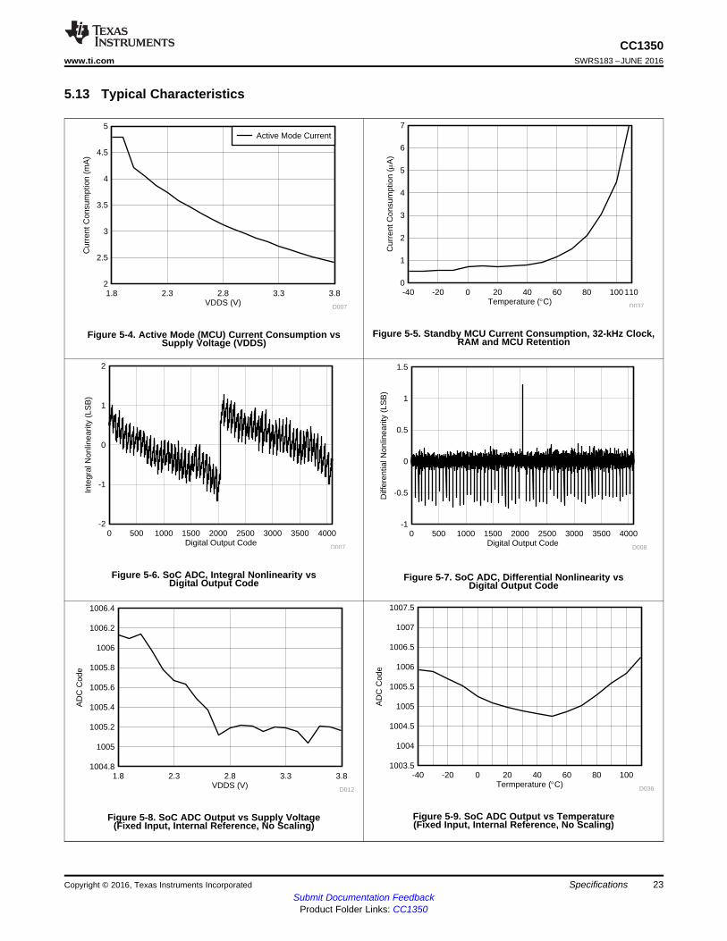
5.13 Typical Characteristics
Figure 5-4. Active Mode (MCU) Current Consumption vsSupply Voltage (VDDS)
Figure 5-5. Standby MCU Current Consumption, 32-kHz Clock,RAM and MCU Retention
Figure 5-6. SoC ADC, Integral Nonlinearity vsDigital Output Code Figure 5-7. SoC ADC, Differential Nonlinearity vs
Digital Output Code
Figure 5-8. SoC ADC Output vs Supply Voltage(Fixed Input, Internal Reference, No Scaling)
Figure 5-9. SoC ADC Output vs Temperature(Fixed Input, Internal Reference, No Scaling)

Voltage (V)
Sen
sitiv
ity (
dBm
)
1.8 2 2.2 2.4 2.6 2.8 3 3.2 3.4 3.6 3.8-111
-110.5
-110
-109.5
-109
-108.5
-108
-107.5
-107
D005Voltage (V)
Sen
sitiv
ity (
dBm
)
1.8 2 2.2 2.4 2.6 2.8 3 3.2 3.4 3.6 3.8-111
-110.5
-110
-109.5
-109
-108.5
-108
-107.5
-107
D006
Temperature (qC)
Sen
sitiv
ity (
dBm
)
-40 -20 0 20 40 60 80 100 110-112
-110
-108
-106
-104
D003Temperature (qC)
Sen
sitiv
ity (
dBm
)
-40 -20 0 20 40 60 80 100 110-112
-111
-110
-109
-108
-107
-106
D004
Frequency (MHz)
Sen
sitiv
ity (
dBm
)
863 865 867 869 871 873 875 876-112
-110
-108
-106
-104
-102
-100
D001Frequency (MHz)
Sen
sitiv
ity (
dBm
)
903 908 913 918 923 928-112
-110
-108
-106
-104
-102
-100
D002
24
CC1350SWRS183 –JUNE 2016 www.ti.com
Submit Documentation FeedbackProduct Folder Links: CC1350
Specifications Copyright © 2016, Texas Instruments Incorporated
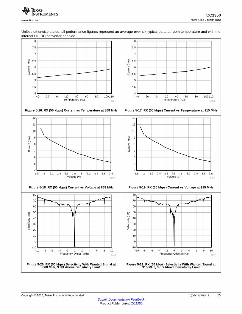
5.13.1 Typical Characteristics – Sub-1 GHzUnless otherwise stated, all performance figures represent an average over six typical parts at room temperature and with theinternal DC-DC converter enabled.
Figure 5-10. RX (50 kbps) Sensitivityvs Frequency 863 MHz to 876 MHz
Figure 5-11. RX (50 kbps) Sensitivityvs Frequency 902 MHz to 928 MHz
Figure 5-12. RX (50 kbps) Sensitivity vs Temperature 868 MHz Figure 5-13. RX (50 kbps) Sensitivity vs Temperature 915 MHz
Figure 5-14. RX (50 kbps) Sensitivity vs Voltage 868 MHz Figure 5-15. RX (50 kbps) Sensitivity vs Voltage 915 MHz
Frequency Offset (MHz)
Sel
ectiv
ity (
dB)
-10 -8 -6 -4 -2 0 2 4 6 8 10-10
0
10
20
30
40
50
60
70
80
D011Frequency Offset (MHz)
Sel
ectiv
ity (
dB)
-10 -8 -6 -4 -2 0 2 4 6 8 10-10
0
10
20
30
40
50
60
70
80
D012
Voltage (V)
Cur
rent
(m
A)
1.8 2 2.2 2.4 2.6 2.8 3 3.2 3.4 3.6 3.84
5
6
7
8
9
10
11
12
D009Voltage (V)
Cur
rent
(m
A)
1.8 2 2.2 2.4 2.6 2.8 3 3.2 3.4 3.6 3.84
5
6
7
8
9
10
11
12
D010
Temperature (qC)
Cur
rent
(m
A)
-40 -20 0 20 40 60 80 100 1104
4.5
5
5.5
6
6.5
7
7.5
8
D007Temperature (qC)
Cur
rent
(m
A)
-40 -20 0 20 40 60 80 100 1104
4.5
5
5.5
6
6.5
7
7.5
8
D008
25
CC1350www.ti.com SWRS183 –JUNE 2016
Submit Documentation FeedbackProduct Folder Links: CC1350
SpecificationsCopyright © 2016, Texas Instruments Incorporated
Unless otherwise stated, all performance figures represent an average over six typical parts at room temperature and with theinternal DC-DC converter enabled.
Figure 5-16. RX (50 kbps) Current vs Temperature at 868 MHz Figure 5-17. RX (50 kbps) Current vs Temperature at 915 MHz
Figure 5-18. RX (50 kbps) Current vs Voltage at 868 MHz Figure 5-19. RX (50 kbps) Current vs Voltage at 915 MHz
Figure 5-20. RX (50 kbps) Selectivity With Wanted Signal at868 MHz, 3 dB Above Sensitivity Limit
Figure 5-21. RX (50 kbps) Selectivity With Wanted Signal at915 MHz, 3 dB Above Sensitivity Limit
Temperature (qC)
Out
put P
ower
(dB
m)
-40 -20 0 20 40 60 80 10012
12.5
13
13.5
14
14.5
15
D017Temperature (qC)
Out
put P
ower
(dB
m)
-40 -20 0 20 40 60 80 10012
12.5
13
13.5
14
14.5
15
D018
Frequency (MHz)
Out
put P
ower
(dB
m)
863 865 867 869 871 873 875 87612
12.5
13
13.5
14
14.5
15
D015Frequency (MHz)
Out
put P
ower
(dB
m)
903 908 913 918 923 92812
12.5
13
13.5
14
14.5
15
D016
Frequency Offset (MHz)
Sel
ectiv
ity (
dB)
-10 -8 -6 -4 -2 0 2 4 6 8 10-10
0
10
20
30
40
50
60
70
80
D013Frequency Offset (MHz)
Sel
ectiv
ity (
dB)
-10 -8 -6 -4 -2 0 2 4 6 8 10-10
0
10
20
30
40
50
60
70
80
D014
26
CC1350SWRS183 –JUNE 2016 www.ti.com
Submit Documentation FeedbackProduct Folder Links: CC1350
Specifications Copyright © 2016, Texas Instruments Incorporated
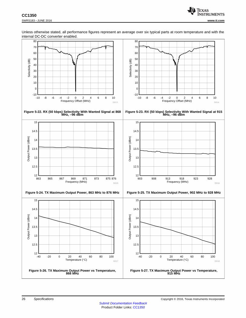
Unless otherwise stated, all performance figures represent an average over six typical parts at room temperature and with theinternal DC-DC converter enabled.
Figure 5-22. RX (50 kbps) Selectivity With Wanted Signal at 868MHz, –96 dBm
Figure 5-23. RX (50 kbps) Selectivity With Wanted Signal at 915MHz, –96 dBm
Figure 5-24. TX Maximum Output Power, 863 MHz to 876 MHz Figure 5-25. TX Maximum Output Power, 902 MHz to 928 MHz
Figure 5-26. TX Maximum Output Power vs Temperature,868 MHz
Figure 5-27. TX Maximum Output Power vs Temperature,915 MHz
Temperature (qC)
Cur
rent
(m
A)
-40 -20 0 20 40 60 80 100 11022
22.5
23
23.5
24
24.5
25
25.5
26
26.5
27
D023Temperature (qC)
Cur
rent
(m
A)
-40 -20 0 20 40 60 80 100 11022
22.5
23
23.5
24
24.5
25
25.5
26
26.5
27
D024
Frequency (MHz)
Cur
rent
(m
A)
863 865 867 869 871 873 875 87623
23.5
24
24.5
25
25.5
26
D021Frequency (MHz)
Cur
rent
(m
A)
903 908 913 918 923 92823
23.5
24
24.5
25
25.5
26
D022
Voltage (V)
Cur
rent
(m
A)
2.1 2.3 2.5 2.7 2.9 3.1 3.3 3.5 3.710
10.5
11
11.5
12
12.5
13
13.5
14
14.5
15
D019Voltage (V)
Cur
rent
(m
A)
2.1 2.3 2.5 2.7 2.9 3.1 3.3 3.5 3.710
10.5
11
11.5
12
12.5
13
13.5
14
14.5
15
D020
27
CC1350www.ti.com SWRS183 –JUNE 2016
Submit Documentation FeedbackProduct Folder Links: CC1350
SpecificationsCopyright © 2016, Texas Instruments Incorporated
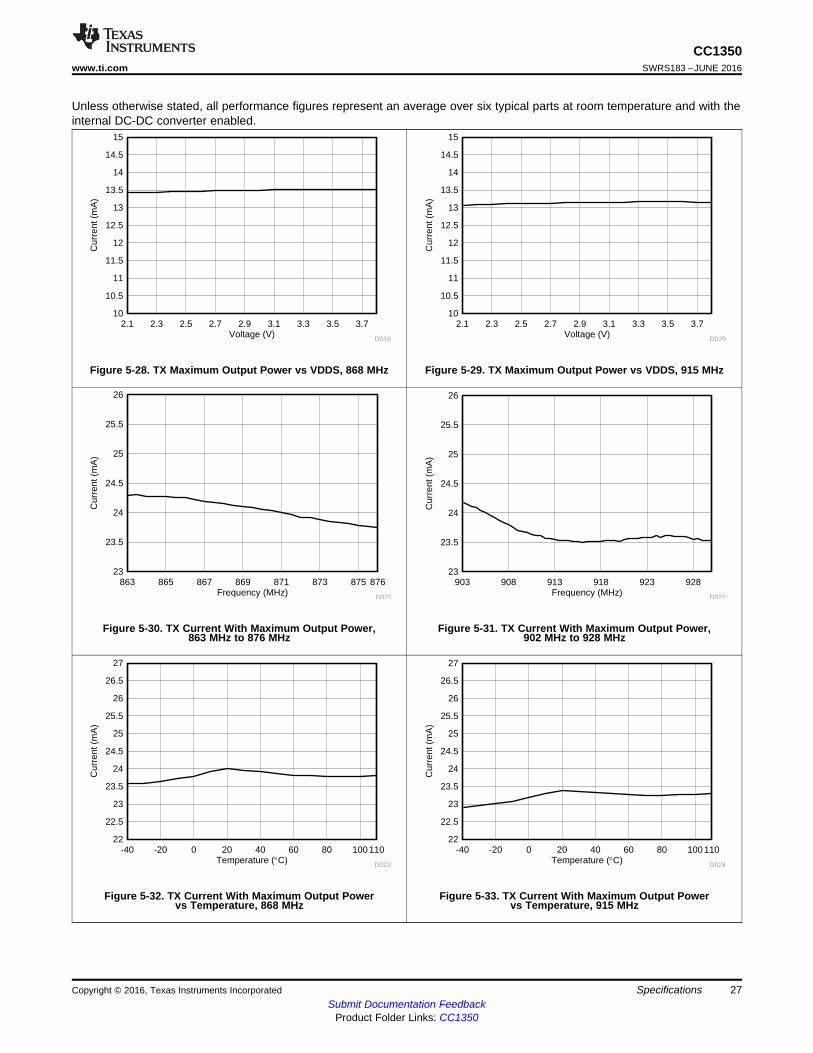
Unless otherwise stated, all performance figures represent an average over six typical parts at room temperature and with theinternal DC-DC converter enabled.
Figure 5-28. TX Maximum Output Power vs VDDS, 868 MHz Figure 5-29. TX Maximum Output Power vs VDDS, 915 MHz
Figure 5-30. TX Current With Maximum Output Power,863 MHz to 876 MHz
Figure 5-31. TX Current With Maximum Output Power,902 MHz to 928 MHz
Figure 5-32. TX Current With Maximum Output Powervs Temperature, 868 MHz
Figure 5-33. TX Current With Maximum Output Powervs Temperature, 915 MHz
Frequency (MHz)
Sen
sitiv
ity (
dBm
)
2400 2410 2420 2430 2440 2450 2460 2470 2480-90
-89
-88
-87
-86
-85
-84
-83
-82
-81
-80
D027Temperature (qC)
Cur
rent
(m
A)
-40 -20 0 20 40 60 80 100 110-90
-89
-88
-87
-86
-85
-84
-83
-82
-81
-80
D028
Voltage (V)
Cur
rent
(m
A)
2.1 2.3 2.5 2.7 2.9 3.1 3.3 3.5 3.722
24
26
28
30
32
34
36
38
40
D025Voltage (V)
Cur
rent
(m
A)
2.1 2.3 2.5 2.7 2.9 3.1 3.3 3.5 3.722
24
26
28
30
32
34
36
38
40
D026
28
CC1350SWRS183 –JUNE 2016 www.ti.com
Submit Documentation FeedbackProduct Folder Links: CC1350
Specifications Copyright © 2016, Texas Instruments Incorporated
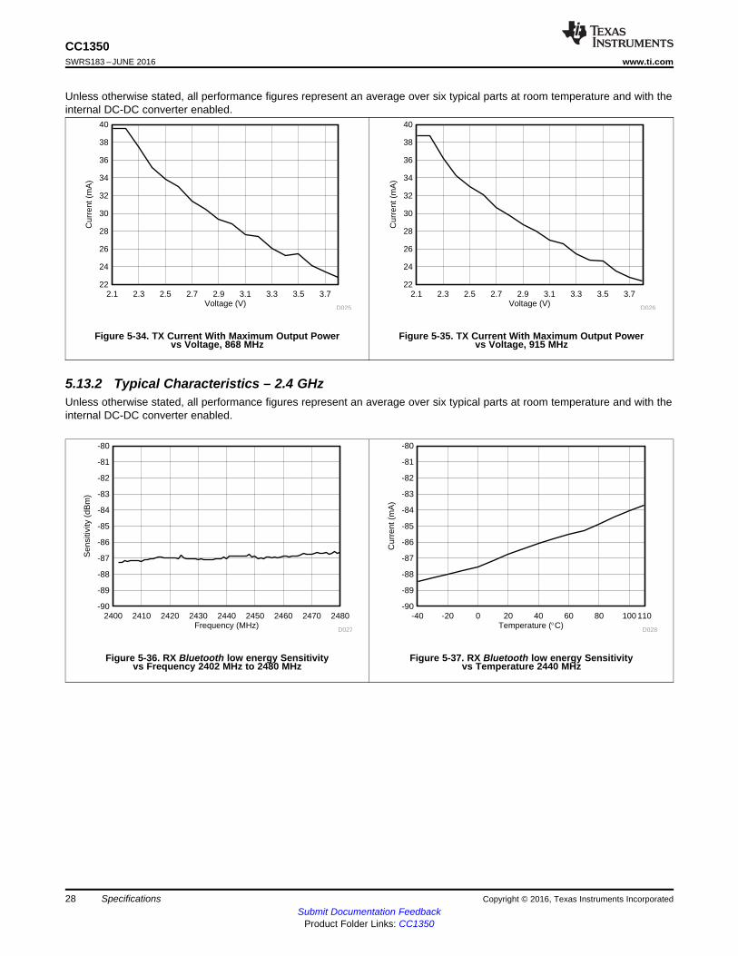
Unless otherwise stated, all performance figures represent an average over six typical parts at room temperature and with theinternal DC-DC converter enabled.
Figure 5-34. TX Current With Maximum Output Powervs Voltage, 868 MHz
Figure 5-35. TX Current With Maximum Output Powervs Voltage, 915 MHz
5.13.2 Typical Characteristics – 2.4 GHzUnless otherwise stated, all performance figures represent an average over six typical parts at room temperature and with theinternal DC-DC converter enabled.
Figure 5-36. RX Bluetooth low energy Sensitivityvs Frequency 2402 MHz to 2480 MHz
Figure 5-37. RX Bluetooth low energy Sensitivityvs Temperature 2440 MHz
Frequency (MHz)
Out
put P
ower
(dB
m)
2400 2410 2420 2430 2440 2450 2460 2470 24807
7.5
8
8.5
9
9.5
10
D033Temperature (qC)
Out
put P
ower
(dB
m)
-40 -20 0 20 40 60 80 100 1106
6.5
7
7.5
8
8.5
9
9.5
10
D034
Voltage (V)
Cur
rent
(m
A)
1.8 2 2.2 2.4 2.6 2.8 3 3.2 3.4 3.6 3.85
6
7
8
9
10
11
12
13
14
D031Frequency Offset (MHz)
Sel
ectiv
ity (
dB)
-40 -30 -20 -10 0 10 20 30 40 45-10
0
10
20
30
40
50
60
70
D032
Voltage (V)
Sen
sitiv
ity (
dBm
)
1.8 2 2.2 2.4 2.6 2.8 3 3.2 3.4 3.6 3.8-90
-89
-88
-87
-86
-85
-84
-83
-82
-81
-80
D029Temperature (qC)
Cur
rent
(m
A)
-40 -20 0 20 40 60 80 100 1105
5.5
6
6.5
7
7.5
8
D030
29
CC1350www.ti.com SWRS183 –JUNE 2016
Submit Documentation FeedbackProduct Folder Links: CC1350
SpecificationsCopyright © 2016, Texas Instruments Incorporated
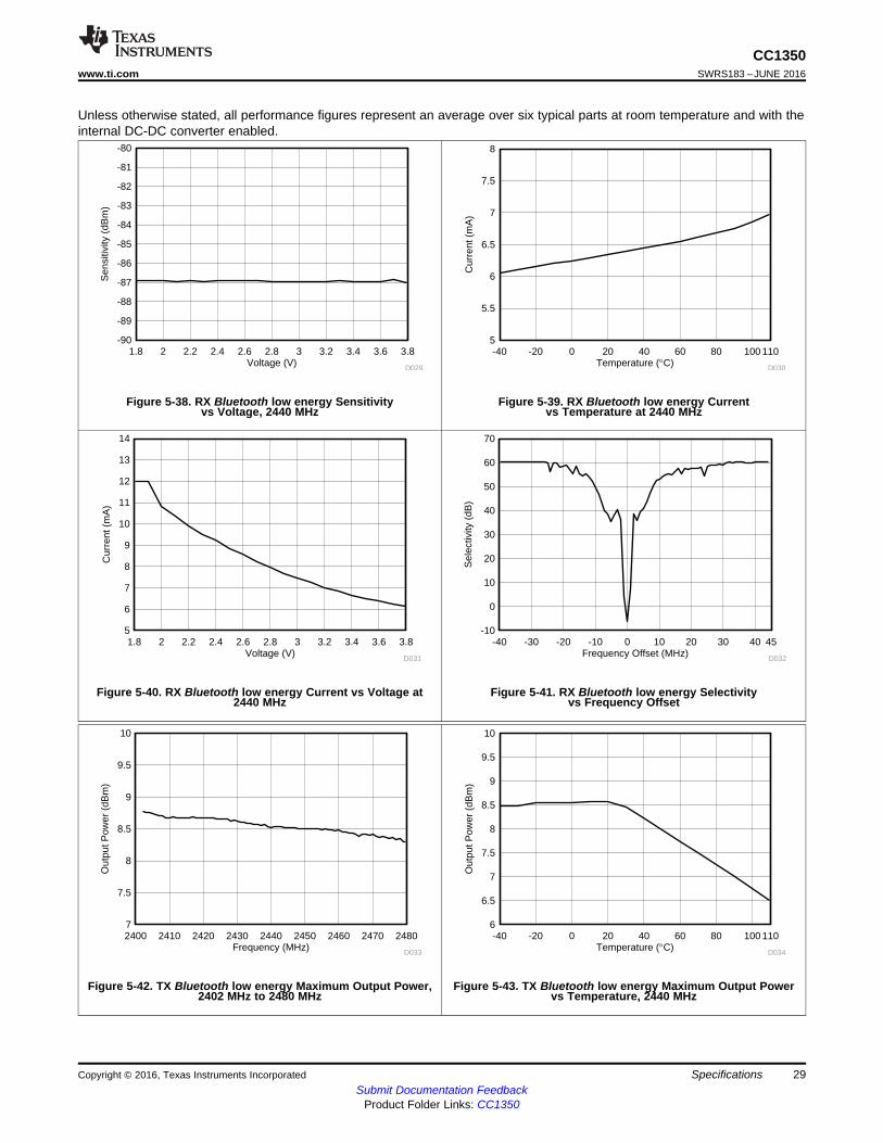
Unless otherwise stated, all performance figures represent an average over six typical parts at room temperature and with theinternal DC-DC converter enabled.
Figure 5-38. RX Bluetooth low energy Sensitivityvs Voltage, 2440 MHz
Figure 5-39. RX Bluetooth low energy Currentvs Temperature at 2440 MHz
Figure 5-40. RX Bluetooth low energy Current vs Voltage at2440 MHz
Figure 5-41. RX Bluetooth low energy Selectivityvs Frequency Offset
Figure 5-42. TX Bluetooth low energy Maximum Output Power,2402 MHz to 2480 MHz
Figure 5-43. TX Bluetooth low energy Maximum Output Powervs Temperature, 2440 MHz

Voltage (V)
Out
put P
ower
(dB
m)
2.1 2.3 2.5 2.7 2.9 3.1 3.3 3.5 3.77
7.5
8
8.5
9
9.5
10
D035
30
CC1350SWRS183 –JUNE 2016 www.ti.com
Submit Documentation FeedbackProduct Folder Links: CC1350
Specifications Copyright © 2016, Texas Instruments Incorporated
Unless otherwise stated, all performance figures represent an average over six typical parts at room temperature and with theinternal DC-DC converter enabled.
Figure 5-44. TX Bluetooth low energy Maximum Output Powervs VDDS, 2440 MHz
31
CC1350www.ti.com SWRS183 –JUNE 2016
Submit Documentation FeedbackProduct Folder Links: CC1350
Detailed DescriptionCopyright © 2016, Texas Instruments Incorporated
6 Detailed Description
6.1 OverviewFigure 1-1 shows a block diagram of the core modules of the CC13xx product family.
6.2 Main CPUThe CC1350 SimpleLink Wireless MCU contains an ARM Cortex-M3 (CM3) 32-bit CPU, which runs theapplication and the higher layers of the protocol stack.
The CM3 processor provides a high-performance, low-cost platform that meets the system requirementsof minimal memory implementation, and low-power consumption, while delivering outstandingcomputational performance and exceptional system response to interrupts.
CM3 features include the following:• 32-bit ARM Cortex-M3 architecture optimized for small-footprint embedded applications• Outstanding processing performance combined with fast interrupt handling• ARM Thumb®-2 mixed 16- and 32-bit instruction set delivers the high performance expected of a 32-bit
ARM core in a compact memory size usually associated with 8- and 16-bit devices, typically in therange of a few kilobytes of memory for microcontroller-class applications:– Single-cycle multiply instruction and hardware divide– Atomic bit manipulation (bit-banding), delivering maximum memory use and streamlined peripheral
control– Unaligned data access, enabling data to be efficiently packed into memory
• Fast code execution permits slower processor clock or increases sleep mode time• Harvard architecture characterized by separate buses for instruction and data• Efficient processor core, system, and memories• Hardware division and fast digital-signal-processing oriented multiply accumulate• Saturating arithmetic for signal processing• Deterministic, high-performance interrupt handling for time-critical applications• Enhanced system debug with extensive breakpoint and trace capabilities• Serial wire trace reduces the number of pins required for debugging and tracing• Migration from the ARM7™ processor family for better performance and power efficiency• Optimized for single-cycle flash memory use• Ultra-low power consumption with integrated sleep modes• 1.25 DMIPS per MHz

32
CC1350SWRS183 –JUNE 2016 www.ti.com
Submit Documentation FeedbackProduct Folder Links: CC1350
Detailed Description Copyright © 2016, Texas Instruments Incorporated
6.3 RF CoreThe RF core is a highly flexible and capable radio system that interfaces the analog RF and basebandcircuits, handles data to and from the system side, and assembles the information bits in a given packetstructure.
The RF core can autonomously handle the time-critical aspects of the radio protocols, thus offloading themain CPU and leaving more resources for the user application. The RF core offers a high-level,command-based API to the main CPU.
The RF core supports a wide range of modulation formats, frequency bands, and accelerator features,which include the following (not all of the features have been characterized yet, see for more information):• Wide range of data rates:
– From 625 bps (offering long range and high robustness) to as high as 4 Mbps• Wide range of modulation formats:
– Multilevel (G) FSK and MSK– On-Off Keying (OOK) with optimized shaping to minimize adjacent channel leakage– Coding-gain support for long range
• Dedicated packet handling accelerators:– Forward error correction– Data whitening– 802.15.4g mode-switch support– Automatic CRC
• Automatic listen-before-talk (LBT) and clear channel assist (CCA)• Digital RSSI• Highly configurable channel filtering, supporting channel spacing schemes from 40 kHz to 4 MHz• High degree of flexibility, offering a future-proof solution
The RF core interfaces a highly flexible radio, with a high-performance synthesizer that can support a widerange of frequency bands.
33
CC1350www.ti.com SWRS183 –JUNE 2016
Submit Documentation FeedbackProduct Folder Links: CC1350
Detailed DescriptionCopyright © 2016, Texas Instruments Incorporated
6.4 Sensor ControllerThe Sensor Controller contains circuitry that can be selectively enabled in standby mode. The peripheralsin this domain may be controlled by the Sensor Controller Engine, which is a proprietary power-optimizedCPU. This CPU can read and monitor sensors or perform other tasks autonomously; thereby significantlyreducing power consumption and offloading the main CM3 CPU.
A PC-based development tool called Sensor Controller Studio is used to write, test, and debug code forthe Sensor Controller. The tool produces C driver source code, which the System CPU application uses tocontrol and exchange data with the Sensor Controller. Typical use cases may be (but are not limited to)the following:• Analog sensors using integrated ADC• Digital sensors using GPIOs with bit-banged I2C or SPI• Capacitive sensing• Waveform generation• Pulse counting• Key scan• Quadrature decoder for polling rotational sensors
The peripherals in the Sensor Controller include the following:• The low-power clocked comparator can be used to wake the device from any state in which the
comparator is active. A configurable internal reference can be used with the comparator. The output ofthe comparator can also be used to trigger an interrupt or the ADC.
• Capacitive sensing functionality is implemented through the use of a constant current source, a time-to-digital converter, and a comparator. The continuous time comparator in this block can also be usedas a higher-accuracy alternative to the low-power clocked comparator. The Sensor Controller takescare of baseline tracking, hysteresis, filtering, and other related functions.
• The ADC is a 12-bit, 200-ksamples/s ADC with 8 inputs and a built-in voltage reference. The ADC canbe triggered by many different sources, including timers, I/O pins, software, the analog comparator,and the RTC.
• The analog modules can be connected to up to eight different GPIOs
The peripherals in the Sensor Controller can also be controlled from the main application processor.

34
CC1350SWRS183 –JUNE 2016 www.ti.com
Submit Documentation FeedbackProduct Folder Links: CC1350
Detailed Description Copyright © 2016, Texas Instruments Incorporated
(1) Up to 15 pins can be connected to the Sensor Controller. Up to eightof these pins can be connected to analog modules.
Table 6-1. GPIOs Connected to the Sensor Controller (1)
ANALOGCAPABLE
7-mm × 7-mm RGZDIO NUMBER
Y 30Y 29Y 28Y 27Y 26Y 25Y 24Y 23N 7N 6N 5N 4N 3N 2N 1
6.5 MemoryThe flash memory provides nonvolatile storage for code and data. The flash memory is in-systemprogrammable.
The SRAM (static RAM) is split into two 4-KB blocks and two 6-KB blocks and can be used to both storedata and execute code. Retention of the RAM contents in standby mode can be enabled or disabledindividually for each block to minimize power consumption. In addition, if flash cache is disabled, the 8-KBcache can be used as general-purpose RAM.
The ROM provides preprogrammed, embedded TI-RTOS kernel and Driverlib. The ROM also contains abootloader that can be used to reprogram the device using SPI or UART.
6.6 DebugThe on-chip debug support is done through a dedicated cJTAG (IEEE 1149.7) or JTAG (IEEE 1149.1)interface.
35
CC1350www.ti.com SWRS183 –JUNE 2016
Submit Documentation FeedbackProduct Folder Links: CC1350
Detailed DescriptionCopyright © 2016, Texas Instruments Incorporated
(1) Not including RTOS overhead
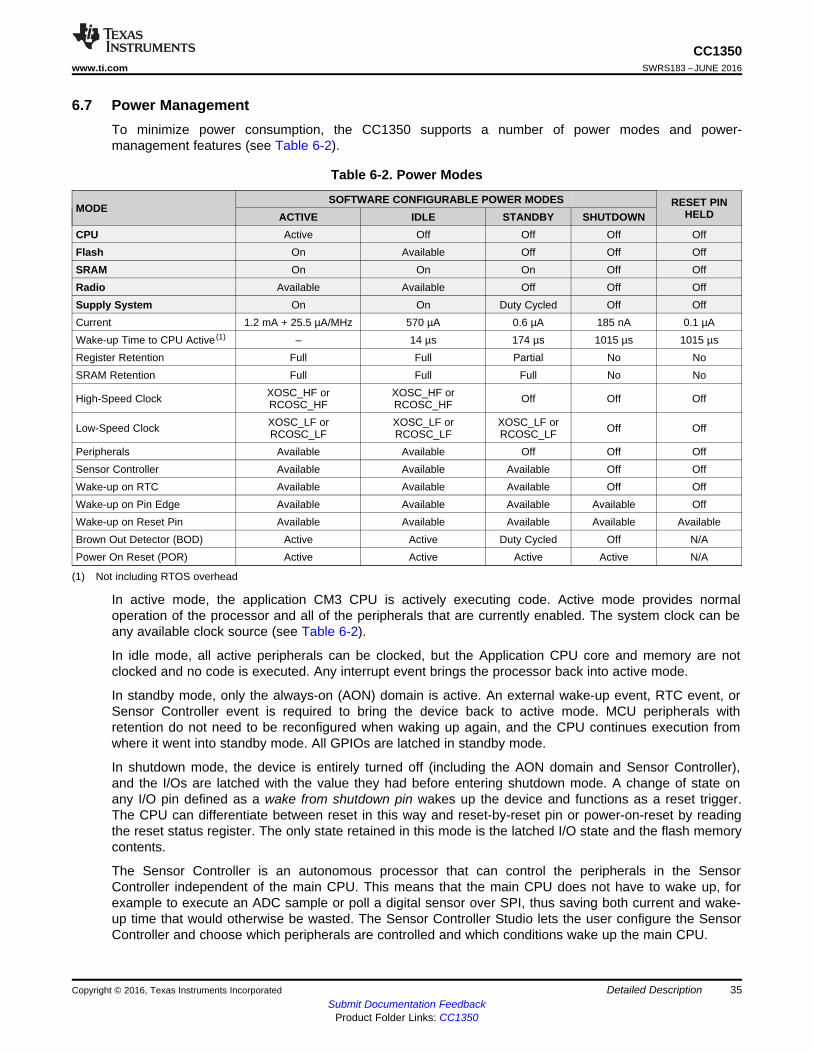
6.7 Power ManagementTo minimize power consumption, the CC1350 supports a number of power modes and power-management features (see Table 6-2).
Table 6-2. Power Modes
MODESOFTWARE CONFIGURABLE POWER MODES RESET PIN
HELDACTIVE IDLE STANDBY SHUTDOWNCPU Active Off Off Off OffFlash On Available Off Off OffSRAM On On On Off OffRadio Available Available Off Off OffSupply System On On Duty Cycled Off OffCurrent 1.2 mA + 25.5 µA/MHz 570 µA 0.6 µA 185 nA 0.1 µAWake-up Time to CPU Active (1) – 14 µs 174 µs 1015 µs 1015 µsRegister Retention Full Full Partial No NoSRAM Retention Full Full Full No No
High-Speed Clock XOSC_HF orRCOSC_HF
XOSC_HF orRCOSC_HF Off Off Off
Low-Speed Clock XOSC_LF orRCOSC_LF
XOSC_LF orRCOSC_LF
XOSC_LF orRCOSC_LF Off Off
Peripherals Available Available Off Off OffSensor Controller Available Available Available Off OffWake-up on RTC Available Available Available Off OffWake-up on Pin Edge Available Available Available Available OffWake-up on Reset Pin Available Available Available Available AvailableBrown Out Detector (BOD) Active Active Duty Cycled Off N/APower On Reset (POR) Active Active Active Active N/A
In active mode, the application CM3 CPU is actively executing code. Active mode provides normaloperation of the processor and all of the peripherals that are currently enabled. The system clock can beany available clock source (see Table 6-2).
In idle mode, all active peripherals can be clocked, but the Application CPU core and memory are notclocked and no code is executed. Any interrupt event brings the processor back into active mode.
In standby mode, only the always-on (AON) domain is active. An external wake-up event, RTC event, orSensor Controller event is required to bring the device back to active mode. MCU peripherals withretention do not need to be reconfigured when waking up again, and the CPU continues execution fromwhere it went into standby mode. All GPIOs are latched in standby mode.
In shutdown mode, the device is entirely turned off (including the AON domain and Sensor Controller),and the I/Os are latched with the value they had before entering shutdown mode. A change of state onany I/O pin defined as a wake from shutdown pin wakes up the device and functions as a reset trigger.The CPU can differentiate between reset in this way and reset-by-reset pin or power-on-reset by readingthe reset status register. The only state retained in this mode is the latched I/O state and the flash memorycontents.
The Sensor Controller is an autonomous processor that can control the peripherals in the SensorController independent of the main CPU. This means that the main CPU does not have to wake up, forexample to execute an ADC sample or poll a digital sensor over SPI, thus saving both current and wake-up time that would otherwise be wasted. The Sensor Controller Studio lets the user configure the SensorController and choose which peripherals are controlled and which conditions wake up the main CPU.

36
CC1350SWRS183 –JUNE 2016 www.ti.com
Submit Documentation FeedbackProduct Folder Links: CC1350
Detailed Description Copyright © 2016, Texas Instruments Incorporated
6.8 Clock SystemsThe CC1350 supports two external and two internal clock sources.
A 24-MHz external crystal is required as the frequency reference for the radio. This signal is doubledinternally to create a 48-MHz clock.
The 32.768-kHz crystal is optional. The low-speed crystal oscillator is designed for use with a 32.768-kHzwatch-type crystal.
The internal high-speed RC oscillator (48-MHz) can be used as a clock source for the CPU subsystem.
The internal low-speed RC oscillator (32-kHz) can be used as a reference if the low-power crystaloscillator is not used.
The 32-kHz clock source can be used as external clocking reference through GPIO.
6.9 General Peripherals and ModulesThe I/O controller controls the digital I/O pins and contains multiplexer circuitry to assign a set ofperipherals to I/O pins in a flexible manner. All digital I/Os are interrupt and wake-up capable, have aprogrammable pullup and pulldown function, and can generate an interrupt on a negative or positive edge(configurable). When configured as an output, pins can function as either push-pull or open-drain. FiveGPIOs have high-drive capabilities, which are marked in bold in Section 4, Pin Diagram—RGZ Package.
The SSIs are synchronous serial interfaces that are compatible with SPI, MICROWIRE, and TI'ssynchronous serial interfaces. The SSIs support both SPI master and slave up to 4 MHz.
The UART implements a universal asynchronous receiver and transmitter function. The UART supportsflexible baud-rate generation up to a maximum of 3 Mbps.
Timer 0 is a general-purpose timer module (GPTM) that provides two 16-bit timers. The GPTM can beconfigured to operate as a single 32-bit timer, dual 16-bit timers, or as a PWM module.
Timer 1, Timer 2, and Timer 3 are also GPTMs. Each of these timers are functionally equivalent to Timer0.
In addition to these four timers, the RF core has its own timer to handle timing for RF protocols; the RFtimer can be synchronized to the RTC.
The I2S interface is used to handle digital audio (see the CC13xx, CC26xx SimpleLink™ Wireless MCUTechnical Reference Manual for more information).
The I2C interface is used to communicate with devices compatible with the I2C standard. The I2C interfacecan handle 100 kHz and 400 kHz operation, and can serve as both I2C master and I2C slave.
The TRNG module provides a true, nondeterministic noise source for the purpose of generating keys,initialization vectors (IVs), and other random number requirements. The TRNG is built on 24 ringoscillators that create unpredictable output to feed a complex nonlinear-combinatorial circuit.
The watchdog timer is used to regain control if the system fails due to a software error after an externaldevice fails to respond as expected. The watchdog timer can generate an interrupt or a reset when apredefined time-out value is reached.
37
CC1350www.ti.com SWRS183 –JUNE 2016
Submit Documentation FeedbackProduct Folder Links: CC1350
Detailed DescriptionCopyright © 2016, Texas Instruments Incorporated
The device includes a direct memory access (µDMA) controller. The µDMA controller provides a way tooffload data-transfer tasks from the CM3 CPU, thus allowing for more efficient use of the processor andthe available bus bandwidth. The µDMA controller can perform transfer between memory and peripherals.The µDMA controller has dedicated channels for each supported on-chip module and can be programmedto automatically perform transfers between peripherals and memory when the peripheral is ready totransfer more data.
Some features of the µDMA controller include the following (this is not an exhaustive list):• Highly flexible and configurable channel operation of up to 32 channels• Transfer modes: memory-to-memory, memory-to-peripheral, peripheral-to-memory, and
peripheral-to-peripheral• Data sizes of 8, 16, and 32 bits
The AON domain contains circuitry that is always enabled, except when in shutdown mode (where thedigital supply is off). This circuitry includes the following:• The RTC can be used to wake the device from any state where it is active. The RTC contains three
compare registers and one capture register. With software support, the RTC can be used for clock andcalendar operation. The RTC is clocked from the 32-kHz RC oscillator or crystal. The RTC can also becompensated to tick at the correct frequency even when the internal 32-kHz RC oscillator is usedinstead of a crystal.
• The battery monitor and temperature sensor are accessible by software and provide a battery statusindication as well as a coarse temperature measure.
6.10 System ArchitectureDepending on the product configuration, CC1350 can function as a wireless network processor (WNP –an IC running the wireless protocol stack, with the application running on a separate host MCU), or as asystem-on-chip (SoC) with the application and protocol stack running on the ARM CM3 core inside thedevice.
In the first case, the external host MCU communicates with the device using SPI or UART. In the secondcase, the application must be written according to the application framework supplied with the wirelessprotocol stack.
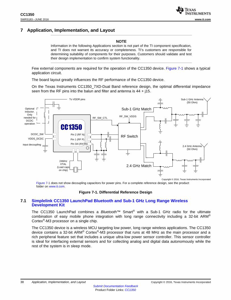
Sub-1 GHz Antenna(50 Ohm)
Pin 3/4 (RXTX)
Pin 1 (RF P)
Pin 2 (RF N)
24MHz XTAL
(Load caps on chip)
Optional inductor.
Only needed for
DCDC operation
input decoupling
To VDDR pins
VDDS_DCDC
DCDC_SW
2.4 GHz Antenna(50 Ohm)
RF Switch
Sub-1 GHz Match
2.4 GHz Match
RF_SW_CTLRF_SW_VDDS
CC 13 50
Copyright © 2016, Texas Instruments Incorporated
38
CC1350SWRS183 –JUNE 2016 www.ti.com
Submit Documentation FeedbackProduct Folder Links: CC1350
Application, Implementation, and Layout Copyright © 2016, Texas Instruments Incorporated
7 Application, Implementation, and Layout
NOTEInformation in the following Applications section is not part of the TI component specification,and TI does not warrant its accuracy or completeness. TI’s customers are responsible fordetermining suitability of components for their purposes. Customers should validate and testtheir design implementation to confirm system functionality.
Few external components are required for the operation of the CC1350 device. Figure 7-1 shows a typicalapplication circuit.
The board layout greatly influences the RF performance of the CC1350 device.
On the Texas Instruments CC1350_7XD-Dual Band reference design, the optimal differential impedanceseen from the RF pins into the balun and filter and antenna is 44 + j15.
Figure 7-1 does not show decoupling capacitors for power pins. For a complete reference design, see the productfolder on www.ti.com.
Figure 7-1. Differential Reference Design
7.1 Simplelink CC1350 LaunchPad Bluetooth and Sub-1 GHz Long Range WirelessDevelopment KitThe CC1350 LaunchPad combines a Bluetooth™ Smart® with a Sub-1 GHz radio for the ultimatecombination of easy mobile phone integration with long range connectivity including a 32-bit ARM®
Cortex®-M3 processor on a single chip.
The CC1350 device is a wireless MCU targeting low power, long range wireless applications. The CC1350device contains a 32-bit ARM® Cortex®-M3 processor that runs at 48 MHz as the main processor and arich peripheral feature set that includes a unique ultra-low power sensor controller. This sensor controlleris ideal for interfacing external sensors and for collecting analog and digital data autonomously while therest of the system is in sleep mode.
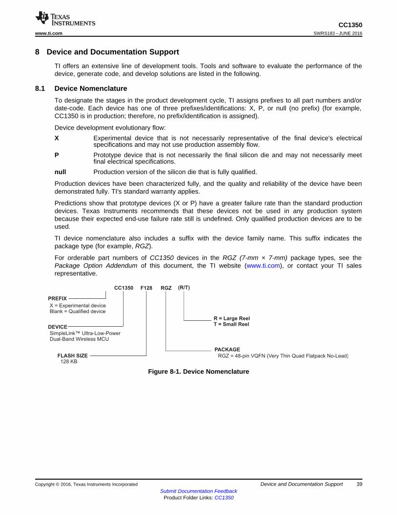
SimpleLink™ Ultra-Low-PowerDual-Band Wireless MCU
DEVICE
PREFIX
CC1350
X = Experimental deviceBlank = Qualified device
RGZ
PACKAGE
RGZ = 48-pin VQFN (Very Thin Quad Flatpack No-Lead)
(R/T)
R = Large ReelT = Small Reel
F128
FLASH SIZE128 KB
39
CC1350www.ti.com SWRS183 –JUNE 2016
Submit Documentation FeedbackProduct Folder Links: CC1350
Device and Documentation SupportCopyright © 2016, Texas Instruments Incorporated
8 Device and Documentation Support
TI offers an extensive line of development tools. Tools and software to evaluate the performance of thedevice, generate code, and develop solutions are listed in the following.
8.1 Device NomenclatureTo designate the stages in the product development cycle, TI assigns prefixes to all part numbers and/ordate-code. Each device has one of three prefixes/identifications: X, P, or null (no prefix) (for example,CC1350 is in production; therefore, no prefix/identification is assigned).
Device development evolutionary flow:X Experimental device that is not necessarily representative of the final device's electrical
specifications and may not use production assembly flow.P Prototype device that is not necessarily the final silicon die and may not necessarily meet
final electrical specifications.null Production version of the silicon die that is fully qualified.
Production devices have been characterized fully, and the quality and reliability of the device have beendemonstrated fully. TI's standard warranty applies.
Predictions show that prototype devices (X or P) have a greater failure rate than the standard productiondevices. Texas Instruments recommends that these devices not be used in any production systembecause their expected end-use failure rate still is undefined. Only qualified production devices are to beused.
TI device nomenclature also includes a suffix with the device family name. This suffix indicates thepackage type (for example, RGZ).
For orderable part numbers of CC1350 devices in the RGZ (7-mm × 7-mm) package types, see thePackage Option Addendum of this document, the TI website (www.ti.com), or contact your TI salesrepresentative.
Figure 8-1. Device Nomenclature
40
CC1350SWRS183 –JUNE 2016 www.ti.com
Submit Documentation FeedbackProduct Folder Links: CC1350
Device and Documentation Support Copyright © 2016, Texas Instruments Incorporated
8.2 Tools and SoftwareDevelopment Kit:Simplelink CC1350 LaunchPad Bluetooth and Sub-1GHz Long Range Wireless Development Kit
SPACERThe CC1350 LaunchPad combines a Bluetooth Smart with a Sub-1 GHz radio for theultimate combination of easy mobile phone integration with long range connectivity includinga 32-bit ARM Cortex-M3 processor on a single chip. The CC1350 device is a wireless MCUtargeting low power, long range wireless applications.The CC1310 device contains a 32-bit ARM Cortex-M3 processor that runs at 48 MHz as themain processor and a rich peripheral feature set that includes a unique ultra-low powersensor controller. This sensor controller is ideal for interfacing external sensors and forcollecting analog and digital data autonomously while the rest of the system is in sleepmode.
Software Tools:SmartRF Studio 7 SPACER
SmartRF Studio is a PC application that helps designers of radio systems to easily evaluatethe RF-IC at an early stage in the design process.• Test functions for transmitting and receiving radio packets, continuous wave transmit and
receive• Evaluate RF performance on custom boards by wiring it to a supported evaluation board
or debugger• Can also be used without any hardware, but then only to generate, edit and export radio
configuration settings• Can be used in combination with several development kits for Texas Instruments’
CC1350 RF-ICsSensor Controller Studio SPACER
Sensor Controller Studio provides a development environment for the CC1350 SensorController. The Sensor Controller is a proprietary, power-optimized CPU inside the CC1350 ,which can perform simple background tasks autonomously and independent of the SystemCPU state.• Allows for Sensor Controller task algorithms to be implemented using a C-like
programming language• Outputs a Sensor Controller Interface driver, which incorporates the generated Sensor
Controller machine code and associated definitions• Allows for rapid development by using the integrated Sensor Controller task testing and
debugging functionality. This allows for live visualization of sensor data and algorithmverification.
IDEs and Compilers:Code Composer Studio SPACER
• An integrated development environment with project management tools and editor• Code Composer Studio (CCS) 6.1 and later has built-in support for the CC1350 device
family• Best support for XDS debuggers; XDS100v3, XDS110 and XDS200• High integration with TI-RTOS with support for TI-RTOS Object View
IAR Embedded Workbench for ARM SPACER• Integrated development environment with project management tools and editor• IAR EWARM 7.30.3 and later has built-in support for the CC1350 device family• Broad debugger support, supporting XDS100v3, XDS200, IAR I-Jet and Segger J-Link• Integrated development environment with project management tools and editor• RTOS plugin available for TI-RTOS
For a complete listing of development-support tools for the CC1350 platform, visit the Texas Instrumentswebsite at www.ti.com. For information on pricing and availability, contact the nearest TI field sales officeor authorized distributor.
41
CC1350www.ti.com SWRS183 –JUNE 2016
Submit Documentation FeedbackProduct Folder Links: CC1350
Device and Documentation SupportCopyright © 2016, Texas Instruments Incorporated
8.3 Documentation SupportTo receive notification of documentation updates, navigate to the device product folder on ti.com(CC1350). In the upper right corner, click on Alert me to register and receive a weekly digest of anyproduct information that has changed. For change details, review the revision history included in anyrevised document.
The current documentation that describes the CC1350, related peripherals, and other technical collateralis listed in the following.
Technical Reference Manual
CC13xx, CC26xx SimpleLink™ Wireless MCU Technical Reference Manual SPACER
Reference Guide
CC26xx/CC13xx Power Management Software Developer's Reference Guide SPACER
Application ReportsUsing GCC/GDB With SimpleLink™ CC26xx/CC13xxCC-Antenna-DK2 and Antenna Measurements Summary
8.4 Texas Instruments Low-Power RF WebsiteTI's Low-Power RF website has all the latest products, application and design notes, FAQ section, newsand events updates. Go to www.ti.com/longrange.
8.5 Low-Power RF eNewsletterThe Low-Power RF eNewsletter is up-to-date on new products, news releases, developers’ news, andother news and events associated with low-power RF products from TI. The Low-Power RF eNewsletterarticles include links to get more online information.
Sign up at: www.ti.com/lprfnewsletter
8.6 Additional InformationTexas Instruments offers a wide selection of cost-effective, low-power RF solutions for proprietary andstandard-based wireless applications for use in industrial and consumer applications. The selectionincludes RF transceivers, RF transmitters, RF front ends, and Systems-on-Chips as well as varioussoftware solutions for the Sub-1 GHz and 2.4 GHz frequency bands.
In addition, Texas Instruments provides a large selection of support collateral such as development tools,technical documentation, reference designs, application expertise, customer support, third-party anduniversity programs.
Other than providing technical support forums, videos, and blogs, the Low-Power RF E2E OnlineCommunity also presents the opportunity to interact with engineers from all over the world.
With a broad selection of product solutions, end-application possibilities, and a range of technical support,Texas Instruments offers the broadest low-power RF portfolio.
42
CC1350SWRS183 –JUNE 2016 www.ti.com
Submit Documentation FeedbackProduct Folder Links: CC1350
Device and Documentation Support Copyright © 2016, Texas Instruments Incorporated
8.7 Community ResourcesThe following links connect to TI community resources. Linked contents are provided "AS IS" by therespective contributors. They do not constitute TI specifications and do not necessarily reflect TI's views;see TI's Terms of Use.TI E2E™ Online Community TI's Engineer-to-Engineer (E2E) Community. Created to foster
collaboration among engineers. At e2e.ti.com, you can ask questions, share knowledge,explore ideas and help solve problems with fellow engineers.
TI Embedded Processors Wiki Texas Instruments Embedded Processors Wiki. Established to helpdevelopers get started with Embedded Processors from Texas Instruments and to fosterinnovation and growth of general knowledge about the hardware and software surroundingthese devices.
Low-Power RF Online Community Wireless Connectivity Section of the TI E2E Support Community• Forums, videos, and blogs• RF design help• E2E interactionJoin here.
Low-Power RF Developer Network Texas Instruments has launched an extensive network of low-powerRF development partners to help customers speed up their application development. Thenetwork consists of recommended companies, RF consultants, and independent designhouses that provide a series of hardware module products and design services, including:• RF circuit, low-power RF, and ZigBee design services• Low-power RF and ZigBee module solutions and development tools• RF certification services and RF circuit manufacturingFor help with modules, engineering services or development tools:Search the Low-Power RF Developer Network to find a suitable partner.www.ti.com/lprfnetwork
8.8 TrademarksIAR Embedded Workbench is a registered trademark of IAR Systems AB.SimpleLink, SmartRF, Code Composer Studio, E2E are trademarks of Texas Instruments.ARM7 is a trademark of ARM Limited (or its subsidiaries).ARM, Cortex, Thumb are registered trademarks of ARM Limited (or its subsidiaries).Bluetooth is a registered trademark of Bluetooth SIG, Inc.ULPBench is a trademark of Embedded Microprocessor Benchmark Consortium.CoreMark is a registered trademark of Embedded Microprocessor Benchmark Consortium.IEEE Std 1241 is a trademark of Institute of Electrical and Electronics Engineers, Incorporated.Wi-SUN is a trademark of Wi-SUN Alliance, Inc.All other trademarks are the property of their respective owners.
8.9 Electrostatic Discharge CautionThis integrated circuit can be damaged by ESD. Texas Instruments recommends that all integrated circuits be handled withappropriate precautions. Failure to observe proper handling and installation procedures can cause damage.
ESD damage can range from subtle performance degradation to complete device failure. Precision integrated circuits may be moresusceptible to damage because very small parametric changes could cause the device not to meet its published specifications.
8.10 Export Control NoticeRecipient agrees to not knowingly export or re-export, directly or indirectly, any product or technical data(as defined by the U.S., EU, and other Export Administration Regulations) including software, or anycontrolled product restricted by other applicable national regulations, received from disclosing party undernondisclosure obligations (if any), or any direct product of such technology, to any destination to whichsuch export or re-export is restricted or prohibited by U.S. or other applicable laws, without obtaining priorauthorization from U.S. Department of Commerce and other competent Government authorities to theextent required by those laws.
43
CC1350www.ti.com SWRS183 –JUNE 2016
Submit Documentation FeedbackProduct Folder Links: CC1350
Mechanical Packaging and Orderable InformationCopyright © 2016, Texas Instruments Incorporated
8.11 GlossaryTI Glossary This glossary lists and explains terms, acronyms, and definitions.
9 Mechanical Packaging and Orderable Information
9.1 Packaging InformationThe following pages include mechanical packaging and orderable information. This information is the mostcurrent data available for the designated devices. This data is subject to change without notice andrevision of this document. For browser-based versions of this data sheet, refer to the left-hand navigation.
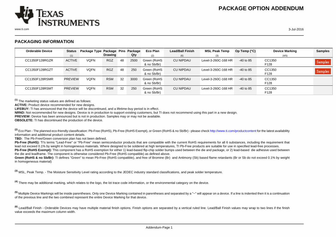
PACKAGE OPTION ADDENDUM
www.ti.com 3-Jul-2016
Addendum-Page 1
PACKAGING INFORMATION
Orderable Device Status(1)
Package Type PackageDrawing
Pins PackageQty
Eco Plan(2)
Lead/Ball Finish(6)
MSL Peak Temp(3)
Op Temp (°C) Device Marking(4/5)
Samples
CC1350F128RGZR ACTIVE VQFN RGZ 48 2500 Green (RoHS& no Sb/Br)
CU NIPDAU Level-3-260C-168 HR -40 to 85 CC1350F128
CC1350F128RGZT ACTIVE VQFN RGZ 48 250 Green (RoHS& no Sb/Br)
CU NIPDAU Level-3-260C-168 HR -40 to 85 CC1350F128
CC1350F128RSMR PREVIEW VQFN RSM 32 3000 Green (RoHS& no Sb/Br)
CU NIPDAU Level-3-260C-168 HR -40 to 85 CC1350F128
CC1350F128RSMT PREVIEW VQFN RSM 32 250 Green (RoHS& no Sb/Br)
CU NIPDAU Level-3-260C-168 HR -40 to 85 CC1350F128
(1) The marketing status values are defined as follows:ACTIVE: Product device recommended for new designs.LIFEBUY: TI has announced that the device will be discontinued, and a lifetime-buy period is in effect.NRND: Not recommended for new designs. Device is in production to support existing customers, but TI does not recommend using this part in a new design.PREVIEW: Device has been announced but is not in production. Samples may or may not be available.OBSOLETE: TI has discontinued the production of the device.
(2) Eco Plan - The planned eco-friendly classification: Pb-Free (RoHS), Pb-Free (RoHS Exempt), or Green (RoHS & no Sb/Br) - please check http://www.ti.com/productcontent for the latest availabilityinformation and additional product content details.TBD: The Pb-Free/Green conversion plan has not been defined.Pb-Free (RoHS): TI's terms "Lead-Free" or "Pb-Free" mean semiconductor products that are compatible with the current RoHS requirements for all 6 substances, including the requirement thatlead not exceed 0.1% by weight in homogeneous materials. Where designed to be soldered at high temperatures, TI Pb-Free products are suitable for use in specified lead-free processes.Pb-Free (RoHS Exempt): This component has a RoHS exemption for either 1) lead-based flip-chip solder bumps used between the die and package, or 2) lead-based die adhesive used betweenthe die and leadframe. The component is otherwise considered Pb-Free (RoHS compatible) as defined above.Green (RoHS & no Sb/Br): TI defines "Green" to mean Pb-Free (RoHS compatible), and free of Bromine (Br) and Antimony (Sb) based flame retardants (Br or Sb do not exceed 0.1% by weightin homogeneous material)
(3) MSL, Peak Temp. - The Moisture Sensitivity Level rating according to the JEDEC industry standard classifications, and peak solder temperature.
(4) There may be additional marking, which relates to the logo, the lot trace code information, or the environmental category on the device.
(5) Multiple Device Markings will be inside parentheses. Only one Device Marking contained in parentheses and separated by a "~" will appear on a device. If a line is indented then it is a continuationof the previous line and the two combined represent the entire Device Marking for that device.
(6) Lead/Ball Finish - Orderable Devices may have multiple material finish options. Finish options are separated by a vertical ruled line. Lead/Ball Finish values may wrap to two lines if the finishvalue exceeds the maximum column width.

PACKAGE OPTION ADDENDUM
www.ti.com 3-Jul-2016
Addendum-Page 2
Important Information and Disclaimer:The information provided on this page represents TI's knowledge and belief as of the date that it is provided. TI bases its knowledge and belief on informationprovided by third parties, and makes no representation or warranty as to the accuracy of such information. Efforts are underway to better integrate information from third parties. TI has taken andcontinues to take reasonable steps to provide representative and accurate information but may not have conducted destructive testing or chemical analysis on incoming materials and chemicals.TI and TI suppliers consider certain information to be proprietary, and thus CAS numbers and other limited information may not be available for release.
In no event shall TI's liability arising out of such information exceed the total purchase price of the TI part(s) at issue in this document sold by TI to Customer on an annual basis.
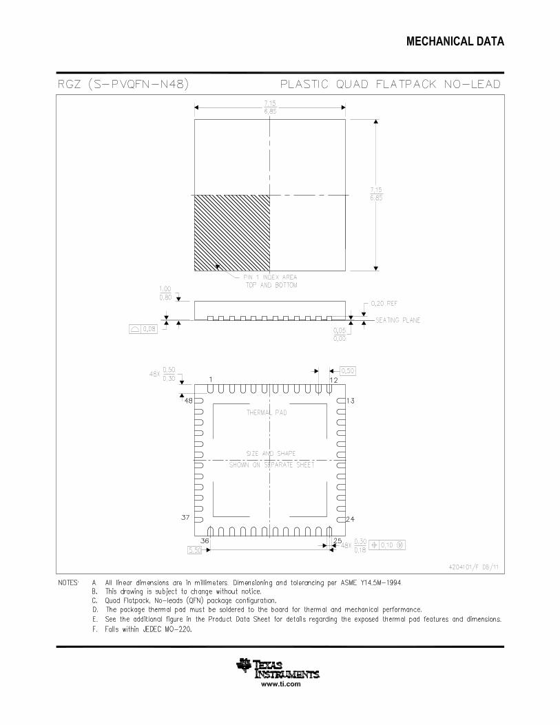
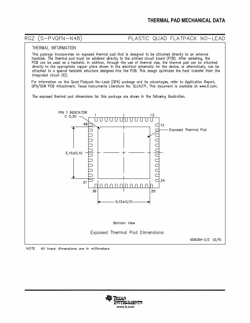
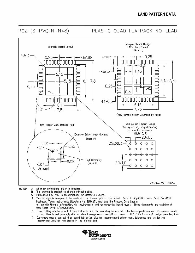
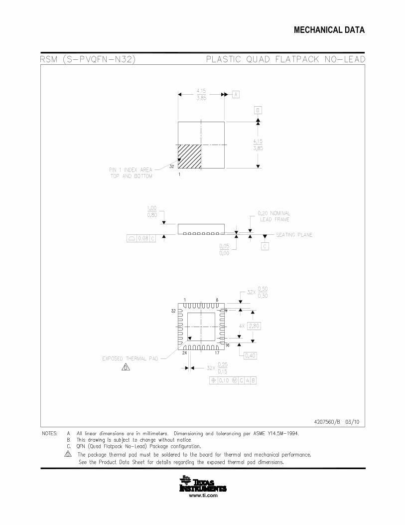
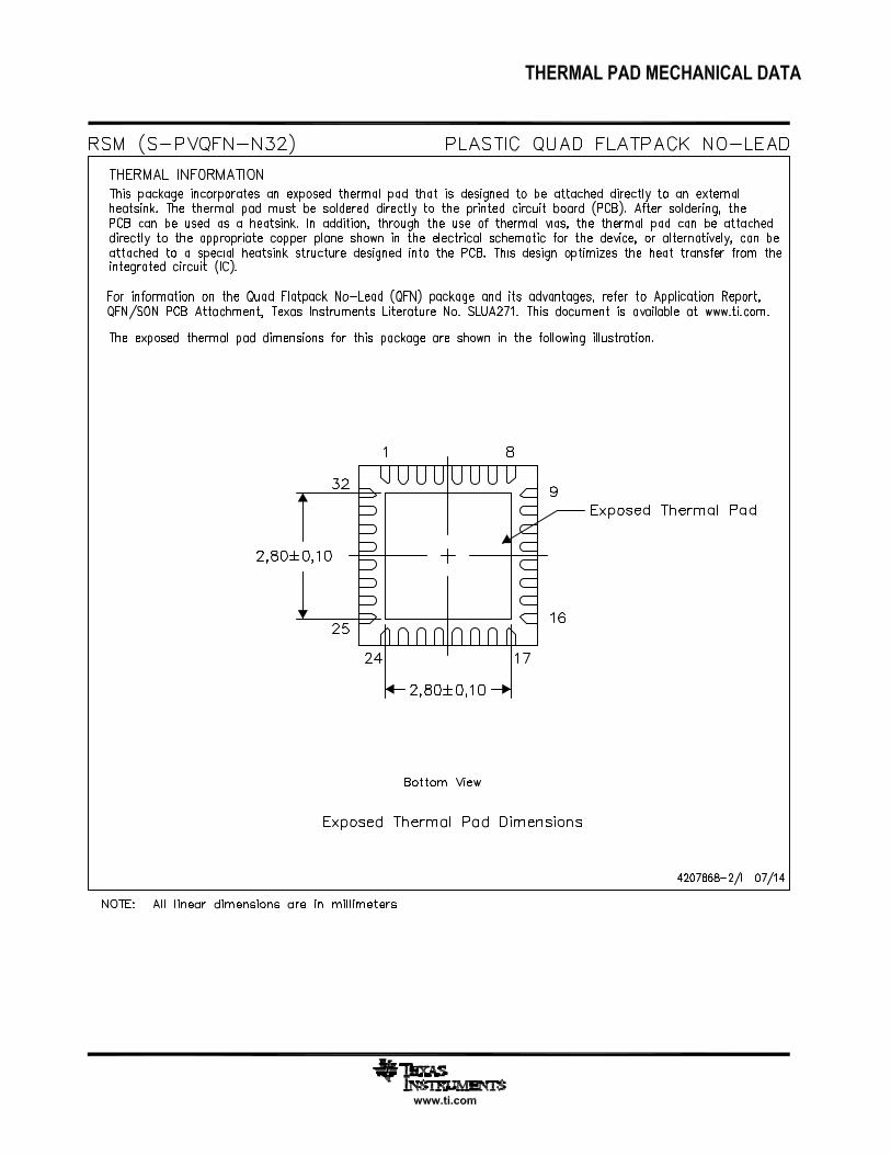
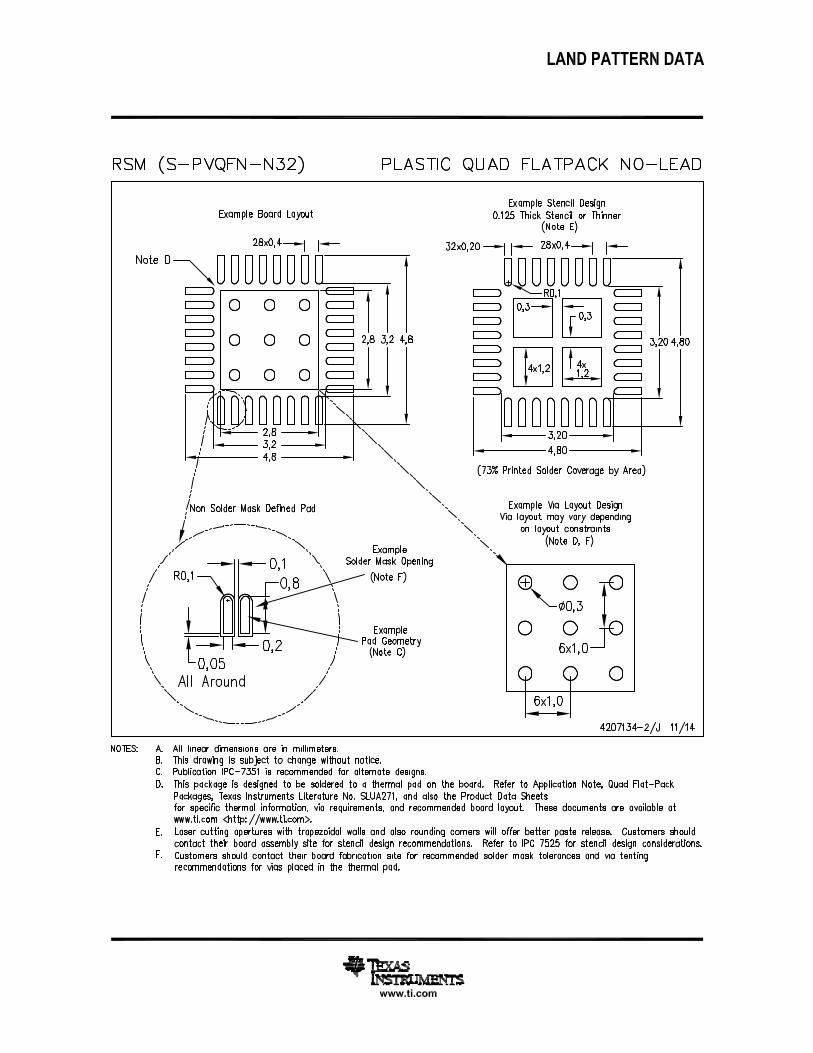
IMPORTANT NOTICE
Texas Instruments Incorporated and its subsidiaries (TI) reserve the right to make corrections, enhancements, improvements and otherchanges to its semiconductor products and services per JESD46, latest issue, and to discontinue any product or service per JESD48, latestissue. Buyers should obtain the latest relevant information before placing orders and should verify that such information is current andcomplete. All semiconductor products (also referred to herein as “components”) are sold subject to TI’s terms and conditions of salesupplied at the time of order acknowledgment.TI warrants performance of its components to the specifications applicable at the time of sale, in accordance with the warranty in TI’s termsand conditions of sale of semiconductor products. Testing and other quality control techniques are used to the extent TI deems necessaryto support this warranty. Except where mandated by applicable law, testing of all parameters of each component is not necessarilyperformed.TI assumes no liability for applications assistance or the design of Buyers’ products. Buyers are responsible for their products andapplications using TI components. To minimize the risks associated with Buyers’ products and applications, Buyers should provideadequate design and operating safeguards.TI does not warrant or represent that any license, either express or implied, is granted under any patent right, copyright, mask work right, orother intellectual property right relating to any combination, machine, or process in which TI components or services are used. Informationpublished by TI regarding third-party products or services does not constitute a license to use such products or services or a warranty orendorsement thereof. Use of such information may require a license from a third party under the patents or other intellectual property of thethird party, or a license from TI under the patents or other intellectual property of TI.Reproduction of significant portions of TI information in TI data books or data sheets is permissible only if reproduction is without alterationand is accompanied by all associated warranties, conditions, limitations, and notices. TI is not responsible or liable for such altereddocumentation. Information of third parties may be subject to additional restrictions.Resale of TI components or services with statements different from or beyond the parameters stated by TI for that component or servicevoids all express and any implied warranties for the associated TI component or service and is an unfair and deceptive business practice.TI is not responsible or liable for any such statements.Buyer acknowledges and agrees that it is solely responsible for compliance with all legal, regulatory and safety-related requirementsconcerning its products, and any use of TI components in its applications, notwithstanding any applications-related information or supportthat may be provided by TI. Buyer represents and agrees that it has all the necessary expertise to create and implement safeguards whichanticipate dangerous consequences of failures, monitor failures and their consequences, lessen the likelihood of failures that might causeharm and take appropriate remedial actions. Buyer will fully indemnify TI and its representatives against any damages arising out of the useof any TI components in safety-critical applications.In some cases, TI components may be promoted specifically to facilitate safety-related applications. With such components, TI’s goal is tohelp enable customers to design and create their own end-product solutions that meet applicable functional safety standards andrequirements. Nonetheless, such components are subject to these terms.No TI components are authorized for use in FDA Class III (or similar life-critical medical equipment) unless authorized officers of the partieshave executed a special agreement specifically governing such use.Only those TI components which TI has specifically designated as military grade or “enhanced plastic” are designed and intended for use inmilitary/aerospace applications or environments. Buyer acknowledges and agrees that any military or aerospace use of TI componentswhich have not been so designated is solely at the Buyer's risk, and that Buyer is solely responsible for compliance with all legal andregulatory requirements in connection with such use.TI has specifically designated certain components as meeting ISO/TS16949 requirements, mainly for automotive use. In any case of use ofnon-designated products, TI will not be responsible for any failure to meet ISO/TS16949.
Products ApplicationsAudio www.ti.com/audio Automotive and Transportation www.ti.com/automotiveAmplifiers amplifier.ti.com Communications and Telecom www.ti.com/communicationsData Converters dataconverter.ti.com Computers and Peripherals www.ti.com/computersDLP® Products www.dlp.com Consumer Electronics www.ti.com/consumer-appsDSP dsp.ti.com Energy and Lighting www.ti.com/energyClocks and Timers www.ti.com/clocks Industrial www.ti.com/industrialInterface interface.ti.com Medical www.ti.com/medicalLogic logic.ti.com Security www.ti.com/securityPower Mgmt power.ti.com Space, Avionics and Defense www.ti.com/space-avionics-defenseMicrocontrollers microcontroller.ti.com Video and Imaging www.ti.com/videoRFID www.ti-rfid.comOMAP Applications Processors www.ti.com/omap TI E2E Community e2e.ti.comWireless Connectivity www.ti.com/wirelessconnectivity
Mailing Address: Texas Instruments, Post Office Box 655303, Dallas, Texas 75265Copyright © 2016, Texas Instruments Incorporated