cc 110 1 m odule basic guide features - electronicos...
TRANSCRIPT

CCCCCCCC1101101101101111 MMMModuleoduleoduleodule GuideGuideGuideGuide
BasicBasicBasicBasic FFFFeatureseatureseatureseatures
1. 315,433, 868, 915Mh frequency bands of ISM and SRD2. The maximum operating speed is 500kbps, supports modulation of 2-FSK,
GFSK and MSK
3. High sensitivity (-110dDm under 1.2kbps , 1% packet error rate)4. Built-in CRC error detection and point to multipoint communication
hardware address control5. Low current consumption (RX, 15.6mA, 2.4kbps, 433MHz)
6. Programmable output power control, support up to +10 dBm for allfrequencies
7. Support low-power electromagnetic activation8. Support Clear Channel Assessment (CCA), namaly Carrier Sense Multiple

Access (CSMA).9. Support frequency hopping10. Address can be set by software, and programming is very easy11. Standard DIP interfaces12. Separate 64-byte RX and TX data FIFO
IIIInterfacenterfacenterfacenterface circuitcircuitcircuitcircuit Description:Description:Description:Description:
� VCC is connected with power supply between 1.9V~3.6V. Voltage morethan 3.6V will damage the module.Recommended voltage is 3.3V .
connected as a divider. Or it may damage the module. If the output is 3.3V,no divider is needed.
SSSStructuretructuretructuretructure andandandand pinpinpinpin descriptiondescriptiondescriptiondescription
PinNumber Pin Name Pin Type Description
1,2 VCC Power Input 1.9V~3.6V3 SI Digital Input Serial configuration interface, data input
� VCC and other pins can not be directly connected to 5V MCU IO ports, only 3.3V.
� 9 pin, 10 pin are connected to GND� Standard pitch with spacing of 2.54mm, double row
� For 51MCU, 10K pull-up resistor is necessary if connecting with P0 . Whileconnecting with other pins, it is not necessary.
� If MCU outputs 5V and more than 10mA, 2 resistors are recommended tobe
This module uses the Chipcon CC1100 chip. It is operating at433/868/915MHZ of ISM band. It consists of a frequency modulator, a receiverwith demodulator, a power amplifier, a crystal oscillator and a regulator.Preamble and the CRC code are generated automatically, wich can be easilyconfigured through SPI interface.

4 SCLK Digital Input Serial configuration interface, clock input
5 SO(GD01)
DigitalOutput
Serial configuration interface, data output.Optional general output pin when CSn ishigh
6 GDO2 DigitalOutput
Digital output pin for general use:• Test signals• FIFO status signals• Clear Channel Indicator• Clock output, down-divided from XOSC• Serial output RX data
7 CSn Digital Input Serial configuration interface, chip select
8 GDO0 Digital I/O
Digital output pin for general use:• Test signals• FIFO status signals• Clear Channel Indicator• Clock output, down-divided from XOSC• Serial output RX data• Serial input TX dataAlso used as analog test I/O forprototype/production testing
9,10 GND Ground(analog) Analog ground connection
For more configuration information, please refer to CC1101CC1101CC1101CC1101 DatasheetDatasheetDatasheetDatasheet.
ProgrammingProgrammingProgrammingProgramming GuideGuideGuideGuide
/ / CC2500/CC1100 STROBE, CONTROL AND STATUS REGSITER
# Define CCxxx0_IOCFG2 0x00 / / GDO2 output pin configuration
# Define CCxxx0_IOCFG1 0x01 / / GDO1 output pin configuration
# Define CCxxx0_IOCFG0 0x02 / / GDO0 output pin configuration
# Define CCxxx0_FIFOTHR 0x03 / / RX FIFO and TX FIFO thresholds
# Define CCxxx0_SYNC1 0x04 / / Sync word, high INT8U
# Define CCxxx0_SYNC0 0x05 / / Sync word, low INT8U
# Define CCxxx0_PKTLEN 0x06 / / Packet length
# Define CCxxx0_PKTCTRL1 0x07 / / Packet automation control

# Define CCxxx0_PKTCTRL0 0x08 / / Packet automation control
# Define CCxxx0_ADDR 0x09 / / Device address
# Define CCxxx0_CHANNR 0x0A / / Channel number
# Define CCxxx0_FSCTRL1 0x0B / / Frequency synthesizer control
# Define CCxxx0_FSCTRL0 0x0C / / Frequency synthesizer control
# Define CCxxx0_FREQ2 0x0D / / Frequency control word, high INT8U
# Define CCxxx0_FREQ1 0x0E / / Frequency control word, middle INT8U
# Define CCxxx0_FREQ0 0x0F / / Frequency control word, low INT8U
# Define CCxxx0_MDMCFG4 0x10 / / Modem configuration
# Define CCxxx0_MDMCFG3 0x11 / / Modem configuration
# Define CCxxx0_MDMCFG2 0x12 / / Modem configuration
# Define CCxxx0_MDMCFG1 0x13 / / Modem configuration
# Define CCxxx0_MDMCFG0 0x14 / / Modem configuration
# Define CCxxx0_DEVIATN 0x15 / / Modem deviation setting
# Define CCxxx0_MCSM2 0x16 / / Main Radio Control State Machine configuration
# Define CCxxx0_MCSM1 0x17 / / Main Radio Control State Machine configuration
# Define CCxxx0_MCSM0 0x18 / / Main Radio Control State Machine configuration
# Define CCxxx0_FOCCFG 0x19 / / Frequency Offset Compensation configuration
# Define CCxxx0_BSCFG 0x1A / / Bit Synchronization configuration
# Define CCxxx0_AGCCTRL2 0x1B / / AGC control
# Define CCxxx0_AGCCTRL1 0x1C / / AGC control
# Define CCxxx0_AGCCTRL0 0x1D / / AGC control
# Define CCxxx0_WOREVT1 0x1E / / High INT8U Event 0 timeout
# Define CCxxx0_WOREVT0 0x1F / / Low INT8U Event 0 timeout

# Define CCxxx0_WORCTRL 0x20 / / Wake On Radio control
# Define CCxxx0_FREND1 0x21 / / Front end RX configuration
# Define CCxxx0_FREND0 0x22 / / Front end TX configuration
# Define CCxxx0_FSCAL3 0x23 / / Frequency synthesizer calibration
# Define CCxxx0_FSCAL2 0x24 / / Frequency synthesizer calibration
# Define CCxxx0_FSCAL1 0x25 / / Frequency synthesizer calibration
# Define CCxxx0_FSCAL0 0x26 / / Frequency synthesizer calibration
# Define CCxxx0_RCCTRL1 0x27 / / RC oscillator configuration
# Define CCxxx0_RCCTRL0 0x28 / / RC oscillator configuration
# Define CCxxx0_FSTEST 0x29 / / Frequency synthesizer calibration control
# Define CCxxx0_PTEST 0x2A / / Production test
# Define CCxxx0_AGCTEST 0x2B / / AGC test
# Define CCxxx0_TEST2 0x2C / / Various test settings
# Define CCxxx0_TEST1 0x2D / / Various test settings
# Define CCxxx0_TEST0 0x2E / / Various test settings
/ / Strobe commands
# Define CCxxx0_SRES 0x30 / / Reset chip.
# Define CCxxx0_SFSTXON 0x31 / / Enable and calibrate frequency synthesizer (ifMCSM0.FS_AUTOCAL = 1).
/ / If in RX / TX: Go to a wait state where only the synthesizer is
/ / Running (for quick RX / TX turnaround).
# Define CCxxx0_SXOFF 0x32 / / Turn off crystal oscillator.
# Define CCxxx0_SCAL 0x33 / / Calibrate frequency synthesizer and turn it off
/ / (Enables quick start).
# Define CCxxx0_SRX 0x34 / / Enable RX. Perform calibration first if coming from IDLE and
/ / MCSM0.FS_AUTOCAL = 1.
# Define CCxxx0_STX 0x35 / / In IDLE state: Enable TX. Perform calibration first if
/ / MCSM0.FS_AUTOCAL = 1. If in RX state and CCA is enabled:
/ / Only go to TX if channel is clear.
# Define CCxxx0_SIDLE 0x36 / / Exit RX / TX, turn off frequency synthesizer and exit
/ / Wake-On-Radio mode if applicable.
# Define CCxxx0_SAFC 0x37 / / Perform AFC adjustment of the frequency synthesizer
# Define CCxxx0_SWOR 0x38 / / Start automatic RX polling sequence (Wake-on-Radio)
# Define CCxxx0_SPWD 0x39 / / Enter power down mode when CSn goes high.
# Define CCxxx0_SFRX 0x3A / / Flush the RX FIFO buffer.
# Define CCxxx0_SFTX 0x3B / / Flush the TX FIFO buffer.
# Define CCxxx0_SWORRST 0x3C / / Reset real time clock.
# Define CCxxx0_SNOP 0x3D / / No operation. May be used to pad strobe commands to two
/ / INT8Us for simpler software.
# Define CCxxx0_PARTNUM 0x30
# Define CCxxx0_VERSION 0x31
# Define CCxxx0_FREQEST 0x32
# Define CCxxx0_LQI 0x33
# Define CCxxx0_RSSI 0x34
# Define CCxxx0_MARCSTATE 0x35
# Define CCxxx0_WORTIME1 0x36
# Define CCxxx0_WORTIME0 0x37
# Define CCxxx0_PKTSTATUS 0x38

# Define CCxxx0_VCO_VC_DAC 0x39
# Define CCxxx0_TXBYTES 0x3A
# Define CCxxx0_RXBYTES 0x3B
# Define CCxxx0_PATABLE 0x3E
# Define CCxxx0_TXFIFO 0x3F
# Define CCxxx0_RXFIFO 0x3F
/ / RF_SETTINGS is a data structure which contains all relevant CCxxx0 registers
typedef struct S_RF_SETTINGS {
INT8U FSCTRL2; / /
INT8U FSCTRL1; / / Frequency synthesizer control.
INT8U FSCTRL0; / / Frequency synthesizer control.
INT8U FREQ2; / / Frequency control word, high INT8U.
INT8U FREQ1; / / Frequency control word, middle INT8U.
INT8U FREQ0; / / Frequency control word, low INT8U.
INT8U MDMCFG4; / / Modem configuration.
INT8U MDMCFG3; / / Modem configuration.
INT8U MDMCFG2; / / Modem configuration.
INT8U MDMCFG1; / / Modem configuration.
INT8U MDMCFG0; / / Modem configuration.
INT8U CHANNR; / / Channel number.
INT8U DEVIATN; / / Modem deviation setting (when FSK modulation is enabled).
INT8U FREND1; / / Front end RX configuration.
INT8U FREND0; / / Front end RX configuration.
INT8U MCSM0; / / Main Radio Control State Machine configuration.

INT8U FOCCFG; / / Frequency Offset Compensation Configuration.
INT8U BSCFG; / / Bit synchronization Configuration.
INT8U AGCCTRL2; / / AGC control.
INT8U AGCCTRL1; / / AGC control.
INT8U AGCCTRL0; / / AGC control.
INT8U FSCAL3; / / Frequency synthesizer calibration.
INT8U FSCAL2; / / Frequency synthesizer calibration.
INT8U FSCAL1; / / Frequency synthesizer calibration.
INT8U FSCAL0; / / Frequency synthesizer calibration.
INT8U FSTEST;
/ / Frequency synthesizer calibration control
INT8U TEST2; / / Various test settings.
INT8U TEST1; / / Various test settings.
INT8U TEST0; / / Various test settings.
INT8U IOCFG2; / / GDO2 output pin configuration
INT8U IOCFG0; / / GDO0 output pin configuration
INT8U PKTCTRL1; / / Packet automation control.
INT8U PKTCTRL0; / / Packet automation control.
INT8U ADDR; / / Device address.
INT8U PKTLEN; / / Packet length.
} RF_SETTINGS;
ConfigureConfigureConfigureConfigure thethethethe CCCCCCCC1101101101101111 modulemodulemodulemodule bybybyby readingreadingreadingreading orororor writingwritingwritingwriting totototo configurationconfigurationconfigurationconfigurationregisterregisterregisterregister throughthroughthroughthrough SPISPISPISPI interfaceinterfaceinterfaceinterface.... SPISPISPISPI serialserialserialserial interfaceinterfaceinterfaceinterface consistsconsistsconsistsconsists ofofofof fourfourfourfour lineslineslineslines::::
MOSI: Master Output Slave Input (master write)

MISO: Master Input Slave Output (master read)
SCK: Serial clock signal, controlled by master
CSN: chip select signal, low active
/ / <SPI write and read Code>
INT8U SpiTxRxByte (INT8U dat)
{
INT8U i, temp;
temp = 0;
SCK = 0;
for (i = 0; i <8; i + +)
{
if (dat & 0x80)
{
MOSI = 1;
}
else MOSI = 0;
dat <<= 1;
SCK = 1;
_nop_ ();
_nop_ ();
temp <<= 1;
if (MISO) temp + +;
SCK = 0;
_nop_ ();

_nop_ ();
}
return temp;
}
NoteNoteNoteNote :::: DataDataDataData isisisis transmitransmitransmitransmittedttedttedtted fromfromfromfrom thethethethe highhighhighhigh bitbitbitbit totototo lowlowlowlow bitbitbitbit....
/ / Configure the CC1101 module through the SPI interface, reading and writinginto configuration register>
INT8U halSpiReadReg (INT8U addr)
{
INT8U temp, value;
temp = addr | READ_SINGLE; / / read register command
CSN = 0;
while (MISO);
SpiTxRxByte (temp);
value = SpiTxRxByte (0);
CSN = 1;
return value;
}
void halSpiWriteReg (INT8U addr, INT8U value)
{
CSN = 0;
while (MISO);
SpiTxRxByte (addr); / / write address
SpiTxRxByte (value); / / write configuration

CSN = 1;
}
/ / Configure RF1100
void halRfWriteRfSettings (void)
{
halSpiWriteReg (CCxxx0_FSCTRL0, rfSettings.FSCTRL2); / / Write register settings
halSpiWriteReg (CCxxx0_FSCTRL1, rfSettings.FSCTRL1);
halSpiWriteReg (CCxxx0_FSCTRL0, rfSettings.FSCTRL0);
halSpiWriteReg (CCxxx0_FREQ2, rfSettings.FREQ2);
halSpiWriteReg (CCxxx0_FREQ1, rfSettings.FREQ1);
halSpiWriteReg (CCxxx0_FREQ0, rfSettings.FREQ0);
halSpiWriteReg (CCxxx0_MDMCFG4, rfSettings.MDMCFG4);
halSpiWriteReg (CCxxx0_MDMCFG3, rfSettings.MDMCFG3);
halSpiWriteReg (CCxxx0_MDMCFG2, rfSettings.MDMCFG2);
halSpiWriteReg (CCxxx0_MDMCFG1, rfSettings.MDMCFG1);
halSpiWriteReg (CCxxx0_MDMCFG0, rfSettings.MDMCFG0);
halSpiWriteReg (CCxxx0_CHANNR, rfSettings.CHANNR);
halSpiWriteReg (CCxxx0_DEVIATN, rfSettings.DEVIATN);
halSpiWriteReg (CCxxx0_FREND1, rfSettings.FREND1);
halSpiWriteReg (CCxxx0_FREND0, rfSettings.FREND0);
halSpiWriteReg (CCxxx0_MCSM0, rfSettings.MCSM0);
halSpiWriteReg (CCxxx0_FOCCFG, rfSettings.FOCCFG);
halSpiWriteReg (CCxxx0_BSCFG, rfSettings.BSCFG);
halSpiWriteReg (CCxxx0_AGCCTRL2, rfSettings.AGCCTRL2);
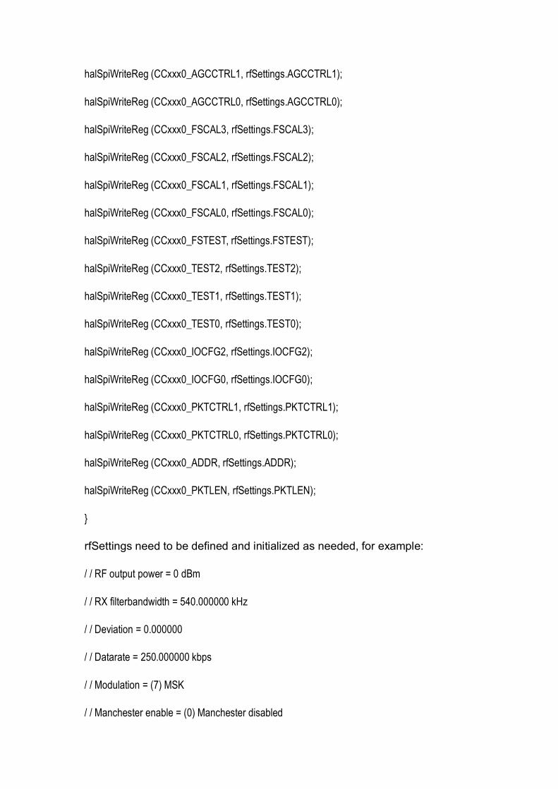
halSpiWriteReg (CCxxx0_AGCCTRL1, rfSettings.AGCCTRL1);
halSpiWriteReg (CCxxx0_AGCCTRL0, rfSettings.AGCCTRL0);
halSpiWriteReg (CCxxx0_FSCAL3, rfSettings.FSCAL3);
halSpiWriteReg (CCxxx0_FSCAL2, rfSettings.FSCAL2);
halSpiWriteReg (CCxxx0_FSCAL1, rfSettings.FSCAL1);
halSpiWriteReg (CCxxx0_FSCAL0, rfSettings.FSCAL0);
halSpiWriteReg (CCxxx0_FSTEST, rfSettings.FSTEST);
halSpiWriteReg (CCxxx0_TEST2, rfSettings.TEST2);
halSpiWriteReg (CCxxx0_TEST1, rfSettings.TEST1);
halSpiWriteReg (CCxxx0_TEST0, rfSettings.TEST0);
halSpiWriteReg (CCxxx0_IOCFG2, rfSettings.IOCFG2);
halSpiWriteReg (CCxxx0_IOCFG0, rfSettings.IOCFG0);
halSpiWriteReg (CCxxx0_PKTCTRL1, rfSettings.PKTCTRL1);
halSpiWriteReg (CCxxx0_PKTCTRL0, rfSettings.PKTCTRL0);
halSpiWriteReg (CCxxx0_ADDR, rfSettings.ADDR);
halSpiWriteReg (CCxxx0_PKTLEN, rfSettings.PKTLEN);
}
rfSettings need to be defined and initialized as needed, for example:
/ / RF output power = 0 dBm
/ / RX filterbandwidth = 540.000000 kHz
/ / Deviation = 0.000000
/ / Datarate = 250.000000 kbps
/ / Modulation = (7) MSK
/ / Manchester enable = (0) Manchester disabled

/ / RF Frequency = 433.000000 MHz
/ / Channel spacing = 199.951172 kHz
/ / Channel number = 0
/ / Optimization = Sensitivity
/ / Sync mode = (3) 30/32 sync word bits detected
/ / Format of RX / TX data = (0) Normal mode, use FIFOs for RX and TX
/ / CRC operation = (1) CRC calculation in TX and CRC check in RX enabled
/ / Forward Error Correction = (0) FEC disabled
/ / Length configuration = (1) Variable length packets, packet length configured by the firstreceived byte after sync word.
/ / Packetlength = 255
/ / Preamble count = (2) 4 bytes
/ / Append status = 1
/ / Address check = (11) No address check
/ / FIFO autoflush = 0
/ / Device address = 0
/ / GDO0 signal selection = (6)
/ / GDO2 signal selection = (11) Serial Clock
const RF_SETTINGS rfSettings = {
0x00,
0x0B, / / FSCTRL1 Frequency synthesizer control.
0x00, / / FSCTRL0 Frequency synthesizer control.
0x10, / / FREQ2 Frequency control word, high byte.
0xA7, / / FREQ1 Frequency control word, middle byte.

0x62, / / FREQ0 Frequency control word, low byte.
0x2D, / / MDMCFG4 Modem configuration.
0x3B, / / MDMCFG3 Modem configuration.
0x73, / / MDMCFG2 Modem configuration.
0x22, / / MDMCFG1 Modem configuration.
0xF8, / / MDMCFG0 Modem configuration.
0x00, / / CHANNR Channel number.
0x00, / / DEVIATN Modem deviation setting (when FSK modulation is enabled).
0xB6, / / FREND1 Front end RX configuration.
0x10, / / FREND0 Front end RX configuration.
0x18, / / MCSM0 Main Radio Control State Machine configuration.
0x1D, / / FOCCFG Frequency Offset Compensation Configuration.
0x1C, / / BSCFG Bit synchronization Configuration.
0xC7, / / AGCCTRL2 AGC control.
0x00, / / AGCCTRL1 AGC control.
0xB2, / / AGCCTRL0 AGC control.
0xEA, / / FSCAL3 Frequency synthesizer calibration.
0x0A, / / FSCAL2 Frequency synthesizer calibration.
0x00, / / FSCAL1 Frequency synthesizer calibration.
0x11, / / FSCAL0 Frequency synthesizer calibration.
0x59, / / FSTEST Frequency synthesizer calibration.
0x88, / / TEST2 Various test settings.
0x31, / / TEST1 Various test settings.
0x0B, / / TEST0 Various test settings.

0x0B, / / IOCFG2 GDO2 output pin configuration.
0x06, / / IOCFG0D GDO0 output pin configuration.
0x04, / / PKTCTRL1 Packet automation control.
0x05, / / PKTCTRL0 Packet automation control.
0x00, / / ADDR Device address.
0xff / / PKTLEN Packet length.
};
/ / Send data using the CC1100
void halRfSendPacket (INT8U * txBuffer, INT8U size)
{
halSpiWriteReg (CCxxx0_TXFIFO, size);
halSpiWriteBurstReg (CCxxx0_TXFIFO, txBuffer, size); / / write the data to be sent
halSpiStrobe (CCxxx0_STX); / / send data into the transmit mode
/ / Wait for GDO0 to be set -> sync transmitted
while (! GDO0);
/ / Wait for GDO0 to be cleared -> end of packet
while (GDO0);
halSpiStrobe (CCxxx0_SFTX);
}
/ / Receive data using the CC1100
INT8U halRfReceivePacket (INT8U * rxBuffer, INT8U * length)
{
INT8U status [2];
INT8U packetLength;

halSpiStrobe (CCxxx0_SRX); / / entry into the receiving state
while (! GDO1);
while (GDO1);
if ((halSpiReadStatus (CCxxx0_RXBYTES) & BYTES_IN_RXFIFO)) / / If the pick is not 0 bytes
{
packetLength = halSpiReadReg (CCxxx0_RXFIFO);
if (packetLength <= * length) {
halSpiReadBurstReg (CCxxx0_RXFIFO, rxBuffer, packetLength);
* Length = packetLength; / / receive data to modify the length of the length of the current data
/ / Read the 2 appended status bytes (status [0] = RSSI, status [1] = LQI)
halSpiReadBurstReg (CCxxx0_RXFIFO, status, 2); / / read CRC, bit
halSpiStrobe (CCxxx0_SFRX); / / receive buffer wash
return (status [1] & CRC_OK); / / return successfully received if the verification is successful
}
else
{
* Length = packetLength;
halSpiStrobe (CCxxx0_SFRX); / / receive buffer wash
return 0;
}
}
else
return 0;
}