cbm1307 operation instruction features general …
TRANSCRIPT

1
www.corebai.com
CBM1307
OPERATION INSTRUCTION
FEATURES
Count of seconds, minutes, hours, week
days, date, months and years with
consideration of the leap years (before
2100);
56 bytes of the power self-sufficient RAM
for the data storage;
Two-wire consecutive interface;
Programmable rectangular output signal;
Automatic determination of the supply
voltage drop and the switching diagram;
Consumption of less than 500nА in the
back-up supply mode with the operating
generator;
Temperature range of the industrial
application: -40℃ – +85℃
Accuracy is better than ±1 minute per
month
GENERAL DESCRIPTION
CBM1307 is essentially the binary –
decimal digital watch with a calendar, it has
the additional 56 bytes of the power
self-sufficient static RAM and possesses the
low power consumption. The addresses and
data are applied consecutively via the
two-wire bi-directional bus. The microcircuit
is intended for count of the real time in hours,
minutes and seconds, count of week days,
date, month and year. The last day of the
month is automatically adjusted for the
months of less, than 31 days, including
correction for the leap year. The watches
function in the 24-hour format or in the
12-hour format with the AM / PM-indicator.
CBM1307 has the built-in power supply
control circuit, which determines the supply
disruption and automatically switches over
the device into the battery mode.
PIN DISCRIPTION
Pin Symbol I/O Pin Description
1 X1 In Pin for connection of the quartz resonator
2 X2 In Pin for connection of the quartz resonator
3 VBAT In Pin for battery
4 GND In Ground pin
5 SDA Bi Input / output of serial data
6 SCL In Input of the consecutive cycle signal
7 SQW/OUT Out Output of rectangular signal
8 VCC In Power supply pin
2
www.corebai.com
CBM1307
OPERATION INSTRUCTION
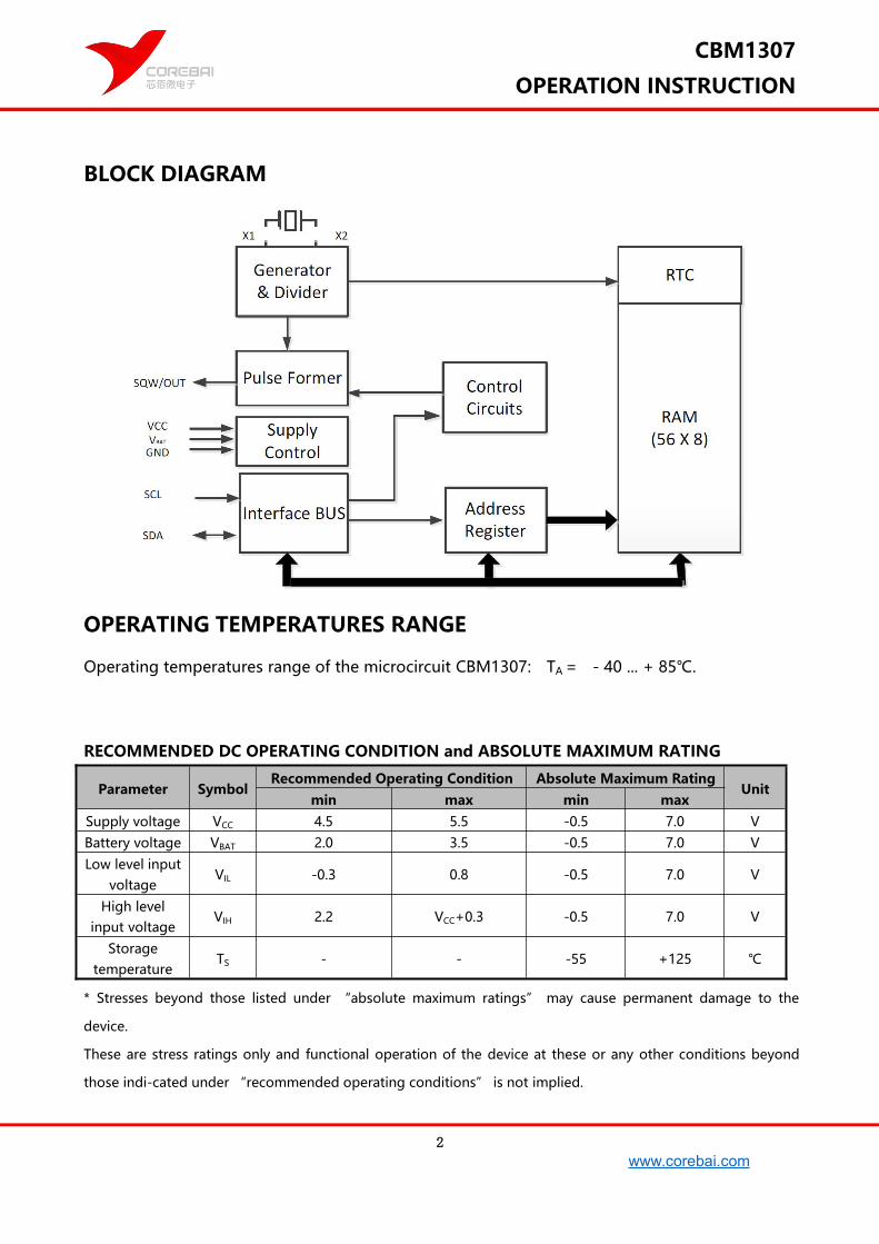
BLOCK DIAGRAM
OPERATING TEMPERATURES RANGE
Operating temperatures range of the microcircuit CBM1307: ТА = - 40 ... + 85℃.
RECOMMENDED DC OPERATING CONDITION and ABSOLUTE MAXIMUM RATING
Parameter SymbolRecommended Operating Condition Absolute Maximum Rating
Unitmin max min max
Supply voltage VСС 4.5 5.5 -0.5 7.0 VBattery voltage VBAT 2.0 3.5 -0.5 7.0 VLow level input
voltageVIL -0.3 0.8 -0.5 7.0 V
High levelinput voltage
VIH 2.2 VCC+0.3 -0.5 7.0 V
Storagetemperature
TS - - -55 +125 ℃
* Stresses beyond those listed under “absolute maximum ratings” may cause permanent damage to the
device.
These are stress ratings only and functional operation of the device at these or any other conditions beyond
those indi-cated under “recommended operating conditions” is not implied.
3
www.corebai.com
CBM1307
OPERATION INSTRUCTION
Exposure to absolute-maximum-rated conditions for extended periods may affect device reliability.
DC ELECTRICAL CHARACTERISTICS
(ТА = –40...+ 85℃, VCC = 4.5 – 5.5 V )
Parameter Symbol ModeLimit
Unitmin max
Input leakage current, (SCL only) ILI - 1 uАIn / Out leakage current,(SDA and SQW/OUT)
ILO - 1 uА
Low level output voltage VOL1) VСС = 4.5 V - 0.4 V
Consumption current in the datatransfer mode
ICCA fSCL = 100 kHz - 1500 µА
Consumption current in thestatic mode
ICCSVСС = 5 V and
SDA, SCL = 5 V- 200 µА
Consumption current in thebattery mode(SQW/OUT OFF., 32 kHz – ON)
IBAT1VCC = 0 V,VBAT = 3 V
- 0.5 µA
Consumption current in thebattery mode(SQW/OUT – ON, 32 kHz – ON)
IBAT2VCC = 0 V,VBAT = 3 V
- 0.8 µA
Low level voltage is determined under the load current of 5mА; VOL = GND under the
capacitance load
AC ELECTRICAL CHARACTERISTICS
(ТА = –40...+ 85℃, VCC = 4.5 – 5.5 V )
Parameter Symbol ModeLimit
UnitMin Max
Cycle frequency SCL fSCL - 0 100 kHz
Time of the bus vacant status between the
statuses of STOP and STARTtBUF - 4.7 - µs
Hold time (repeated) of START status tHD:STA1) - 4.0 - µs
Duration of the low status of the cycle pulse SCL tLOW - 4.7 - µs
Duration of the cycle pulse high status SCL tHIGH - 4.0 - µs
Pre-set time for the repeated status START tSU:STA - 4.7 - µs
Data hold time tHD:DAT2) - 0 - µs
Data pre-set time tSU:DAT - 250 - ns
Rise time of signals SDA and SCL tR - - 1000 ns
Drop time of signals SDA and SCL tF - - 300 ns
Pre-set time for the status STOP tSU:STO - 4.7 - ns
TotaL capacitance load per each bus line CB - - 400 pF
IN / OUT capacitance CI/O - 10 10 pF

4
www.corebai.com
CBM1307
OPERATION INSTRUCTION
Load capacitance of the quartz resonator СLX - 12.5 12.5 pF
After this time interval the first time cycle signal is formed;
Device should internally ensure the hold time, at least, 300 nsec for the signal SDA (relative to VIHMIN of signal
SCL) in order to overlap the indeterminancy area of the fall signal of SCL.
maximum value tHD:DAT should be definite in that case, if the device does not increase duration of the low
status (tLOW) of signal SCL.
TYPICAL OPERATION CHARACTERISTICS
(VCC=5.0V, TA= +25℃, unless otherwise noted)
Figure 9. Inverting Regulator Ground Referenced
Shutdown
5
www.corebai.com
CBM1307
OPERATION INSTRUCTION
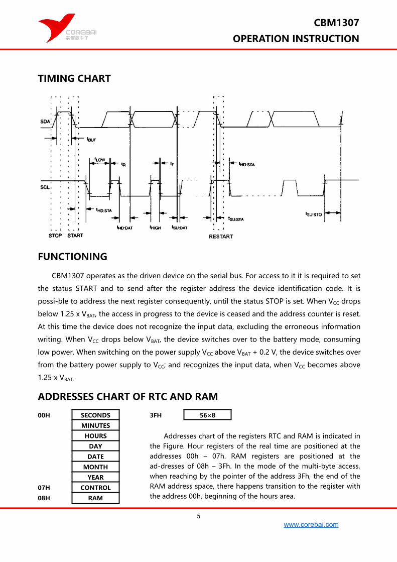
TIMING CHART
FUNCTIONING
CBM1307 operates as the driven device on the serial bus. For access to it it is required to set
the status START and to send after the register address the device identification code. It is
possi-ble to address the next register consequently, until the status STOP is set. When VCC drops
below 1.25 x VBAT, the access in progress to the device is ceased and the address counter is reset.
At this time the device does not recognize the input data, excluding the erroneous information
writing. When VCC drops below VBAT, the device switches over to the battery mode, consuming
low power. When switching on the power supply VCC above VBAT + 0.2 V, the device switches over
from the battery power supply to VCC; and recognizes the input data, when VCC becomes above
1.25 x VBAT.
ADDRESSES CHART OF RTC AND RAM
00H SECONDS
MINUTES
HOURS
DAY
DATE
MONTH
YEAR
07H CONTROL
08H RAM
3FH 56×8
Addresses chart of the registers RTC and RAM is indicated inthe Figure. Hour registers of the real time are positioned at theaddresses 00h – 07h. RAM registers are positioned at thead-dresses of 08h – 3Fh. In the mode of the multi-byte access,when reaching by the pointer of the address 3Fh, the end of theRAM address space, there happens transition to the register withthe address 00h, beginning of the hours area.
6
www.corebai.com
CBM1307
OPERATION INSTRUCTION
OSCILLATOR CIRCUIT
CBM1307 uses an external 32.768kHz crystal. The oscillator circuit does not require any
exter-nal resistors or capacitors to operate. Table specifies several crystal parameters for the
external crystal.
CRYSTAL SPECIFICATIONS*
Parameter Symbol Min Typ Max Unit
Nominal Frequency fo 32.768 kHz
Series Resistance ESR 45 kΩ
Load Capacitance CL 12.5 pF
*The crystal, traces, and crystal input pins should be isolated from RF generating signals. Application Note :
Crystal Considerations for Real-Time Clocks for additional specifications. See 12 page.
CLOCK ACCURACY
The accuracy of the clock is dependent upon the accuracy of the crystal and the accuracy of
the match between the capacitive load of the oscillator circuit and the capacitive load for which
the crystal was trimmed. Additional error will be added by crystal frequency drift caused by
tempera-ture shifts. Externalcircuit noise coupled into the oscillator.
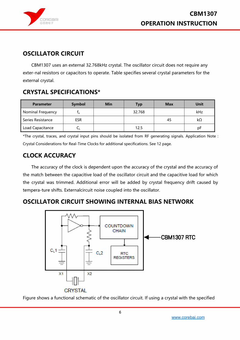
OSCILLATOR CIRCUIT SHOWING INTERNAL BIAS NETWORK
Figure shows a functional schematic of the oscillator circuit. If using a crystal with the specified

7
www.corebai.com
CBM1307
OPERATION INSTRUCTION
characteristics, the startup time is usually less than one second.
RECOMMENDED LAYOUT FOR CRYSTAL
HOURS AND CALENDAR
Information on the time and date is obtained by means of reading the appropriate register
bytes. Hour registers of the real time are indicated in the Figure. Pre-setting and time and
calendar initialization are performed by means of writing the appropriate bytes. Information,
contained in the time and calendar registers, represents the binary-decimal code. Bit 7 of register
0 represents the hour stop bit (CH). When this bit is set to “1”, the generator is off.
When switching on the power supply, the initial status of all registers is not determined. It is
necessary to enable the generator (bit CH = 0) when setting the initial configurations.
CBM1307 operates in the 12-hour or in the 24-hour format. The bit 6 of the watch register
de-termines the operational mode. 12-hour mode corresponds to the high level. In the 12-hour
mode the bit 5 is the AM/PM bit. The high level corresponds to PM. In the 24-hour mode, the 5 is
the second bit of tens of hours (20 -23 hours).
During application of the signal “START” to the two-wire bus there happens transfer of the
real time to the auxiliary set of registers. The time data are read from these auxiliary registers,
while the watch proceeds in operation. This eliminates the necessity of repeated reading in case
of updating the basic registers in the access process.

8
www.corebai.com
CBM1307
OPERATION INSTRUCTION
REGISTERS RTC CBM1307
CONTROL REGISTER
Control register is used for control of pin SQW/OUT.
BIT 7 BIT 6 BIT 5 BIT 4 BIT 3 BIT 2 BIT 1 BIT 0
OUT X X SQWE X X RS1 RS0
OUT (output control): This bit presets the output logic level of the pin SQW/OUT, when theoutput of the rectangular signal is locked.
SQWE (rectangular signal enabling): This bit, pre-set to the logic “1”, activates thegenerator output. Frequency of the output rectangular signal is determined by the bits RS0 andRS1.
RS (frequency selection): These bits determine the frequency of the output rectangularsignal, when the output of the rectangular signal is activated. The table indicates the frequencies,which can be selected by the bits RS.
RS1 RS0 Frequency SQW/OUT
0 0 1 Hz
0 1 4,096 kHz
1 0 8,192 kHz
1 1 32,768 кГц

9
www.corebai.com
CBM1307
OPERATION INSTRUCTION
TWO-WIRE SERIAL DATA BUS
CBM1307 supports the bi-directional two-wire bus and the protocol of the data exchange.The bus can be controlled by the “master” device, which generates the cycle signal (SCL),controls ac-cess to the bus, generates the statuses START and STOP. Typical configuration of thebus with the two-wire protocol is indicated in Figure.
Data transfer can be initiated only when the bus is not occupied. In the process of the datatransfer the data line should remain stable, while the line of the cycle signal is in the high status.Status alterations of the data line at that moment, when the cycle line is in the high status, will beregarded as the control signals.
In compliance with this the following conditions are determined:Bus not occupied: both the data line and the cycle signal are in the HIGH status.Data transfer start: Status alteration of the data line during transition from HIGH to LOW,
while the cycle line is in the HIGH status, is determined as the status START.Data transfer stop: Status alteration of the data line during transition from LOW to HIGH,
while the cycle line is in the HIGH status, is determined as the status STOP.Valid data: Data line status complies with the valid data, when after the status START the
data line is stable during the HIGH status of the cycle signal. Data on the line should be altered atthe time of the LOW status of the cycle signal. One cycle pulse per one data bit.
Each data transfer starts at the beginning of the status START and ceases at the beginning ofthe status STOP. Number of the data bytes, transferred between the statuses START and STOP isnot limited and is determined by the «master» device. Information is transferred byte by byte,and each receipt is confirmed by the ninth byte. CBM1307 operates in the normal mode only(100 kHz).
Confirmation of receipt: Each receiving device, when it being addressed, has to generatethe recept confirmation after receiving each byte. «Master» device should generate the cyclepulses, which are allocated in compliance with the confirmation bits.If the receipt confirmation signal is in the high status, then on arrival of the confirmation cyclepulse, the device, confirming the receipt, should switch over the SDA line to the low status. Ofcourse, there should be considered the pre-set time and the hold time. The «master» deviceshould signalize on completion of the data transfer to the “slave” device, ceasing generation ofthe confirmation bit on receiving the receipt confirmation from the “slave” cycle pulse. In thiscase, the «slave one should switch over the data line to the low status, in order to enable the«master» one generate the condition of STOP.

10
www.corebai.com
CBM1307
OPERATION INSTRUCTION
DATA TRANSFER BY THE SERIAL TWO-WIRE BUS
Depending on the status of bit ������ , there are possible two types of transfer:
1. Data are transferred from the «master» transmitter to the «slave» receiver. The first byte,
transmitted by the «master» one, is the address for the «slave» one. Then follows a sequence
of the data bytes. The «slave» one returns the receipt confirmation bytes after each received
byte. Order of the data transfer: the first is the most senior digit (MSB).
2. The data are transferred from the «slave» transmitter to the «master» receiver. The first
byte (address of «slave») is applied to the «master». Then the «master» returns the
confirmation bit. This follows after the transfer by the «slave» of the data sequence. The
«master» returns the receipt confirmation bit after each received byte, with the exception of
the last byte. After receipt of the last byte the receipt confirmation bit is not returned.
The «master» device generates all cycle pulses and the statuses START and STOP. Transfer is
completed at emergence of the status STOP or the repeated emergence of the status START. As
the repeated status START is the beginning of the next serial transfer, the bus is not vacated.The
data transfer order: the first is the most senior digit (MSB).
11
www.corebai.com
CBM1307
OPERATION INSTRUCTION
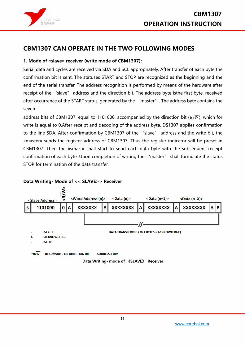
CBM1307 CAN OPERATE IN THE TWO FOLLOWING MODES
1. Mode of «slave» receiver (write mode of CBM1307):
Serial data and cycles are received via SDA and SCL appropriately. After transfer of each byte the
confirmation bit is sent. The statuses START and STOP are recognized as the beginning and the
end of the serial transfer. The address recognition is performed by means of the hardware after
receipt of the “slave” address and the direction bit. The address byte isthe first byte, received
after occurrence of the START status, generated by the “master”. The address byte contains the
seven
address bits of CBM1307, equal to 1101000, accompanied by the direction bit (������ ), which for
write is equal to 0.After receipt and decoding of the address byte, DS1307 applies confirmation
to the line SDA. After confirmation by CBM1307 of the “slave” address and the write bit, the
«master» sends the register address of CBM1307. Thus the register indicator will be preset in
CBM1307. Then the «smart» shall start to send each data byte with the subsequent receipt
confirmation of each byte. Upon completion of writing the “master” shall formulate the status
STOP for termination of the data transfer.
Data Writing- Mode of << SLAVE>> Receiver
Data Writing- mode of 《SLAVE》 Receiver

12
www.corebai.com
CBM1307
OPERATION INSTRUCTION
2. Mode of《slave》Tranceiver (read-out mode from CBM1307):
The first byte is received and processed as in the mode of the «slave» receiver. However, in
this mode the direction bit will signify, that the transmission direction is changed. CBM1307
sends the se-rial data by SDA, the cycle pulses - by SCL. statuses START and STOP are understood
as the be-ginning and end of the consecutive transmission. The address byte is the first byte,
received after occurrence of the status START, generated by the «master». The address byte
contains the seven bits of the address CBM1307, equal to 1101000, accompanied by the
direction bit (������ ), which is equal to 1 for reading. After receipt and decoding of the address
byte CBM1307 receives confirmation from the line SDA. Then CBM1307 starts to send the data
from the address, which is indicated by the register indicator. If the register indicator is not
written prior to initialization of the read mode, then the first read address is the last address ,
retained in the register indicator. CBM1307 should send the bit of «non-confirmation», in order
to complete the reading.
Data Reading – Mode of 《SLAVE》 Transmitter
Master reads after setting word address (write word address ; read data )
Data reading – mode of «slave» transmitter

13
www.corebai.com
CBM1307
OPERATION INSTRUCTION
APPLICATION NOTE
CRYSTAL CONSIDERATIONS WITH REAL-TIME CLOCKS (RTCS)
This application note describes crystal selection and layout techniques for connecting a
32,768Hz crystal to a real-time (RTC). It also provides information about oscillator circuit-design
criteria, system design, and manu-facturing issue.
OSCILLATOR BASICS
The oscillator used in RTCs is a CMOS inverter variation of a Pierce-type oscillator. Figure 1 shows
a gen-eral configuration. These RTCs include integrated load capacitors (CL1 and CL2) and bias
resistors. The Pierce oscillator utilizes a crystal operating in parallel-resonance mode. Crystals
used in parallel-resonance mode will be specified for a certal frequency with a specific load
capacitance. For the oscillator to run at the correct frequency, the oscillator circuit must load
crystal with the correct capacitive load.
Figure 1. RTC oscillator with internal load capacitors and bias resistors.
ACCURACY
The frequency accuracy of a crystal-based oscillator circuit is mainly dependent upon theaccuracy of the crystal and the accuracy of the match between the crystal and the oscillatorcapacitive load. If the capacitive load is less than the crystal was designed for, the oscillator runsfast. If the capacitive load is greater than what the crystal was designed for, the oscillator runsslow.In addition to the errors from the crystal and the load match, crystals vary from their basefrequency as the ambient temperature changes. RTCs use "tuning fork" crystals, which exhibit anerror over temperature, as shown in Figure 2 . An error of 20ppm is equivalent to approximately 1minute per month.

14
www.corebai.com
CBM1307
OPERATION INSTRUCTION
Figure 2. Crystal frequency vs. temperature.
Note: If better accuracy is required, a TCXO such as the DS32kHz can be used
CRYSTAL PARAMETERS
Figure 3 shows the equivalent circuit for a crystal. Near the resonate frequency the circuit
consists of a se-ries circuit including motional inductance L1, motional resistance R1, and
motional capacitance C1. The par-allel component C O is the shunt capacitance of the crystal.
Figure 3. Crystal equivalent circuit.
The load capacitance CL is the capacitive load of the oscillating circuit as seen from the pins ofthe crystal. Figure 4 shows CL as a capacitance in parallel with the crystal. The load capacitorsused in an oscillator circuit, CL1 and CL2, plus any stray capacitance in the circuit, combine tocreate the overall load capacitance. All RTCs have integrated CL1 and CL2 capacitors. Care shouldbe taken to minimize stray capacitance in the PC board layout. The following formula shows therelationship between CL and load capacitor values:

15
www.corebai.com
CBM1307
OPERATION INSTRUCTION
CL=[(CL1×CL2)/(CL1+CL2)+CSTRAY]
Figure 4. Crystal load capacitors and equivalent parallel load.
Most crystals allow a maximum drive level of 1μW. All RTCs run under 1μW. Drive level may be
determined using the following formula:
P=2R1×[π×32,768(CO+CL)VRMS]2,
where VRMS is the RMS value of the voltage across the crystal.
OSCILLATOR STARTUP TIME
Oscillator startup times are highly dependent upon crystal characteristics, PC board leakage, and
layout. High ESR and excessive capacitive loads are the major contributors to long startup times.
A circuit using a crystal with the recommended characteristics and proper layout usually starts
within one second.
Table 1. Crystal Specifications
Parameter Symbol Min Typ Max Units
Nominal Frequency FO 32.768 kHz
Frequency Tolerance delta F/ FO ±20 ppm
Load Capacitance CL 6 pF
Temperature Turnover Point T0 20 25 30 ℃
Parabolic Curvature Constant k 0.042 ppm/℃
Quality Factor Q 40,000 70,000
Series Resistance ESR 45 kΩ
Shunt Capacitance C0 1.1 1.8 pF
Capacitance Ratio C0/C1 430 600
Drive Level DL 1 μW
Note 1: Some devices allow higher ESR values, check the datasheet for specific requirements.
16
www.corebai.com
CBM1307
OPERATION INSTRUCTION
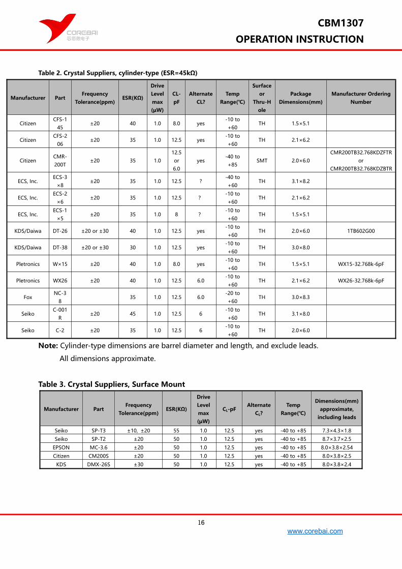
Table 2. Crystal Suppliers, cylinder-type (ESR=45kΩ)
Manufacturer PartFrequency
Tolerance(ppm)ESR(KΩ)
DriveLevelmax(μW)
CL-pF
AlternateCL?
TempRange(℃)
Surfaceor
Thru-Hole
PackageDimensions(mm)
Manufacturer OrderingNumber
CitizenCFS-1
45±20 40 1.0 8.0 yes
-10 to+60
TH 1.5×5.1
CitizenCFS-2
06±20 35 1.0 12.5 yes
-10 to+60
TH 2.1×6.2
CitizenCMR-200T
±20 35 1.012.5
or6.0
yes-40 to
+85SMT 2.0×6.0
CMR200TB32.768KDZFTRor
CMR200TB32.768KDZBTR
ECS, Inc.ECS-3
×8±20 35 1.0 12.5 ?
-40 to+60
TH 3.1×8.2
ECS, Inc.ECS-2
×6±20 35 1.0 12.5 ?
-10 to+60
TH 2.1×6.2
ECS, Inc.ECS-1
×5±20 35 1.0 8 ?
-10 to+60
TH 1.5×5.1
KDS/Daiwa DT-26 ±20 or ±30 40 1.0 12.5 yes-10 to
+60TH 2.0×6.0 1TB602G00
KDS/Daiwa DT-38 ±20 or ±30 30 1.0 12.5 yes-10 to
+60TH 3.0×8.0
Pletronics W×15 ±20 40 1.0 8.0 yes-10 to
+60TH 1.5×5.1 WX15-32.768k-6pF
Pletronics WX26 ±20 40 1.0 12.5 6.0-10 to
+60TH 2.1×6.2 WX26-32.768k-6pF
FoxNC-3
835 1.0 12.5 6.0
-20 to+60
TH 3.0×8.3
SeikoC-001
R±20 45 1.0 12.5 6
-10 to+60
TH 3.1×8.0
Seiko C-2 ±20 35 1.0 12.5 6-10 to
+60TH 2.0×6.0
Note: Cylinder-type dimensions are barrel diameter and length, and exclude leads.
All dimensions approximate.
Table 3. Crystal Suppliers, Surface Mount
Manufacturer PartFrequency
Tolerance(ppm)ESR(KΩ)
DriveLevelmax(μW)
CL-pFAlternate
CL?Temp
Range(℃)
Dimensions(mm)approximate,
including leads
Seiko SP-T3 ±10, ±20 55 1.0 12.5 yes -40 to +85 7.3×4.3×1.8
Seiko SP-T2 ±20 50 1.0 12.5 yes -40 to +85 8.7×3.7×2.5
EPSON MC-3.6 ±20 50 1.0 12.5 yes -40 to +85 8.0×3.8×2.54
Citizen CM200S ±20 50 1.0 12.5 yes -40 to +85 8.0×3.8×2.5
KDS DMX-26S ±30 50 1.0 12.5 yes -40 to +85 8.0×3.8×2.4

17
www.corebai.com
CBM1307
OPERATION INSTRUCTION
POWER CONSUMPTION
Many RTCs are designed to operate from a battery supply. In a typical application, a small
lithium bat-tery can be used to run the oscillator and clock circuitry while the main supply is off.
To maximize battery life, the oscillator must run using as little power as possible. To accomplish
this, some design tradeoffs must be made.
Negative Resistance
For typical high-frequency oscillator circuits, it is normal for the circuit to be designed with a
5 or 10X margin for the ESR. Low-frequency crystals typically have higher ESRs. An RTC oscillator
may have less than a 2X margin for negative resistance. An oscillator circuit with a low margin
normally consumes less cur-rent. As a result, an RTC oscillator often is sensitive to relatively small
amounts of stray leakage, noise, or an increase in ESR. The CL of the oscillator circuit influences
the power consumption. An RTC with 12.5pF in-ternal loads consumes more power than one that
has 6pF loads. However, the oscillator with 12.5pF load capacitors is usually less susceptible to
noise.
CRYSTAL LAYOUT GUIDELINES
Since the crystal inputs of RTCs have very high impedance (about 109 ), the leads to the
crystal act like very good antenna, coupling high-frequency signals from the rest of the system. If
a signal is coupled onto the crystal pins, it can either cancel out or add pulses. Since most of the
signals on a board are at a much higher frequency than the 32.768kHz crystal, it is more likely to
add pulses where none are wanted. These noise pulses get counted as extra clock "ticks" and
make the clock appear to run fast.
The following steps illustrate how to determine if noise is causing the RTC to run fast:
1. Power the system up and synchronize the RTC to a known accurate clock.
2. Turn the system power off.
3. Wait for a period of time (two hours, 24 hours, etc.). The longer the time period, the
easier it is to measure the accuracy of the clock.
4. Turn the system on again, read clock, and compare to the known accurate clock.
5. Resynchronize the RTC to the known accurate clock.
6. Keep the system powered up and wait for a period of time equal to the period in Step 3.
7. Read the clock after waiting for the above period of time and compare it to the known
accurate clock.

18
www.corebai.com
CBM1307
OPERATION INSTRUCTION
By using the above steps, the accuracy of the clock can be determined both when the system
is pow-ered up and when the system is powered down. If the clock proves to be inaccurate when
the system is powered up, but is accurate when the system is powered down, the problem is
most likely due to noise from other signals in the system.
However, if the clock is inaccurate both when the system is powered up and when it is
powered down, then the problem is not due to noise from the system. Since it is possible for
noise to be coupled onto the crystal pins, care must be taken when placing the external crystal
on a PC board layout. It is very important to follow a few basic layout guidelines concerning the
placement of the crystal on the PC board layout to en-sure the extra clock ticks do not couple
onto the crystal pins.
1. It is important to place the crystal as close as possible to the X1 and X2 pins. Keeping the
trace lengths between the crystal and RTC as small as possible reduces the probability of noise
coupling by reducing the length of the antenna. Keeping the trace lengths small also decreases
the amount of stray capacitance.
2. Keep the crystal bond pads and trace width to the X1 and X2 pins as small as possible.
The larger these bond pads and traces are, the more likely it is that noise can couple from
adjacent signals.
3. If possible, place a guard ring (connected to ground) around the crystal. This helps
isolate the crystal from noise coupled from adjacent signals. See Figure 2 for an illustration of
using a guard ring around a crystal.
4. Try to ensure that no signals on other PC board layers run directly below the crystal or
below the traces to the X1 and X2 pins. The more the crystal is isolated from other signals on the
board, the less likely it is that noise is coupled into the crystal. There should be a minimum of
0.200 inches be-tween any digital signal and any trace connected to X1 or X2. The RTC should be
isolated from any component that generates electromagnetic radiation (EMR). This is true for
discrete and module type RTCs.
5. It may also be helpful to place a local ground plane on the PC board layer immediately
below the crystal. This helps to isolate the crystal from noise coupling from signals on other PC
board layers. Note that the ground plane needs to be in the vicinity of the crystal only and not on
the entire board. See Figure 5 for an illustration of a local ground plane. Note that the perimeter
of the ground plane does not need to be larger than the outer perimeter of the guard ring.

19
www.corebai.com
CBM1307
OPERATION INSTRUCTION
Note that care must be taken concerning the use of a local ground plane because of the
stray capaci-tance that it introduces. The capacitance between the traces/pads and ground plane
is added to the internal load capacitors (CL1 and CL2). Therefore, some factors must be taken into
account when considering adding a local ground plane. For example, the capacitance due to the
ground plane can be approximated by the following equation:
C=εA/t, where
ε=dielectric constant of the PC board
A=area of the traces/pads
t=thickness of the PC board layer
Therefore, to determine if a ground plane is appropriate for a given design, the above
parameters must be taken into account to ensure that the capacitance from the local ground
plane is not sufficiently large enough to slow down the clock.
Figure 5. Recommended layout for crystal.
Checking For Oscillation
The first impulse that a designer has when checking for oscillator operation often is to
connect an os-cilloscope probe to the oscillator input (X1) or output (X2) pin. Doing so is not
recommended when using a Real-Time Clock. Since the oscillator is designed to run at low
power (which extends operating time from a battery), loading the oscillator with an oscilloscope
probe is likely to stop the oscillator. If the oscillator does not stop, the additional loading will
reduce the signal amplitude, and may cause erratic operation, such as varying amplitude.
Oscillation should therefore be verified indirectly.
Oscillation can be verified several ways. One method is to read the seconds register multiple
times, looking for the data to increment. On RTCs with an OSF (Oscillator Stop Flag), clearing and
then monitoring this bit will verify that the oscillator has started and is continuously running.

20
www.corebai.com
CBM1307
OPERATION INSTRUCTION
These methods won’t work if the designer is troubleshooting a design and cannot
communicate with the RTC. An alternate method is to check the square wave output on RTCs that
have a square wave output. Check the datasheet to verify if the RTC must be written first to
enable the oscillator and square wave output. Note that most RTC square wave out-puts are
open-drain, and require a pull up resistor for operation. The square wave output can also be used
to verify the accuracy of the RTC, however, a frequency counter with sufficient accuracy must be
used.
Fast Clocks
The following are the most common scenarios that cause a crystal-based RTC to run fast.
1. Noise coupling into the crystal from adjacent signals. This problem has been extensively
covered above. Noise coupling usually causes an RTC to be grossly inaccurate.
2. Wrong crystal. An RTC typically runs fast if a crystal with a specified load capacitance (CL)
greater than the RTC-specified load capacitance is used. The severity of the inaccuracy is
dependent on the value of the CL. For example, using a crystal with a CL of 12pF on an RTC
designed with a 6pF CL causes the RTC to be about 3 to 4 minutes per month fast.
Slow Clocks
The following are the most common scenarios that cause a crystal-based RTC to run slow.
1. Overshoots on RTC input pins. It is possible to cause a RTC to run slow by periodically
stopping the oscillator. This can be inadvertently accomplished by noisy input signals to the
RTC. If an input sig-nal rises to a voltage that is greater than a diode drop (~0.3V) above VDD,
the ESD protection diode for the input pin will forward bias, allowing the substrate to be
flooded with current. This, in turn, stops the oscillator until the input signal voltage
decreases to below a diode drop above VDD.
This mechanism can cause the oscillator to stop frequently if input signals are noisy.
Therefore, care should be taken to ensure there is no overshoot on input signals.
Another situation that is common to overshoot problem is having an input to the RTC at 5V
when the RTC is in battery-backup mode. This can be a problem in systems that
systematically shut down cer-tain circuits but keep others powered up. It is very important to
ensure there are no input signals to the RTC that are greater than the battery voltage (unless
stated otherwise in the device data sheet) when the device is in battery-backup mode.

21
www.corebai.com
CBM1307
OPERATION INSTRUCTION
2. Wrong crystal. A RTC typically runs slow if a crystal with a specified CL is less than the CL of
the RTC. The severity of the inaccuracy is dependent on the value of the CL.
3. Stray capacitance. Stray capacitance between the crystal pins and/or to ground can slow an
RTC down. Therefore, care must be taken when designing the PC board layout to ensure the
stray ca-pacitance is kept to a minimum.
4. Temperature. The further the operating temperature is from the crystal turnover
temperature, the slower the crystal oscillates. See Figures 3 and 4.
Clock Does Not Run
The following are the most common scenarios that cause a RTC to not run.
1. The single most common problem when the clock does not run is that the CH (clock halt) or
EOSC (enable oscillator) bit has not been set or cleared, as required. Many RTCs include a
circuit that keeps the oscillator from running when power is first applied. This allows a
system to wait for ship-ment to the customer, without drawing power from the backup
battery. When the system is powered for the first time, the software/firmware must enable
the oscillator and prompt the user for the correct time and date.
2. Surface mount crystals may have some N.C. (no connect) pins. Make sure that the correct
pins from the crystal are connected to the X1 and X2 pins.
CRYSTAL MANUFACTURING ISSUES
Tuning fork crystals should not be exposed to ultrasonic cleaning. They are susceptible to
damage from resonant vibration.
Crystals should not be exposed to temperatures above their maximum ratings. Exposure to
excessive temperatures may damage the crystal, and usually increase the ESR. Crystal "cans"
should not be soldered to a PC board. This is sometimes done to ground the case of the crystal.
Soldering directly to the case of the crystal usually subjects the unit to excessive temperatures.
RTCs should generally be used in noncondensing environments. Moisture forming around
the oscilla-tor conductors can cause leakage, which can cause the oscillator to stop. Conformal
coatings can be used to protect the circuit, however, conformal coating may by itself cause
problems.
Some conformal coatings, especially epoxy-based materials, can have unacceptable levels of
ionic contamination. In addition, conformal coatings can, if the PC board surface is not
sufficiently cleaned prior to conformal coating, cause contaminants to concentrate around leads
and traces.
Solder flux residue can cause leakage between pins. RTC oscillator circuits are especially sensitive
to leakage because of their low-power operation. Leakage between the oscillator input and
22
www.corebai.com
CBM1307
OPERATION INSTRUCTION
output, or leakage to ground, often keep the oscillator from running.
23
www.corebai.com
CBM1307
OPERATION INSTRUCTION
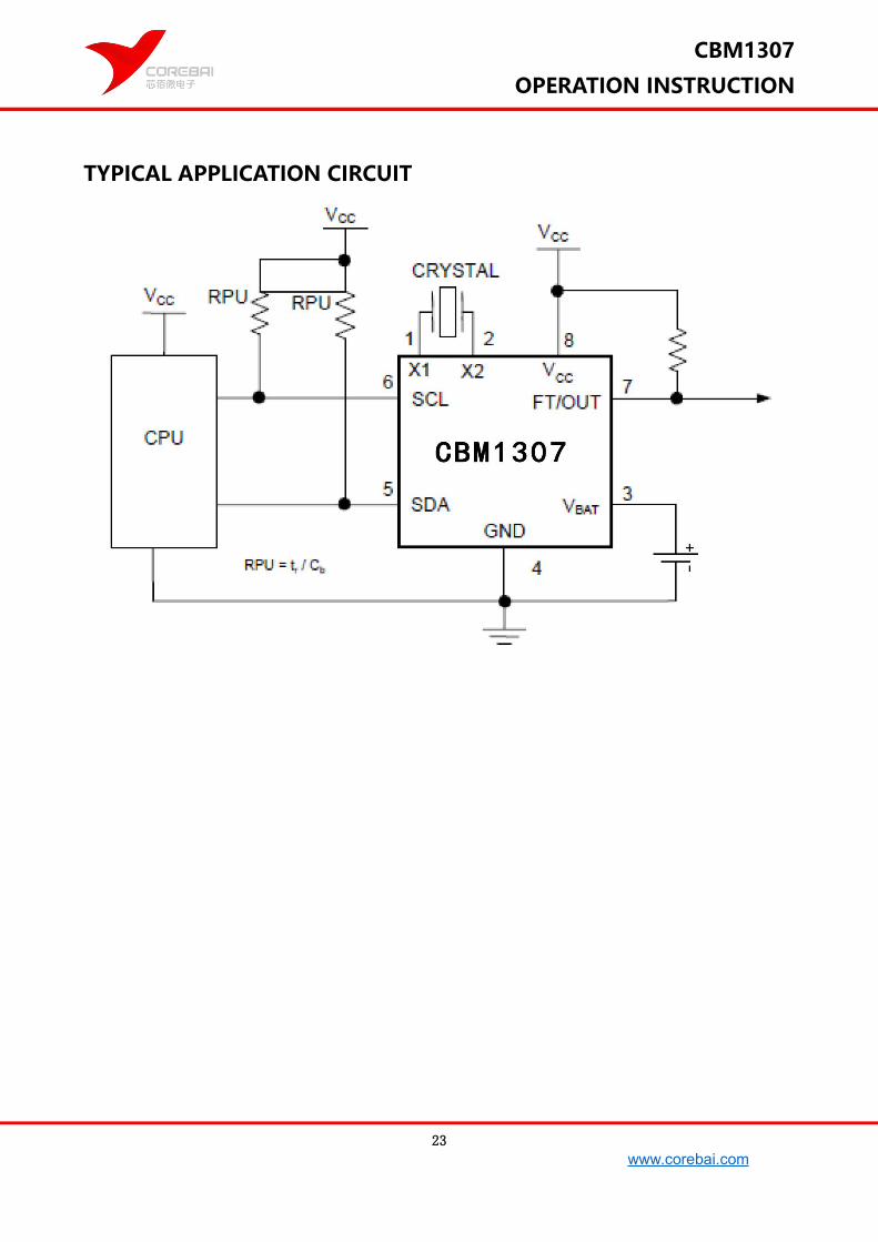
TYPICAL APPLICATION CIRCUIT
24
www.corebai.com
CBM1307
OPERATION INSTRUCTION
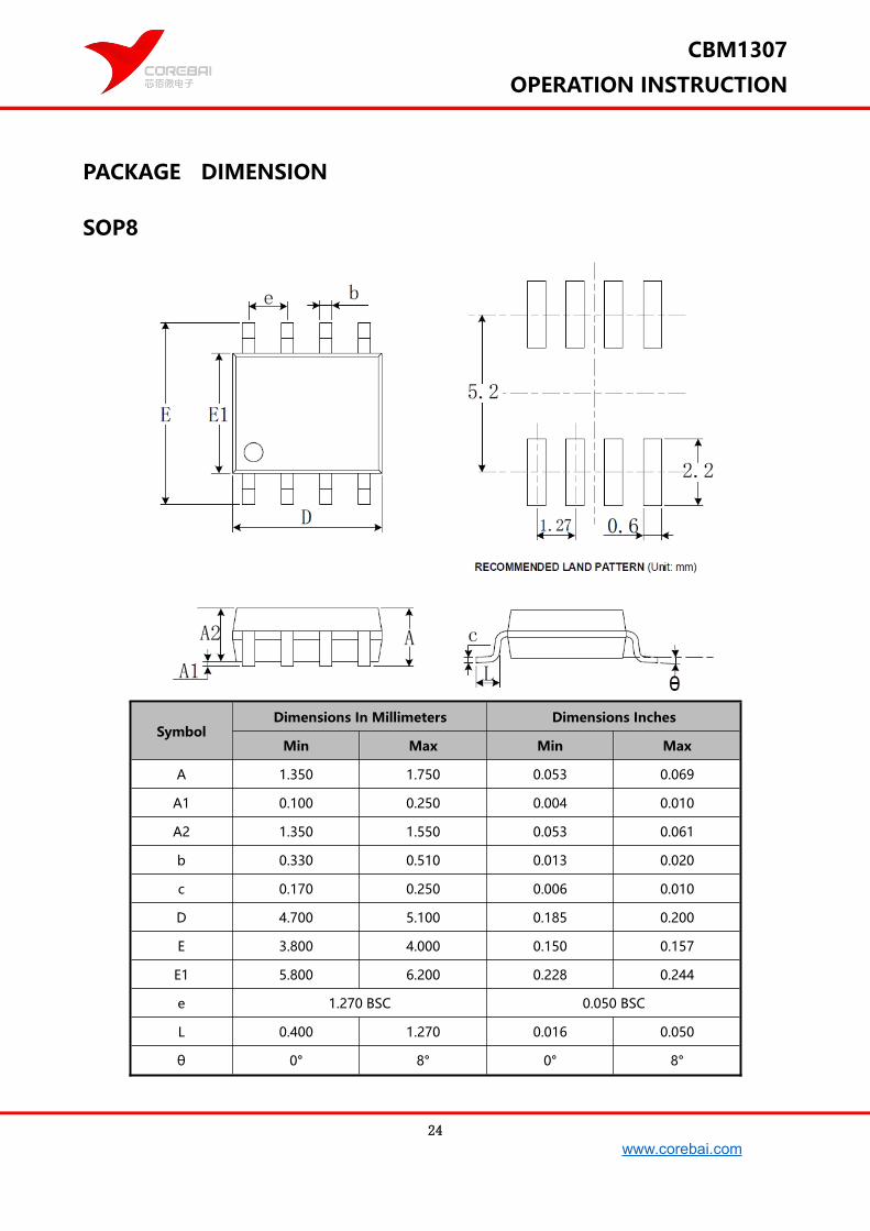
PACKAGE DIMENSION
SOP8
SymbolDimensions In Millimeters Dimensions Inches
Min Max Min Max
A 1.350 1.750 0.053 0.069
A1 0.100 0.250 0.004 0.010
A2 1.350 1.550 0.053 0.061
b 0.330 0.510 0.013 0.020
c 0.170 0.250 0.006 0.010
D 4.700 5.100 0.185 0.200
E 3.800 4.000 0.150 0.157
E1 5.800 6.200 0.228 0.244
e 1.270 BSC 0.050 BSC
L 0.400 1.270 0.016 0.050
θ 0° 8° 0° 8°

25
www.corebai.com
CBM1307
OPERATION INSTRUCTION
PACKAGE/ORDERING INFORMATION
MODELORDER
NUMBER
PACKAGE
DESCRIPTION
PACKAGE
OPTIONMARKING INFORMATION
CBM1307
CBM1307AS8 SOP-8Tape and
Reel,3000
CBM1307AD8 DIP-8Tape and
Reel,100CBM1307AD
CBM1307A
26
www.corebai.com
CBM1307
OPERATION INSTRUCTION
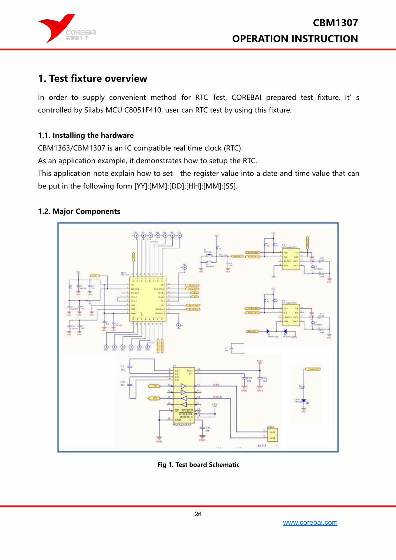
1. Test fixture overview
In order to supply convenient method for RTC Test, COREBAI prepared test fixture. It’s
controlled by Silabs MCU C8051F410, user can RTC test by using this fixture.
1.1. Installing the hardware
CBM1363/CBM1307 is an IC compatible real time clock (RTC).
As an application example, it demonstrates how to setup the RTC.
This application note explain how to set the register value into a date and time value that can
be put in the following form [YY]:[MM]:[DD]:[HH]:[MM]:[SS].
1.2. Major Components
Fig 1. Test board Schematic

27
www.corebai.com
CBM1307
OPERATION INSTRUCTION
Fig 2 Top view of test fixture
28
www.corebai.com
CBM1307
OPERATION INSTRUCTION
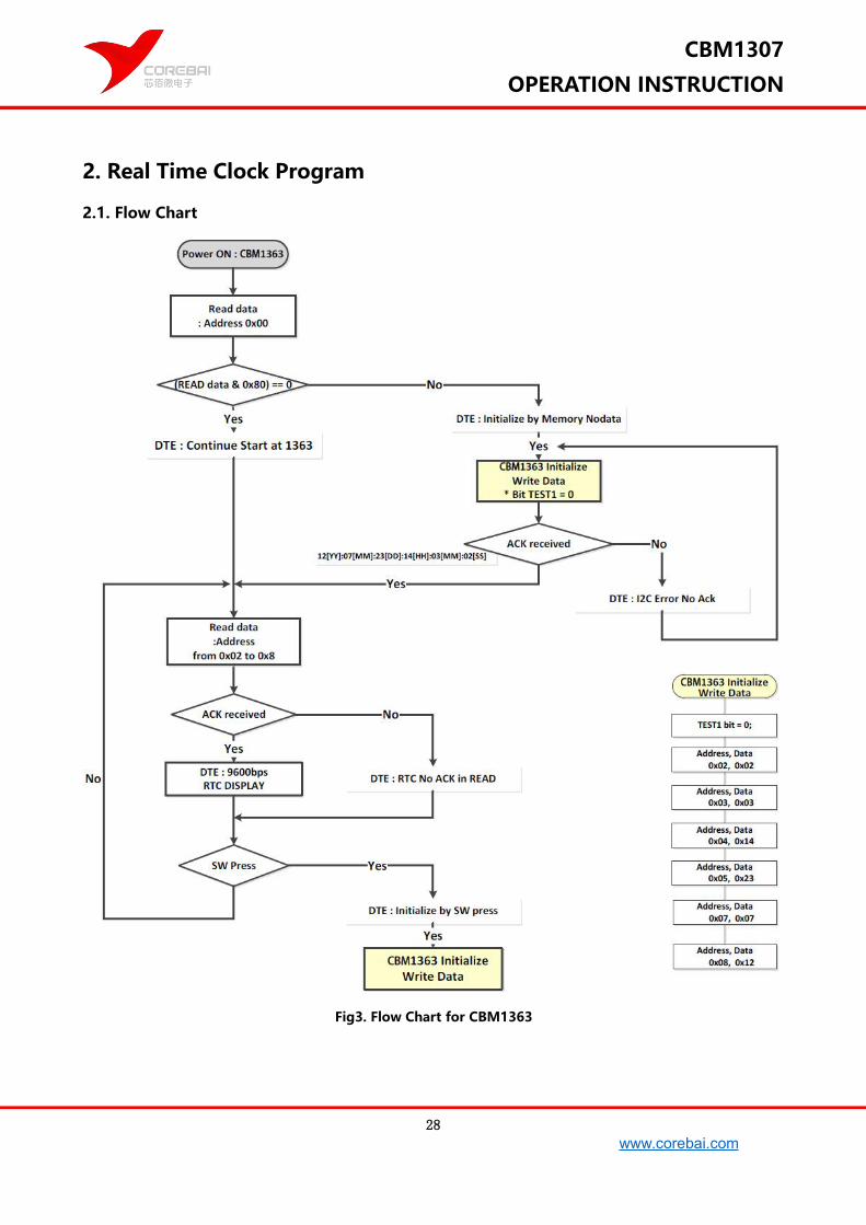
2. Real Time Clock Program
2.1. Flow Chart
Fig3. Flow Chart for CBM1363

29
www.corebai.com
CBM1307
OPERATION INSTRUCTION
Fig4. Flow Chart for CBM1307
30
www.corebai.com
CBM1307
OPERATION INSTRUCTION
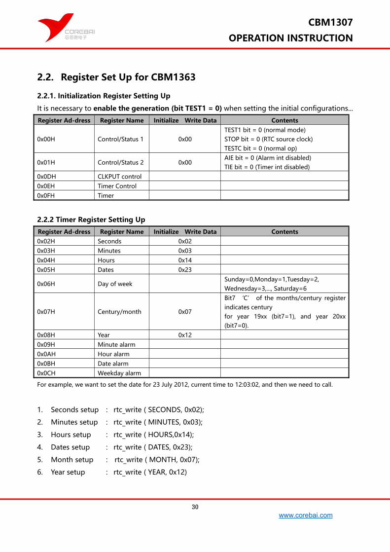
2.2. Register Set Up for CBM1363
2.2.1. Initialization Register Setting Up
It is necessary to enable the generation (bit TEST1 = 0) when setting the initial configurations...
Register Ad-dress Register Name Initialize Write Data Contents
0x00H Control/Status 1 0x00TEST1 bit = 0 (normal mode)STOP bit = 0 (RTC source clock)TESTC bit = 0 (normal op)
0x01H Control/Status 2 0x00AIE bit = 0 (Alarm int disabled)TIE bit = 0 (Timer int disabled)
0x0DH CLKPUT control0x0EH Timer Control0x0FH Timer
2.2.2 Timer Register Setting Up
Register Ad-dress Register Name Initialize Write Data Contents0x02H Seconds 0x020x03H Minutes 0x030x04H Hours 0x140x05H Dates 0x23
0x06H Day of weekSunday=0,Monday=1,Tuesday=2,Wednesday=3,..., Saturday=6
0x07H Century/month 0x07
Bit7 ‘C’ of the months/century registerindicates centuryfor year 19xx (bit7=1), and year 20xx(bit7=0).
0x08H Year 0x120x09H Minute alarm0x0AH Hour alarm0x0BH Date alarm0x0CH Weekday alarm
For example, we want to set the date for 23 July 2012, current time to 12:03:02, and then we need to call.
1. Seconds setup : rtc_write ( SECONDS, 0x02);
2. Minutes setup : rtc_write ( MINUTES, 0x03);
3. Hours setup : rtc_write ( HOURS,0x14);
4. Dates setup : rtc_write ( DATES, 0x23);
5. Month setup : rtc_write ( MONTH, 0x07);
6. Year setup : rtc_write ( YEAR, 0x12)
31
www.corebai.com
CBM1307
OPERATION INSTRUCTION
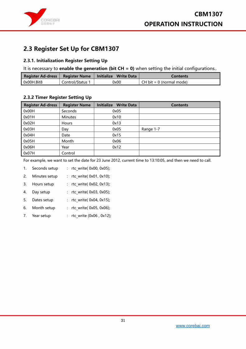
2.3 Register Set Up for CBM1307
2.3.1. Initialization Register Setting Up
It is necessary to enable the generation (bit CH = 0) when setting the initial configurations..
Register Ad-dress Register Name Initialize Write Data Contents0x00H.Bit8 Control/Status 1 0x00 CH bit = 0 (normal mode)
2.3.2 Timer Register Setting Up
Register Ad-dress Register Name Initialize Write Data Contents0x00H Seconds 0x050x01H Minutes 0x100x02H Hours 0x130x03H Day 0x05 Range 1-70x04H Date 0x150x05H Month 0x060x06H Year 0x120x07H Control
For example, we want to set the date for 23 June 2012, current time to 13:10:05, and then we need to call.
1. Seconds setup : rtc_write( 0x00, 0x05);
2. Minutes setup : rtc_write( 0x01, 0x10);
3. Hours setup : rtc_write( 0x02, 0x13);
4. Day setup : rtc_write( 0x03, 0x05);
5. Dates setup : rtc_write( 0x04, 0x15);
6. Month setup : rtc_write( 0x05, 0x06);
7. Year setup : rtc_write (0x06 , 0x12);

32
www.corebai.com
CBM1307
OPERATION INSTRUCTION
2.4 Hyper Terminal Configuration
1. Bits per second : 9600 BPS
2. Data bit : 8 bit
3. Parity bit : None
4. Stop bits : 1 bit
5. Flow Control : None
Fig5. Example test program for CBM1363
Run the Serial terminal and make sure the baud rate is set correctly at 9600bps
Fig6. CBM1363 RTC Data on Serial Terminal

33
www.corebai.com
CBM1307
OPERATION INSTRUCTION
Fig7. CBM1307 RTC Data on Serial Terminal

34
www.corebai.com
CBM1307
OPERATION INSTRUCTION
3. Example Source for RTC
This documentation shows an example of a main function to setup and read/write data. If you
request example source code, we can provide source codes.
3.1. Read Current Time from CBM1363 & CBM1307
Slave Address of CBM1363 = 0xA2
Slave Address of CBM1307 = 0xD0;
3.2. Write Set Time for CBM1363 & CBM1307
35
www.corebai.com
CBM1307
OPERATION INSTRUCTION
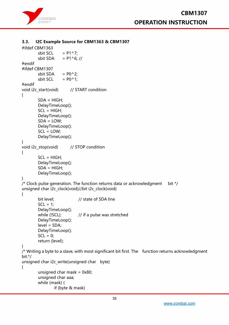
3.3. I2C Example Source for CBM1363 & CBM1307#ifdef CBM1363
sbit SCL = P1^7;sbit SDA = P1^6; //
#endif#ifdef CBM1307
sbit SDA = P0^2;sbit SCL = P0^1;
#endifvoid i2c_start(void) // START condition{
SDA = HIGH;DelayTimeLoop();SCL = HIGH;DelayTimeLoop();SDA = LOW;DelayTimeLoop();SCL = LOW;DelayTimeLoop();
}void i2c_stop(void) // STOP condition{
SCL = HIGH;DelayTimeLoop();SDA = HIGH;DelayTimeLoop();
}/* Clock pulse generation. The function returns data or acknowledgment bit */unsigned char i2c_clock(void)//bit i2c_clock(void){
bit level; // state of SDA lineSCL = 1;DelayTimeLoop();while (!SCL); // if a pulse was stretchedDelayTimeLoop();level = SDA;DelayTimeLoop();SCL = 0;return (level);
}/* Writing a byte to a slave, with most significant bit first. The function returns acknowledgmentbit.*/unsigned char i2c_write(unsigned char byte){
unsigned char mask = 0x80;unsigned char aaa;while (mask) {
if (byte & mask)
36
www.corebai.com
CBM1307
OPERATION INSTRUCTION
SDA = 1;else
SDA = 0;i2c_clock();mask >>= 1;
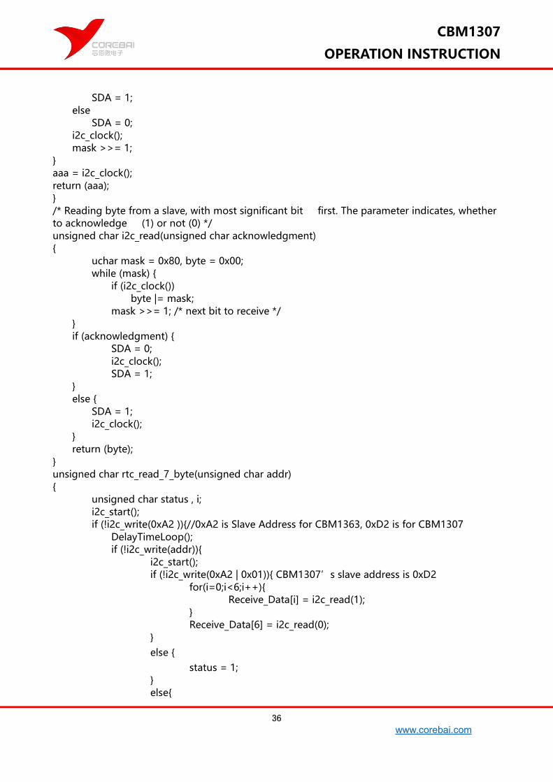
}aaa = i2c_clock();return (aaa);}/* Reading byte from a slave, with most significant bit first. The parameter indicates, whetherto acknowledge (1) or not (0) */unsigned char i2c_read(unsigned char acknowledgment){
uchar mask = 0x80, byte = 0x00;while (mask) {
if (i2c_clock())byte |= mask;
mask >>= 1; /* next bit to receive */}if (acknowledgment) {
SDA = 0;i2c_clock();SDA = 1;
}else {
SDA = 1;i2c_clock();
}return (byte);
}unsigned char rtc_read_7_byte(unsigned char addr){
unsigned char status , i;i2c_start();if (!i2c_write(0xA2 )){//0xA2 is Slave Address for CBM1363, 0xD2 is for CBM1307
DelayTimeLoop();if (!i2c_write(addr)){
i2c_start();if (!i2c_write(0xA2 | 0x01)){ CBM1307’s slave address is 0xD2
for(i=0;i<6;i++){Receive_Data[i] = i2c_read(1);
}Receive_Data[6] = i2c_read(0);
}else {
status = 1;}else{
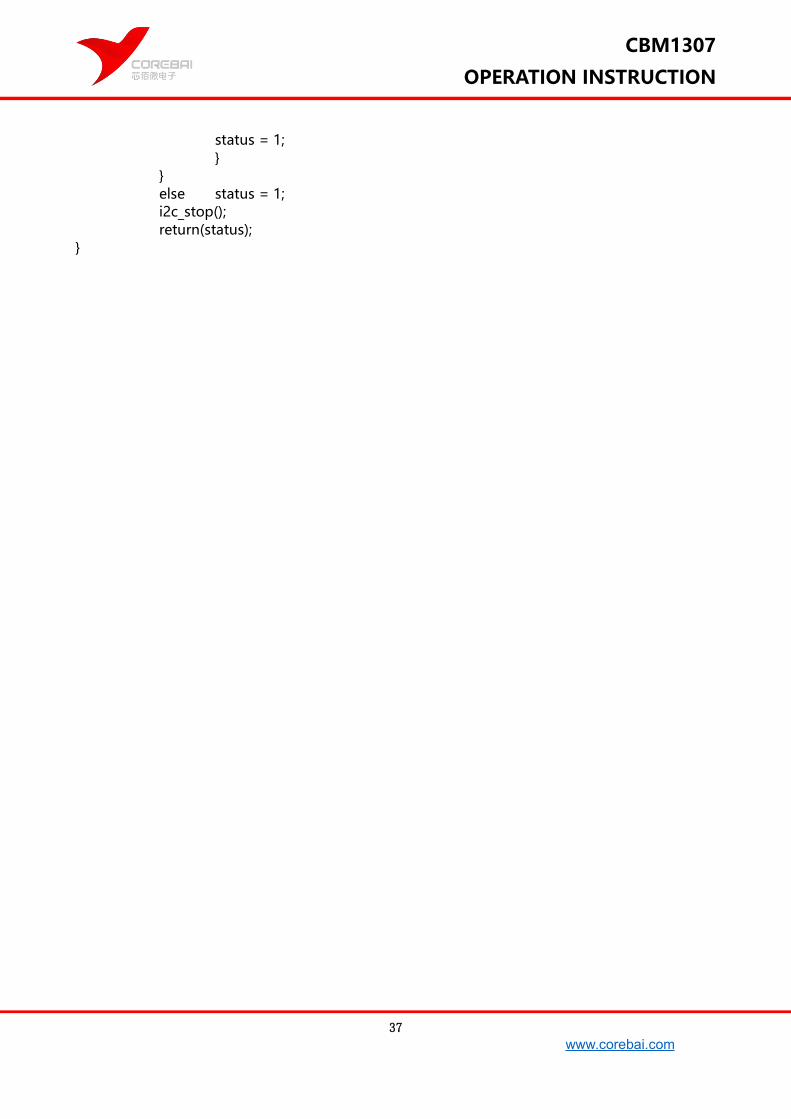
37
www.corebai.com
CBM1307
OPERATION INSTRUCTION
status = 1;}
}else status = 1;i2c_stop();return(status);
}

38
www.corebai.com
CBM1307
OPERATION INSTRUCTION
4. Test Procedure for RTC
4.1. Test Procedure for CBM1363
1. Make sure that test fixture is power off.
2. Place CBM1363 on CBM1363_SOCKET of test fixture.
3. Connect the Battery on CBM1363_BAT.
4. Run the Serial terminal and make sure the baud rate is set correctly at 9600bps
5. After turning on the power of test fixture, identify whether Green LED of Status Indicator is
flickering. If that’s flickering every 1S, it indicates CBM1363 working . Method for the
program is refer to the Chapter 2.
6. Data is displayed in Serial Terminal window like to Fig6. refer to Fig6
7. And then test fixture is power off.
8. Wait for a period of time ( two hours, 10 minutes, etc .).
9. Turn the test fixture on again, and check the time. the amount time as power off is passed .
4.2. Test Procedure for CBM1307
1. Make sure that test fixture is power off.
2. Place CBM1363 on CBM1307_SOCKET of test fixture.
3. Connect the Battery on CBM1307_BAT.
4. Run the Serial terminal and make sure the baud rate is set correctly at 9600bps
5. After turning on the power of test fixture, identify whether Green LED of Status Indicator is
flickering. If that’s flickering every 1S, it indicates CBM1307 working . Method for the
program is refer to the Chapter 2.
6. Data is displayed in Serial Terminal window like to Fig7. refer to Fig7
7. And then test fixture is power off.
8. Wait for a period of time ( two hours, 10 minutes, etc .).
9. Turn the test fixture on again, and check the time. the amount time as power off is passed .