catalogue - vigo€¦ · · 2017-01-13custom engineering / design ... the current that flows in a...
TRANSCRIPT

Catalogue

TABLE OF CONTENTS• Symbols............................................................................................................................................................... 3• Glossary of Terms................................................................................................................................................ 4
◦ General Definitions........................................................................................................................................ 4◦ Detector Parameters...................................................................................................................................... 4◦ Preamplifier Parameters................................................................................................................................ 5
• Application Notes................................................................................................................................................. 6◦ Thermoelectric Cooling.................................................................................................................................. 6◦ Thermoelectric Cooler Controllers................................................................................................................. 6◦ NCP03XM222E05RL Thermistor Characteristic............................................................................................7◦ Optical Immersion.......................................................................................................................................... 8◦ Preamplifiers for IR Detectors........................................................................................................................ 9◦ IR Detectors Packages................................................................................................................................ 10◦ IR Windows.................................................................................................................................................. 10◦ Applications................................................................................................................................................. 10◦ Custom Engineering / Design......................................................................................................................11◦ Precautions for Use..................................................................................................................................... 11
• Order Code........................................................................................................................................................ 12• Infrared Detectors.............................................................................................................................................. 15
◦ Photoconductors.......................................................................................................................................... 17◦ Photoelectromagnetic Detectors..................................................................................................................26◦ Photovoltaic Detectors................................................................................................................................. 28
• Infrared Detectors Accessories..........................................................................................................................42◦ Preamplifiers................................................................................................................................................ 44◦ TEC Controllers........................................................................................................................................... 72◦ Preamplifier Power Supplies........................................................................................................................ 80◦ Cables......................................................................................................................................................... 86◦ AC Adaptors................................................................................................................................................. 87◦ Mechanical Accessories.............................................................................................................................. 87
• Warranty............................................................................................................................................................. 94• Contact and Distributors..................................................................................................................................... 95• Appendix............................................................................................................................................................ 96
VIGO System S.A. 129/133 Poznanska St., 05-850 Ozarow Mazowiecki, Poland, tel.: +48 22 733 54 10, fax: +48 22 733 54 26, email: [email protected] 2Please note: the information contained in the document is subject to change without further notification. VIGO System S.A. reserves the right to alter the performance and any resulting specifications. VS 13.01.17 KO

SYMBOLS
A detector active area tr rise time
Cd detector capacitance tup power-on to LOCK indicator time
D* normalized detectivity w width of the detector
en preamplifier input noise voltage density Vn noise voltage
fo noise measurement frequency Vout output voltage swing
fhi high cut-off frequency Voff output voltage offset
flo low cut-off frequency Vsup power supply voltage
I current VTEC maximum TEC output voltage
Ib bias current Zd detector impedance
Idark dark current λpeak peak wavelength [μm]
Iin total input noise current λopt optimal wavelength [μm]
In noise current λcut-on cut-on wavelength [μm]
in noise current density λcut-off cut-off wavelength [μm]
Isup power supply current τ time constant [ns]
ITEC maximum TEC output current
I' current flowing through detector resistance
IR infrared:
MWIR – Mid-Wavelength Infrared: 2-6 µm
LWIR – Long-Wavelength Infrared: 8-14 µm
k Boltzmann's constant: 1.3806·10-23 J/K
Ki transimpedance
PC photoconductor
PCI photoconductor optically immersed
PCQ quadrant photoconductor
PEM photoelectromagnetic detector
PV photovoltaic detector
PVI photovoltaic optically immersed detector
PVM photovoltaic multiple junction detector
PVMI photovoltaic multiple junction detector optically immersed
PVMQ quadrant photovoltaic multiple junction detector
R detector resistance
Ri current responsivity
RL load resistance
Rout output impedance
Rs series resistance
Rsq sheet resistance
Rv voltage responsivity
Ta ambient temperature
VIGO System S.A. 129/133 Poznanska St., 05-850 Ozarow Mazowiecki, Poland, tel.: +48 22 733 54 10, fax: +48 22 733 54 26, email: [email protected] 3Please note: the information contained in the document is subject to change without further notification. VIGO System S.A. reserves the right to alter the performance and any resulting specifications. VS 13.01.17 KO

GLOSSARY OF TERMS
General DefinitionsHg1-xCdxTeKnown also as Mercury Cadmium Telluride (MCT), CdHgTe, (Cd,Hg)Teor MerCadTel; an alloy of CdTe and HgTe. Change of the CdTe toHgTe ratio (composition or x-value) can be used to tune opticalabsorption cut-off wavelength in the wide range from ultraviolet (UV) todeep infrared (IR). Cooling shifts the cut-off wavelength towards longwavelengths. Detectors from VIGO System are based on complexgraded gap MCT structures optimized for MWIR (3-6 µm) and LWIR(8-14 µm) ranges.
Detector FormatsSquare and rectangular formats are used for PC, PV, PVM and PEMdetectors.Circular shapes for some PV detectors are available upon request.
Photoelectromagnetic Detectors (PEM)Photovoltaic Detectors based on the Photoelectromagnetic Effect. Itconsists in spatial separation of optically generated electrons andholes in the magnetic field. They do not require electrical bias andshow no flicker noise (1/f).The PEM devices are typically used as fast, uncooled detectors of thelong wavelength radiation.
Photovoltaic Detectors (PV, PVM)Photovoltaic Detectors (photodiodes) are semiconductor structureswith one (PV) or multiple (PVM) homo- or heterojunctions. Absorbedphotons produce electron-hole pairs, resulting in external photocurrent.Reverse bias voltage may be applied to increase differentialresistance, reduce the shot noise, improve high frequencyperformance and dynamic range.Reverse bias may increase responsivity in some devices.Unfortunately, at the expense of flicker noise (1/f) in most cases.Photovoltaic detectors are more vulnerable to electrostaticdischarges than Photoconductors.
Photoconductors (PC)Photoconductive Detectors based on the Photoconductive Effect.Infrared radiation generates charge carriers in the semiconductoractive region decreasing its resistance. The resistance change issensed as a voltage change by applying a constant current bias. Theoptimum bias current is specified in the Final Test Report anddepends on the detector size, operating temperature and spectralcharacteristics
Detector ParametersCurrent and Voltage Responsivity: Ri, Rv
Ri(λ )=CurrentSignal (λ)⋅dλ
Incident Power(λ)⋅d λ [ AW ]
Current responsivity is typically used for description of PV and PVMdetectors.
Ri(λ )=VoltageSignal(λ)⋅dλ
Incident Power(λ)⋅d λ [ VW ]
Voltage responsivity is typically used for description of PC and PEMdetectors.
Responsivity-Width Product: Ri·w, Rv·wThe responsivity of PC, PEM and PVM devices is inverselyproportional to the width w of the detector.Therefore, the normalized responsivity can be expressed as thecurrent responsivity-width product (Ri·w) for PVM or voltageresponsivity-width product (Rv·w) for PC and PEM.
Dark Current: Idark
The current that flows in a photodetector when it is not receiving anylight. It may increase as the temperature rises.The small amount of current that flows through a photonicsemiconductor device when it is not operating. Also known asLeakage Current.
Maximum Bias Current: Imax
The maximum current that can flow through a Photoconductive orPhotovoltaic detector without a risk of its damage.
Bias Current-Width Ratio: Ib/wWidth-normalized photoconductor bias current.Typical Photoconductor's (PC series) bias current Ib should beincreased proportionally to it's width w. Therefore, the normalized biascurrent can be expressed as the Ib/w.
Noise Current and Noise Voltage: In, Vn
Root mean square Noise Current or Noise Voltage.
In=√ In2(t ) Vn=√Un
2(t)
Noise Current and Noise Voltage Density: in, vn
in=In
√Δ f vn=
Vn
√Δ f
Corner Frequency: 1/fFlicker noise or 1/f noise is a frequency dependent noise.
Its power is proportional to 1
fb where b ~ 1.
Below the corner frequency the noise of detectors is dominated byflicker noise.
Normalized Detectivity: D*The Signal-to-Noise Ratio (SNR) at a detector output normalized to1 W radiant power, a 1 cm2 detector optical area and a 1 Hzbandwidth.The higher the D* value, the better the detector.
D*=Ri
in√A=
R v
vn
√A [ cm⋅√HzW ]
Optical Area: AActive Area (Active Element) - the area from which the incidentradiant power is collected.For immersed detector it is different from physical detector area (seeOptical Immersion chapter).
Detector Capacitance: Cd
Parallel capacitance in the detector structure.
Spectral ResponseSpectral Responsivity or Spectral Detectivity – in detector data sheetsit is presented as Rv(λ), Ri(λ) or D*(λ).It can be characterized by cut-on, cut-off, optimum and peakwavelength.
Peak Wavelength: λpeak
λpeak is a wavelength of detector maximum responsivity.
Optimum Wavelength: λopt
The wavelength a device is optimized for. Typically longer than λpeak.
Cut-On Wavelength: λcut-on
λcut-on is the shortest wavelength at which a detector responsivityreaches 10% of the peak value.
Cut-Off Wavelength: λcut-off
λcut-off is the longest wavelength at which a detector responsivityreaches 50% of the peak value.
VIGO System S.A. 129/133 Poznanska St., 05-850 Ozarow Mazowiecki, Poland, tel.: +48 22 733 54 10, fax: +48 22 733 54 26, email: [email protected] 4Please note: the information contained in the document is subject to change without further notification. VIGO System S.A. reserves the right to alter the performance and any resulting specifications. VS 13.01.17 KO

Glossary of Terms
Resistance – Optical Area Product: R·AArea-normalized detector resistance. Typical photodiodes (PV)resistance decreases proportionally to their area increasing. Therefore,the normalized resistance can be expressed as the R·A.In contrast, the PVM detectors are characterized by SheetResistance.
Series Resistance: Rs
Parasitic resistance in photodiodes. Its contribution to the total dioderesistance may be significant for long wavelength and near roomOperating Temperatures diodes, especially with large Optical Area.
Sheet Resistance: Rsq
The normalized resistance expressed in Ω/□. It is used to normalizethe resistance for different size devices with non-square active area
Rsq=R⋅w
l
Time Constant: τTypically, detector time response can be described by one pole filter.Time Constant is the time it takes detector to reach 1/e ≈ 37% of theinitial signal value.Time Constant is related to the 3dB High Cut-Off Frequency fhi:
τ=1
(2 π f hi)
Time Constant is related to 10 – 90% Rise Time tr:t r=2.2 τ
Operating Temperature: TDetector active element temperature.
Acceptance Angle: ΦAcceptance angle is the maximum angle at which incoming radiationcan be captured by a detector. Radiation coming from a larger coneangle won't reach the detector.
Field of View: FOVVIGO defines the Field of View as the angle (FOV), which is two timesthe half angle defined by:
• the center of the detector and detector housing - in flat orequipped with hemispherical lens detectors,
and• the marginal ray in detectors with intermediate or
hyperhemispherical (standard) lens.In systems without external objectives Acceptance Angle and FOV areidentical.
F-number: F/#F/# is related to the image-space acceptance angle when the system isfocused at infinity.
Preamplifier ParametersOutput Voltage Responsivity: RV
The output voltage divided by optical power incident on the detector.
Output Voltage Swing: Vout
The maximum and minimum voltages where preamplifier works inlinear range.
GNDPoint of zero potential. For standard preamplifiers is common powersupply and signal ground.
Low Cut-Off Frequency: flo
A minimum frequency at which a module responsivity (or preamplifiergain) reaches -3dB of the peak value.
High Cut-Off Frequency: fhi
A maximum frequency at which a module responsivity (or preamplifiergain) reaches -3dB of the peak value.
Output NoiseNoise voltage at preamplifier output.
Average Output Noise Density:
Vn=√∫f 1
f 2
Vout2
(f )df
f 2−f 1
Noise Measurement Frequency: f0
Frequency at which output voltage noise is measured selectively.
Output Noise Density at Specific Frequency: Vn(f0)Noise voltage density measured at a given frequency.
Transimpedance: Ki
Current to voltage conversion factor (ratio).
Ki=Vout
Iin
Preamplifier Input Noise Current: in
Noise current generated by equivalent current source in parallel withideal preamplifier input.
Preamplifier Input Noise Voltage: en
Noise voltage generated by equivalent voltage source in series withideal preamplifier input.
Total Input Noise Current: Iin
Parameter taking into consideration all noise sources related to theinput.
Iin=√(iPA2 +id
2)=Vn0
Tr
Output Impedance: Rout
Equivalent impedance exhibited by its output terminals.
Load Resistance: RL
Optimal resistance of the load: amplifier's or the measurementdevice's.
Output Voltage Offset: Voff
DC component of the output voltage.
Power Supply Voltage: Vsup
Supply voltage required for correct preamplifier operation. ±20%tolerance is allowed.
Power Supply Current: Isup
Supply current consumption during correct preamplifier operation.
Coupling TypePreamplifier coupling type. It may be AC for alternate current or DC fordirect current.
Power Supply Input (+) and (-)Polarity of the power supply related to the ground. Swapping supplyconnectors may lead to module damage.
VIGO System S.A. 129/133 Poznanska St., 05-850 Ozarow Mazowiecki, Poland, tel.: +48 22 733 54 10, fax: +48 22 733 54 26, email: [email protected] 5Please note: the information contained in the document is subject to change without further notification. VIGO System S.A. reserves the right to alter the performance and any resulting specifications. VS 13.01.17 KO

APPLICATION NOTES
ThermoElectric Cooling (TEC)
Detector cooling reduces noise, increases responsivity and, in somedevices, improves high frequency response. Two-, three- andfour-stage TE coolers are available. TEC is biased with DC power. Allspecifications are given for 300 K heat sink temperature.
TEC are characterized by:
Maximum Temperature Difference: ΔTmax
ΔTmax rated at Q=0, at other Q the ΔT should be estimated asΔT=ΔTmax(1-Q/Qmax).
Optimum Current: Iopt
Supply current giving the highest temperature difference (ΔTmax) at thespecified conditions stated in Detector Final Test Report.
Maximum TEC Voltage: Vmax
Voltage drop at ΔTmax.
Maximum Heat Pumping Capacity: Qmax
Qmax rated at ΔT=0, at other ΔT cooling capacity should be estimatedas Q=Q max(1-ΔT/ΔTmax)
Standard TEC Parameters
Parameter Unit 2TE 3TE 4TETdet K ~230 ~210 ~195Vmax V 1.3 3.6 8.3Imax A 1.2 0.45 0.5Qmax W 0.36 0.27 0.28ΔTmax K 92 114 125
Temperature SensorThe built-in thermistor serves as a sensor of the detector operationtemperature. TE-cooled detectors are equipped with thermistor typeNCP03XM222E05RL as a standard.
Heat SinkingSuitable heat sinking is necessary to dissipate heat generated bythe Peltier cooler or excessive optical irradiation. Since heat is almost100% dissipated at the base of the detector housing, it must be firmlyattached to the heat sink (Figures a and b). Heat sinking via themounting screw or via the detector housing cylindrical walls is notsufficient (Figures c and d). A thin layer of heat conductive epoxy orsilicone grease should be applied to improve thermal contact betweendetector housing and heat sink.A heat sink thermal resistance of ~2 K/W is typically required for themost two- and three-stage Peltier coolers. Four-stage cooler requires~1 K/W.
Figures. Heat dissipation from TE-cooled detector
ThermoElectric Cooler Controllers (TECC)
VIGO System offers the standard TEC controller STCC-04,the miniature TEC controller MTCC-01 and programmable “smart”TEC controllers PTCC-01 (available options: OEM, Basic andAdvanced).
Temperature Sensor InputsTemperature sensor pins – might be connected with any polarity.
TEC Supply Input (+) and (-)Supply polarity for the TEC. Those pins are floating, which means theyare not connected to the GND.
Maximum TEC Controller Output Current: ITEC
Maximum current that is provided by the controller to the TEC.
Maximum TEC Controller Output Voltage: VTEC
Maximum voltage that is provided by the controller to the TEC.
Ripple of Output CurrentIt is a small unwanted residual periodic variation of the DC (directcurrent) output of a power supply (or other device) which has beenderived from an AC (alternating current) source. This ripple is due toincomplete suppression of the rectified DC waveform within the powersupply.
Output Current of the Built-In Power SupplyMaximum current that can be delivered by power supply to thepreamplifier, usually +/-100 mA.
Series Resistance of the Connecting CableMaterial parameter - resistance of the supply cable. It depends oncable length.
Settling Time of the Set Detector TemperatureThe time taken by the cooling system to reach appropriatetemperature of the detector.
Maximum Voltage Across TEC ElementMaximum voltage for TEC supplying.
VIGO System S.A. 129/133 Poznanska St., 05-850 Ozarow Mazowiecki, Poland, tel.: +48 22 733 54 10, fax: +48 22 733 54 26, email: [email protected] 6Please note: the information contained in the document is subject to change without further notification. VIGO System S.A. reserves the right to alter the performance and any resulting specifications. VS 13.01.17 KO
c
ba
YES
NONO
d
YES

Application Notes
NCP03XM222E05RL Thermistor Characteristic
The electricity applied to between terminals of thermistors should beunder the maximum power dissipation at 25 °C (100 mW) not todestroy the thermosensor. For the measurement of resistance, thepower should not exceed 1 mW.The relation between the resistance and the temperature:
RT=RT0⋅exp (β⋅T0−T
T⋅T0
)
Values for NCP03XM222E05RL thermistor:• RT0 = 2.2 kΩ ± 3% at T0 = 298 K;
180 190 200 210 220 230 240 250 260 270 280 290 300
0
200
400
600
800
1000
1200
1400
1600
1800
2000 Rmin, kOhm
Rnom, kOhm
Rmax, kOhm
Temperature [K]
Th
erm
isto
r re
sis
tan
ce [
kOh
m]
T [K]
180 -93 1594,97 1757,95 1935,84
182 -91 1336,02 1469,90 1615,75
184 -89 1124,16 1234,66 1354,81
186 -87 950,46 1042,11 1141,58
188 -85 807,57 883,99 966,78
190 -83 689,57 753,62 822,88
192 -81 591,68 645,64 703,89
194 -79 510,07 555,75 604,98
196 -77 441,68 480,54 522,34
198 -75 384,05 417,25 452,91
200 -73 335,23 363,71 394,26
202 -71 293,65 318,17 344,43
204 -69 258,05 279,23 301,88
206 -67 227,41 245,76 265,36
208 -65 200,91 216,85 233,85
210 -63 177,89 191,77 206,55
T [oC] Rmin [kΩ] Rnom [kΩ] Rmax [kΩ]
Resistance vs Temperature for NCP03XM222E05RLThermistor
T [K]
212 -61 157,81 169,92 182,79
214 -59 140,22 150,80 162,03
216 -57 124,76 134,02 143,83
218 -55 111,14 119,25 127,83
220 -53 99,10 106,21 113,72
222 -51 88,44 94,67 101,25
224 -49 78,98 84,44 90,21
226 -47 70,57 75,37 80,42
228 -45 63,09 67,30 71,73
230 -43 56,42 60,12 64,01
232 -41 50,49 53,74 57,15
234 -39 45,19 48,05 51,04
236 -37 40,47 42,98 45,61
238 -35 36,26 38,47 40,77
240 -33 32,51 34,45 36,47
242 -31 29,16 30,87 32,64
244 -29 26,18 27,68 29,24
246 -27 23,51 24,84 26,21
248 -25 21,14 22,30 23,51
250 -23 19,02 20,05 21,11
252 -21 17,13 18,04 18,98
254 -19 15,45 16,25 17,07
256 -17 13,95 14,65 15,38
258 -15 12,61 13,23 13,87
260 -13 11,41 11,96 12,53
262 -11 10,34 10,83 11,33
264 -9 9,38 9,82 10,26
266 -7 8,52 8,91 9,31
268 -5 7,75 8,10 8,45
270 -3 7,07 7,37 7,69
272 -1 6,45 6,72 7,00
274 1 5,89 6,13 6,38
276 3 5,38 5,60 5,83
278 5 4,93 5,13 5,32
280 7 4,52 4,69 4,87
282 9 4,15 4,30 4,46
284 11 3,81 3,95 4,09
286 13 3,50 3,63 3,75
288 15 3,22 3,33 3,45
290 17 2,96 3,06 3,17
292 19 2,73 2,82 2,91
294 21 2,51 2,59 2,68
296 23 2,32 2,39 2,46
298 25 2,13 2,20 2,27
T [oC] Rmin [kΩ] Rnom [kΩ] Rmax [kΩ]
VIGO System S.A. 129/133 Poznanska St., 05-850 Ozarow Mazowiecki, Poland, tel.: +48 22 733 54 10, fax: +48 22 733 54 26, email: [email protected] 7Please note: the information contained in the document is subject to change without further notification. VIGO System S.A. reserves the right to alter the performance and any resulting specifications. VS 13.01.17 KO

Application Notes
Optical Immersion
Optical immersion is achieved by using high refractive indexmicrolenses in order to improve performance of the devices but maylimit acceptance angle.
Optical immersion is monolithic integration of detector element withhyperhemispherical microlens (basic configuration) that makes opticalsize of detector 11 times larger compared to its physical size. Thisresults in improvement of D* by one order of magnitude and electriccapacitance by a factor of two orders of magnitude less compared toconventional detector of the same optical area.Function and properties of hemispherical and hyperhemisphericallenses are illustrated in the Figure and the Table below.
Parameter SymbolHemisphere Hyperhemisphere
Theory GaAs Theory GaAs
Distance L R R R(n+1) 4.3R
-dd'
n 3.3 n2 10.9
-Dimm
*
D*non−imm
n 3.3 n2 10.9
AcceptanceAngle
Φ 180° 180° 2arcsin(1/n) 35°
F/# - 0.5 0.5 n/2 1.62
Table. Immersed Detectors Parameters
n – a refractive index of a lens material (~3.3 for GaAs used by VIGO)d – optical (apparent) detector sized' – physical detector sizeR – lens radiusL – lens face to objective focal plane distance
h=R+Rn
- lens thickness
The values in the above Table show the relative change of a givenparameter comparing to a non-immersed detector of the same opticalsize.Detectors with custom acceptance angles are available uponrequest.
Immersion Technology is described in “Infrared Detectors andSystems”, E.L. Dereniak and G.D. Boreman, Wiley Interscience, 2000.
Figure. Function and properties of hemispherical and hyperhemispherical lense
VIGO System S.A. 129/133 Poznanska St., 05-850 Ozarow Mazowiecki, Poland, tel.: +48 22 733 54 10, fax: +48 22 733 54 26, email: [email protected] 8Please note: the information contained in the document is subject to change without further notification. VIGO System S.A. reserves the right to alter the performance and any resulting specifications. VS 13.01.17 KO
in
en
Rd
Cd
Cf
Rf
Iph
VO
Application Notes
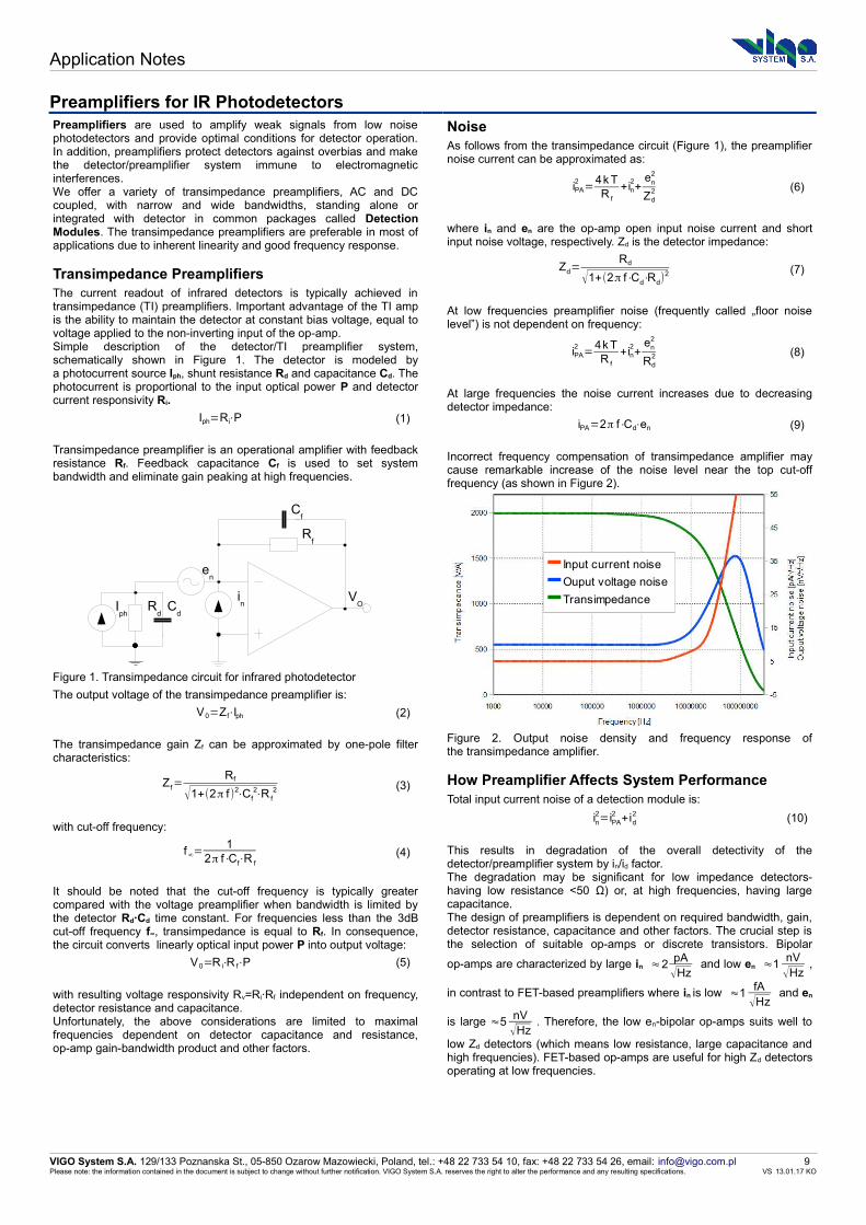
Preamplifiers for IR PhotodetectorsPreamplifiers are used to amplify weak signals from low noisephotodetectors and provide optimal conditions for detector operation.In addition, preamplifiers protect detectors against overbias and makethe detector/preamplifier system immune to electromagneticinterferences.We offer a variety of transimpedance preamplifiers, AC and DCcoupled, with narrow and wide bandwidths, standing alone orintegrated with detector in common packages called DetectionModules. The transimpedance preamplifiers are preferable in most ofapplications due to inherent linearity and good frequency response.
Transimpedance PreamplifiersThe current readout of infrared detectors is typically achieved intransimpedance (TI) preamplifiers. Important advantage of the TI ampis the ability to maintain the detector at constant bias voltage, equal tovoltage applied to the non-inverting input of the op-amp.Simple description of the detector/TI preamplifier system,schematically shown in Figure 1. The detector is modeled bya photocurrent source Iph, shunt resistance Rd and capacitance Cd. Thephotocurrent is proportional to the input optical power P and detectorcurrent responsivity Ri.
Iph=Ri⋅P (1)
Transimpedance preamplifier is an operational amplifier with feedbackresistance Rf. Feedback capacitance Cf is used to set systembandwidth and eliminate gain peaking at high frequencies.
Figure 1. Transimpedance circuit for infrared photodetector
The output voltage of the transimpedance preamplifier is:
V0=Z f⋅Iph (2)
The transimpedance gain Zf can be approximated by one-pole filtercharacteristics:
Zf=Rf
√1+(2π f)2⋅Cf2⋅R f
2 (3)
with cut-off frequency:
f∞=1
2π f⋅Cf⋅R f(4)
It should be noted that the cut-off frequency is typically greatercompared with the voltage preamplifier when bandwidth is limited bythe detector Rd∙Cd time constant. For frequencies less than the 3dBcut-off frequency f∞, transimpedance is equal to Rf. In consequence,the circuit converts linearly optical input power P into output voltage:
V0=R i⋅R f⋅P (5)
with resulting voltage responsivity Rv=Ri∙Rf independent on frequency,detector resistance and capacitance.Unfortunately, the above considerations are limited to maximalfrequencies dependent on detector capacitance and resistance,op-amp gain-bandwidth product and other factors.
NoiseAs follows from the transimpedance circuit (Figure 1), the preamplifiernoise current can be approximated as:
iPA2
=4k TR f
+ in2+
en2
Zd2 (6)
where in and en are the op-amp open input noise current and shortinput noise voltage, respectively. Zd is the detector impedance:
Zd=Rd
√1+(2π f⋅Cd⋅Rd)2 (7)
At low frequencies preamplifier noise (frequently called „floor noiselevel”) is not dependent on frequency:
iPA2
=4k TR f
+ in2+
en2
Rd2 (8)
At large frequencies the noise current increases due to decreasingdetector impedance:
iPA=2π f⋅Cd⋅en (9)
Incorrect frequency compensation of transimpedance amplifier maycause remarkable increase of the noise level near the top cut-offfrequency (as shown in Figure 2).
Figure 2. Output noise density and frequency response ofthe transimpedance amplifier.
How Preamplifier Affects System PerformanceTotal input current noise of a detection module is:
in2=iPA
2 + id2 (10)
This results in degradation of the overall detectivity of thedetector/preamplifier system by in/id factor.The degradation may be significant for low impedance detectors-having low resistance <50 Ω) or, at high frequencies, having largecapacitance.The design of preamplifiers is dependent on required bandwidth, gain,detector resistance, capacitance and other factors. The crucial step isthe selection of suitable op-amps or discrete transistors. Bipolar
op-amps are characterized by large in ≈2 pA
√Hz and low en ≈1
nV
√Hz,
in contrast to FET-based preamplifiers where in is low ≈1fA
√Hz and en
is large ≈5 nV√Hz
. Therefore, the low en-bipolar op-amps suits well to
low Zd detectors (which means low resistance, large capacitance andhigh frequencies). FET-based op-amps are useful for high Zd detectorsoperating at low frequencies.
VIGO System S.A. 129/133 Poznanska St., 05-850 Ozarow Mazowiecki, Poland, tel.: +48 22 733 54 10, fax: +48 22 733 54 26, email: [email protected] 9Please note: the information contained in the document is subject to change without further notification. VIGO System S.A. reserves the right to alter the performance and any resulting specifications. VS 13.01.17 KO
Input current noise
Ouput voltage noise
Transimpedance

Application Notes
IR Detectors Packages Applications
VIGO detectors are mounted in several packages (please see Tablebelow).The packages are filled with dry, heavy noble gases for low thermalconductivity (Kr/Xe mixtures). Water vapor condensation is preventedby careful sealing and water absorbers applied inside the package.
Package Detector Type
TO8 PC*), PCI*), PV*), PVI*), PVM*), PVMI*),PC-nTE, PCI-nTE, PV-nTE, PVI-nTE,
PVM-nTE, PVMI-nTE,PCQ, PVMQ
TO39PC, PCI, PV, PVI, PVM, PVMI
BNC
PC, PCI, PV, PVI, PVM, PVMI
PEM
PEM, PEMI
Quadrant*)
PCQ, PVMQ
*) Upon special request.For detailed information please see Appendix – Technical Drawings.
The typical applications of the VIGO System S.A. detectors are givenin the Table below. Please, provide detailed system requirements –our Engineering Team recommend optimum solution.
Applications Detector Series - Examples
Spectroscopy PCI-2TE, PVI-nTE, PVI, PCI
Positioning Systems PV, PV-2TE
Laser MetrologyPV, PV-2TE, PVM, PVM-2TE, PEM,
PEMI
High Speed Operation PVI-nTE, PVI, PVM, PVMI, PEM, PEMI
Analysis of Spatial andTime Distribution of Laser
BeamPV, PV-nTE, PVM, PVM-nTE
Remote TemperatureMeasurements
PV-nTE, PVI-nTE, PVI-nTE, PCI,PCI-nTE
Heterodyne Detection PV-2TE, PVI-nTE, PCI, PCI-nTE
Biomedical Applications PV, PVI-nTE, PVM, PVMI, PEM, PEMI
Pyrometers, Scanners PV-2TE, PVI-nTE, PCI, PCI-nTE
Thermal Imagers PV-2TE, PVI-nTE, PCI, PCI-nTE
Gas Analysis PCI-2TE, PVI-nTE, PVI, PCI
LIDAR PVI-nTE, PCI-nTE
Detection and Monitoringof Thermal Objects
PV-2TE, PVI-nTE PCI, PCI-nTE
Laser-Matter InteractionStudies
PV, PV-2TE, PVM, PVM-2TE, PEM,PEMI
Fire, Flame and HumanBody Detection
PV-2TE, PVI-nTE, PCI, PCI-nTE
Free Space OpticalCommunication
PVI-nTE, PVI
Laser Threat Warning PCI, PVI, PVMI
Tracking Systems PV, PV-2TE, PC, PCI, PCI-2TE, PC-2TE
Nondestructive MaterialTesting
All Devices
IR Windows
VIGO TE cooled detectors are typically provided with:
• 3° wedged Al2O3 windows (wAl2O3)
• 3° wedged ZnSe AR coated windows (wZnSeAR)
3° wedge prevents “fringing” - interference from stray back reflections.
We offer windows optimized for different spectral bands also.Percentage of MWIR and LWIR radiation that can pass through VIGOdetector windows is presented in the Figures below. Windows can beanti-reflection (AR) coated on two surfaces.
It is possible to use windows provided by the User (upon request).
Figure. Percentage of IR radiation that can pass through the window.
VIGO System S.A. 129/133 Poznanska St., 05-850 Ozarow Mazowiecki, Poland, tel.: +48 22 733 54 10, fax: +48 22 733 54 26, email: [email protected] 10Please note: the information contained in the document is subject to change without further notification. VIGO System S.A. reserves the right to alter the performance and any resulting specifications. VS 13.01.17 KO

Application Notes
Custom Engineering / Design
On the following pages of this catalogue you will find detailedspecifications of devices that are currently offered by VIGO System.However, our Engineering Team - including engineers experienced inoptoelectronics, mechanical engineering and electronics is ready tohelp solve the most sophisticated and complex problems related toinfrared radiation detection & measurements.The technology developed at VIGO System is very flexible, permittingconstruction of devices for specific applications.
Precautions for Use
Operating TemperatureA detector should be operated at its optimal temperature given inthe Final Test Report (delivered with every device).
Maximum VoltageDo not operate the PV detector at higher bias voltages than suggestedin the Final Test Report (delivered with every device).
Be Careful Using Ohmmeters for PV Detectors!Standard ohmmeters may overbias and damage the detector. This isespecially true for small physical area or SWIR PV detectors. Bias of10 mV can be used for resistance measurements of any typeof detector.Ask for conditions of I-V plot measurements!
UsageDevices can operate in the 10% to 80 % humidity, in the -20 °C to+30 °C ambient temperature range. Operation at >30 °C ambientmay reduce performance for standard Peltier coolers..Ask for systems that can operate in the +30 °C to +80 °C ambienttemperature range.
StorageThe following conditions should be fulfilled for safe and reliableoperation of detector:
• store in dark place, 10% to 90% humidity and -20 °C to+50 °C temperature,
• avoid exposing to the direct sunlight and strong UV/VIS lightas this may result in degradation of the detectorperformance,
• avoid electrostatic discharges at leads therefore, the devicesshould be stored having leads shorted.
HandlingSome IR Window materials such as BaF2 are soft and brittle. Particularattention should be paid to not scratch a surface of the window.A damaged window may entirely degrade the detector performance.Excessive mechanical stress applied to the package itself or toa device containing the package may result in permanent damage.Peltier element inside thermoelectrically cooled detectors issusceptible to mechanical shocks. Great care should be taken whenhandling cooled detectors.
Cleaning WindowKeep the Window clean. Use a soft cotton cloth damped with isopropylalcohol and wipe off the surface gently if necessary.
Mechanical ShocksThe Peltier elements may be damaged by excessive mechanicalshock or vibration. Care is recommended during manipulations andnormal use. Drop impacts against a hard surface are particularlydangerous.
Shaping LeadsAvoid bending the leads at a distance less than 2 mm from a base ofthe package to prevent glass seal damage. When shaping the leads,maximum two right angle bends and three twists at the distanceminimum 6 mm from the base of the package.Keep the leads of the detecting element shorted when shaping!
Soldering LeadsIR detectors can be easily damaged by excessive heat. Special careshould be taken when soldering the leads. Usage of heat sinks ishighly recommended. Tweezers can be used for this purpose; whensoldering, clamp a lead at a place between the soldering iron and thebase of the package. To avoid destructive influence of ESD and otheraccidental voltages (e.g. from a non-grounded soldering iron) rules forhandling LSI integrated circuits should be applied to IR detectors too.Leads should be soldered at +370 °C or below within 5 s.
Beam Power LimitationsDamage thresholds, specified as integrated power of incomingradiation:
• for detectors without immersion lens irradiated withcontinuous wave (CW) or single pulse longer than 1 µsirradiance on the active area must not exceed 100 W/cm2.The irradiance of the pulse shorter than 1 µs must notexceed 1 MW/cm2,
• for optically immersed detectors irradiated with CW or singlepulse longer than 1 µs irradiance on the apparent opticalactive area must not exceed 2.5 W/cm2. The irradiance ofthe pulse shorter than 1 µs must not exceed 10 kW/cm2,
• for repeated irradiation with pulses shorter than 1 µs,the equivalent CW irradiation, average power overthe pulse - to - pulse period should be less than the CWdamage threshold according to equation:
( equivalent CWradiationpower)=( pulsepeak power
focus area )⋅( pulseduration)⋅(repetition
rate )Saturation thresholds vary by detector type and can be provided uponrequest.
VIGO System S.A. 129/133 Poznanska St., 05-850 Ozarow Mazowiecki, Poland, tel.: +48 22 733 54 10, fax: +48 22 733 54 26, email: [email protected] 11Please note: the information contained in the document is subject to change without further notification. VIGO System S.A. reserves the right to alter the performance and any resulting specifications. VS 13.01.17 KO

ORDER CODE
How to Compile Your Order Code?Different information such as detector type, optical immersion, numberof stages TE-cooler, the wavelength a detector is optimized for,dimensions of optical area, package type, window type and FOVcombine to create VIGO System's Detector Order Code.
Below, there are information needed to specify exactly the requireddetector.
Type Immersion - Cooling - λopt - Length x Width - Package Type - Window - FOV
Type Immersion - Cooling - λopt - ΦDiameter - Package Type - Window - FOV
Examples
PVI-2TE-5-0.1x0.1-TO8-wBaF2-35
PV I - 2TE - 5 - 0.1 x 0.1 - TO8 - wAl2O3 - 36
PEM-10.6-1x1-PEM-wBaF2-51
PEM - - 10.6 - 1 x 1 1 PEM - wZnSeAR - 51
PC-10.6-1x1-BNC-NoWindow-102
PC - - 10.6 - 1 x 1 1 BNC - NoWindow - 102
PVI-2TE-6-Φ0.05-TO8-pGeAR-60
PV I - 2TE - 6 - Φ0.05 - TO8 - pGeAR - 36
Detector Types
PC – photoconductor
PV – single junction photovoltaic detector
PVM – LWIR multiple junction photovoltaic detector
PEM – photoelectromagnetic detector
PCQ – quadrant photoconductor
PVMQ – quadrant LWIR multiple junction photovoltaic detector
Optical ImmersionAll detectors can be monolithically integrated with immersionmicrolens. Please add letter “I” to the end of Detector Type symbol forimmersed detectors. Hyperhemispherical immersion microlens isoffered as a standard.
TE CoolingVIGO PC, PV and PVM detectors are available as uncooled devices orequipped with multiple stage TE cooling. Please add “2TE”, “3TE” or“4TE” for two-, three-, or four stage TE cooled detectors respectively.
Wavelength Range and Optimum Wawalength λopt
VIGO standard detectors are optimized for specific wavelength (seeTable below). Other wavelengths are available as an option.
Detector Type Optimum Wavelength [μm]PC, PCI 4 5 6 9 10.6
PC-2TE, PCI-2TE 4 5 6 9 10.6 12 13
PC-3TE, PCI-3TE 9 10.6 12 13
PC-4TE, PCI-4TE 9 10.6 12 13 14
PV, PVI 3 3.4 4 5 6 8
PV-nTE, PVI-nTE 3 3.4 4 5 6 8 10.6
PVM, PVMI, PVM-nTE, PVMI-nTE 8 10.6
PEM, PEMI, PCQ, PVMQ 10.6
VIGO System S.A. 129/133 Poznanska St., 05-850 Ozarow Mazowiecki, Poland, tel.: +48 22 733 54 10, fax: +48 22 733 54 26, email: [email protected] 12Please note: the information contained in the document is subject to change without further notification. VIGO System S.A. reserves the right to alter the performance and any resulting specifications. VS 13.01.17 KO

Order Code
Optical Area Availability Table
Typical VIGO detectors are squared-shaped. Single junctionphotovoltaic devices are also available as a circular upon request.
Please specify dimension (length×width) for square or diameter (Φ) forcircular areas.
Detector Type Optical Area [mm×mm]0.025×0.025 0.05×0.05 0.1×0.1 0.2×0.2 0.25×0.25 0.5×0.5 1×1 2×2 3×3 4×4
PV-3 O X X O O OPV-2TE-3 O X X O O OPV-3TE-3 O X X O O OPV-4TE-3 O X X O O OPVI-3 O X X OPVI-2TE-3 O X X OPVI-3TE-3 O X X OPVI-4TE-3 O X X OPV-3.4 O X X O O OPV-2TE-3.4 O X X O O OPV-3TE-3.4 O X X O O OPV-4TE-3.4 O X X O O OPVI-3.4 O X X OPVI-2TE-3.4 O X X OPVI-3TE-3.4 O X X OPVI-4TE-3.4 O X X OPC-4 X X X X X X X X X XPC-2TE-4 X X X X X X X XPCI-4 X X X XPCI-2TE-4 X X X XPV-4 O X X O O OPV-2TE-4 O X X O O OPV-3TE-4 O X X O O OPV-4TE-4 O X X O O OPVI-4 O X X OPVI-2TE-4 O X X OPVI-3TE-4 O X X OPVI-4TE-4 O X X OPC-5 X X X X X X X X X XPC-2TE-5 X X X X X X X XPCI-5 X X X XPCI-2TE-5 X X X XPV-5 O X X O O OPV-2TE-5 O X X O O OPV-3TE-5 O X X O O OPV-4TE-5 O X X O O OPVI-5 O X X OPVI-2TE-5 O X X OPVI-3TE-5 O X X OPVI-3TE-5 O X X OPVI-4TE-5 O X X OPC-6 X X X X X X X X X XPC-2TE-6 X X X X X X X XPCI-6 X X X XPCI-2TE-6 X X X XPV-6 O X X O O OPV-2TE-6 O X X O O OPV-3TE-6 O X X O O OPV-4TE-6 O X X O O OPVI-6 O X XPVI-2TE-6 O X XPVI-3TE-6 O X XPVI-4TE-6 O X XPV-8 X X*) PPV-2TE-8 X X*) PPV-3TE-8 X X*) PPV-4TE-8 X X*) PPVI-8 X X*) PPVI-2TE-8 X X*) PPVI-3TE-8 X X*) PPVI-4TE-8 X X X*) PPVM-8 O O X X O O X X X XPVM-2TE-8 O O X X O O X X XPVMI-8 O O X XPVMI-2TE-8 O O X XPVMI-3TE-8 O O X XPVMI-4TE-8 O O X XPC-9 X X X X X X X X X XPC-2TE-9 X X X X X X X XPC-3TE-9 X X X X X X X XPC-4TE-9 X X X X X X X XPCI-9 X X X XPCI-2TE-9 X X X XPCI-3TE-9 X X X XPCI-4TE-9 X X X XPC-10.6 X X X X X X X X X XPC-2TE-10.6 X X X X X X X XPC-3TE-10.6 X X X X X X X XPC-4TE-10.6 X X X X X X X X
VIGO System S.A. 129/133 Poznanska St., 05-850 Ozarow Mazowiecki, Poland, tel.: +48 22 733 54 10, fax: +48 22 733 54 26, email: [email protected] 13Please note: the information contained in the document is subject to change without further notification. VIGO System S.A. reserves the right to alter the performance and any resulting specifications. VS 13.01.17 KO

Order Code
Detector Type Optical Area [mm×mm]0.025×0.025 0.05×0.05 0.1×0.1 0.2×0.2 0.25×0.25 0.5×0.5 1×1 2×2 3×3 4×4
PCI-10.6 X X X XPCI-2TE-10.6 X X X XPCI-3TE-10.6 X X X XPCI-4TE-10.6 X X X XPV-2TE-10.6 X X*) PPV-3TE-10.6 X X*) PPV-4TE-10.6 X X*) PPVI-2TE-10.6 X X*) PPVI-3TE-10.6 X X*) PPVI-4TE-10.6 X X*) PPVM-10.6 O O X X O O X X X XPVM-2TE-10.6 O O X X O O X X XPVMI-10.6 O O X XPVMI-2TE-10.6 O O X XPVMI-3TE-10.6 O O X XPVMI-4TE-10.6 O O X XPEM-10.6 O O O O X XPEMI-10.6 O O X XPCQ-10.6 X X X X X X X X XPC-2TE-12 X X X X X X X XPC-3TE-12 X X X X X X X XPC-4TE-12 X X X X X X X XPCI-2TE-12 X X X XPCI-3TE-12 X X X XPCI-4TE-12 X X X XPC-2TE-13 X X X X X X X XPC-3TE-13 X X X X X X X XPC-4TE-13 X X X X X X X XPCI-2TE-13 X X X XPCI-3TE-13 X X X XPCI-4TE-13 X X X XPC-4TE-14 X X X XPCI-4TE-14 X X X X
*) Devices may require reverse bias in order to increase dynamic resistance and improve frequency response.X – standard detector - operating without biasP – default - operating with reverse biasO – detectors available upon request, parameters may vary from these in data sheets
Package TypeVIGO detectors are typically offered in four different packages:
Package Type Detector TypeBNC, TO39 PC, PCI, PV, PVI, PVM, PVMI
TO8 PC-nTE, PCI-nTE, PV-nTE, PVI-nTE, PVM-nTE, PVMI-nTE, PCQ, PVMQPEM PEM, PEMI
Window Type
VIGO TE cooled detectors are typically provided with:• 3° wedged Al2O3 windows (wAl2O3)• 3° wedged ZnSe AR coated window (wZnSeAR)
Other Windows are available as following options:
MaterialHardness[kg/mm2]
AR Coating Symbol
BaF2 82 wedged no wBaF2
Si 1100wedged yes wSiARplanar yes pSiAR
ZnSe 120wedged yes wZnSeARplanar yes pZnSeAR
When no window is needed (for uncooled detectors), “NoWindow”attribute must be added.
MaterialHardness[kg/mm2]
AR Coating Symbol
Al2O3 1370wedged
yes wAl2O3ARno wAl2O3
planaryes pAl2O3ARno pAl2O3
Ge 780wedged yes wGeARplanar yes pGeAR
black – standard (without extra charge)red – nonstandard with extra charge
Field of View: FOVAngular field of view of detector in degrees [ °]. FOV depends on type of immersion microlens applied and package used for the detector. Fordetailed information please see Appendix – Technical Drawings.
VIGO System S.A. 129/133 Poznanska St., 05-850 Ozarow Mazowiecki, Poland, tel.: +48 22 733 54 10, fax: +48 22 733 54 26, email: [email protected] 14Please note: the information contained in the document is subject to change without further notification. VIGO System S.A. reserves the right to alter the performance and any resulting specifications. VS 13.01.17 KO

Infrared Detectors
VIGO System S.A. 129/133 Poznanska St., 05-850 Ozarow Mazowiecki, Poland, tel.: +48 22 733 54 10, fax: +48 22 733 54 26, email: [email protected] 15Please note: the information contained in the document is subject to change without further notification. VIGO System S.A. reserves the right to alter the performance and any resulting specifications. VS 13.01.17 KO
FeatureParameter
Optimal Wavelength λopt, [µm]Cooling
OperatingTemperature
ImmersionLens
PageSeries 3 3.4 4 5 6 8 9 10.6 12 13 14
PC-λopt
D* [cm·Hz1/2·W-1] 2.0×10⁹ 1.0×10⁹ 3.0×10⁸ 2.0×10⁷ 9.0×10⁶
uncooled ~300K no 17τ [ns] 1000 500 200 2 1
PC-2TE-λopt
D* [cm·Hz1/2·W-1] 2.0×10¹⁰ 1.0×10¹⁰ 3.0×10⁹ 4.5×10⁸ 1.4×10⁸ 4.5×10⁷ 9.0×10⁶
2TE ~230K no 18τ [ns] 4000 2000 1000 20 10 2 2
PC-3TE-λopt
D* [cm·Hz1/2·W-1] 1.5×10⁹ 2.5×10⁸ 9.0×10⁷ 6.0×10⁷
3TE ~210K no 19τ [ns] 7 5 5 4
PC-4TE-λopt
D* [cm·Hz1/2·W-1] 5.0×10⁹ 1.0×10⁹ 7.0×10⁸ 4.0×10⁸ 1.4×10⁸
4TE ~195K no 20τ [ns] 8 7 7 6 5
PCI-λopt
D* [cm·Hz1/2·W-1] 6.0×10⁹ 4.0×10⁹ 1.0×10⁹ 1.0×10⁸ 9.0×10⁷
uncooled ~300K yes 21τ [ns] 1000 500 200 2 1
PCI-2TE-λopt
D* [cm·Hz1/2·W-1] 4.0×10¹⁰ 2.0×10¹⁰ 1.0×10¹⁰ 4.0×10⁹ 1.4×10⁹ 4.5×10⁸ 2.3×10⁸
2TE ~230K yes 22τ [ns] 4000 2000 1000 20 10 2 2
PCI-3TE-λopt
D* [cm·Hz1/2·W-1] 6.0×10⁹ 2.5×10⁹ 9.0×10⁸ 4.5×10⁸
3TE ~210K yes 23τ [ns] 7 5 5 4
PCI-4TE-λopt
D* [cm·Hz1/2·W-1] 2.0×10¹⁰ 8.0×10⁹ 5.0×10⁹ 3.0×10⁹ 1.0×10⁹
4TE ~195K yes 24τ [ns] 8 7 7 6 5
PCQ-λopt
D* [cm·Hz1/2·W-1] 9.0×10⁶
uncooled ~300K no 25τ [ns] 1
PEM-λopt
D* [cm·Hz1/2·W-1] 1.0×10⁷
uncooled ~300K no 26τ [ns] 1
PEMI-λopt
D* [cm·Hz1/2·W-1] 5.0×10⁷
uncooled ~300K yes 27τ [ns] 1
PV-λopt
D* [cm·Hz1/2·W-1] 6.5×10⁹ 5.0×10⁹ 3.0×10⁹ 1.0×10⁹ 5.0×10⁸ 4.0×10⁷
uncooled ~300K no 28τ [ns] 350 260 150 120 80 4
PV-2TE-λopt
D* [cm·Hz1/2·W-1] 7.0×10¹⁰ 4.0×10¹⁰ 3.0×10¹⁰ 9.0×10⁹ 2.0×10⁹ 2.0×10⁸ 1.0×10⁸
2TE ~230K no 29τ [ns] 280 200 100 80 50 30 10
PV-3TE-λopt
D* [cm·Hz1/2·W-1] 1.0×10¹¹ 7.0×10¹⁰ 4.0×10¹⁰ 1.0×10¹⁰ 4.0×10⁹ 3.0×10⁸ 1.5×10⁸
3TE ~210K no 30τ [ns] 280 200 100 80 50 30 10
PV-4TE-λopt
D* [cm·Hz1/2·W-1] 1.5×10¹¹ 1.0×10¹¹ 6.0×10¹⁰ 1.5×10¹⁰ 5.0×10⁹ 4.0×10⁸ 2.0×10⁸
4TE ~195K no 31τ [ns] 280 200 100 80 50 30 10
PVI-λopt
D* [cm·Hz1/2·W-1] 5.0×10¹⁰ 4.5×10¹⁰ 2.0×10¹⁰ 9.0×10⁹ 4.0×10⁹ 4.0×10⁸
uncooled ~300K yes 32τ [ns] 350 260 150 120 80 4
PVI-2TE-λopt
D* [cm·Hz1/2·W-1] 5.5×10¹¹ 3.0×10¹¹ 2.0×10¹¹ 6.0×10¹⁰ 2.0×10¹⁰ 2.0×10⁹ 1.0×10⁹
2TE ~230K yes 33τ [ns] 280 200 100 80 50 30 10
PVI-3TE-λopt
D* [cm·Hz1/2·W-1] 7.0×10¹¹ 5.0×10¹¹ 3.0×10¹¹ 8.0×10¹⁰ 3.0×10¹⁰ 3.0×10⁹ 1.5×10⁹
3TE ~210K yes 34τ [ns] 280 200 100 80 50 30 10
PVI-4TE-λopt
D* [cm·Hz1/2·W-1] 8.0×10¹¹ 7.0×10¹¹ 4.0×10¹¹ 1.0×10¹¹ 4.0×10¹⁰ 4.0×10⁹ 2.0×10⁹
4TE ~195K yes 35τ [ns] 280 200 100 80 50 30 10
PVM-λopt
D* [cm·Hz1/2·W-1] 6.0×10⁷ 1.0×10⁷
uncooled ~300K no 36τ [ns] 4 1.5
PVM-2TE-λopt
D* [cm·Hz1/2·W-1] 3.0×10⁸ 1.0×10⁸
2TE ~230K no 37τ [ns] 4 3
PVMI-λopt
D* [cm·Hz1/2·W-1] 3.0×10⁸ 1.0×10⁸
uncooled ~300K yes 38τ [ns] 4 1.5
PVMI-2TE-λopt
D* [cm·Hz1/2·W-1] 2.0×10⁹ 1.0×10⁹
2TE ~230K yes 39τ [ns] 4 3
PVMI-3TE-λopt
D* [cm·Hz1/2·W-1] 3.0×10⁹ 1.5×10⁹
3TE ~210K yes 40τ [ns] 4 3
PVMI-4TE-λopt
D* [cm·Hz1/2·W-1] 6.0×10⁹ 2.0×10⁹
4TE ~195K yes 41τ [ns] 4 3
VIGO System S.A. 129/133 Poznanska St., 05-850 Ozarow Mazowiecki, Poland, tel.: +48 22 733 54 10, fax: +48 22 733 54 26, email: [email protected] 16Please note: the information contained in the document is subject to change without further notification. VIGO System S.A. reserves the right to alter the performance and any resulting specifications. VS 13.01.17 KO

PC Series 2 – 11 μm IR PHOTOCONDUCTORS
Example of D* vs Wavelength λ for PC Series HgCdTe Detectors. Spectral Characteristicsof individual detectors may vary from those shown on the chart.
Features• Ambient temperature operation• Perfect match to fast electronics• Convenient to use• Wide dynamic range• Low cost• Prompt delivery• Custom design upon request
DescriptionThe PC-λopt (λopt - optimal wavelength in micrometers) feature IR photoconductivedetector.This series is easy to use, no cooling or heatsink needed. The devices are optimizedfor the maximum performance at λopt. Cut-on wavelength is limited by GaAstransmittance (~0.9 µm). Bias is needed to operate photocurrent. Performance at lowfrequencies (<20 kHz) is reduced due to 1/f noise. Highest performance and stabilityare achieved by application of variable gap (HgCd)Te semiconductor, optimizeddoping and sophisticated surface processing.Standard detectors are available in TO39 or BNC packages without windows. Variouswindows, other packages and connectors are available upon request.
IR Detector Specification @20°CParameter Symbol Unit PC-4 PC-5 PC-6 PC-9 PC-10.6
Optimal Wavelength*) λopt µm 4 5 6 9 10.6Detectivity**):@ λpeak, 20 kHz@ λopt, 20 kHz
D*cm⋅√Hz
W≥3.2×10⁹
≥2.0×10⁹≥1.5×10⁹
≥1.0×10⁹≥7.0×10⁸
≥3.0×10⁸≥1.0×10⁸
≥2.0×10⁷≥1.9×10⁷
≥9.0×10⁶
Voltage Responsivity - Width Product @λopt, 1×1mm
Rv·wV⋅mm
W≥100 ≥40 ≥6 ≥0.4 ≥0.1
Time Constant τ ns ≤1000 ≤500 ≤200 ≤2 ≤1Corner Frequency 1/f kHz 1 to 20
Bias Current - Width RatioIbw
mAmm
1 to 5 1 to 10 1 to 15 2 to 20 5 to 30
Sheet Resistance Rsq Ω 300 to 1000 200 to 400 100 to 300 50 to 150 40 to 120Operating Temperature T K ~300Acceptance Angle, F/# Φ, - deg, - >90, 0.71
*) Other Optimal Wavelengths available upon request.**) Data Sheet states minimum guaranteed D* values for each detector model. Higher performance detectors can be provided upon request.
TypeOptical Area [mm×mm]
0.025×0.025 0.05×0.05 0.1×0.1 0.2×0.2 0.25×0.25 0.5×0.5 1×1 2×2 3×3 4×4
PC-4 X X X X X X X X X XPC-5 X X X X X X X X X XPC-6 X X X X X X X X X XPC-9 X X X X X X X X X X
PC-10.6 X X X X X X X X X XX – standard detectors
VIGO System S.A. 129/133 Poznanska St., 05-850 Ozarow Mazowiecki, Poland, tel.: +48 22 733 54 10, fax: +48 22 733 54 26, email: [email protected] 17Please note: the information contained in the document is subject to change without further notification. VIGO System S.A. reserves the right to alter the performance and any resulting specifications. VS 13.01.17 KO

PC-2TE Series2 – 13 μm IR PHOTOCONDUCTORSTHERMOELECTRICALLY COOLED
Example of D* vs Wavelength λ for PC-2TE Series HgCdTe Detectors. Spectral Characteristicsof individual detectors may vary from those shown on the chart.
Features• High performance in the 2 to 13 μm spectral range• Fast response• Convenient to use• Wide dynamic range• Compact, rugged and reliable• Low cost• Prompt delivery• Custom design upon request
DescriptionThe PC-2TE-λopt photodetectors series (λopt - optimal wavelength in micrometers)feature IR photoconductive detector on two-stage thermoelectrical cooler.The devices are optimized for the maximum performance at λopt. Cut-on wavelength islimited by GaAs transmittance (~0.9 µm). Bias is needed to operate photocurrent.Performance at low frequencies (<20 kHz) is reduced due to 1/f noise. Highestperformance and stability are achieved by application of variable gap (HgCd)Tesemiconductor, optimized doping and sophisticated surface processing.Custom devices with quadrant cells, multielement arrays, different windows, lensesand optical filters are available upon request.Standard detectors are available in TO8 packages with wAl2O3 or wZnSeAR windows.Other packages, windows and connectors are also available.
IR Detector Specification @20°CParameter Symbol Unit PC-2TE-4 PC-2TE-5 PC-2TE-6 PC-2TE-9 PC-2TE-10.6 PC-2TE-12 PC-2TE-13
Optimal Wavelength*) λopt µm 4 5 6 9 10.6 12 13Detectivity**):@ λpeak, 20 kHz@ λopt, 20 kHz
D*cm⋅√Hz
W≥3.2×10¹⁰
≥2.0×10¹⁰≥2.0×10¹⁰
≥1.0×10¹⁰≥6.0×10⁹
≥3.0×10⁹≥9.0×10⁸
≥4.5×10⁸≥4.0×10⁸
≥1.4×10⁸≥1.0×10⁸
≥4.5×10⁷≥4.0×10⁷
≥2.0×10⁷
Voltage Responsivity - Width Product @λopt, 1×1mm
Rv·wV⋅mm
W≥1000 ≥500 ≥70 ≥5 ≥1.5 ≥0.5 ≥0.25
Time Constant τ ns ≤4000 ≤2000 ≤1000 ≤20 ≤10 ≤2 ≤2Corner Frequency 1/f kHz 1 to 20
Bias Current - Width RatioIb
wmAmm
1 to 2 2 to 4 4 to 8 4 to 10 5 to 15
Sheet Resistance Rsq Ω 600 to 1500 300 to 500 200 to 400 80 to 200 50 to 150 60 to 100 40 to 120Operating Temperature T K ~230Acceptance Angle, F/# Φ, - deg, - 70, 0.87
*) Other Optimal Wavelengths available upon request.**) Data Sheet states minimum guaranteed D* values for each detector model. Higher performance detectors can be provided upon request.
TypeOptical Area [mm×mm]
0.025×0.025 0.05×0.05 0.1×0.1 0.2×0.2 0.25×0.25 0.5×0.5 1×1 2×2 3×3 4×4
PC-2TE-4 X X X X X X X XPC-2TE-5 X X X X X X X XPC-2TE-6 X X X X X X X XPC-2TE-9 X X X X X X X X
PC-2TE-10.6 X X X X X X X XPC-2TE-12 X X X X X X X XPC-2TE-13 X X X X X X X X
X – standard detectors
VIGO System S.A. 129/133 Poznanska St., 05-850 Ozarow Mazowiecki, Poland, tel.: +48 22 733 54 10, fax: +48 22 733 54 26, email: [email protected] 18Please note: the information contained in the document is subject to change without further notification. VIGO System S.A. reserves the right to alter the performance and any resulting specifications. VS 13.01.17 KO

PC-3TE Series2 – 13 μm IR PHOTOCONDUCTORSTHERMOELECTRICALLY COOLED
Example of D* vs Wavelength λ for PC-3TE Series HgCdTe Detectors. Spectral Characteristicsof individual detectors may vary from those shown on the chart.
Features• High performance in the 2 to 13 μm spectral range• Fast response• Convenient to use• Wide dynamic range• Compact, rugged and reliable• Low cost• Prompt delivery• Custom design upon request
DescriptionThe PC-3TE-λopt photodetectors series (λopt - optimal wavelength in micrometers)feature IR photoconductive detector on three-stage thermoelectrical cooler.The devices are optimized for the maximum performance at λopt. Cut-on wavelength islimited by GaAs transmittance (~0.9 µm). Bias is needed to operate photocurrent.Performance at low frequencies (<20 kHz) is reduced due to 1/f noise. Highestperformance and stability are achieved by application of variable gap (HgCd)Tesemiconductor, optimized doping and sophisticated surface processing.Custom devices with quadrant cells, multielement arrays, different windows, lensesand optical filters are available upon request.Standard detectors are available in TO8 packages with wZnSeAR windows. Otherpackages, windows and connectors are also available.
IR Detector Specification @20°CParameter Symbol Unit PC-3TE-9 PC-3TE-10.6 PC-3TE-12 PC-3TE-13
Optimal Wavelength*) λopt µm 9 10.6 12 13Detectivity**):@ λpeak, 20 kHz@ λopt, 20 kHz
D*cm⋅√Hz
W≥2.9×10⁹
≥1.5×10⁹≥4.5×10⁸
≥2.5×10⁸≥1.8×10⁸
≥9.0×10⁷≥1.2×10⁸
≥6.0×10⁷
Voltage Responsivity - Width Product @λopt, 1×1mm
Rv·wV⋅mm
W≥15 ≥3 ≥1.5 ≥1
Time Constant τ ns ≤7 ≤5 ≤5 ≤4Corner Frequency 1/f kHz 1 to 20
Bias Current - Width RatioIbw
mAmm
4 to 10
Sheet Resistance Rsq Ω 60 to 200 40 to 150Operating Temperature T K ~210Acceptance Angle, F/# Φ, - deg, - 70, 0.87
*) Other Optimal Wavelengths available upon request.**) Data Sheet states minimum guaranteed D* values for each detector model. Higher performance detectors can be provided upon request.
TypeOptical Area [mm×mm]
0.025×0.025 0.05×0.05 0.1×0.1 0.2×0.2 0.25×0.25 0.5×0.5 1×1 2×2 3×3 4×4
PC-3TE-9 X X X X X X X XPC-3TE-10.6 X X X X X X X XPC-3TE-12 X X X X X X X XPC-3TE-13 X X X X X X X X
X – standard detectors
VIGO System S.A. 129/133 Poznanska St., 05-850 Ozarow Mazowiecki, Poland, tel.: +48 22 733 54 10, fax: +48 22 733 54 26, email: [email protected] 19Please note: the information contained in the document is subject to change without further notification. VIGO System S.A. reserves the right to alter the performance and any resulting specifications. VS 13.01.17 KO

PC-4TE Series2 – 14 μm IR PHOTOCONDUCTORSTHERMOELECTRICALLY COOLED
Example of D* vs Wavelength λ for PC-4TE Series HgCdTe Detectors. Spectral Characteristicsof individual detectors may vary from those shown on the chart.
Features• High performance in the 2 to 14 μm spectral range• Fast response• Convenient to use• Wide dynamic range• Compact, rugged and reliable• Low cost• Prompt delivery• Custom design upon request
DescriptionThe PC-4TE-λopt photodetectors series (λopt - optimal wavelength in micrometers)feature IR photoconductive detector on four-stage thermoelectrical cooler.The devices are optimized for the maximum performance at λopt. Cut-on wavelength islimited by GaAs transmittance (~0.9 µm). Bias is needed to operate photocurrent.Performance at low frequencies (<20 kHz) is reduced due to 1/f noise. Highestperformance and stability are achieved by application of variable gap (HgCd)Tesemiconductor, optimized doping and sophisticated surface processing.Custom devices with quadrant cells, multielement arrays, different windows, lensesand optical filters are available upon request.Standard detectors are available in TO8 packages with wZnSeAR windows. Otherpackages, windows and connectors are also available.
IR Detector Specification @20°CParameter Symbol Unit PC-4TE-9 PC-4TE-10.6 PC-4TE-12 PC-4TE-13 PC-4TE-14
Optimal Wavelength*) λopt µm 9 10.6 12 13 14Detectivity**):@ λpeak, 20 kHz@ λopt, 20 kHz
D*cm⋅√Hz
W≥5.0×10⁹
≥3.0×10⁹≥9.0×10⁸
≥5.0×10⁸≥4.0×10⁸
≥2.0×10⁸≥2.0×10⁸
≥1.0×10⁸≥5.0×10⁷
≥3.0×10⁷
Voltage Responsivity - Width Product @λopt, 1×1mm
Rv·wV⋅mm
W≥25 ≥5 ≥3 ≥2 ≥1
Time Constant τ ns ≤8 ≤7 ≤7 ≤6 ≤5Corner Frequency 1/f kHz 1 to 20
Bias Current - Width RatioIbw
mAmm
4 to 10
Sheet Resistance Rsq Ω 80 to 250 60 to 200 50 to 150Operating Temperature T K ~195Acceptance Angle, F/# Φ, - deg, - 70, 0.87
*) Other Optimal Wavelengths available upon request.**) Data Sheet states minimum guaranteed D* values for each detector model. Higher performance detectors can be provided upon request.
TypeOptical Area [mm×mm]
0.025×0.025 0.05×0.05 0.1×0.1 0.2×0.2 0.25×0.25 0.5×0.5 1×1 2×2 3×3 4×4
PC-4TE-9 X X X X X X X XPC-4TE-10.6 X X X X X X X XPC-4TE-12 X X X X X X X XPC-4TE-13 X X X X X X X XPC-4TE-14 X X X X X X X X
X – standard detectors
VIGO System S.A. 129/133 Poznanska St., 05-850 Ozarow Mazowiecki, Poland, tel.: +48 22 733 54 10, fax: +48 22 733 54 26, email: [email protected] 20Please note: the information contained in the document is subject to change without further notification. VIGO System S.A. reserves the right to alter the performance and any resulting specifications. VS 13.01.17 KO

PCI Series2 – 11 μm IR PHOTOCONDUCTORS
OPTICALLY IMMERSED
Example of D* vs Wavelength λ for PCI Series HgCdTe Detectors. Spectral Characteristicsof individual detectors may vary from those shown on the chart.
Features• Ambient temperature operation• Perfect match to fast electronics• Convenient to use• Wide dynamic range• Low cost• Prompt delivery• Custom design upon request
DescriptionThe PCI-λopt photodetectors series (λopt - optimal wavelength in micrometers) featureIR photoconductive detector, optically immersed to high refractive index GaAshyperhemispherical (standard) or hemispherical or any intermediate lens (as option)for different acceptance angle and saturation level.This series is easy to use, no cooling or heatsink needed. The devices are optimizedfor the maximum performance at λopt. Cut-on wavelength is limited by GaAstransmittance (~0.9 µm). Bias is needed to operate photocurrent. Performance at lowfrequencies (<20 kHz) is reduced due to 1/f noise. Highest performance and stabilityare achieved by application of variable gap (HgCd)Te semiconductor, optimizeddoping and sophisticated surface processing.Standard detectors are available in TO39 or BNC packages without windows. Variouswindows, other packages and connectors are available upon request.
IR Detector Specification @20°CParameter Symbol Unit PC-4 PC-5 PC-6 PC-9 PC-10.6
Optimal Wavelength*) λopt µm 4 5 6 9 10.6Detectivity**):@ λpeak, 20 kHz@ λopt, 20 kHz
D*cm⋅√Hz
W≥1.0×10¹⁰
≥6.0×10⁹≥6.0×10⁹
≥4.0×10⁹≥2.5×10⁹
≥1.0×10⁹≥5.0×10⁸
≥1.0×10⁸≥1.0×10⁸
≥8.0×10⁷
Voltage Responsivity - Width Product @λopt, 1×1mm
Rv·wV⋅mm
W≥600 ≥300 ≥60 ≥3 ≥1
Time Constant τ ns ≤1000 ≤500 ≤200 ≤2 ≤1Corner Frequency 1/f kHz 1 to 20
Bias Current - Width RatioIbw
mAmm
1 to 2 2 to 4 3 to 10 3 to 15 5 to 20
Sheet Resistance Rsq Ω 300 to 1000 200 to 400 100 to 300 50 to 150 40 to 120Operating Temperature T K ~300Acceptance Angle, F/# Φ, - deg, - 36, 1.62
*) Other Optimal Wavelengths available upon request.**) Data Sheet states minimum guaranteed D* values for each detector model. Higher performance detectors can be provided upon request.
TypeOptical Area [mm×mm]
0.025×0.025 0.05×0.05 0.1×0.1 0.2×0.2 0.25×0.25 0.5×0.5 1×1 2×2 3×3 4×4
PCI-4 X X X XPCI-5 X X X XPCI-6 X X X XPCI-9 X X X X
PCI-10.6 X X X XX – standard detectors
VIGO System S.A. 129/133 Poznanska St., 05-850 Ozarow Mazowiecki, Poland, tel.: +48 22 733 54 10, fax: +48 22 733 54 26, email: [email protected] 21Please note: the information contained in the document is subject to change without further notification. VIGO System S.A. reserves the right to alter the performance and any resulting specifications. VS 13.01.17 KO

PCI-2TE Series2 – 13 μm IR PHOTOCONDUCTORSTHERMOELECTRICALLY COOLED
OPTICALLY IMMERSED
Example of D* vs Wavelength λ for PCI-2TE Series HgCdTe Detectors. Spectral Characteristicsof individual detectors may vary from those shown on the chart.
Features• High performance in the 2 to 13 μm spectral range• Fast response• Convenient to use• Wide dynamic range• Compact, rugged and reliable• Low cost• Prompt delivery• Custom design upon request
DescriptionThe PCI-2TE-λopt photodetectors series (λopt - optimal wavelength in micrometers)feature IR photoconductive detector on two-stage thermoelectrical cooler, opticallyimmersed to high refractive index GaAs hyperhemispherical (standard) orhemispherical or any intermediate lens (as option) for different acceptance angle andsaturation level.The devices are optimized for the maximum performance at λopt. Cut-on wavelength islimited by GaAs transmittance (~0.9 µm). Bias is needed to operate photocurrent.Performance at low frequencies (<20 kHz) is reduced due to 1/f noise. Highestperformance and stability are achieved by application of variable gap (HgCd)Tesemiconductor, optimized doping and sophisticated surface processing.Custom devices with quadrant cells, multielement arrays, different windows, lensesand optical filters are available upon request.Standard detectors are available in TO8 packages with wAl2O3 or wZnSeAR windows.Other packages, windows and connectors are also available.
IR Detector Specification @20°CParameter Symbol Unit PCI-2TE-4 PCI-2TE-5 PCI-2TE-6 PCI-2TE-9 PCI-2TE-10.6 PCI-2TE-12 PCI-2TE-13
Optimal Wavelength*) λopt µm 4 5 6 9 10.6 12 13Detectivity**):@ λpeak, 20 kHz@ λopt, 20 kHz
D*cm⋅√Hz
W≥6.0×10¹⁰
≥4.0×10¹⁰≥4.0×10¹⁰
≥2.0×10¹⁰≥2.0×10¹⁰
≥1.0×10¹⁰≥1.0×10¹⁰
≥4.0×10⁹≥3.5×10⁹
≥1.4×10⁹≥1.0×10⁹
≥4.5×10⁸≥4.0×10⁸
≥2.3×10⁸
Voltage Responsivity - Width Product @λopt, 1×1mm
Rv·wV⋅mm
W≥6000 ≥3000 ≥600 ≥40 ≥15 ≥5 ≥2.5
Time Constant τ ns ≤4000 ≤2000 ≤1000 ≤20 ≤10 ≤2 ≤2Corner Frequency 1/f kHz 1 to 20
Bias Current - Width RatioIb
wmAmm
0.05 to 0.3 0.1 to 0.5 0.3 to 0.8 2 to 5 5 to 20
Sheet Resistance Rsq Ω 600 to 1500 300 to 500 200 to 600 80 to 200 50 to 150 60 to 100 40 to 120Operating Temperature T K ~230Acceptance Angle, F/# Φ, - deg, - 36, 1.62
*) Other Optimal Wavelengths available upon request.**) Data Sheet states minimum guaranteed D* values for each detector model. Higher performance detectors can be provided upon request.
TypeOptical Area [mm×mm]
0.025×0.025 0.05×0.05 0.1×0.1 0.2×0.2 0.25×0.25 0.5×0.5 1×1 2×2 3×3 4×4
PCI-2TE-4 X X X XPCI-2TE-5 X X X XPCI-2TE-6 X X X XPCI-2TE-9 X X X X
PCI-2TE-10.6 X X X XPCI-2TE-12 X X X XPCI-2TE-13 X X X X
X – standard detectors
VIGO System S.A. 129/133 Poznanska St., 05-850 Ozarow Mazowiecki, Poland, tel.: +48 22 733 54 10, fax: +48 22 733 54 26, email: [email protected] 22Please note: the information contained in the document is subject to change without further notification. VIGO System S.A. reserves the right to alter the performance and any resulting specifications. VS 13.01.17 KO

PCI-3TE Series2 – 13 μm IR PHOTOCONDUCTORSTHERMOELECTRICALLY COOLED
OPTICALLY IMMERSED
Example of D* vs Wavelength λ for PCI-3TE Series HgCdTe Detectors. Spectral Characteristicsof individual detectors may vary from those shown on the chart.
Features• High performance in the 2 to 13 μm spectral range• Fast response• Convenient to use• Wide dynamic range• Compact, rugged and reliable• Low cost• Prompt delivery• Custom design upon request
DescriptionThe PCI-3TE-λopt photodetectors series (λopt - optimal wavelength in micrometers)feature IR photoconductive detector on three-stage thermoelectrical cooler, opticallyimmersed to high refractive index GaAs hyperhemispherical (standard) orhemispherical or any intermediate lens (as option) for different acceptance angle andsaturation level.The devices are optimized for the maximum performance at λopt. Cut-on wavelength islimited by GaAs transmittance (~0.9 µm). Bias is needed to operate photocurrent.Performance at low frequencies (<20 kHz) is reduced due to 1/f noise. Highestperformance and stability are achieved by application of variable gap (HgCd)Tesemiconductor, optimized doping and sophisticated surface processing.Custom devices with quadrant cells, multielement arrays, different windows, lensesand optical filters are available upon request.Standard detectors are available in TO8 packages with wZnSeAR windows. Otherpackages, windows and connectors are also available.
IR Detector Specification @20°CParameter Symbol Unit PCI-3TE-9 PCI-3TE-10.6 PCI-3TE-12 PCI-3TE-13
Optimal Wavelength*) λopt µmDetectivity**):@ λpeak, 20 kHz@ λopt, 20 kHz
D*cm⋅√Hz
W≥1.1×10¹⁰
≥6.0×10⁹≥4.5×10⁹
≥2.5×10⁹≥1.6×10⁹
≥9.0×10⁸≥9.0×10⁸
≥4.5×10⁸
Voltage Responsivity - Width Product @λopt, 1×1mm
Rv·wV⋅mm
W≥150 ≥30 ≥10 ≥5
Time Constant τ ns ≤7 ≤5 ≤5 ≤4Corner Frequency 1/f kHz 1 to 20
Bias Current - Width RatioIbw
mAmm
3 to 5
Sheet Resistance Rsq Ω 60 to 200 40 to 160 40 to 150 60 to 100Operating Temperature T K ~210Acceptance Angle, F/# Φ, - deg, - 36, 1.62
*) Other Optimal Wavelengths available upon request.**) Data Sheet states minimum guaranteed D* values for each detector model. Higher performance detectors can be provided upon request.
TypeOptical Area [mm×mm]
0.025×0.025 0.05×0.05 0.1×0.1 0.2×0.2 0.25×0.25 0.5×0.5 1×1 2×2 3×3 4×4
PCI-3TE-9 X X X XPCI-3TE-10.6 X X X XPCI-3TE-12 X X X XPCI-3TE-13 X X X X
X – standard detectors
VIGO System S.A. 129/133 Poznanska St., 05-850 Ozarow Mazowiecki, Poland, tel.: +48 22 733 54 10, fax: +48 22 733 54 26, email: [email protected] 23Please note: the information contained in the document is subject to change without further notification. VIGO System S.A. reserves the right to alter the performance and any resulting specifications. VS 13.01.17 KO

PCI-4TE Series2 – 14 μm IR PHOTOCONDUCTORSTHERMOELECTRICALLY COOLED
OPTICALLY IMMERSED
Example of D* vs Wavelength λ for PCI-4TE Series HgCdTe Detectors. Spectral Characteristicsof individual detectors may vary from those shown on the chart.
Features• High performance in the 2 to 14 μm spectral range• Fast response• Convenient to use• Wide dynamic range• Compact, rugged and reliable• Low cost• Prompt delivery• Custom design upon request
DescriptionThe PCI-4TE-λopt photodetectors series (λopt - optimal wavelength in micrometers)feature IR photoconductive detector on four-stage thermoelectrical cooler, opticallyimmersed to high refractive index GaAs hyperhemispherical (standard) orhemispherical or any intermediate lens (as option) for different acceptance angle andsaturation level.The devices are optimized for the maximum performance at λopt. Cut-on wavelength islimited by GaAs transmittance (~0.9 µm). Bias is needed to operate photocurrent.Performance at low frequencies (<20 kHz) is reduced due to 1/f noise. Highestperformance and stability are achieved by application of variable gap (HgCd)Tesemiconductor, optimized doping and sophisticated surface processing.Custom devices with quadrant cells, multielement arrays, different windows, lensesand optical filters are available upon request.Standard detectors are available in TO8 packages with wZnSeAR windows. Otherpackages, windows and connectors are also available.
IR Detector Specification @20°CParameter Symbol Unit PCI-4TE-9 PCI-4TE-10.6 PCI-4TE-12 PCI-4TE-13 PCI-4TE-14
Optimal Wavelength*) λopt µm 9 10.6 12 13 14Detectivity**):@ λpeak, 20 kHz@ λopt, 20 kHz
D*cm⋅√Hz
W≥2.0×10¹⁰
≥1.0×10¹⁰≥8.0×10⁹
≥4.0×10⁹≥4.0×10⁹
≥2.0×10⁹≥2.0×10⁹
≥1.0×10⁹≥5.0×10⁸
≥3.0×10⁸
Voltage Responsivity - Width Product @λopt, 1×1mm
Rv·wV⋅mm
W≥200 ≥40 ≥15 ≥7 ≥5
Time Constant τ ns ≤8 ≤7 ≤6 ≤5Corner Frequency 1/f kHz 1 to 20
Bias Current - Width RatioIbw
mAmm
3 to 5
Sheet Resistance Rsq Ω 80 to 250 60 to 200 50 to 150Operating Temperature T K ~195Acceptance Angle, F/# Φ, - deg, - 36, 1.62
*) Other Optimal Wavelengths available upon request.**) Data Sheet states minimum guaranteed D* values for each detector model. Higher performance detectors can be provided upon request.
TypeOptical Area [mm×mm]
0.025×0.025 0.05×0.05 0.1×0.1 0.2×0.2 0.25×0.25 0.5×0.5 1×1 2×2 3×3 4×4
PCI-4TE-9 X X X XPCI-4TE-10.6 X X X XPCI-4TE-12 X X X XPCI-4TE-13 X X X XPCI-4TE-14 X X X X
X – standard detectors
VIGO System S.A. 129/133 Poznanska St., 05-850 Ozarow Mazowiecki, Poland, tel.: +48 22 733 54 10, fax: +48 22 733 54 26, email: [email protected] 24Please note: the information contained in the document is subject to change without further notification. VIGO System S.A. reserves the right to alter the performance and any resulting specifications. VS 13.01.17 KO

PCQ Series2 - 11 μm IR PHOTOCONDUCTORS
QUADRANT GEOMETRY
Example of D* vs Wavelength λ for PCQ Series HgCdTe Detectors. Spectral Characteristicsof individual detectors may vary from those shown on the chart.
Features• Ambient temperature operation
• D* @10.6μm: ≥ 9.0×106 cm⋅√HzW
• Time constant of 1 ns or less• Perfect match to fast electronics• Convenient to use• Wide dynamic range• Low cost• Prompt delivery• Custom design upon request
DescriptionThe PCQ-λopt (λopt - optimal wavelength in micrometers) series detectors are quadrant,high speed, ambient temperature IR photoconductive detectors.The devices are optimized for the maximum performance at λopt. Cut-on wavelength islimited by GaAs transmittance (~0.9 µm). Bias is needed to operate photocurrent.Performance at low frequencies (<20 kHz) is reduced due to 1/f noise. Highestperformance and stability are achieved by application of variable gap (HgCd)Tesemiconductor, optimized doping and sophisticated surface processing.The detectors are well suited for broadband CO2 laser detection due to a very shorttime constant and perfect match to fast electronics. Standard detectors are available in TO8 or specialized Quadrant (with four SMAconnectors) packages without windows.Custom devices such as various sizes, configurations, connectors, windows andoptical filters are available upon request.
IR Detector Specification @20°CParameter Symbol Unit PCQ-10.6
Optimal Wavelength λopt µm 10.6Detectivity*):@ λpeak, 20 kHz@ λopt, 20 kHz
D*cm⋅√Hz
W≥2.5×10⁷
≥9.0×10⁶
Voltage Responsivity - Width Product @λopt, 1×1mm
Rv·wV⋅mm
W≥0.1
Time Constant τ ns ≤1Corner Frequency 1/f kHz 1 to 20
Bias Current - Width RatioIbw
mAmm
5 to 30
Sheet Resistance Rsq Ω 40 to 120Operating Temperature T K ~300Acceptance Angle, F/# Φ, - deg, - 60, 1
*) Data Sheet states minimum guaranteed D* values for each detector model. Higher performance detectors can be provided upon request.
TypeOptical Area [mm×mm]
0.025×0.025 0.05×0.05 0.1×0.1 0.2×0.2 0.25×0.25 0.5×0.5 1×1 2×2 3×3 4×4
PCQ-10.6 X X X X X X X X XX – standard detectors
VIGO System S.A. 129/133 Poznanska St., 05-850 Ozarow Mazowiecki, Poland, tel.: +48 22 733 54 10, fax: +48 22 733 54 26, email: [email protected] 25Please note: the information contained in the document is subject to change without further notification. VIGO System S.A. reserves the right to alter the performance and any resulting specifications. VS 13.01.17 KO

PEM Series 2 – 11 μm IR PHOTOELECTROMAGNETIC DETECTORS
Example of D* vs Wavelength λ for PEM Series HgCdTe Detectors. Spectral Characteristicsof individual detectors may vary from those shown on the chart.
Features• Ambient temperature operation• No bias required• 2 to 11 μm spectral range• Time constant of 1 ns or less• No flocker noise• Operation from DC to VHF• Lightweight, rugged and reliable• Convenient to use• Low cost• Custom design upon request
DescriptionThe PEM series detectors operate on the photoelectromagnetic effect in thesemiconductors. The devices are typically optimized for the best performance at10.6 µm.The detector includes active element based on (HgCd)Te band gap engineered withselected composition and doping profiles, and miniature permanent magnets toproduce a magnetic field.The PEM detectors are well suited for heterodyne detection of 10.6 µm radiation.Exhibiting no flicker noise, they can be at the same time used for detection of CW andlow frequency modulated radiation in the whole 2 to 11 µm spectral range.Standard detectors are available in specialized PEM packages (with SMA connectors)with wZnSeAR windows.Custom devices such as single elements of various sizes, quadrant cells andmultielement arrays, various specialized packages and connectors are available uponrequest.
IR Detector Specification @20°CParameter Symbol Unit PEM-10.6
Optimal Wavelength λopt µm 10.6Detectivity*):@ λpeak, 20 kHz@ λopt, 20 kHz
D*cm⋅√Hz
W ≥3.0×10⁷
≥1.0×10⁷
Voltage Responsivity - Width Product @λopt 1×1mm
Rv·wV⋅mm
W≥0.1
Time Constant τ ns ≤1Resistance R Ω 40 to 100Operating Temperature T K ~300Acceptance Angle, F/# Φ, - deg, - 51, 1.16
*) Data Sheet states minimum guaranteed D* values for each detector model. Higher performance detectors can be provided upon request.
TypeOptical Area [mm×mm]
0.025×0.025 0.05×0.05 0.1×0.1 0.2×0.2 0.25×0.25 0.5×0.5 1×1 2×2 3×3 4×4
PEM-10.6 O O O O X XX – standard detectorsO – detectors available upon request, parameters may vary from these in Data Sheet
VIGO System S.A. 129/133 Poznanska St., 05-850 Ozarow Mazowiecki, Poland, tel.: +48 22 733 54 10, fax: +48 22 733 54 26, email: [email protected] 26Please note: the information contained in the document is subject to change without further notification. VIGO System S.A. reserves the right to alter the performance and any resulting specifications. VS 13.01.17 KO

PEMI Series2 – 11 μm IR PHOTOELECTROMAGNETIC DETECTORS
OPTICALLY IMMERSED
Example of D* vs Wavelength λ for PEMI Series HgCdTe Detectors. Spectral Characteristicsof individual detectors may vary from those shown on the chart.
Features• Ambient temperature operation• No bias required• 2 to 11 μm spectral range• Time constant of 1 ns or less• No flocker noise• Operation from DC to VHF• Lightweight, rugged and reliable• Convenient to use• Low cost• Custom design upon request
DescriptionThe PEMI series detectors operate on the photoelectromagnetic effect in thesemiconductors, optically immersed to high refractive index hyperhemispherical(standard) or hemispherical (option) lenses.The devices are typically optimized for thebest performance at 10.6 µm.The detector includes active element based on (Hg,Cd)Te band gap engineered withselected composition and doping profiles, and miniature permanent magnets toproduce a magnetic field.The PEMI detectors are well suited for heterodyne detection of 10.6 µm radiation.Exhibiting no flicker noise, they can be at the same time used for detection of CW andlow frequency modulated radiation in the whole 2 to 11 µm spectral range.Standard detectors are available in specialized PEM packages (with SMA connectors)with wZnSeAR windows.Custom devices such as single elements of various sizes, quadrant cells andmultielement arrays, various specialized packages and connectors are available uponrequest.
IR Detector Specification @20°CParameter Symbol Unit PEMI-10.6
Optimal Wavelength λopt µm 10.6Detectivity*):@ λpeak, 20 kHz@ λopt, 20 kHz
D*cm⋅√Hz
W≥1.0x10⁸
≥5.0x10⁷
Voltage Responsivity - Width Product @λopt 1×1mm
Rv·wV⋅mm
W≥0.4
Time Constant τ ns ≤1Resistance R Ω 40 to 100Operating Temperature T K ~300Acceptance Angle, F/# Φ, - deg, - 36, 1.62
*) Data Sheet states minimum guaranteed D* values for each detector model. Higher performance detectors can be provided upon request.
TypeOptical Area [mm×mm]
0.025×0.025 0.05×0.05 0.1×0.1 0.2×0.2 0.25×0.25 0.5×0.5 1×1 2×2 3×3 4×4
PEMI-10.6 O O X XX – standard detectorsO – detectors available upon request, parameters may vary from these in Data Sheet
VIGO System S.A. 129/133 Poznanska St., 05-850 Ozarow Mazowiecki, Poland, tel.: +48 22 733 54 10, fax: +48 22 733 54 26, email: [email protected] 27Please note: the information contained in the document is subject to change without further notification. VIGO System S.A. reserves the right to alter the performance and any resulting specifications. VS 13.01.17 KO

PV Series 3 – 8 μm IR PHOTOVOLTAIC DETECTORS
Example of D* vs Wavelength λ for PV Series HgCdTe Detectors. Spectral Characteristicsof individual detectors may vary from those shown on the chart.
Features• Ambient temperature operation• No bias required• Short time constant• No flicker noise• Operation from DC to VHF• Perfect match to fast electronics• Wide dynamic range• Low cost• Custom design upon request
The PV-λopt photodetectors series (λopt - optimal wavelength in micrometers) feature IRphotovoltaic detector.This series is easy to use, no cooling or heatsink needed. The devices are optimizedfor the maximum performance at λopt. Cut-on wavelength can be optimized uponrequest. Reverse bias may significantly increase speed of response and dynamicrange. It results also in improved performance at high frequencies, but 1/f noise thatappears in biased devices may reduce performance at low frequencies. Highestperformance and stability are achieved by application of variable gap HgCdTesemiconductor, optimized doping and sophisticated surface processing.Standard detectors are available in TO39 or BNC packages without windows. Variouswindows, other packages and connectors are available upon request.
IR Detector Specification @20°CParameter Symbol Unit PV-3 PV-3.4 PV-4 PV-5 PV-6 PV-8
Optimal Wavelength*) λopt µm 3 3.4 4 5 6 8Detectivity**):@ λpeak
@ λopt
D*cm⋅√Hz
W≥8.0×10⁹
≥6.5×10⁹≥7.0×10⁹
≥5.0×10⁹≥5.0×10⁹
≥3.0×10⁹≥2.0×10⁹
≥1.0×10⁹≥1.0×10⁹
≥5.0×10⁸≥8.0×10⁷
≥4.0×10⁷
Current Responsivity RiAW
≥0.5 ≥0.8 ≥1 ≥1 ≥1 ≥0.3
Time Constant τ ns ≤350 ≤260 ≤150 ≤120 ≤80 ≤4Time Constant***) τ ns ≤3 ≤2 ≤1 ≤0.7 ≤0.7 ≤0.7Resistance – Optical Area Product
R·A Ω·cm2 ≥1 ≥0.5 ≥0.1 ≥0.01 ≥0.002 ≥0.0001
Operating Temperature T K ~300Acceptance Angle, F/# Φ, - deg, - >90, 0.71
*) Other Optimal Wavelengths available upon request.**) Data Sheet states minimum guaranteed D* values for each detector model. Higher performance detectors can be provided upon request.***) Response which may be achieved at reverse bias (selected detectors upon request). Devices with faster response are availabe upon special request.
TypeOptical Area*) [mm×mm]
0.025×0.025 0.05×0.05 0.1×0.1 0.2×0.2 0.25×0.25 0.5×0.5 1×1 2×2 3×3 4×4
PV-3 O X X O O OPV-3.4 O X X O O OPV-4 O X X O O OPV-5 O X X O O OPV-6 O X X**) O OPV-8 X X**) P
*) Circular shaped Optical Area (Diameter [mm]) can be provided upon request.**) Custom detectors may require reverse bias in order to increase Dynamic Resistance to improve frequency response.X – standard detectorsP – default with reverse biasO – detectors available upon request; parameters may vary from these in Data Sheet
VIGO System S.A. 129/133 Poznanska St., 05-850 Ozarow Mazowiecki, Poland, tel.: +48 22 733 54 10, fax: +48 22 733 54 26, email: [email protected] 28Please note: the information contained in the document is subject to change without further notification. VIGO System S.A. reserves the right to alter the performance and any resulting specifications. VS 13.01.17 KO

PV-2TE Series2 – 12 μm IR PHOTOVOLTAIC DETECTORS
THERMOELECTRICALLY COOLED
Example of D* vs Wavelength λ for PV-2TE Series HgCdTe Detectors. Spectral Characteristicsof individual detectors may vary from those shown on the chart.
Features• High performance in the 2 to 12 µm spectral range• Fast response• No flicker noise• Convenient to use• Wide dynamic range• Compact, rugged and reliable• Low cost• Prompt delivery• Custom design upon request
DescriptionThe PV-2TE-λopt photodetectors series (λopt - optimal wavelength in micrometers)feature IR photovoltaic detector on two-stage thermoelectrical cooler.The devices are optimized for the maximum performance at λopt. Cut-on wavelengthcan be optimized upon request. Reverse bias may significantly increase speed ofresponse and dynamic range. It results also in improved performance at highfrequencies, but 1/f noise that appears in biased devices may reduce performance atlow frequencies. Highest performance and stability are achieved by application ofvariable gap HgCdTe semiconductor, optimized doping and sophisticated surfaceprocessing. Custom devices with quadrant cells, multielement arrays, differentwindows, lenses and optical filters are available upon request.Standard detectors are available in TO8 packages with wAl2O3 or wZnSeAR windows.Other packages, windows and connectors are also available.
IR Detector Specification @20°CParameter Symbol Unit PV-2TE-3 PV-2TE-3.4 PV-2TE-4 PV-2TE-5 PV-2TE-6 PV-2TE-8 PV-2TE-10.6
Optimal Wavelength*) λopt µm 3 3.4 4 5 6 8 10.6Detectivity**):@ λpeak
@ λopt
D*cm⋅√Hz
W≥1.0×10¹¹
≥7.0×10¹⁰≥6.0×10¹⁰
≥4.0×10¹⁰≥4.0×10¹⁰
≥3.0×10¹⁰≥1.5×10¹⁰
≥9.0×10⁹≥5.0×10⁹
≥2.0×10⁹≥4.0×10⁸
≥2.0×10⁸≥2.0×10⁸
≥1.0×10⁸
Current Responsivity RiAW
≥0.5 ≥0.8 ≥1 ≥1.3 ≥1.5 ≥0.8 ≥0.4
Time Constant τ ns ≤280 ≤200 ≤100 ≤80 ≤50 ≤30 ≤10Time Constant***) τ ns ≤3 ≤2 ≤1 ≤0.7 ≤0.5 ≤0.4 ≤0.4Resistance – Optical Area Product
R·A Ω·cm2 ≥150 ≥3 ≥2 ≥0.1 ≥0.02 ≥0.0002 ≥0.0001
Operating Temperature T K ~230Acceptance Angle, F/# Φ, - deg, - 70, 0.87
*) Other Optimal Wavelengths available upon request.**) Data Sheet states minimum guaranteed D* values for each detector model. Higher performance detectors can be provided upon request.***) Response which may be achieved at reverse bias (selected detectors upon request). Devices with faster response are availabe upon special request.
TypeOptical Area*) [mm×mm]
0.025×0.025 0.05×0.05 0.1×0.1 0.2×0.2 0.25×0.25 0.5×0.5 1×1 2×2 3×3 4×4
PV-2TE-3 O X X O O OPV-2TE-3.4 O X X O O OPV-2TE-4 O X X O O OPV-2TE-5 O X X O O OPV-2TE-6 O X X**) O OPV-2TE-8 X X**) P
PV-2TE-10.6 X X**) P*) Circular shaped Optical Area (Diameter [mm]) can be provided upon request.**) Custom detectors may require reverse bias in order to increase Dynamic Resistance to improve frequency response.X – standard detectorsP – default with reverse biasO – detectors available upon request; parameters may vary from these in Data Sheet
VIGO System S.A. 129/133 Poznanska St., 05-850 Ozarow Mazowiecki, Poland, tel.: +48 22 733 54 10, fax: +48 22 733 54 26, email: [email protected] 29Please note: the information contained in the document is subject to change without further notification. VIGO System S.A. reserves the right to alter the performance and any resulting specifications. VS 13.01.17 KO

PV-3TE Series2 – 12 μm IR PHOTOVOLTAIC DETECTORS
THERMOELECTRICALLY COOLED
Example of D* vs Wavelength λ for PV-3TE Series HgCdTe Detectors. Spectral Characteristicsof individual detectors may vary from those shown on the chart.
Features• High performance in the 2 to12 µm spectral range • Fast response• No flicker noise• Convenient to use• Wide dynamic range• Compact, rugged and reliable• Low cost• Prompt delivery• Custom design upon request
DescriptionThe PV-3TE-λopt photodetectors series (λopt - optimal wavelength in micrometers)feature IR photovoltaic detector on three-stage thermoelectrical cooler.The devices are optimized for the maximum performance at λopt. Cut-on wavelengthcan be optimized upon request. Reverse bias may significantly increase speed ofresponse and dynamic range. It results also in improved performance at highfrequencies, but 1/f noise that appears in biased devices may reduce performance atlow frequencies. Highest performance and stability are achieved by application ofvariable gap HgCdTe semiconductor, optimized doping and sophisticated surfaceprocessing. Custom devices with quadrant cells, multielement arrays, differentwindows, lenses and optical filters are available upon request.Standard detectors are available in TO8 packages with wAl2O3 or wZnSeAR windows.Other packages, windows and connectors are also available.
IR Detector Specification @20°CParameter Symbol Unit PV-3TE-3 PV-3TE-3.4 PV-3TE-4 PV-3TE-5 PV-3TE-6 PV-3TE-8 PV-3TE-10.6
Optimal Wavelength*) λopt µm 3 3.4 4 5 6 8 10.6Detectivity**):@ λpeak
@ λopt
D*cm⋅√Hz
W≥3.0×10¹¹
≥1.0×10¹¹≥9.0×10¹⁰
≥7.0×10¹⁰≥6.0×10¹⁰
≥4.0×10¹⁰≥4.0×10¹⁰
≥1.0×10¹⁰≥7.0×10⁹
≥4.0×10⁹≥5.0×10⁸
≥3.0×10⁸≥3.0×10⁸
≥1.5×10⁸
Current Responsivity RiAW
≥0.5 ≥0.8 ≥1 ≥1.3 ≥1.5 ≥1 ≥0.7
Time Constant τ ns ≤280 ≤200 ≤100 ≤80 ≤50 ≤30 ≤10Time Constant***) τ ns ≤3 ≤2 ≤1 ≤0.7 ≤0.5 ≤0.4 ≤0.4Resistance – Optical Area Product
R·A Ω·cm2 ≥240 ≥15 ≥6 ≥0.3 ≥0.025 ≥0.0004 ≥0.0002
Operating Temperature T K ~210Acceptance Angle, F/# Φ, - deg, - 70, 0.87
*) Other Optimal Wavelengths available upon request.**) Data Sheet states minimum guaranteed D* values for each detector model. Higher performance detectors can be provided upon request.***) Response which may be achieved at reverse bias (selected detectors upon request). Devices with faster response are availabe upon special request.
TypeOptical Area*) [mm×mm]
0.025×0.025 0.05×0.05 0.1×0.1 0.2×0.2 0.25×0.25 0.5×0.5 1×1 2×2 3×3 4×4
PV-3TE-3 O X X O O OPV-3TE-3.4 O X X O O OPV-3TE-4 O X X O O OPV-3TE-5 O X X O O OPV-3TE-6 O X X O O OPV-3TE-8 X X**) P
PV-3TE-10.6 X X**) P*) Circular shaped Optical Area (Diameter [mm]) can be provided upon request.**) Custom detectors may require reverse bias in order to increase Dynamic Resistance to improve frequency response.X – standard detectorsP – default with reverse biasO – detectors available upon request; parameters may vary from these in Data Sheet
VIGO System S.A. 129/133 Poznanska St., 05-850 Ozarow Mazowiecki, Poland, tel.: +48 22 733 54 10, fax: +48 22 733 54 26, email: [email protected] 30Please note: the information contained in the document is subject to change without further notification. VIGO System S.A. reserves the right to alter the performance and any resulting specifications. VS 13.01.17 KO

PV-4TE Series2 – 12 μm IR PHOTOVOLTAIC DETECTORS
THERMOELECTRICALLY COOLED
Example of D* vs Wavelength λ for PV-4TE Series HgCdTe Detectors. Spectral Characteristicsof individual detectors may vary from those shown on the chart.
Features• High performance in the 2 to 12 µm spectral range• Fast response• No flicker noise• Convenient to use• Wide dynamic range• Compact, rugged and reliable• Low cost• Prompt delivery• Custom design upon request
DescriptionThe PV-4TE-λopt photodetectors series (λopt - optimal wavelength in micrometers)feature IR photovoltaic detector on four-stage thermoelectrical cooler.The devices are optimized for the maximum performance at λopt. Cut-on wavelengthcan be optimized upon request. Reverse bias may significantly increase speed ofresponse and dynamic range. It results also in improved performance at highfrequencies, but 1/f noise that appears in biased devices may reduce performance atlow frequencies. Highest performance and stability are achieved by application ofvariable gap HgCdTe semiconductor, optimized doping and sophisticated surfaceprocessing. Custom devices with quadrant cells, multielement arrays, differentwindows, lenses and optical filters are available upon request.Standard detectors are available in TO8 packages with wAl2O3 or wZnSeAR windows.Other packages, windows and connectors are also available.
IR Detector Specification @20°CParameter Symbol Unit PV-4TE-3 PV-4TE-3.4 PV-4TE-4 PV-4TE-5 PV-4TE-6 PV-4TE-8 PV-4TE-10.6
Optimal Wavelength*) λopt µm 3 3.4 4 5 6 8 10.6Detectivity**):@ λpeak
@ λopt
D*cm⋅√Hz
W≥3.0×10¹¹
≥1.5×10¹¹≥2.0×10¹¹
≥1.0×10¹¹≥1.0×10¹¹
≥6.0×10¹⁰≥4.0×10¹⁰
≥1.5×10¹⁰≥9.0×10⁹
≥5.0×10⁹≥5.0×10⁸
≥4.0×10⁸≥4.0×10⁸
≥2.0×10⁸
Current Responsivity RiAW
≥0.5 ≥0.8 ≥1 ≥1.3 ≥1.5 ≥1.5 ≥0.7
Time Constant τ ns ≤280 ≤200 ≤100 ≤80 ≤50 ≤30 ≤10Time Constant***) τ ns ≤3 ≤2 ≤1 ≤0.7 ≤0.5 ≤0.4 ≤0.4Resistance – Optical Area Product
R·A Ω·cm2 ≥300 ≥20 ≥8 ≥0.4 ≥0.03 ≥0.0006 ≥0.0005
Operating Temperature T K ~195Acceptance Angle, F/# Φ, - deg, - 70, 0.87
*) Other Optimal Wavelengths available upon request.**) Data Sheet states minimum guaranteed D* values for each detector model. Higher performance detectors can be provided upon request.***) Response which may be achieved at reverse bias (selected detectors upon request). Devices with faster response are availabe upon special request.
TypeOptical Area*) [mm×mm]
0.025×0.025 0.05×0.05 0.1×0.1 0.2×0.2 0.25×0.25 0.5×0.5 1×1 2×2 3×3 4×4
PV-4TE-3 O X X O O OPV-4TE-3.4 O X X O O OPV-4TE-4 O X X O O OPV-4TE-5 O X X O O OPV-4TE-6 O X X O O OPV-4TE-8 X X**) P
PV-4TE-10.6 X X**) P*) Circular shaped Optical Area (Diameter [mm]) can be provided upon request.**) Custom detectors may require reverse bias in order to increase Dynamic Resistance to improve frequency response.X – standard detectorsP – default with reverse biasO – detectors available upon request; parameters may vary from these in Data Sheet
VIGO System S.A. 129/133 Poznanska St., 05-850 Ozarow Mazowiecki, Poland, tel.: +48 22 733 54 10, fax: +48 22 733 54 26, email: [email protected] 31Please note: the information contained in the document is subject to change without further notification. VIGO System S.A. reserves the right to alter the performance and any resulting specifications. VS 13.01.17 KO

PVI Series3 – 8 μm IR PHOTOVOLTAIC DETECTORS
OPTICALLY IMMERSED
Example of D* vs Wavelength λ for PVI Series HgCdTe Detectors. Spectral Characteristicsof individual detectors may vary from those shown on the chart.
Features• Ambient temperature operation• No bias required• Short time constant• No flicker noise• Operation from DC to VHF• Perfect match to fast electronics• Wide dynamic range• Low cost• Custom design upon request
The PVI-λopt photodetectors series (λopt - optimal wavelength in micrometers) featureIR photovoltaic detector, optically immersed to high refractive index GaAshyperhemispherical (standard) or hemispherical or any intermediate lens (as option)for different acceptance angle and saturation level.This series is easy to use, no cooling or heatsink needed. The devices are optimizedfor the maximum performance at λopt. Cut-on wavelength can be optimized uponrequest. Reverse bias may significantly increase speed of response and dynamicrange. It results also in improved performance at high frequencies, but 1/f noise thatappears in biased devices may reduce performance at low frequencies.Highestperformance and stability are achieved by application of variable gap HgCdTesemiconductor, optimized doping and sophisticated surface processing.Standard detectors are available in TO39 or BNC packages without windows. Variouswindows, other packages and connectors are available upon request.
IR Detector Specification @20°CParameter Symbol Unit PVI-3 PVI-3.4 PVI-4 PVI-5 PVI-6 PVI-8
Optimal Wavelength*) λopt µm 3 3.4 4 5 6 8Detectivity**):@ λpeak
@ λopt
D*cm⋅√Hz
W≥5.0×10¹⁰
≥5.0×10¹⁰≥5.0×10¹⁰
≥4.5×10¹⁰≥3.0×10¹⁰
≥2.0×10¹⁰≥1.5×10¹⁰
≥9.0×10⁹≥8.0×10⁹
≥4.0×10⁹≥8.0×10⁸
≥4.0×10⁸
Current Responsivity RiAW
≥0.5 ≥0.8 ≥1 ≥1 ≥1 ≥0.3
Time Constant τ ns ≤350 ≤260 ≤150 ≤120 ≤80 ≤4Time Constant***) τ ns ≤3 ≤2 ≤1 ≤0.7 ≤0.5 ≤0.7Resistance – Optical Area Product
R·A Ω·cm2 ≥100 ≥50 ≥6 ≥1 ≥0.2 ≥0.01
Operating Temperature T K ~300Acceptance Angle, F/# Φ, - deg, - 36, 1.62
*) Other Optimal Wavelengths available upon request.**) Data Sheet states minimum guaranteed D* values for each detector model. Higher performance detectors can be provided upon request.***) Response which may be achieved at reverse bias (selected detectors upon request). Devices with faster response are availabe upon special request.
TypeOptical Area*) [mm×mm]
0.025×0.025 0.05×0.05 0.1×0.1 0.2×0.2 0.25×0.25 0.5×0.5 1×1 2×2 3×3 4×4
PVI-3 O X X OPVI-3.4 O X X OPVI-4 O X X OPVI-5 O X X OPVI-6 O X XPVI-8 X X X**) P
*) Circular shaped Optical Area (Diameter [mm]) can be provided upon request.**) Custom detectors may require reverse bias in order to increase Dynamic Resistance to improve frequency response.X – standard detectorsP – default with reverse biasO – detectors available upon request; parameters may vary from these in Data Sheet
VIGO System S.A. 129/133 Poznanska St., 05-850 Ozarow Mazowiecki, Poland, tel.: +48 22 733 54 10, fax: +48 22 733 54 26, email: [email protected] 32Please note: the information contained in the document is subject to change without further notification. VIGO System S.A. reserves the right to alter the performance and any resulting specifications. VS 13.01.17 KO

PVI-2TE Series2 – 12 μm IR PHOTOVOLTAIC DETECTORS
THERMOELECTRICALLY COOLEDOPTICALLY IMMERSED
Example of D* vs Wavelength λ for PVI-2TE Series HgCdTe Detectors. Spectral Characteristicsof individual detectors may vary from those shown on the chart.
Features• High performance in the 2 to 12 µm spectral range • Fast response• No flicker noise• Convenient to use• Wide dynamic range• Compact, rugged and reliable• Low cost• Prompt delivery• Custom design upon request
DescriptionThe PVI-2TE-λopt photodetectors series (λopt - optimal wavelength in micrometers)feature IR photovoltaic detector on two-stage thermoelectrical cooler, opticallyimmersed to high refractive index GaAs hyperhemispherical (standard) orhemispherical or any intermediate lens (as option) for different acceptance angle andsaturation level.The devices are optimized for the maximum performance at λopt. Cut-on wavelengthcan be optimized upon request. Reverse bias may significantly increase speed ofresponse and dynamic range. It results also in improved performance at highfrequencies, but 1/f noise that appears in biased devices may reduce performance atlow frequencies. Highest performance and stability are achieved by application ofvariable gap HgCdTe semiconductor, optimized doping and sophisticated surfaceprocessing. Custom devices with quadrant cells, multielement arrays, differentwindows, lenses and optical filters are available upon request.Standard detectors are available in TO8 packages with wAl2O3 or wZnSeAR windows.Other packages, windows and connectors are also available.
IR Detector Specification @20°CParameter Symbol Unit PVI-2TE-3 PVI-2TE-3.4 PVI-2TE-4 PVI-2TE-5 PVI-2TE-6 PVI-2TE-8 PVI-2TE-10.6
Optimal Wavelength*) λopt µm 3 3.4 4 5 6 8 10.6Detectivity**):@ λpeak
@ λopt
D*cm⋅√Hz
W≥8.0×10¹¹
≥5.5×10¹¹≥6.0×10¹¹
≥3.0×10¹¹≥3.0×10¹¹
≥2.0×10¹¹≥1.0×10¹¹
≥6.0×10¹⁰≥5.0×10¹⁰
≥2.0×10¹⁰≥4.0×10⁹
≥2.0×10⁹≥2.0×10⁹
≥1.0×10⁹
Current Responsivity RiAW
≥0.5 ≥0.8 ≥1 ≥1.3 ≥1.5 ≥0.8 ≥0.4
Time Constant τ ns ≤280 ≤200 ≤100 ≤80 ≤50 ≤30 ≤10Time Constant***) τ ns ≤3 ≤2 ≤1 ≤0.7 ≤0.5 ≤0.4 ≤0.4Resistance – Optical Area Product
R·A Ω·cm2 ≥15000 ≥300 ≥200 ≥10 ≥2 ≥0.002 ≥0.01
Operating Temperature T K ~230Acceptance Angle, F/# Φ, - deg, - 36, 1.62
*) Other Optimal Wavelengths available upon request.**) Data Sheet states minimum guaranteed D* values for each detector model. Higher performance detectors can be provided upon request.***) Response which may be achieved at reverse bias (selected detectors upon request). Devices with faster response are availabe upon special request.
TypeOptical Area*) [mm×mm]
0.025×0.025 0.05×0.05 0.1×0.1 0.2×0.2 0.25×0.25 0.5×0.5 1×1 2×2 3×3 4×4
PVI-2TE-3 O X X OPVI-2TE-3.4 O X X OPVI-2TE-4 O X X OPVI-2TE-5 O X X OPVI-2TE-6 O X XPVI-2TE-8 X X**) PPVI-2TE-10.6 X X**) P
*) Circular shaped Optical Area (Diameter [mm]) can be provided upon request.**) Custom detectors may require reverse bias in order to increase Dynamic Resistance to improve frequency response.X – standard detectorsP – default with reverse biasO – detectors available upon request; parameters may vary from these in Data Sheet
VIGO System S.A. 129/133 Poznanska St., 05-850 Ozarow Mazowiecki, Poland, tel.: +48 22 733 54 10, fax: +48 22 733 54 26, email: [email protected] 33Please note: the information contained in the document is subject to change without further notification. VIGO System S.A. reserves the right to alter the performance and any resulting specifications. VS 13.01.17 KO

PVI-3TE Series2 – 12 μm IR PHOTOVOLTAIC DETECTORS
THERMOELECTRICALLY COOLEDOPTICALLY IMMERSED
Example of D* vs Wavelength λ for PVI-3TE Series HgCdTe Detectors. Spectral Characteristicsof individual detectors may vary from those shown on the chart.
Features• High performance in the 2 to 12 µm spectral range • Fast response• No flicker noise• Convenient to use• Wide dynamic range• Compact, rugged and reliable• Low cost• Prompt delivery• Custom design upon request
DescriptionThe PVI-3TE-λopt photodetectors series (λopt - optimal wavelength in micrometers)feature IR photovoltaic detector on three-stage thermoelectrical cooler, opticallyimmersed to high refractive index GaAs hyperhemispherical (standard) orhemispherical or any intermediate lens (as option) for different acceptance angle andsaturation level.The devices are optimized for the maximum performance at λopt. Cut-on wavelengthcan be optimized upon request. Reverse bias may significantly increase speed ofresponse and dynamic range. It results also in improved performance at highfrequencies, but 1/f noise that appears in biased devices may reduce performance atlow frequencies. Highest performance and stability are achieved by application ofvariable gap HgCdTe semiconductor, optimized doping and sophisticated surfaceprocessing. Custom devices with quadrant cells, multielement arrays, differentwindows, lenses and optical filters are available upon request.Standard detectors are available in TO8 packages with wAl2O3 or wZnSeAR windows.Other packages, windows and connectors are also available.
IR Detector Specification @20°CParameter Symbol Unit PVI-3TE-3 PVI-3TE-3.4 PVI-3TE-4 PVI-3TE-5 PVI-3TE-6 PVI-3TE-8 PVI-3TE-10.6
Optimal Wavelength*) λopt µm 3 3.4 4 5 6 8 10.6Detectivity**):@ λpeak
@ λopt
D*cm⋅√Hz
W≥9.0×10¹¹
≥7.0×10¹¹≥7.0×10¹¹
≥5.0×10¹¹≥5.0×10¹¹
≥3.0×10¹¹≥1.0×10¹¹
≥8.0×10¹⁰≥6.0×10¹⁰
≥3.0×10¹⁰≥5.0×10⁹
≥3.0×10⁹≥3.0×10⁹
≥1.5×10⁹
Current Responsivity RiAW
≥0.5 ≥0.8 ≥1 ≥1.3 ≥1.5 ≥1 ≥0.7
Time Constant τ ns ≤280 ≤200 ≤100 ≤80 ≤50 ≤30 ≤10Time Constant***) τ ns ≤3 ≤2 ≤1 ≤0.7 ≤0.5 ≤0.4 ≤0.4Resistance – Optical Area Product
R·A Ω·cm2 ≥24000 ≥1500 ≥600 ≥30 ≥2.5 ≥0.04 ≥0.02
Operating Temperature T K ~210Acceptance Angle, F/# Φ, - deg, - 36, 1.62
*) Other Optimal Wavelengths available upon request.**) Data Sheet states minimum guaranteed D* values for each detector model. Higher performance detectors can be provided upon request.***) Response which may be achieved at reverse bias (selected detectors upon request). Devices with faster response are availabe upon special request.
TypeOptical Area*) [mm×mm]
0.025×0.025 0.05×0.05 0.1×0.1 0.2×0.2 0.25×0.25 0.5×0.5 1×1 2×2 3×3 4×4
PVI-3TE-3 O X X OPVI-3TE-3.4 O X X OPVI-3TE-4 O X X OPVI-3TE-5 O X X OPVI-3TE-6 O X XPVI-3TE-8 X X**) PPVI-3TE-10.6 X X**) P
*) Circular shaped Optical Area (Diameter [mm]) can be provided upon request.**) Custom detectors may require reverse bias in order to increase Dynamic Resistance to improve frequency response.X – standard detectorsP – default with reverse biasO – detectors available upon request; parameters may vary from these in Data Sheet
VIGO System S.A. 129/133 Poznanska St., 05-850 Ozarow Mazowiecki, Poland, tel.: +48 22 733 54 10, fax: +48 22 733 54 26, email: [email protected] 34Please note: the information contained in the document is subject to change without further notification. VIGO System S.A. reserves the right to alter the performance and any resulting specifications. VS 13.01.17 KO

PVI-4TE Series2 – 12 μm IR PHOTOVOLTAIC DETECTORS
THERMOELECTRICALLY COOLEDOPTICALLY IMMERSED
Example of D* vs Wavelength λ for PVI-4TE Series HgCdTe Detectors. Spectral Characteristicsof individual detectors may vary from those shown on the chart.
Features• High performance in the 2 to 12 µm spectral range• Fast response• No flicker noise• Convenient to use• Wide dynamic range• Compact, rugged and reliable• Low cost• Prompt delivery• Custom design upon request
DescriptionThe PVI-4TE-λopt photodetectors series (λopt - optimal wavelength in micrometers)feature four-stage thermoelectrical cooler IR phptpvoltaic detector, optically immersedto high refractive index GaAs hyperhemispherical (standard) or hemispherical or anyintermediate lens (as option) for different acceptance angle and saturation level.The devices are optimized for the maximum performance at λopt. Cut-on wavelengthcan be optimized upon request. Reverse bias may significantly increase speed ofresponse and dynamic range. It results also in improved performance at highfrequencies, but 1/f noise that appears in biased devices may reduce performance atlow frequencies. Highest performance and stability are achieved by application ofvariable gap HgCdTe semiconductor, optimized doping and sophisticated surfaceprocessing. Custom devices with quadrant cells, multielement arrays, differentwindows, lenses and optical filters are available upon request.Standard detectors are available in TO8 packages with wAl2O3 or wZnSeAR windows.Other packages, windows and connectors are also available.
IR Detector Specification @20°CParameter Symbol Unit PVI-4TE-3 PVI-4TE-3.4 PVI-4TE-4 PVI-4TE-5 PVI-4TE-6 PVI-4TE-8 PVI-4TE-10.6
Optimal Wavelength*) λopt µm 3 3.4 4 5 6 8 10.6Detectivity**):@ λpeak
@ λopt
D*cm⋅√Hz
W ≥1.0×10¹²
≥8.0×10¹¹≥8.0×10¹¹
≥7.0×10¹¹≥6.0×10¹¹
≥4.0×10¹¹≥3.0×10¹¹
≥1.0×10¹¹≥6.0×10¹⁰
≥4.0×10¹⁰≥5.0×10⁹
≥4.0×10⁹≥4.0×10⁹
≥2.0×10⁹
Current Responsivity RiAW
≥0.5 ≥0.8 ≥1 ≥1.3 ≥1.5 ≥1.5 ≥0.7
Time Constant τ ns ≤280 ≤200 ≤100 ≤80 ≤50 ≤30 ≤10Time Constant***) τ ns ≤3 ≤2 ≤1 ≤0.7 ≤0.5 ≤0.4 ≤0.4Resistance – Optical Area Product
R·A Ω·cm2 ≥30000 ≥2000 ≥800 ≥40 ≥3 ≥0.06 ≥0.05
Operating Temperature T K ~195Acceptance Angle, F/# Φ, - deg, - 36, 1.62
*) Other Optimal Wavelengths available upon request.**) Data sheet states minimum guaranteed D* values for each detector model. Higher performance detectors can be provided upon request.***) Response which may be achieved at reverse bias (selected detectors upon request). Devices with faster response are availabe upon special request.
TypeOptical Area*) [mm×mm]
0.025×0.025 0.05×0.05 0.1×0.1 0.2×0.2 0.25×0.25 0.5×0.5 1×1 2×2 3×3 4×4
PVI-4TE-3 O X X OPVI-4TE-3.4 O X X OPVI-4TE-4 O X X OPVI-4TE-5 O X X OPVI-4TE-6 O X XPVI-4TE-8 X X**) PPVI-4TE-10.6 X X**) P
*) Circular shaped Optical Area (Diameter [mm]) can be provided upon request.**) Custom detectors may require reverse bias in order to increase Dynamic Resistance to improve frequency response.X – standard detectorsP – default with reverse biasO – detectors available upon request; parameters may vary from these in Data Sheet
VIGO System S.A. 129/133 Poznanska St., 05-850 Ozarow Mazowiecki, Poland, tel.: +48 22 733 54 10, fax: +48 22 733 54 26, email: [email protected] 35Please note: the information contained in the document is subject to change without further notification. VIGO System S.A. reserves the right to alter the performance and any resulting specifications. VS 13.01.17 KO
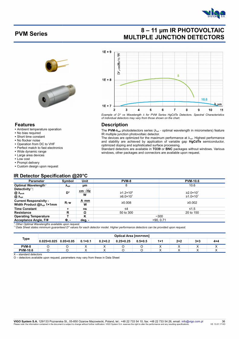
PVM Series8 – 11 μm IR PHOTOVOLTAIC
MULTIPLE JUNCTION DETECTORS
Example of D* vs Wavelength λ for PVM Series HgCdTe Detectors. Spectral Characteristicsof individual detectors may vary from those shown on the chart.
Features• Ambient temperature operation• No bias required• Short time constant• No flocker noise• Operation from DC to VHF• Perfect match to fast electronics• Wide dynamic range• Large area devices• Low cost• Prompt delivery• Custom design upon request
DescriptionThe PVM-λopt photodetectors series (λopt - optimal wavelength in micrometers) featureIR multiple junction photovoltaic detector.The devices are optimized for the maximum performance at λopt. Highest performanceand stability are achieved by application of variable gap HgCdTe semiconductor,optimized doping and sophisticated surface processing.Standard detectors are available in TO39 or BNC packages without windows. Variouswindows, other packages and connectors are available upon request.
IR Detector Specification @20°CParameter Symbol Unit PVM-8 PVM-10.6
Optimal Wavelength*) λopt µm 8 10.6Detectivity**):@ λpeak
@ λopt
D*cm⋅√Hz
W≥1.2×10⁸
≥6.0×10⁷≥2.0×10⁷
≥1.0×10⁷
Current Responsivity - Width Product @λopt 1×1mm
Ri·wA⋅mm
W≥0.008 ≥0.002
Time Constant τ ns ≤4 ≤1.5Resistance R Ω 50 to 300 20 to 150Operating Temperature T K ~300Acceptance Angle, F/# Φ, - deg, - >90, 0.71
*) Other Optimal Wavelengths available upon request.**) Data Sheet states minimum guaranteed D* values for each detector model. Higher performance detectors can be provided upon request.
TypeOptical Area [mm×mm]
0.025×0.025 0.05×0.05 0.1×0.1 0.2×0.2 0.25×0.25 0.5×0.5 1×1 2×2 3×3 4×4
PVM-8 O O X X O O X X X XPVM-10.6 O O X X O O X X X X
X – standard detectorsO – detectors available upon request, parameters may vary from these in Data Sheet
VIGO System S.A. 129/133 Poznanska St., 05-850 Ozarow Mazowiecki, Poland, tel.: +48 22 733 54 10, fax: +48 22 733 54 26, email: [email protected] 36Please note: the information contained in the document is subject to change without further notification. VIGO System S.A. reserves the right to alter the performance and any resulting specifications. VS 13.01.17 KO

PVM-2TE Series8 – 11 μm IR PHOTOVOLTAIC
MULTIPLE JUNCTION DETECTORSTHERMOELECTRICALLY COOLED
Example of D* vs Wavelength λ for PVM-2TE Series HgCdTe Detectors. Spectral Characteristicsof individual detectors may vary from those shown on the chart.
Features• High performance in the 8 to 11 µm spectral range• Fast response• No flicker noise• Convenient to use• Wide dynamic range• Compact, rugged and reliable• Low cost• Prompt delivery• Custom design upon request
DescriptionThe PVM-2TE-λopt photodetectors series (λopt - optimal wavelength in micrometers)feature IR multiple junction photovoltaic detector on two-stage thermoelectrical cooler.The devices are optimized for the maximum performance at λopt, large area devices.Highest performance and stability are achieved by application of variable gap HgCdTesemiconductor, optimized doping and sophisticated surface processing. Customdevices with quadrant cells, multielement arrays, different windows, lenses and opticalfilters are available upon request.Standard detectors are available in TO8 packages with wZnSeAR windows. Otherpackages, windows and connectors are also available.
IR Detector Specification @20°CParameter Symbol Unit PVM-2TE-8 PVM-2TE-10.6
Optimal Wavelength*) λopt µm 8 10.6Detectivity**):@ λpeak
@ λopt
D*cm⋅√Hz
W≥6.0×10⁸
≥3.0×10⁸≥2.0×10⁸
≥1.0×10⁸
Current Responsivity - Width Product @λopt 1×1mm
Ri·wA⋅mm
W≥0.015 ≥0.006
Time Constant τ ns ≤4 ≤3Resistance R Ω 150 to 600 100 to 350Operating Temperature T K ~230Acceptance Angle, F/# Φ, - deg, - 70, 0.87
*) Other Optimal Wavelengths available upon request.**) Data Sheet states minimum guaranteed D* values for each detector model. Higher performance detectors can be provided upon request.
TypeOptical Area [mm×mm]
0.025×0.025 0.05×0.05 0.1×0.1 0.2×0.2 0.25×0.25 0.5×0.5 1×1 2×2 3×3 4×4
PVM-2TE-8 O O X X O O X X XPVM-2TE-10.6 O O X X O O X X X
X – standard detectorsO – detectors available upon request, parameters may vary from these in Data Sheet
VIGO System S.A. 129/133 Poznanska St., 05-850 Ozarow Mazowiecki, Poland, tel.: +48 22 733 54 10, fax: +48 22 733 54 26, email: [email protected] 37Please note: the information contained in the document is subject to change without further notification. VIGO System S.A. reserves the right to alter the performance and any resulting specifications. VS 13.01.17 KO

PVMI Series8 – 11 μm IR PHOTOVOLTAIC
MULTIPLE JUNCTION DETECTORSOPTICALLY IMMERSED
Example of D* vs Wavelength λ for PVMI Series HgCdTe Detectors. Spectral Characteristicsof individual detectors may vary from those shown on the chart.
Features• Ambient temperature operation• No bias required• Short time constant• No flocker noise• Operation from DC to VHF• Perfect match to fast electronics• Wide dynamic range• Low cost• Custom design upon request
DescriptionThe PVMI-λopt photodetectors series (λopt - optimal wavelength in micrometers) featureIR multiple junction optically immersed photovoltaic detector.The devices are optimized for the maximum performance at λopt. Highest performanceand stability are achieved by application of variable gap HgCdTe semiconductor,optimized doping and sophisticated surface processing.Standard detectors are available in TO39 or BNC packages without windows. Variouswindows, other packages and connectors are available upon request.
IR Detector Specification @20°CParameter Symbol Unit PVMI-8 PVMI-10.6
Optimal Wavelength*) λopt µm 8 10.6Detectivity**):@ λpeak
@ λopt
D*cm⋅√Hz
W≥6.0×10⁸
≥3.0×10⁸≥2.0×10⁸
≥1.0×10⁸
Current Responsivity - Width Product @λopt 1×1mm
Ri·wA⋅mm
W≥0.04 ≥0.01
Time Constant τ ns ≤4 ≤1.5Resistance R Ω 50 to 300 20 to 150Operating Temperature T K ~300Acceptance Angle, F/# Φ, - deg, - 36, 1.62
*) Other Optimal Wavelengths available upon request.**) Data Sheet states minimum guaranteed D* values for each detector model. Higher performance detectors can be provided upon request.
TypeOptical Area [mm×mm]
0.025×0.025 0.05×0.05 0.1×0.1 0.2×0.2 0.25×0.25 0.5×0.5 1×1 2×2 3×3 4×4
PVMI-8 O O X XPVMI-10.6 O O X X
X – standard detectorsO – detectors available upon request, parameters may vary from these in Data Sheet
VIGO System S.A. 129/133 Poznanska St., 05-850 Ozarow Mazowiecki, Poland, tel.: +48 22 733 54 10, fax: +48 22 733 54 26, email: [email protected] 38Please note: the information contained in the document is subject to change without further notification. VIGO System S.A. reserves the right to alter the performance and any resulting specifications. VS 13.01.17 KO

PVMI-2TE Series
8 – 11 μm IR PHOTOVOLTAICMULTIPLE JUNCTION DETECTORSTHERMOELECTRICALLY COOLED
OPTICALLY IMMERSED
Example of D* vs Wavelength λ for PVMI-2TE Series HgCdTe Detectors. Spectral Characteristicsof individual detectors may vary from those shown on the chart.
Features• High performance in the long wavelengths range without
LN cooling• Fast response• No flicker noise• Convenient to use• Wide dynamic range• Compact, rugged and reliable• Low cost• Prompt delivery• Custom design upon request
DescriptionThe PVMI-2TE-λopt photodetectors series (λopt - optimal wavelength in micrometers)feature IR multiple junction optically immersed photovoltaic detectors on two-stagethermoelectrical cooler.The devices are optimized for the maximum performance at λopt. Highest performanceand stability are achieved by application of variable gap HgCdTe semiconductor,optimized doping and sophisticated surface processing. Custom devices with quadrantcells, multielement arrays, different windows, lenses and optical filters are availableupon request.Standard detectors are available in TO8 packages with wZnSeAR windows. Otherpackages, windows and connectors are also available.
IR Detector Specification @20°CParameter Symbol Unit PVMI-2TE-8 PVMI-2TE-10.6
Optimal Wavelength*) λopt µm 8 10.6Detectivity**):@ λpeak
@ λopt
D*cm⋅√Hz
W≥2.5×10⁹
≥2.0×10⁹≥1.5×10⁹
≥1.0×10⁹
Current Responsivity - Width Product @λopt 1×1mm
Ri·wA⋅mm
W≥0.10 ≥0.05
Time Constant τ ns ≤4 ≤3Resistance R Ω 150 to 600 100 to 350Operating Temperature T K ~230Acceptance Angle, F/# Φ, - deg, - 36, 1.62
*) Other Optimal Wavelengths available upon request.**) Data Sheet states minimum guaranteed D* values for each detector model. Higher performance detectors can be provided upon request.
TypeOptical Area [mm×mm]
0.025×0.025 0.05×0.05 0.1×0.1 0.2×0.2 0.25×0.25 0.5×0.5 1×1 2×2 3×3 4×4
PVMI-2TE-8 O O X XPVMI-2TE-10.6 O O X X
X – standard detectorsO – detectors available upon request, parameters may vary from these in Data Sheet
VIGO System S.A. 129/133 Poznanska St., 05-850 Ozarow Mazowiecki, Poland, tel.: +48 22 733 54 10, fax: +48 22 733 54 26, email: [email protected] 39Please note: the information contained in the document is subject to change without further notification. VIGO System S.A. reserves the right to alter the performance and any resulting specifications. VS 13.01.17 KO

PVMI-3TE Series
8 – 11 μm IR PHOTOVOLTAICMULTIPLE JUNCTION DETECTORSTHERMOELECTRICALLY COOLED
OPTICALLY IMMERSED
Example of D* vs Wavelength λ for PVMI-3TE Series HgCdTe Detectors. Spectral Characteristicsof individual detectors may vary from those shown on the chart.
Features• High performance in the long wavelengths range without
LN cooling• Fast response• No flicker noise• Convenient to use• Wide dynamic range• Compact, rugged and reliable• Low cost• Prompt delivery• Custom design upon request
DescriptionThe PVMI-3TE-λopt photodetectors series (λopt - optimal wavelength in micrometers)feature IR multiple junction optically immersed photovoltaic detectors on three-stagethermoelectrical cooler.The devices are optimized for the maximum performance at λopt. Highest performanceand stability are achieved by application of variable gap HgCdTe semiconductor,optimized doping and sophisticated surface processing. Custom devices with quadrantcells, multielement arrays, different windows, lenses and optical filters are availableupon request.Standard detectors are available in TO8 packages with wZnSeAR windows. Otherpackages, windows and connectors are also available.
IR Detector Specification @20°CParameter Symbol Unit PVMI-3TE-8 PVMI-3TE-10.6
Optimal Wavelength*) λopt µm 8 10.6Detectivity**):@ λpeak
@ λopt
D*cm⋅√Hz
W≥4.0×10⁹
≥3.0×10⁹≥2.0×10⁹
≥1.5×10⁹
Current Responsivity - Width Product @λopt 1×1mm
Ri·wA⋅mm
W≥0.15 ≥0.10
Time Constant τ ns ≤4 ≤3Resistance R Ω 200 to 1200 100 to 400Operating Temperature T K ~210Acceptance Angle, F/# Φ, - deg, - 36, 1.62
*) Other Optimal Wavelengths available upon request.**) Data Sheet states minimum guaranteed D* values for each detector model. Higher performance detectors can be provided upon request.
TypeOptical Area [mm×mm]
0.025×0.025 0.05×0.05 0.1×0.1 0.2×0.2 0.25×0.25 0.5×0.5 1×1 2×2 3×3 4×4
PVMI-3TE-8 O O X XPVMI-3TE-10.6 O O X X
X – standard detectorsO – detectors available upon request, parameters may vary from these in Data Sheet
VIGO System S.A. 129/133 Poznanska St., 05-850 Ozarow Mazowiecki, Poland, tel.: +48 22 733 54 10, fax: +48 22 733 54 26, email: [email protected] 40Please note: the information contained in the document is subject to change without further notification. VIGO System S.A. reserves the right to alter the performance and any resulting specifications. VS 13.01.17 KO

PVMI-4TE Series
8 – 11 μm IR PHOTOVOLTAICMULTIPLE JUNCTION DETECTORSTHERMOELECTRICALLY COOLED
OPTICALLY IMMERSED
Example of D* vs Wavelength λ for PVMI-4TE Series HgCdTe Detectors. Spectral Characteristicsof individual detectors may vary from those shown on the chart.
Features• High performance in the long wavelengths range without
LN cooling• Fast response• No flicker noise• Convenient to use• Wide dynamic range• Compact, rugged and reliable• Low cost• Prompt delivery• Custom design upon request
DescriptionThe PVMI-4TE-λopt photodetectors series (λopt - optimal wavelength in micrometers)feature IR multiple junction optically immersed photovoltaic detectors on four-stagethermoelectrical cooler.The devices are optimized for the maximum performance at λopt. Highest performanceand stability are achieved by application of variable gap HgCdTe semiconductor,optimized doping and sophisticated surface processing. Custom devices with quadrantcells, multielement arrays, different windows, lenses and optical filters are availableupon request.Standard detectors are available in TO8 packages with wZnSeAR windows. Otherpackages, windows and connectors are also available.
IR Detector Specification @20°CParameter Symbol Unit PVMI-4TE-8 PVMI-4TE-10.6
Optimal Wavelength*) λopt µm 8 10.6Detectivity**):@ λpeak
@ λopt
D*cm⋅√Hz
W≥8.0×10⁹
≥6.0×10⁹≥2.5×10⁹
≥2.0×10⁹
Current Responsivity - Width Product @λopt 1×1mm
Ri·wA⋅mm
W≥0.20 ≥0.15
Time Constant τ ns ≤4 ≤3Resistance R Ω 500 to 1200 150 to 500Operating Temperature T K ~195Acceptance Angle, F/# Φ, - deg, - 36, 1.62
*) Other Optimal Wavelengths available upon request.**) Data Sheet states minimum guaranteed D* values for each detector model. Higher performance detectors can be provided upon request.
TypeOptical Area [mm×mm]
0.025×0.025 0.05×0.05 0.1×0.1 0.2×0.2 0.25×0.25 0.5×0.5 1×1 2×2 3×3 4×4
PVMI-4TE-8 O O X XPVMI-4TE-10.6 O O X X
X – standard detectorsO – detectors available upon request, parameters may vary from these in Data Sheet
VIGO System S.A. 129/133 Poznanska St., 05-850 Ozarow Mazowiecki, Poland, tel.: +48 22 733 54 10, fax: +48 22 733 54 26, email: [email protected] 41Please note: the information contained in the document is subject to change without further notification. VIGO System S.A. reserves the right to alter the performance and any resulting specifications. VS 13.01.17 KO

INFRARED DETECTORSACCESSORIES
VIGO System S.A. 129/133 Poznanska St., 05-850 Ozarow Mazowiecki, Poland, tel.: +48 22 733 54 10, fax: +48 22 733 54 26, email: [email protected] 42Please note: the information contained in the document is subject to change without further notification. VIGO System S.A. reserves the right to alter the performance and any resulting specifications. VS 13.01.17 KO

Preamplifier Series
VIP FIP BIP MIP PIP SIP QIP
Application standalone fast OEM STANDARDSTANDARD
programmableultra small four channel
Size large medium medium medium medium small mediumSpeed slow fast medium medium medium medium mediumIntegrated Detector ✘ ✔ ✔ ✔ ✔ ✔ ✔Cooled / Uncooled Detector ✘ /✔ ✔/✔ ✔/✔ ✔/✔ ✔/✔ ✔/✔ ✘ /✔4 channel ✘ ✘ ✘ ✘ ✘ ✘ ✔Tuned Gain ✘ ✘ ✘ ✘ ✔ option optionProgrammable Gain ✘ ✘ ✘ ✘ ✔ ✘ ✘Programmable Bandwidth ✘ ✘ ✘ ✘ ✔ ✘ ✘Additonal DC Output ✘ option on request on request ✘ ✘ ✘Page 44 47 51 55 59 63 67
TEC ControllersSTCC-04 ✘ ✔ ✔ ✔ ✘ ✔ ✘MTCC-01 ✘ ✔ ✔ ✔ ✘ ✔ ✘PTCC-01 ✘ ✔ ✔ ✔ ✔ ✔ ✘
Power SuppliesPPS-02 ✔ ✘ ✘ ✘ ✘ ✔ ✔PPS-03 ✔ ✘ ✘ ✘ ✘ ✔ ✔MPPS-01 ✔ ✔ ✔ ✔ ✘ ✔ ✔
CablesBNC-BNC ✔ ✘ ✘ ✘ ✘ ✘ ✘SMA-BNC ✘ ✔ ✔ ✔ ✔ ✘ ✘SMA-SMA ✘ ✔ ✔ ✔ ✔ ✘ ✘MMCX-BNC ✘ ✘ ✘ ✘ ✘ ✔ ✘MMCX-SMA ✘ ✘ ✘ ✘ ✘ ✔ ✘MCX-BNC ✘ ✘ ✘ ✘ ✘ ✘ ✔MCX-SMA ✘ ✘ ✘ ✘ ✘ ✘ ✔AMP2x4-DB9 ✘ ✘ ✔ ✘ ✘ ✔ ✔AMP2x4-DUBOX2x5 ✘ ✘ ✔ ✘ ✘ ✔ ✘AMP2x4-AMP2x4 ✘ ✘ ✔ ✘ ✘ ✔ ✘LEMO-DB9 ✘ ✔ ✘ ✔ ✔ ✘ ✘LEMO-DUBOX2x5 ✘ ✔ ✘ ✔ ✔ ✘ ✘LEMO-AMP2X4 ✘ ✔ ✘ ✔ ✘ ✘ ✘AMP1x6-MIC5 ✘ ✔ ✔ ✔ ✘ ✔ ✘AMP1x6-POWER ✘ ✔ ✔ ✔ ✘ ✔ ✘DB9-DB9 ✔ ✘ ✘ ✘ ✘ ✘ ✘DB9-4mmPLUGS ✔ ✘ ✘ ✘ ✘ ✘ ✘DB9-MIC5 ✔ ✘ ✘ ✘ ✘ ✘ ✘AMP2x4-MIC5 ✘ ✘ ✘ ✘ ✘ ✔ ✔KK2-POWER ✘ ✔ ✔ ✔ ✔ ✔ ✘USB:TypeA-MicroB ✘ ✔ ✔ ✔ ✔ ✔ ✘Power Cable EU ✔ ✔ ✔ ✔ ✘ ✔ ✘Power Cable UK ✔ ✔ ✔ ✔ ✘ ✔ ✘Power Cable US ✔ ✔ ✔ ✔ ✘ ✔ ✘
AC AdaptorsAC Adaptor ✔ ✔ ✔ ✔ ✔ ✔ ✔
Mechanical AccessoriesDRB-1 ✔ ✔ ✘ ✔ ✔ ✘ ✔DRB-2 ✔ ✔ ✘ ✔ ✔ ✘ ✔MP ✔ ✔ ✘ ✔ ✔ ✘ ✔PH ✔ ✔ ✘ ✔ ✔ ✘ ✔BP ✔ ✔ ✘ ✔ ✔ ✘ ✔STA-8x1-4 ✔ ✔ ✘ ✔ ✔ ✘ ✔MHS-1 ✘ ✘ ✔ ✘ ✘ ✘ ✘MHS-2 ✘ ✘ ✘ ✘ ✘ ✔ ✘MHS-3 ✘ ✘ ✘ ✘ ✘ ✘ ✔DH-BNC-1 ✔ ✘ ✘ ✘ ✘ ✘ ✘DH-BNC-2 ✔ ✘ ✘ ✘ ✘ ✘ ✘EL-1 ✘ ✘ ✘ ✔ ✔ ✘ ✘
VIGO System S.A. 129/133 Poznanska St., 05-850 Ozarow Mazowiecki, Poland, tel.: +48 22 733 54 10, fax: +48 22 733 54 26, email: [email protected] 43Please note: the information contained in the document is subject to change without further notification. VIGO System S.A. reserves the right to alter the performance and any resulting specifications. VS 13.01.17 KO
VIP Series STANDALONE PREAMPLIFIER
Features• Compact size• High signal-to-noise ratio• Bandwidth up to 20 MHz• Dedicated to operate with uncooled detector in BNC package• Custom configurations upon request• Additional accessories available
Applications• Contactless temperature measurement• Laser radiation detection• Gas analysis• Fourier spectroscopy• Fire, flame and human body detection• Pyrometers, scanners • Nondestructive material testing
DescriptionVIP is the transimpedance, AC or DC coupled, standalone preamplifier.It is dedicated for operation with uncooled, no biasing IR detectors inBNC packages.
Preamplifier Specification
Parameter Symbol Unit Typical Value Conditions, Remarks
Input Noise Voltage Density ennV√Hz
0.97 – 8.01) fo = 100 kHz2)
Input Noise Current Density inpA√Hz
0.02 – 3.51) fo = 100 kHz2)
Low Cut-Off Frequency flo HzDC
10 to 10kDC coupling setAC coupling set
High Cut-Off Frequency fhi Hz 100k to 20M
Transimpedance KiVA
up to 1×10⁵
Output Impedance Rout Ω 50
Output Voltage Swing Vout V±10±2±1
fhi ≤ 1 MHz,1 MHz < fhi ≤ 20 MHz,
20 MHz < fhi ≤ 250 MHz,
RL = 1 MΩ3)
RL = 1 MΩ3)
RL = 50 Ω3)
Output Voltage Offset Voff mV ≤20 DC and AC coupling set
Power Supply Voltage Vsup V±15±9
fhi ≤ 1 MHz1 MHz < fhi ≤ 20 MHz
Power Supply Current Isup mA ±25
Dimensions - mm×mm×mm 50×104×23.5 width×depth×height
Weight - g 260
Electrical characteristics @ Ta = 20 °C.
1) The preamplifier noise may significantly reduce the system performance in some situations. This happens for large capacitance detectors operating at high frequencies.2) f0 – noise measurement frequency3) RL – load resistance
VIGO System S.A. 129/133 Poznanska St., 05-850 Ozarow Mazowiecki, Poland, tel.: +48 22 733 54 10, fax: +48 22 733 54 26, email: [email protected] 44Please note: the information contained in the document is subject to change without further notification. VIGO System S.A. reserves the right to alter the performance and any resulting specifications. VS 13.01.17 KO

VIP Series
Preamplifier Code Description
VIP-flo-fhi-P1
The preamplifier can be integrated with followingtypes IR detectors:
Detector Type Description
PV photovoltaic
PVI photovoltaic, optically immersed
PVM multiple heterojunction photovoltaic
PVMImultiple heterojunction photovoltaic,
optically immersed
Schematic Diagram
Power Supply Connector
Pin Number Symbol Function
1 N.C. not connected
2 N.C. not connected
3 GND power ground
4 N.C. not connected
5 N.C. not connected
6 –Vsup power supply input (–)
7 N.C. not connected
8 N.C. not connected
9 +Vsup power supply input (+)
DB9 Connector Male
Physical Dimensions [mm]
VIGO System S.A. 129/133 Poznanska St. 05-850 Ozarow Mazowiecki, Poland, tel.: +48 22 733 54 10, fax: +48 22 733 54 26, email: [email protected] 45Please note: the information contained in the document is subject to change without further notification. VIGO System S.A. reserves the right to alter the performance and any resulting specifications. VS 13.01.17 KO
From Detector Unit
SupplyRegulator
TransimpedancePreamplifier
VoltageAmplifier
EMIFilters
DB9Supply Connector
BNCOutput Connector
1 2 3 4 5
6 7 8 9
P1 – supply connector: S – standard H – pigtail cable
fhi – high cut-off frequency in Hz:
100k, 300k, 1M, 5M, 10M, 20M
flo – low cut-off frequency in Hz:
DC, 10, 100, 1k, 10k
VIP – preamplifier series V – Version, I – Current Input, P – Preamplifier

VIP Series
Recommended Accessories
PPS-02 PPS-03 MPPS-01 BNC-BNC DB9-DB9
Preamplifier Power Supply Preamplifier Power Supply Preamplifier Power Supply Signal Input or Output Cable Preamplifier Supply Cable
DB9-4mmPLUGS DB9-MIC5 AC Adaptor Power Cable EU Power Cable UK
Preamplifier Supply Cable Preamplifier Supply Cable Power Supply Adaptor Power Cable Power Cable
Power Cable US DRB-1 DRB-2 MP PH
Power Cable Base Mounting System Base Mounting System Mounting Post Post Holder
STA-8x1-4 DH-BNC-1
Special Thread Adapter Detector's Holder
VIGO System S.A. 129/133 Poznanska St. 05-850 Ozarow Mazowiecki, Poland, tel.: +48 22 733 54 10, fax: +48 22 733 54 26, email: [email protected] 46Please note: the information contained in the document is subject to change without further notification. VIGO System S.A. reserves the right to alter the performance and any resulting specifications. VS 13.01.17 KO

FIP Series FAST PREAMPLIFIER
Features• Compact size• Wide bandwidth up to 1GHz• Precise I-V conversion• Detector biasing possibility up to +800 mV• Low current noise• Co-operation with high-resistance detectors• Effective cooling up to 4-stage TE coolers
Applications• Laser technology• Fast laser pulse measurements• Telemetry• Sighting systems• Free space optics
DescriptionFIP is the high speed transimpedance, AC coupled preamplifier. It isdedicated for high speed infrared measurements.FIP preamplifier is designed for operation with either biased or non-biased TE cooled detectors.
Preamplifier Specification
Parameter Symbol Unit Typical Value Conditions, Remarks
Input Noise Voltage Density ennV√Hz
1.11) fo = 100 kHz2)
Input Noise Current Density inpA√Hz
51) fo = 100 kHz2)
Low Cut-Off Frequency flo Hz 1k, 10k 3 dB
High Cut-Off Frequency fhi Hz 1G 3 dB
Transimpedance KiVA
8.5×10³
Output Impedance Rout Ω 50
Output Voltage Swing Vout V ±0.8 RL = 50 Ω3)
Power Supply Voltage Vsup V+12-5
Power Supply Current Isup mA+100-50
no detector biasing
Dimensions - mm×mm×mm45×89.5×48.545×91×48.5
45×92.5×48.5
width×depth×height - with 2TEwidth×depth×height - with 3TEwidth×depth×height - with 4TE
Electrical characteristics @ Ta = 20 °C.
1) The preamplifier noise may significantly reduce the system performance in some situations. This happens for large capacitance detectors operating at high frequencies.2) f0 – noise measurement frequency3) RL – load resistance
VIGO System S.A. 129/133 Poznanska St., 05-850 Ozarow Mazowiecki, Poland, tel.: +48 22 733 54 10, fax: +48 22 733 54 26, email: [email protected] 47Please note: the information contained in the document is subject to change without further notification. VIGO System S.A. reserves the right to alter the performance and any resulting specifications. VS 13.01.17 KO

FIP Series
Preamplifier Code Description
FIP-flo-fhi-P1-P2-P3
The preamplifier can be integrated with followingtypes IR detectors:
Detector Type Description
PC-2TE, PC-3TE, PC-4TE photoconductive
PCI, PCI-2TE, PCI-3TE,PCI-4TE
photoconductive,optically immersed
PV-2TE, PV-3TE, PV-4TE photovoltaic
PVI-2TE, PVI-3TE, PVI-4TEphotovoltaic,
optically immersed
PVM-2TE, PVM-3TE, PVM-4TEmultiple heterojunction
photovoltaic
PVMI-2TE, PVMI-3TE,PVMI-4TE
multiple heterojunctionphotovoltaic,
optically immersed
Symbol -2TE, -3TE, -4TE means 2, 3 or 4-stage TEC integrated with detector.
Schematic Diagram
Power Supply and TEC Control Connector
Pin number Symbol Function
1 FAN+ FAN (+)
2 TH2 thermistor output (2)
3 TEC– TEC supply input (–)
4 –Vsup power supply input (–)
5 GND power ground
6 +Vsup power supply input (+)
7 TEC+ TEC supply input (+)
8 TH1 thermistor output (1)
9 DATA data pin
LEMO Connector Female
VIGO System S.A. 129/133 Poznanska St., 05-850 Ozarow Mazowiecki, Poland, tel.: +48 22 733 54 10, fax: +48 22 733 54 26, email: [email protected] 48Please note: the information contained in the document is subject to change without further notification. VIGO System S.A. reserves the right to alter the performance and any resulting specifications. VS 13.01.17 KO
Detector Unit
IR Sensitive Area
Thermistor1)
TE-Cooler1)
DetectorBiasing2)
SupplyRegulator
TransimpedancePreamplifier
VoltageAmplifier
EMIFilters
LEMOSupply & Control
Connector
SMA OutputConnector
1), Only for TE-cooled detectors2) Only for biased detectors
ConfigurationMemory
DATA
1
7 3
5
28
46
9
P3 – additional DC output: D – with output ND – no DC output
P2 – mounting hole: M4 – M4 mounting hole M8 – M8x1 mounting hole
P1 – package: F – with fan
fhi – high cut-off frequency in Hz:
1G
flo – low cut-off frequency in Hz:
available options: 1k,10k
FIP – preamplifier series F – Version, I – Current Input, P – Preamplifier

FIP Series
Physical Dimensions [mm]
VIGO System S.A. 129/133 Poznanska St., 05-850 Ozarow Mazowiecki, Poland, tel.: +48 22 733 54 10, fax: +48 22 733 54 26, email: [email protected] 49Please note: the information contained in the document is subject to change without further notification. VIGO System S.A. reserves the right to alter the performance and any resulting specifications. VS 13.01.17 KO

FIP Series
Recommended Accessories
PTCC-01-OEM PTCC-01-BAS PTCC-01-ADV STCC-04 MTCC-01
Programmable “Smart” TECController – OEM
Programmable “Smart” TECController – Basic
Programmable “Smart” TECController – Advanced
Standard TEC Controller Miniature TEC Controller
MPPS-01 SMA-BNC SMA-SMA LEMO-DB9 LEMO-DUBOX2x5
Preamplifier Power Supply Signal Output Cable Signal Output Cable TEC and Supply Cable TEC and Supply Cable
LEMO-AMP2x4 AMP1x6-MIC5 AMP1x6-POWER KK2-POWER USB: TypeA-MicroB
TEC and Supply Cable Power Supply Cable Power Supply Cable Power Supply Cable Cable for PC Connection
AC Adaptor Power Cable EU Power Cable UK Power Cable US DRB-1
Power Supply Adaptor Power Cable Power Cable Power Cable Base Mounting System
DRB-2 MP PH STA-8x1-4
Base Mounting System Mounting Post Post Holder Special Thread Adapter
VIGO System S.A. 129/133 Poznanska St., 05-850 Ozarow Mazowiecki, Poland, tel.: +48 22 733 54 10, fax: +48 22 733 54 26, email: [email protected] 50Please note: the information contained in the document is subject to change without further notification. VIGO System S.A. reserves the right to alter the performance and any resulting specifications. VS 13.01.17 KO

BIP Series OEM PREAMPLIFIER
Features• Compact size• High signal-to-noise ratio• Bandwidth up to 250 MHz• Dedicated to operate with 2-, 3- and 4-stage TE cooled detectors• Custom modifications upon request• Additional accessories available
Applications• Contactless temperature measurement• Free space optical communication• Laser radiation detection• Gas analysis• Fourier spectroscopy• Fire, flame and human body detection• Pyrometers, scanners• Nondestructive material testing• OEM applicationsDescription
BIP is the transimpedance, AC or DC coupled preamplifier. It isdedicated for OEM applications and requires external heat sink (seeRecommended Accessories).BIP preamplifier is designed for operation with either biased ornon-biased TE cooled detectors.
Preamplifier Specification
Parameter Symbol Unit Typical Value Conditions, Remarks
Input Noise Voltage Density ennV
√Hz0.97 – 8.01) fo = 10 kHz2)
Input Noise Current Density inpA
√Hz0.02 – 3.51) fo = 10 kHz2)
Low Cut-Off Frequency flo HzDC
10 to 10kDC coupling setAC coupling set
High Cut-Off Frequency fhi Hz 100k to 250M
Transimpedance KiVA
up to 2×10⁵
Output Impedance Rout Ω 50
Output Voltage Swing Vout V±10±2±1
fhi ≤ 1 MHz,1 MHz < fhi ≤ 20 MHz,
20 MHz < fhi ≤ 250 MHz,
RL = 1 MΩ3)
RL = 1 MΩ3)
RL = 50 Ω3)
Output Voltage Offset Voff mV max ±204)
Power Supply Voltage Vsup V±15±9
fhi ≤ 1 MHzfhi > 1 MHz
Power Supply Current Isup mA max ±50 no detector biasing
Dimensions - mm×mm×mm 45×80.5×25 width×depth×height - with 2TE, 3TE, 4TE
Electrical characteristics @ Ta = 20 °C.
1) The preamplifier noise may significantly reduce the system performance in some situations. This happens for large capacitance detectors operating at high frequencies.2) f0 – noise measurement frequency3) RL – load resistance4) Measured with equivalent resistor at the input instead of the detector. It's to avoid the environmental thermal radiation's impact.
VIGO System S.A. 129/133 Poznanska St., 05-850 Ozarow Mazowiecki, Poland, tel.: +48 22 733 54 10, fax: +48 22 733 54 26, email: [email protected] 51Please note: the information contained in the document is subject to change without further notification. VIGO System S.A. reserves the right to alter the performance and any resulting specifications. VS 13.01.17 KO
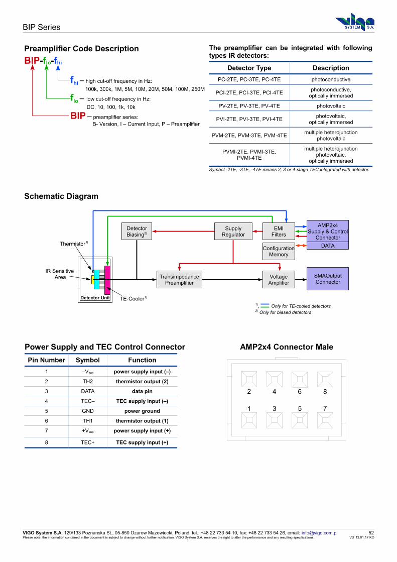
BIP Series
Preamplifier Code Description
BIP-flo-fhi
The preamplifier can be integrated with followingtypes IR detectors:
Detector Type Description
PC-2TE, PC-3TE, PC-4TE photoconductive
PCI-2TE, PCI-3TE, PCI-4TEphotoconductive,
optically immersed
PV-2TE, PV-3TE, PV-4TE photovoltaic
PVI-2TE, PVI-3TE, PVI-4TEphotovoltaic,
optically immersed
PVM-2TE, PVM-3TE, PVM-4TEmultiple heterojunction
photovoltaic
PVMI-2TE, PVMI-3TE,PVMI-4TE
multiple heterojunctionphotovoltaic,
optically immersed
Symbol -2TE, -3TE, -4TE means 2, 3 or 4-stage TEC integrated with detector.
Schematic Diagram
Power Supply and TEC Control Connector
Pin Number Symbol Function
1 –Vsup power supply input (–)
2 TH2 thermistor output (2)
3 DATA data pin
4 TEC– TEC supply input (–)
5 GND power ground
6 TH1 thermistor output (1)
7 +Vsup power supply input (+)
8 TEC+ TEC supply input (+)
AMP2x4 Connector Male
VIGO System S.A. 129/133 Poznanska St., 05-850 Ozarow Mazowiecki, Poland, tel.: +48 22 733 54 10, fax: +48 22 733 54 26, email: [email protected] 52Please note: the information contained in the document is subject to change without further notification. VIGO System S.A. reserves the right to alter the performance and any resulting specifications. VS 13.01.17 KO
Detector Unit
IR Sensitive Area
Thermistor1)
TE-Cooler1)
DetectorBiasing2)
SupplyRegulator
TransimpedancePreamplifier
VoltageAmplifier
EMIFilters
AMP2x4Supply & Control
Connector
SMAOutputConnector
1), Only for TE-cooled detectors2) Only for biased detectors
ConfigurationMemory
DATA
2 4 6 8
7531
fhi – high cut-off frequency in Hz:
100k, 300k, 1M, 5M, 10M, 20M, 50M, 100M, 250M
flo – low cut-off frequency in Hz:
DC, 10, 100, 1k, 10k
BIP – preamplifier series: B- Version, I – Current Input, P – Preamplifier
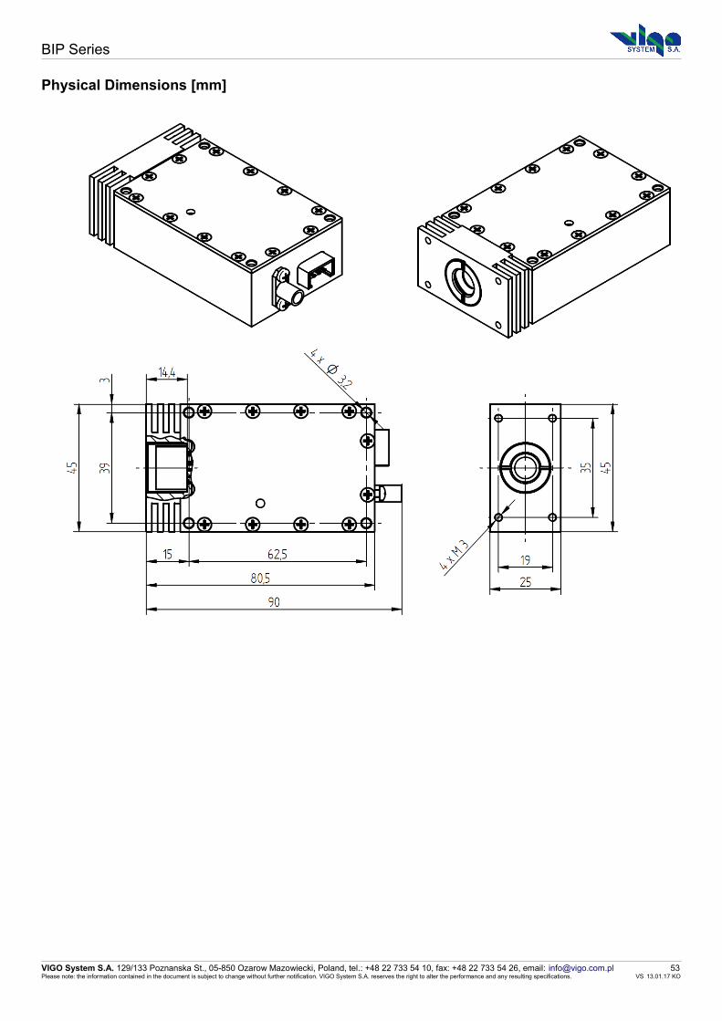
BIP Series
Physical Dimensions [mm]
VIGO System S.A. 129/133 Poznanska St., 05-850 Ozarow Mazowiecki, Poland, tel.: +48 22 733 54 10, fax: +48 22 733 54 26, email: [email protected] 53Please note: the information contained in the document is subject to change without further notification. VIGO System S.A. reserves the right to alter the performance and any resulting specifications. VS 13.01.17 KO

BIP Series
Recommended Accessories
PTCC-01-OEM PTCC-01-BAS PTCC-01-ADV STCC-04 MTCC-01
Programmable “Smart” TECController – OEM
Programmable “Smart” TECController – Basic
Programmable “Smart” TECController – Advanced
Standard TEC Controller Miniature TEC Controller
MPPS-01 SMA-BNC SMA-SMA AMP2x4-DB9 AMP2x4-DUBOX2x5
Preamplifier Power Supply Signal Output Cable Signal Output Cable TEC and Supply Cable TEC and Supply Cable
AMP2x4-AMP2x4 AMP1x6-MIC5 AMP1x6-POWER KK2-POWER USB: TypeA-MicroB
TEC and Supply Cable Power Supply Cable Power Supply Cable Power Supply Cable Cable for PC Connection
AC Adaptor Power Cable EU Power Cable UK Power Cable US MHS-1
Power Supply Adaptor Power Cable Power Cable Power Cable Additional Heat Sink
VIGO System S.A. 129/133 Poznanska St., 05-850 Ozarow Mazowiecki, Poland, tel.: +48 22 733 54 10, fax: +48 22 733 54 26, email: [email protected] 54Please note: the information contained in the document is subject to change without further notification. VIGO System S.A. reserves the right to alter the performance and any resulting specifications. VS 13.01.17 KO

MIP Series MEDIUM SIZE PREAMPLIFIER
Features• Compact size• High signal-to-noise ratio• Bandwidth up to 250 MHz• Dedicated for operation with 2-, 3- and 4-stage TE cooled detectors• Custom configuration upon request• Additional accessories available
Applications• Contactless temperature measurement• Free space optical communication• Laser radiation detection• Gas analysis• Fourier spectroscopy• Fire, flame and human body detection• Pyrometers, scanners• Nondestructive material testing• OEM applications
DescriptionMIP is the transimpedance, AC or DC coupled preamplifier. It isdedicated for BenchTop applications. Package type F is equipped withfan and does not require additonal heat sink. Pacakage type NF requiresadditional heat dissipation (provided by user).MIP preamplifier is designed for operation with either biased or non-biased cooled detectors.
Preamplifier Specification
Parameter Symbol Unit Typical Value Conditions, Remarks
Input Noise Voltage Density ennV
√Hz0.97 – 8.01) fo = 10 kHz2)
Input Noise Current Density inpA
√Hz0.02 – 3.51) fo = 10 kHz2)
Low Cut-Off Frequency flo HzDC
10 to 10kDC coupling setAC coupling set
High Cut-Off Frequency fhi Hz 100k to 250M
Transimpedance KiVA
up to 2×10⁵
Output Impedance Rout Ω 50
Output Voltage Swing Vout V±10±2±1
fhi ≤ 1 MHz,1 MHz < fhi ≤ 20 MHz,
20 MHz < fhi ≤ 250 MHz,
RL = 1 MΩ3)
RL = 1 MΩ3)
RL = 50 Ω3)
Output Voltage Offset Voff mV max ±204)
Power Supply Voltage Vsup V±15±9
fhi ≤ 1 MHzfhi > 1 MHz
Power Supply Current Isup mA max ±50 no detector biasing
Dimensions - mm×mm×mm
40×81.3×4040×82.8×4040×84.3×40
width×depth×height - with 2TEwidth×depth×height - with 3TEwidth×depth×height - with 4TE
MIP package F
40×55.5×4040×57×40
40×58.5×40
width×depth×height - with 2TEwidth×depth×height - with 3TEwidth×depth×height - with 4TE
MIP package NF
Electrical characteristics @ Ta = 20 ºC.
1) The preamplifier noise may significantly reduce the system performance in some situations.This happens for large capacitance detectors operating at high frequencies.2) f0 – noise measurement frequency3) RL – load resistance4) Measured with equivalent resistor at the input instead of the detector. It's to avoid the environmental thermal radiation's impact.
VIGO System S.A. 129/133 Poznanska St., 05-850 Ozarow Mazowiecki, Poland, tel.: +48 22 733 54 10, fax: +48 22 733 54 26, email: [email protected] 55Please note: the information contained in the document is subject to change without further notification. VIGO System S.A. reserves the right to alter the performance and any resulting specifications. VS 13.01.17 KO
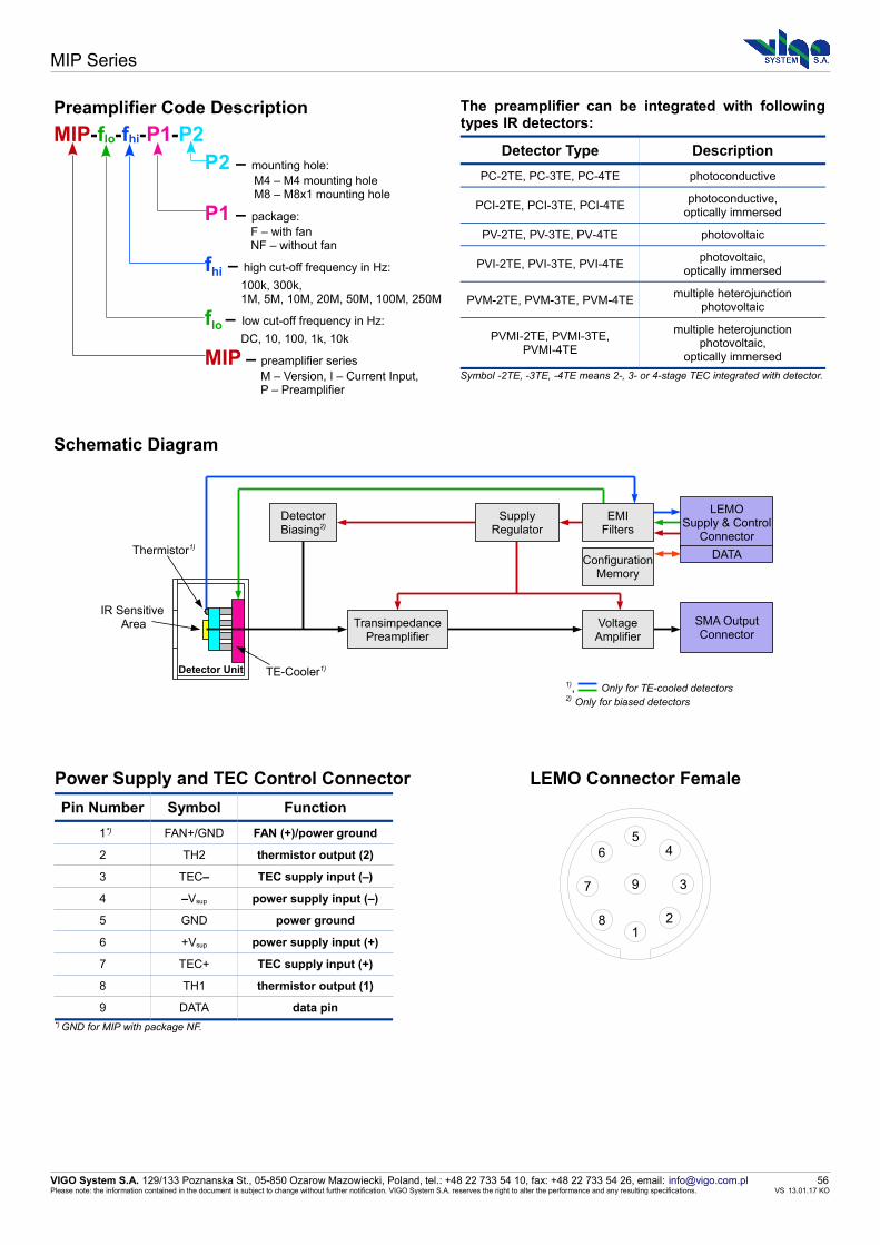
MIP Series
Preamplifier Code Description
MIP-flo-fhi-P1-P2
The preamplifier can be integrated with followingtypes IR detectors:
Detector Type Description
PC-2TE, PC-3TE, PC-4TE photoconductive
PCI-2TE, PCI-3TE, PCI-4TEphotoconductive,
optically immersed
PV-2TE, PV-3TE, PV-4TE photovoltaic
PVI-2TE, PVI-3TE, PVI-4TEphotovoltaic,
optically immersed
PVM-2TE, PVM-3TE, PVM-4TEmultiple heterojunction
photovoltaic
PVMI-2TE, PVMI-3TE,PVMI-4TE
multiple heterojunctionphotovoltaic,
optically immersed
Symbol -2TE, -3TE, -4TE means 2-, 3- or 4-stage TEC integrated with detector.
Schematic Diagram
Power Supply and TEC Control Connector
Pin Number Symbol Function
1*) FAN+/GND FAN (+)/power ground
2 TH2 thermistor output (2)
3 TEC– TEC supply input (–)
4 –Vsup power supply input (–)
5 GND power ground
6 +Vsup power supply input (+)
7 TEC+ TEC supply input (+)
8 TH1 thermistor output (1)
9 DATA data pin*) GND for MIP with package NF.
LEMO Connector Female
VIGO System S.A. 129/133 Poznanska St., 05-850 Ozarow Mazowiecki, Poland, tel.: +48 22 733 54 10, fax: +48 22 733 54 26, email: [email protected] 56Please note: the information contained in the document is subject to change without further notification. VIGO System S.A. reserves the right to alter the performance and any resulting specifications. VS 13.01.17 KO
Detector Unit
IR Sensitive Area
Thermistor1)
TE-Cooler1)
DetectorBiasing2)
SupplyRegulator
TransimpedancePreamplifier
VoltageAmplifier
EMIFilters
LEMOSupply & Control
Connector
SMA OutputConnector
1), Only for TE-cooled detectors2) Only for biased detectors
ConfigurationMemory
DATA
1
7 3
5
28
46
9
P2 – mounting hole: M4 – M4 mounting hole M8 – M8x1 mounting hole
P1 – package: F – with fan NF – without fan
fhi – high cut-off frequency in Hz:
100k, 300k, 1M, 5M, 10M, 20M, 50M, 100M, 250M
flo – low cut-off frequency in Hz:
DC, 10, 100, 1k, 10k
MIP – preamplifier series M – Version, I – Current Input, P – Preamplifier

MIP Series
Physical Dimensions [mm]
MIP package F
MIP package NF
VIGO System S.A. 129/133 Poznanska St., 05-850 Ozarow Mazowiecki, Poland, tel.: +48 22 733 54 10, fax: +48 22 733 54 26, email: [email protected] 57Please note: the information contained in the document is subject to change without further notification. VIGO System S.A. reserves the right to alter the performance and any resulting specifications. VS 13.01.17 KO

MIP Series
Recommended Accessories
PTCC-01-OEM PTCC-01-BAS PTCC-01-ADV STCC-04 MTCC-01
Programmable “Smart” TECController – OEM
Programmable “Smart” TECControler – Basic
Programmable “Smart” TECControler – Advanced
Standard TEC Controller Miniature TEC Controller
MPPS-01 SMA-BNC SMA-SMA LEMO-DB9 LEMO-DUBOX2x5
Preamplifier Power Supply Signal Output Cable Signal Output Cable TEC and Supply Cable TEC and Supply Cable
LEMO-AMP2x4 AMP1x6-MIC5 AMP1x6-POWER KK2-POWER USB: TypeA-MicroB
TEC and Supply Cable Power Supply Cable Power Supply Cable Power Supply Cable Cable for PC Connection
AC Adaptor Power Cable EU Power Cable UK Power Cable US EL-1
Power Supply Adaptor Power Cable Power Cable Power Cable Accessory Lens with Mount
DRB-1 DRB-2 MP PH STA-8x1-4
Base Mounting System Base Mounting System Mounting Post Post Holder Special Thread Adapter
VIGO System S.A. 129/133 Poznanska St., 05-850 Ozarow Mazowiecki, Poland, tel.: +48 22 733 54 10, fax: +48 22 733 54 26, email: [email protected] 58Please note: the information contained in the document is subject to change without further notification. VIGO System S.A. reserves the right to alter the performance and any resulting specifications. VS 13.01.17 KO

PIP Series PROGRAMMABLE ”SMART” PREAMPLIFIER
Features• Compact size• High signal-to-noise ratio• Dedicated for operation with 2-, 3- and 4-stage TE cooled
or uncooled detectors• Parameters settable by the user:▪ output voltage offset▪ gain (in 40 dB range)▪ bandwidth:
150 kHz, 1.5 MHz, 20 MHz1.5 MHz, 15 MHz, 200 MHz
▪ coupling AC/DC▪ detector parameters (in some cases, with limitation)
• Programmable modules and programmable controllersare interchangeable
• Highly flexible configuration allows the user to adaptthe module to variety of system parameters
• Additional accessories available
Applications• Contactless temperature measurement• Free space optical communication• Laser radiation detection• Gas analysis• Fourier spectroscopy• Fire, flame and human body detection• Pyrometers, scanners • Nondestructive material testing • OEM applications
Preamplifier Specification
Parameter Symbol Unit Typical Value Conditions, Remarks
Input Noise Voltage Density ennV√Hz
0.95 fo = 10 kHz2)
Input Noise Current Density inpA√Hz
4.51)
7.01)first stage transimpedance = 5 kΩfirst stage transimpedance = 1 kΩ
Low Cut-Off Frequency flo Hz DC/1k user configurable by software
High Cut-Off Frequency fhi Hz150k/1.5M/20M3)
1.5M/15M/200M3)maximum values, with limited range of detector
with „in circuit” filter activated
Transimpedance KiVA
250 – 25k1.25k – 125k
first stage transimpedace = 5 kΩfirst stage transimpedace = 1 kΩ
Output Impedance Rout Ω 50
Output Voltage Swing Vout V ±1 with 50 Ω load applied
Output Voltage Offset Voff mVmax ±254)
max ±10DC coupling setAC coupling set
Power Supply Voltage Vsup V ±9
Power Supply Current Isup mAtyp ±80
max ±100
Dimensions - mm×mm×mm40×81.3×4040×82.8×4040×84.3×40
width×depth×height - with 2TEwidth×depth×height - with 3TEwidth×depth×height - with 4TE
Operation Tempearture T °C +5...+35
Storage Temperature - °C -10...+50
Relative Humidity - % 10...90
Electrical characteristics @ Ta=20 °C.
1) The preamplifier noise may significantly reduce the system performance in some situations. This happens for large capacitance detectors operating at high frequencies.2) f0 – noise measurement frequency3) Depending on preamplifier option.4) Measured with equivalent resistor at the input instead of the detector. It's to avoid the environmental thermal radiation's impact.
VIGO System S.A. 129/133 Poznanska St., 05-850 Ozarow Mazowiecki, Poland, tel.: +48 22 733 54 10, fax: +48 22 733 54 26, email: [email protected] 59Please note: the information contained in the document is subject to change without further notification. VIGO System S.A. reserves the right to alter the performance and any resulting specifications. VS 13.01.17 KO
Example Assembling(see: Recommended Accessories)

PIP Series
DescriptionPIP is the programmable “smart” preamplifier. Due to the moderninternal configuration, it offers extreme flexibility combined withsuperior signal parameters and high reliability. Included voltagemonitor allows user to check the working conditions (supply voltages,detector bias voltage, first and last stage output voltage offset etc.)• User may also immediately change the gain, coupling (AC/DC),optimize the first stage transimpedance (in terms of input noiseand overall bandwidth), reduce the bandwidth down to 1.5 MHz(for supressing wideband noise and convenient weak signalobservation), and also manually or automatically supress the voltageoffset.• The optimized parameters are immediately stored into the internalEEPROM memory and automatically loaded after the power is on.• Reset to the factory settings is always available, and followingthe manual, the operation and manipulation is both: easy and safe.• In some cases, detector biasing condition may be adjusted, however,for detector safety this function is blocked in factory by default.
OperationAfter turning on the controller, blinking LEDs, or splash screenare shown (depending on the version). The PTCC-01 controller probesthe version of IR module, and when PIP is found, the content of itsinternal memory is downloaded, and following the data, proper workingconditions are set: detector temperature, module supply voltage andabove mentioned preamplifier parameters. From the user point ofview: PTCC-01 informs of cooling down the detector indicated byblinking green LOCK LED, and when the valid temperature is reached,module supply is switched on and the IR detecting set is ready tooperate.• The intelligent controller and intelligent module together constantlyprobe the working conditions and, if any potential risk is recognized(overloading the supply or TEC lines, overheating the module, openingup the temperature stabilization loop etc.) the module is being shutdown, and ERROR LED is on.• For controlling the preamplifier parameters or performing a firmwareupdate, please use the PC software. Parameters may be controlledby using PTCC-01-ADV – no PC is then necessary.
WARNING! For proper operation, PIP preamplifier integrated with IRdetector should be connected to the PTCC-01 controller.
Preamplifier Code Description
PIP-flo-fhi-P1-P2
The preamplifier can be integrated with followingtypes IR detectors:
Detector Type Description
PC, PC-2TE, PC-3TE, PC-4TE photoconductive
PCI, PCI-2TE, PCI-3TE, PCI-4TEphotoconductive,
optically immersed
PV, PV-2TE, PV-3TE, PV-4TE photovoltaic
PVI, PVI-2TE, PVI-3TE, PVI-4TEphotovoltaic,
optically immersed
PVM, PVM-2TE, PVM-3TE, PVM-4TEmultiple heterojunction
photovoltaic
PVMI, PVMI-2TE, PVMI-3TE, PVMI-4TEmultiple heterojunction
photovoltaic,optically immersed
Symbol -2TE, -3TE, -4TE means 2-, 3- or 4-stage TEC integrated with detector.No TE mark informs that the detector is not TE cooled.
Schematic Diagram
VIGO System S.A. 129/133 Poznanska St., 05-850 Ozarow Mazowiecki, Poland, tel.: +48 22 733 54 10, fax: +48 22 733 54 26, email: [email protected] 60Please note: the information contained in the document is subject to change without further notification. VIGO System S.A. reserves the right to alter the performance and any resulting specifications. VS 13.01.17 KO
Detector Unit
IR Sensitive Area
Thermistor1)
TE-Cooler1)
DetectorBiasing2)
SupplyRegulator
TransimpedancePreamplifier
VoltageAmplifier
EMIFilters
LEMOSupply & Control
Connector
SMA OutputConnector
1), Only for TE-cooled detectors2) Only for biased detectors
MicrocontrollerCPU
DATA
P2 – mounting hole: M4 – M4 mounting hole M8 – M8x1 mounting hole
P1 – package: F – with fan
fhi – high cut-off frequency in Hz:
20M, 200M
flo – low cut-off frequency in Hz:
DC/1k (user configurable by software)
PIP – preamplifier series P – Programmable, I – Current Input, P – Preamplifier

PIP Series
Power Supply and TEC Control Connector
Pin Number Symbol Function
1 FAN+ FAN (+)
2 TH2 thermistor output (2)
3 TEC– TEC supply input (–)
4 –Vsup power supply input (–)
5 GND power ground
6 +Vsup power supply input (+)
7 TEC+ TEC supply input (+)
8 TH1 thermistor output (1)
9 DATA data pin
LEMO Connector Female
Physical Dimensions [mm]
VIGO System S.A. 129/133 Poznanska St., 05-850 Ozarow Mazowiecki, Poland, tel.: +48 22 733 54 10, fax: +48 22 733 54 26, email: [email protected] 61Please note: the information contained in the document is subject to change without further notification. VIGO System S.A. reserves the right to alter the performance and any resulting specifications. VS 13.01.17 KO
1
7 3
5
28
46
9

PIP Series
Recommended Accessories
PTCC-01-OEM PTCC-01-BAS PTCC-01-ADV SMA-BNC SMA-SMA
Programmable “Smart” TECController – OEM
Programmable “Smart” TECController – Basic
Programmable “Smart” TECController – Advanced
Signal Output Cable Signal Output Cable
LEMO-DB9 LEMO-DUBOX2x5 KK2-POWER USB: TypeA-MicroB AC Adaptor
TEC and Supply Cable TEC and Supply Cable Power Supply Cable Cable for PC Connection Power Supply Adaptor
DRB-1 DRB-2 MP PH STA-8x1-4
Base Mounting System Base Mounting System Mounting Post Post Holder Special Thread Adapter
VIGO System S.A. 129/133 Poznanska St., 05-850 Ozarow Mazowiecki, Poland, tel.: +48 22 733 54 10, fax: +48 22 733 54 26, email: [email protected] 62Please note: the information contained in the document is subject to change without further notification. VIGO System S.A. reserves the right to alter the performance and any resulting specifications. VS 13.01.17 KO

SIP Series ULTRA SMALL PREAMPLIFIER
Features• Very small size• High signal-to-noise ratio• Bandwidth up to 250 MHz• Dedicated for opration with 2-, 3- and 4-stage TE cooled or uncooled
detectors• Biased and non-biased detector compatible• Adjustable gain (for bandwidth up to 100 MHz)• Fully protected against exceeding supply voltage and reversing
power supply polarity• Custom modifications upon request• Additional accessories available
SIP package TO39 SIP package TO8
DescriptionSIP is the ultra small transimpedance, AC or DC coupled preamplifier.It is dedicated for OEM applications and requires external heat sink (seeRecommended Accessories).
SIP is designed for operation with either biased or non-biased and eithercooled or uncooled detectors.
Applications• Contactless temperature measurement• Free space optical communication• Laser radiation detection• Gas analysis• Fourier spectroscopy• Fire, flame and human body detection• Pyrometers, scanners• Nondestructive material testing• OEM applications
Preamplifier Specification
Parameter Symbol Unit Typical Value Conditions, Remarks
Input Noise Voltage Density ennV
√Hz0.97 – 8.01) fo = 10 kHz2)
Input Noise Current Density inpA
√Hz0.02 – 3.51) fo = 10 kHz2)
Low Cut-Off Frequency flo HzDC
10 to 10kDC coupling setAC coupling set
High Cut-Off Frequency fhi Hz 100k to 250M
Transimpedance KiVA
up to 1×10⁵
Transimpedance RangeKi max
Ki min
- up to 5 dependent on the high cut-off frequency
Output Impedance Rout Ω 50
Output Voltage Swing Vout V±10±1
fhi ≤ 1 MHz,1 MHz < fhi ≤ 250 MHz,
RL = 1 MΩ3)
RL = 50 Ω3)
Output Voltage Offset Voff mV max ±204)
Power Supply Voltage Vsup V±15±9
fhi ≤ 1 MHz1 MHz < fhi ≤ 250 MHz
Power Supply Current Isup mA max ±50 no detector biasing
Dimensions - mm×mm×mm27×44.5×2527×49.4×25
width×depth×height – SIP package TO39width×depth×height – with 2TE, 3TE, 4TE
Electrical characteristics @ Ta = 20 °C.
1) The preamplifier noise may significantly reduce the system performance in some situations. This happens for large capacitance detectors operating at high frequencies.2) f0 – noise measurement frequency3) RL – load resistance4) Measured with equivalent resistor at the input instead of the detector. It's to avoid the environmental thermal radiation's impact.
VIGO System S.A. 129/133 Poznanska St., 05-850 Ozarow Mazowiecki, Poland, tel.: +48 22 733 54 10, fax: +48 22 733 54 26, email: [email protected] 63Please note: the information contained in the document is subject to change without further notification. VIGO System S.A. reserves the right to alter the performance and any resulting specifications. VS 13.01.17 KO

SIP Series
Preamplifier Code Description
SIP-flo-fhi-P1-P2
The preamplifier can be integrated with followingtypes IR detectors:
Detector Type Description
PC, PC-2TE, PC-3TE, PC-4TE photoconductive
PCI, PCI-2TE, PCI-3TE,PCI-4TE
photoconductive, opticallyimmersed
PV, PV-2TE, PV-3TE, PV-4TE photovoltaic
PVI, PVI-2TE, PVI-3TE,PVI-4TE
photovoltaic, optically immersed
PVM, PVM-2TE, PVM-3TE,PVM-4TE
multiple heterojunction photovoltaic
PVMI, PVMI-2TE, PVMI-3TE,PVMI-4TE
multiple heterojunctionphotovoltaic, optically immersed
Symbol -2TE, -3TE, -4TE means 2-, 3- or 4-stage TEC integrated with detector.
*) Available only for fhi to 100M.
Schematic Diagram
Power Supply and TEC Control Connector
Pin Number Symbol Function
1 –Vsup power supply input (–)
2*) TH2/N.C. thermistor output/not connected
3**) DATA/GND data pin/power ground
4*) TEC–/N.C. TEC supply input (–)/not connected
5 GND power ground
6*) TH1/N.C. thermistor output/not connected
7 +Vsup power supply input (+)
8*) TEC+/N.C. TEC supply input (+)/not connected*) N.C for SIP-flo-fhi-TO39.
**) GND for SIP-flo-fhi-TO39.
AMP2x4 Connector Male
VIGO System S.A. 129/133 Poznanska St., 05-850 Ozarow Mazowiecki, Poland, tel.: +48 22 733 54 10, fax: +48 22 733 54 26, email: [email protected] 64Please note: the information contained in the document is subject to change without further notification. VIGO System S.A. reserves the right to alter the performance and any resulting specifications. VS 13.01.17 KO
Detector Unit
IR Sensitive Area
Thermistor1)
TE-Cooler1)
DetectorBiasing2)
SupplyRegulator
TransimpedancePreamplifier
VoltageAmplifier
EMIFilters
AMP2x4Supply & Control
Connector
MMCX OutputConnector
1), Only for TE-cooled detectors2) Only for biased detectors
ConfigurationMemory
DATA
2 4 6 8
7531
P2 – gain adjustment: G – with gain adjustment*)
NG – no gain adjustment
P1 – package: TO8 – for detectors with TO8 package TO39 – for detectors with TO39 package
fhi – high cut-off frequency in Hz:
100k, 300k, 1M, 5M, 10M, 20M, 50M, 100M, 250M
flo – low cut-off frequency in Hz:
DC, 10, 100, 1k, 10k
SIP – preamplifier series S – Version, I – Current Input, P – Preamplifier
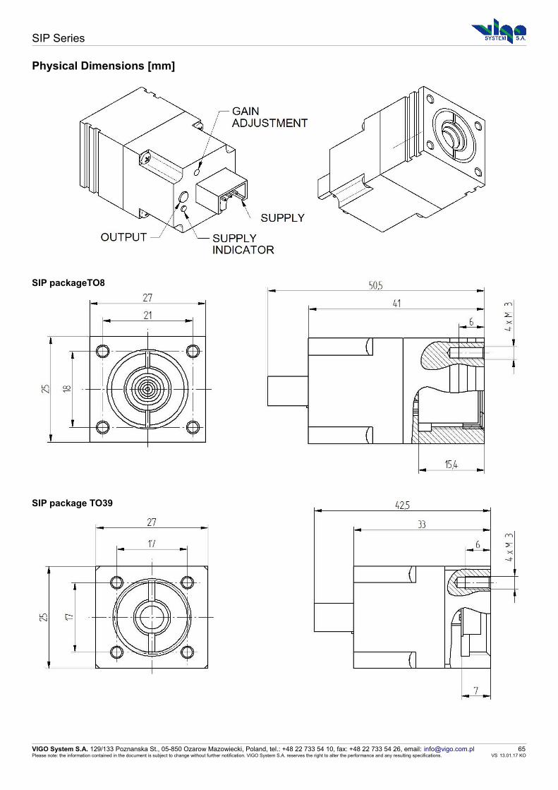
SIP Series
Physical Dimensions [mm]
VIGO System S.A. 129/133 Poznanska St., 05-850 Ozarow Mazowiecki, Poland, tel.: +48 22 733 54 10, fax: +48 22 733 54 26, email: [email protected] 65Please note: the information contained in the document is subject to change without further notification. VIGO System S.A. reserves the right to alter the performance and any resulting specifications. VS 13.01.17 KO
SIP package TO39
SIP packageTO8

SIP Series
Recommended Accessories
PTCC-01-OEM PTTC-01-BAS PTCC-01-ADV STCC-04 MTCC-01
Programmable “Smart” TECController – OEM
Programmable “Smart” TECController – Basic
Programmable “Smart” TECController – Advanced
Standard TEC Controller Miniature TEC Controller
MPPS-01 PPS-02 PPS-03 MMCX-BNC MMCX-SMA
Preamplifier Power Supply Preamplifier Power Supply Preamplifier Power Supply Signal Output Cable Signal Output Cable
AMP2x4-DB9 AMP2x4-DUBOX2x5 AMP2x4-AMP2x4 AMP2x4-MIC5 AMP1x6-MIC5
TEC and Supply Cable TEC and Supply Cable TEC and Supply Cable Power Supply Cable Power Supply Cable
AMP1x6-POWER KK2-POWER USB: TypeA-MicroB AC Adaptor Power Cable EU
Power Supply Cable Power Supply Cable Cable for PC Connection Power Supply Adaptor Power Cable
Power Cable UK Power Cable US MHS-2
Power Cable Power Cable Additional Heat Sink
VIGO System S.A. 129/133 Poznanska St., 05-850 Ozarow Mazowiecki, Poland, tel.: +48 22 733 54 10, fax: +48 22 733 54 26, email: [email protected] 66Please note: the information contained in the document is subject to change without further notification. VIGO System S.A. reserves the right to alter the performance and any resulting specifications. VS 13.01.17 KO

QIP Series FOUR CHANNEL PREAMPLIFIER
Features• Very small size• High signal-to-noise ratio• Bandwidth up to 100 MHz• Dedicated for operation with uncooled, quadrant geometry
detectors• Fully protected against exceeding supply voltage and reversing
power supply polarity• Custom configurations upon request• Additional accessories available
Applications• Laser beam positioning
DescriptionQIP is the four channel, transimpedance, AC or DC coupledpreamplifier. It is dedicated for BenchTop or OEM applications and,in some cases, requires external heat sink (see RecommendedAccessories).
QIP is designed to work with either biased or non-biased, uncooled ,quadrant geometry detectors.
Preamplifier Specification
Parameter Symbol Unit Typical Value Conditions, Remarks
Input Noise Voltage Density ennV
√Hz0.97 – 8.01) fo = 10 kHz2)
Input Noise Current Density inpA
√Hz0.02 – 3.51) fo = 10 kHz2)
Low Cut-Off Frequency flo HzDC
1k, 10kDC coupling setAC coupling set
High Cut-Off Frequency fhi Hz 100k to 100M
Transimpedance KiVA
up to 2×10⁵
Output Impedance Rout Ω 50
Output Voltage Swing Vout V ±1
Output Voltage Offset Voff mV max ±204)
Power Supply Voltage Vsup V ±9
Power Supply Current Isup mA max ±50 no detector biasing
Dimensions - mm×mm×mm 50×58.5×50 width×depth×height
Electrical characteristics @ Ta = 20 °C.
1) The preamplifier noise may significantly reduce the system performance in some situations. This happens for large capacitance detectors operating at high frequencies.2) f0 – noise measurement frequency3) RL – load resistance4) Measured with equivalent resistor at the input instead of the detector. It's to avoid the environmental thermal radiation's impact.
VIGO System S.A. 129/133 Poznanska St., 05-850 Ozarow Mazowiecki, Poland, tel.: +48 22 733 54 10, fax: +48 22 733 54 26, email: [email protected] 67Please note: the information contained in the document is subject to change without further notification. VIGO System S.A. reserves the right to alter the performance and any resulting specifications. VS 13.01.17 KO
Example Assembling(see: Recommended Accessories)

QIP Series
Preamplifier Code Description
QIP-flo-fhi-P1
The preamplifier can be integrated with followingtypes IR detectors:
Detector Type Description
PCQ*) quadrant photoconductive
PVMQ quadrant multiple heterojunction photovoltaic*) Optical area 1x1mm and 2x2mm.
Schematic Diagram
Power Supply Connector
Pin Number Symbol Function
1 –Vsup power supply input (–)
2 N.C. not connected
3 GND power ground
4 N.C. not connected
5 GND power ground
6 N.C not connected
7 +Vsup power supply input (+)
8 N.C. not connected
AMP2x4 Connector Male
VIGO System S.A. 129/133 Poznanska St., 05-850 Ozarow Mazowiecki, Poland, tel.: +48 22 733 54 10, fax: +48 22 733 54 26, email: [email protected] 68Please note: the information contained in the document is subject to change without further notification. VIGO System S.A. reserves the right to alter the performance and any resulting specifications. VS 13.01.17 KO
Detector Unit
IR Sensitive Area
DetectorBiasing*)
SupplyRegulator
TransimpedancePreamplifier
VoltageAmplifier
EMIFilters
*) Only for biased detectors
AMP2x4Supply Connector
Four MCX OutputConnectors
2 4 6 8
7531
P1 – mounting hole: M4 – M4 mounting hole M8 – M8x1 mounting hole
fhi – high cut-off frequency in Hz:
100k, 300k, 1M, 5M, 10M, 20M, 50M, 100M
flo – low cut-off frequency in Hz:
DC, 1k, 10k
QIP – preamplifier series Q – Quadrant, I – Current Input, P – Preamplifier

QIP Series
Physical Dimensions [mm]
VIGO System S.A. 129/133 Poznanska St., 05-850 Ozarow Mazowiecki, Poland, tel.: +48 22 733 54 10, fax: +48 22 733 54 26, email: [email protected] 69Please note: the information contained in the document is subject to change without further notification. VIGO System S.A. reserves the right to alter the performance and any resulting specifications. VS 13.01.17 KO

QIP Series
Recommended Accessories
MPPS-01 PPS-02 PPS-03 MCX-BNC MCX-SMA
Preamplifier Power Supply Preamplifier Power Supply Preamplifier Power Supply Signal Output Cable Signal Output Cable
AMP2x4-MIC5 AMP2x4-DB9 AC Adaptor Power Cable EU Power Cable UK
Power Supply Cable Power Supply Cable Power Supply Adaptor Power Cable Power Cable
Power Cable US DRB-1 DRB-2 MP PH
Power Cable Base Mounting System Base Mounting System Mounting Post Post Holder
STA-8x1-4
Special Thread Adapter
VIGO System S.A. 129/133 Poznanska St., 05-850 Ozarow Mazowiecki, Poland, tel.: +48 22 733 54 10, fax: +48 22 733 54 26, email: [email protected] 70Please note: the information contained in the document is subject to change without further notification. VIGO System S.A. reserves the right to alter the performance and any resulting specifications. VS 13.01.17 KO

STCC-04 Series STANDARD TEC CONTROLLER
DescriptionThe STCC-04 is a standard thermoelectric cooler controllerwith ±0.01 ºC stability.The unit provides low noise power supply for integrated preamplifiers.
Features• Provides proper detector cooling• Preamplifier power supply included• Temperature lock indicator
TEC Controller Specification
Parameter UnitValue
Conditions, RemarksMin Typ Max
Temperature Stability K ±0.01 Tdet = 233 K (-40 °C)
Detector Temperature Settling Time s25
300300
Tdet = 233 K (-40 °C), ΔTdet = 0.1 °CTdet = 213K (-60 °C), ΔTdet = 0.1 °CTdet = 193 K (-80 °C), ΔTdet = 0.1 °C
Maximum Voltage AcrossTEC Element
V2.54.07.7
STCC-04-P1-2-P3-P4STCC-04-P1-3-P3-P4STCC-04-P1-4-P3-P4
Ripple of Output Current % 0.5 ITEC = 1 A
Output Current of the Built-In Power Supply
mA ±100STCC-04-09-P2-P3-P4STCC-04-15-P2-P3-P4
Power Supply Voltage Vsup V4.511.5
5.512.5
STCC-04-P1-2-P3-P4, STCC-04-P1-3-P3-P4STCC-04-P1-4-P3-P4
Power Supply Current Isup mA3A1A
STCC-04-P1-2-P3-P4, STCC-04-P1-3-P3-P4STCC-04-P1-4-P3-P4
Series Resistanceof the Connecting Cable
mΩ 1000total resistance of the wires supplying
TEC element
Dimensions mm×mm×mm 82×60.5×150 width×height×depth
Weight kg0.250.27
STCC-04-00-P2-P3-P4remaining models
Electrical characteristics @ Ta = 20 °C.
TEC Controller Code Description
STCC-04-P1-P2-P3-P4
VIGO System S.A. 129/133 Poznanska St., 05-850 Ozarow Mazowiecki, Poland, tel.: +48 22 733 54 10, fax: +48 22 733 54 26, email: [email protected] 71Please note: the information contained in the document is subject to change without further notification. VIGO System S.A. reserves the right to alter the performance and any resulting specifications. VS 13.01.17 KO
P4 – temperature of IR detector: P5 – 278 K, +5 °C 40 – 233 K, -40 °C 60 – 213 K, -60 °C 80 – 193 K, -80 °C
P3 – type of thermistor: C – NCP03XM222E05RL (standard) B – BR14KA132J-A (only for certain types of IR detectors) A – TB04-222 (only for certain types of IR detectors)
P2 – type of TE cooler: 2 – two - stage 3 – three - stage 4 – four - stage
P1 – preamplifier power supply: 00 – no power supply 09 – power supply ±9 V 15 – power supply ±15 V G1 – combined power supply (+12 V, -5 V) for FIP preamplifier
STCC-04 – cooler controller series S – Standard, T – Thermoelectric, C – Cooler, C – Controller, ver 04

STCC-04 Series
Physical Dimensions [mm]
Power Supply and Control Connector DB9 Connector Female
Pin Number Symbol Function
1 TEC+ TEC supply output (+)
2 TEC– TEC supply output (–)
3 GND power ground
4 TH1 thermistor input (1)
5 TH2 thermistor input (2)
6 –Vsup power supply output (–)
7 FAN+/GND FAN (+)/power ground
8 N.C. not connected
9 +Vsup power supply output (+)
Recommended Accessories
AC Adaptor LEMO-DB9 AMP2x4-DB9 DB9-DB9
Power Supply Adaptor TEC and Supply Cable TEC and Supply Cable Supply Cable
VIGO System S.A. 129/133 Poznanska St., 05-850 Ozarow Mazowiecki, Poland, tel.: +48 22 733 54 10, fax: +48 22 733 54 26, email: [email protected] 72Please note: the information contained in the document is subject to change without further notification. VIGO System S.A. reserves the right to alter the performance and any resulting specifications. VS 13.01.17 KO
5 4 3 2 1
9 8 7 6

MTCC-01 Series MINIATURE TEC CONTROLLER
DescriptionThe MTCC-01 miniature TEC controller is designed to controltemperature of 2- or 3-stage TE cooled IR detectors. MTCC-01 can beused with the Integrated Detector/Preamplifier Module BIP, MIP, SIPand FIP series. The target temperature is factory adjusted in range of205 to 255K.
Features• Compact size• Low cost• Easy to use• High stability• Low power consumption• Low noise, due to the linear
regulation based on output stage
Applications
• Temperature control of TE cooled IR detectors
• OEM applications
WARNING! The TEC controller is paired in the factory with the detector delivered in the IR set. Swapping controllers may cause malfunction ordamage of TEC and detector.
TEC Controller Specification
Parameter Unit Typical Value Conditions, Remarks
Temperature Stability K ±0.01
Settling Time of the Set DetectorTemperature
s6090
MTCC-01-2TE, Tdet = 233 K (-40 °C)MTCC-01-3TE, Tdet = 213 K (-60 °C)
Power Supply Voltage Vsup V2.6 to 5.54.0 to 5.5
MTCC-01-2TEMTCC-01-3TE
Maximum TEC Output Current ITEC A1.10.43
MTCC-01-2TEMTCC-01-3TE
Maximum TEC Output Voltage VTEC V 3.6
Dimensions mm×mm×mm 70×45×19 width×height×depth
Weight g 35Electrical characteristics @ Ta = 20 °C.
TEC Controller Code Description
MTCC-01-P1
Example Wiring Diagram
VIGO System S.A. 129/133 Poznanska St., 05-850 Ozarow Mazowiecki, Poland, tel.: +48 22 733 54 10, fax: +48 22 733 54 26, email: [email protected] 73Please note: the information contained in the document is subject to change without further notification. VIGO System S.A. reserves the right to alter the performance and any resulting specifications. VS 13.01.17 KO
BIP, MIP, SIP, FIPIntegrated Preamplifier
MPPS-01Linear Power
Supply
SMA-BNCCable
AMP2x4-AMP2x4Cable
J1
J2
MTCC-01 TEC Controller
100..240VAC50..60Hz
To Oscilloscope
AMP1x6-MIC5Cable
P1 – number of TE cooler stages: 2TE – two - stage 3TE – three - stage
MTCC-01 – cooler controller series: M - Miniature, T - Thermoelectric, C - Cooler, C - Controller, ver 01

MTCC-01 Series
Physical Dimensions [mm]
Power Supply and Control Connectors
AMP1x6 Connector Male (J1) AMP2x4 Connector Male (J2)
Pin Number Symbol Function
1 TECC+ TEC controller supply input (+)
2 TECC GND1) TEC controller power ground
3 +Vsup2), 3) power supply input (+)
4 GND1), 3) power ground
5 FAN+/N.C. FAN(+)/not connected
6 –Vsup2), 3) power supply input (–)
1) TECC GND and GND should be connected together in power adapter.2) See preamplifier specification for details.3) Only for preamplifier module supply, not required for proper controlleroperation.
For more details about TE cooling see Infrared Detectors DataSheets.
WARNING! Do not connect TEC– or TEC+ to any other supply orto GND!
Pin Number Symbol Function
1 –Vsup power supply output (–)
2 TH21) thermistor input (2)
3 FAN+/N.C. fan supply/not connected
4 TEC– TEC supply output (–)
5 GND power ground
6 TH11) thermistor input (1)
7 +Vsup power supply output (+)
8 TEC+ TEC supply output (+)1) Thermistor polarity without significance.
VIGO System S.A. 129/133 Poznanska St., 05-850 Ozarow Mazowiecki, Poland, tel.: +48 22 733 54 10, fax: +48 22 733 54 26, email: [email protected] 74Please note: the information contained in the document is subject to change without further notification. VIGO System S.A. reserves the right to alter the performance and any resulting specifications. VS 13.01.17 KO
1 2 3 4 5 6
2 4 6 8
7531

MTCC-01 Series
Recommended Accessories
MPPS-01 LEMO-AMP2x4 AMP2x4-AMP2x4 AMP1x6-MIC5 AMP1x6-POWER
Preamplifier Power Supply TEC and Supply Cable TEC and Supply Cable Power Supply Cable Power Supply Cable
Power Cable EU Power Cable UK Power Cable US
Power Cable Power Cable Power Cable
VIGO System S.A. 129/133 Poznanska St., 05-850 Ozarow Mazowiecki, Poland, tel.: +48 22 733 54 10, fax: +48 22 733 54 26, email: [email protected] 75Please note: the information contained in the document is subject to change without further notification. VIGO System S.A. reserves the right to alter the performance and any resulting specifications. VS 13.01.17 KO

PTCC-01 PROGRAMMABLE ”SMART” TEC CONTROLLER
PTCC-01-OEM PTCC-01-BAS PTCC-01-ADVDescriptionPTCC-01 is the programmable, precision, low noise, thermoelectric cooler controller series, designed to operate with VIGO IR detection modules.It is compatible with both classic (BIP, MIP, SIP, FIP) and new, programmable PIP preamplifiers, integrated with IR detectors. Available options:
PTCC-01-OEM PTCC-01-BAS PTCC-01-ADV
• TEC controller and preamplifier power supplywithout housing
• Configurable by PC software available on webpage
• Status LED indicator and status/dataconnector
• TEC controller and preamplifier power supplyencapsulated in a small size enclosure
• Configurable by PC software available on webpage
• Status LED indicator
• TEC controller and preamplifier power supplyencapsulated in a small size enclosure
• Configurable by build-in function keys or PCsoftware available on web page
• Status LCD indicator
Features• Low cost• Easy to use• Very small size• Low power consumption• High stability and precision• Dedicated for opeartion with preamplifiers integrated with with 2-, 3-,
and 4-stage TE cooled detectors• Compatible with every variant of programmable preamplifier PIP;
user can swap the modules and controllers
• Modern architecture with digitally performed PID temperature control• Current / voltage / temperature monitor available with PC program• Overcurrent, overvoltage and overheating protection• Split grounds and filtering for EMC improvement• Firmware upgrade option available• Provides proper detector cooling• Preamplifier supply included
TEC Controller Specification
Parameter UnitValue
Conditions, RemarksMin Typ Max
Temperature Stability K ±0.01 Tdet = 233 K (-40 °C)
Temperature Readout Stability mK 1 Tdet = 213 K (-60 °C)
Detector Temperature Settling Time s254560
Tdet = 233 K (-40 °C),Tdet = 213 K (-60 °C),Tdet = 193 K (-80 °C),
ΔTdet = 0.1 KΔTdet = 0.1 KΔTdet = 0.1 K
Maximum TEC Current A1.2
0.450.45
2TE3TE4TE
Output Voltage Range V 3 14.5
Output Current of The Built-InPower Supply
mA ±200 output voltage: 3…14.5 V
Power Supply Voltage Vsup V 9 16 wider range available on demand
Power Supply Current Isup mA 500 ITEC = 0.45 A, UTEC = 7.5 V
Series Resistanceof the Connecting Cable
mΩ 1000total resistance of the wires supplying TEC
element
Dimensions mm×mm×mm51×17.3×93
55×24.2×111.868.9×30.4×107.8
width×height×depth - PTCC-01-OEMwidth×height×depth - PTCC-01-BASwidth×height×depth - PTCC-01-ADV
Weight g51155190
PTCC-01-OEMPTCC-01-BASPTCC-01-ADV
Storage Temperature °C -20 +70
Ambient Temperature °C +5 +45
Relative Humidity %1010
9050
from +5 °C to +35 °C> +35 °C
Electrical characteristics @ Ta = 20 °C.
VIGO System S.A. 129/133 Poznanska St., 05-850 Ozarow Mazowiecki, Poland, tel.: +48 22 733 54 10, fax: +48 22 733 54 26, email: [email protected] 76Please note: the information contained in the document is subject to change without further notification. VIGO System S.A. reserves the right to alter the performance and any resulting specifications. VS 13.01.17 KO

PTCC-01 Series
Physical Dimensions [mm]
PTCC-01-OEM
PTCC-01-BAS
PTCC-01-ADV
VIGO System S.A. 129/133 Poznanska St., 05-850 Ozarow Mazowiecki, Poland, tel.: +48 22 733 54 10, fax: +48 22 733 54 26, email: [email protected] 77Please note: the information contained in the document is subject to change without further notification. VIGO System S.A. reserves the right to alter the performance and any resulting specifications. VS 13.01.17 KO
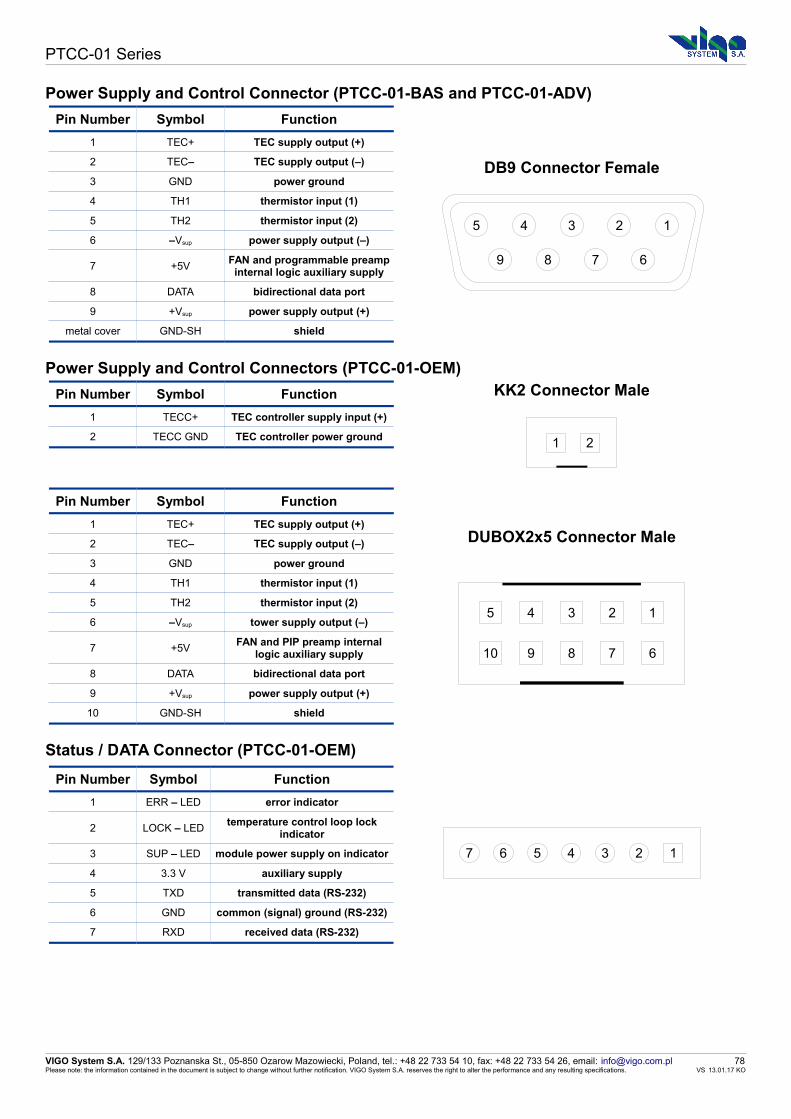
PTCC-01 Series
Power Supply and Control Connector (PTCC-01-BAS and PTCC-01-ADV)
Pin Number Symbol Function
1 TEC+ TEC supply output (+)
2 TEC– TEC supply output (–)
3 GND power ground
4 TH1 thermistor input (1)
5 TH2 thermistor input (2)
6 –Vsup power supply output (–)
7 +5VFAN and programmable preampinternal logic auxiliary supply
8 DATA bidirectional data port
9 +Vsup power supply output (+)
metal cover GND-SH shield
DB9 Connector Female
Power Supply and Control Connectors (PTCC-01-OEM)
Pin Number Symbol Function
1 TECC+ TEC controller supply input (+)
2 TECC GND TEC controller power ground
KK2 Connector Male
Pin Number Symbol Function
1 TEC+ TEC supply output (+)
2 TEC– TEC supply output (–)
3 GND power ground
4 TH1 thermistor input (1)
5 TH2 thermistor input (2)
6 –Vsup tower supply output (–)
7 +5VFAN and PIP preamp internal
logic auxiliary supply
8 DATA bidirectional data port
9 +Vsup power supply output (+)
10 GND-SH shield
DUBOX2x5 Connector Male
Status / DATA Connector (PTCC-01-OEM)
Pin Number Symbol Function
1 ERR – LED error indicator
2 LOCK – LEDtemperature control loop lock
indicator
3 SUP – LED module power supply on indicator
4 3.3 V auxiliary supply
5 TXD transmitted data (RS-232)
6 GND common (signal) ground (RS-232)
7 RXD received data (RS-232)
VIGO System S.A. 129/133 Poznanska St., 05-850 Ozarow Mazowiecki, Poland, tel.: +48 22 733 54 10, fax: +48 22 733 54 26, email: [email protected] 78Please note: the information contained in the document is subject to change without further notification. VIGO System S.A. reserves the right to alter the performance and any resulting specifications. VS 13.01.17 KO
5 4 3 2 1
9 8 7 6
1 2
5 4 3 2 1
10 9 8 7 6
17 23456

PTCC-01 Series
Recommended Accessories
AMP2x4-DB9 AMP2x4-DUBOX2x5 LEMO-DB9 LEMO-DUBOX2x5 KK2-POWER
TEC and Supply Cable TEC and Supply Cable TEC and Supply Cable TEC and Supply Cable Power Supply Cable
USB: TypeA-MicroB AC Adaptor
Cable for PC Connection Power Supply Adaptor
VIGO System S.A. 129/133 Poznanska St., 05-850 Ozarow Mazowiecki, Poland, tel.: +48 22 733 54 10, fax: +48 22 733 54 26, email: [email protected] 79Please note: the information contained in the document is subject to change without further notification. VIGO System S.A. reserves the right to alter the performance and any resulting specifications. VS 13.01.17 KO

PPS-02 Series PREAMPLIFIER POWER SUPPLY
DescriptionThe PPS-02 preamplifier power supply is designed forsupplying VIGO System IR Detection Modules includeduncooled IR detectors.
Features• Dedicated for supplying uncooled detectors• Compact size• Easy to use• Low cost
Preamplifier Power Supply Specification
Parameter Unit Value Conditions, Remarks
Power Supply Voltage Vsup V AC 100 to 240 50 to 60 Hz
Output Voltage V DC±15±9
+12, -5
Output Current mA ±100
Dimensions mm×mm×mm 82×60.5×150 width×height×depth
Weight kg 0.25Electrical characteristics @ Ta = 20 °C.
Preamplifier Power Supply Code Description
PPS-02-P1
Power Supply Connector
Pin Number Symbol Function
1 N.C. not connected
2 N.C. not connected
3 GND power ground
4 N.C. not connected
5 N.C. not connected
6 –Vsup power supply output (–)
7 N.C. not connected
8 N.C. not connected
9 +Vsup power supply output (+)
DB9 Connector Female
VIGO System S.A. 129/133 Poznanska St., 05-850 Ozarow Mazowiecki, Poland, tel.: +48 22 733 54 10, fax: +48 22 733 54 26, email: [email protected] 80Please note: the information contained in the document is subject to change without further notification. VIGO System S.A. reserves the right to alter the performance and any resulting specifications. VS 13.01.17 KO
5 4 3 2 1
9 8 7 6
P1 – power supply: 09 – power supply ±9 V 15 – power supply ±15 V G1 – combined power supply (+12 V, -5 V) for FIP preamplifier
PPS-02 – preamplifier power supply series P – Preamplifier, P – Power, S – Supply, ver 02

PPS-02 Series
Physical Dimensions [mm]
Recommended Accessories
AC Adaptor LEMO-DB9 AMP2x4-DB9 DB9-DB9
Power Supply Adaptor Supply Cable Supply Cable Supply Cable
VIGO System S.A. 129/133 Poznanska St., 05-850 Ozarow Mazowiecki, Poland, tel.: +48 22 733 54 10, fax: +48 22 733 54 26, email: [email protected] 81Please note: the information contained in the document is subject to change without further notification. VIGO System S.A. reserves the right to alter the performance and any resulting specifications. VS 13.01.17 KO

PPS-03 Series PREAMPLIFIER POWER SUPPLY
DescriptionThe PPS-03 preamplifier power supply is designed forsupplying VIGO System IR Detection Modules includeduncooled IR detectors.
Features• Dedicated for supplying uncooled detectors• Very small size• Low cost
Preamplifier Power Supply Specification
Parameter Unit Value Conditions, Remarks
Power Supply Voltage Vsup V AC 100 to 240 50 to 60 Hz
Output Voltage V DC±15±9
+12, -5
Output Current mA ±100
Dimensions mm×mm×mm 55×24.2×54 width×height×depth
Weight g 100Electrical characteristics @ Ta = 20 °C.
Preamplifier Power Supply Code Description
PPS-03-P1
Power Supply Connector
Pin Number Symbol Function
1 N.C. not connected
2 N.C. not connected
3 GND power ground
4 N.C. not connected
5 N.C. not connected
6 –Vsup power supply output (–)
7 N.C. not connected
8 N.C. not connected
9 +Vsup power supply output (+)
DB9 Connector Female
VIGO System S.A. 129/133 Poznanska St., 05-850 Ozarow Mazowiecki, Poland, tel.: +48 22 733 54 10, fax: +48 22 733 54 26, email: [email protected] 82Please note: the information contained in the document is subject to change without further notification. VIGO System S.A. reserves the right to alter the performance and any resulting specifications. VS 13.01.17 KO
5 4 3 2 1
9 8 7 6
P1 – power supply: 09 – power supply ±9 V 15 – power supply ±15 V G1 – combined power supply (+12 V, -5 V) for FIP preamplifier
PPS-03 – preamplifier power supply series P – Preamplifier, P – Power, S – Supply, ver 03

PPS-03 Series
Physical Dimensions [mm]
Recommended Accessories
AC Adaptor LEMO-DB9 AMP2x4-DB9 DB9-DB9
Power Supply Adaptor Supply Cable Supply Cable Supply Cable
VIGO System S.A. 129/133 Poznanska St., 05-850 Ozarow Mazowiecki, Poland, tel.: +48 22 733 54 10, fax: +48 22 733 54 26, email: [email protected] 83Please note: the information contained in the document is subject to change without further notification. VIGO System S.A. reserves the right to alter the performance and any resulting specifications. VS 13.01.17 KO

MPPS-01 Series PREAMPLIFIER LINEAR POWER SUPPLY
DescriptionThe MPPS-01 preamplifier linear power supply isdesigned for supplying VIGO System IR DetectionModules included uncooled and cooled (operate withMTCC-01 controllers) IR detectors.
Features• Provides low noise preamplifier linear power supply• Dedicated for supplying uncooled and cooled IR
detectors• Easy to use
Preamplifier Power Supply Specification
Parameter Unit Value Conditions, Remarks
Power Supply Voltage Vsup V AC (100 ÷ 127) to (200 ÷ 240) 50 to 60 Hz
Output Voltage V DC±15±9
+12, -5
Output Current mA ±500
Dimensions mm×mm×mm 109×65×175 width×height×depth
Weight kg 1.3Electrical characteristics @ Ta = 20 °C.
Preamplifier Power Supply Code Description
MPPS-01-P1
Power Supply Connector
Pin Number Symbol Function
1 TEC– TEC supply output (–)
2 +Vsup power supply output (+)
3 GND power ground
4 –Vsup power supply output (–)
5 TEC+ TEC supply output (+)
MIC5 Connector Female
VIGO System S.A. 129/133 Poznanska St., 05-850 Ozarow Mazowiecki, Poland, tel.: +48 22 733 54 10, fax: +48 22 733 54 26, email: [email protected] 84Please note: the information contained in the document is subject to change without further notification. VIGO System S.A. reserves the right to alter the performance and any resulting specifications. VS 13.01.17 KO
3
51
2 4
P1 – power supply: 09 – power supply ±9 V 15 – power supply ±15 V G1 – combined power supply (+12 V, -5 V) for FIP preamplifier
MPPS-01 – preamplifier power supply series M – Version, P – Preamplifier, P - Power, S - Supply, ver 01
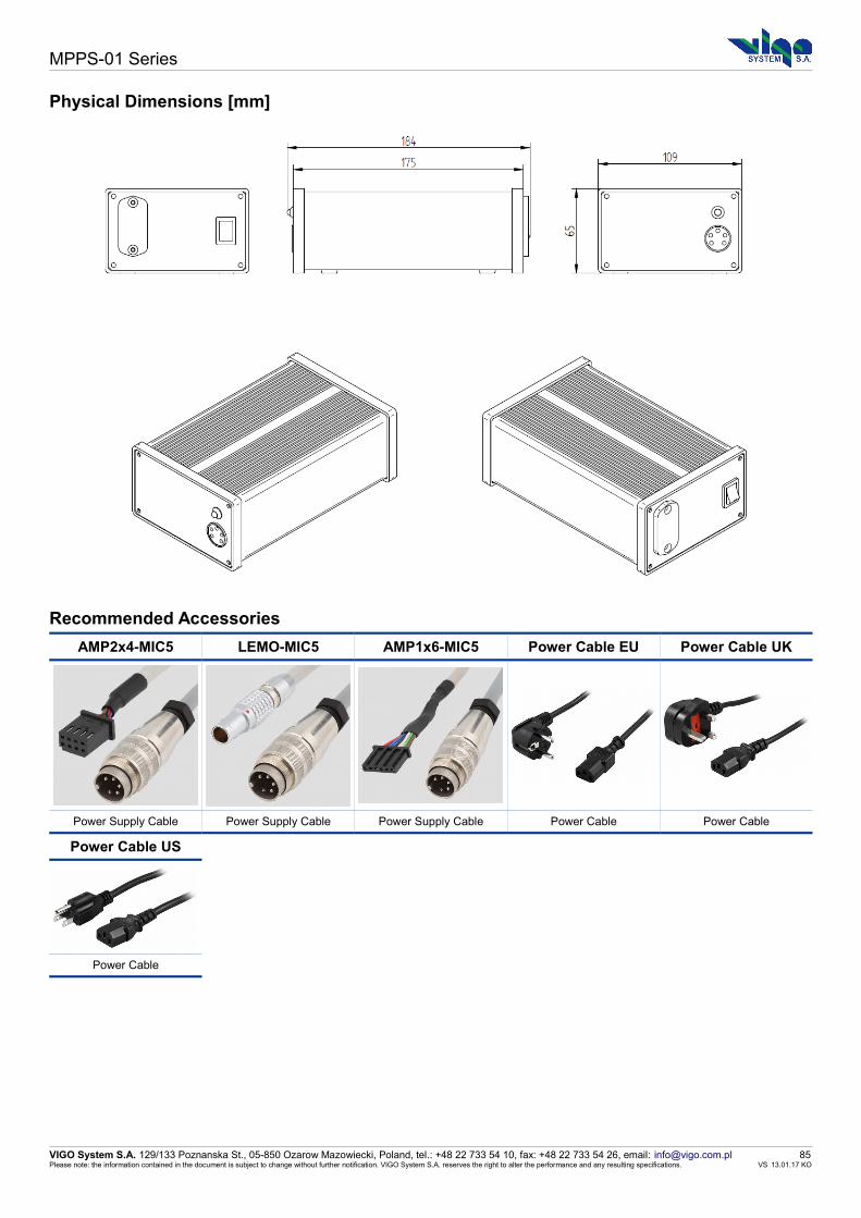
MPPS-01 Series
Physical Dimensions [mm]
Recommended Accessories
AMP2x4-MIC5 LEMO-MIC5 AMP1x6-MIC5 Power Cable EU Power Cable UK
Power Supply Cable Power Supply Cable Power Supply Cable Power Cable Power Cable
Power Cable US
Power Cable
VIGO System S.A. 129/133 Poznanska St., 05-850 Ozarow Mazowiecki, Poland, tel.: +48 22 733 54 10, fax: +48 22 733 54 26, email: [email protected] 85Please note: the information contained in the document is subject to change without further notification. VIGO System S.A. reserves the right to alter the performance and any resulting specifications. VS 13.01.17 KO

CABLES
BNC-BNC SMA-BNC SMA-SMA MMCX-BNC MMCX-SMA
Signal Input or Output Cable Signal Output Cable Signal Output Cable Signal Output Cable Signal Output Cable
MCX-BNC MCX-SMA AMP2x4-DB9 AMP2x4-DUBOX2x5 AMP2x4-AMP2x4
Signal Output Cable Signal Output Cable TEC and Supply Cable TEC and Supply Cable TEC and Supply Cable
LEMO-DB9 LEMO-DUBOX2x5 LEMO-AMP2x4 AMP1x6-MIC5 AMP1x6-POWER
TEC and Supply Cable TEC and Supply Cable TEC and Supply Cable Power Supply Cable Power Supply Cable
DB9-DB9 DB9-4mmPLUGS DB9-MIC5 AMP2x4-MIC5 LEMO-MIC5
Power Supply Cable Power Supply Cable Power Supply Cable Power Supply Cable Power Supply Cable
KK2-POWER USB: TypeA-MicroB Power Cable EU Power Cable UK Power Cable US
Power Supply Cable Cable for PC Connection Power Cable Power Cable Power Cable
VIGO System S.A. 129/133 Poznanska St., 05-850 Ozarow Mazowiecki, Poland, tel.: +48 22 733 54 10, fax: +48 22 733 54 26, email: [email protected] 86Please note: the information contained in the document is subject to change without further notification. VIGO System S.A. reserves the right to alter the performance and any resulting specifications. VS 13.01.17 KO
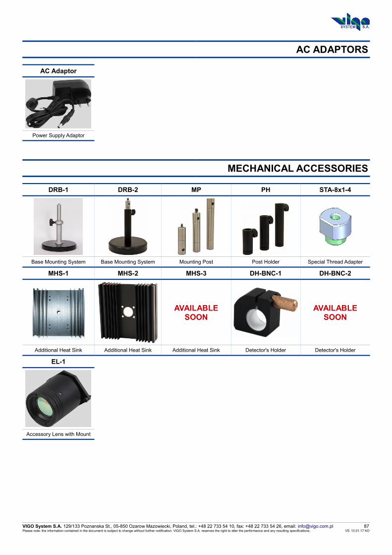
AC ADAPTORS
AC Adaptor
Power Supply Adaptor
MECHANICAL ACCESSORIES
DRB-1 DRB-2 MP PH STA-8x1-4
Base Mounting System Base Mounting System Mounting Post Post Holder Special Thread Adapter
MHS-1 MHS-2 MHS-3 DH-BNC-1 DH-BNC-2
AVAILABLESOON
AVAILABLESOON
Additional Heat Sink Additional Heat Sink Additional Heat Sink Detector's Holder Detector's Holder
EL-1
Accessory Lens with Mount
VIGO System S.A. 129/133 Poznanska St., 05-850 Ozarow Mazowiecki, Poland, tel.: +48 22 733 54 10, fax: +48 22 733 54 26, email: [email protected] 87Please note: the information contained in the document is subject to change without further notification. VIGO System S.A. reserves the right to alter the performance and any resulting specifications. VS 13.01.17 KO

DRB-1 BASE MOUNTING SYSTEM
DescriptionDRB-1 is a stable base mountig system dedicated forBench-Top IR Detection Modules and IR detectors in BNCpackages.
Features• Stable construction• Adjustable height• Durable, chrome plated elements
Specification
Parameter Value
Weight [g] 1390
Usable Height [mm] 108..178
Base Plate Diameter [mm] 120
Mounting Post Weight [g] 126
Thread M8x1 or 1/4-20 UNC
Physical Dimensions [mm]
… ...
VIGO System S.A. 129/133 Poznanska St., 05-850 Ozarow Mazowiecki, Poland, tel.: +48 22 733 54 10, fax: +48 22 733 54 26, email: [email protected] 88Please note: the information contained in the document is subject to change without further notification. VIGO System S.A. reserves the right to alter the performance and any resulting specifications. VS 13.01.17 KO

DRB-2 BASE MOUNTING SYSTEM
DescriptionDRB-2 is a stable base mountig system dedicated forBench-Top IR Detection Modules and IR detectors in BNCpackages.
Standard DRB-2 consists of:
• Base Plate BP• Mounting Post MP-100• Post Holder PH-100
IMPORTANT NOTE! If you require another dimensions ofMP or PH, please make remark in your formal purchaseorder.
Features• Stable construction• Adjustable height• Durable elements• Compatible with M6 optical breadboards
VIGO System S.A. 129/133 Poznanska St., 05-850 Ozarow Mazowiecki, Poland, tel.: +48 22 733 54 10, fax: +48 22 733 54 26, email: [email protected] 89Please note: the information contained in the document is subject to change without further notification. VIGO System S.A. reserves the right to alter the performance and any resulting specifications. VS 13.01.17 KO
Example Assembling
Thread Adapter M4-M6TA-4-6
Post HolderPH
Base PlateBP
Mounting PostMP
Special Thread Adapter M8x1-M4STA-8x1-4 (optional)
Wing Knob M4WK-4

MP MOUNTING POST
DescriptionMP is a mounting post made of stainless steel.It is equipped with two thread adapters TA-4-6as a standard.
MP-50, MP-75 and MP-100 models are available.
Specification
Model Weight [g] Dimension A [mm]
MP-50 55 50
MP-75 85 75
MP-100 115 100
Physical Dimensions [mm]
Mounting Post Thread Adapter M4-M6 (TA-4-6)
VIGO System S.A. 129/133 Poznanska St., 05-850 Ozarow Mazowiecki, Poland, tel.: +48 22 733 54 10, fax: +48 22 733 54 26, email: [email protected] 90Please note: the information contained in the document is subject to change without further notification. VIGO System S.A. reserves the right to alter the performance and any resulting specifications. VS 13.01.17 KO
Example Assembling

PH POST HOLDER
DescriptionPH is a post holder made of black anodizedaluminium. It is equipped with wink knob WK-4as a standard.
PH-50, PH-75 and PH-100 models are available.
Specification
Model Weight [g] Dimension A [mm]
PH-50 35 50
PH-75 50 75
PH-100 60 100
Physical Dimensions [mm]
VIGO System S.A. 129/133 Poznanska St., 05-850 Ozarow Mazowiecki, Poland, tel.: +48 22 733 54 10, fax: +48 22 733 54 26, email: [email protected] 91Please note: the information contained in the document is subject to change without further notification. VIGO System S.A. reserves the right to alter the performance and any resulting specifications. VS 13.01.17 KO
Example Assembling

BP BASE PLATE
DescriptionBP is a base plate made of black, lacquered steel. It providesmechanical stable conditions for mounting system.
Weight: 1756g
Physical Dimensions [mm]
VIGO System S.A. 129/133 Poznanska St., 05-850 Ozarow Mazowiecki, Poland, tel.: +48 22 733 54 10, fax: +48 22 733 54 26, email: [email protected] 92Please note: the information contained in the document is subject to change without further notification. VIGO System S.A. reserves the right to alter the performance and any resulting specifications. VS 13.01.17 KO

STA-8x1-4 SPECIAL THREAD ADAPTER
DescriptionSTA-8x1-4 is a special thread adapter M8x1 to M4, made of stainlesssteel. It allows to install Detection Modules with M8x1 mounting holeand Detector's Holder DH-BNC-1 on Base Mounting System DRB-2.
Weight: 6g
Physical Dimensions [mm]
VIGO System S.A. 129/133 Poznanska St., 05-850 Ozarow Mazowiecki, Poland, tel.: +48 22 733 54 10, fax: +48 22 733 54 26, email: [email protected] 93Please note: the information contained in the document is subject to change without further notification. VIGO System S.A. reserves the right to alter the performance and any resulting specifications. VS 13.01.17 KO

WARRANTY
VIGO System S.A. hereby represents and warrants all Products manufactured by VIGO and sold hereunder to be free from defects in workmanshipor material during a period of twelve (12) months from the date of delivery save for products for which a special warranty is given. If any Productproves however to be defective in workmanship or material within the period herein provided VIGO System undertakes to the exclusion of any otherremedy to repair or at its own option replace the defective Product or part thereof free of charge and otherwise on the same conditions as for theoriginal Product or part without extension to original warranty time. Defective parts replaced in accordance with this clause shall be placedat the disposal of VIGO.
VIGO also warrants the quality of all repair and service works performed by its employees to products sold by it. In case the repair or service worksshould appear inadequate or faulty and should this cause malfunction or nonfunctioning of the product to which the service was performed VIGOshall at its free option either repair or have repaired or replace the product in question. The working hours used by employees of VIGO for suchrepair or replacement shall be free of charge to the client. This service warranty shall be valid for a period of six (6) months from the date the servicemeasures were completed.
This warranty is however subject to following conditions:• a substantiated written claim as to any alleged defects shall have been received by VIGO System within thirty (30) days after the defect or
fault became known or occurred,and
• the allegedly defective Product or part shall, should VIGO so require, be sent to the works of VIGO or to such other place as VIGO mayindicate in writing, freight and insurance prepaid, properly packed and labeled.
This warranty does not however apply when the defect has been caused through1. normal wear and tear or accident;2. misuse or other unsuitable or unauthorized use of the Product or negligence or error in storing, maintaining or in handling the Product or
any equipment thereof;3. wrong installation, assembly or failure to service the Product or otherwise follow VIGO's service instructions including any repairs or
installation or assembly or service made by unauthorized personnel not approved by VIGO or replacements with parts not manufacturedor supplied by VIGO;
4. modifications or changes of the Product as well as any adding to it without VIGO's prior authorization;5. burned active element by irradiation above damage thresholds;6. electrostatic discharges;7. improper detector bias;8. improper TE cooler bias (TE cooler damage or active element overheating);9. other factors dependent on the Customer or a third party.
Notwithstanding the aforesaid VIGO System liability under this clause shall not apply to any defects arising out of materials, designs or instructionsprovided by the Customer.
This warranty is expressly in lieu of and excludes all other conditions, warranties and liabilities, expressed or implied, whether under law, statute orotherwise, including without limitation any implied warranties of merchantability or fitness for a particular purpose and all other obligations andliabilities of VIGO or its representatives with respect to any defect or deficiency applicable to or resulting directly or indirectly from the Productssupplied hereunder, which obligations and liabilities are hereby expressly canceled and waived. VIGO's liability shall under no circumstances exceedthe invoice price of any Product for which a warranty claim is made, nor shall VIGO in any circumstances be liable for lost profits or otherconsequential loss whether direct or indirect or for special damage.
RMA Request Instructions: • No Product may be returned without first contacting VIGO for a Return Material Authorization ('RMA') number.• Please obtain a RMA number from VIGO Support Team before returning any item. When requesting a RMA number, please state your
order number, the product you wish to return and the reason for return. We will only accept returns which have an RMA number.Authorized returns are to be shipped according to received instruction from VIGO in appropriate shipping box. An unauthorized return, i.e.one for which an RMA number has not been issued and authorized returns however, shipped with incorrect customs documents - will notbe accepted.
• Please print the RMA number clearly on the return label to avoid any delay in processing. Please send package to:
VIGO System S.A.Sales Office, Building B129/133 Poznanska St.
05-850 Ozarow MazowieckiPOLAND
VIGO System S.A. 129/133 Poznanska St., 05-850 Ozarow Mazowiecki, Poland, tel.: +48 22 733 54 10, fax: +48 22 733 54 26, email: [email protected] 94Please note: the information contained in the document is subject to change without further notification. VIGO System S.A. reserves the right to alter the performance and any resulting specifications. VS 13.01.17 KO

CONTACT AND DISTRIBUTORS
Find Our Products in Your CountryTo find our representative in your local area, please check the table below. If you do not find a Distributor listed in your country, please contact usdirectly:
VIGO System S.A.129/133 Poznanska Str.05-850 Ozarow MazowieckiPOLANDtel.: +48 22 733 54 06fax: +48 22 733 54 26email: [email protected]://www.vigo.com.pl
CHINA CHINA FRANCE
BIT Photoelectronic Co., Ltdtel.: +86 10 6891 3630fax: +86 10 6847 0197
email: [email protected]://www.bitpe.com
Uniqueray Technologies Limitedtel.: +86 755 2333 9831fax: +86 755 2333 9831mobile: +86 180 3808 5221email: [email protected]
ACAL BFI FRANCEtel.: +33 (0) 1 60 79 59 30fax: +33 (0) 1 60 79 89 01
email: [email protected]
GERMANY ISRAEL ITALY
DoroTEK GmbHtel.: + 49(0)3341 21 54 27fax: 49(0)3341 21 54 29
email: i [email protected]://www.dorotek.de
Bi-Poltel.: +972 525 877 759
email: [email protected]
Massimo Bonfantetel.: +39 02 36 52 46 30fax: +39 02 99 98 12 25mobile: +39 335 82 22 917email: [email protected]://www.masbonfante.it
JAPAN JAPAN MEXICO & COLOMBIA
FIT Leadintex, Inc.tel.: +81 3 3666 7100fax: +81 3 3666 7007
email: [email protected]://www.fit-leadintex.jp
IR System Co., Ltd.tel.: +81 42 400 0373fax: +81 42 400 0374 email: [email protected]
Mexitek, S.A. tel.: +52 55 5575 0312
email: [email protected]
NETHERLANDS UNITED KINGDOM USA & CANADA
Jonat Automation B.V.tel.: +31 (0)13 571 16 26fax: +31 (0)13 571 55 88mobile: +31 (0)6 24 802 956email: [email protected]://www.jonat.com
Photonic Solutions, LTdtel: +44 (0)131 664 8122fax: +44 (0)131 449 7301
email: [email protected]://www.photonicsolutions.co.uk/
Boston Electronics Corporationtel.: (617) 566 3821fax: (617) 731 0935
email: [email protected]://www.boselec.com
Would You Like To Be Our Distributor?In order to increase our presence in the global market, we are looking for prospective partners for distribution of our products. For more information, please contact us.
VIGO System S.A. 129/133 Poznanska St., 05-850 Ozarow Mazowiecki, Poland, tel.: +48 22 733 54 10, fax: +48 22 733 54 26, email: [email protected] 95Please note: the information contained in the document is subject to change without further notification. VIGO System S.A. reserves the right to alter the performance and any resulting specifications. VS 13.01.17 KO

Appendix
VIGO System S.A. 129/133 Poznanska St., 05-850 Ozarow Mazowiecki, Poland, tel.: +48 22 733 54 10, fax: +48 22 733 54 26, email: [email protected] 96Please note: the information contained in the document is subject to change without further notification. VIGO System S.A. reserves the right to alter the performance and any resulting specifications. VS 13.01.17 KO

UNIT: mmGENERAL TOLERANCE:
X.X=±0.1 / X.XX=±0.05
18-Jul-16
TITLE:Detector TO8 - XTE
SIZE
A4
DWG NO:
DT-TO8-XTE.003SCALE:
WEIGHT:
SHEET 1 OF 12:1
Date:No.
123
4
5
6
7
NameTO8 housing
Detector case
Absorber container
Detector cap
Window
Detector on sapphire pad
Thermo-electic cooler
7u1 g
Material
Gold plated Kovar
Stainless steelStainlesl steel
Stainless steel
Al2O3 / ZnSe / other
HgCdTe / GaAs / Sapphire
8 4-40 UNC A2 screw
The drawings and the information provided with the drawings are the soleproperty of VIGO System S.A. Any disclosure or reproduction, in part or whole,without the written permission of VIGO System S.A. is prohibited.
VIGO System's detectors contains miniature amounts of mercury and cadmium butas part of medical devices, monitoring and control instruments can be treated asan exempt from the UE Directive on the Restriction of Hazardous Substances (RoHS).
Production Department
15.2 ±0.2O6O
7.8
±0.3
6.4
±0.4
A
B
C
0.45O
F
4-40 UNC
5.08
10.16
5.08
10.16
11
12
10
9
123
4
5
6 7 8
FOV
1
2
3
45
6
7
Two-stage thermoelectric cooler - 2TELens shape Hyperhemisphere Hemisphere Flat
Detector optical area [mm²] 0.5x0.5 1x1 2x2 3x3 0.5x0.5 - 3x3 0.01x0.01 - 4x4
R [mm] 0.5 0.8 1.25 1.6 0.5-1.6 infity
A [mm] 4.1±0.3 3.2±0.3 1.85±0.3 0.8±0.3 5.6±0.3 5.6±0.3
B [mm] 5.6±0.3 5.6±0.3 5.6±0.3 5.6±0.3 5.6±0.3 5.6±0.3
C [mm] 11±0.3 11±0.3 11±0.3 11±0.3 11±0.3 11±0.3
FOV ~36° ~36° ~36° ~36° ~70° ~70°
Three-stage thermoelectric cooler - 3TELens shape Hyperhemisphere Hemisphere Flat
Detector optical area [mm²] 0.5x0.5 1x1 2x2 3x3 0.5x0.5 - 3x3 0.01x0.01 - 4x4
R [mm] 0.5 0.8 1.25 1.6 0.5-1.6 infity
A [mm] 5.7±0.35 4.8±0.35 3.45±0.35 2.4±0.35 7.2±0.35 7.2±0.35
B [mm] 7.2±0.35 7.2±0.35 7.2±0.35 7.2±0.35 7.2±0.35 7.2±0.35
C [mm] 12.4±0.3 12.4±0.3 12.4±0.3 12.4±0.3 12.4±0.3 12.4±0.3
FOV ~36° ~36° ~36° ~36° ~70° ~70°
Four-stage thermoelectric cooler - 4TELens shape Hyperhemisphere Hemisphere Flat
Detector optical area [mm²] 0.5x0.5 1x1 2x2 3x3 0.5x0.5 - 3x3 0.01x0.01 - 4x4
R [mm] 0.5 0.8 1.25 1.6 0.5-1.6 infity
A [mm] 7.3±0.4 6.4±0.4 5±0.4 4±0.4 8.8±0.4 8.8±0.4
B [mm] 8.8±0.4 8.8±0.4 8.8±0.4 8.8±0.4 8.8±0.4 8.8±0.4
C [mm] 14±0.3 14±0.3 14±0.3 14±0.3 14±0.3 14±0.3
FOV ~36° ~36° ~36° ~36° ~70° ~70°
45°0.8
0.8
8
Pin outSignal 1 and 3Thermistor 7 and 9TE Cooler Supply 2(+) and 8(-)Chassis Ground 11not used 4, 5, 6, 10, 12
A - Distance from the bottom of the TO8 package to the focal plane
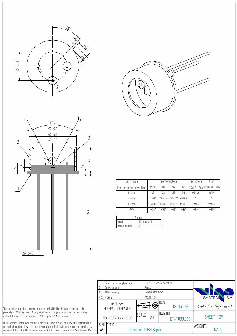
UNIT: mmGENERAL TOLERANCE:
X.X=±0.1 / X.XX=±0.05
18-Jul-16
TITLE:Detector TO39 3 pin
SIZE
A4
DWG NO:
DT-TO39.003SCALE:
WEIGHT:
SHEET 1 OF 1
Production Deparment
2:1
Date:No.
123
NameTO39 housing
Detector cap
Detector on sapphire pad
3u1 g
HgCdTe / GaAs / Sapphire
Material
Gold plated KovarBrass
The drawings and the information provided with the drawings are the soleproperty of VIGO System S.A. Any disclosure or reproduction, in part or whole,without the written permission of VIGO System S.A. is prohibited.
VIGO System's detectors contains miniature amounts of mercury and cadmium butas part of medical devices, monitoring and control instruments can be treated asan exempt from the UE Directive on the Restriction of Hazardous Substances (RoHS).
8.4O
5.5O
9.2O
4.713
.5
0.45O
3
2
1
R
0.4
FOV
5.08
O
45°
0.8
0.9
A
B
2
1
3
Lens shape Hyperhemisphere Hemisphere Flat
Detector optical area [mm²] 0.5x0.5 1x1 2x2 3x3 0.5x0.5 - 3x3 0.01x0.01 - 4x4
R [mm] 0.5 0.8 1.25 1.6 0.5-1.6 infity
A [mm] 1.5±0.2 2.4±0.2 3.75±0.2 4.8±0.2 0 0
B [mm] 1.9±0.2 1.9±0.2 1.9±0.2 1.9±0.2 1.9±0.2 1.9±0.2
FOV ~36° ~36° ~36° ~36° ~90° ~90°
Pin outSignal 1(+) and 2(-)Chassis Ground 3

UNIT: mmGENERAL TOLERANCE:
X.X=±0.1 / X.XX=±0.05
18-Jul-16
TITLE:Detector BNC
SIZE
A4
DWG NO:
DT-BNC.004SCALE:
WEIGHT:
SHEET 1 OF 1
Production Deparment
2:1
Date:No.
123
4
NameBNC connector - may vary from shown in drawing
Detector case
Detector cap
Detector on sapphire pad
25 u1 g
Material
Copper covered with Cr-Ni
HgCdTe / GaAs / Sapphire
Copper covered with Cr-Ni
The drawings and the information provided with the drawings are the soleproperty of VIGO System S.A. Any disclosure or reproduction, in part or whole,without the written permission of VIGO System S.A. is prohibited.
VIGO System's detectors contains miniature amounts of mercury and cadmium butas part of medical devices, monitoring and control instruments can be treated asan exempt from the UE Directive on the Restriction of Hazardous Substances (RoHS).
13O
27.7
±0.2
10.5
±1
40±1
AB
FOV
R
1
2
34
Lens shape Hyperhemisphere Hemisphere Flat
Detector optical area [mm²] 0.5x0.5 1x1 2x2 3x3 0.5x0.5 - 3x3 0.01x0.01 - 4x4
R [mm] 0.5 0.8 1.25 1.6 0.5-1.6 infity
A [mm] 4.6±0.3 5.5±0.3 6.85±0.3 7.9±0.3 3.1±0.3 1.6±0.3
B [mm] 3.1±0.15 3.1±0.15 3.1±0.15 3.1±0.15 3.1±0.15 1.6±0.15
FOV, C=Ø4 [mm] ~36° ~36° ~36° ~36° ~66° ~102°
FOV, C=Ø6 [mm] ~36° ~36° ~36° ~36° ~88° ~124°
C

UNIT: mmGENERAL TOLERANCE:
X.X=±0.1 / X.XX=±0.05
18-Jul-16
TITLE:Detector PEM
SIZE
A4
DWG NO:
DT-PEM.006SCALE:
WEIGHT:
SHEET 1 OF 12:1
Date:No.
123
4
5
6
NamePEM handle
Detector housing
Detector cap
Window
Detector on sapphire pad
SMA connector
25u1 g
Material
Black anodized Al
Black anodized SteelBlack anodized Al
ZnSe / other
HgCdTe / GaAs / Sapphire
Gold coated brass / PTFE
The drawings and the information provided with the drawings are the soleproperty of VIGO System S.A. Any disclosure or reproduction, in part or whole,without the written permission of VIGO System S.A. is prohibited.
VIGO System's detectors contains miniature amounts of mercury and cadmium butas part of medical devices, monitoring and control instruments can be treated asan exempt from the UE Directive on the Restriction of Hazardous Substances (RoHS).
Production Department
12.8
±0.2
24O
5O
22.8
±0.2
13O
6.4
21.9 ±0.3
10O
8
6.9
±0.2
1
2
35
6
4